JP4138155B2 - Method for manufacturing liquid discharge head - Google Patents
Method for manufacturing liquid discharge head Download PDFInfo
- Publication number
- JP4138155B2 JP4138155B2 JP15367999A JP15367999A JP4138155B2 JP 4138155 B2 JP4138155 B2 JP 4138155B2 JP 15367999 A JP15367999 A JP 15367999A JP 15367999 A JP15367999 A JP 15367999A JP 4138155 B2 JP4138155 B2 JP 4138155B2
- Authority
- JP
- Japan
- Prior art keywords
- piezoelectric
- head
- head substrate
- liquid discharge
- members
- Prior art date
- Legal status (The legal status is an assumption and is not a legal conclusion. Google has not performed a legal analysis and makes no representation as to the accuracy of the status listed.)
- Expired - Fee Related
Links
Images


Description
【0001】
【産業上の利用分野】
本発明は液体吐出ヘッドの製造方法に関し、特に積層型圧電素子を用いる液体吐出ヘッドの製造方法に関する。
【0002】
【従来の技術】
プリンタ、ファクシミリ、複写装置、プロッタ等の画像記録装置(画像形成装置を含む。)に用いるインクジェットヘッドは、インク滴を吐出するノズルと、このノズルが連通する液室(圧力室、加圧液室、吐出室、インク流路等とも称される。)と、この液室内のインクを加圧するエネルギーを発生するアクチュエータ手段(エネルギー発生手段)とを備えて、アクチュエータ手段を駆動することで吐出室内インクを加圧してノズルからインク滴を吐出させるものであり、記録の必要なときにのみインク滴を吐出するインク・オン・デマンド方式のものが主流である。
【0003】
そして、インク滴(記録液体)を吐出させるためのアクチュエータ手段の種類により、幾つかの方式に大別されるが、圧電素子などの積層型圧電素子を用いたピエゾ型インクジェットヘッドとしては、例えば特開平9−48132号公報に記載されているように、加圧液室を構成する壁面を圧電部材で形成し、シェアモード変形を利用してインク滴を吐出するようにしたものが知られている。
【0004】
このインクジェットヘッドにおいては、圧電部材を接着した後、所望のピッチに溝加工を施し、この溝に電極パターンを形成し、インクとの接触を防止するための絶縁膜を被覆するようにしている。そして、ノズル数を多くするために、少なくとも2枚以上の圧電部材を接着して大型の圧電部材を形成している。
【0005】
そして、この場合、圧電部材同士の接着層部が側壁の中に含まれると、接着層部を含む側壁のシェアモード変形が他の側壁のシェアモード変形より大幅に低下し、インク滴吐出性能が著しく低下するため、接着層部に溝が位置するように溝と側壁を形成し、接着層部が側壁に含まれないようにしたり、接着した圧電部材間の接着層部に対して複数個の側壁を斜めに交差させることにより、接着層部を複数の側壁中に分散させ、接着層部を含む側壁と接着層部を含まない側壁とのシェアモード変形量の誤差を少なくしている。
【0006】
また、ピエゾ型インクジェットヘッドとしては、特開平10−100401号公報に記載されているように、ヘッド基板上に複数の積層型圧電素子を配列して設け、この積層型圧電素子上に振動板、液室隔壁を形成する液室隔壁部材及びノズルを形成したノズルプレートを順次積層したものも知られている。このインクジェットヘッドは、圧電素子がインクに直接接触せず、圧電素子の発熱の影響も少なく、使用するインクに対する制限がないという利点があり、また圧電素子に駆動電圧を印加するための電極の引出の自由度も高い。
【0007】
【発明が解決しようとする課題】
上述したように積層型圧電素子を用いるインクジェットヘッドはシェアモード変形を利用するインクジェットヘッドに比べて多くの利点がある。しかしながら、積層型圧電素子は20〜50μm厚さの圧電層と数μm厚さの内部電極層とを交互に積層したものであり、一般的にはグリーンシート状の圧電層に電極層をスクリーン印刷で形成する工程を繰り返し、最後に何層にも積層されたシートを一体焼成して形成するため、焼成により圧電層と電極層との収縮差によって反りが発生し易く、反りの大きさはシートの面積と相関があることから、反りのない大型(長尺)の積層型圧電素子を得ることが困難である。
【0008】
そのため、記録密度の高密度化、記録速度の高速化などに対応するためにノズル数を多くした大型のヘッドやラインヘッドを構成することが困難であり、複数の積層型圧電部材を接着して、上記特開平9−48132号公報に記載されているように分割することが考えられる。しかしながら、同公報に記載されているように斜めに圧電部材を交差させると、積層型圧電素子の場合には電極の取り出しができなくなる。
【0009】
本発明は上記の課題に鑑みてなされたものであり、積層型圧電素子を用いた高速、高精度記録が可能な液体吐出ヘッドの製造方法を提供することを目的とする。
【0010】
【課題を解決するための手段】
上記の課題を解決するため、本発明に係る液体吐出ヘッドの製造方法は、ヘッド基板上に少なくとも2枚の積層型圧電部材を同一直線上に間隔を空けて並べて接合し、積層型圧電部材同士の対向する端面部分を含めて積層型圧電部材にスリット加工を施して、複数の積層型圧電素子を分割形成する構成とした。
【0011】
本発明に係る液体吐出ヘッドの製造方法は、ヘッド基板上に少なくとも2枚の積層型圧電部材を同一直線上に並べて接合し、この積層型圧電部材同士の対向する端面部分を加工開始位置としてスリット加工を施して、複数の積層型圧電素子に分割する構成とした。
【0014】
ここで、積層型圧電部材同士の対向する端面の間隔はスリット加工を施す切削手段の幅を越えないものとすることが好ましい。また、積層型圧電部材同士は予め仮留めした状態でヘッド基板に接合することが好ましい。
本発明に係る画像形成装置は、本発明に係るいずれかの液体吐出ヘッドを搭載したものである。
【0015】
【発明の実施の形態】
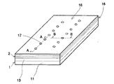
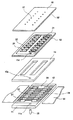
以下、本発明の実施の形態について添付図面を参照して説明する。図1は本発明の第1実施形態に係る液体吐出ヘッドとしてのインクジェットヘッドの一例を示す外観斜視図、図2は図1のA−A線に沿う要部拡大断面図、図3は図1のB−B線に沿う要部拡大断面図、図4は同インクジェットヘッドの分解斜視図である。
【0016】
このインクジェットヘッドは、アクチュエータユニット1と、このアクチュエータユニット1上に接合した液室ユニット2とからなる。
アクチュエータユニット1は、絶縁材からなるヘッド基板11上に、複数の積層型圧電素子12を複数列、列状に配置して接合し、これら各圧電素子12の周囲を取り囲む樹脂、セラミック等からなるフレーム部材(液室支持体)13を接着剤によって接合している。
【0017】
液室ユニット2は、振動板15上に加圧液室、共通インク流路等を形成する感光性樹脂フィルム(ドライフィルムレジスト)或いはSUSなどの金属プレートからなる液室隔壁部材16をドライフィルムレジストの熱圧着、或いは接着剤で接着し、この液室隔壁部材16上に複数のノズル17を形成したノズルプレート18を接着してなる。
【0018】
これらの振動板15、液室隔壁部材16及びノズルプレート17によって各圧電素子12に振動板15を介して対向する独立した複数の加圧液室21、各加圧液室21の両側に配置した共通インク流路22及び共通インク流路22から加圧液室21にインクを供給するインク供給路となる流体抵抗部23を形成している。
【0019】
ここで、ヘッド基板11は、厚さ0.5〜2mm程度で、しかも圧電素子に似た材質のものからなり、圧電素子と共に例えばダイヤモンド砥石による切削が可能なものであること、例えばチタン酸バリウム、アルミナ、ジルコンなどが好ましい。
【0020】
このヘッド基板11の圧電素子12の列設方向(ノズル列方向)と平行な両端部には、各列の個々の圧電素子12の対向しない端面側を接続するスリット溝26で分割された各圧電素子12に選択信号を与えるための個別電極27を形成し、また、各列間には各圧電素子12に駆動波形を与えるための共通電極28を形成している。さらに、インク供給パイプ29を接続するインク供給孔11aを設けている。
【0021】
また、圧電素子12は、10層以上の積層型圧電素子であり、厚さ20〜50μm/1層のPZT(=Pb(Zr・Ti)O3)30と、厚さ数μm/1層の銀・パラジューム(AgPd)からなる内部電極31とを交互に積層したものである。なお、圧電素子として用いる材料は上記に限られるものでなく、一般に圧電素子材料として用いられるBaTiO3、PbTiO3、(NaK)NbO3等の強誘電体などを用いることもできる。
【0022】
これら複数の圧電素子12は、後述するように、ヘッド基板11上に、同一直線上に並べて接合された2列、2枚の積層型圧電部材をスリット加工によるスリット溝26で分割して形成し、かつ、積層型圧電部材同士の対向する端面を含んでいないものである。
【0023】
そして、各列の圧電素子12の多数の内部電極31を1層おきに交互に両端面に取り出して、両端面に形成した例えばAgPdからなる端面電極32、33に接続し、各列の各圧電素子12の対向しない端面側の端面電極32をヘッド基板11上の個別電極27にヤング率200kgf/mm2以上の導電性ペーストなどの導電性材料35を介して接続し、各列の各圧電素子12の対向する端面側の端面電極33をヘッド基板11上の共通電極28に同じく導電性材料35を介して接続している。これらの個別電極27及び共通電極28はFPC36を介して図示しない駆動ICに接続される。
【0024】
さらに、フレーム部材13の圧電素子12の各列間に対応する部分の下面には、導電性ペースト(導電性接合剤)を全面に塗布して、スリット溝26で個々の圧電素子12(各チャンネル)毎に分割された共通電極28を相互に接続して一体の共通電極としている。なお、このフレーム部材13にもインク供給孔13aを形成している。
【0025】
次に、液室ユニット2の振動板15は、図3に示すように加圧液室21側は平坦面とし、圧電素子12側はそれぞれ厚みの異なるダイアフラム部15a、島状凸部15b、厚肉の接合領域15cを有している。この振動板15はNi(ニッケル)等の金属プレート、或いはSUS材と樹脂フィルムの積層体などから形成することができる。なお、振動板15にもインク供給孔15dを形成している。
【0026】
液室隔壁部材16は、振動板15上面とノズルプレート18との間に位置して加圧液室21等のインク流路を形成するものであり、その製造工程から下側隔壁部材41及び上側隔壁部材42で構成している。
【0027】
そして、この液室ユニット2は、その振動板15の島状凸部15bを接着剤20によって圧電素子12の上面に接合し、振動板15の厚肉部15cをフレーム部材13上面に接着剤20で接合することにより、アクチュエータユニット1に高い剛性で接合している。
【0028】
このインクジェットヘッドにおいては、記録信号に応じて選択的に圧電素子12に20〜50Vの駆動パルス電圧を印加することによって、パルス電圧が印加された圧電素子12が積層方向に変位して振動板15の対応するダイアフラム部15aを加圧液室21側に変形させ、加圧液室21の容積(体積)変化によって加圧液室21内のインクを加圧することで、インクがノズルプレート18のノズル17から液滴となって吐出され、記録を行うことができる。
【0029】
そして、インク滴の吐出に伴って加圧液室21内のインク圧力が低下し、このときのインク流れの慣性によって加圧液室21内には若干の負圧が発生する。この状態の下において、圧電素子12への駆動電圧の印加をオフ状態にすることによって、振動板15のダイアフラム部15aが元の位置に戻って加圧液室21が元の形状になるため、さらに負圧が発生する。このとき、図示しないインクタンクに通じるインク供給パイプ29から入ったインクは、共通インク流路22を通って流体抵抗部23から加圧液室21内に充填される。そして、ノズル17のインクメニスカス面の振動が減衰して安定した後、次のインク滴吐出のために圧電素子12にパルス電圧を印加する。
【0030】
この場合、振動板15の変形部をダイアフラム部15aとすることによって、圧電素子12の変位を効率的に加圧液室21に伝達することができると共に、当該加圧液室21以外の部分への振動の伝搬が減少してクロストークが低減する。また、インク滴吐出時に、加圧液室21から共通インク流路22に通じる流路方向にインクの流れが発生するが、この流路はその断面積を他より小さく形成した流体抵抗部23としているので、加圧液室21から共通インク流路22への逆流が極めて少なくなり、インク滴吐出効率の低下が防止される。
【0031】
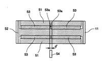
そこで、このインクジェットヘッドにおける圧電素子12の形成工程について図5乃至図8をも参照して説明する。なお、図5は積層型圧電部材を接着する前のヘッド基板を示す斜視説明図、図6は積層型圧電部材を接着したヘッド基板を示す斜視説明図、図7は図6の正面説明図、図8は図7の平面説明図である。
【0032】
ヘッド基板11には、図5に示すように、予めインク供給孔11aを形成し、個別電極パターン51と共通電極パターン52とをスクリーン印刷等で形成している。そして、図6乃至図8に示すように、このヘッド基板11上に、2つの積層型圧電部材53を同一直線上に間隔dを空けて並べて接着接合し、これを2列並列に配置する。このとき、図8に示すように、同一直線状に間隔dを空けて並べて接合された積層型圧電部材53を複数列有し、複数列を同時にスリット加工可能とする位置に間隔dを設けている。
【0033】
したがって、分割形成された積層型圧電素子12の各列の間隔も一度のスリット加工でスリット溝を形成できる間隔となる。これにより、スリット加工の作業効率が向上する。
【0034】
なお、この積層型圧電部材53は分割後に積層型圧電素子12となるものであって構造的には積層型圧電素子12と同じであり、またノズル列方向と同方向の両端面には分割後に端面電極32,33となる端面電極部材を形成し、導電性材料35で個別電極パターン51及び共通電極パターン52と電気的に接続する。
【0035】
そして、ダイシングソーやワイヤーソーなどのスリット加工を施す切削装置(スリット加工装置)を用いて、ダイヤモンド砥石などのブレードである切削部材54によって、積層型圧電部材53,53の長手方向と直交する方向に所定のピッチでスリット加工を施して、各列の積層型圧電部材53をスリット溝26によって分割して、複数の圧電素子12を形成する。なお、スリット溝26はヘッド基板11に達するまで形成することで、完全に圧電素子12を独立させ、クロストークを防止する。
【0036】
このとき、図7に示すようにブレード等の切削部材(切削手段)54によるスリット加工の開始位置は、2つの積層型圧電部材53、53の対向する端面(短手側端面)部分としている。
【0037】
また、2つの積層型圧電部材53、53の対向する端面(短手側端面)53a、53aの間隔dは切削手段であるブレード54の幅d’よりも狭くしている。
【0038】
これにより、2つの圧電部材53、53の対向する端面からスリット加工を開始することで、各圧電部材53,53間の間隔dが切削部材54の幅より狭いので、スリット加工により各圧電部材53の端面が除去され、分割形成された複数の積層型圧電素子12は圧電部材53の端面を含まないものとなり、等ピッチで長尺なヘッドを構成することができ、高速、高精度記録が可能になる。
【0039】
すなわち、ヘッド基板11上の圧電部材53の対向しない端面側からスリット加工を開始すると、複数の圧電部材53の接着時のずれ等によって、圧電部材53の対向する端面が積層型圧電素子12に含まれることがある。
【0040】
このように出来上がった積層型圧電素子12に端面が含まれると、圧電部材53、53の対向する端面53a、53aを接着した状態でヘッド基板11に接着した場合には、接着部分で積層型圧電素子12の駆動変位量が著しく低下し、安定したインク滴吐出が行えないと共に、インク滴吐出特性にチャンネル間のバラツキが生じることになる。
【0041】
また、圧電部材53、53の対向する端面53a、53aを接着しないでヘッド基板11上に接着した場合でも、対向する53a、53a端面を含む積層型圧電素子12はノズル列方向幅が他の積層型圧電素子12と異なることになり、インク滴吐出特性のバラツキが生じる。上述のように圧電部材53、53の対向する端面53a、53aを除去することで、これらの問題を回避することができる。
【0042】
また、2つの圧電部材53、53の対向する端面(短手側端面)53a、53aの間隔dをスリット加工を施すための切削手段54の幅d’よりも狭くして、その端面53a、53側からスリット加工を開始することで、一度のスリット加工で圧電部材53、53の端面53a、53を除去することができ、且つ、複数の積層型圧電素子12を等ピッチで形成できる。
【0043】
すなわち、2つの圧電部材53、53の対向する端面(短手側端面)53a、53aの間隔dがスリット加工を施すための切削手段54の幅d’よりも広くなると、2度の切削加工で圧電部材53の端面53a、53aを除去しなければならなくなる。この場合、複数の圧電素子12のピッチが不等間隔になると液室ユニット2と高精度に接合することができなくなり、インク滴吐出特性にバラツキが生じることになる。そのため、すべてのスリットで2度の切削加工を行わなければ分割された複数の圧電素子12間のピッチが等間隔でなくなってしまい、加工工数が極めて増加することになる。
【0044】
そこで、2つの圧電部材53、53の対向する端面(短手側端面)の間隔dを切削手段54の幅d’よりも狭くするのである。例えば、150dpiのヘッドの場合で、スリット溝26の幅を70μmとしたとき、2つの圧電部材53,53の対向する端面の間隔dは70μm以下、好ましくは50μm以下にする。同様に、例えば200dpiのヘッドの場合で、スリット溝26の幅を50μmとしたとき、2つの圧電部材53,53の対向する端面の間隔dは50μm以下、好ましくは30μm以下にする。
【0045】
すなわち、2つの圧電部材の対向する端面(短手側端面)の間隔dはスリット溝の幅(圧電素子12、12間の並置間隔)の0.5〜0.7倍程度にすることが、2つの圧電部材の接合作業を容易にし、また、スリット加工開始位置のマージンを持たせることができて、作業効率が向上する。
【0046】
また、2つの積層型圧電部材53、53の同一直線上での整列度は100μm以内にすることが好ましい。これにより、異なる積層型圧電部材53,53から形成された複数の積層型圧電素子12の整列度も100μm以内に収めることができる。
【0047】
すなわち、2つの積層型圧電部材53、53の整列度がずれた場合、振動板15のダイアフラム部15aと圧電素子12との接合位置ずれが生じて、振動板15の変位量が大きく低下し、更には液漏れを生じる原因となる。
【0048】
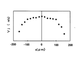
ここで、振動板15と圧電素子12の位置ずれ量とインク滴吐出速度Vjとの関係を図9に示している。適正なインク滴の吐出に最低7.0m/sの吐出速度Vjが必要であるとき、圧電素子12の長さLp=2000μm、振動板15のダイアフラム部15aの長さLd=1400μmである場合、同図に示すように、位置ずれ量が±100μmを越えると滴吐出速度Vjが大きく低下し、インク滴のバラツキが生じたり、吐出不良が生じる。したがって、振動板15と圧電素子12の位置ずれ量を100μm以内に収めるためには同一直線上に並ぶ2つの圧電部材53,53の整列度も100μm以内にする。
【0049】
ところで、2つの積層型圧電部材53,53を同一直線上に並べてヘッド基板11上に接着接合するには、例えば、圧電部材より若干大きな穴の空いた金属板などの冶具を用いて、定位置に圧電素子を落とし入れる方法、ヘッド基板11に突き当て冶具を配置して圧電部材の長尺側端面を突き当てる方法、画像処理を利用して位置決めする方法などを用いることができる。
【0050】
これらの方法を採用した場合でも複数の圧電部材を並べる煩雑さや設定位置ずれなどの問題が伴ない、特に2つの積層型圧電部材53、53の同一直線上での整列度を100μm以内に収めてヘッド基板11上に個々に接着する作業は手間である。
【0051】
そこで、2つの積層型圧電部材53、53を整列度が一定の範囲内に収まるように冶具などで位置出しして、圧電部材53,53の端面同士を予め接着剤などで仮留め(仮接着)しておき、仮留めした積層型圧電部材53、53をヘッド基板11上に接着することで、整列度を確保することができ、しかもヘッド基板への接着作業性を向上できる。なお、2つの積層型圧電部材53、53は仮留め接着剤のはみ出しがなく、ヘッド基板への接着面の平坦性を確保するように冶具で固定することが好ましい。
【0052】
以上のようにしてヘッド基板11上に複数の圧電素子12を分割形成した後、ヘッド基板11上にフレーム部材13を接着接合し、FPCケーブル36をヘッド基板11上の個別電極27及び共通電極28に熱と加圧で接合して、アクチュエータユニット1を完成する。なお、FPCケーブル36は圧電素子12を選択的に駆動できるパターンを有し、その接合部には予め半田メッキを施している。
【0053】
このアクチュエータユニット1とは別に液室ユニット2の加工・組み付けを行う。この液室ユニット2は、振動板15のフラットな面上に下側隔壁部材41を形成するための感光性樹脂である厚さ20〜50μm程度のドライフィルムレジストを熱及び加圧によってラミネートし、流路パターンに応じたマスクを用いて紫外線露光をして、露光部分を硬化させる。そして、未露光部分を除去できる溶剤を用いて、未露光部分を除去して現像し、図4に示すような下側隔壁部材41の液室パターンを形成し、水洗い、乾燥の後、再度紫外線と露光と熱によって本硬化する。また、ノズルプレート18にも同様にしてドライフィルムレジストを用いた上側隔壁部材42を形成する。
【0054】
次いで、振動板15とノズルプレート18に形成したドライフィルムレジストからなる下側隔壁部材41と上側隔壁部材42との対応する面同士を接合する。この接合は位置合わせ冶具を用いて行い、加圧及び前記本硬化のときより高い温度での加熱を行う。
【0055】
次に、上述のようにして完成したアクチユエータユニット1と液室ユニット2とを組み付ける。すなわち、先ず、アクチユエータユニット1の圧電素子12及びフレーム部材13の上面にスクリーン印刷機を用いてエポキシ系接着剤等の接着剤を塗布し、位置合わせ可能な接合治具にアクチユエータユニット1を固定し、液室ユニット2の振動板15側(接合面)を下方にして、位置合わせしながら両ユニット1、2を接合する。この場合、数kg/cm2の加圧状態でエポキシ系接着剤が反応硬化する間放置する。なお、接着剤として、アクリル系の二液非混合タイプのものやシアノアクリレート系のものなどを用いて瞬間的に接合するようにしてもよい。最後に、ヘッド基板11にインク供給パイプ29を挿入して接着剤を塗布硬化して固定する。
【0056】
このような製造工程を採用することにより、両ユニットの良品同士を選んで組み付けることが出できて、歩留まりが向上するとともに、加工組付け工程で粉塵が発生し易いアクチュエータユニット1と、粉塵の付着を避けたい液室ユニット2とを別々の工程で組み付けることができるので、完成したインクジェットヘッドの品質が向上する。
【0057】
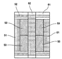
次に、本発明の第2実施形態について図10及び図11を参照して説明する。なお、図10はヘッド基板に積層型圧電部材を接着した状態の正面図、図11は同じく平面図である。
この実施形態では、ヘッド基板61には中央部に積層型圧電部材53端面が当接し、複数の積層型圧電部材53、53の列間距離を規定する段差部を形成する凸部62を形成している。なお、凸部62に代えて凹部を形成して段差部を形成することもできる。
【0058】
そこで、ヘッド基板61上に圧電部材53、53を接合するときに、圧電部材53、53の長手端面を凸部62で形成された段差部(凸部62の壁面)に当接させて冶具で押さえ込む。これによって、ヘッド基板61と圧電部材53、53を接合するときに、荷重を付加したときの位置ずれが低減する。なお、ヘッド基板61上の電極パターン51,52と導電性部材で電気的に接続することは前記実施形態と同様である。
【0061】
【発明の効果】
以上説明したように、本発明に係る液体吐出ヘッドの製造方法によれば、ヘッド基板上に少なくとも2枚の積層型圧電部材を同一直線上に間隔を空けて並べて接合し、積層型圧電部材同士の対向する端面部分を含めて積層型圧電部材にスリット加工を施して、複数の積層型圧電素子を分割形成する構成としたので、長尺のヘッドを実現でき、高速、高精度記録が可能になる。
【0062】
本発明に係る液体吐出ヘッドの製造方法によれば、ヘッド基板上に少なくとも2枚の積層型圧電部材を同一直線上に並べて接合し、この積層型圧電部材同士の対向する端面部分を加工開始位置としてスリット加工を施して、複数の積層型圧電素子に分割する構成としたので、長尺のヘッドを実現でき、高速、高精度記録が可能になる。
【0065】
ここで、積層型圧電部材同士の対向する端面の間隔はスリット加工を施す切削部材の幅を越えないものとすることで、分割後の積層型圧電素子に端面が含まれることなく、等ピッチの長尺なヘッドを得られる。また、積層型圧電部材同士は予め仮留めすることで、ヘッド基板への接着作業効率が向上する。
【図面の簡単な説明】
【図1】 本発明の第1実施形態に係るインクジェットヘッドの一例を示す外観斜視図
【図2】 図1のA−A線に沿う要部拡大断面図
【図3】 図1のB−B線に沿う要部拡大断面図
【図4】 同インクジェットヘッドの分解斜視図
【図5】 積層型圧電部材を接着する前のヘッド基板を示す斜視説明図
【図6】 積層型圧電部材を接着したヘッド基板を示す斜視説明図
【図7】 図6の正面説明図
【図8】 図7の平面説明図
【図9】 振動板と圧電素子のずれ量とインク滴吐出速度の関係の一例を説明する説明図
【図10】 本発明の第2実施形態におけるヘッド基板に積層型圧電部材を接着した状態の正面図
【図11】 同じく平面図
【符号の説明】
1…アクチュエータユニット、2…液室ユニット、11…ヘッド基板、12…積層型圧電素子、13…フレーム部材、15…振動板、16…液室隔壁部材、17…ノズル、18…ノズルプレート、53…積層型圧電部材。[0001]
[Industrial application fields]
The present invention is a liquid discharge headofManufacturing methodTo the lawIn particular, a liquid discharge head using a multilayer piezoelectric elementofManufacturing methodTo the lawRelated.
[0002]
[Prior art]
An ink jet head used in an image recording apparatus (including an image forming apparatus) such as a printer, a facsimile machine, a copying apparatus, or a plotter has a nozzle for ejecting ink droplets and a liquid chamber (pressure chamber, pressurized liquid chamber) communicating with the nozzle. And discharge chamber, ink flow path, etc.) and actuator means (energy generation means) for generating energy to pressurize the ink in the liquid chamber, and by driving the actuator means, the ink in the discharge chamber The ink-on-demand system is mainly used in which ink droplets are ejected from the nozzles by pressurizing the ink, and ink droplets are ejected only when recording is necessary.
[0003]
Depending on the type of actuator means for ejecting ink droplets (recording liquid), the ink jet head is roughly classified into several methods. For example, a piezo-type inkjet head using a laminated piezoelectric element such as a piezoelectric element is a special type. As described in Japanese Laid-Open Patent Application No. 9-48132, there is known a method in which a wall surface constituting a pressurized liquid chamber is formed of a piezoelectric member and ink droplets are ejected using shear mode deformation. .
[0004]
In this ink jet head, after bonding the piezoelectric member, a groove is formed at a desired pitch, an electrode pattern is formed in the groove, and an insulating film for preventing contact with ink is covered. In order to increase the number of nozzles, at least two piezoelectric members are bonded to form a large piezoelectric member.
[0005]
In this case, when the adhesive layer portion between the piezoelectric members is included in the side wall, the shear mode deformation of the side wall including the adhesive layer portion is significantly lower than the shear mode deformation of the other side wall, and the ink droplet ejection performance is improved. Since the groove is significantly lowered, the groove and the side wall are formed so that the groove is located in the adhesive layer part, and the adhesive layer part is not included in the side wall, or a plurality of adhesive layer parts between the bonded piezoelectric members are provided. By crossing the side walls diagonally, the adhesive layer portion is dispersed in a plurality of side walls, and the shear mode deformation amount error between the side wall including the adhesive layer portion and the side wall not including the adhesive layer portion is reduced.
[0006]
Further, as described in JP-A-10-100401, as a piezo-type inkjet head, a plurality of stacked piezoelectric elements are arranged on a head substrate, and a diaphragm, A liquid chamber partition member that forms a liquid chamber partition and a nozzle plate on which a nozzle is formed are sequentially stacked. This inkjet head has the advantage that the piezoelectric element is not in direct contact with the ink, the influence of heat generation of the piezoelectric element is small, and there is no restriction on the ink to be used. In addition, the extraction of the electrode for applying a drive voltage to the piezoelectric element The degree of freedom is high.
[0007]
[Problems to be solved by the invention]
As described above, an inkjet head using a laminated piezoelectric element has many advantages over an inkjet head using shear mode deformation. However, a laminated piezoelectric element is a laminate in which piezoelectric layers having a thickness of 20 to 50 μm and internal electrode layers having a thickness of several μm are alternately laminated. In general, an electrode layer is screen-printed on a green sheet-like piezoelectric layer. The process of forming is repeated, and finally the sheets laminated in multiple layers are integrally fired, so that the warpage is likely to occur due to the shrinkage difference between the piezoelectric layer and the electrode layer, and the size of the warp is the sheet Therefore, it is difficult to obtain a large (long) multilayer piezoelectric element without warping.
[0008]
Therefore, it is difficult to construct a large head or line head with a large number of nozzles in order to cope with higher recording density and higher recording speed. It is conceivable to divide as described in JP-A-9-48132. However, as described in the publication, when the piezoelectric members are crossed obliquely, in the case of the multilayer piezoelectric element, it becomes impossible to take out the electrodes.
[0009]
The present invention has been made in view of the above problems, and a liquid ejection head capable of high-speed and high-precision recording using a multilayer piezoelectric element.ofManufacturing methodThe lawThe purpose is to provide.
[0010]
[Means for Solving the Problems]
In order to solve the above problems, the liquid ejection head according to the present inventionManufacturing methodIsAt least two laminated piezoelectric members are aligned on the head substrate and spaced apart on the same straight line, and slits are applied to the laminated piezoelectric members including facing end surfaces of the laminated piezoelectric members. Split-type piezoelectric elementThe configuration.
[0011]
In the method of manufacturing a liquid ejection head according to the present invention, at least two laminated piezoelectric members are arranged on the same straight line on the head substrate and joined to each other, and the opposing end surface portions of the laminated piezoelectric members are slit as processing start positions. Processing was performed to divide into a plurality of stacked piezoelectric elements.
[0014]
Here, it is preferable that the interval between the opposing end surfaces of the laminated piezoelectric members does not exceed the width of the cutting means for performing the slit processing. Moreover, it is preferable that the laminated piezoelectric members are bonded to the head substrate in a state where they are temporarily secured.
An image forming apparatus according to the present invention is equipped with any of the liquid ejection heads according to the present invention.
[0015]
DETAILED DESCRIPTION OF THE INVENTION
Hereinafter, embodiments of the present invention will be described with reference to the accompanying drawings. FIG. 1 relates to a first embodiment of the present invention.As a liquid discharge head2 is an external perspective view showing an example of an inkjet head, FIG. 2 is an enlarged cross-sectional view of a main part taken along line AA in FIG. 1, FIG. 3 is an enlarged cross-sectional view of a main part taken along line BB in FIG. It is a disassembled perspective view of an inkjet head.
[0016]
The ink jet head includes an
The
[0017]
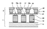
The liquid chamber unit 2 includes a liquid
[0018]
The
[0019]
Here, the
[0020]
Each of the piezoelectric elements divided by
[0021]
The
[0022]
As will be described later, the plurality of
[0023]
A large number of
[0024]
Further, a conductive paste (conductive bonding agent) is applied to the entire lower surface of the portion corresponding to the space between the
[0025]
Next, as shown in FIG. 3, the
[0026]
The liquid
[0027]
In the liquid chamber unit 2, the island-shaped
[0028]
In this ink jet head, by selectively applying a drive pulse voltage of 20 to 50 V to the
[0029]
And inkdropAs the ink is discharged, the ink pressure in the pressurized
[0030]
In this case, by making the deformed portion of the
[0031]
Therefore, the formation process of the
[0032]
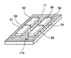
As shown in FIG. 5, the
[0033]
Therefore, the interval between the rows of the laminated
[0034]
The laminated
[0035]
Then, using a cutting device (slit processing device) that performs slit processing such as a dicing saw or a wire saw, a cutting
[0036]
At this time, as shown in FIG. 7, the slit machining start position by a cutting member (cutting means) 54 such as a blade is the end face (short-side end face) portion of the two laminated
[0037]
Further, the distance d between the opposing end faces (short-side end faces) 53a, 53a of the two laminated
[0038]
Accordingly, by starting slit processing from the opposing end surfaces of the two
[0039]
That is, when slit processing is started from the end surface side of the
[0040]
When the end face is included in the laminated
[0041]
Further, even when the
[0042]
Further, the distance d between the opposing end faces (short-side end faces) 53a, 53a of the two
[0043]
That is, when the distance d between the opposing end surfaces (short-side end surfaces) 53a, 53a of the two
[0044]
Therefore, the distance d between the opposing end surfaces (short-side end surfaces) of the two
[0045]
That is, the distance d between the opposing end faces (short-side end faces) of the two piezoelectric members should be about 0.5 to 0.7 times the width of the slit groove (the juxtaposition interval between the
[0046]
In addition, it is preferable that the degree of alignment of the two laminated
[0047]
That is, when the alignment degree of the two stacked
[0048]
Here, FIG. 9 shows the relationship between the positional deviation amount between the
[0049]
By the way, in order to arrange the two laminated
[0050]
Even when these methods are adopted, there are problems such as troublesome arrangement of a plurality of piezoelectric members and misalignment of set positions. Particularly, the alignment degree of the two laminated
[0051]
Therefore, the two stacked
[0052]
After a plurality of
[0053]
The liquid chamber unit 2 is processed and assembled separately from the
[0054]
Next, the corresponding surfaces of the
[0055]
Next, the
[0056]
By adopting such a manufacturing process, it is possible to select and assemble non-defective products of both units, improve the yield, and the
[0057]
Next, a second embodiment of the present invention will be described with reference to FIGS. FIG. 10 is a front view showing a state in which the laminated piezoelectric member is bonded to the head substrate, and FIG. 11 is a plan view of the same.
In this embodiment, the
[0058]
Therefore, when joining the
[0061]
【The invention's effect】
As described above, the liquid discharge head according to the present inventionProduction methodAccording toAt least two laminated piezoelectric members are aligned on the head substrate and spaced apart on the same straight line, and slits are applied to the laminated piezoelectric members including facing end surfaces of the laminated piezoelectric members. Therefore, a long head can be realized, and high-speed and high-precision recording is possible.
[0062]
According to the method for manufacturing a liquid ejection head according to the present invention, at least two stacked piezoelectric members are aligned on the head substrate and joined to each other, and the opposing end surface portions of the stacked piezoelectric members are processed at a processing start position. Since the slit processing is performed to divide into a plurality of laminated piezoelectric elements, a long head can be realized, and high-speed and high-precision recording is possible.
[0065]
Here, the interval between the opposing end faces of the multilayer piezoelectric members does not exceed the width of the cutting member to be slit, so that the end face is not included in the divided multilayer piezoelectric element, and the pitch is equal. A long head can be obtained. Further, by temporarily fastening the laminated piezoelectric members together, the efficiency of bonding work to the head substrate is improved.
[Brief description of the drawings]
FIG. 1 is an external perspective view showing an example of an inkjet head according to a first embodiment of the invention.
FIG. 2 is an enlarged cross-sectional view of a main part taken along line AA in FIG.
3 is an enlarged cross-sectional view of a main part taken along line BB in FIG.
FIG. 4 is an exploded perspective view of the same inkjet head.
FIG. 5 is a perspective explanatory view showing the head substrate before bonding the multilayer piezoelectric member.
FIG. 6 is a perspective explanatory view showing a head substrate to which a laminated piezoelectric member is bonded.
7 is an explanatory front view of FIG. 6. FIG.
FIG. 8 is an explanatory plan view of FIG.
FIG. 9 is an explanatory diagram illustrating an example of the relationship between the amount of displacement between the diaphragm and the piezoelectric element and the ink droplet ejection speed.
FIG. 10 is a front view showing a state in which a laminated piezoelectric member is bonded to a head substrate according to a second embodiment of the invention.
FIG. 11 is also a plan view
[Explanation of symbols]
DESCRIPTION OF
Claims (4)
Priority Applications (1)
| Application Number | Priority Date | Filing Date | Title |
|---|---|---|---|
| JP15367999A JP4138155B2 (en) | 1999-06-01 | 1999-06-01 | Method for manufacturing liquid discharge head |
Applications Claiming Priority (1)
| Application Number | Priority Date | Filing Date | Title |
|---|---|---|---|
| JP15367999A JP4138155B2 (en) | 1999-06-01 | 1999-06-01 | Method for manufacturing liquid discharge head |
Publications (3)
| Publication Number | Publication Date |
|---|---|
| JP2000334950A JP2000334950A (en) | 2000-12-05 |
| JP2000334950A5 JP2000334950A5 (en) | 2006-03-02 |
| JP4138155B2 true JP4138155B2 (en) | 2008-08-20 |
Family
ID=15567802
Family Applications (1)
| Application Number | Title | Priority Date | Filing Date |
|---|---|---|---|
| JP15367999A Expired - Fee Related JP4138155B2 (en) | 1999-06-01 | 1999-06-01 | Method for manufacturing liquid discharge head |
Country Status (1)
| Country | Link |
|---|---|
| JP (1) | JP4138155B2 (en) |
Families Citing this family (6)
| Publication number | Priority date | Publication date | Assignee | Title |
|---|---|---|---|---|
| JP2003094649A (en) * | 2001-09-21 | 2003-04-03 | Ricoh Co Ltd | Droplet discharge head |
| JP2006175845A (en) * | 2004-11-29 | 2006-07-06 | Ricoh Co Ltd | Liquid discharge head, liquid discharge apparatus, and image forming apparatus |
| JP5233130B2 (en) * | 2006-04-14 | 2013-07-10 | 株式会社リコー | Piezoelectric actuator, liquid ejection head, liquid ejection apparatus, image forming apparatus |
| JP4944687B2 (en) * | 2007-06-28 | 2012-06-06 | 株式会社リコー | Piezoelectric actuator and manufacturing method thereof, liquid ejection head, and image forming apparatus |
| JP5195198B2 (en) * | 2008-09-12 | 2013-05-08 | 株式会社リコー | Droplet discharge device, method for manufacturing two-row integrated piezoelectric element, and method for manufacturing droplet discharge device |
| JP2020049710A (en) * | 2018-09-25 | 2020-04-02 | 株式会社リコー | Liquid discharge head and liquid discharge device |
-
1999
- 1999-06-01 JP JP15367999A patent/JP4138155B2/en not_active Expired - Fee Related
Also Published As
| Publication number | Publication date |
|---|---|
| JP2000334950A (en) | 2000-12-05 |
Similar Documents
| Publication | Publication Date | Title |
|---|---|---|
| US5818482A (en) | Ink jet printing head | |
| JP3849145B2 (en) | Method for manufacturing piezoelectric actuator | |
| US6361152B1 (en) | Ink jet head and method of fabrication thereof | |
| WO1999000252A1 (en) | Piezoelectric vibrator unit, method for manufacturing the same, and ink-jet recording head | |
| JP2850762B2 (en) | Inkjet head | |
| JP4138155B2 (en) | Method for manufacturing liquid discharge head | |
| EP1083048A1 (en) | Ink jet recording head and manufacturing method thereof | |
| JP3231523B2 (en) | On-demand type inkjet head | |
| JP3330757B2 (en) | Ink jet head and method of manufacturing the same | |
| JP2008044296A (en) | Liquid jetting head | |
| JP3311514B2 (en) | Ink jet head and method of manufacturing the same | |
| JP2001071490A (en) | Ink-jet recording device | |
| JP2003019805A (en) | Ink jet head and its manufacturing method | |
| JP3185434B2 (en) | Inkjet print head | |
| JP4277477B2 (en) | Liquid jet head | |
| JP3539653B2 (en) | Inkjet head | |
| JPH11245406A (en) | Ink-jet head | |
| JP3298755B2 (en) | Method of manufacturing inkjet head | |
| JP2001054946A (en) | Ink-jet head | |
| JP4853175B2 (en) | Liquid jet head | |
| JP3232632B2 (en) | Inkjet print head | |
| JP3173189B2 (en) | Inkjet head | |
| JP2007168097A (en) | Method of manufacturing inkjet head | |
| JPH0825627A (en) | Ink jet head and manufacture thereof | |
| JPH06238895A (en) | Ink jet head and manufacture thereof |
Legal Events
| Date | Code | Title | Description |
|---|---|---|---|
| A621 | Written request for application examination |
Free format text: JAPANESE INTERMEDIATE CODE: A621 Effective date: 20041228 |
|
| A521 | Request for written amendment filed |
Free format text: JAPANESE INTERMEDIATE CODE: A523 Effective date: 20060108 |
|
| A977 | Report on retrieval |
Free format text: JAPANESE INTERMEDIATE CODE: A971007 Effective date: 20070315 |
|
| A131 | Notification of reasons for refusal |
Free format text: JAPANESE INTERMEDIATE CODE: A131 Effective date: 20070320 |
|
| A521 | Request for written amendment filed |
Free format text: JAPANESE INTERMEDIATE CODE: A523 Effective date: 20070521 |
|
| A131 | Notification of reasons for refusal |
Free format text: JAPANESE INTERMEDIATE CODE: A131 Effective date: 20070814 |
|
| A521 | Request for written amendment filed |
Free format text: JAPANESE INTERMEDIATE CODE: A523 Effective date: 20071012 |
|
| A02 | Decision of refusal |
Free format text: JAPANESE INTERMEDIATE CODE: A02 Effective date: 20080304 |
|
| A521 | Request for written amendment filed |
Free format text: JAPANESE INTERMEDIATE CODE: A523 Effective date: 20080402 |
|
| A911 | Transfer to examiner for re-examination before appeal (zenchi) |
Free format text: JAPANESE INTERMEDIATE CODE: A911 Effective date: 20080509 |
|
| TRDD | Decision of grant or rejection written | ||
| A01 | Written decision to grant a patent or to grant a registration (utility model) |
Free format text: JAPANESE INTERMEDIATE CODE: A01 Effective date: 20080526 |
|
| A01 | Written decision to grant a patent or to grant a registration (utility model) |
Free format text: JAPANESE INTERMEDIATE CODE: A01 |
|
| A61 | First payment of annual fees (during grant procedure) |
Free format text: JAPANESE INTERMEDIATE CODE: A61 Effective date: 20080605 |
|
| R150 | Certificate of patent or registration of utility model |
Free format text: JAPANESE INTERMEDIATE CODE: R150 |
|
| FPAY | Renewal fee payment (event date is renewal date of database) |
Free format text: PAYMENT UNTIL: 20110613 Year of fee payment: 3 |
|
| FPAY | Renewal fee payment (event date is renewal date of database) |
Free format text: PAYMENT UNTIL: 20110613 Year of fee payment: 3 |
|
| FPAY | Renewal fee payment (event date is renewal date of database) |
Free format text: PAYMENT UNTIL: 20120613 Year of fee payment: 4 |
|
| FPAY | Renewal fee payment (event date is renewal date of database) |
Free format text: PAYMENT UNTIL: 20130613 Year of fee payment: 5 |
|
| LAPS | Cancellation because of no payment of annual fees |