JP4102277B2 - Semiconductor integrated circuit device - Google Patents
Semiconductor integrated circuit device Download PDFInfo
- Publication number
- JP4102277B2 JP4102277B2 JP2003321059A JP2003321059A JP4102277B2 JP 4102277 B2 JP4102277 B2 JP 4102277B2 JP 2003321059 A JP2003321059 A JP 2003321059A JP 2003321059 A JP2003321059 A JP 2003321059A JP 4102277 B2 JP4102277 B2 JP 4102277B2
- Authority
- JP
- Japan
- Prior art keywords
- circuit
- terminal
- power supply
- potential
- protection
- Prior art date
- Legal status (The legal status is an assumption and is not a legal conclusion. Google has not performed a legal analysis and makes no representation as to the accuracy of the status listed.)
- Expired - Fee Related
Links
Images


Description
この発明は半導体集積回路装置に係わり、特に静電気放電から内部回路を保護する保護回路を有した半導体集積回路装置に関する。 The present invention relates to a semiconductor integrated circuit device, and more particularly to a semiconductor integrated circuit device having a protection circuit for protecting an internal circuit from electrostatic discharge.
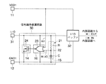
静電気放電(以下ESD)から内部回路を保護する保護回路、特に電源端子と接地端子との間に接続されたMOSFETを用いた電源端子保護回路の公知例を図13に示す。 FIG. 13 shows a known example of a protection circuit for protecting an internal circuit from electrostatic discharge (hereinafter referred to as ESD), particularly a power supply terminal protection circuit using a MOSFET connected between a power supply terminal and a ground terminal.
図13に示すように、電源端子保護回路は、RCディレイ回路101、インバータ回路102、ドライバNチャネル型MOSFET(以下NMOS)103とを含む。RCディレイ回路101は、電源端子VDDと接地端子GNDとの間に接続され、電源投入後、一定の時間が経過すると、その出力を“High”レベルとし、インバータ回路102を介して、ドライバNMOS103をオフさせる。即ち通電時には、ドライバNMOS103をオフさせ、電源端子VDDと接地端子GNDとの間の短絡を抑制し、半導体集積回路装置の誤動作を防止する。
As shown in FIG. 13, the power supply terminal protection circuit includes an
対して、電源端子VDDに対して短時間の高電圧印加、例えば、ESDが発生した際には、RCディレイ回路101は反応せず、その出力を“Low”レベルとし、インバータ回路102を介して、ドライバNMOS103をオンさせる。ドライバNMOS103がオンすることにより、例えば、電源端子VDDに印加された高電圧は放電され、半導体集積回路装置は破壊から保護される。
On the other hand, when a high voltage is applied to the power supply terminal VDD for a short time, for example, when ESD occurs, the
電源端子VDDの電源投入時の電位遷移は、ESD発生時の電位遷移に比較してゆっくりしている。RCディレイ回路101の時定数を、ESDのような短時間の電圧印加波形には反応しない値に設定しておけば、ドライバNMOS103が短時間の電圧印加時のみオンするようになり、保護素子として機能させることができる。この種の保護回路は、例えば、非特許文献1、2、3、4に記載されている。
The potential transition at power-on of the power supply terminal VDD is slower than the potential transition at the time of ESD occurrence. If the time constant of the
さらに、図14に示すように、RCディレイ回路101-1に加え、NAND回路102´の出力を、RCディレイ回路101-2、101-3を介して、自身の入力に帰還させ、通電時、ドライバNMOS103の誤動作をより確実に防止するようにした保護回路もある。この種の保護回路は、例えば、特許文献1に記載されている。
Furthermore, as shown in FIG. 14, in addition to the RC delay circuit 101-1, the output of the NAND circuit 102 'is fed back to its own input via the RC delay circuits 101-2 and 101-3. There is also a protection circuit that more reliably prevents the malfunction of the
図13及び図14に示す保護回路は、RCディレイ回路103を用いて、ドライバNMOS103をオフさせるようにしているので、例えば、電源端子のように、通電時において安定した電位を保つような端子には、適用することができる。しかしながら、高い周波数で“High”レベル、“Low”レベルを繰り返すような端子、例えば、入力/出力端子のような端子、いわば信号端子への適用は困難である。RCディレイ回路103は、高周波の電位印加に反応し難く、ドライバNMOS103を確実にオフさせることが難しいためである。特に、高速動作を要求するような半導体集積回路装置では、I/Oの信号伝播の遷移時間が、ESD印加時間に比べて短い場合もある。図13及び図14に示す保護回路では、このような信号が入力/出力される端子への適用が、事実上不可能になっている。
Since the protection circuit shown in FIGS. 13 and 14 uses the
また、図15に示すように、別の端子からの電位によって、保護素子の保護動作を制御するようにした保護回路もある。この種の保護回路は、例えば、非特許文献5に記載されている。 In addition, as shown in FIG. 15, there is a protection circuit in which the protection operation of the protection element is controlled by a potential from another terminal. This type of protection circuit is described in Non-Patent Document 5, for example.
図15に示す保護回路は、I/O端子保護回路であり、ドライバNMOS103のゲート電位を供給するための、ドライバNMOS103のゲートと入力/出力端子I/Oとの間に、ソースとドレインとを接続したPチャネル型MOSFET(以下PMOS)104を設けている。PMOS104のゲート電位は、入力/出力端子I/Oとは異なる端子、例えば、電源端子VDDから与えるようにしている。電源端子VDDは、通常動作の状態では、通電されて電源電位VDDとなっており、PMOS104のゲートには“High”レベルの電位が与えられている。これにより、通電時、PMOS104はオフし、ドライバNMOS103にゲート電位が供給されなくなり、ドライバNMOS103をオフさせることができる。従って、入/出力端子I/Oにも利用できるものとなっている。
The protection circuit shown in FIG. 15 is an I / O terminal protection circuit, and a source and a drain are connected between the gate of the
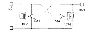
さらに、非特許文献5には、図16に示すように、電源端子VDD1と接地端子GNDとの間に接続されたドライバNMOS103-1の制御を、電源端子VDD2の電位によって制御し、電源端子VDD2と接地端子GNDとの間に接続されたドライバNMOS103-2の制御を、電源端子VDD1の電位によって制御する構成についても記載されている。
Further, in Non-Patent Document 5, as shown in FIG. 16, the control of the driver NMOS 103-1 connected between the power supply terminal VDD1 and the ground terminal GND is controlled by the potential of the power supply terminal VDD2, and the power supply terminal VDD2 A configuration is also described in which the control of the driver NMOS 103-2 connected between the power
図16に示す電源端子保護回路では、自身の電源端子以外の、電源端子の電位を利用して、PMOS104-1、又は104-2をオン/オフさせ、ドライバNMOS103-1、又は103-2をオン/オフさせる。このため、図13や図14に示したRCディレイ回路101を利用しなくても、自身の電源端子に印加された高電位を、放電することが可能になっている。しかしながら、図16に示す保護回路では、電源VDD2が通電されていない状態で、電源VDD1が通電されると、ドライバNMOS103-1がオンしてしまい、半導体集積回路装置が誤動作する。同じく、電源VDD1が通電されていない状態で、電源VDD2が通電されると、ドライバNMOS103-2がオンし、半導体集積回路装置が誤動作する。
In the power supply terminal protection circuit shown in FIG. 16, the PMOS 104-1 or 104-2 is turned on / off using the potential of the power supply terminal other than its own power supply terminal, and the driver NMOS 103-1 or 103-2 is turned on. Turn on / off. For this reason, it is possible to discharge the high potential applied to its own power supply terminal without using the
また、非特許文献6には、図17に示すように、電源端子VDD1と接地端子GNDとの間に接続されたドライバNMOS103-1の制御を、電源端子VDD2の電位を反転させるインバータ102-1によって制御し、電源端子VDD2と接地端子GNDとの間に接続されたドライバNMOS103-2の制御を、電源端子VDD1の電位を反転させるインバータ回路102-2によって制御する構成が記載されている。 In Non-Patent Document 6, as shown in FIG. 17, the control of the driver NMOS 103-1 connected between the power supply terminal VDD1 and the ground terminal GND is controlled by an inverter 102-1 that inverts the potential of the power supply terminal VDD2. The configuration in which the control of the driver NMOS 103-2 connected between the power supply terminal VDD2 and the ground terminal GND is controlled by the inverter circuit 102-2 that inverts the potential of the power supply terminal VDD1 is described.
図17に示す電源端子保護回路では、図16に示す電源端子保護回路と同様の動作を行うが、図16に示す電源端子保護回路と同様に、電源VDD2が通電されていない状態で、電源VDD1が通電されると、ドライバNMOS103-1がオンし、電源VDD1が通電されていない状態で、電源VDD2が通電されると、ドライバNMOS103-2がオンしてしまう。 The power supply terminal protection circuit shown in FIG. 17 performs the same operation as that of the power supply terminal protection circuit shown in FIG. 16. However, as with the power supply terminal protection circuit shown in FIG. Is turned on, and the driver NMOS 103-1 is turned on when the power supply VDD2 is turned on while the power supply VDD1 is not turned on.
現在の半導体集積回路装置には、多電源半導体集積回路装置が存在する。さらに、多電源半導体集積回路装置には、一部の回路を除いて、電源供給そのものをカットする、いわゆる部分的電源シャットダウン機能付の半導体集積回路装置も開発されるようになってきた。しかしながら、部分的電源シャットダウン機能付の半導体集積回路装置の電源端子に対して、図16や図17に示す保護回路を適用することはできない。例えば、電源VDD2がシャットダウンされた状態を仮定すると、ドライバNMOS103-1がオンし、電源端子VDD1と接地端子GNDとが短絡する。このため、半導体集積回路装置が誤動作する。
この発明は、部分的電源シャットダウン機能付の電源端子、及び信号端子のいずれにも適用することが可能な構成を持つ保護回路を備えた半導体集積回路装置を提供する。 The invention that provide a semiconductor integrated circuit device having a protection circuit with a power supply terminal dated partial power shutdown function, and any to which also can be applied the configuration of the signal terminals.
この発明の一態様に係る半導体集積回路装置は、第1電位が与えられる第1端子と、第2電位が与えられる第2端子と、第3電位が与えられる第3端子と、第4電位が与えられる第4端子と、前記第1端子と前記第2端子との間に接続された保護素子と、前記第3端子と前記第2端子との間に接続された第1電圧検知回路と、前記第1端子と前記第2端子との間に接続された第2電圧検知回路と、前記第4電位と前記第1電圧検知回路の出力とに基いて、前記保護素子の保護動作を許可及び禁止するとともに、前記第2電圧検知回路が前記第1電位と前記第2電位との電位差が所定の電位差を越えたことを検知したとき、前記第4電位及び前記第1電圧検知回路の出力に係わらずに、前記保護素子の保護動作を許可する保護素子動作制御回路とを具備する。 The semiconductor integrated circuit device according to one embodiment of this invention, a first terminal the first potential is applied, a second terminal a second potential is applied, and a third terminal of the third potential is applied, a fourth potential A fourth terminal, a protective element connected between the first terminal and the second terminal, a first voltage detection circuit connected between the third terminal and the second terminal, The protection operation of the protection element is permitted based on the second voltage detection circuit connected between the first terminal and the second terminal, the fourth potential, and the output of the first voltage detection circuit. And when the second voltage detection circuit detects that the potential difference between the first potential and the second potential exceeds a predetermined potential difference, the fourth potential and the output of the first voltage detection circuit Regardless of the protection element operation control circuit which permits the protection operation of the protection element It includes a.
この発明によれば、部分的電源シャットダウン機能付の電源端子、及び信号端子のいずれにも適用することが可能な構成を持つ保護回路を備えた半導体集積回路装置を提供できる。 According to the present invention, it is possible to provide a semiconductor integrated circuit device including a protection circuit having a configuration that can be applied to both a power supply terminal with a partial power supply shutdown function and a signal terminal.
以下、この発明の実施形態のいくつかを、図面を参照して説明する。この説明に際し、全図にわたり、共通する部分には共通する参照符号を付す。 Several embodiments of the present invention will be described below with reference to the drawings. In the description, common parts are denoted by common reference symbols throughout the drawings.
(第1実施形態)
図1はこの発明の第1実施形態に係る半導体集積回路装置の一回路例を示す回路図である。
(First embodiment)
FIG. 1 is a circuit diagram showing one circuit example of the semiconductor integrated circuit device according to the first embodiment of the present invention.
図1に示すように、第1実施形態に係る半導体集積回路装置は、電源端子保護回路10を有する。電源端子保護回路10は、第1端子11、第2端子12、及び第3端子13に接続されている。本実施形態において、第1端子11は第1電源電位VDD1が与えられる電源端子であり、第2端子12は低電位電源電位、例えば、接地電位GND1が与えられる接地端子であり、第3端子13は第2電源電位VDD2が与えられる電源端子である。
As shown in FIG. 1, the semiconductor integrated circuit device according to the first embodiment includes a power supply
保護素子14は、第1端子11と第2端子12との間に接続されている。
The
第1端子11と第2端子12との間には、さらに、電圧検知回路15が接続されている。
A
電圧検知回路15は、第1端子11と第2端子12との間の電圧を検知する。本実施形態において、電圧検知回路15は、いわば、通電安定検知回路であり、第1電源電位VDD1が投入されてから所定の時間が経過した後、保護素子14の保護動作を禁止する電位を、保護素子動作制御回路16に対して与える。このような回路の一例は、RCディレイ回路21である。本実施形態のRCディレイ回路21は、電流通路の一端に第1電源電位VDD1を受ける抵抗Rと、一方電極に接地電位GND1を受けるキャパシタCとを含む。そして、抵抗Rの電流通路の他端とキャパシタの他方電極との接続ノード22の電位を、保護素子動作制御回路16に与える。
The
保護素子動作制御回路16は、第2電源電位VDD2の電位と、電圧検知回路15の出力とに基いて、保護素子14の保護動作を許可及び禁止する制御を行う。保護素子動作制御回路16の一例は、例えば、第1電源電位VDD1と接地電位GND1との電位差を動作電源電圧とする論理回路である。本実施形態において、論理回路は、入力論理値として第2電源電位VDD2の電位と、電圧検知回路15の出力とを受ける。そして、第2電源電位VDD2及び電圧検知回路15の出力の少なくともいずれか一方の論理値が1状態、例えば、“High”レベルであるとき、保護素子14の保護動作を禁止する論理値を出力する。また、第2電源電位VDD2の電位及び電圧検知回路15の出力の双方の論理値が0状態、例えば、“Low”レベルであるとき、保護素子14の保護動作を許可する論理値を出力する。即ち論理回路は、第1電源電位VDD1及び第2電源電位VDD2のいずれか一方が通電されているとき、保護素子14の保護動作を禁止する論理値を出力し、双方が通電されていないとき、VDD1へのESD印加により、保護素子14の保護動作を許可する論理値を出力する。このような論理を出力する論理回路の一例は、NORゲート回路23である。
The protection element
保護素子14は、第1端子11と第2端子12との間に生じた高い電位差、例えば、ESD等から、第1端子11と第2端子12との間に接続された回路素子(図示せず)や集積回路(図示せず)を保護する。保護素子14は、このような保護動作をできる素子であれば良く、その一例は絶縁ゲート型FETである。本実施形態において、保護素子14は、ゲートを制御入力とし、ソース及びドレインの一方に第1電源電位VDD1を受け、ソース及びドレインの他方に接地電位GND1を受けるMOSFETである。MOSFETは、Nチャネル型MOSFET(NMOS)、Pチャネル型MOSFET(PMOS)のどちらも利用することができる。本実施形態では、NMOSを利用した例を示す。以下、保護動作を行うNMOSをドライバNMOS24と呼ぶ。本実施形態では、NORゲート回路22の出力は、ドライバNMOS24のゲートに直接に入力される。
The
次に、第1実施形態に係る半導体集積回路装置の動作を説明する。 Next, the operation of the semiconductor integrated circuit device according to the first embodiment will be described.
ドライバNMOS24は、NORゲート回路23の出力によって保護動作が許可されている状態で、第1端子11と第2端子12との間に、高い電位差が生じた時、例えば、ESDが発生した時にオンする。これによって、第1端子11と第2端子12との間に接続された回路素子(図示せず)や集積回路(図示せず)を保護する。
The
また、ドライバNMOS24は、NORゲート回路23の出力によって保護動作が禁止されている状態では、オフする。これによって、第1端子11と第2端子12との不慮の短絡を抑制し、集積回路の誤動作を抑制する。
The
以下、第1実施形態において、保護動作が許可される状態、及び禁止される状態を説明する。 Hereinafter, in the first embodiment, a state where the protection operation is permitted and a state where the protection operation is prohibited will be described.
(第1電源電位VDD1=通電、第2電源電位VDD2=通電)
第1電源電位VDD1、及び第2電源電位VDD2の双方が通電されている時、保護素子動作制御回路16、例えば、NORゲート回路23の第1入力IN1、及び第2入力IN2の双方の入力論理レベルが“High”となる。このため、NORゲート回路23は、その出力論理レベルを“Low”とする。これによって、保護素子14、例えば、ドライバNMOS24のゲート電位が“Low”となり、ドライバNMOS24はオフする。従って、保護素子14の保護動作が禁止され、半導体集積回路装置の誤動作が抑制される。
(First power supply potential VDD1 = energized, second power supply potential VDD2 = energized)
When both the first power supply potential VDD1 and the second power supply potential VDD2 are energized, the input logic of both the first input IN1 and the second input IN2 of the protection element
なお、本実施形態において、第1入力IN1には、RCディレイ回路21の出力が与えられる。故に、正確には、“第1電源電位VDD1=通電”の状態は、第1電源電位VDD1が通電されてから、RCディレイ回路21の時定数によって決まる、所定の遅延時間が経過した後、即ち第1電源電位VDD1の通電が安定した状態を指すことになる。
In the present embodiment, the output of the
(第1電源電位VDD1=通電、第2電源電位VDD2=未通電)
第1電源電位VDD1が通電され、第2電源電位VDD2が未通電である時、NORゲート回路23の第2入力IN2の入力論理レベルが“Low”となる。しかし、NORゲート回路23の第1入力IN1の入力論理レベルが“High”であるので、NORゲート回路23は、その出力論理レベルを、双方通電の状態と同様に、“Low”とする。この結果、ドライバNMOS24はオフする。従って、保護素子14の保護動作が禁止され、半導体集積回路装置の誤動作が抑制される。
(First power supply potential VDD1 = energized, second power supply potential VDD2 = not energized)
When the first power supply potential VDD1 is energized and the second power supply potential VDD2 is not energized, the input logic level of the second input IN2 of the NOR
(第1電源電位VDD1=未通電、第2電源電位VDD2=通電)
第1電源電位VDD1が未通電であり、第2電源電位VDD2が通電されている時、NORゲート回路23の第2入力IN2の入力論理レベルが“High”となるが、NORゲート回路23の電源VDD1が未通電あるため、その出力論理レベルは、双方通電の状態と同様に、“Low”と等価となる。
(First power supply potential VDD1 = not energized, second power supply potential VDD2 = energized)
When the first power supply potential VDD1 is not energized and the second power supply potential VDD2 is energized, the input logic level of the second input IN2 of the NOR
第1電源電位VDD1、及び第2電源電位VDD2の少なくとも一方が通電されてある状態の一例は、例えば、半導体集積回路装置が電子機器に組み込まれて、電源が投入れている状態である。 An example of a state in which at least one of the first power supply potential VDD1 and the second power supply potential VDD2 is energized is, for example, a state in which the semiconductor integrated circuit device is incorporated in an electronic device and the power is turned on.
本実施形態において、保護動作制御回路16は、第1電源電位VDD1、及び第2電源電位VDD2の少なくともどちらか一方が通電されていれば、保護素子14の保護動作は禁止される。つまり、本実施形態に係る半導体集積回路装置は、第1電源電位VDD1、及び第2電源電位VDD2のどちらか一方がシャットダウンされたとしても、保護素子14が動作せず、半導体集積回路装置の誤動作が抑制される。従って、本実施形態に係る半導体集積回路装置は、電源電位を部分的にシャットダウンする部分的シャットダウン機能付の半導体集積回路装置に適用することができる。
In the present embodiment, the protection
(第1電源電位VDD1=未通電、第2電源電位VDD2=未通電)
第1電源電位VDD1、及び第2電源電位VDD2の双方が未通電である時、NORゲート回路23の第1入力IN1、及び第2入力IN2の双方の入力論理レベルが“Low”となる。この状態で、例えば、第1端子11に対して高い電位が瞬間的に印加されたとする。ここで、瞬間的とは、例えば、RCディレイ回路21の遅延時間以下、もしくは未満の時間を指す。第1端子11に対して高い電位が瞬間的に印加された状態では、NORゲート回路23の第1入力IN1、及び第2入力IN2の双方の入力論理レベルが“Low”のままであるから、NORゲート回路23は、その出力論理レベルを、“High”とする。これによって、保護素子14、例えば、ドライバNMOS24のゲート電位が“High”となり、ドライバNMOS24はオンする。即ち保護素子14の保護動作が許可され、保護素子14が保護動作を行う。この結果、第1端子11と第2端子12との間に接続された回路素子(図示せず)や集積回路(図示せず)は、第1端子11に対して瞬間的に印加された高い電位、例えば、ESDから保護される。
(First power supply potential VDD1 = not energized, second power supply potential VDD2 = not energized)
When both the first power supply potential VDD1 and the second power supply potential VDD2 are not energized, the input logic levels of both the first input IN1 and the second input IN2 of the NOR
第1電源電位VDD1、及び第2電源電位VDD2の双方が未通電である状態の一例は、例えば、製造工場における組み立て前の状態である。組み立て前の半導体集積回路装置は、回路基板に実装されていない。このため、半導体集積回路装置の第1端子11、第2端子12、及び第3端子13のいずれもが、電気的接点に接続されていない状態にある。このような状態における半導体集積回路装置は、正電位か負電位かのいずれかに、不慮に帯電してしまうことがある。帯電した半導体集積回路装置に対して、半導体集積回路装置を搬送する搬送装置、例えば、ハンドラが接近したとする。ハンドラは、通常、接地されている。このため、帯電した半導体集積回路装置に対してハンドラが接近すると、ハンドラと半導体集積回路装置との間にESDが発生することがある。このようなESDが発生したときでも、本実施形態に係る半導体集積回路装置は、保護素子14の保護動作が許可されているので、半導体集積回路装置内の回路素子や集積回路は、静電破壊から保護することができる。
An example of a state in which both the first power supply potential VDD1 and the second power supply potential VDD2 are not energized is, for example, a state before assembly in a manufacturing factory. The semiconductor integrated circuit device before assembly is not mounted on the circuit board. For this reason, none of the
図2に、本実施形態における電源端子保護回路10の動作論理を示しておく。
FIG. 2 shows the operation logic of the power supply
第1実施形態に係る半導体集積回路装置によれば、自身の電源電位の通電状態と、自身の電源電位以外の、他の電源電位の通電状態とを参照して、自身の電源端子の保護動作を許可したり禁止したりすることが可能な電源端子保護回路10を有する。このため、自身の電源電位、及び他の電源電位の双方が未通電である時、保護素子14の保護動作を許可することができる。従って、例えば、半導体集積回路装置が組み立て前の状態において、不慮の高電位の印加、例えば、ESDが発生した時でも、内部の回路素子や集積回路を、静電破壊から保護することができる。
According to the semiconductor integrated circuit device of the first embodiment, the protection operation of its own power supply terminal with reference to the current supply state of its own power supply potential and the current supply state of other power supply potentials other than its own power supply potential The power supply
さらに、上記電源端子保護回路10は、自身の電源電位、及び他の電源電位の少なくともどちらか一方が通電されていれば、保護素子14の保護動作を禁止することができる。このため、上記電源端子保護回路10は、多電源半導体集積回路装置の電源端子、例えば、電源電位を部分的にシャットダウンする部分的電源シャットダウン機能付の電源端子にも適用することが可能である。
Further, the power supply
また、従来の保護回路に対して、本実施形態では保護素子動作制御回路16を付加する必要があるが、保護素子動作制御回路16は論理回路で構成することができる。しかし、論理回路を構成するMOSFET等の回路素子は、小さくて良いので面積の増加は、最小で済む。また、論理回路は、内部の集積回路に含まれる論理回路と同じ製造プロセスで形成することができるので、本実施形態に係る電源端子保護回路10は、製造プロセスを変更する必要もない。
Further, in this embodiment, the protection element
以上、第1実施形態によれば、部分的電源シャットダウン機能付の電源端子にも適用することが可能な構成を持つ保護回路を備えた半導体集積回路装置を得ることができる。 As described above, according to the first embodiment, it is possible to obtain a semiconductor integrated circuit device including a protection circuit having a configuration that can be applied to a power supply terminal with a partial power supply shutdown function.
(第2実施形態)
上記第1実施形態に示した構成を持つ保護回路は、電源端子ばかりでなく、信号端子の保護回路にも適用することが可能である。
(Second Embodiment)
The protection circuit having the configuration shown in the first embodiment can be applied not only to a power supply terminal but also to a signal terminal protection circuit.
以下、上記第1実施形態に示した構成を持つ保護回路を、信号端子、例えば、入力/出力端子に適用した例を、この発明の第2実施形態として説明する。 Hereinafter, an example in which the protection circuit having the configuration shown in the first embodiment is applied to a signal terminal, for example, an input / output terminal will be described as a second embodiment of the present invention.
図3はこの発明の第2実施形態に係る半導体集積回路装置の一回路例を示す回路図である。 FIG. 3 is a circuit diagram showing a circuit example of a semiconductor integrated circuit device according to the second embodiment of the present invention.
図3に示すように、第2実施形態に係る半導体集積回路装置が備える信号端子保護回路30は、第1実施形態に示した電源端子保護回路10と同様の構成を持つ。異なるところは、
(1) 保護素子14が、I/O端子31と第2端子12との間に接続されていること
(2) 電圧検知回路15が、I/O端子31と第2端子12との間に接続されていること
(3) 保護素子動作制御回路16が、第1電源電位VDDの電位と電圧検知回路15の出力とに基いて、保護素子14の保護動作を許可及び禁止する制御を行うこと、
である。
As shown in FIG. 3, the signal
(1) The
It is.
以下、第2実施形態において、保護動作が許可される状態、及び禁止される状態を説明する。 Hereinafter, in the second embodiment, a state where the protection operation is permitted and a state where the protection operation is prohibited will be described.
(第1電源電位VDD1=通電)
第1電源電位VDD1が通電されている時、保護素子動作制御回路16、例えば、NORゲート回路23の第1入力IN1の入力論理レベルが“High”となる。従って、NORゲート回路23は、第2入力INI/Oの入力論理レベルに係わらずに、その出力論理レベルを“Low”に固定する。この結果、ドライバNMOS24はオフし、保護素子14の保護動作が禁止される。従って、半導体集積回路装置の誤動作が抑制される。
(First power supply potential VDD1 = energized)
When the first power supply potential VDD1 is energized, the input logic level of the first input IN1 of the protection element
(第1電源電位VDD1=未通電)
第1電源電位VDD1が未通電の時、例えば、NORゲート回路23の第1入力IN1の入力論理レベルが“Low”となる。従って、NORゲート回路23は、第2入力INI/Oの入力論理レベルに従って、その出力論理レベルを“Low”、又は“High”とする。
(First power supply potential VDD1 = not energized)
When the first power supply potential VDD1 is not energized, for example, the input logic level of the first input IN1 of the NOR
本実施形態において、電圧検知回路15は、第1実施形態と同様のRCディレイ回路21である。このため、I/O端子31に対して瞬間的に高い電位が印加された時、即ち高い電位が、RCディレイ回路21の遅延時間以下、もしくは未満の時間内に印加された場合には、第2入力INI/Oの出力論理レベルは変化せず“Low”のままである。従って、NORゲート回路23は、その出力論理レベルを“High”とする。これによって、ドライバNMOS24のゲート電位が“High”となり、ドライバNMOS24がオンする。即ち保護素子14の保護動作が許可され、保護素子14が保護動作を行う。従って、I/O端子31に接続された回路素子や集積回路、例えば、I/Oバッファ32が、I/O端子31に対して瞬間的に印加された高い電位、例えば、ESDから保護される。
In the present embodiment, the
図4に、本実施形態における信号端子保護回路30の動作論理を示しておく。
FIG. 4 shows the operation logic of the signal
第2実施形態に係る半導体集積回路装置によれば、自身の電源電位の通電状態を参照して、自身のI/O端子の保護動作を許可したり禁止したりすることが可能な信号端子保護回路30を有する。このため、自身の電源電位が未通電である時、保護素子14の保護動作を許可することができる。従って、第1実施形態と同様に、例えば、半導体集積回路装置が組み立て前の状態において、不慮の高電位の印加、例えば、ESDが発生した時でも、内部の回路素子や集積回路、例えば、I/Oバッファ32を、静電破壊から保護することができる。
According to the semiconductor integrated circuit device according to the second embodiment, the signal terminal protection that allows or prohibits the protection operation of its own I / O terminal with reference to the energization state of its own power supply potential. A
さらに、上記信号端子保護回路30は、自身の電源電位が通電されていれば、保護素子14の保護動作を禁止することができる。このため、I/O端子31の電位が、信号論理振幅電圧で振れたとしても、ドライバNMOS24が動作することはない。
Furthermore, the signal
以上、第2実施形態によれば、電源電位が通電されている時、信号論理振幅電圧、例えば、“High”レベルと“Low”レベルとを繰り返すような端子、例えば、I/O端子のような信号端子にも適用することが可能な信号端子保護回路を得ることができる。 As described above, according to the second embodiment, when the power supply potential is energized, the signal logic amplitude voltage, for example, a terminal that repeats the “High” level and the “Low” level, for example, an I / O terminal, etc. It is possible to obtain a signal terminal protection circuit that can be applied to various signal terminals.
なお、多電源半導体集積回路装置においては、第1電源電位VDD1が未通電の時、I/O端子31の電位が、第1電源電位VDD1レベル、例えば、信号の論理レベル“High”となる場合もあり得る。
In the multi-power supply semiconductor integrated circuit device, when the first power supply potential VDD1 is not energized, the potential of the I /
しかし、この場合には、半導体集積回路装置内で、I/Oバッファ32を構成するPMOSの、I/O端子31に接続されるP+型ドレイン拡散層と、シャットダウンされた第1電源電位VDD1に接続されるN型ウェルとの間に形成されたダイオードが順方向にバイアスされて、ブレークダウンする。その上、電源がシャットダウンされたI/Oバッファ32に対しては“Low”レベルを供給する、という、回路設計上の制約が与えられるので、問題はない。
However, in this case, in the semiconductor integrated circuit device, the P + type drain diffusion layer connected to the I /
また、本実施形態では、信号端子保護回路30の適用例として、I/O端子31に適用した例を説明したが、入力信号や出力信号を取り扱うI/O端子に限らず、コマンド信号を取り扱うコマンド信号端子、クロック信号を取り扱うクロック信号端子等、さまざまな信号端子に適用することができる。
In the present embodiment, an example in which the signal
(第3実施形態)
第3実施形態は、第1、第2実施形態において説明した保護回路を、多電源半導体集積回路装置に適用した場合の具体的一回路例に関している。
(Third embodiment)
The third embodiment relates to a specific circuit example when the protection circuit described in the first and second embodiments is applied to a multi-power supply semiconductor integrated circuit device.
図5はこの発明の第3実施形態に係る半導体集積回路装置の一回路例を示す回路図である。 FIG. 5 is a circuit diagram showing a circuit example of a semiconductor integrated circuit device according to the third embodiment of the present invention.
図5に示すように、第3実施形態に係る半導体集積回路装置は、第1電源端子保護回路10-1、第2電源端子保護回路10-2、及び信号端子保護回路30を有する。本実施形態において、第1電源端子保護回路10-1は第1実施形態と同様のものであり、信号端子保護回路30は第2実施形態と同様のものであるので、その説明は省略する。
As shown in FIG. 5, the semiconductor integrated circuit device according to the third embodiment includes a first power supply terminal protection circuit 10-1, a second power supply terminal protection circuit 10-2, and a signal
第2電源端子保護回10-2は、第1実施形態に示した電源端子保護回路10と同様の構成を持つ。異なるところは、
(1) 保護素子14が、第3端子13と第4端子33との間に接続されていること、
(2) 電圧検知回路15が、第3端子13と第4端子33との間に接続されていること、
(3) 保護素子動作制御回路16が、第1電源電位VDDの電位と電圧検知回路15の出力とに基いて、保護素子14の保護動作を許可及び禁止する制御を行うこと、
である。ここで、第4端子33は、接地電位GND2が与えられる接地端子である。本実施形態では、接地電位が与えられる端子を、第2端子12と第4端子33とに分けているが、第4端子33は第2端子12であっても良い。
The second power supply terminal protection circuit 10-2 has the same configuration as the power supply
(1) the
(2) The
(3) the protection element
It is. Here, the
第2電源端子保護回路10-2の保護動作が許可される状態、及び禁止される状態は、第1実施形態に示した電源端子保護回路10と同様であり、第1電源電位VDD1、及び第2電源電位VDD2の少なくとも一方が通電されていれば、保護素子14の保護動作が禁止され、半導体集積回路装置の誤動作が抑制される。また、第1電源電位VDD1、及び第2電源電位VDD2の双方が未通電の時に、保護素子14の保護動作が許可され、半導体集積回路装置を、例えば、静電破壊から保護することができる。
The state where the protection operation of the second power supply terminal protection circuit 10-2 is permitted and the state where the protection operation is prohibited are the same as those of the power supply
第3実施形態によれば、多電源半導体集積回路装置、例えば、第1電源電位VDD1、第2電源電位VDD2のように、複数の電源が与えられる半導体集積回路装置において、第1電源(VDD1)端子保護回路10-1、及び第2電源(VDD2)端子保護回路の双方ともが、自身の電源電位、及び他の電源電位の少なくともどちらか一方が通電されていれば、保護素子14の保護動作を禁止することができる。従って、多電源半導体集積回路装置のそれぞれの電源端子に接続された回路素子や集積回路を、誤動作を抑制したまま、例えば、静電破壊から保護することができる。
According to the third embodiment, in a multi-power supply semiconductor integrated circuit device, for example, a semiconductor integrated circuit device to which a plurality of power supplies are provided such as a first power supply potential VDD1 and a second power supply potential VDD2, the first power supply (VDD1). If both the terminal protection circuit 10-1 and the second power supply (VDD2) terminal protection circuit are energized at least one of their own power supply potential and the other power supply potential, the protection operation of the
(第4実施形態)
第4実施形態は、保護素子14に、PMOSを用いた例である。
(Fourth embodiment)
The fourth embodiment is an example in which a PMOS is used for the
図6はこの発明の第4実施形態に係る半導体集積回路装置の一回路例を示す回路図である。 FIG. 6 is a circuit diagram showing a circuit example of a semiconductor integrated circuit device according to the fourth embodiment of the present invention.
図6に示すように、保護素子14には、NMOS24ばかりでななく、PMOS24´を用いることが可能である。この場合には、保護素子動作制御回路16の論理回路の出力論理を、反転させれば良い。本実施形態においては、論理回路として、NORゲート回路23の出力にインバータ回路を接続し、その論理論理を反転させたORゲート回路23´を用いている。
As shown in FIG. 6, not only the
第4実施形態によれば、第1〜第3実施形態と同様の効果を得ることが可能な、保護素子14としてPMOS24´を用いた保護回路を得ることができる。
According to the fourth embodiment, it is possible to obtain a protection circuit using the
(第5実施形態)
第1〜第4実施形態に示した電圧検知回路15は、例えば、電源の通電が行われて所定の遅延時間が経過すると、保護素子14の保護動作を禁止してしまうように構成されている。
(Fifth embodiment)
The
ESDには、組み立て前の任意の2端子間への電圧印加を扱う以外に、EMS(電磁妨害感受性)規格IEC16000−4−2の様に、セットとなって組み立てられて、通電されている状態でも、外部から静電気を印加して誤動作や破損の有無を調べ、その感受性の強靭さを試験する場合がある。 In addition to handling voltage application between any two terminals before assembly, the ESD is assembled and energized as in EMS (Electromagnetic Interference Susceptibility) standard IEC16000-4-2 However, there are cases in which the external device is examined for the presence of malfunctions and damage by applying static electricity to test its toughness.
この場合、例えば、RCディレイ回路21のような電圧検知回路15では、通電状態において、ドライバNMOS24の保護動作が禁止されてしまうために、静電気によって生じた電荷を、有効に放電させることができない。通電状態においても、有効な放電を行わせたい場合、あるいは行わせる必要がある半導体集積回路装置に対しては、検出回路を高閾値レベル検出型とすると良い。検出回路を高閾値レベル検出型とすることによって、通電されている状態でも、例えば、ESDによって生じた高い電位差に反応する保護回路を得ることができる。
In this case, for example, in the
図7はこの発明の第5実施形態に係る高閾値レベル検出型検知回路の第1例を示す回路図である。 FIG. 7 is a circuit diagram showing a first example of a high threshold level detection type detection circuit according to a fifth embodiment of the present invention.
図7に示すように、第1例に係る高閾値レベル検出型検知回路21´は、抵抗Rと、抵抗Rに直列に接続されたダイオード回路Dとを有する。本例のダイオード回路Dはダイオードを複数含み、これら複数のダイオードは互いに直列に接続されている。ダイオードDの直列接続数は、例えば、検知すべき電圧値によって適宜調節される。抵抗Rの電流通路の一端には、第1電位、例えば、高電位側電源電位VDDが与えられる。ダイオード回路Dのカソードには、第2電位、例えば、低電位側電源電位VSS(以下接地電位)が与えられる。抵抗Rの電流通路の他端は、ダイオード回路Dのアノードに接続され、この接続ノード22の電位が、保護素子動作制御回路16の入力、例えば、NORゲート回路23の入力の一つに与えられる。
As shown in FIG. 7, the high threshold level detection
検知回路21´は、抵抗RとダイオードDとを直列接続した回路であり、ノード22の電位は、{ダイオードの順方向電圧VF×ダイオードの直列接続数}で一定である。ノード22の一定の電位は、保護素子動作制御回路16の入力に与えられる。この状態で、高電位側電源電位VDDの電位が上昇すると、抵抗Rの電圧降下が大きくなり、保護素子動作制御回路16の入力の電位と電源電位VDDとの電位差が大きくなる。この電位差が所定の電位差を超えたときにESDを検知した、とすることで、保護素子14の保護動作を許可することができる。
The
第1例に係る検知回路21´によれば、電源電位VDDと接地電位VSSとの電位差が所定の電位差VDDに達している状態において、さらに、所定の電位差VDDを超える電位差が生じたことを検知することができる。そして、この検知結果を、保護素子動作制御回路16に与えることによって、たとえ通電状態であっても、保護素子14の保護動作を許可することが可能となる。
According to the
図8は高閾値レベル検出型検知回路の第2例を示す回路図である。 FIG. 8 is a circuit diagram showing a second example of the high threshold level detection type detection circuit.
図8に示すように、第2例に係る高閾値レベル検出型検知回路21´´は、抵抗Rと、抵抗Rに直列に接続されたダイオード回路Dと、抵抗Rとダイオード回路Dとの接続ノード22に入力を接続したインバータ回路34とを有する。ダイオード回路Dのアノードには、例えば、電源電位VDDが与えられる。抵抗Rの電流通路の一端には、例えば、接地電位VSSが与えられる。ダイオード回路Dのカソードは、抵抗Rの電流通路の他端に接続され、この接続ノード22の電位が、インバータ回路34の入力に与えられる。インバータ回路34の出力は、保護素子制御回路16の入力、例えば、NORゲート回路23の入力の一つに与えられる。
As shown in FIG. 8, the high threshold level detection
検知回路21´´は、電源電位VDDと接地電位VSSとの電位差が所定の電位差、即ちVDDに達している状態において、ノード22の電位を低い電位、即ち出力論理レベルを“Low”とする。論理値“Low”の電位が、インバータ回路34の入力に与えられ、この入力を受けてインバータ回路34は、その出力論理レベルを“High”とする。論理値“High”の出力が、例えば、NORゲート回路23の入力の一つに与えることによって、保護素子14の保護動作が禁止される。
In a state where the potential difference between the power supply potential VDD and the ground potential VSS reaches a predetermined potential difference, that is, VDD, the
また、電源電位VDDと接地電位VSSとの電位差が所定の電位差より高くなるにつれて、ノード22の電位は上昇する。ノード22の電位がインバータ回路34の回路閾値を超えると、インバータ回路34は、その出力論理レベルを“High”から“Low”とする。論理値“Low”の出力が、例えば、NORゲート回路23の入力の一つに与えることによって、保護素子14の保護動作が許可される。
Further, as the potential difference between the power supply potential VDD and the ground potential VSS becomes higher than a predetermined potential difference, the potential of the
第2例に係る検知回路21´´においても、電源電位VDDと接地電位VSSとの電位差が所定の電位差VDDに達している状態において、さらに、所定の電位差VDDを超える電位差が生じたことを検知することができ、第1例と同様に、たとえ通電状態であっても、保護素子14の保護動作を許可することが可能となる。検知回路21´´の回路閾値は、電源電圧を超え、保護素子14のホールド電圧未満であれば良い。
Also in the
なお、第2例に係る検知回路21´´において、インバータ回路34は省略することが可能である。即ちノード22の電位を、保護素子動作制御回路16に直接に入力し、接続ノード22の電位に応じて、保護素子動作制御回路16が、保護素子14の保護動作を禁止したり、許可したりすることも可能である。
In the
また、検知回路21´、21´´には、RCディレイ回路21に比較して、次のような利点がある。RCディレイ回路21は、時定数の調節/設定、即ち遅延時間の調節/設定のために、キャパシタCを有する。キャパシタCは、半導体チップ上で大きな面積を必要とする。対して、検知回路21´、21´´ではキャパシタCを必要としないので、電圧検知回路15のサイズを、より小さくすることが可能である。
In addition, the
(第6実施形態)
第6実施形態は、通電時においても動作可能な保護回路の、別の例である。
(Sixth embodiment)
The sixth embodiment is another example of a protection circuit operable even when energized.
図9はこの発明の第6実施形態に係る半導体集積回路装置の一回路例を示す回路図である。 FIG. 9 is a circuit diagram showing one circuit example of a semiconductor integrated circuit device according to the sixth embodiment of the present invention.
図9に示すように、第6実施形態に係る半導体集積回路装置は、信号端子保護回路30´を有する。信号端子保護回路30´は、保護素子14と、第1端子11と第2端子12との間に接続された第1電圧検知回路15-1と、I/O端子31と第2端子12との間に接続された第2電圧検知回路15-2と、第1保護素子動作制御回路16-1と、第1保護素子動作制御回路16-1の出力に接続された入力を有する第2保護素子動作制御回路16-2とを有する。
As shown in FIG. 9, the semiconductor integrated circuit device according to the sixth embodiment includes a signal
本実施形態において、保護素子14は、ドライバNMOS24であり、第1電圧検知回路15-1はRCディレイ回路21であり、第2電圧検知回路15-2は高閾値レベル検出型検知回路21´´である。また、第1保護素子動作制御回路16-1、及び第2保護素子動作制御回路16-2は、回路的に1つの保護素子動作制御回路を構成し、第2電源電位VDD2の電位、第1電圧検知回路15-1の出力、及び第2電圧検知回路15-2の出力に基いて、保護素子14の保護動作を許可したり禁止したりする制御を行う。
In the present embodiment, the
本実施形態において、第1保護素子動作制御回路16-1は、第1電源電位VDD1と接地電位GND1との電位差を動作電源電圧とする論理回路、例えば、NORゲート回路23である。NORゲート回路23は、入力論理値として第2電源電位VDD2の電位と、第1電圧検知回路15-1の出力とを受ける。その動作は、例えば、第1実施形態に示した電源端子保護回路10の、保護素子動作制御回路16の、NORゲート回路23と同様である。
In the present embodiment, the first protection element operation control circuit 16-1 is a logic circuit that uses the potential difference between the first power supply potential VDD1 and the ground potential GND1 as an operation power supply voltage, for example, a NOR
また、第2保護素子動作制御回路16-2は、I/O端子31の電位と接地電位GND1との電位差を動作電源電圧とする論理回路、例えば、ORゲート回路23´である。ORゲート回路23´は、入力論理値として第1保護素子動作制御回路16-1の出力と第2電圧検知回路15-2とを受ける。ORゲート回路23´は、第2電圧検知回路15-2の出力論理レベルが“Low”、例えば、I/O端子31の電位と接地電位GND1との電位差が所定の電位差以下である時、第1保護素子動作制御回路16-1の出力論理値に従って、保護素子14の保護動作を許可したり禁止したりする。
The second protection element operation control circuit 16-2 is a logic circuit that uses the potential difference between the potential of the I /
例えば、ORゲート回路23´は、第2電圧検知回路15-2の出力論理レベルが“Low”であり、かつ第1保護素子動作制御回路16-1の出力論理レベルが“Low”であるとき、その出力論理レベルを“Low”とし、保護素子14の保護動作を禁止する。反対に、第2電圧検知回路15-2の出力論理レベルが“Low”であり、かつ第1保護素子動作制御回路16-1の出力論理レベルが“High”であるとき、その出力論理レベルを“High”とし、保護素子14の保護動作を許可する。
For example, in the
また、第2電圧検知回路の15-2の出力論理レベルが“High”となったとき、即ち、I/O端子31の電位と接地電位GND2との電位差が所定の電位差を超えたとき(過電圧検知)、ORゲート回路23´は、第1保護素子動作制御回路16-1の出力論理レベルに係わらずに、その出力論理レベルを“High”とし、保護素子14の保護動作を許可する。
Further, when the output logic level of 15-2 of the second voltage detection circuit becomes “High”, that is, when the potential difference between the potential of the I /
図10に、本実施形態における信号端子保護回路10の動作論理を示しておく。
FIG. 10 shows the operation logic of the signal
第6実施形態に係る半導体集積回路装置によれば、通電時に、例えば、I/O端子に、所定の電位差を越える電位差が印加されたとき、保護素子14、例えば、ドライバNMOS24の保護動作を許可する。このため、通電時において、半導体集積回路装置を、過大な電圧から保護することができる。
According to the semiconductor integrated circuit device of the sixth embodiment, during energization, for example, when a potential difference exceeding a predetermined potential difference is applied to the I / O terminal, the protection operation of the
(第7実施形態)
第7実施形態は、第6実施形態の保護素子14に、PMOSを用いた例である。
(Seventh embodiment)
The seventh embodiment is an example in which a PMOS is used for the
図11はこの発明の第7実施形態に係る半導体集積回路装置の一回路例を示す回路図である。 FIG. 11 is a circuit diagram showing one circuit example of a semiconductor integrated circuit device according to the seventh embodiment of the present invention.
図11に示すように、保護素子14にPMOS24´を用いた場合には、第2保護素子動作制御回路16-2の論理回路の出力論理を、反転させれば良い。本実施形態においては、ORゲート回路23´に代えて、NORゲート回路23を用いている。
As shown in FIG. 11, when the PMOS 24 'is used as the
第7実施形態によれば、第6実施形態と同様の効果を得ることが可能な、PMOS24´を保護素子14に用いた保護回路を得ることができる。
According to the seventh embodiment, it is possible to obtain a protection circuit using the
(第8実施形態)
図12はこの発明の第8実施形態に係る半導体集積回路装置の一回路例を示す回路図である。
(Eighth embodiment)
FIG. 12 is a circuit diagram showing an example of a semiconductor integrated circuit device according to the eighth embodiment of the present invention.
強靭なESD耐量が必要な場合には、ドライバNMOS24のサイズを大きくすることが必要である。この場合には、NORゲート回路23の駆動能力とドライバNMOS24のゲート負荷容量との兼ね合いで、ドライバNMOS24がオンされるのに、必要以上の時間がかかってしまう可能性がある。
When a strong ESD tolerance is required, it is necessary to increase the size of the
このような場合には、図12に示すように、保護素子動作制御回路16の出力、例えば、NORゲート回路23の出力と、保護素子14の制御入力、例えば、ドライバNMOS24のゲートとの間にプリドライバ回路40を挿入し、ドライバNMOS24のゲートを、プリドライバ回路40を介して駆動するようにすれば良い。
In such a case, as shown in FIG. 12, between the output of the protection element
プリドライバ回路40は、例えば、複数のインバータ回路41を直列接続することによって構成される。そして、各インバータ回路41は、例えば、保護素子動作制御回路16の出力から保護素子14の制御入力に向かって、次第にサイズが大きくされ、次第に駆動能力が大きくされる。
The
第8実施形態によれば、プリドライバ回路41を設けるので、保護素子14の制御入力の負荷容量が大きな保護素子14を、例えば、サイズの小さい論理回路、いわば駆動能力の小さい論理回路でも駆動することが可能となる。
According to the eighth embodiment, since the
以上、第1〜第8実施形態によれば、多数の電源端子を有し、部分的電源シャットダウンを行うなどの複雑な電源システムを用いた多電源半導体集積回路装置においても、ESD時の確実な保護と通常時のシステム動作への透明性(動作に影響を与えないこと)を確保した保護回路、さらに、I/O端子等の信号端子にも適用可能な保護回路を提供することができる。 As described above, according to the first to eighth embodiments, even in a multi-power supply semiconductor integrated circuit device using a complicated power supply system having a large number of power supply terminals and performing a partial power supply shutdown, it is possible to reliably perform ESD. It is possible to provide a protection circuit that ensures protection and transparency to normal system operation (does not affect the operation), and a protection circuit that can also be applied to signal terminals such as I / O terminals.
以上、この発明を第1〜第8実施形態により説明したが、この発明は、これら実施形態に限定されるものではなく、その実施にあたっては、発明の要旨を逸脱しない範囲で種々に変形することが可能である。 As mentioned above, although this invention was demonstrated by 1st-8th embodiment, this invention is not limited to these embodiment, In the implementation, it changes variously in the range which does not deviate from the summary of invention. Is possible.
また、上記実施形態はそれぞれ、単独で実施することが可能であるが、適宜組み合わせて実施することも、もちろん可能である。 In addition, each of the above embodiments can be carried out independently, but it is of course possible to carry out a combination as appropriate.
また、上記各実施形態には、種々の段階の発明が含まれており、各実施形態において開示した複数の構成要件の適宜な組み合わせにより、種々の段階の発明を抽出することも可能である。 The above embodiments include inventions at various stages, and the inventions at various stages can be extracted by appropriately combining a plurality of constituent elements disclosed in the embodiments.
10、10-1、10-2…電源端子保護回路、11、12、13、31、33…端子、14…保護素子、15…電圧検知回路、16…保護素子動作制御回路、21…RCディレイ回路、21´、21´´…高閾値レベル検出型検知回路、22…ノード、23…NORゲート回路、23´…ORゲート回路、24…ドライバNMOS、24´…ドライバPMOS、32…I/Oバッファ、34、41…インバータ回路、40…プリドライバ回路。
DESCRIPTION OF
Claims (2)
第2電位が与えられる第2端子と、
第3電位が与えられる第3端子と、
第4電位が与えられる第4端子と、
前記第1端子と前記第2端子との間に接続された保護素子と、
前記第3端子と前記第2端子との間に接続された第1電圧検知回路と、
前記第1端子と前記第2端子との間に接続された第2電圧検知回路と、
前記第4電位と前記第1電圧検知回路の出力とに基いて、前記保護素子の保護動作を許可及び禁止するとともに、前記第2電圧検知回路が前記第1電位と前記第2電位との電位差が所定の電位差を越えたことを検知したとき、前記第4電位及び前記第1電圧検知回路の出力に係わらずに、前記保護素子の保護動作を許可する保護素子動作制御回路と
を具備することを特徴とする半導体集積回路装置。 A first terminal to which a first potential is applied;
A second terminal to which a second potential is applied;
A third terminal to which a third potential is applied;
A fourth terminal to which a fourth potential is applied;
A protective element connected between the first terminal and the second terminal;
A first voltage detection circuit connected between the third terminal and the second terminal;
A second voltage detection circuit connected between the first terminal and the second terminal;
Based on the fourth potential and the output of the first voltage detection circuit, the protection operation of the protection element is permitted and prohibited, and the second voltage detection circuit detects a potential difference between the first potential and the second potential. A protection element operation control circuit that permits a protection operation of the protection element regardless of the fourth potential and the output of the first voltage detection circuit when it is detected that the voltage difference exceeds a predetermined potential difference. A semiconductor integrated circuit device.
Priority Applications (1)
| Application Number | Priority Date | Filing Date | Title |
|---|---|---|---|
| JP2003321059A JP4102277B2 (en) | 2003-09-12 | 2003-09-12 | Semiconductor integrated circuit device |
Applications Claiming Priority (1)
| Application Number | Priority Date | Filing Date | Title |
|---|---|---|---|
| JP2003321059A JP4102277B2 (en) | 2003-09-12 | 2003-09-12 | Semiconductor integrated circuit device |
Publications (3)
| Publication Number | Publication Date |
|---|---|
| JP2005093496A JP2005093496A (en) | 2005-04-07 |
| JP2005093496A5 JP2005093496A5 (en) | 2005-08-25 |
| JP4102277B2 true JP4102277B2 (en) | 2008-06-18 |
Family
ID=34452842
Family Applications (1)
| Application Number | Title | Priority Date | Filing Date |
|---|---|---|---|
| JP2003321059A Expired - Fee Related JP4102277B2 (en) | 2003-09-12 | 2003-09-12 | Semiconductor integrated circuit device |
Country Status (1)
| Country | Link |
|---|---|
| JP (1) | JP4102277B2 (en) |
Families Citing this family (9)
| Publication number | Priority date | Publication date | Assignee | Title |
|---|---|---|---|---|
| JP4913376B2 (en) * | 2005-08-22 | 2012-04-11 | ローム株式会社 | Semiconductor integrated circuit device |
| JP5388632B2 (en) * | 2008-03-14 | 2014-01-15 | 株式会社半導体エネルギー研究所 | Semiconductor device |
| JP5578805B2 (en) | 2008-05-19 | 2014-08-27 | キヤノン株式会社 | Protection circuit for semiconductor integrated circuit and driving method thereof |
| JP2011040520A (en) * | 2009-08-10 | 2011-02-24 | Asahi Kasei Electronics Co Ltd | Protective circuit |
| JP2011119356A (en) | 2009-12-01 | 2011-06-16 | Sanyo Electric Co Ltd | Semiconductor device |
| JP2012174983A (en) * | 2011-02-23 | 2012-09-10 | Toshiba Corp | Integrated circuit |
| JP5743850B2 (en) | 2011-10-28 | 2015-07-01 | 株式会社東芝 | Integrated circuit |
| JP5752659B2 (en) * | 2012-09-20 | 2015-07-22 | 株式会社東芝 | Semiconductor circuit |
| JP7413303B2 (en) | 2021-03-17 | 2024-01-15 | 株式会社東芝 | Semiconductor equipment and semiconductor systems |
-
2003
- 2003-09-12 JP JP2003321059A patent/JP4102277B2/en not_active Expired - Fee Related
Also Published As
| Publication number | Publication date |
|---|---|
| JP2005093496A (en) | 2005-04-07 |
Similar Documents
| Publication | Publication Date | Title |
|---|---|---|
| KR101926607B1 (en) | Clamping Circuit, Semiconductor having the same and Clamping method thereof | |
| KR101492526B1 (en) | Over-voltage tolerant pass-gate | |
| US6867957B1 (en) | Stacked-NMOS-triggered SCR device for ESD-protection | |
| KR100688531B1 (en) | Tolerant input/output circuit being free from ESD voltage | |
| US6552583B1 (en) | ESD-protection device with active R-C coupling to gate of large output transistor | |
| US7706113B1 (en) | Electrical overstress (EOS) and electrostatic discharge (ESD) protection circuit and method of use | |
| KR101148347B1 (en) | Electrostatic discharge protection in a semiconductor device | |
| US20090040671A1 (en) | Power clamp for on-chip ESD protection | |
| US20060232318A1 (en) | Power clamp circuit and semiconductor device | |
| US7643258B2 (en) | Methods and apparatus for electrostatic discharge protection in a semiconductor circuit | |
| KR101039856B1 (en) | A circuit for electrostatic to discharge | |
| US7969190B2 (en) | Input stage for mixed-voltage-tolerant buffer with reduced leakage | |
| EP2815478B1 (en) | Surge protection for differential input/output interfaces | |
| US6927957B1 (en) | Electrostatic discharge clamp | |
| US8310275B2 (en) | High voltage tolerant input/output interface circuit | |
| US6300800B1 (en) | Integrated circuit I/O buffer with series P-channel and floating well | |
| US7477075B2 (en) | CMOS output driver using floating wells to prevent leakage current | |
| US20150062761A1 (en) | Electrostatic Discharge Protection for Level-Shifter Circuit | |
| JP2014026996A (en) | Esd protection circuit | |
| US6492686B1 (en) | Integrated circuit having buffering circuitry with slew rate control | |
| KR20230028300A (en) | Circuit Techniques for Enhanced ELECTROSTATIC DISCHARGE (ESD) Robustness | |
| US8059376B2 (en) | ESD clamp for high voltage operation | |
| US7394638B2 (en) | System and method for a whole-chip electrostatic discharge protection that is independent of relative supply rail voltages and supply sequencing | |
| WO2021232212A1 (en) | Electrostatic discharge protection circuit and integrated circuit having electrostatic discharge protection circuit | |
| JP4102277B2 (en) | Semiconductor integrated circuit device |
Legal Events
| Date | Code | Title | Description |
|---|---|---|---|
| A521 | Written amendment |
Free format text: JAPANESE INTERMEDIATE CODE: A523 Effective date: 20050412 |
|
| A621 | Written request for application examination |
Free format text: JAPANESE INTERMEDIATE CODE: A621 Effective date: 20050412 |
|
| A977 | Report on retrieval |
Free format text: JAPANESE INTERMEDIATE CODE: A971007 Effective date: 20071217 |
|
| A131 | Notification of reasons for refusal |
Free format text: JAPANESE INTERMEDIATE CODE: A131 Effective date: 20071225 |
|
| A521 | Written amendment |
Free format text: JAPANESE INTERMEDIATE CODE: A523 Effective date: 20080220 |
|
| TRDD | Decision of grant or rejection written | ||
| A01 | Written decision to grant a patent or to grant a registration (utility model) |
Free format text: JAPANESE INTERMEDIATE CODE: A01 Effective date: 20080318 |
|
| A61 | First payment of annual fees (during grant procedure) |
Free format text: JAPANESE INTERMEDIATE CODE: A61 Effective date: 20080321 |
|
| FPAY | Renewal fee payment (event date is renewal date of database) |
Free format text: PAYMENT UNTIL: 20110328 Year of fee payment: 3 |
|
| LAPS | Cancellation because of no payment of annual fees |