JP4099672B2 - Semiconductor device - Google Patents
Semiconductor device Download PDFInfo
- Publication number
- JP4099672B2 JP4099672B2 JP2004369587A JP2004369587A JP4099672B2 JP 4099672 B2 JP4099672 B2 JP 4099672B2 JP 2004369587 A JP2004369587 A JP 2004369587A JP 2004369587 A JP2004369587 A JP 2004369587A JP 4099672 B2 JP4099672 B2 JP 4099672B2
- Authority
- JP
- Japan
- Prior art keywords
- semiconductor device
- light shielding
- layer
- semiconductor
- shielding wall
- Prior art date
- Legal status (The legal status is an assumption and is not a legal conclusion. Google has not performed a legal analysis and makes no representation as to the accuracy of the status listed.)
- Active
Links
- 239000004065 semiconductor Substances 0.000 title claims description 128
- 239000010410 layer Substances 0.000 claims description 127
- 239000011229 interlayer Substances 0.000 claims description 30
- 239000002184 metal Substances 0.000 claims description 15
- 239000000463 material Substances 0.000 claims description 4
- 239000002356 single layer Substances 0.000 claims description 3
- 230000015572 biosynthetic process Effects 0.000 description 18
- 239000012535 impurity Substances 0.000 description 11
- 230000004048 modification Effects 0.000 description 6
- 238000012986 modification Methods 0.000 description 6
- 230000014759 maintenance of location Effects 0.000 description 3
- 238000000034 method Methods 0.000 description 3
- 238000010586 diagram Methods 0.000 description 2
- 238000009413 insulation Methods 0.000 description 2
- 238000002955 isolation Methods 0.000 description 2
- 239000004020 conductor Substances 0.000 description 1
- 230000000149 penetrating effect Effects 0.000 description 1
- 229910021420 polycrystalline silicon Inorganic materials 0.000 description 1
- 229920005591 polysilicon Polymers 0.000 description 1
Images


Classifications
-
- H—ELECTRICITY
- H01—ELECTRIC ELEMENTS
- H01L—SEMICONDUCTOR DEVICES NOT COVERED BY CLASS H10
- H01L31/00—Semiconductor devices sensitive to infrared radiation, light, electromagnetic radiation of shorter wavelength or corpuscular radiation and specially adapted either for the conversion of the energy of such radiation into electrical energy or for the control of electrical energy by such radiation; Processes or apparatus specially adapted for the manufacture or treatment thereof or of parts thereof; Details thereof
- H01L31/02—Details
- H01L31/0216—Coatings
- H01L31/02161—Coatings for devices characterised by at least one potential jump barrier or surface barrier
- H01L31/02162—Coatings for devices characterised by at least one potential jump barrier or surface barrier for filtering or shielding light, e.g. multicolour filters for photodetectors
- H01L31/02164—Coatings for devices characterised by at least one potential jump barrier or surface barrier for filtering or shielding light, e.g. multicolour filters for photodetectors for shielding light, e.g. light blocking layers, cold shields for infrared detectors
-
- H—ELECTRICITY
- H01—ELECTRIC ELEMENTS
- H01L—SEMICONDUCTOR DEVICES NOT COVERED BY CLASS H10
- H01L23/00—Details of semiconductor or other solid state devices
- H01L23/552—Protection against radiation, e.g. light or electromagnetic waves
-
- H—ELECTRICITY
- H01—ELECTRIC ELEMENTS
- H01L—SEMICONDUCTOR DEVICES NOT COVERED BY CLASS H10
- H01L27/00—Devices consisting of a plurality of semiconductor or other solid-state components formed in or on a common substrate
- H01L27/02—Devices consisting of a plurality of semiconductor or other solid-state components formed in or on a common substrate including semiconductor components specially adapted for rectifying, oscillating, amplifying or switching and having at least one potential-jump barrier or surface barrier; including integrated passive circuit elements with at least one potential-jump barrier or surface barrier
- H01L27/04—Devices consisting of a plurality of semiconductor or other solid-state components formed in or on a common substrate including semiconductor components specially adapted for rectifying, oscillating, amplifying or switching and having at least one potential-jump barrier or surface barrier; including integrated passive circuit elements with at least one potential-jump barrier or surface barrier the substrate being a semiconductor body
- H01L27/10—Devices consisting of a plurality of semiconductor or other solid-state components formed in or on a common substrate including semiconductor components specially adapted for rectifying, oscillating, amplifying or switching and having at least one potential-jump barrier or surface barrier; including integrated passive circuit elements with at least one potential-jump barrier or surface barrier the substrate being a semiconductor body including a plurality of individual components in a repetitive configuration
- H01L27/105—Devices consisting of a plurality of semiconductor or other solid-state components formed in or on a common substrate including semiconductor components specially adapted for rectifying, oscillating, amplifying or switching and having at least one potential-jump barrier or surface barrier; including integrated passive circuit elements with at least one potential-jump barrier or surface barrier the substrate being a semiconductor body including a plurality of individual components in a repetitive configuration including field-effect components
-
- H—ELECTRICITY
- H10—SEMICONDUCTOR DEVICES; ELECTRIC SOLID-STATE DEVICES NOT OTHERWISE PROVIDED FOR
- H10B—ELECTRONIC MEMORY DEVICES
- H10B41/00—Electrically erasable-and-programmable ROM [EEPROM] devices comprising floating gates
- H10B41/30—Electrically erasable-and-programmable ROM [EEPROM] devices comprising floating gates characterised by the memory core region
-
- H—ELECTRICITY
- H10—SEMICONDUCTOR DEVICES; ELECTRIC SOLID-STATE DEVICES NOT OTHERWISE PROVIDED FOR
- H10B—ELECTRONIC MEMORY DEVICES
- H10B41/00—Electrically erasable-and-programmable ROM [EEPROM] devices comprising floating gates
- H10B41/60—Electrically erasable-and-programmable ROM [EEPROM] devices comprising floating gates the control gate being a doped region, e.g. single-poly memory cell
-
- H—ELECTRICITY
- H10—SEMICONDUCTOR DEVICES; ELECTRIC SOLID-STATE DEVICES NOT OTHERWISE PROVIDED FOR
- H10B—ELECTRONIC MEMORY DEVICES
- H10B69/00—Erasable-and-programmable ROM [EPROM] devices not provided for in groups H10B41/00 - H10B63/00, e.g. ultraviolet erasable-and-programmable ROM [UVEPROM] devices
-
- H—ELECTRICITY
- H01—ELECTRIC ELEMENTS
- H01L—SEMICONDUCTOR DEVICES NOT COVERED BY CLASS H10
- H01L2924/00—Indexing scheme for arrangements or methods for connecting or disconnecting semiconductor or solid-state bodies as covered by H01L24/00
- H01L2924/0001—Technical content checked by a classifier
- H01L2924/0002—Not covered by any one of groups H01L24/00, H01L24/00 and H01L2224/00
Description
本発明は、光をうけることにより、特性が変動しうる半導体素子を含む半導体装置に関する。 The present invention relates to a semiconductor device including a semiconductor element whose characteristics can be changed by receiving light.
光をうけることにより、その特性が変動しうる半導体素子として、MOSトランジスタや、フローティングゲート電極を有する不揮発性メモリなどが挙げられる。これらの半導体素子は、特に、ベアチップなどのCOG実装法などにより実装される場合、光があたってしまい、MOSトランジスタであればオンオフ特性の変動や、また不揮発性メモリであれば、フローティングゲート電極に注入された電子が抜けてしまうことがある。このような半導体素子の特性の変動を防ぐために、これらのデバイスが設けられている領域の上方には、光が照射されることを防ぐための遮光層が設けられている。 As a semiconductor element whose characteristics can be changed by receiving light, a MOS transistor, a nonvolatile memory having a floating gate electrode, and the like can be given. These semiconductor elements are exposed to light, particularly when mounted by a COG mounting method such as a bare chip, etc., and if a MOS transistor, on-off characteristics change, and if a non-volatile memory, the floating gate electrode. The injected electrons may escape. In order to prevent such fluctuations in the characteristics of the semiconductor element, a light shielding layer for preventing light from being irradiated is provided above the region where these devices are provided.
遮光技術の1つとして、特開2003−124363号公報に開示された技術を挙げることができる。特開2003−124363号公報には、メモリセルアレイ有効領域と、その外側を囲むように遮光領域が設けられており、遮光領域には、異なるレベルに設けられたビア層とコンタクト層とを有している。そして、このビア層とコンタクト層とを千鳥状に配置して、横および斜め方向からの光の進入を抑制するという技術である。
しかし、斜め方向および横方向からの光の進入を低減するために、メモリセルアレイ有効領域を囲むように遮光領域を設けたとしても、メモリセルアレイ有効領域から、信号線などの配線を遮光領域の外側に引き延ばす必要などがある。そのため、千鳥状に配置されたビア層およびコンタクト層で完全にメモリセルアレイ有効領域の周囲を囲むことができないことがある。 However, even if a light shielding region is provided so as to surround the memory cell array effective region in order to reduce the ingress of light from the oblique direction and the horizontal direction, wiring such as a signal line from the memory cell array effective region is arranged outside the light shielding region. There is a need to extend it. Therefore, there are cases where the periphery of the memory cell array effective region cannot be completely surrounded by via layers and contact layers arranged in a staggered manner.
本発明の目的は、特に、横方向および斜め方向からの光の進入を低減でき、特性の変動が抑制された半導体装置を提供することにある。 In particular, an object of the present invention is to provide a semiconductor device that can reduce the ingress of light from a lateral direction and an oblique direction and suppresses fluctuations in characteristics.
本発明の半導体装置は、
半導体層に設けられた半導体素子と、
前記半導体素子の周囲に設けられた遮光壁と、
前記遮光壁に設けられた開孔と、
前記半導体素子に電気的に接続された配線層であって、前記開孔から該遮光壁の外側に延伸された配線層と、を含み、
前記配線層は、前記開孔に位置している第1部分と、該開孔の外側に位置し該第1部分と比して大きい幅を有する第2部分と、を含むパターンを有し、
前記第2部分の幅は、前記開孔の幅と同一以上の幅である。
The semiconductor device of the present invention is
A semiconductor element provided in the semiconductor layer;
A light shielding wall provided around the semiconductor element;
An opening provided in the light shielding wall;
A wiring layer electrically connected to the semiconductor element, the wiring layer extending from the opening to the outside of the light shielding wall, and
The wiring layer has a pattern including a first portion located in the opening and a second portion located outside the opening and having a larger width than the first portion,
The width of the second portion is equal to or greater than the width of the opening.
本発明の半導体装置によれば、半導体素子の周囲には、遮光壁が設けられているために、横方向および斜め上方向から半導体素子に光が照射されることを低減することができる。また、各種半導体素子には、配線が接続されており、この配線を、遮光壁に囲まれた領域の外側まで引き出す必要がある。その場合には、遮光壁の一部に開孔を設け、その開孔から配線を外側に引き出すことがあるが、その開孔から光が進入してしまい、半導体素子の特性に影響を与えることがある。しかし、本発明の半導体装置によれば、開孔の外側に開孔の幅と同一以上の幅を有するパターンの配線層が設けられている。そのため、横方向からの光の進入を低減することができる。その結果、特性の変動が抑制され、信頼性の向上した半導体装置を提供することができるのである。 According to the semiconductor device of the present invention, since the light shielding wall is provided around the semiconductor element, it is possible to reduce the irradiation of the semiconductor element with light from the lateral direction and the obliquely upward direction. Moreover, wiring is connected to various semiconductor elements, and it is necessary to draw this wiring to the outside of the region surrounded by the light shielding wall. In that case, an opening is provided in a part of the light-shielding wall, and the wiring may be pulled out from the opening, but light enters from the opening and affects the characteristics of the semiconductor element. There is. However, according to the semiconductor device of the present invention, a wiring layer having a pattern having a width equal to or larger than the width of the opening is provided outside the opening. Therefore, it is possible to reduce the entry of light from the lateral direction. As a result, it is possible to provide a semiconductor device in which variation in characteristics is suppressed and reliability is improved.
本発明の半導体装置は、さらに、下記の態様をとることができる。 The semiconductor device of the present invention can further take the following aspects.
(1)本発明の半導体装置において、前記第2部分は、少なくとも前記開孔と重なる位置に設けられていることができる。 (1) In the semiconductor device of the present invention, the second portion can be provided at a position overlapping at least the opening.
(2)本発明の半導体装置において、前記第2部分は、延伸方向を軸として該軸と交差する方向に分岐した分岐部を含むことができる。 (2) In the semiconductor device of the present invention, the second portion may include a branch portion that branches in a direction intersecting the axis with the extending direction as an axis.
(3)本発明の半導体装置において、前記第2部分は、前記遮光壁に囲まれた領域内であって、前記半導体素子と前記開孔との間に設けられることができる。 (3) In the semiconductor device of the present invention, the second portion may be provided in a region surrounded by the light shielding wall and between the semiconductor element and the opening.
(4)本発明の半導体装置において、前記第2部分は、前記遮光壁に囲まれた領域の外側に設けられていることができる。 (4) In the semiconductor device of the present invention, the second portion may be provided outside a region surrounded by the light shielding wall.
(5)本発明の半導体装置において、さらに、前記半導体素子の上方に設けられた遮光膜を含むことができる。 (5) The semiconductor device of the present invention may further include a light shielding film provided above the semiconductor element.
(6)本発明の半導体装置において、前記遮光壁は、
前記半導体素子の上方に設けられた層間絶縁層と、
前記層間絶縁層に設けられた溝と、
前記溝に埋め込まれた遮光材料と、を含むことができる。
(6) In the semiconductor device of the present invention, the light shielding wall includes:
An interlayer insulating layer provided above the semiconductor element;
A groove provided in the interlayer insulating layer;
A light shielding material embedded in the groove.
(7)本発明の半導体装置において、前記半導体素子は、
フローティングゲート電極を有する不揮発性メモリであることができる。
(7) In the semiconductor device of the present invention, the semiconductor element is
It can be a nonvolatile memory having a floating gate electrode.
(8)本発明の半導体装置において、前記不揮発性メモリは、単層ゲート型の不揮発性メモリであることができる。 (8) In the semiconductor device of the present invention, the nonvolatile memory may be a single layer gate nonvolatile memory.
この態様によれば、半導体素子である不揮発性メモリへの光の照射が低減されるためにデータ保持特性の向上した不揮発性メモリを提供することができる。 According to this aspect, it is possible to provide a nonvolatile memory with improved data retention characteristics because light irradiation to the nonvolatile memory that is a semiconductor element is reduced.
(9)本発明の半導体装置において、前記配線層は、信号線であることができる。 (9) In the semiconductor device of the present invention, the wiring layer can be a signal line.
以下、本発明の実施の形態について説明する。 Embodiments of the present invention will be described below.
1.第1の実施の形態
第1の実施の形態の半導体装置について、図1、2を参照しつつ説明する。図1(A)は、本実施の形態にかかる半導体装置を模式的に示す平面図であり、図1(B)は、図1のA部を拡大して示す図であり、図2(A)は、図1(B)のI−I線に沿った断面図であり、図2(B)は、図1(B)のII−II線に沿った断面図であり、図2(C)は、図1(B)のIII−III線に沿った断面図である。
1. First Embodiment A semiconductor device according to a first embodiment will be described with reference to FIGS. 1A is a plan view schematically showing the semiconductor device according to the present embodiment, and FIG. 1B is an enlarged view of a portion A in FIG. ) Is a cross-sectional view taken along line II in FIG. 1B, and FIG. 2B is a cross-sectional view taken along line II-II in FIG. 1B. ) Is a cross-sectional view taken along line III-III in FIG.
図1(A)に示すように、本実施の形態の半導体装置は、半導体層に各種半導体素子(図示せず)が設けられた素子形成領域10Aを有する。素子形成領域10Aには、フローティングゲート電極を有する不揮発性メモリセル(メモリセルアレイも含む)やMOSトランジスタなど、光を受けることにより、その特性が変動する素子が設けられている。そして、素子形成領域10Aの周囲には、遮光壁50が設けられている。この遮光壁50は、素子形成領域10Aへ横方向および斜め方向から光が進入することを低減させるために設けられている。遮光壁50には、素子形成領域10Aの半導体素子に接続された配線層を、素子形成領域10Aの外側に延伸させるために、一部遮光壁50が設けられていない箇所がある。以下の説明では、この遮光壁50が設けられていない箇所を、開孔52と定義して説明をする。
As shown in FIG. 1A, the semiconductor device of the present embodiment has an
次に、開孔52を含む領域を拡大した図1(B)を参照しつつ、さらに説明する。
Next, further description will be given with reference to FIG. 1B in which the region including the
図1(B)に示すように、配線層26は、開孔52から素子形成領域10Aの外側に引き出されている。配線層26は、開孔52に設けられている第1部分26Aと、開孔52の外側に設けられ、第1部分26Aと比して幅の大きい第2部分26Bとを含むパターンを有している。本実施の形態では、開孔52の外側のうち、素子形成領域10Aの外側に第2部分26Bを設ける場合を図示する。ここで、開孔52の幅とは、開孔52を画定する遮光壁50の一の端から他の端までの距離Xである。また、配線層26の幅というのは、配線層26が引き出されている方向と直行する方向にみたときの配線層26の一方の端から他方の端までの距離Yである。
As shown in FIG. 1B, the
本実施の形態の半導体装置では、具体的には、配線層26の延伸方向を軸として、この軸と交差するように設けられた分岐部28を設けることで、第2部分26Bの幅を大きくしている。
In the semiconductor device of the present embodiment, specifically, the width of the
このように、分岐部28が設けられたことにより、開孔52と重なるように第2部分26Bが設けられ、かつ、その幅Yと、開孔52の幅Xとは、X≦Yの関係を満たすこととなる。
Thus, by providing the
次に、図2(A)〜図2(C)を参照しつつ、半導体装置の断面構造について説明する。 Next, a cross-sectional structure of the semiconductor device will be described with reference to FIGS.
まず、特に、図2(A)、(B)を参照しつつ、遮光壁50の構造について説明する。図2(B)に示すように、半導体層10の上方に、第1層間絶縁層20および第2層間絶縁層30が順次設けられ、第1層間絶縁層20の上には第1金属層24、第2層間絶縁層30の上には第2金属層34とが設けられている。半導体層10と第1金属層24とは、第1層間絶縁層20に設けられたコンタクト層22により接続されている。第1金属層24と第2金属層34とは、第2層間絶縁層30に設けられたビア層32により接続されている。
First, the structure of the
コンタクト層22およびビア層32は、第1層間絶縁層20および第2層間絶縁層30のそれぞれに設けられた開口部22a、32aに、たとえば、導電層などの遮光材料が埋め込まれて形成された層である。開口部22a、32aは、開孔52となる領域を除き、半導体素子を囲むよう連続した溝状の開口部である。そのため、図2(A)から分かるように、異なるレベルに設けられたコンタクト層22およびビア層32の全体が壁状になって素子形成領域10Aを覆っていることになる。つまり、第1の実施の形態の半導体装置では、遮光壁50は、第1金属層24、コンタクト層22、第2金属層34およびビア層32で構成されている。
The
次に、図2(C)に示すように、開孔52が設けられている領域では、半導体層10の上に第1層間絶縁層20および第2層間絶縁層30が順次設けられ、第1層間絶縁層20の上には、配線層26が設けられている。
Next, as shown in FIG. 2C, in the region where the
本実施の形態の半導体装置によれば、半導体素子の周囲には、遮光壁50が設けられているために、横方向または斜め方向からの光の進入を低減することができる。また、各種半導体素子に接続された配線層26を遮光壁50の開孔52から引き出す際には、開孔52を覆うように第2部分26Bを設けるなど配線層26のパターンを制御しているために、開孔52からの光の進入を低減することができる。その結果、特性の変動が抑制され、信頼性の向上した半導体装置を提供することができる。
According to the semiconductor device of the present embodiment, since the
2.第2の実施の形態
次に、第2の実施の形態について、図3〜図7を参照しつつ説明する。図3、4は、第2の実施の形態の半導体装置において、素子形成領域10Aに設けられる不揮発性メモリセル(以下、「メモリセル」という)を説明するための図であり、図5は、第2の実施の形態にかかる半導体装置を模式的に示す平面図であり、図6(A)は、図5のI−I線に沿った断面を模式的に示す断面図であり、図6(B)は、図5のII−II線に沿った断面図であり、図7は、第2の実施の形態の半導体装置の変形例を示す平面図である。
2. Second Embodiment Next, a second embodiment will be described with reference to FIGS. 3 and 4 are diagrams for explaining nonvolatile memory cells (hereinafter referred to as “memory cells”) provided in the
まず、素子形成領域10Aに設けられる半導体素子であるメモリセルについて説明する。
First, a memory cell that is a semiconductor element provided in the
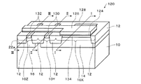
本実施の形態の半導体装置に含まれるメモリセル120は、コントロールゲートが半導体層10内のN型の不純物領域であり、フローティングゲート電極が、一層のポリシリコン層などの導電層からなる(以下、「一層ゲート型の不揮発性記憶装置」ということもある)。図3は、メモリセルを示す斜視図であり、図4(A)は、図3のI−I線に沿った断面図であり、図3(B)は、図3のII−IIに沿った断面図であり、図4(C)は、図3のIII―III線に沿った断面図である。
In the
図3に示すように、本実施の形態におけるメモリセル120は、P型の半導体層10に設けられている。半導体層10は、素子分離絶縁層12により、第1領域10Xと、第2領域10Yと、第3領域10Zとに分離画定されている。第1領域10Xおよび第2領域10Yは、P型のウエル14に設けられている。第3領域10Zは、N型のウエル16に設けられている。第1領域10Xはコントロールゲート部であり、第2領域10Yは書き込み部であり、第3領域10Zは消去部である。
As shown in FIG. 3, the
第1領域10X〜第3領域10Zの半導体層10の上には、絶縁層124が設けられている。絶縁層124の上には、第1〜第3領域10X〜Zにわたって設けられたフローティングゲート電極126が設けられている。
An insulating
次に、各領域の断面構造について説明する。図4(A)に示すように、第1領域10Xでは、ウエル14の上に設けられた絶縁層124と、絶縁層124の上に設けられたフローティングゲート電極126と、フローティングゲート電極126下の半導体10に設けられたN型の不純物領域134と、不純物領域134に隣接して設けられたN型の不純物領域128と、を有する。N型の不純物領域134は、コントロールゲートの役割を果たし、不純物領域128は、コントロールゲート線と電気的に接続され、コントロールゲートに電圧を印加するためのコンタクト部となる。
Next, the cross-sectional structure of each region will be described. As shown in FIG. 4A, in the
図4(B)に示すように、第2領域10Yには、メモリセル120に書き込みを行うためにNチャネル型MOSトランジスタ100Bが設けられている。Nチャネル型トランジスタ100Bは、ウエル14の上に設けられた絶縁層124と、絶縁層124の上に設けられたフローティングゲート電極126と、半導体層10に設けられた不純物領域130と、を有する。不純物領域130は、ソース領域またはドレイン領域となる。
As shown in FIG. 4B, an N-
図4(C)に示すように、第3領域10Zには、Pチャネル型トランジスタ100Cが設けられている。Pチャネル型トランジスタ100Cは、N型のウエル16の上に設けられた絶縁層124と、絶縁層124の上に設けられたフローティングゲート電極126と、N型のウエル16に設けられた不純物領域132とを有する。不純物領域132は、ソース領域またはドレイン領域となる。
As shown in FIG. 4C, a P-
ついで、図5を参照しつつ、本実施の形態の半導体装置について説明する。なお、図5では、素子形成領域10Aにおいて、メモリセル120の構成要素のうち、フローティングゲート電極126の形状のみを示すものとする。図5に示すように、素子形成領域10A内には、2つのメモリセル120が設けられている。この素子形成領域10Aを囲むように、遮光壁50が設けられている。遮光壁50は、素子形成領域10Aの周囲をすべて囲んでいるのではなく、第1の実施の形態と同様に開孔52を有する。この開孔52から、メモリセル120の信号線26、27が素子形成領域10Aの外側に引き出されている。信号線26は、第3領域10Zに設けられているPチャネル型トランジスタ100Cと電気的に接続されている。また信号線27は、第1領域10Xの不純物領域128と電気的に接続されている。図5に示す半導体装置では、信号線26、27が同一の方向でかつ一の開孔52から引き出されている場合を示す。
Next, the semiconductor device of the present embodiment will be described with reference to FIG. In FIG. 5, only the shape of the floating
信号線26は、開孔52の位置に設けられている第1部分26Aと、開孔52の内側に位置し、第1部分26Aと比して幅が大きい第2部分26Bとを含むパターンを有している。同様に、信号線27も、第1部分27Aと、開孔52の外側に位置し、第1部分27Aと比して幅が大きい第2部分27Bとを含むパターンを有している。そして、第2部分26Bおよび第2部分27Bの全体の幅Yが、開孔52の幅と重複するように信号線26、27がパターニングされている。本実施の形態では、開孔52の外側のうち、素子形成領域10A側に第2部分26B、27Bが設けられている場合を示す。信号線26、27は、第1の実施の形態と同様に、分岐部28、29を設けることで、信号線26、27の幅が局所的に大きくなるパターンを有している。このように、分岐部28、29が設けられたことにより、第2部分26Bと第2部分27Bとを併合した幅Yを、開孔52の幅Xと比して大きくすることができるのである。
The
次に、第2の実施の形態の半導体装置にかかる断面形状について、図6(A)および図6(B)を参照しつつ説明する。 Next, a cross-sectional shape of the semiconductor device according to the second embodiment will be described with reference to FIGS. 6 (A) and 6 (B).
図6に示すように、半導体装置200では、素子形成領域10Aの半導体層の上に、メモリセル120が設けられている。メモリセル120の具体的な構造については、上述の説明を参照されたい。
As shown in FIG. 6, in the semiconductor device 200, the
図6(A)および図6(B)に示すように、メモリセル120を覆うように半導体層10の上に第1層間絶縁層20および第2層間絶縁層30が順次設けられている。図6(A)に示すように、遮光壁50(図5参照)が設けられない領域、すなわち、開孔52となる領域では、第1層間絶縁層20の上に信号線26が設けられている。信号線26は、メモリセル120の第3領域10ZのPチャネル型トランジスタ100Cと電気的に接続されている。
As shown in FIGS. 6A and 6B, a first
また、図6(B)に示すように、遮光壁50となる領域では、第1層間絶縁層20の上には第1金属層24が、第2層間絶縁層30の上には第2金属層34が設けられている。半導体層10と第1金属層24との間には、コンタクト層22が、第1金属層24と第2金属層34との間にはビア層32が設けられている。コンタクト層22およびビア層32は、第1層間絶縁層20および第2層間絶縁層30に開口22a、32aを設け、この開口22a、32aに導電層を埋め込んで形成された層である。開口22a、32aは、素子形成領域10Aを囲むように形成された溝状の開口である。そのため、コンタクト層22とビア層32の全体が壁状になし、素子形成領域10Aを囲むことになる。
Further, as shown in FIG. 6B, in the region to be the
第2の実施の形態の半導体装置によれば、メモリセル120の周囲には、遮光壁50が設けられているために、横方向または斜め上方向からの光の進入を低減することができる。さらに、メモリセル120と接続された信号線26、27を遮光壁50の開孔52から引き出す際には、第2部分26B、27Bを設けるなど信号線26、27の幅を局所的に大きくすることで、開孔52からの光の進入を低減することができる。その結果、電荷保持特性を挙げることができ、信頼性の向上した半導体装置を提供することができる。
According to the semiconductor device of the second embodiment, since the
(変形例)
次に、第2の実施の形態の変形例にかかる半導体装置を、図7を参照しつつ説明する。図7は、変形例にかかる半導体装置を示す平面図であり、図5に対応する平面を示す。
(Modification)
Next, a semiconductor device according to a modification of the second embodiment will be described with reference to FIG. FIG. 7 is a plan view showing a semiconductor device according to a modification, and shows a plane corresponding to FIG.
変形例にかかる半導体装置は、図7に示すように、信号線26と信号線27との引き出す方向が異なる。つまり、遮光壁50が設けられていない箇所、すなわち開孔52、54が、それぞれ素子形成領域10Aの異なる辺に設けられている。開孔52からは信号線26が、開孔54からは信号線27がそれぞれ引き出されている。信号線26、27は、それぞれ、開孔52、54の幅以上の幅を有する第2部分26B、27Bを含むパターンを有している。そのため、横方向および斜め方向からの光の侵入を低減することができ、その結果、電荷保持特性が向上した半導体装置を提供することができる。
As shown in FIG. 7, the semiconductor device according to the modification differs in the direction in which the
3.第3の実施の形態
次に、第3の実施の形態にかかる半導体装置について、図8、9を参照しつつ説明する。図8は、第3の実施の形態にかかる半導体装置を模式的に示す平面図であり、図5に対応した平面を示す図である。図9は、図8のA部を拡大して示す平面図である。図8に示すように、第3の実施の形態にかかる半導体装置は、上述の実施の形態にかかる半導体装置と比して第2部分26Bの形状が異なる例である。以下の説明では、上述の実施の形態と共通する構造については、詳細な説明は省略する。
3. Third Embodiment Next, a semiconductor device according to a third embodiment will be described with reference to FIGS. FIG. 8 is a plan view schematically showing a semiconductor device according to the third embodiment, and shows a plane corresponding to FIG. FIG. 9 is an enlarged plan view showing a portion A of FIG. As shown in FIG. 8, the semiconductor device according to the third embodiment is an example in which the shape of the
図8に示すように、素子形成領域10Aにメモリセル120が設けられている。素子形成領域10Aは、その周囲が遮光壁50によりに覆われている。メモリセル120に電気的に接続されている信号線26、27は、遮光壁50が設けられていない開孔52から、遮光壁50の外側に引き出されている。信号線26、27は、開孔52の外側に、分岐部28、29を有している。図9に示すように、第3の実施の形態にかかる半導体装置では、この分岐部28、29の側面のうち光が進入してくる方向を向いた面は、その表面に凸部28a、29aを有している。凸部28a、29aとして、分岐部28、29の側面において、面の高さを不均一にできる形状であれば特に制限はなく、たとえば、凸部の先端が曲面を有していてもよい。好ましい凸部28a、29aの形状としては、複数の斜面からなる尖鋭形状を挙げることができる。図8、9には、2つの斜面からなる尖鋭形状の凸部28a、29aがライン状に設けられている場合を示す。
As shown in FIG. 8, a
第3の実施の形態の半導体装置によれば、開孔52の外側に位置している第2部分26B、27Bにおいて、光の進入方向と対向する側面(つまり分岐部28、29の側面)は、その表面に凸部28a、29aを有している。そのため、開孔52に進入してくる光の入射角の大小にかかわらず、その光を反射させることができ、光の進入のさらなる低減を図ることができる。その結果、特性の変動が抑制され、信頼性の向上した半導体装置を提供することができる。また、凸部28a、29aが尖鋭形状からなる場合には、開孔52に向って斜め方向から進入してくる光を容易に反射させることができる。
According to the semiconductor device of the third embodiment, in the
4.第4の実施の形態
図10は、第4の実施の形態にかかる半導体装置を模式的に示す平面図であり、図9に対応した平面を示す図である。図10に示すように、第4の実施の形態にかかる半導体装置は、上述の実施の形態にかかる半導体装置と比して第2部分の形状が異なる例である。以下の説明では、上述の実施の形態と共通する構造については、詳細な説明は省略する。
4). Fourth Embodiment FIG. 10 is a plan view schematically showing a semiconductor device according to a fourth embodiment, and is a diagram showing a plane corresponding to FIG. As shown in FIG. 10, the semiconductor device according to the fourth embodiment is an example in which the shape of the second portion is different from that of the semiconductor device according to the above-described embodiment. In the following description, detailed description of structures common to the above-described embodiments is omitted.
図10に示すように、第4の実施の形態にかかる半導体装置では、第2部分26Bは、光の進入方向に向かって凹形状を有している。具体的には、第2部分26Bは、分岐部28を含んで構成されるが、この分岐部29は、軸である信号線26からの距離が大きくなるにつれて、つまり分岐部28の先端方向に向かって、その長さZが大きくなるような形状を有している。そのため、第2部分26Bの全体的な形状は、光の進入方向に向かって凹形状の曲面を有することになるのである。
As shown in FIG. 10, in the semiconductor device according to the fourth embodiment, the
第4の実施の形態の半導体装置によれば、上述の他の実施の形態と同様の利点を有し、横方向または斜め上方向からの光の進入を低減することができる。さらに、第2部分26Bは、光の進入方向対して凹状の曲面を有している。そのため、開孔52に向かって斜め上方向から進入する光であっても反射させることができ、光の進入のさらなる低減を図ることができる。その結果、特性の変動が抑制され、信頼性の向上した半導体装置を提供することができる。
The semiconductor device according to the fourth embodiment has the same advantages as those of the other embodiments described above, and can reduce the ingress of light from the lateral direction or obliquely upward. Further, the
5.第5の実施の形態
図11は、第5の実施の形態にかかる半導体装置を模式的に示す平面図であり、図9に対応した平面を示す図である。図11に示すように、第5の実施の形態にかかる半導体装置は、上述の実施の形態にかかる半導体装置と比して第2部分の形状が異なる例である。以下の説明では、上述の実施の形態と共通する構造については、詳細な説明は省略する。
5. Fifth Embodiment FIG. 11 is a plan view schematically showing a semiconductor device according to a fifth embodiment, and shows a plane corresponding to FIG. As shown in FIG. 11, the semiconductor device according to the fifth embodiment is an example in which the shape of the second portion is different from that of the semiconductor device according to the above-described embodiment. In the following description, detailed description of structures common to the above-described embodiments is omitted.
図11に示すように、第5の実施の形態にかかる半導体装置では、第2部分26Bは、光が進入してくる方向に向かって凹形状を有している。たとえば、図11に示すように、分岐部28、29の形状をL字形状にすることで、第2部分26Bの全体形状を、凹状にすることができる。
As shown in FIG. 11, in the semiconductor device according to the fifth embodiment, the
第5の実施の形態の半導体装置によれば、上述の他の実施の形態と同様の利点を有し、横方向または斜め上方向からの光の進入を低減することができる。 The semiconductor device according to the fifth embodiment has the same advantages as those of the other embodiments described above, and can reduce the entry of light from the lateral direction or obliquely upward.
なお、本発明は、上述の実施の形態に限定されることなく、本発明の要旨の範囲内で変形が可能である。たとえば、本実施の形態では、半導体素子の上方に第1層間絶縁層20および第2層間絶縁層30の2層が設けられている場合を図示したが、これに限定されず、3層以上の複数の層間絶縁層が設けられていてもよい。この場合は、各層間絶縁層において、素子形成領域を囲む位置に設けられるビア層が遮光壁を構成することになる。
The present invention is not limited to the above-described embodiment, and can be modified within the scope of the gist of the present invention. For example, in the present embodiment, the case where two layers of the first
また、本実施の形態では、遮光壁50を構成するビア層32やコンタクト層22の位置が重ならないように設けた場合を図示したが、これに限定されず、重なっていてもよい。また、コンタクト層22およびビア層32に代わり、第1層間絶縁層20および第2層間絶縁層30を貫通する開口を設け、この開口に導電材料を埋め込んで遮光壁50とすることもできる。
In the present embodiment, the case where the via
また、図5には、信号線26と信号線27とが、1つの開孔52から引き出されている場合を図示したが、これに限定されず、それぞれの信号線26、27のために開孔を設ける態様をとることもできる。
FIG. 5 shows the case where the
また、上述の実施の形態の半導体装置では、特に素子形成領域10Aの上方を覆う遮光膜を設ける場合を図示しなかったが、素子形成領域10Aの上方に遮光膜を設けることが好ましいのはいうまでもない。この態様では、上方向および横方向からの光の進入を低減でき、さらに、信頼性の向上した半導体装置を提供することができる。
Further, in the semiconductor device of the above-described embodiment, a case where a light shielding film covering the
10…半導体層、 10A…素子形成領域、 10X…第1領域、 10Y…第2領域、 10Z…第3領域、 12…素子分離絶縁層、 16…ウエル、 20…第1層間絶縁層、 22…コンタクト層、 24…第1金属層、 26、27…配線層(信号線)、 26A…第1部分、 26B…第2部分、 27…信号線、 28、29…分岐部、 28a、29a…凸部、 30…第2層間絶縁層、 32…ビア層、 22a、32a…開口部、 34…第2金属層、 50…遮光壁、 52、54…開孔、 120…メモリセル
DESCRIPTION OF
Claims (16)
前記半導体素子の周囲に設けられ、開孔を有する遮光壁と、
前記半導体素子に電気的に接続された配線層であって、前記開孔から前記遮光壁の外側に延伸された配線層と、を含み、
前記配線層は、前記開孔に位置している第1部分と、前記遮光壁に囲まれた領域以外に位置し該第1部分と比して大きい幅を有する第2部分と、を含むパターンを有し、
前記第2部分は、前記開孔の幅と同一以上の幅を有する、半導体装置。 A semi-conductor element,
A light shielding wall provided around the semiconductor element and having an aperture ;
Wherein a wiring layer electrically connected to the semiconductor element, wherein the wiring layer which is stretched on the outside of the shielding wall from said opening,
The wiring layer includes a first portion located in the opening and a second portion located outside the region surrounded by the light shielding wall and having a larger width than the first portion. Have
The semiconductor device, wherein the second portion has a width equal to or greater than a width of the opening.
前記第1部分が延伸している方向からみたときに、前記第2部分は、少なくとも前記開孔と重なるように設けられている、半導体装置。 In claim 1,
When the first portion is viewed from a direction that extends, the second portion is provided so as to overlap with at least the aperture, the semiconductor device.
前記第2部分は、前記第1部分が延伸した方向を軸として該軸と交差する方向に分岐した分岐部を含む、半導体装置。 In claim 1 or 2,
The second portion includes a branching portion that branches in a direction intersecting the axis with the direction in which the first portion extends as an axis.
前記第2部分は、前記第1部分が延伸した方向を軸として該軸と直角の方向に延在している、半導体装置。The semiconductor device, wherein the second part extends in a direction perpendicular to the axis with the direction in which the first part extends as an axis.
前記第2部分は、前記半導体素子の位置を前記遮光壁の内側とした場合、前記遮光壁に囲まれた領域の外側に設けられている、半導体装置。 In any of claims 1 to 4 ,
The second portion is a semiconductor device provided outside the region surrounded by the light shielding wall when the position of the semiconductor element is located inside the light shielding wall.
さらに、前記半導体素子の上方に設けられた遮光膜を含む、半導体装置。 In any of claims 1 to 5,
Furthermore, the semiconductor device containing the light shielding film provided above the said semiconductor element.
前記遮光壁は、
前記半導体素子の上方に設けられた層間絶縁層と、
前記層間絶縁層に設けられた溝と、
前記溝に埋め込まれた遮光材料と、を含む、半導体装置。 In any one of Claims 1 thru | or 6.
The light shielding wall is
An interlayer insulating layer provided above the semiconductor element;
A groove provided in the interlayer insulating layer;
And a light shielding material embedded in the groove.
前記半導体素子は、
フローティングゲート電極を有する不揮発性メモリである、半導体装置。 In any one of Claims 1 thru | or 7,
The semiconductor element is
A semiconductor device, which is a nonvolatile memory having a floating gate electrode.
前記不揮発性メモリは、単層ゲート型の不揮発性メモリである、半導体装置。 In claim 8,
The nonvolatile memory is a semiconductor device which is a single-layer gate nonvolatile memory.
前記配線層は、信号線である、半導体装置。 In any one of Claim 1 thru | or 9 ,
The semiconductor device, wherein the wiring layer is a signal line.
さらに、半導体層を含み、Furthermore, including a semiconductor layer,
前記配線層は、前記半導体層の上方に設けられている、半導体装置。The semiconductor device, wherein the wiring layer is provided above the semiconductor layer.
前記半導体素子は、トランジスタである、半導体装置。The semiconductor device, wherein the semiconductor element is a transistor.
前記第2部分の幅は、前記遮光壁の一辺よりも小さい、半導体装置。The width of the second portion is a semiconductor device smaller than one side of the light shielding wall.
前記遮光材料は、導電層である、半導体装置。The semiconductor device, wherein the light shielding material is a conductive layer.
前記導電層は、金属層である、半導体装置。The semiconductor device, wherein the conductive layer is a metal layer.
前記第2部分によって、前記開孔から前記遮光壁に囲まれた領域への光の進入が低減されている、半導体装置。The semiconductor device, wherein the second portion reduces light intrusion from the opening to a region surrounded by the light shielding wall.
Priority Applications (5)
| Application Number | Priority Date | Filing Date | Title |
|---|---|---|---|
| JP2004369587A JP4099672B2 (en) | 2004-12-21 | 2004-12-21 | Semiconductor device |
| US11/249,253 US7253462B2 (en) | 2004-12-21 | 2005-10-13 | Semiconductor device |
| US11/768,514 US7482647B2 (en) | 2004-12-21 | 2007-06-26 | Semiconductor device |
| US11/768,589 US7508019B2 (en) | 2004-12-21 | 2007-06-26 | Semiconductor device |
| US11/768,387 US7612396B2 (en) | 2004-12-21 | 2007-06-26 | Semiconductor device |
Applications Claiming Priority (1)
| Application Number | Priority Date | Filing Date | Title |
|---|---|---|---|
| JP2004369587A JP4099672B2 (en) | 2004-12-21 | 2004-12-21 | Semiconductor device |
Related Child Applications (3)
| Application Number | Title | Priority Date | Filing Date |
|---|---|---|---|
| JP2008016013A Division JP4735864B2 (en) | 2008-01-28 | 2008-01-28 | Semiconductor device |
| JP2008016012A Division JP4766277B2 (en) | 2008-01-28 | 2008-01-28 | Semiconductor device |
| JP2008016011A Division JP4735863B2 (en) | 2008-01-28 | 2008-01-28 | Semiconductor device |
Publications (2)
| Publication Number | Publication Date |
|---|---|
| JP2006179590A JP2006179590A (en) | 2006-07-06 |
| JP4099672B2 true JP4099672B2 (en) | 2008-06-11 |
Family
ID=36594574
Family Applications (1)
| Application Number | Title | Priority Date | Filing Date |
|---|---|---|---|
| JP2004369587A Active JP4099672B2 (en) | 2004-12-21 | 2004-12-21 | Semiconductor device |
Country Status (2)
| Country | Link |
|---|---|
| US (4) | US7253462B2 (en) |
| JP (1) | JP4099672B2 (en) |
Cited By (1)
| Publication number | Priority date | Publication date | Assignee | Title |
|---|---|---|---|---|
| JP2006295046A (en) * | 2005-04-14 | 2006-10-26 | Seiko Epson Corp | Semiconductor device |
Families Citing this family (7)
| Publication number | Priority date | Publication date | Assignee | Title |
|---|---|---|---|---|
| JP4626373B2 (en) * | 2005-04-14 | 2011-02-09 | セイコーエプソン株式会社 | Semiconductor device |
| KR101427581B1 (en) * | 2007-11-09 | 2014-08-07 | 삼성디스플레이 주식회사 | Organic light emitting diode display and method for manufacturing the same |
| JP4766277B2 (en) * | 2008-01-28 | 2011-09-07 | セイコーエプソン株式会社 | Semiconductor device |
| JP4735864B2 (en) * | 2008-01-28 | 2011-07-27 | セイコーエプソン株式会社 | Semiconductor device |
| JP4735863B2 (en) * | 2008-01-28 | 2011-07-27 | セイコーエプソン株式会社 | Semiconductor device |
| US8708697B2 (en) | 2009-12-08 | 2014-04-29 | Align Technology, Inc. | Tactile objects for orthodontics, systems and methods |
| US7999361B1 (en) * | 2010-02-19 | 2011-08-16 | Altera Corporation | Shielding structure for transmission lines |
Family Cites Families (22)
| Publication number | Priority date | Publication date | Assignee | Title |
|---|---|---|---|---|
| JPS61129875A (en) | 1984-11-28 | 1986-06-17 | Seiko Epson Corp | Semiconductor device |
| JPS63308388A (en) | 1987-06-10 | 1988-12-15 | Mitsubishi Electric Corp | Semiconductor storage device |
| JPS63310180A (en) | 1987-06-11 | 1988-12-19 | Mitsubishi Electric Corp | Semiconductor memory device |
| JPH01117375A (en) * | 1987-10-30 | 1989-05-10 | Hamamatsu Photonics Kk | Semiconductor device |
| JPH04321273A (en) * | 1991-04-19 | 1992-11-11 | Fuji Xerox Co Ltd | Image sensor |
| US5525827A (en) * | 1993-11-05 | 1996-06-11 | Norman; Kevin A. | Unerasable electronic programmable read only memory (UPROM™) |
| US5736756A (en) * | 1994-09-29 | 1998-04-07 | Sony Corporation | Solid-state image sensing device with lght shielding film |
| US6266110B1 (en) * | 1996-07-30 | 2001-07-24 | Kawasaki Steel Corporation | Semiconductor device reeventing light from entering its substrate transistor and the same for driving reflection type liquid crystal |
| JP3716580B2 (en) * | 1997-02-27 | 2005-11-16 | セイコーエプソン株式会社 | Liquid crystal device and manufacturing method thereof, and projection display device |
| JPH1113979A (en) * | 1997-06-26 | 1999-01-22 | Kitz Corp | Electrically fused joint and its fixing method |
| US6166403A (en) * | 1997-11-12 | 2000-12-26 | Lsi Logic Corporation | Integrated circuit having embedded memory with electromagnetic shield |
| JP3601761B2 (en) * | 1998-11-19 | 2004-12-15 | 松下電器産業株式会社 | Light receiving element and method of manufacturing the same |
| JP4700156B2 (en) * | 1999-09-27 | 2011-06-15 | 株式会社半導体エネルギー研究所 | Semiconductor device |
| JP3478768B2 (en) * | 1999-10-04 | 2003-12-15 | 三洋電機株式会社 | Semiconductor device |
| JP2001354968A (en) * | 2000-06-09 | 2001-12-25 | Hitachi Ltd | Active matrix liquid crystal display device and its liquid crystal composition substance |
| US6653617B2 (en) * | 2000-07-03 | 2003-11-25 | Canon Kabushiki Kaisha | Photoelectric conversion device |
| JP2003124363A (en) | 2001-10-19 | 2003-04-25 | Toshiba Corp | Semiconductor memory |
| JP3928543B2 (en) * | 2001-12-11 | 2007-06-13 | セイコーエプソン株式会社 | Electro-optical device substrate and method for manufacturing the same, electro-optical device, and electronic apparatus |
| US6956281B2 (en) * | 2002-08-21 | 2005-10-18 | Freescale Semiconductor, Inc. | Semiconductor device for reducing photovolatic current |
| JP2004104203A (en) * | 2002-09-05 | 2004-04-02 | Toshiba Corp | Solid state imaging device |
| JP3794411B2 (en) * | 2003-03-14 | 2006-07-05 | セイコーエプソン株式会社 | Display device and electronic device |
| JP4274118B2 (en) * | 2004-12-27 | 2009-06-03 | セイコーエプソン株式会社 | Semiconductor device |
-
2004
- 2004-12-21 JP JP2004369587A patent/JP4099672B2/en active Active
-
2005
- 2005-10-13 US US11/249,253 patent/US7253462B2/en active Active
-
2007
- 2007-06-26 US US11/768,387 patent/US7612396B2/en not_active Expired - Fee Related
- 2007-06-26 US US11/768,589 patent/US7508019B2/en not_active Expired - Fee Related
- 2007-06-26 US US11/768,514 patent/US7482647B2/en not_active Expired - Fee Related
Cited By (1)
| Publication number | Priority date | Publication date | Assignee | Title |
|---|---|---|---|---|
| JP2006295046A (en) * | 2005-04-14 | 2006-10-26 | Seiko Epson Corp | Semiconductor device |
Also Published As
| Publication number | Publication date |
|---|---|
| US7508019B2 (en) | 2009-03-24 |
| US20060131626A1 (en) | 2006-06-22 |
| US7482647B2 (en) | 2009-01-27 |
| US20070246758A1 (en) | 2007-10-25 |
| US7612396B2 (en) | 2009-11-03 |
| US7253462B2 (en) | 2007-08-07 |
| JP2006179590A (en) | 2006-07-06 |
| US20070246760A1 (en) | 2007-10-25 |
| US20070246759A1 (en) | 2007-10-25 |
Similar Documents
| Publication | Publication Date | Title |
|---|---|---|
| US7612396B2 (en) | Semiconductor device | |
| US7667249B2 (en) | Semiconductor device | |
| KR100718622B1 (en) | Semiconductor device | |
| KR19980070625A (en) | Semiconductor memory | |
| US5107313A (en) | Floating gate type semiconductor memory device | |
| JP4274118B2 (en) | Semiconductor device | |
| JP4735862B2 (en) | Semiconductor device | |
| JP4735864B2 (en) | Semiconductor device | |
| JP4735863B2 (en) | Semiconductor device | |
| JP4766277B2 (en) | Semiconductor device | |
| JP2582412B2 (en) | Nonvolatile semiconductor memory device | |
| JP4858671B2 (en) | Semiconductor device | |
| JP4952954B2 (en) | Semiconductor device | |
| JP2009076933A (en) | Semiconductor device | |
| US6818942B2 (en) | Non-volatile semiconductor storage device having conductive layer surrounding floating gate | |
| JP5467761B2 (en) | EEPROM | |
| JP4548603B2 (en) | Semiconductor device | |
| JP2006216683A (en) | Semiconductor device | |
| KR100486238B1 (en) | Cell array unit of NOR flash memory device | |
| JPH01293670A (en) | Semiconductor memory device |
Legal Events
| Date | Code | Title | Description |
|---|---|---|---|
| A977 | Report on retrieval |
Free format text: JAPANESE INTERMEDIATE CODE: A971007 Effective date: 20071126 |
|
| A131 | Notification of reasons for refusal |
Free format text: JAPANESE INTERMEDIATE CODE: A131 Effective date: 20071128 |
|
| A521 | Request for written amendment filed |
Free format text: JAPANESE INTERMEDIATE CODE: A523 Effective date: 20080128 |
|
| TRDD | Decision of grant or rejection written | ||
| A01 | Written decision to grant a patent or to grant a registration (utility model) |
Free format text: JAPANESE INTERMEDIATE CODE: A01 Effective date: 20080220 |
|
| A61 | First payment of annual fees (during grant procedure) |
Free format text: JAPANESE INTERMEDIATE CODE: A61 Effective date: 20080304 |
|
| FPAY | Renewal fee payment (event date is renewal date of database) |
Free format text: PAYMENT UNTIL: 20110328 Year of fee payment: 3 |
|
| R150 | Certificate of patent or registration of utility model |
Ref document number: 4099672 Country of ref document: JP Free format text: JAPANESE INTERMEDIATE CODE: R150 Free format text: JAPANESE INTERMEDIATE CODE: R150 |
|
| FPAY | Renewal fee payment (event date is renewal date of database) |
Free format text: PAYMENT UNTIL: 20120328 Year of fee payment: 4 |
|
| FPAY | Renewal fee payment (event date is renewal date of database) |
Free format text: PAYMENT UNTIL: 20120328 Year of fee payment: 4 |
|
| FPAY | Renewal fee payment (event date is renewal date of database) |
Free format text: PAYMENT UNTIL: 20130328 Year of fee payment: 5 |
|
| FPAY | Renewal fee payment (event date is renewal date of database) |
Free format text: PAYMENT UNTIL: 20140328 Year of fee payment: 6 |
|
| S531 | Written request for registration of change of domicile |
Free format text: JAPANESE INTERMEDIATE CODE: R313531 |
|
| R350 | Written notification of registration of transfer |
Free format text: JAPANESE INTERMEDIATE CODE: R350 |