JP4097708B2 - Transponders created for contactless inductive communications - Google Patents
Transponders created for contactless inductive communications Download PDFInfo
- Publication number
- JP4097708B2 JP4097708B2 JP52933998A JP52933998A JP4097708B2 JP 4097708 B2 JP4097708 B2 JP 4097708B2 JP 52933998 A JP52933998 A JP 52933998A JP 52933998 A JP52933998 A JP 52933998A JP 4097708 B2 JP4097708 B2 JP 4097708B2
- Authority
- JP
- Japan
- Prior art keywords
- signal
- transponder
- mode
- frequency
- data
- Prior art date
- Legal status (The legal status is an assumption and is not a legal conclusion. Google has not performed a legal analysis and makes no representation as to the accuracy of the status listed.)
- Expired - Lifetime
Links
Images


Classifications
-
- G—PHYSICS
- G06—COMPUTING; CALCULATING OR COUNTING
- G06K—GRAPHICAL DATA READING; PRESENTATION OF DATA; RECORD CARRIERS; HANDLING RECORD CARRIERS
- G06K19/00—Record carriers for use with machines and with at least a part designed to carry digital markings
- G06K19/06—Record carriers for use with machines and with at least a part designed to carry digital markings characterised by the kind of the digital marking, e.g. shape, nature, code
- G06K19/067—Record carriers with conductive marks, printed circuits or semiconductor circuit elements, e.g. credit or identity cards also with resonating or responding marks without active components
- G06K19/07—Record carriers with conductive marks, printed circuits or semiconductor circuit elements, e.g. credit or identity cards also with resonating or responding marks without active components with integrated circuit chips
- G06K19/077—Constructional details, e.g. mounting of circuits in the carrier
- G06K19/07749—Constructional details, e.g. mounting of circuits in the carrier the record carrier being capable of non-contact communication, e.g. constructional details of the antenna of a non-contact smart card
- G06K19/07773—Antenna details
- G06K19/07777—Antenna details the antenna being of the inductive type
-
- G—PHYSICS
- G06—COMPUTING; CALCULATING OR COUNTING
- G06K—GRAPHICAL DATA READING; PRESENTATION OF DATA; RECORD CARRIERS; HANDLING RECORD CARRIERS
- G06K19/00—Record carriers for use with machines and with at least a part designed to carry digital markings
- G06K19/06—Record carriers for use with machines and with at least a part designed to carry digital markings characterised by the kind of the digital marking, e.g. shape, nature, code
- G06K19/067—Record carriers with conductive marks, printed circuits or semiconductor circuit elements, e.g. credit or identity cards also with resonating or responding marks without active components
- G06K19/07—Record carriers with conductive marks, printed circuits or semiconductor circuit elements, e.g. credit or identity cards also with resonating or responding marks without active components with integrated circuit chips
- G06K19/0723—Record carriers with conductive marks, printed circuits or semiconductor circuit elements, e.g. credit or identity cards also with resonating or responding marks without active components with integrated circuit chips the record carrier comprising an arrangement for non-contact communication, e.g. wireless communication circuits on transponder cards, non-contact smart cards or RFIDs
-
- G—PHYSICS
- G06—COMPUTING; CALCULATING OR COUNTING
- G06K—GRAPHICAL DATA READING; PRESENTATION OF DATA; RECORD CARRIERS; HANDLING RECORD CARRIERS
- G06K7/00—Methods or arrangements for sensing record carriers, e.g. for reading patterns
- G06K7/0008—General problems related to the reading of electronic memory record carriers, independent of its reading method, e.g. power transfer
Abstract
Description
本発明は、基地局と非接触誘導通信をするためのトランスポンダであって、
前記基地局から供給される変調HF信号を受信するとともに、前記信号を信号処理手段に供給するように適合したアンテナ共振回路を具え、
前記信号処理手段が、受信した変調HF信号を処理するとともに、データ信号及びクロック信号を発生し、前記データ信号が、前記変調HF信号に含まれるデータを具え、クロック信号の周波数が、前記HF信号の周波数から取得され、
前記データ処理手段が、前記データ信号及び前記クロック信号を受信するように配置されるとともに、前記データ信号を処理するように適合され、前記データ処理手段の処理速度が、前記クロック信号に依存し、前記データ処理手段が、前記データ信号の処理を終了するリセット情報を受信するよう配置されたトランスポンダに関する。
さらに、本発明は、基地局と非接触誘導通信をするよう構成されたトランスポンダを実現する集積回路であって、
前記基地局から供給される変調HF信号を受信するとともに、前記信号を信号処理手段に供給するように適合したアンテナ共振回路を具え、
前記信号処理手段が、受信した変調HF信号を処理するとともに、データ信号及びクロック信号を発生し、前記データ信号が、前記変調HF信号に含まれるデータを具え、クロック信号の周波数が、前記HF信号の周波数から取得され、
前記データ処理手段が、前記データ信号及び前記クロック信号を受信するように配置されるとともに、前記データ信号を処理するように適合され、前記データ処理手段の処理速度が、前記クロック信号に依存し、前記データ処理手段が、前記データ信号の処理を終了するリセット情報を受信するよう配置された集積回路に関する。
冒頭のパラグラフで定義される形式のトランスポンダ及び次の第2パラグラフで定義される形式の集積回路は、例えば米国特許明細書第US 5,345,231 A号から既知である。該既知のトランスポンダは変調されHF信号を介しての非接触誘導通信のためにアンテナ共振回路と動作リンクを持つアンテナ共振回路を有する。変調されたHF信号は基地局の手段により発生され動作周波数を持つ。
基地局の動作中にトランスポンダのアンテナ共振回路に発生する受信された変調されているHF信号は、受信したHF信号からトランスポンダ中に存在する電力供給の階程に対して直流電圧を導き出す電力供給階程に加えられる。この電力供給階程は、トランスポンダの動作およびデータ信号の処理を終了するために、トランスポンダの信頼できる動作を保証する最低電圧以下に前記電圧が低下する時にトランスポンダ中の階程にリセット情報を供給するリセット階程を更に含む。
トランスポンダの受信モードにおいて、受信された変調されているHF信号は、HF信号の周波数を持つクロック信号を発生するのに適合した信号処理手段に加えられることができる。このクロック信号はマイクロコンピュータで構成されるデータ処理手段に加えられることができ、システム・クロック従って該データ処理手段内の処理速度を規定するので、該データ処理手段中の処理速度は該クロック信号に依存する。
更に、信号処理手段は、受信された変調されているHF信号を復調し且つデータ信号をデータ処理手段へ供給するように適合されている。データ処理モードにおいて、該データ処理手段はデータ信号中に表れるディジタル・データを処理でき、次いでこの処理されたデータはメモリに蓄積され、その結果すでにメモリに蓄積されているデータが変更されることになる。
トランスポンダの送信モードにおいて、データ処理手段により処理されるディジタル信号は信号処理手段にデータ信号として供給されることができる。この信号処理手段は、トランスポンダのアンテナ共振回路および基地局のアンテナ共振回路を経て非変調のHF信号の負荷変調(load modulation)を発生し、それによりトランスポンダにおいて処理されるディジタル・データを誘導的に非接触方法により基地局へ送信することを可能にする。
基地局からトランスポンダへ及びトランスポンダから基地局へ送信され、且つ該トランスポンダのメモリに蓄積されるデータは、例えば金額を示し権限を有する人によってのみ変更されるべきセキュリティに関連したデータであるのが大部分である。基地局において、その種のセキュリティに関連したデータはディジタル鍵の手段により符号化され、既知のトランスポンダに送信後このトランスポンダのデータ処理手段においてトランスポンダのメモリに蓄積されているディジタル鍵の手段により復号化されるので、高度のデータ・セキュリティが達成される。
新規の測定技術の最近の発展に起因して、動作周波数に比較して低い周波数がトランスポンダに送信され、その結果データ処理手段は比較的低い処理速度を持つ、トランスポンダに対して実行される複雑ではあるが可能な測定過程の手段により、トランスポンダ内において非符号化の形態で利用でき、且つこの処理の間、導電性接続を介してトランスポンダのデータ処理手段とメモリの間を伝送されるセキュリティに関連したデータは、前記の導電性接続を利用して、ある環境下で検出されることができる。その種の測定過程は、その種のセキュリティに関連したデータを検出する権限を与えられていない人間により許可なしに実行されることも可能である。この最近の発展の結果、セキュリティに関連したデータに対しての望ましい高度のデータ・セキュリティは、非接触通信のための既知のトランスポンダの手段によっては、最早や十分なレベルの信頼性を持っては達成できなくなり、好ましくない結果となっている。
本発明の目的は、冒頭のパラグラフに定義するタイプのトランスポンダ及び第2パラグラフに定義するタイプの集積回路が持つ上記の問題を除去し、トランスポンダと基地局間の通信過程中に高度のデータ・セキュリティがトランスポンダと基地局間でのセキュリティに関連したデータの送信中および該トランスポンダにおけるセキュリティに関連したデータの処理中の双方で達成されるところの改善されたトランスポンダおよび改善された集積回路を提供することである。
本発明によれば、冒頭のパラグラフに定義されるタイプのトランスポンダでこの目的を達成するために、前記トランスポンダが、前記クロック信号を受信するように配置された周波数検出器を具え、
前記周波数検出器が、前記クロック信号の周波数及び少なくとも一つの限界周波数を比較するように適合され、
前記周波数検出器が、前記リセット情報を発生し、前記クロック信号の流派数が前記限界周波数より低い場合には前記リセット情報を前記データ処理手段に供給するように適合される。
この方法により、データ処理手段内におけるデータ処理は、トランスポンダ中での処理速度が周波数検知器の遮断周波数により規定される与えられた値以下に低下する時に、終了されることが達成される。このようにして、本発明によって例えばディジタル鍵そのもののみでなくその他のいかなるセキュリティに関連したデータのようなトランスポンダのデータ処理手段とメモリ間で伝送されるセキュリティに関連したデータは、測定過程がセキュリティに関連したデータを検出するためにメモリとデータ処理手段の間の導電性の接続上において実行できるが、そのような測定はいかなる有効な測定結果も生じることは殆どないような高速処理速度によってのみ、前記接続を介してトランスポンダのメモリとデータ伝送手段の間を伝送される。
請求項1において定義される特徴を持つ本発明によるトランスポンダにおいて、更に関連する請求項2に定義される手段が取り入れられれば、有利であることが明らかにされた。例えば、もしセキュリティに関連したデータが処理される与えられたモードの動作がトランスポンダ中でアクティブであれば、周波数検出器は限界周波数を規定するように順応し、その結果、この与えられたモードの動作に対する特別な即ち高度のデータ・セキュリティがトランスポンダ内で保証されることが有利に達成される。セキュリティに関連したデータが処理されない他のモードの動作に対して、限界周波数、従って広範な周波数領域における安定したトラブルフリーの通信の長所に対しての特別な即ち高度のデータ・セキュリティを定義する必要はない。複数の異なるモードの動作が活性化されるような本発明によるトランスポンダにおいて、これらのモードのそれぞれの動作に対して与えられたデータ・セキュリティレベルがトランスポンダ内で保証できるように、周波数検出器のこれらの異なるモードの動作に異なる限界周波数を定義することも可能である。
請求項2において定義される特徴を持つ本発明によるトランスポンダにおいて、更に関連する請求項3に定義される手段が取り入れられれば、有利であることが明らかにされた。例えば、トランスポンダが、トランスポンダのメモリから読み出されるか又はメモリに読み込まれる特にセキュリティに関連したデータがデータ処理手段により処理される高セキュリティモードでアクティブである時に、第2限界周波数により規定される特別に高度のデータ・セキュリティレベルが得られ、その結果上記のセキュリティに関連したデータの許可されていない検出を行う目的のためにトランスポンダのデータ処理手段とメモリの間の導電性接続上で実行される測定過程の結果は、いかなる有効な測定結果も生じないので、上記のセキュリティに関連したデータの検出は殆ど不可能であり、従って高度のデータ・セキュリティが保証されることが有利に達成される。一方、トランスポンダが基地局と通信するように配置され且つセキュリティに関連したデータが該トランスポンダ内に既に符号化された形態で利用できるセキュリティモードがトランスポンダ内でアクティブである時に、第1限界周波数により規定され且つ高セキュリティモードにおけるデータ・セキュリティレベルよりは低いが希望するデータ・セキュリティに対して適切であるデータ・セキュリティレベルが得られるが、これはデータ処理手段の低速の処理速度または基地局との通信のための変調された種類に対して殆ど制約が課せられない特長を有する。
請求項3において定義される特徴を持つ本発明によるトランスポンダにおいて、更に関連する請求項4に定義される手段が取り入れられれば、有利であることが明らかにされた。例えば、セキュリティモードがアクティブであれば、トランスポンダの基地局との通信は送信されるべきデータを運ぶHF信号の高度の雑音耐力を持つパルス・スペーシング符号化を使用して可能であることと、更に満足できるデータ・セキュリティレベルが通信中トランスポンダに保証されることが有利に達成される。更に第1限界周波数はパルス・スペース符号化HF信号の基本波の周波数より低い周波数であるので、周波数検知器はパルス・スペーシング符号化されたHF信号の基本波の周波数がトランスポンダのクロック信号中にも表れる事実にも関わらずリセット情報を発生しないことが達成される。この結果、データ処理手段内でのデータ信号の処理はトランスポンダによるパルス・スペーシング符号化されたHF信号の受信中においても終了されることはない。
請求項4において定義される特徴を持つ本発明によるトランスポンダにおいて、更に関連する請求項5に定義される手段が取り入れられれば、有利であることが明らかにされた。例えば、トランスポンダがパルス・スペーシング符号化されたHF信号の受信に適合されている状態において、該トランスポンダがデータ・セキュリティモードに関しアクティブである時に、セキュリティモードより一層高度のデータ・セキュリティレベルを保証する高度セキュリティモードがパルス・スペーシングにより符号化されているデータシーケンスの最後のデータビットの受信と共に該トランスポンダ内に自動的に活性化されることが有利に達成される。
請求項4において定義される特徴を持つ本発明によるトランスポンダにおいて、更に関連する請求項6に定義される手段が取り入れられれば、有利であることが明らかにされた。例えば、トランスポンダがセキュリティに関連したデータを処理し且つ基地局へ送信することに適合されている状態において、該トランスポンダが高度セキュリティモードに関しアクティブである時に、基地局により送信されるパルス・スペーシング符号化されたHF信号が受信されるセキュリティモードは該トランスポンダ内での送信の終了と共に自動的に活性化されることが有利に達成される。
請求項1において定義される特徴を持つ本発明によるトランスポンダにおいて、更に関連する請求項7に定義される手段が取り入れられれば、有利であることが明らかにされた。例えば、セキュリティに関連したデータが処理され次いでトランスポンダのメモリから導電性接続を介してデータ処理手段へ又はデータ処理手段から導電性接続を介してメモリへ移送される与えられた時間間隔において、高度セキュリティモードがデータ処理手段により活性化されることができ且つセキュリティに関連したデータの処理の終了と共に該データ処理手段はセキュリティモードを活性化するのに適合されることが有利に達成される。これは、それぞれの場合にデータ処理手段が処理に必要なデータ・セキュリティレベルを定義できる有利性を持つ。更に、データ処理手段による高度セキュリティモードの活性化の結果として、トランスポンダ内での高度セキュリティモードがアクティブである合計の時間は短縮できるので、トランスポンダは広い周波数範囲における安定し且つトラブルのない通信が可能なセキュリティモードによって長時間動作する。関連する請求項7による手段は関連する請求項2から6に定義されるトランスポンダにおいても有利に適用できる。
本発明によれば、第2パラグラフに定義されるタイプの集積回路でこの目的を達成するために、前記集積回路が、前記クロック信号を受信するように配置された周波数検出器を具え、
前記周波数検出器が、前記クロック信号の周波数及び少なくとも一つの限界周波数を比較するように適合され、
前記周波数検出器が、前記リセット情報を発生し、前記クロック信号の流派数が前記限界周波数より低い場合には前記リセット情報を前記データ処理手段に供給するように適合される。
このようにして、本発明よるこのような集積回路は、請求項1により定義されるトランスポンダに関連して上に記述された利点に対応する利点を有する。
請求項9ないし請求項14で定義される特徴を持つ集積回路の有利な変形は、本発明によるトランスポンダの好都合な変形で請求項2ないし請求項7に定義される特徴を持つそれらトランスポンダの変形に関連して上に記述された利点に対応する利点を有する。
本発明の上記および更に別の態様は、例示により下記に記述の実施例から明らかになり、且つこれらの実施例を参照して解明されるであろう。
本発明は図に示される実施例を参照して一層詳細に説明されるであろうが、本発明はそれに限定されない。
図1は、これも図1にブロック図の形式で概略図として示されている基地局と非接触誘導通信を行うための本発明によるトランスポンダをブロック図の形式で概略図として示す。
図2は、図1のトランスポンダが基地局と通信中に該トランスポンダのアンテナ共振回路に発生するパルス・スペーシング符号化されたHF信号の信号波形を示す。
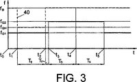
図3は、非変調の基本波およびパルス・スペーシング符号化されたHF信号の周波数値を示すが、これらの周波数値は又ある時間間隔でそのようなパルス・スペーシング符号化されたHF信号を受信する時に図1のトランスポンダに発生するクロック信号においても発生する。更に図1のトランスポンダの周波数検知器により規定される限界周波数の周波数値も示す。
図1は、基地局2との非接触誘導通信のためのトランスポンダ1を示す。基地局2は処理手段3およびアンテナ共振回路4を有する。一般的に知られているように、処理手段3はトランスポンダ1に送信されるべきディジタルデータにより変調されたされることができるHF信号を発生できる。HF信号の変調には、特別に安定で且つ干渉耐力を有するパルス・スペーシング符号化が使用される。
図2は、パルス・スペーシング符号化されたHF信号5の信号波形を示す。HF信号5は動作周波数fBを有する搬送信号7によりHF信号が構成される信号部分6を持つ。HF信号5は、搬送信号が実際上存在せず且つそれぞれがパルススペースを形成する別の信号部分8を持つ。”0”のデータビットは長さTの別の信号部分8と長さ2Tの信号部分6のシーケンスにより符号化される。”1”のデータビットは長さTの別の信号部分6、長さTの別の信号部分8、および長さTの他の別の信号部分6のシーケンスにより符号化される。”0”のデータビットと”1”のデータビットの両方ともに3Tのデータビット長で符号化される。
パルス・スペーシング符号化されたHF信号5は、周波数fGHが方程式
fGH=1/T
を本質的に満足させる第1高調波を持つ。この場合、基本波はパルス・スペーシング符号化されたHF信号5の最低周波数の交流コンポーネントであり、その振幅は実際目的に適した値を持つ。非変調されたHF信号は信号部分6即ち搬送信号7によって全て形成される。非変調されたHF信号の基本波は従って搬送信号7の動作周波数fBを持つ。
基地局2の処理手段3は更にデータ符号で形成される第1ディジタル鍵によりセキュリティに関連したデータを符号化するのに適合される。セキュリティに関連したものは、例えば金銭の額又は許可された人間のみがアクセスできる領域へのアクセス許可を与えるデータであろう。トランスポンダ1のメモリ9は第1ディジタル鍵に対応する第2ディジタル鍵を保持し基地局2により符号化されるセキュリティに関連したデータをトランスポンダ1において復号することを可能にする。セキュリティに関連したデータをディジタル鍵の手段により符号化することは以前から知られてきた。例えば、第1ディジタル鍵と第2ディジタル鍵が同一のいわゆる対称符号化の使用、又は他の方法として2個のディジタル鍵が異なるいわゆる非対称符号化の使用が可能である。
基地局2の送信モードにおいて、パルス・スペーシング符号化されたHF信号5は基地局2の処理手段3からアンテナ共振回路4に供給される。トランスポンダ1も又該トランスポンダ1が基地局2の受信範囲内にある時に該基地局2のアンテナ共振回路4に誘導的に結合するアンテナ共振回路10を持つ。トランスポンダ1のアンテナ共振回路10の手段により基地局2のアンテナ共振回路4に供給される変調されたHF信号5を受信することができる。
トランスポンダ1の受信モードにおいて、アンテナ共振回路10に現れるHF信号5はアンテナ共振回路10のアンテナ端子11からと別のアンテナ端子12から信号処理手段13へ供給できる。信号処理手段13は、変調されたHF信号を処理し且つデータ信号DSおよびクロック信号CLKを供給するように適合され、データ信号DSは変調されたHF信号5に存在するデータを含みクロック信号CLKの周波数はHF信号5に存在する搬送信号7の動作周波数fBから得られる。この目的のために、信号処理手段13は信号準備階程14および処理階程15を含む。
信号準備階程14は、アンテナ共振回路10に接続され且つアンテナ共振回路10に現れるHF信号5を受信するように考慮されたアナログ処理階程16を有する。アナログ処理階程16は、HF信号5の信号対雑音比を強化するためにフイルタ階程と増幅器階程を含むが、このフイルタ階程と増幅器階程は図1には示されていない。アナログ処理階程16において処理されたHF信号5はアナログ処理階程16の出力17で利用できる。
信号準備階程14は、更にアンテナ共振回路10の端子11に接続され且つ端子11に供給されるHF信号5を受信するように配置されたクロック発生階程18を有する。クロック発生階程18はクロック信号CLKを発生するように適合されている。トランスポンダ1が受信モードであり、且つパルス・スペーシング符号化されたHF信号5がクロック発生階程18に加えられる時に、該パルス・スペーシング符号化されたHF信号が長さTのパルス・スペーシングを示す時にクロック信号CLKはタイムインターバルTに対してドロップアウトする。従って、トランスポンダ1が受信モードである時に、パルス・スペーシング符号化されたHF信号5の基本波もクロック信号CLK中に現れる。クロック発生階程18に発生するクロック信号CLKはクロック信号発生階程18のクロック信号出力19において利用できる。
処理階程15はアナログ処理階程16の出力17に接続されている復調階程20を持つ。その信号が信号部分6の搬送信号7および信号部分8のパルス・スペーシングを連続的に有して出力17に現れる処理されたHF信号は、復調階程20に供給される。該復調階程20は更にクロック発生階程18のクロック信号出力19に現れるクロック信号CLKを受信するように考慮されている。復調階程20は、図2に関連して記述された符号化を使用する処理されたHF信号中にパルス・スペーシングが現れる瞬間の検出によりクロック信号CLKの手段によりもたらされる、データビットの検出および復調階程20のバッファ・メモリにそれらを蓄積するように適合されている。復調階程20のバッファ・メモリに与えられた数のデータビットが蓄積される時に、復調階程20は受信制御信号ESを発生し且つこの受信制御信号ESを制御出力21に供給するように適合されている。現在の場合、復調階程20は更にバッファ・メモリに蓄積されるデータビットを該復調階程20の8個のコネクタ接点を持つデータビット・コネクタ22に供給するように適合される。
トランスポンダ1は更にマイクロコンピュータで形成され且つトランスポンダ1のデータ処理モードにあるデータ信号DSを処理するように適合されるデータ処理手段23を含む。この目的のため、該データ処理手段23はクロック発生階程18のクロック信号出力19に接続されるクロック信号入力24を持ち、データ処理手段23のこのクロック信号入力24はクロック信号CLKを受信するように考慮されている。この場合、クロック信号入力24はマイクロコンピュータで形成されるデータ処理手段23においてシステムクロックを形成し、且つデータ処理手段23の処理速度を規定する。
データ処理手段23は、更に同じく8個のコネクタ接点を持ち且つ8個の導電性接続を持つデータバスを介して処理階程15のデータビット・コネクタ22に接続されている、データビット・コネクタ25を含む。データ処理手段23は、更に復調階程20の制御出力21に接続され、且つ該復調階程20からの受信制御信号ESを受信するように考慮されている制御入力26を持つ。受信制御信号ESが現れる時に、データ処理手段23はデータ信号DSを形成し且つデータビット・コネクタ22上で利用できるデータビットを読み出すように適合される。
データ処理モードでデータ処理手段23から読み出されるデータビットは基地局2からトランスポンダ1に送信される符号化されたセキュリティに関連したデータに対応する。該データ処理手段23は、導電性接続27を介して、第2ディジタル鍵を蓄積するメモリ9に接続される。第2ディジタル鍵は、トランスポンダ1へ送信される符号化されたセキュリティに関連したデータを復号するために、接続27を介してメモリ9からデータ処理手段23へ移送される。ディジタルデータ符号で形成される第2ディジタル鍵は、基地局2においてセキュリティに関連したデータが符号化された手段である第1ディジタル鍵に対応する。処理手段23は第2ディジタル鍵の手段により符号化されたセキュリティに関連したデータを復号するのに適合される。
本発明によるトランスポンダ1の適用において、基地局2は銀行の現金自動支払機(ATM)2を形成し、且つトランスポンダ1はICカードの手段により商店で連続する支払いを可能にする金額が電子的に移される非接触誘導通信のためのICカードを形成する。この適用において、金額はデータ処理手段23からメモリ9へ移送される復号されたセキュリティに関連したデータにより表され、且つメモリ9にロードされ得る。
トランスポンダ1のデータ処理モードにおいて、データ処理手段23により処理されるセキュリティに関連したデータは接続27を介してメモリ9からデータ処理手段23へ移送される第2ディジタル鍵の支援の下にデータ処理手段23により符号化され、且つこれらのデータをトランスポンダ1の送信モードに準備するためにデータ処理手段23の別のデータビット・コネクタ25に移送される。データ処理手段23は、更に送信制御信号SSを発生し且つこの送信制御信号SSをデータ処理手段23の制御出力28に供給するように適合される。
信号処理手段13の処理階程15は送信制御信号SSをデータ処理手段23の制御出力28から受信するように考慮された送信信号準備階程29を含む。送信制御信号SSが現れる時に、データ処理手段23の別のデータビット・コネクタ25に加えられるデータビットにより形成されるデータ信号DSは送信信号準備階程29に加えられる。送信信号準備階程29は、加えられたデータビットを直列データビット信号DSBへ処理するのように適合される。該直列データビット信号DSBは信号準備階程14の変調器階程30に加えられる。該変調器階程30は、昔から所謂負荷変調として知られている、受信した直列データビット信号DSBに応じてアンテナ共振回路10に負荷するように適合される。トランスポンダ1が基地局2の受信範囲内に存在する時に、上記の負荷変調は基地局2のアンテナ共振回路4に負荷変調されたHF信号を誘起する。アンテナ共振回路4に誘起される負荷変調されたHF信号はアンテナ共振回路4から処理手段3に供給され、その処理手段3において復調され第1ディジタル鍵の手段により復号される。
トランスポンダ1はクロック発生階程18のクロック信号出力19からクロック信号CLKを受信するように考慮されたクロック信号入力32を持つ周波数検出器31も有する。周波数検出器31は該周波数検出器31のクロック信号入力32からクロック信号CLKを受信するように考慮された比較階程33を有する。
周波数検出器31は、更に第1限界周波数fG1を持つ時刻基本信号ZSを比較階程33に供給するように適合される時刻基本階程34を有する。比較階程33は、クロック信号CLKの周波数を時刻基本信号ZSの第1限界周波数fG1と比較し且つクロック信号CLKの周波数が第1限界周波数fG1より低い時にはリセット情報RIを供給するように適合される。リセット情報RIは周波数検出器31の比較階程33からデータ処理手段23のリセット入力35に供給される。リセット情報RIが発生する時に、データ処理手段23はデータ信号DSの処理を終了するように適合される。周波数検出器31がリセット情報RIをデータ処理手段23へ供給することを停止する時は、該データ処理手段23は、マイクロコンピュータにおいてマイクロコンピュータのリセッティングにおいて一般的であるように、データ信号DSの処理を初期状態から開始させるように適合される。
これは、処理手段23によるデータ信号DSの処理はトランスポンダ1のアンテナ共振回路10に対してその基本波が周波数検出器31により規定される第1限界周波数fG1以下の周波数を持つHF信号が供給される時に終了させられるという長所を持つ。従って、データ処理手段23とメモリ9の間の接続27を介して伝送される非復号のセキュリティに関連したデータを検出するために、接続27上で実施される測定過程はいかなる有効な測定結果を生じることも極めて有りえない。この方法により、本発明によるトランスポンダ1と基地局2の間の通信過程中のデータセキュリティは顕著に改善される。
信号処理手段13の処理階程15は、数種の異なるモード情報信号を発生し且つモード出力37上に供給し、それによりトランスポンダ1内に数種の動作モードを活性化するのに順応するモード階程36を有する。受信モードを特性付けるモード情報信号BIである、データ処理モード、送信モードおよび別の動作モードは、モード出力37からデータ処理手段23および周波数検知器31の時刻基本階程31に加えられる。データ処理手段23は、モード情報信号BIが発生する時に瞬時的動作モードに応じて該データ処理手段23中のデータ信号の処理を活性化するように適合する。周波数検出器31の時刻基本階程34は、モード情報信号BIが発生する時に活性化された動作モードに基づき少なくとも1個の限界周波数を決定するように適合される。これは、周波数検出器31はセキュリティに関連したデータが処理されるデータ処理モードにおいて限界周波数を定義するように適合され、その結果データ処理モードがアクティブの時に非常に高度のデータセキュリティ・レベルが保証されるという特長を持つ。セキュリティに関連したデータが処理されていない他のモードにおいては、広範な周波数レンジにおいて安定且つトラブルフリーの通信の利点のために、周波数検出器31において限界周波数を設定し且つ特別な高度のデータセキュリティ・レベルを保証する必要はない。
モード階程36は、トランスポンダ1が変調されたHF信号を受信するように適合されているセキュリティ・モードを該トランスポンダ1内に活性化するように適合されている。セキュリティ・モードは上記の受信モードに対応しているが、更に、トランスポンダ1内のデータセキュリティ・レベルは周波数検出器31内に第1限界周波数fG1を規定することにより規定されている。モード階程36は、更にトランスポンダ1がセキュリティに関連したデータを処理するように適合されている高度セキュリティ・モードを該トランスポンダ1内に活性化するように適合されている。高度セキュリティ・モードは上記のデータ処理モードに対応していて、もし適用できれば送信モードにも対応するが、更に、与えられた非常に高度のデータセキュリティ・レベルは第2限界周波数fG2が周波数検出器31内に規定されている高度セキュリティ・モードにおいて保証される。これは、セキュリティに関連したデータはトランスポンダ1内において特別に高度のデータセキュリティ・レベルが保証される高度セキュリティ・モードにおいてのみ処理される特長を持つ。しかし、データセキュリティ・レベルはトランスポンダ1のセキュリティ・モードにおいても満足される。
信号処理手段13がアンテナ共振回路10において受信するパルス・スペーシング符号化されたHF信号5を処理するのに適合されているセキュリティ・モードにおいて、周波数検知器31は該パルス・スペーシング符号化されたHF信号5の基本波の周波数より低い周波数において第1限界周波数fG1を規定するように適合される。これは、周波数検知器31が、クロック信号CLKにも現れるリセット情報RIを、パルス・スペーシング符号化されたHF信号5の基本波の周波数より低いクロック信号CLKの周波数においてのみ発生させるという長所を持つ。このようにして、パルス・スペーシング符号化されたHF信号5が受信される時に、周波数検知器31がリセット情報RIを発生し、その結果データ処理手段23が初期状態にリセットされることを防止する。
モード階程36は、更にアナログ処理階程16の出力17からの処理されたHF信号およびクロック信号出力19からのクロック信号CLKを受信するように適合されているタイミング階程38を含む。該タイミング階程38は処理されたHF信号中のパルススペースを検出するように適合されている。タイミング階程38に加えられるクロック信号CLKの手段により、この階程38は、時間間隔TTを規定し且つ若し時間間隔TTの間にHF信号中に別のパルススペースが発生しなければモード情報BIを形成するモード切り替え情報を供給するようにも適合される。トランスポンダ1がセキュリティ・モードにある時に、モード階程36は、モード切り替え情報を供給することにより該トランスポンダ1内に高度セキュリティ・モードを活性化するように適合される。これは、トランスポンダ1のセキュリティ・モードにおいて、高度セキュリティ・モードが、トランスポンダ1に最終のパルス・スペーシング符号化データビットが受信された後に、トランスポンダ1内に自動的に活性化され、その結果セキュリティ・モードにおけるより高度のデータセキュリティ・レベルが保証されるという長所を持つ。
モード階程36は、基地局へ送信すべき全てのデータが送信され終わった時に、送信モードの終了を特徴付ける制御信号Sを信号準備階程29から受信するように考慮されているリセット階程39を含む。リセット階程39は、トランスポンダ1が高度セキュリティ・モードにあり且つ制御信号Sが現れる時に、モード切り替え情報により形成されるモード情報BIを周波数検出器31へ供給するように適合されている。これは、特別に高度のデータセキュリティ・レベルを保証する高度セキュリティ・モードがアクティブである送信の間における最終のデータビットの送信が完了した直後に、パルス・スペーシング符号化されたHF信号5の満足すべき受信を保証するセキュリティ・モードがトランスポンダ1内に活性化される特長を持つ。このようにして、トランスポンダ1の高度セキュリティ・モードは、これがセキュリティに関連したデータの処理に対して厳格に必要である時にのみ、活性化される。リセット階程39によるセキュリティ・モードの自動的活性化のために、トランスポンダ1は、高度セキュリティ・モードに続くパルス・スペーシング符号化されたHF信号5を受信する準備が再度完了する。
図3は非変調のパルス・スペーシング符号化のHF信号の周波数値を示し、これらの周波数値はトランスポンダ1がそのようなパルス・スペーシング符号化されたHF信号を或る時間間隔で受信する時に図1のトランスポンダに発生するクロック信号CLKにも現れる。これらの周波数値は破線40により示される。
図3に示すように、トランスポンダ1がセキュリティ・モードであり従って周波数検知器31が第1限界周波数fG1を規定する時点t0において、該トランスポンダ1は非変調HF信号を受信すると想定する。非変調HF信号の基本波の周波数は搬送信号7の動作周波数fBに対応する。更に、時点t1から開始してトランスポンダ1は、周波数fGHの基本波、この基本波は又既述のようにクロック信号CLKにも発生するが、を持つパルス・スペーシング符号化されたHF信号5を時間TEの間受信すると想定する。また、モード階程36のタイミング階程38は、パルス・スペーシング符号化されたHF信号5が非変調HF信号に変化する時点t2においてこのHF信号における最終のパルス・スペーシングを検出すると想定する。更に、パルス・スペーシング符号化されたHF信号5中の最終のパルス・スペーシングの出現後の時間TTの終了後に、タイミング階程38は、モード切り替え情報により形成されるモード情報BIを、第2限界周波数fG2を規定するために時点t1において周波数検知器31に供給すると想定する。この結果、トランスポンダ1は時点t3において高度セキュリティ・モードに設定される。更に、続く時間間隔TDの間にデータ処理手段23はセキュリティに関連したデータを処理し且つ時点t4から始まる続く時間間隔TSにおいてセキュリティに関連したデータはトランスポンダ1から基地局2へ送信される。
送信信号準備階程29は、トランスポンダ1が基地局2へ最終データビットを送信し終わった時に、周波数検知器31へのモード切り替え情報により形成されるモード情報BIを発生し且つ供給するように適合されているリセット階程39に対して、制御信号Sを供給するように適合されている。周波数検知器31は、そのようなモード情報BIが現れる時に第1限界周波数fG1を規定するように適合され、且つトランスポンダ1は再度セキュリティ・モードとなる。
図3から明白なように、若しトランスポンダ1が高度セキュリティ・モードにある時間間隔TDおよび時間間隔TSにおいて、基本波が第2限界周波数fG2以下の周波数を持つHF信号がトランスポンダ1に送信されれば、データ処理手段23におけるセキュリティに関連したデータの処理は停止される。この結果、特別に高度のデータセキュリティが得られる。
セキュリティに関連したデータが既に符号化されている送信モードにおいて、高度セキュリティ・モードの活性化は必要としないが、それに代わって、もし適切であり望ましければセキュリティ・モードのみをアクティブにすることは可能であることに注目すべきである。
最も普通のデータセキュリティ・レベルでの適用をトランスポンダ1における瞬時的処理モードへの一層の改良に対して、トランスポンダ1のデータ処理手段23は、トランスポンダ1においてセキュリティ・モードおよび高度セキュリティ・モードを活性化するように適合されている別のモード階程41を含む。この目的のため、該別のモード階程41は、周波数検出器31のタイムベース階程34に対する処理モード情報を発生し且つ供給するように適合されている。周波数検出器31のタイムベース階程34は、処理モード情報が現れ且つセキュリティ・モードがアクティブである時に第1限界周波数fG1を規定し、且つ、処理モード情報VBIが現れ且つ高度セキュリティ・モードがアクティブである時に第1限界周波数fG1よりも高度の第2限界周波数fG2を規定するように適合される。これは、セキュリティに関連したデータがトランスポンダ1の接続27又は別の導電性接続を介して送信される与えられた時間間隔において、データ処理手段23は高度セキュリティ・モードを活性化でき且つ該データ処理手段23はセキュリティに関連したデータの処理の完了の直後にセキュリティ・モードを活性化するように適合されている特長を与える。これは、データ処理階程23の別のモード階程41が瞬時的処理モードに要求されるデータセキュリティ・レベルを規定できる特長を持つ。
図1に示されるトランスポンダ1は、図1において鎖線の手段により該略図的に表現されている集積回路42の手段により実現されることに注目する必要がある。メモリ9は導電性接続27を介して集積回路42に接続される。メモリ9は集積回路42に組み込むことが可能であることを強調しておく。
本発明による手段は図1に示されるような、いわゆる受動的トランスポンダ1のみではなく、トランスポンダの電力供給のための電池を持つ、いわゆる能動的トランスポンダにも実施できることに注目する必要がある。
更に、図1に示されるトランスポンダ1の周波数検知器は、トランスポンダ1内に任意の数のデータセキュリティ・レベルを供給するために、別の限界周波数を規定するように適合することも可能であることに注目する必要がある。
例示の方法による上記の実施例における非変調HF信号のパルス・スペーシング符号化の代わりに、例えば、パルス幅符号化を使用することも可能である。The present invention is a transponder for non-contact inductive communication with a base station,
An antenna resonant circuit adapted to receive a modulated HF signal supplied from the base station and to supply the signal to signal processing means;
The signal processing means processes the received modulated HF signal and generates a data signal and a clock signal. The data signal comprises data included in the modulated HF signal, and the frequency of the clock signal is the HF signal. From the frequency of
The data processing means is arranged to receive the data signal and the clock signal and is adapted to process the data signal, the processing speed of the data processing means depends on the clock signal; The data processing means relates to a transponder arranged to receive reset information for ending the processing of the data signal.
Furthermore, the present invention is an integrated circuit for realizing a transponder configured to perform non-contact inductive communication with a base station,
An antenna resonant circuit adapted to receive a modulated HF signal supplied from the base station and to supply the signal to signal processing means;
The signal processing means processes the received modulated HF signal and generates a data signal and a clock signal. The data signal comprises data included in the modulated HF signal, and the frequency of the clock signal is the HF signal. From the frequency of
The data processing means is arranged to receive the data signal and the clock signal and is adapted to process the data signal, the processing speed of the data processing means depends on the clock signal; The data processing means relates to an integrated circuit arranged to receive reset information for ending the processing of the data signal.
A transponder of the type defined in the opening paragraph and an integrated circuit of the type defined in the following second paragraph are known, for example, from US Pat. No. 5,345,231 A. The known transponder has an antenna resonant circuit having an operating link with an antenna resonant circuit for contactless inductive communication via a modulated HF signal. The modulated HF signal is generated by means of the base station and has an operating frequency.
The received modulated HF signal generated in the transponder antenna resonant circuit during operation of the base station is a power supply floor that derives a DC voltage from the received HF signal to the power supply stage present in the transponder. Added to the extent. This power supply stage provides reset information to the stages in the transponder when the voltage drops below a minimum voltage that guarantees reliable operation of the transponder to complete the operation of the transponder and the processing of the data signal. It further includes a reset stage.
In the transponder receive mode, the received modulated HF signal can be applied to signal processing means adapted to generate a clock signal having the frequency of the HF signal. This clock signal can be applied to the data processing means constituted by a microcomputer, and defines the processing speed in the data processing means according to the system clock, so that the processing speed in the data processing means is added to the clock signal. Dependent.
Furthermore, the signal processing means is adapted to demodulate the received modulated HF signal and supply a data signal to the data processing means. In the data processing mode, the data processing means can process the digital data appearing in the data signal, and this processed data is then stored in the memory, thereby changing the data already stored in the memory. Become.
In the transponder transmission mode, the digital signal processed by the data processing means can be supplied as a data signal to the signal processing means. This signal processing means generates load modulation of the unmodulated HF signal via the transponder antenna resonant circuit and the base station antenna resonant circuit, thereby inductively processing digital data processed in the transponder. Allows transmission to the base station in a contactless manner.
The data transmitted from the base station to the transponder and from the transponder to the base station and stored in the memory of the transponder is largely data related to security that should only be changed by an authorized person, for example, indicating the amount. Part. At the base station, such security-related data is encoded by means of a digital key, transmitted to a known transponder and then decrypted by means of a digital key stored in the transponder's memory in this transponder's data processing means As such, a high degree of data security is achieved.
Due to the recent development of new measurement techniques, a lower frequency compared to the operating frequency is transmitted to the transponder, so that the data processing means have a relatively low processing speed, and the complexity implemented for the transponder By means of a possible measurement process, it can be used in unencoded form within the transponder, and during this process it relates to security transmitted between the transponder data processing means and the memory via a conductive connection. The obtained data can be detected under a certain environment using the conductive connection. Such a measurement process can also be carried out without permission by a person who is not authorized to detect such security related data. As a result of this recent development, the desired high degree of data security for security-related data is no longer reliable enough, depending on the known transponder means for contactless communication. This is not achievable and results in an unfavorable result.
The object of the present invention is to eliminate the above problems of the transponder of the type defined in the opening paragraph and the integrated circuit of the type defined in the second paragraph, and to provide a high degree of data security during the communication process between the transponder and the base station. Improved transponder and improved integrated circuit are achieved both during transmission of security related data between the transponder and the base station and during processing of security related data in the transponder It is.
According to the invention, to achieve this purpose with a transponder of the type defined in the opening paragraph, the transponder comprises a frequency detector arranged to receive the clock signal,
The frequency detector is adapted to compare the frequency of the clock signal and at least one limit frequency;
The frequency detector is adapted to generate the reset information and to supply the reset information to the data processing means when the number of streams of the clock signal is lower than the limit frequency.
With this method, it is achieved that the data processing in the data processing means is terminated when the processing speed in the transponder drops below a given value defined by the cutoff frequency of the frequency detector. In this way, security-related data transmitted between the transponder's data processing means and the memory, such as not only the digital key itself but any other security-related data, for example, can be secured by the measurement process. Although it can be performed on a conductive connection between the memory and the data processing means to detect the relevant data, such a measurement can only be performed at a high processing speed such that almost no valid measurement results are produced. It is transmitted between the memory of the transponder and the data transmission means via the connection.
In the transponder according to the invention having the features defined in
In the transponder according to the invention having the features defined in claim 2, it has proved to be advantageous if the measures defined in the further related claim 3 are incorporated. For example, when the transponder is active in a high security mode that is read from or read into the memory of the transponder, in particular security-related data is processed by the data processing means, a specially defined by the second limit frequency Measurements performed on the conductive connection between the transponder's data processing means and the memory for the purpose of obtaining a high level of data security and consequently the unauthorized detection of the above-mentioned security-related data As the result of the process does not yield any valid measurement results, it is almost impossible to detect the data related to the security described above, so that it is advantageously achieved that a high degree of data security is ensured. On the other hand, the first limit frequency defines when a security mode is active in the transponder where the transponder is arranged to communicate with the base station and the security related data is already available in the encoded form in the transponder. And a data security level that is lower than the data security level in the high security mode but is suitable for the desired data security, which is a low processing speed of the data processing means or communication with the base station. It has the advantage that almost no restrictions are imposed on the modulated type for.
In the transponder according to the invention having the characteristics defined in claim 3, it has proved to be advantageous if the measures defined in
In the transponder according to the invention having the characteristics defined in
In the transponder according to the invention having the characteristics defined in
In the transponder according to the invention having the features defined in
According to the invention, in order to achieve this object with an integrated circuit of the type defined in the second paragraph, the integrated circuit comprises a frequency detector arranged to receive the clock signal,
The frequency detector is adapted to compare the frequency of the clock signal and at least one limit frequency;
The frequency detector is adapted to generate the reset information and to supply the reset information to the data processing means when the number of streams of the clock signal is lower than the limit frequency.
In this way, such an integrated circuit according to the invention has advantages corresponding to those described above in connection with the transponder as defined by
An advantageous variant of an integrated circuit having the features defined in claims 9 to 14 is an advantageous variant of the transponder according to the invention, which is a variant of those transponders having the features defined in claims 2 to 7. Has advantages corresponding to the advantages described above in relation.
These and further aspects of the invention will be apparent from and elucidated with reference to the embodiments described hereinafter by way of illustration.
The invention will be described in more detail with reference to the embodiments shown in the figures, but the invention is not limited thereto.
FIG. 1 shows in schematic form in block diagram form a transponder according to the invention for performing contactless inductive communication with a base station, which is also shown schematically in block diagram form in FIG.
FIG. 2 shows a signal waveform of a pulse spacing encoded HF signal generated in the antenna resonance circuit of the transponder while the transponder of FIG. 1 is communicating with the base station.
FIG. 3 shows the frequency values of an unmodulated fundamental and a pulse-spaced encoded HF signal, which are also such pulse-space-encoded HF signals at certain time intervals. Is also generated in the clock signal generated in the transponder of FIG. Furthermore, the frequency value of the limit frequency defined by the frequency detector of the transponder of FIG. 1 is also shown.
FIG. 1 shows a
FIG. 2 shows a signal waveform of the HF signal 5 subjected to pulse spacing coding. HF signal 5 is operating frequency f B It has a
The pulse spacing encoded HF signal 5 has a frequency f GH Is the equation
f GH = 1 / T
Has a first harmonic that essentially satisfies In this case, the fundamental wave is the AC component of the lowest frequency of the HF signal 5 subjected to pulse spacing coding, and its amplitude has a value suitable for the actual purpose. The unmodulated HF signal is all formed by the
The processing means 3 of the base station 2 is further adapted to encode security related data with a first digital key formed of a data code. Related to security would be, for example, data that gives access to a monetary amount or an area that can only be accessed by an authorized person. The memory 9 of the
In the transmission mode of the base station 2, the pulse spacing-coded HF signal 5 is supplied from the processing means 3 of the base station 2 to the
In the reception mode of the
The
The
Processing
The
The data processing means 23 is further connected to a
The data bits read from the data processing means 23 in the data processing mode correspond to the encoded security related data transmitted from the base station 2 to the
In the application of the
In the data processing mode of the
The
The
The frequency detector 31 further includes a first limit frequency f G1 Has a
This is because the processing of the data signal DS by the processing means 23 is the first limit frequency f whose fundamental wave is defined by the frequency detector 31 for the antenna resonant circuit 10 of the
The
The mode stage 36 is adapted to activate in the transponder 1 a security mode in which the
In a security mode, in which the signal processing means 13 is adapted to process the pulse spacing encoded HF signal 5 received at the antenna resonant circuit 10, the frequency detector 31 is subjected to the pulse spacing encoding. The first limit frequency f at a frequency lower than the fundamental frequency of the HF signal 5 G1 Is adapted to prescribe. This is advantageous in that the frequency detector 31 generates the reset information RI that also appears in the clock signal CLK only at a frequency of the clock signal CLK lower than the frequency of the fundamental wave of the pulse spacing encoded HF signal 5. Have. In this way, when the pulse-space-encoded HF signal 5 is received, the frequency detector 31 generates the reset information RI, thereby preventing the data processing means 23 from being reset to the initial state. To do.
The mode stage 36 further includes a timing stage 38 that is adapted to receive the processed HF signal from the output 17 of the
The mode stage 36 is a reset stage 39 that is considered to receive from the signal preparation stage 29 a control signal S characterizing the end of the transmission mode when all data to be transmitted to the base station has been transmitted. including. The reset stage 39 is adapted to supply the frequency detector 31 with mode information BI formed by the mode switching information when the
FIG. 3 shows the frequency values of an unmodulated pulse spacing coded HF signal, which is used by the
As shown in FIG. 3, the
Transmission
As is apparent from FIG. 3, the time interval T when the
In transmission modes where security-related data is already encoded, activation of the advanced security mode is not required, but instead it is only possible to activate the security mode if appropriate and desired. It should be noted that it is possible.
For further improvement of the most common data security level to the instantaneous processing mode in the
It should be noted that the
It should be noted that the means according to the invention can be implemented not only in so-called
Furthermore, the frequency detector of the
Instead of pulse spacing encoding of the unmodulated HF signal in the above embodiment by way of example, it is also possible to use, for example, pulse width encoding.
Claims (14)
前記基地局から供給される変調HF信号を受信するとともに、前記信号を信号処理手段に供給するように適合したアンテナ共振回路を具え、
前記信号処理手段が、受信した変調HF信号を処理するとともに、データ信号及びクロック信号を発生し、前記データ信号が、前記変調HF信号に含まれるデータを具え、クロック信号の周波数が、前記HF信号の周波数から取得され、
データ処理手段が、前記データ信号及び前記クロック信号を受信するように配置されるとともに、前記データ信号を処理するように適合され、前記データ処理手段の処理速度が、前記クロック信号に依存し、前記データ処理手段が、前記データ信号の処理を終了するリセット情報を受信するよう配置されたトランスポンダにおいて、
前記トランスポンダが、前記クロック信号を受信するように配置された周波数検出器を具え、
前記周波数検出器が、前記クロック信号の周波数及び少なくとも一つの限界周波数を比較するように適合され、
前記周波数検出器が、前記リセット情報を発生し、前記クロック信号の周波数が前記限界周波数より低い場合には前記リセット情報を前記データ処理手段に供給するように適合されたことを特徴とするトランスポンダ。A transponder for non-contact inductive communication with a base station,
An antenna resonant circuit adapted to receive a modulated HF signal supplied from the base station and to supply the signal to signal processing means;
The signal processing means processes the received modulated HF signal and generates a data signal and a clock signal. The data signal comprises data included in the modulated HF signal, and the frequency of the clock signal is the HF signal. From the frequency of
Data processing means is arranged to receive the data signal and the clock signal and is adapted to process the data signal, the processing speed of the data processing means depends on the clock signal, and In a transponder arranged to receive reset information for ending the processing of the data signal, the data processing means,
The transponder comprises a frequency detector arranged to receive the clock signal;
The frequency detector is adapted to compare the frequency of the clock signal and at least one limit frequency;
A transponder, wherein the frequency detector is adapted to generate the reset information and to supply the reset information to the data processing means when the frequency of the clock signal is lower than the limit frequency.
前記周波数検出器が、有効にされた動作のモードに依存して少なくとも一つの限界周波数を規定するように適合されたことを特徴とする請求項1記載のトランスポンダ。The signal processing means comprises a mode stage adapted to enable at least one mode of operation of the transponder;
The transponder of claim 1, wherein the frequency detector is adapted to define at least one critical frequency depending on the mode of operation enabled.
前記モード段が、前記トランスポンダで高セキュリティモードを有効にするのに適合され、前記高セキュリティモードにおいて、前記トランスポンダが、セキュリティに関連したデータを処理するように適合され、
前記周波数検出器が、前記セキュリティモードが有効であるときに、第1の限界周波数を規定するとともに、前記高セキュリティモードが有効であるときに、前記第1の限界周波数より高い第2の限界周波数を規定するように適合されたことを特徴とする請求項2記載のトランスポンダ。The mode stage is adapted to enable a security mode in the transponder, in which the transponder is adapted to receive a modulated HF signal;
The mode stage is adapted to enable a high security mode at the transponder, wherein the transponder is adapted to process security related data in the high security mode;
The frequency detector defines a first limit frequency when the security mode is enabled, and a second limit frequency higher than the first limit frequency when the high security mode is enabled The transponder according to claim 2, wherein the transponder is adapted to define
前記周波数検出器が、前記第1の限界周波数としての前記パルス間隔符号化HF信号の基本波の周波数より低い周波数を規定することを特徴とする請求項3記載のトランスポンダ。The signal processing means is adapted to process a pulse interval encoded HF signal received by the antenna resonant circuit;
4. The transponder according to claim 3, wherein the frequency detector defines a frequency lower than a fundamental frequency of the pulse interval coded HF signal as the first limit frequency.
前記モード段が、前記セキュリティモードが前記トランスポンダで有効であるとともに前記モード切替情報が発生したときに前記トランスポンダで前記高セキュリティモードを有効にするように適合されたことを特徴とする請求項4記載のトランスポンダ。The mode stage has a timing stage adapted to generate mode switching information, so that after the occurrence of the last pulse interval detected in the pulse interval encoded HF signal, such mode switching information Can be generated at time intervals of
5. The mode stage is adapted to enable the high security mode at the transponder when the security mode is enabled at the transponder and the mode switching information occurs. Transponder.
前記モード段が、前記高セキュリティモードが前記トランスポンダで有効であるとともに前記他のモード切替情報が発生するときに前記トランスポンダで前記セキュリティモードを有効にするように適合させたことを特徴とする請求項4記載のトランスポンダ。The mode stage has a reset stage adapted to generate other mode switching information depending on the end of the transmission mode of the transponder;
The mode stage is adapted to enable the security mode at the transponder when the high security mode is enabled at the transponder and the other mode switching information occurs. 4. The transponder according to 4.
前記データ処理手段が、前記高セキュリティモードが有効であるときに、セキュリティに関連したデータを処理するように適合され、
前記周波数検出器が、前記セキュリティモードが有効であるときに、第1の限界周波数を規定するとともに、前記高セキュリティモードが有効であるときに、前記第1の限界周波数より高い第2の限界周波数を規定するように適合されたことを特徴とする請求項1記載のトランスポンダ。The data processing means comprises another mode stage adapted to enable a security mode and a high security mode in the transponder;
The data processing means is adapted to process security related data when the high security mode is enabled;
The frequency detector defines a first limit frequency when the security mode is enabled, and a second limit frequency higher than the first limit frequency when the high security mode is enabled The transponder according to claim 1, wherein the transponder is adapted to define
前記トランスポンダが、前記基地局から供給される変調HF信号を受信するとともに、前記信号を信号処理手段に供給するように適合したアンテナ共振回路を具え、
前記信号処理手段が、受信した変調HF信号を処理するとともに、データ信号及びクロック信号を発生し、前記データ信号が、前記変調HF信号に含まれるデータを具え、クロック信号の周波数が、前記HF信号の周波数から取得され、
データ処理手段が、前記データ信号及び前記クロック信号を受信するように配置されるとともに、前記データ信号を処理するように適合され、前記データ処理手段の処理速度が、前記クロック信号に依存し、前記データ処理手段が、前記データ信号の処理を終了するリセット情報を受信するよう配置された集積回路において、
前記集積回路が、前記クロック信号を受信するように配置された周波数検出器を具え、
前記周波数検出器が、前記クロック信号の周波数及び少なくとも一つの限界周波数を比較するように適合され、
前記周波数検出器が、前記リセット情報を発生し、前記クロック信号の周波数が前記限界周波数より低い場合には前記リセット情報を前記データ処理手段に供給するように適合されたことを特徴とする集積回路。An integrated circuit for realizing a transponder configured to perform non-contact inductive communication with a base station,
The transponder comprises an antenna resonant circuit adapted to receive a modulated HF signal supplied from the base station and to supply the signal to signal processing means;
The signal processing means processes the received modulated HF signal and generates a data signal and a clock signal. The data signal comprises data included in the modulated HF signal, and the frequency of the clock signal is the HF signal. From the frequency of
Data processing means is arranged to receive the data signal and the clock signal and is adapted to process the data signal, the processing speed of the data processing means depends on the clock signal, and In an integrated circuit, wherein the data processing means is arranged to receive reset information that terminates processing of the data signal,
The integrated circuit comprises a frequency detector arranged to receive the clock signal;
The frequency detector is adapted to compare the frequency of the clock signal and at least one limit frequency;
An integrated circuit, wherein the frequency detector is adapted to generate the reset information and to supply the reset information to the data processing means when the frequency of the clock signal is lower than the limit frequency .
前記周波数検出器が、有効にされた動作のモードに依存して少なくとも一つの限界周波数を規定するように適合されたことを特徴とする請求項8記載の集積回路。The signal processing means comprises a mode stage adapted to enable at least one mode of operation of the transponder realized by the integrated circuit;
9. The integrated circuit of claim 8, wherein the frequency detector is adapted to define at least one critical frequency depending on the mode of operation enabled.
前記モード段が、そのようなトランスポンダで高セキュリティモードを有効にするのに適合され、前記高セキュリティモードにおいて、そのようなトランスポンダが、セキュリティに関連したデータを処理するように適合され、
前記周波数検出器が、前記セキュリティモードが有効であるときに、第1の限界周波数を規定するとともに、前記高セキュリティモードが有効であるときに、前記第1の限界周波数より高い第2の限界周波数を規定するように適合されたことを特徴とする請求項9記載の集積回路。The mode stage is adapted to enable a security mode in a transponder implemented by the integrated circuit, in which the transponder is adapted to receive a modulated HF signal;
The mode stage is adapted to enable a high security mode in such a transponder, and in the high security mode, such a transponder is adapted to process security related data;
The frequency detector defines a first limit frequency when the security mode is enabled, and a second limit frequency higher than the first limit frequency when the high security mode is enabled The integrated circuit of claim 9, wherein the integrated circuit is adapted to define
前記周波数検出器が、前記第1の限界周波数としての前記パルス間隔符号化HF信号の基本波の周波数より低い周波数を規定することを特徴とする請求項10記載の集積回路。The signal processing means is adapted to process a pulse interval encoded HF signal received by the antenna resonant circuit;
11. The integrated circuit according to claim 10, wherein the frequency detector defines a frequency lower than a frequency of a fundamental wave of the pulse interval coded HF signal as the first limit frequency.
前記モード段が、前記セキュリティモードが前記トランスポンダで有効であるとともに前記モード切替情報が発生したときに前記トランスポンダで前記高セキュリティモードを有効にするように適合されたことを特徴とする請求項11記載の集積回路。The mode stage has a timing stage adapted to generate mode switching information, so that after the occurrence of the last pulse interval detected in the pulse interval encoded HF signal, such mode switching information Can be generated at time intervals of
12. The mode stage is adapted to enable the high security mode at the transponder when the security mode is enabled at the transponder and the mode switching information occurs. Integrated circuit.
前記モード段が、前記高セキュリティモードがそのようなトランスポンダで有効であるとともに前記他のモード切替情報が発生するときにそのようなトランスポンダで前記セキュリティモードを有効にするように適合させたことを特徴とする請求項11記載の集積回路。The mode stage has a reset stage adapted to generate other mode switching information depending on the end of the transmission mode of the transponder realized by the integrated circuit;
The mode stage is adapted to enable the security mode at such a transponder when the high security mode is enabled at such a transponder and the other mode switching information occurs. The integrated circuit according to claim 11.
前記データ処理手段が、前記高セキュリティモードが有効であるときに、セキュリティに関連したデータを処理するように適合され、
前記周波数検出器が、前記セキュリティモードが有効であるときに、第1の限界周波数を規定するとともに、前記高セキュリティモードが有効であるときに、前記第1の限界周波数より高い第2の限界周波数を規定するように適合されたことを特徴とする請求項8記載の集積回路。The data processing means comprises another mode stage adapted to enable a security mode and a high security mode in a transponder realized by the integrated circuit;
The data processing means is adapted to process security related data when the high security mode is enabled;
The frequency detector defines a first limit frequency when the security mode is enabled, and a second limit frequency higher than the first limit frequency when the high security mode is enabled 9. The integrated circuit of claim 8, wherein the integrated circuit is adapted to define:
Applications Claiming Priority (3)
| Application Number | Priority Date | Filing Date | Title |
|---|---|---|---|
| EP97890075 | 1997-04-24 | ||
| EP97890075.1 | 1997-04-24 | ||
| PCT/IB1998/000353 WO1998048523A2 (en) | 1997-04-24 | 1998-03-16 | Transponder constructed for contactless inductive communication |
Publications (3)
| Publication Number | Publication Date |
|---|---|
| JP2001502874A JP2001502874A (en) | 2001-02-27 |
| JP2001502874A5 JP2001502874A5 (en) | 2005-10-06 |
| JP4097708B2 true JP4097708B2 (en) | 2008-06-11 |
Family
ID=8231101
Family Applications (1)
| Application Number | Title | Priority Date | Filing Date |
|---|---|---|---|
| JP52933998A Expired - Lifetime JP4097708B2 (en) | 1997-04-24 | 1998-03-16 | Transponders created for contactless inductive communications |
Country Status (6)
| Country | Link |
|---|---|
| US (1) | US6294980B1 (en) |
| EP (1) | EP0913037B1 (en) |
| JP (1) | JP4097708B2 (en) |
| AT (1) | ATE284094T1 (en) |
| DE (1) | DE69827908T2 (en) |
| WO (1) | WO1998048523A2 (en) |
Families Citing this family (7)
| Publication number | Priority date | Publication date | Assignee | Title |
|---|---|---|---|---|
| DE19923231C1 (en) * | 1999-05-20 | 2001-01-11 | Beta Res Gmbh | Digital analysis of frequencies in smart cards |
| CN1174342C (en) * | 2000-04-20 | 2004-11-03 | 皇家菲利浦电子有限公司 | Frequency sensor for each interface of data carrier |
| DE50111416D1 (en) * | 2000-08-07 | 2006-12-21 | Inventio Ag | MONITORING EQUIPMENT FOR AN ELEVATOR |
| JP4620852B2 (en) * | 2000-10-02 | 2011-01-26 | 大日本印刷株式会社 | IC chip |
| JP2004215225A (en) | 2002-12-17 | 2004-07-29 | Sony Corp | Communication system, communication method, and data processing device |
| EP2075743B1 (en) * | 2007-12-27 | 2010-06-30 | EM Microelectronic-Marin SA | Electronic circuit for an answering machine not started when the input voltage is triggered |
| DE102008053097A1 (en) * | 2008-10-24 | 2010-04-29 | Giesecke & Devrient Gmbh | transponder unit |
Family Cites Families (4)
| Publication number | Priority date | Publication date | Assignee | Title |
|---|---|---|---|---|
| GB1577920A (en) * | 1976-11-01 | 1980-10-29 | Nedap Nv | Detection plate for identification systems |
| US4590440A (en) * | 1984-07-06 | 1986-05-20 | American Microsystems, Inc. | Phase locked loop with high and/or low frequency limit detectors for preventing false lock on harmonics |
| AT395224B (en) * | 1990-08-23 | 1992-10-27 | Mikron Ges Fuer Integrierte Mi | CONTACTLESS, INDUCTIVE DATA TRANSFER SYSTEM |
| US5613197A (en) * | 1994-11-03 | 1997-03-18 | Hughes Aircraft Co. | Multi-channel transponder with channel amplification at a common lower frequency |
-
1998
- 1998-03-16 AT AT98905570T patent/ATE284094T1/en not_active IP Right Cessation
- 1998-03-16 JP JP52933998A patent/JP4097708B2/en not_active Expired - Lifetime
- 1998-03-16 WO PCT/IB1998/000353 patent/WO1998048523A2/en active IP Right Grant
- 1998-03-16 DE DE69827908T patent/DE69827908T2/en not_active Expired - Lifetime
- 1998-03-16 EP EP98905570A patent/EP0913037B1/en not_active Expired - Lifetime
- 1998-04-17 US US09/062,366 patent/US6294980B1/en not_active Expired - Lifetime
Also Published As
| Publication number | Publication date |
|---|---|
| DE69827908T2 (en) | 2005-12-22 |
| DE69827908D1 (en) | 2005-01-05 |
| WO1998048523A3 (en) | 1998-12-17 |
| US6294980B1 (en) | 2001-09-25 |
| ATE284094T1 (en) | 2004-12-15 |
| EP0913037B1 (en) | 2004-12-01 |
| WO1998048523A2 (en) | 1998-10-29 |
| EP0913037A2 (en) | 1999-05-06 |
| JP2001502874A (en) | 2001-02-27 |
Similar Documents
| Publication | Publication Date | Title |
|---|---|---|
| JP4775375B2 (en) | Electromagnetic transponder charge modulation method | |
| US5847662A (en) | Radio card communication apparatus | |
| US20150110226A1 (en) | Data carrier provided with at least two decoding stages | |
| CN101867649B (en) | Communication system, communication apparatus, wired communication apparatus, and communication method | |
| US5241160A (en) | System and method for the non-contact transmission of data | |
| US5889273A (en) | Wireless communication data storing medium for receiving a plurality of carriers of proximate frequencies and a transmission/receiving method | |
| EP0492569B1 (en) | A system and method for the non-contact transmission of data | |
| US7308249B2 (en) | Communication between electromagnetic transponders | |
| CN101826898A (en) | Communication equipment, communication means and program | |
| EP0935852B1 (en) | Transponder for transmitting processed data to a base station over large distances and at a high data transfer rate | |
| US6559754B1 (en) | System for the transmission of data from a data carrier to a station by means of one or at least one other auxiliary carrier signal | |
| JP4097708B2 (en) | Transponders created for contactless inductive communications | |
| UA54501C2 (en) | Data carrier with contactless element for data communication and power supply, for example a chip card | |
| KR100521669B1 (en) | Transponders configured for contactless inductive communication | |
| JP3205260B2 (en) | Non-contact data transmission / reception method and device | |
| US20020163424A1 (en) | Transponder system with a communication station comprising station identification signal generating means | |
| JP2005528055A (en) | Passive data carrier with signal evaluation means for evaluating self-clocking signal information | |
| JP2004200982A (en) | Reader/writer for non-contact ic card |
Legal Events
| Date | Code | Title | Description |
|---|---|---|---|
| A521 | Request for written amendment filed |
Free format text: JAPANESE INTERMEDIATE CODE: A523 Effective date: 20050314 |
|
| A621 | Written request for application examination |
Free format text: JAPANESE INTERMEDIATE CODE: A621 Effective date: 20050314 |
|
| A977 | Report on retrieval |
Free format text: JAPANESE INTERMEDIATE CODE: A971007 Effective date: 20070906 |
|
| A131 | Notification of reasons for refusal |
Free format text: JAPANESE INTERMEDIATE CODE: A131 Effective date: 20071002 |
|
| A521 | Request for written amendment filed |
Free format text: JAPANESE INTERMEDIATE CODE: A523 Effective date: 20071228 |
|
| TRDD | Decision of grant or rejection written | ||
| A01 | Written decision to grant a patent or to grant a registration (utility model) |
Free format text: JAPANESE INTERMEDIATE CODE: A01 Effective date: 20080304 |
|
| A01 | Written decision to grant a patent or to grant a registration (utility model) |
Free format text: JAPANESE INTERMEDIATE CODE: A01 |
|
| A61 | First payment of annual fees (during grant procedure) |
Free format text: JAPANESE INTERMEDIATE CODE: A61 Effective date: 20080312 |
|
| R150 | Certificate of patent or registration of utility model |
Free format text: JAPANESE INTERMEDIATE CODE: R150 |
|
| FPAY | Renewal fee payment (event date is renewal date of database) |
Free format text: PAYMENT UNTIL: 20110321 Year of fee payment: 3 |
|
| FPAY | Renewal fee payment (event date is renewal date of database) |
Free format text: PAYMENT UNTIL: 20110321 Year of fee payment: 3 |
|
| S111 | Request for change of ownership or part of ownership |
Free format text: JAPANESE INTERMEDIATE CODE: R313113 |
|
| FPAY | Renewal fee payment (event date is renewal date of database) |
Free format text: PAYMENT UNTIL: 20110321 Year of fee payment: 3 |
|
| R350 | Written notification of registration of transfer |
Free format text: JAPANESE INTERMEDIATE CODE: R350 |
|
| FPAY | Renewal fee payment (event date is renewal date of database) |
Free format text: PAYMENT UNTIL: 20110321 Year of fee payment: 3 |
|
| FPAY | Renewal fee payment (event date is renewal date of database) |
Free format text: PAYMENT UNTIL: 20110321 Year of fee payment: 3 |
|
| S303 | Written request for registration of pledge or change of pledge |
Free format text: JAPANESE INTERMEDIATE CODE: R316304 |
|
| FPAY | Renewal fee payment (event date is renewal date of database) |
Free format text: PAYMENT UNTIL: 20110321 Year of fee payment: 3 |
|
| R371 | Transfer withdrawn |
Free format text: JAPANESE INTERMEDIATE CODE: R371 |
|
| S303 | Written request for registration of pledge or change of pledge |
Free format text: JAPANESE INTERMEDIATE CODE: R316304 |
|
| FPAY | Renewal fee payment (event date is renewal date of database) |
Free format text: PAYMENT UNTIL: 20110321 Year of fee payment: 3 |
|
| R350 | Written notification of registration of transfer |
Free format text: JAPANESE INTERMEDIATE CODE: R350 |
|
| FPAY | Renewal fee payment (event date is renewal date of database) |
Free format text: PAYMENT UNTIL: 20110321 Year of fee payment: 3 |
|
| FPAY | Renewal fee payment (event date is renewal date of database) |
Free format text: PAYMENT UNTIL: 20110321 Year of fee payment: 3 |
|
| FPAY | Renewal fee payment (event date is renewal date of database) |
Free format text: PAYMENT UNTIL: 20120321 Year of fee payment: 4 |
|
| FPAY | Renewal fee payment (event date is renewal date of database) |
Free format text: PAYMENT UNTIL: 20120321 Year of fee payment: 4 |
|
| FPAY | Renewal fee payment (event date is renewal date of database) |
Free format text: PAYMENT UNTIL: 20120321 Year of fee payment: 4 |
|
| FPAY | Renewal fee payment (event date is renewal date of database) |
Free format text: PAYMENT UNTIL: 20120321 Year of fee payment: 4 |
|
| FPAY | Renewal fee payment (event date is renewal date of database) |
Free format text: PAYMENT UNTIL: 20120321 Year of fee payment: 4 |
|
| FPAY | Renewal fee payment (event date is renewal date of database) |
Free format text: PAYMENT UNTIL: 20120321 Year of fee payment: 4 |
|
| FPAY | Renewal fee payment (event date is renewal date of database) |
Free format text: PAYMENT UNTIL: 20120321 Year of fee payment: 4 |
|
| S343 | Written request for registration of root pledge or change of root pledge |
Free format text: JAPANESE INTERMEDIATE CODE: R316354 |
|
| SZ02 | Written request for trust registration |
Free format text: JAPANESE INTERMEDIATE CODE: R316Z02 |
|
| FPAY | Renewal fee payment (event date is renewal date of database) |
Free format text: PAYMENT UNTIL: 20120321 Year of fee payment: 4 |
|
| FPAY | Renewal fee payment (event date is renewal date of database) |
Free format text: PAYMENT UNTIL: 20120321 Year of fee payment: 4 |
|
| R360 | Written notification for declining of transfer of rights |
Free format text: JAPANESE INTERMEDIATE CODE: R360 |
|
| FPAY | Renewal fee payment (event date is renewal date of database) |
Free format text: PAYMENT UNTIL: 20120321 Year of fee payment: 4 |
|
| R360 | Written notification for declining of transfer of rights |
Free format text: JAPANESE INTERMEDIATE CODE: R360 |
|
| R371 | Transfer withdrawn |
Free format text: JAPANESE INTERMEDIATE CODE: R371 |
|
| S343 | Written request for registration of root pledge or change of root pledge |
Free format text: JAPANESE INTERMEDIATE CODE: R316354 |
|
| SZ02 | Written request for trust registration |
Free format text: JAPANESE INTERMEDIATE CODE: R316Z02 |
|
| R350 | Written notification of registration of transfer |
Free format text: JAPANESE INTERMEDIATE CODE: R350 |
|
| FPAY | Renewal fee payment (event date is renewal date of database) |
Free format text: PAYMENT UNTIL: 20120321 Year of fee payment: 4 |
|
| FPAY | Renewal fee payment (event date is renewal date of database) |
Free format text: PAYMENT UNTIL: 20130321 Year of fee payment: 5 |
|
| FPAY | Renewal fee payment (event date is renewal date of database) |
Free format text: PAYMENT UNTIL: 20130321 Year of fee payment: 5 |
|
| FPAY | Renewal fee payment (event date is renewal date of database) |
Free format text: PAYMENT UNTIL: 20130321 Year of fee payment: 5 |
|
| FPAY | Renewal fee payment (event date is renewal date of database) |
Free format text: PAYMENT UNTIL: 20130321 Year of fee payment: 5 |
|
| FPAY | Renewal fee payment (event date is renewal date of database) |
Free format text: PAYMENT UNTIL: 20130321 Year of fee payment: 5 |
|
| S131 | Request for trust registration of transfer of right |
Free format text: JAPANESE INTERMEDIATE CODE: R313135 |
|
| FPAY | Renewal fee payment (event date is renewal date of database) |
Free format text: PAYMENT UNTIL: 20130321 Year of fee payment: 5 |
|
| FPAY | Renewal fee payment (event date is renewal date of database) |
Free format text: PAYMENT UNTIL: 20130321 Year of fee payment: 5 |
|
| S343 | Written request for registration of root pledge or change of root pledge |
Free format text: JAPANESE INTERMEDIATE CODE: R316350 |
|
| FPAY | Renewal fee payment (event date is renewal date of database) |
Free format text: PAYMENT UNTIL: 20130321 Year of fee payment: 5 |
|
| S131 | Request for trust registration of transfer of right |
Free format text: JAPANESE INTERMEDIATE CODE: R313135 |
|
| R360 | Written notification for declining of transfer of rights |
Free format text: JAPANESE INTERMEDIATE CODE: R360 |
|
| FPAY | Renewal fee payment (event date is renewal date of database) |
Free format text: PAYMENT UNTIL: 20130321 Year of fee payment: 5 |
|
| R360 | Written notification for declining of transfer of rights |
Free format text: JAPANESE INTERMEDIATE CODE: R360 |
|
| FPAY | Renewal fee payment (event date is renewal date of database) |
Free format text: PAYMENT UNTIL: 20130321 Year of fee payment: 5 |
|
| FPAY | Renewal fee payment (event date is renewal date of database) |
Free format text: PAYMENT UNTIL: 20130321 Year of fee payment: 5 |
|
| R370 | Written measure of declining of transfer procedure |
Free format text: JAPANESE INTERMEDIATE CODE: R370 |
|
| FPAY | Renewal fee payment (event date is renewal date of database) |
Free format text: PAYMENT UNTIL: 20130321 Year of fee payment: 5 |
|
| R370 | Written measure of declining of transfer procedure |
Free format text: JAPANESE INTERMEDIATE CODE: R370 |
|
| FPAY | Renewal fee payment (event date is renewal date of database) |
Free format text: PAYMENT UNTIL: 20130321 Year of fee payment: 5 |
|
| FPAY | Renewal fee payment (event date is renewal date of database) |
Free format text: PAYMENT UNTIL: 20140321 Year of fee payment: 6 |
|
| R250 | Receipt of annual fees |
Free format text: JAPANESE INTERMEDIATE CODE: R250 |
|
| FPAY | Renewal fee payment (event date is renewal date of database) |
Free format text: PAYMENT UNTIL: 20140321 Year of fee payment: 6 |
|
| FPAY | Renewal fee payment (event date is renewal date of database) |
Free format text: PAYMENT UNTIL: 20140321 Year of fee payment: 6 |
|
| R250 | Receipt of annual fees |
Free format text: JAPANESE INTERMEDIATE CODE: R250 |
|
| R250 | Receipt of annual fees |
Free format text: JAPANESE INTERMEDIATE CODE: R250 |
|
| R250 | Receipt of annual fees |
Free format text: JAPANESE INTERMEDIATE CODE: R250 |
|
| R250 | Receipt of annual fees |
Free format text: JAPANESE INTERMEDIATE CODE: R250 |
|
| EXPY | Cancellation because of completion of term |