JP4097635B2 - Current detection circuit and switching power supply using the same - Google Patents
Current detection circuit and switching power supply using the same Download PDFInfo
- Publication number
- JP4097635B2 JP4097635B2 JP2004226094A JP2004226094A JP4097635B2 JP 4097635 B2 JP4097635 B2 JP 4097635B2 JP 2004226094 A JP2004226094 A JP 2004226094A JP 2004226094 A JP2004226094 A JP 2004226094A JP 4097635 B2 JP4097635 B2 JP 4097635B2
- Authority
- JP
- Japan
- Prior art keywords
- switch element
- output
- current
- voltage
- circuit
- Prior art date
- Legal status (The legal status is an assumption and is not a legal conclusion. Google has not performed a legal analysis and makes no representation as to the accuracy of the status listed.)
- Active
Links
- 238000001514 detection method Methods 0.000 title claims description 173
- 230000007423 decrease Effects 0.000 claims description 26
- 238000009499 grossing Methods 0.000 claims description 9
- 238000010586 diagram Methods 0.000 description 26
- 239000003990 capacitor Substances 0.000 description 16
- 230000001360 synchronised effect Effects 0.000 description 16
- 230000004044 response Effects 0.000 description 7
- 238000000034 method Methods 0.000 description 6
- 230000001052 transient effect Effects 0.000 description 6
- 238000013459 approach Methods 0.000 description 5
- 230000005669 field effect Effects 0.000 description 5
- 230000002441 reversible effect Effects 0.000 description 5
- 230000000694 effects Effects 0.000 description 4
- 238000004519 manufacturing process Methods 0.000 description 4
- 239000012212 insulator Substances 0.000 description 2
- 239000002184 metal Substances 0.000 description 2
- 239000004065 semiconductor Substances 0.000 description 2
- 241000220317 Rosa Species 0.000 description 1
- 238000006243 chemical reaction Methods 0.000 description 1
- 239000000470 constituent Substances 0.000 description 1
- 230000003247 decreasing effect Effects 0.000 description 1
- 238000009413 insulation Methods 0.000 description 1
- 229910044991 metal oxide Inorganic materials 0.000 description 1
- 150000004706 metal oxides Chemical class 0.000 description 1
- 230000010355 oscillation Effects 0.000 description 1
- 230000001172 regenerating effect Effects 0.000 description 1
- 230000002040 relaxant effect Effects 0.000 description 1
- 230000004043 responsiveness Effects 0.000 description 1
- 230000000087 stabilizing effect Effects 0.000 description 1
- 239000004575 stone Substances 0.000 description 1
Images


Classifications
-
- H—ELECTRICITY
- H02—GENERATION; CONVERSION OR DISTRIBUTION OF ELECTRIC POWER
- H02M—APPARATUS FOR CONVERSION BETWEEN AC AND AC, BETWEEN AC AND DC, OR BETWEEN DC AND DC, AND FOR USE WITH MAINS OR SIMILAR POWER SUPPLY SYSTEMS; CONVERSION OF DC OR AC INPUT POWER INTO SURGE OUTPUT POWER; CONTROL OR REGULATION THEREOF
- H02M3/00—Conversion of dc power input into dc power output
- H02M3/02—Conversion of dc power input into dc power output without intermediate conversion into ac
- H02M3/04—Conversion of dc power input into dc power output without intermediate conversion into ac by static converters
- H02M3/10—Conversion of dc power input into dc power output without intermediate conversion into ac by static converters using discharge tubes with control electrode or semiconductor devices with control electrode
- H02M3/145—Conversion of dc power input into dc power output without intermediate conversion into ac by static converters using discharge tubes with control electrode or semiconductor devices with control electrode using devices of a triode or transistor type requiring continuous application of a control signal
- H02M3/155—Conversion of dc power input into dc power output without intermediate conversion into ac by static converters using discharge tubes with control electrode or semiconductor devices with control electrode using devices of a triode or transistor type requiring continuous application of a control signal using semiconductor devices only
- H02M3/156—Conversion of dc power input into dc power output without intermediate conversion into ac by static converters using discharge tubes with control electrode or semiconductor devices with control electrode using devices of a triode or transistor type requiring continuous application of a control signal using semiconductor devices only with automatic control of output voltage or current, e.g. switching regulators
-
- H—ELECTRICITY
- H02—GENERATION; CONVERSION OR DISTRIBUTION OF ELECTRIC POWER
- H02M—APPARATUS FOR CONVERSION BETWEEN AC AND AC, BETWEEN AC AND DC, OR BETWEEN DC AND DC, AND FOR USE WITH MAINS OR SIMILAR POWER SUPPLY SYSTEMS; CONVERSION OF DC OR AC INPUT POWER INTO SURGE OUTPUT POWER; CONTROL OR REGULATION THEREOF
- H02M1/00—Details of apparatus for conversion
- H02M1/0003—Details of control, feedback or regulation circuits
- H02M1/0009—Devices or circuits for detecting current in a converter
Description
本発明は、MISFET(Metal Insulator Semiconductor Field Effect:絶縁ゲート型電界効果トランジスタ)などのスイッチ素子に流れる電流を検出する電流検出回路と、それを用いたスイッチング電源に関するものである。 The present invention relates to a current detection circuit for detecting a current flowing in a switching element such as a MISFET (Metal Insulator Semiconductor Field Effect), and a switching power supply using the current detection circuit.
近年、スイッチング電源はその高効率な電力変換特性から各種電子機器に用いられている。特に、高速な過渡応答特性を要求される場合には、その構成要素であるインダクタと出力コンデンサとの共振周波数の影響を受けない電流モード制御方式が用いられている。電流モード制御方式はインダクタに流れる電流を検出し、出力制御のためにその電流を制御する方式であり、電流検出回路が必要となる。電流検出回路としては、抵抗などの電流検出素子を用いると導通損失が発生して効率を劣化させることから、例えば特許文献1に記載されているように、MOSFET(金属酸化膜電界効果トランジスタ)などのスイッチ素子に流れる電流を検出する電流検出回路が提案されている。
In recent years, switching power supplies have been used in various electronic devices because of their highly efficient power conversion characteristics. In particular, when a high-speed transient response characteristic is required, a current mode control method that is not affected by the resonance frequency of the inductor and the output capacitor that are its constituent elements is used. The current mode control method is a method for detecting the current flowing through the inductor and controlling the current for output control, and requires a current detection circuit. As a current detection circuit, when a current detection element such as a resistor is used, conduction loss occurs and efficiency is deteriorated. For example, as described in
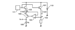
図11は従来の電流検出回路として、特許文献1に記載された電流検出回路を示す回路構成図である。図11において、出力トランジスタ101はNチャネルMOSFETで構成されており、ドレインが直流電源110に接続され、ソースが負荷103に接続される。負荷103の逆側は接地される。補助トランジスタ102はNチャネルMOSFETであり、ドレインが直流電源110に接続され、ソースが補償トランジスタ105のソースに接続される。出力トランジスタ101のソース電流I101と補助トランジスタ102のソース電流I102との比I101/I102は、ドレイン、ゲート、ソースの各電位を両スイッチ素子で等しくした場合、実質上一定(以下、n=I101/I102とする)になるように設計される。これは、例えば、電流検出回路を内蔵したモノリシック集積回路を製造する場合、出力トランジスタ101と補助トランジスタ102のゲート長を同じとし、ゲート幅をn:1にすれば実現できる。補償トランジスタ105はPチャネルMOSFETであり、ドレインが電流検出用抵抗106の一端に接続される。電流検出用抵抗106の他端は接地される。差動アンプ104は、補助トランジスタ102と補償トランジスタ105との接続点Qに対する出力トランジスタ101と負荷103との接続点Pの電位を検出する。差動アンプ104は、検出した電位差を増幅し、その増幅された電圧を補償トランジスタ105のゲートへ出力する。駆動回路111は、出力トランジスタ101及び補助トランジスタ102の各ゲートへ共通の駆動信号を出力する。
FIG. 11 is a circuit configuration diagram showing a current detection circuit described in
以下、図11に示した従来の電流検出回路の動作を説明する。
まず、差動アンプ104と補償トランジスタ105とにより、接続点Qに対する接続点Pの電位が正方向に増大すると接続点Qの電位が増大し、逆に負方向に増大すると接続点Qの電位が下降する。こうして、出力トランジスタ101のソース電位(接続点Pの電位)と補助トランジスタ102のソース電位(接続点Qの電位)とが実質的に等しくなる。また、出力トランジスタ101と補助トランジスタ102におけるそれぞれのドレイン電位及びゲート電位は回路構成から明らかなように等しい。従って、出力トランジスタ101と補助トランジスタ102の両トランジスタのドレイン、ゲート及びソースの各電位は等しく、出力トランジスタ101のソース電流I101と補助トランジスタ102のソース電流I102との比I101/I102は、一定値nに保たれる。即ち、補助トランジスタ102のソース電流I102は、 I102=I101/n となり、電流検出用抵抗106には出力トランジスタ101のソース電流I101に比例した検出電圧Vsが発生する。電流検出用抵抗106の抵抗値をRsとすると、検出電圧Vsは、 Vs=Rs・I101/n となる。
First, by the
上記のように構成された従来の電流検出回路を、スイッチング電源のスイッチ素子に流れる電流の検出に適用する場合、負荷にはインダクタや整流回路が接続される。整流回路に同期整流回路が用いられる降圧コンバータの場合、出力に発生したオーバーシュートを速やかに抑制するためなどに、出力から入力へ電力が回生するようスイッチ素子の電流を逆流させることがある。しかしながら、上記のように構成された従来の電流検出回路においては、出力トランジスタから負荷の方向へ流れる電流しか検出することができなかった。即ち、上記のように構成された従来の電流検出回路ではスイッチング電源のスイッチ素子に流れる逆流電流が検出できなかった。 When the conventional current detection circuit configured as described above is applied to detection of a current flowing through a switching element of a switching power supply, an inductor and a rectifier circuit are connected to the load. In the case of a step-down converter in which a synchronous rectifier circuit is used for the rectifier circuit, the current of the switch element may be caused to flow backward so that power is regenerated from the output to the input in order to quickly suppress overshoot generated at the output. However, in the conventional current detection circuit configured as described above, the current flowing in the direction of the output transistor motor or we load only could be detected. That is, the conventional current detection circuit configured as described above cannot detect the reverse current flowing through the switching element of the switching power supply.
本発明は、スイッチ素子に流れる逆流電流を検出できる電流検出回路を提供し、これを用いることにより過渡応答特性を改善したスイッチング電源を提供することを目的とする。 It is an object of the present invention to provide a current detection circuit capable of detecting a backflow current flowing through a switch element, and to provide a switching power supply with improved transient response characteristics by using the current detection circuit.
上記課題を解決するために、本発明の第1の観点の電流検出回路は、スイッチ素子の電流を検出する電流検出回路であって、
前記スイッチ素子と並設されて、少なくとも前記スイッチ素子がオン状態の時にはオン状態である補助スイッチ素子と、
オフセット電圧を発生するオフセット電圧源と、
前記スイッチ素子の出力電位に前記オフセット電圧を加えた電位と前記補助スイッチ素子の出力電位が等しくなるように前記補助スイッチ素子の出力電流を調整する補償回路と、
を具備し、
前記オフセット電圧源は、オフセット用抵抗素子と、前記オフセット用抵抗素子に電流を流す電流源回路と、を有し、
前記オフセット用抵抗素子は、前記スイッチ素子と同チャネルのFETである。このように構成された本発明に係る電流検出回路は、スイッチ素子に流れる逆流電流を精度高く検出することができる。
In order to solve the above problem, a current detection circuit according to a first aspect of the present invention is a current detection circuit that detects a current of a switch element, and
Wherein it is switching elements and arranged, and the auxiliary switching element is in the ON state when at least the switching element is turned on,
An offset voltage source for generating an offset voltage;
A compensation circuit for adjusting the output current of the auxiliary switch element so that the potential obtained by adding the offset voltage to the output potential of the switch element is equal to the output potential of the auxiliary switch element;
Equipped with,
The offset voltage source includes an offset resistance element, and a current source circuit for passing a current through the offset resistance element,
The offset resistance element is an FET having the same channel as the switch element . The current detection circuit according to the present invention configured as described above can accurately detect the backflow current flowing through the switch element.
また、本発明の第2の観点の電流検出回路は、前記第1の観点の構成において、前記スイッチ素子と前記補助スイッチ素子とを同チャネルのFETで構成してもよい。
Further, the current detection circuit of the second aspect of the present invention, in the configuration of the first aspect, and the switching element and the auxiliary switching device but it may also be constituted by a FET of the same channel.
また、本発明の第3の観点の電流検出回路は、前記第1の観点または第2の観点における前記補償回路を、前記スイッチ素子の出力電位に前記オフセット電圧を加えた電位と、前記補助スイッチ素子の出力電位が入力される差動アンプと、前記補助スイッチ素子の出力端子に接続され、前記差動アンプの出力によってインピーダンスが変化する可変インピーダンス素子と、を有するよう構成してもよい。
According to a third aspect of the present invention, there is provided a current detection circuit comprising: the compensation circuit according to the first aspect or the second aspect ; a potential obtained by adding the offset voltage to an output potential of the switch element; A differential amplifier to which the output potential of the element is input, and a variable impedance element that is connected to the output terminal of the auxiliary switch element and whose impedance changes according to the output of the differential amplifier may be included.
本発明の第4の観点のスイッチング電源は、スイッチ素子と、前記スイッチ素子に接続されるインダクタと、前記インダクタの出力を整流する整流回路と、前記整流回路を流れる電流を平滑する平滑手段と、前記スイッチ素子の電流を検出する電流検出回路と、前記電流検出回路からの電流検出信号と前記平滑手段から出力される出力電圧が入力されて、前記出力電圧を制御するために前記スイッチ素子をオンオフする制御回路と、を具備するスイッチング電源であって、
前記電流検出回路は、
前記スイッチ素子と並設されて、少なくとも前記スイッチ素子がオン状態の時にはオン状態である補助スイッチ素子と、
オフセット電圧を発生するオフセット電圧源と、
前記スイッチ素子の出力電位に前記オフセット電圧を加えた電位と前記補助スイッチ素子の出力電位とが等しくなるように前記補助スイッチ素子の出力電流を調整する補償回路と、を有し、
前記オフセット電圧源は、オフセット用抵抗素子と、前記オフセット用抵抗素子に電流を流す電流源回路と、を有し、
前記オフセット用抵抗素子は、前記スイッチ素子と同チャネルのFETである。このように構成された本発明に係るスイッチング電源は、スイッチ素子に流れる逆流電流を検出できる電流検出回路を用いることにより優れた過渡応答特性を有する。
また、本発明の第5の観点のスイッチング電源は、前記第4の観点の構成において、前記スイッチ素子と前記補助スイッチ素子とを同チャネルのFETで構成してもよい。
また、本発明の第6の観点のスイッチング電源は、前記第4の観点または第5の観点における前記補償回路を、前記スイッチ素子の出力電位に前記オフセット電圧を加えた電位と、前記補助スイッチ素子の出力電位が入力される差動アンプと、前記補助スイッチ素子の出力端子に接続され、前記差動アンプの出力によってインピーダンスが変化する可変インピーダンス素子と、を有するよう構成してもよい。
A switching power supply according to a fourth aspect of the present invention includes a switch element, an inductor connected to the switch element, a rectifier circuit that rectifies the output of the inductor, and smoothing means that smoothes a current flowing through the rectifier circuit, A current detection circuit for detecting a current of the switch element, a current detection signal from the current detection circuit, and an output voltage output from the smoothing means are input, and the switch element is turned on / off to control the output voltage A switching power supply comprising:
The current detection circuit includes:
Auxiliary switch element that is provided in parallel with the switch element and is in an on state when at least the switch element is in an on state;
An offset voltage source for generating an offset voltage;
Have a, a compensation circuit for adjusting the output current of the auxiliary switching element so that the output potential of said auxiliary switching device to said offset voltage added to the output potential of the switching element is equal,
The offset voltage source includes an offset resistance element, and a current source circuit for passing a current through the offset resistance element,
The offset resistance element is an FET having the same channel as the switch element . The switching power supply according to the present invention configured as described above has excellent transient response characteristics by using a current detection circuit that can detect a backflow current flowing through the switch element.
In the switching power supply according to the fifth aspect of the present invention, in the configuration according to the fourth aspect, the switch element and the auxiliary switch element may be composed of FETs of the same channel.
According to a sixth aspect of the present invention, there is provided a switching power supply comprising: the compensation circuit according to the fourth aspect or the fifth aspect; a potential obtained by adding the offset voltage to an output potential of the switch element; and the auxiliary switch element. A differential amplifier to which the output potential is input, and a variable impedance element that is connected to the output terminal of the auxiliary switch element and whose impedance changes according to the output of the differential amplifier.
本発明の第7の観点のスイッチング電源は、前記第6の観点における前記制御回路が、出力電圧を制御するための制御信号を生成し、前記電流検出回路からの電流検出信号が前記制御信号に追従するように、前記スイッチ素子をオンオフするよう構成してもよい。
本発明の第8の観点のスイッチング電源は、前記第7の観点における前記整流回路が、整流スイッチ素子を有し、前記制御回路を前記スイッチ素子と前記整流スイッチ素子を交互にオンオフするよう構成してもよい。
本発明の第9の観点のスイッチング電源は、前記第7の観点における前記制御回路を、前記出力電圧が目標値を含む所定の範囲内にある時に、前記制御信号の変化幅を制限するよう構成してもよい。
In the switching power supply according to the seventh aspect of the present invention , the control circuit according to the sixth aspect generates a control signal for controlling the output voltage, and the current detection signal from the current detection circuit is used as the control signal. You may comprise so that the said switch element may be turned on and off so that it may track.
Switching power supply of an eighth aspect of the present invention, the said rectifier circuit in the seventh aspect of the rectifying switch includes a device, said control circuit said structure to OFF switch element and the rectifying switching element alternately formed it may be.
A switching power supply according to a ninth aspect of the present invention is configured such that the control circuit according to the seventh aspect limits the change width of the control signal when the output voltage is within a predetermined range including a target value. it may be.
本発明の第10の観点のスイッチング電源は、前記第7の観点における前記制御回路を、前記出力電圧が所定値以上の時に前記オフセット電圧を正の所定の電圧に増加させ、前記出力電圧が所定値以下の時に前記オフセット電圧を負の所定の電圧へ減少させるよう構成してもよい。
また、本発明の第11の観点のスイッチング電源は、スイッチ素子と、前記スイッチ素子に接続されるインダクタと、前記インダクタの出力を整流する整流回路と、前記整流回路を流れる電流を平滑する平滑手段と、前記スイッチ素子の電流を検出する電流検出回路と、前記電流検出回路からの電流検出信号と前記平滑手段から出力される出力電圧が入力されて、前記出力電圧を制御するために前記スイッチ素子をオンオフする制御回路と、を具備するスイッチング電源であって、
前記電流検出回路は、
前記スイッチ素子と並設されて、少なくとも前記スイッチ素子がオン状態の時にはオン状態である補助スイッチ素子と、
オフセット電圧を発生するオフセット電圧源と、
前記スイッチ素子の出力電位に前記オフセット電圧を加えた電位と前記補助スイッチ素子の出力電位とが等しくなるように前記補助スイッチ素子の出力電流を調整する補償回路と、を有し、
前記制御回路は、出力電圧を制御するための制御信号を生成し、前記電流検出回路からの電流検出信号が前記制御信号に追従するように、前記スイッチ素子をオンオフするよう構成され、
前記制御回路は、前記出力電圧が所定値以上の時に前記オフセット電圧を正の所定の電圧に増加し、前記出力電圧が所定値以下の時に前記オフセット電圧を負の所定の電圧へ減少するよう構成されている。このように構成された本発明に係るスイッチング電源は、スイッチ素子に流れる逆流電流を検出できる電流検出回路を用いることにより優れた過渡応答特性を有する。
A switching power supply according to a tenth aspect of the present invention is configured such that the control circuit according to the seventh aspect increases the offset voltage to a positive predetermined voltage when the output voltage is equal to or higher than a predetermined value. The offset voltage may be reduced to a predetermined negative voltage when the value is less than or equal to the value.
A switching power supply according to an eleventh aspect of the present invention is a switching element, an inductor connected to the switching element, a rectifier circuit that rectifies the output of the inductor, and a smoothing means that smoothes the current flowing through the rectifier circuit. A current detection circuit for detecting a current of the switch element, a current detection signal from the current detection circuit, and an output voltage output from the smoothing means, and the switch element for controlling the output voltage. A switching power supply comprising a control circuit for turning on and off,
The current detection circuit includes:
Auxiliary switch element that is provided in parallel with the switch element and is in an on state when at least the switch element is in an on state;
An offset voltage source for generating an offset voltage;
A compensation circuit that adjusts the output current of the auxiliary switch element so that the potential obtained by adding the offset voltage to the output potential of the switch element is equal to the output potential of the auxiliary switch element;
The control circuit is configured to generate a control signal for controlling an output voltage, and to turn on and off the switch element so that a current detection signal from the current detection circuit follows the control signal,
The control circuit is configured to increase the offset voltage to a positive predetermined voltage when the output voltage is equal to or higher than a predetermined value, and to decrease the offset voltage to a negative predetermined voltage when the output voltage is equal to or lower than the predetermined value. Has been. The switching power supply according to the present invention configured as described above has excellent transient response characteristics by using a current detection circuit that can detect a backflow current flowing through the switch element.
本発明に係る電流検出回路によれば、簡易な構成でスイッチ素子に流れる逆流電流を検出することができる。
また、本発明に係る電流検出回路を電流モード制御方式のスイッチング電源のスイッチ素子に流れる電流の検出に適用することにより、出力から入力へ電力が回生するように流れるスイッチ素子の逆流電流を検出・制御することが可能となる。このことにより、出力電流の急減などによって出力電圧に発生したオーバーシュートを速やかに抑制することができる。
According to the current detection circuit of the present invention, it is possible to detect the backflow current flowing through the switch element with a simple configuration.
Further, by applying the current detection circuit according to the present invention to the detection of the current flowing through the switching element of the switching power supply of the current mode control system, the reverse current of the switching element that flows so that power is regenerated from the output to the input can be detected and It becomes possible to control. As a result, an overshoot generated in the output voltage due to a sudden decrease in the output current can be quickly suppressed.
さらに、本発明に係る電流検出回路を用いた電流モード制御方式のスイッチング電源において、通常動作時には動作電流の設定値の変化幅を必要最小限に制限し、出力条件の急変などの過渡時には動作電流の設定値に設けた変化幅の制限を緩和することにより、応答性を高速化するとともに通常動作への復帰がスムーズになるという優れた効果を奏する。
また、本発明に係る電流検出回路を用いた電流モード制御方式のスイッチング電源において、電流検出回路のオフセットレベルを可変とし、出力条件の急変などの過渡時にはオフセットレベルを大きくすることによって検出レベルをシフトし、応答性を高速化するとともに通常動作への復帰もスムーズにできるという優れた効果を奏する。
Furthermore, in the switching power supply of the current mode control system using the current detection circuit according to the present invention, the change width of the set value of the operating current is limited to a necessary minimum during normal operation, and the operating current is changed during a transient such as a sudden change in output conditions. By relaxing the restriction on the change width provided for the set value, it is possible to increase the response speed and to smoothly return to the normal operation.
Also, in the current mode control type switching power supply using the current detection circuit according to the present invention, the offset level of the current detection circuit is made variable, and the detection level is shifted by increasing the offset level during a transient such as a sudden change in output conditions. In addition, there is an excellent effect of speeding up the responsiveness and smoothly returning to normal operation.
以下に、本発明に係る電流検出回路及びそれを用いたスイッチング電源の好適な実施の形態について、添付の図面を参照しつつ説明する。 Hereinafter, preferred embodiments of a current detection circuit according to the present invention and a switching power supply using the current detection circuit will be described with reference to the accompanying drawings.
《第1の実施の形態》
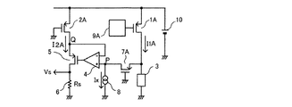
図1は、本発明に係る第1の実施の形態の電流検出回路の構成を示した回路図である。第1の実施の形態の電流検出回路において、出力トランジスタ1はスイッチ素子であり、NチャネルMISFET(Metal Insulator Semiconductor Field Effect:絶縁ゲート型電界効果トランジスタ)で構成されている。出力トランジスタに並設された補助トランジスタ2はNチャネルMISFETで構成されている。また、補償トランジスタ5はPチャネルMISFETで構成されている。図1において、3は負荷、4は差動アンプ、6は電流検出用抵抗、7はオフセット用抵抗、8は電流源回路、9は駆動回路、及び10は直流電源である。
<< First Embodiment >>
FIG. 1 is a circuit diagram showing a configuration of a current detection circuit according to a first embodiment of the present invention. In the current detection circuit of the first embodiment, the
出力トランジスタ1のドレインは直流電源10に接続され、ゲートは駆動回路9に接続され、そしてソースは負荷3に接続されている。補助トランジスタ2のドレインは直流電源10に接続され、ゲートは駆動回路9に接続され、ソースは補償トランジスタ5のソースに接続されている。負荷3の一端が出力トランジスタ1のソースに接続され、負荷3の他端が接地されており、オン状態の出力トランジスタ1のソースから電流が供給される。出力トランジスタ1のソース電流I1と補助トランジスタ2のソース電流I2との比I1/I2は、ドレイン、ゲート、ソースの各電位を両トランジスタで等しくした場合、実質上一定(以下、n=I1/I2とする)になるよう設計される。例えば、電流検出回路を内蔵したモノリシック集積回路を製造する場合、出力トランジスタ1と補助トランジスタ2のサイズの比をn:1とする。ここで、サイズの比をn:1とするとは、各トランジスタのゲート長を同じとし、ゲート幅をn:1にすることである。補償トランジスタ5のドレインは、電流検出用抵抗6の一方に接続される。電流検出用抵抗6の他方は接地されている。
The drain of the
出力トランジスタ1と負荷3との接続点にはオフセット用抵抗7の一端が接続され、オフセット用抵抗7の他端には電流源回路8が接続されている。電流源回路8の他端は接地されている。差動アンプ4の一方の入力端子は、補助トランジスタ2と補償トランジスタ5との接続点Qに接続されており、差動アンプ4の他方の入力端子は、オフセット用抵抗7と電流源回路8との接続点Pに接続されている。差動アンプ4は、接続点Qと接続点Pの電位差を検出し、その電位差を増幅した電圧を補償トランジスタ5のゲートへ出力する。
One end of an offset resistor 7 is connected to a connection point between the
駆動回路9は出力トランジスタ1と補助トランジスタ2に共通の駆動信号を出力し、出力トランジスタ1と補助トランジスタ2をオンオフする。第1の実施の形態において、駆動回路9の出力するHレベルの駆動信号は、出力トランジスタ1と補助トランジスタ2を充分オン状態とする高電位である。また、駆動回路9の出力するLレベルの駆動信号は、出力トランジスタ1と補助トランジスタ2を充分オフ状態とする低電位である。
The drive circuit 9 outputs a common drive signal to the
以下、図1に示した第1の実施の形態の電流検出回路の動作を説明する。
第1の実施の形態の電流検出回路において、差動アンプ4と補償トランジスタ5とにより、接続点Qに対する接続点Pの電位が正方向に増大すると、接続点Qの電位が増大する。逆に、接続点Qに対する接続点Pの電位が負方向に増大すると、接続点Qの電位が下降する。こうして、オフセット用抵抗7と電流源回路8との接続点Pの電位と補助トランジスタ2のソース電位(接続点Qの電位)とが実質的に等しくなる。
The operation of the current detection circuit according to the first embodiment shown in FIG. 1 will be described below.
In the current detection circuit according to the first embodiment, when the potential of the connection point P with respect to the connection point Q increases in the positive direction by the differential amplifier 4 and the
一方、駆動回路9によってオン状態にある出力トランジスタ1と補助トランジスタ2のオン抵抗は、前述のサイズの比(n:1)に実質的に反比例する。すなわち、出力トランジスタ1のオン抵抗をRonとすると、補助トランジスタ2のオン抵抗は、n・Ronとなる。従って、直流電源10の電位をVi、出力トランジスタ1のソース電流をI1とすると、出力トランジスタ1のソース電位は、(Vi−I1・Ron)となる。接続点Pの電位は、出力トランジスタ1のソース電位からオフセット用抵抗7の電圧降下分を引いたものであるから、オフセット用抵抗7の抵抗値をRx、電流源回路8の電流値をIxとすると、(Vi−I1・Ron−Ix・Rx)となる。接続点Qの電位は、補助トランジスタ2のソース電流をI2とすると、(Vi−n・Ron・I2)となる。この接続点Qの電位が接続点Pの電位と等しくなることより、補助トランジスタ2のソース電流I2は次式で表される。
On the other hand, the on-resistance of the
I2=(I1+Ix・Rx/Ron)/n (1) I2 = (I1 + Ix · Rx / Ron) / n (1)
電流検出用抵抗6には、電流検出用抵抗6の抵抗値をRsとすると、出力トランジスタ1のソース電流I1と次式(2)の関係にある検出電圧Vsが発生する。
When the resistance value of the current detection resistor 6 is Rs, the current detection resistor 6 generates a detection voltage Vs having the relationship of the following equation (2) with the source current I1 of the
Vs=Rs・(I1+Ix・Rx/Ron)/n (2) Vs = Rs · (I1 + Ix · Rx / Ron) / n (2)
図2は、第1の実施の形態の電流検出回路の特性図を表わしており、上式(2)の関係を図示したものである。電流源回路8の電流値Ixがゼロ(Ix=0)であれば、(2)式は、 Vs=Rs・I1/n となり、検出電圧Vsは出力トランジスタ1のソース電流I1に比例する。この場合、ソース電流I1は正方向のみの検出が可能である。
FIG. 2 is a characteristic diagram of the current detection circuit according to the first embodiment, and illustrates the relationship of the above equation (2). If the current value Ix of the
電流源回路8の電流値Ixがゼロより大きい場合(Ix>0)、検出電圧Vsは出力トランジスタ1のソース電流I1がゼロであっても、電圧(Rs・Ix・Rx/Ron/n)を示し、さらにソース電流I1が負になっても、Vs=0となる値(−Ix・Rx/Ron)までの範囲で検出可能である。
電流源回路8の電流値Ixがゼロより小さい場合(Ix<0)、即ち、電流源回路8の電流がオフセット用抵抗7を逆方向に流れる場合には、Vs=0となる(−Ix・Rx/Ron)の値も正値を示す。この場合には、より大きな出力トランジスタ1のソース電流I1が検出可能となる。
When the current value Ix of the
When the current value Ix of the
以上のように、本発明に係る第1の実施の形態の電流検出回路においては、オフセット用抵抗7と電流源回路8とを設けて、検出電流にオフセットをかけることにより、出力トランジスタ1のソース電流I1が負方向に流れても検出することが可能となる。
尚、第1の実施の形態の電流検出回路において、オフセット用抵抗7及び電流源回路8によりオフセット電圧源が構成されている。また、差動アンプ4及び補償トランジスタ5により補償回路が構成されている。
As described above, in the current detection circuit according to the first embodiment of the present invention, the source of the
In the current detection circuit of the first embodiment, the offset resistor 7 and the
《第2の実施の形態》
以下、本発明に係る第2の実施の形態の電流検出回路を添付の図3を用いて説明する。図3は第2の実施の形態の電流検出回路の構成を示した回路図である。
図3において、1Aはスイッチ素子であり、PチャネルMISFETである出力トランジスタ、2AはPチャネルMISFETである補助トランジスタ、3は負荷、4は差動アンプ、5はPチャネルMISFETである補償トランジスタ、6は電流検出用抵抗、7AはPチャネルMISFETであるオフセット用抵抗素子、8は電流源回路、9Aは駆動回路、10は直流電源である。第2の実施の形態の電流検出回路において、前述の図1に示した第1の実施の形態の電流検出回路の構成と異なるところは、出力トランジスタ1Aと補助トランジスタ2Aとオフセット用抵抗素子7AがPチャネルMISFETで構成されている点と、補助トランジスタ2Aのゲートとオフセット用抵抗素子7Aのゲートが接地されている点である。他の構成は図1に示した第1の実施の形態と同様であるので、その詳細な説明は省略する。
<< Second Embodiment >>
Hereinafter, a current detection circuit according to a second embodiment of the present invention will be described with reference to FIG. FIG. 3 is a circuit diagram showing a configuration of the current detection circuit according to the second embodiment.
In FIG. 3, 1A is a switching element, an output transistor that is a P-channel MISFET, 2A is an auxiliary transistor that is a P-channel MISFET, 3 is a load, 4 is a differential amplifier, 5 is a compensation transistor that is a P-channel MISFET, 6 Is a current detection resistor, 7A is an offset resistance element which is a P-channel MISFET, 8 is a current source circuit, 9A is a drive circuit, and 10 is a DC power supply. The current detection circuit of the second embodiment differs from the configuration of the current detection circuit of the first embodiment shown in FIG. 1 in that the
図3において、出力トランジスタ1Aのソースは直流電源10に接続され、ゲートは駆動回路9Aに接続され、ドレインは負荷3に接続されている。補助トランジスタ2Aのソースは直流電源10に接続され、ゲートは接地され、ドレインは補償トランジスタ5のソースに接続される。オフセット用抵抗素子7Aは、ソースが出力トランジスタ1Aと負荷3との接続点に接続され、ドレインが電流源回路8に接続され、ゲートが接地されている。
In FIG. 3, the source of the
第2の実施の形態の電流検出回路は、モノリシック集積回路に内蔵されており、出力トランジスタ1Aと補助トランジスタ2Aとオフセット用抵抗素子7Aのサイズの比をn:1:kとする。ここで、サイズの比をn:1:kとするとは、各トランジスタのゲート長を同じとし、ゲート幅をn:1:kにすることである。
The current detection circuit of the second embodiment, Ri Contact incorporated in the monolithic integrated circuit, the size ratio of the
差動アンプ4は、補助トランジスタ2Aと補償トランジスタ5の接続点Qに対するオフセット用抵抗素子7Aと電流源回路8との接続点Pの電位を検出し、その電位差を増幅する。そして、差動アンプ4は、増幅した電圧を補償トランジスタ5のゲートへ出力する。駆動回路9Aは出力トランジスタ1Aに駆動信号を出力し、出力トランジスタ1Aをオンオフする。ここで、駆動回路9Aが出力するLレベルの駆動信号は、出力トランジスタ1Aを充分オン状態とする接地電位である。また、駆動回路9Aが出力するHレベルの駆動信号は、出力トランジスタ1Aを充分オフ状態とする高電位(例えば電源電圧Vi)である。
The differential amplifier 4 detects the potential at the connection point P between the offset
以下、図3に示した第2の実施の形態の電流検出回路における動作について説明する。
第2の実施の形態の電流検出回路において、差動アンプ4と補償トランジスタ5とにより、前述の第1の実施の形態と同様に、接続点Qに対する接続点Pの電位が正方向に増大すると、接続点Qの電位が増大する。逆に、接続点Qに対する接続点Pの電位が負方向に増大すると、接続点Qの電位が下降する。こうして、オフセット用抵抗素子7Aと電流源回路8との接続点Pの電位と補助トランジスタ2Aのドレイン電位(接続点Qの電位)とが実質的に等しくなる。
The operation in the current detection circuit of the second embodiment shown in FIG. 3 will be described below.
In the current detection circuit of the second embodiment, when the potential at the connection point P with respect to the connection point Q increases in the positive direction by the differential amplifier 4 and the
補助トランジスタ2Aはゲートが接地されているので常にオン状態である。駆動回路9Aによってオン状態にある出力トランジスタ1Aと補助トランジスタ2Aのオン抵抗は、前述の各トランジスタのサイズの比(n:1:k)に実質的に反比例する。すなわち、出力トランジスタ1Aのオン抵抗をRonとすると、補助トランジスタ2Aのオン抵抗は、n・Ron となる。また、オフセット用抵抗素子7Aもゲートを接地されてオン状態にあり、その抵抗値は、(n/k)・Ron となる。従って、直流電源10の電位をVi、出力トランジスタ1Aのドレイン電流をI1Aとすると、出力トランジスタ1Aのドレイン電位は、(Vi−I1A・Ron)となる。接続点Pの電位は、出力トランジスタ1Aのドレイン電位からオフセット用抵抗素子7Aの電圧降下分を引いたものであるから、電流源回路8の電流値をIxとすると、(Vi−I1A・Ron−Ix・(n/k)・Ron)となる。接続点Qの電位は、補助トランジスタ2Aのドレイン電流をI2Aとすると、(Vi−n・Ron・I2A)となる。接続点Qの電位が接続点Pの電位と等しくなることより、補助トランジスタ2Aのドレイン電流I2Aは次式で表される。
The
I2A=I1A/n+Ix/k (3) I2A = I1A / n + Ix / k (3)
電流検出用抵抗6には、電流検出用抵抗6の抵抗値をRsとすると、出力トランジスタ1Aのドレイン電流I1Aと次式(4)の関係にある検出電圧Vsが発生する。
When the resistance value of the current detection resistor 6 is Rs, the current detection resistor 6 generates a detection voltage Vs having a relationship of the following equation (4) with the drain current I1A of the
Vs=Rs・(I1A/n+Ix/k) (4) Vs = Rs · (I1A / n + Ix / k) (4)
以上のように、本発明に係る第2の実施の形態の電流検出回路においては、オフセット用抵抗素子7Aと電流源回路8により検出電流にオフセットをかけることにより、出力トランジスタ1Aのドレイン電流I1Aが負方向に流れても検出することができる。また、オフセット用抵抗素子7Aを、オン状態においてサイズの比に応じたオン抵抗となるように、出力トランジスタ1Aと同様のPチャネルMISFETとすることにより、オン抵抗における温度特性や製造バラツキの影響を検出電圧Vsから除去することができる。このため、本発明に係る第2の実施の形態の電流検出回路においては、精度の高い電流検出が可能となる。
As described above, in the current detection circuit according to the second embodiment of the present invention, the drain current I1A of the
《第3の実施の形態》
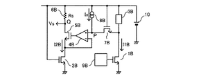
以下、本発明に係る第3の実施の形態の電流検出回路を添付の図4を用いて説明する。図4は第3の実施の形態の電流検出回路の構成を示した回路図である。
図4に示すように、第3の実施の形態の電流検出回路においては、負荷3Bが電源電位側に接続され、スイッチ素子である出力トランジスタ1Bがソースを接地したNチャネルMISFETで構成されている。図4において、補助トランジスタ2B、補償トランジスタ5B、及びオフセット用抵抗素子7Bは、全てNチャネルMISFETで構成されている。補助トランジスタ2Bとオフセット用抵抗素子7Bの各ゲートは電源電位Viとなっており、補助トランジスタ2Bのソースは接地されている。電流源回路8Bはオフセット用抵抗素子7Bへ電流を流し込むよう構成されており、電流検出用抵抗6Bは電源電位側に接続されている。
<< Third Embodiment >>
Hereinafter, a current detection circuit according to a third embodiment of the present invention will be described with reference to FIG. FIG. 4 is a circuit diagram showing a configuration of a current detection circuit according to the third embodiment.
As shown in FIG. 4, in the current detection circuit of the third embodiment, the
以上のように、第3の実施の形態の電流検出回路は、前述の図3に示した第2の実施の形態の電流検出回路における電源電位側と接地電位側への接続を逆転させた構成である。従って、第3の実施の形態の電流検出回路は、電流の向きと電圧の正負が反転しているだけで第2の実施の形態の電流検出回路と等価である。 As described above, the current detection circuit according to the third embodiment has a configuration in which the connection between the power supply potential side and the ground potential side in the current detection circuit according to the second embodiment shown in FIG. 3 is reversed. It is. Therefore, the current detection circuit according to the third embodiment is equivalent to the current detection circuit according to the second embodiment only in that the direction of the current and the sign of the voltage are reversed.
《第4の実施の形態》
本発明に係る第4の実施の形態のスイッチング電源を添付の図5及び図6用いて説明する。図5は第4の実施の形態のスイッチング電源の構成を示した回路図であり、図6は第4の実施の形態のスイッチング電源における要部動作波形図である。第4の実施の形態のスイッチング電源は、前述の第2の実施の形態の電流検出回路の構成を有するスイッチング電源である。
<< Fourth Embodiment >>
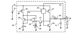
A switching power supply according to a fourth embodiment of the present invention will be described with reference to FIGS. FIG. 5 is a circuit diagram showing a configuration of the switching power supply according to the fourth embodiment, and FIG. 6 is an operation waveform diagram of main parts of the switching power supply according to the fourth embodiment. The switching power supply according to the fourth embodiment is a switching power supply having the configuration of the current detection circuit according to the second embodiment described above.
図5において、第4の実施の形態のスイッチング電源は、電源電圧Viを出力する直流電源10と降圧コンバータ20とを具備しており、負荷32に対して出力電流Ioを供給する。降圧コンバータ20は、PチャネルMISFETからなるスイッチ素子21と、PチャネルMISFETからなる補助トランジスタ22と、NチャネルMISFETからなる同期整流トランジスタ23と、差動アンプ24と、PチャネルMISFETからなる補償トランジスタ25と、抵抗値Rsを有する電流検出用抵抗26と、PチャネルMISFETからなるオフセット用抵抗素子27と、電流源回路28と、スイッチ素子21と同期整流トランジスタ23を駆動する制御回路29と、インダクタ30と、出力コンデンサ31とを有する。ここで、同期整流トランジスタ23が整流回路であり、出力コンデンサ31が平滑手段である。
In FIG. 5, the switching power supply according to the fourth embodiment includes a
第4の実施の形態のスイッチング電源において、少なくともスイッチ素子21と補助トランジスタ22とオフセット用抵抗素子27は、モノリシック集積回路に内蔵されており、スイッチ素子21と補助トランジスタ22とオフセット用抵抗素子27のサイズの比をn:1:kとする。尚、第4の実施の形態のスイッチング電源におけるスイッチ素子21が前述の第2の実施の形態の電流検出回路における出力トランジスタ1Aに相当する。
制御回路29は、電流検出用抵抗26から検出電圧Vsが入力され、出力コンデンサ31から負荷32に供給される出力電圧Voを検出する。そして、制御回路29は、出力電圧Voを安定化させるように、検出電圧Vsの上限値を設定し、スイッチ素子21と同期整流トランジスタ23を交互にオンオフする。
In the switching power supply of the fourth embodiment, at least the
The
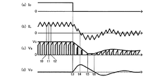
図6において、(a)は出力コンデンサ31から負荷32に供給される出力電流Io、(b)はインダクタ30に流れる電流IL、(c)は検出電圧Vsと制御回路29によって設定される検出電圧Vsの上限設定値Vc、及び(d)は出力電圧Voの変動を示す波形である。
6A shows an output current Io supplied from the
以下、図6の要部動作波形図を参照しながら、第4の実施の形態のスイッチング電源の動作について説明する。
まず、図6の波形図における左側部分(時刻t3まで状態)の通常動作について説明する。
時刻t0において、制御回路29からの駆動信号によって、同期整流トランジスタ23がオフ状態になり、スイッチ素子21がオン状態になると、直流電源10からスイッチ素子21を介してインダクタ30に電流が流れる。このインダクタ電流ILは、インダクタ30への印加電圧である降圧コンバータ20の入出力電圧差(Vi−Vo)に比例して時間と共に増加していく。補助トランジスタ22と差動アンプ24と補償トランジスタ25と電流検出用抵抗26とオフセット用抵抗素子27と電流源回路28は第2の実施の形態で示した電流検出回路と同様の構成であり、電流検出用抵抗26には次式(5)で表される検出電圧Vsが発生する。
The operation of the switching power supply according to the fourth embodiment will be described below with reference to the main part operation waveform diagram of FIG.
First, the normal operation of the left portion (state until time t3) in the waveform diagram of FIG. 6 will be described.
At time t0, when the
Vs=Rs・(IL/n+Ix/k) (5) Vs = Rs · (IL / n + Ix / k) (5)
制御回路29は出力電圧Voを検出し、出力電圧Voを安定化するように検出電圧の上限設定値Vcを設定し、検出電圧Vsを上限設定値Vcと比較する。時刻t1において、検出電圧Vsが上限設定値Vcに達すると、制御回路29はスイッチ素子21をオフ状態とし、続いて同期整流トランジスタ23をオン状態とする。インダクタ電流ILは、インダクタ30への印加電圧である出力電圧Voに比例して時間と共に減少していく。制御回路29は内部に発振器(図示なし)を有し、時刻t2において、同期整流トランジスタ23をオフ状態とし、スイッチ素子21をオン状態とする。制御回路29は以上の動作を繰り返す。検出電圧Vsの上限設定値Vcが高くなると、スイッチ素子21のオン状態が長くなってインダクタ電流ILのピーク値が大きくなり、出力コンデンサ31を充電する電流が増える。逆に上限設定値Vcが低くなると、インダクタ電流ILのピーク値が小さくなり、出力コンデンサ31を充電する電流が減る。即ち、上限設定値Vcの設定により出力電力を制御することができる。このようにインダクタ電流ILを制御することにより出力電圧Voを安定化する制御方法を電流モード制御方式という。
The
次に、図6の時刻t3において、出力電流Ioが急減してゼロになった場合の動作を説明する。
出力電流Ioが急減した後、降圧コンバータ20は負荷32への電力供給が過剰となり、出力電圧Voは上昇する。制御回路29は上昇した出力電圧Voを元に戻すために、検出電圧Vsの上限設定値Vcを下げる。上限設定値Vcの低下に従い、スイッチ素子21のオン時間は短くなり、インダクタ電流ILは減少する。時刻t4において、インダクタ電流ILはゼロになるが、検出電圧Vsは Rs・Ix/k である。出力電圧Voの上昇はこの時点で停止する。時刻t4以降のインダクタ電流ILはゼロを下回り、やがて時刻t5において、インダクタ電流ILのピーク値が Vc=0 に相当する −(n/k)・Ix まで減少して出力電圧Voが下がり続ける。時刻t6において、出力電圧Voが目標値に近づくと、制御回路29は上限設定値Vcを上昇させ、出力電圧Voの低下を制動する。この後、出力電圧Voは減衰振動しながら目標値に達する。
Next, the operation when the output current Io suddenly decreases to zero at time t3 in FIG. 6 will be described.
After the output current Io rapidly decreases, the step-
以上のように、本発明に係る第4の実施の形態のスイッチング電源は、負方向の電流も制御可能な電流モード制御方式であるので、負荷急減などによる出力電圧の上昇に対し、インダクタ電流を逆流させることにより、上昇した出力電圧を急速に低下させている。このため、第4の実施の形態のスイッチング電源によれば、出力電圧のオーバーシュートの発生を抑制し、且つ目標値への復帰が速いという優れた効果を得ることができる。
尚、第4の実施の形態のスイッチング電源において、オフセット用抵抗素子27及び電流源回路28によりオフセット電圧源が構成されている。また、差動アンプ24及び補償トランジスタ25により補償回路が構成されている。
As described above, since the switching power supply according to the fourth embodiment of the present invention is a current mode control method that can also control a negative current, an inductor current is controlled against an increase in output voltage due to a sudden decrease in load or the like. By making it reverse flow, the output voltage which rose is rapidly reduced. For this reason, according to the switching power supply of 4th Embodiment, generation | occurrence | production of the overshoot of output voltage can be suppressed and the outstanding effect that the return to a target value is quick can be acquired.
In the switching power supply according to the fourth embodiment, the offset
《第5の実施の形態》
以下、本発明に係る第5の実施の形態のスイッチング電源を添付の図7及び図8用いて説明する。図7は第5の実施の形態のスイッチング電源の構成を示した回路図である。図8は第5の実施の形態のスイッチング電源におけるインダクタ電流ILと検出電圧Vsの関係を示す特性図である。図7において、図5に示した第4の実施の形態のスイッチング電源と同じ機能、構成を有する要素には同じ番号を付与し、その説明は省略する。第5の実施の形態のスイッチング電源において、第4の実施の形態の構成と異なるところは制御回路の構成であり、第4の実施の形態における制御回路29に出力電圧の急変に対応できる機能が追加されている。従って、第5の実施の形態においては、図5に示した第4の実施の形態の制御回路29と区別するため、制御回路29Aとし、その内部構成を以下具体的に説明する。
<< Fifth Embodiment >>
A switching power supply according to a fifth embodiment of the present invention will be described below with reference to FIGS. FIG. 7 is a circuit diagram showing the configuration of the switching power supply according to the fifth embodiment. FIG. 8 is a characteristic diagram showing the relationship between the inductor current IL and the detection voltage Vs in the switching power supply according to the fifth embodiment. In FIG. 7, elements having the same functions and configurations as those of the switching power supply according to the fourth embodiment shown in FIG. The switching power supply of the fifth embodiment is different from the configuration of the fourth embodiment in the configuration of the control circuit, and the
図7において、制御回路29Aは、基準電圧源290と出力電圧検出回路291と誤差アンプ292と第1の比較器293と第2の比較器294と第1のクランプ回路295と第2のクランプ回路296とクロック回路297と電流比較器298とRSラッチ299と駆動回路300とを有する。基準電圧源290は可変であり、誤差アンプ292の正入力端子と第1の比較器293の負入力端子と第2の比較器294の正入力端子に基準電圧Vrを印加する。出力電圧検出回路291は抵抗2911〜2914の直列回路からなり、出力電圧Voを分圧する。抵抗2911と抵抗2912の接続点は第1の比較器293の正入力端子に接続され、抵抗2912と抵抗2913の接続点は誤差アンプ292の負入力端子に接続され、抵抗2913と抵抗2914の接続点は第2の比較器294の負入力端子に接続される。
In FIG. 7, the
誤差アンプ292の出力は上限設定値Vcであり、電流比較器298の負入力端子に接続される。第1の比較器293の出力は第1のクランプ回路295に入力される。第1のクランプ回路295は、第1の比較器293の出力がHレベルの時、上限設定値Vcを第1の設定電圧Vc1以下にクランプし、第1の比較器293の出力がLレベルの時、上限設定値Vcに対する第1の設定電圧Vc1以下とするクランプを解除する。第2の比較器294の出力は第2のクランプ回路296に入力される。第2のクランプ回路296は、第2の比較器294の出力がHレベルの時、上限設定値Vcを第2の設定電圧Vc2以上にクランプし、第2の比較器294の出力がLレベルの時、上限設定値Vcに対する第2の設定電圧Vc2以上とするクランプを解除する。
The output of the
クロック回路297は、所定の周波数のクロック信号をRSラッチ299のセット端子へ出力する。電流比較器298は、正入力端子に電流検出信号である検出電圧Vsが入力され、負入力端子に上限設定値Vcが入力され、RSラッチ299のリセット端子へ出力する。駆動回路300は、RSラッチ299の出力に基づいて、スイッチ素子21と同期整流トランジスタ23を交互にオンオフする。
The
次に、第5の実施の形態のスイッチング電源における制御回路29Aの動作を説明する。
まず、通常時の動作を説明する。出力電圧Voは出力電圧検出回路291によって分圧され、誤差アンプ292において基準電圧Vrと比較される。このとき、基準電圧Vrは第1の電圧Vr1に設定されている。誤差アンプ292の出力である検出電圧の上限設定値Vcは、出力電圧Voが目標値よりも高いと低下し、出力電圧Voが目標値よりも低いと上昇する。クロック回路297からのクロック信号によりセットされたRSラッチ299はHレベルを出力し、駆動回路300によって同期整流トランジスタ23がオフ状態とされ、スイッチ素子21がオン状態とされる。この結果、直流電源10よりスイッチ素子21を介してインダクタ30に電流が流れる。このインダクタ電流ILの増加とともに検出電圧Vsも上昇する。
Next, the operation of the
First, the normal operation will be described. The output voltage Vo is divided by the output
検出電圧Vsが上限設定値Vcを上回ると電流比較器298の出力がHレベルとなり、リセットされたRSラッチ299はLレベルの信号を出力する。RSラッチ299からのLレベルの信号により、駆動回路300はスイッチ素子21をオフ状態とし、同期整流トランジスタ23をオン状態とする。この状態はクロック回路297からのクロック信号が発生するまでである。クロック回路297からのクロック信号がRSラッチ299に入力されると、RSラッチ299はHレベルを出力し、前述の動作を繰り返す。このように、スイッチ素子21と同期整流トランジスタ23は駆動回路300により交互にオンオフされて、降圧コンバータ20は安定した出力電圧Voを負荷32へ供給する。この通常時の動作においては、出力電圧Voは目標値に安定化されているため、第1の比較器293及び第2の比較器294はいずれもHレベルを出力し、上限設定値Vcは第2の設定電圧Vc2以上であり、且つ第1の設定電圧Vc1以下にクランプされている。
When the detection voltage Vs exceeds the upper limit set value Vc, the output of the
次に、出力電圧Voを別の目標値に急速に上昇させるために、基準電圧源290の基準電圧Vrを第1の電圧Vr1から第2の電圧Vr2へと急に高くした場合の動作について説明する。
基準電圧Vrが第1の電圧Vr1から第2の電圧Vr2へと変化したため、誤差アンプ292は出力電圧Voを上昇させるために、上限設定値Vcを上昇させる。同時に、第1の比較器293は負入力端子への印加電圧が第2の電圧Vr2に上昇したので、出力がLレベルとなり、上限設定値Vcに対する第1の設定電圧Vc1以下とするクランプを解除する。このため、上限設定値Vcは第1の設定電圧Vc1より高くなり、インダクタ電流ILも通常動作での最大値より大きくなって、出力コンデンサ31への充電が急速に進む。そして、出力電圧Voが基準電圧源290の第2の電圧Vr2で設定される目標値に近づくと、第1の比較器293は出力がHレベルとなり、上限設定値Vcに対する第1の設定電圧Vc1以下になるようクランプがかかる。このため、上限設定値Vcは第1の設定電圧Vc1まで低下し、インダクタ電流ILは通常動作時の最大値に制限され、出力コンデンサ31への充電動作に制動が加わる。やがて上限設定値Vcは第1の設定電圧Vc1より下降し、出力電圧Voは基準電圧源290の第2の電圧Vr2により設定された目標値に安定化される。
Next, an operation when the reference voltage Vr of the
Since the reference voltage Vr has changed from the first voltage Vr1 to the second voltage Vr2, the
次に、出力電圧Voをさらに別の目標値に急速に低下させるために、基準電圧源290の基準電圧Vrを第2の電圧Vr2から第1の電圧Vr1へと急に低くした場合の動作を説明する。
基準電圧Vrが第2の電圧Vr2から第1の電圧Vr1へと変化したため、誤差アンプ292は出力電圧Voを低下させるために、上限設定値Vcを低下させる。同時に、第2の比較器294は正入力端子への印加電圧が第1の電圧Vr1に低下したので、出力がLレベルとなり、上限設定値Vcに対する第2の設定電圧Vc2以上とするクランプを解除する。このため、上限設定値Vcは第2の設定電圧Vc2より低くなり、インダクタ電流ILも通常動作での最小値より小さくなって逆流し、出力コンデンサ31からの放電が急速に進む。そして、出力電圧Voが第1の電圧Vr1で設定される目標値に近づくと、第2の比較器294は出力がHレベルとなり、上限設定値Vcに対する第2の設定電圧Vc2以上となるクランプがかかる。このため、上限設定値Vcは第2の設定電圧Vc2まで上昇し、インダクタ電流ILは通常動作時の最小値に制限され、出力コンデンサ31からの放電動作に制動が加わる。やがて上限設定値Vcは第2の設定電圧Vc2より上昇し、出力電圧Voは第1の電圧Vr1で設定される目標値に安定化される。
Next, the operation when the reference voltage Vr of the
Since the reference voltage Vr has changed from the second voltage Vr2 to the first voltage Vr1, the
図8は第5の実施の形態のスイッチング電源におけるインダクタ電流ILと検出電圧Vsの関係を示す特性図である。
図8に示すように、第5の実施の形態のスイッチング電源において、インダクタ電流ILはその変化幅が通常動作時では第1の設定電圧Vc1と第2の設定電圧Vc2とで設定された範囲内に制限されており必要最小限に抑制されている。そして、必要な期間においては、インダクタ電流ILの制限範囲を外して、電力の供給と回生を急速に行っている。従って、第5の実施の形態のスイッチング電源は、出力電圧の急変などに高速に対応し、且つ通常動作への復帰もスムーズに行うことができる。
FIG. 8 is a characteristic diagram showing the relationship between the inductor current IL and the detection voltage Vs in the switching power supply according to the fifth embodiment.
As shown in FIG. 8, in the switching power supply according to the fifth embodiment, the change width of the inductor current IL is within a range set by the first set voltage Vc1 and the second set voltage Vc2 during normal operation. It is limited to the necessary minimum. In a necessary period, the limit range of the inductor current IL is removed, and power is supplied and regenerated rapidly. Therefore, the switching power supply according to the fifth embodiment can cope with a sudden change in output voltage at high speed and can smoothly return to normal operation.
《第6の実施の形態》
以下、本発明に係る第6の実施の形態のスイッチング電源を添付の図9及び図10用いて説明する。図9は第6の実施の形態のスイッチング電源の構成を示した回路図である。図10は第6の実施の形態のスイッチング電源におけるインダクタ電流ILと検出電圧Vsの関係を示す特性図である。
図9において、図5に示した第4の実施の形態のスイッチング電源と同じ機能、構成を有する要素には同じ番号を付与し、その説明は省略する。第6の実施の形態のスイッチング電源において、第4の実施の形態の構成と異なるところは電流源回路と制御回路の構成である。従って、第6の実施の形態においては、図5に示した第4の実施の形態の電流源回路28及び制御回路29と区別するため、電流源回路28B及び制御回路29Bとし、その内部構成を以下具体的に説明する。
<< Sixth Embodiment >>
Hereinafter, a switching power supply according to a sixth embodiment of the present invention will be described with reference to FIGS. FIG. 9 is a circuit diagram showing a configuration of a switching power supply according to the sixth embodiment. FIG. 10 is a characteristic diagram showing the relationship between the inductor current IL and the detection voltage Vs in the switching power supply according to the sixth embodiment.
In FIG. 9, elements having the same functions and configurations as those of the switching power supply according to the fourth embodiment shown in FIG. The switching power supply of the sixth embodiment is different from the configuration of the fourth embodiment in the configuration of the current source circuit and the control circuit. Therefore, in the sixth embodiment, the
以下、図9に示した第6の実施の形態のスイッチング電源における電流源回路28Bと制御回路29Bの構成について説明する。
図9において、電流源回路28Bは、オフセット用抵抗素子27のドレインからの電流を接地へ流す出す第1の電流源回路281と、オフセット用抵抗素子27のドレインに電流を流し込む第2の電流源回路282とを有している。第1の電流源回路281と第2の電流源回路282はそれぞれ制御端子を有しており、それらの制御端子にHレベルの信号が入力されると、第1の電流源回路281と第2の電流源回路282が活性化される構成である。
The configurations of the
In FIG. 9, the
図9に示すスイッチング電源における制御回路29Bにおいて、図7に示した第5の実施の形態における制御回路29Aと同じ機能、構成を有するものには同じ番号を付与し、その説明は省略する。図9の制御回路29Bにおいて、図7の制御回路29Aの構成と異なるのは、第1の比較器293と第2の比較器294の代わりに第1の比較器293Bと第2の比較器294Bとを用い、第1のクランプ回路295と第2のクランプ回路296が設けられていない点である。
In the
制御回路29Bでは、第1の比較器293Bの正入力端子と第2の比較器294Bの負入力端子に基準電圧源290の基準電圧Vrが印加されている。また、抵抗2911と抵抗2912の接続点は第1の比較器293Bの負入力端子に接続され、抵抗2913と抵抗2914の接続点は第2の比較器294Bの正入力端子に接続される。第1の比較器293Bの出力V3は第1の電流源回路281の制御端子に印加され、第2の比較器294Bの出力V4は、第2の電流源回路282の制御端子に印加される。
In the
次に、第6の実施の形態のスイッチング電源の動作について説明する。
まず、通常時の動作を説明する。出力電圧Voは出力電圧検出回路291によって分圧され、誤差アンプ292によって基準電圧源290の基準電圧Vrと比較される。誤差アンプ292の出力である検出電圧の上限設定値Vcは、出力電圧Voが目標値よりも高いと低下し、出力電圧Voが目標値よりも低いと上昇する。クロック回路297からのクロック信号でセットされたRSラッチ299はHレベルを出力し、駆動回路300によって同期整流トランジスタ23がオフ状態とされ、スイッチ素子21がオン状態とされる。この状態において、直流電源10よりスイッチ素子21を介してインダクタ30に電流が流れる。このインダクタ電流ILの増加とともに検出電圧Vsも上昇する。検出電圧Vsが上限設定値Vcを上回ると電流比較器298の出力がHレベルとなり、リセットされたRSラッチ299はLレベルの信号を出力する。このLレベルの信号により、駆動回路300はスイッチ素子21をオフ状態とし、同期整流トランジスタ23をオン状態とする。この状態はクロック回路297からのクロック信号が発生するまでである。
Next, the operation of the switching power supply according to the sixth embodiment will be described.
First, the normal operation will be described. The output voltage Vo is divided by the output
クロック回路297からのクロック信号がRSラッチ299に入力されると、RSラッチ299はHレベルを出力し、前述の動作を繰り返す。このように、スイッチ素子21と同期整流トランジスタ23は駆動回路300により交互にオンオフされて、降圧コンバータ20は安定した出力電圧Voを負荷32へ供給する。この通常時の動作においては、出力電圧Voは目標値に安定化されているため、第1の比較器293B及び第2の比較器294BはいずれもLレベルを出力し、電流源回路28Bの第1の電流源回路281と第2の電流源回路282はいずれも不活性である。このため、オフセット用抵抗素子27には電流が流れず、その両端電圧はゼロである。即ち、オフセット電圧は発生せず、電流検出用抵抗26に発生する検出電圧Vsは、スイッチ素子21に流れる電流に比例する。
When the clock signal from the
次に、出力電圧Voを別の目標値に急速に上昇させるために、基準電圧Vrが第1の電圧Vr1から第2の電圧Vr2へ急に高くした場合の動作を説明する。
基準電圧Vrが第1の電圧Vr1から第2の電圧Vr2へと変化したため、誤差アンプ292は出力電圧Voを上昇させるために、上限設定値Vcが上昇する。同時に、第1の比較器293Bは正入力端子への印加電圧が第2の電圧Vr2に上昇したので、出力V3がHレベルとなり、電流源回路28Bの第1の電流源回路281を活性化する。このため、第1の電流源回路281の電流によってオフセット用抵抗素子27には電圧が発生し、電流検出用抵抗26に発生する検出電圧Vsは、スイッチ素子21に流れる電流に比例する電圧から所定値だけ低下した電圧となる。即ち、上限設定値Vcは元のままであるが、検出電圧Vsが低くなるために、検出電圧Vsが上限設定値Vcに追従するように、スイッチ素子21のオン時間は長くなる。結果的にインダクタ電流ILは通常動作での最大値より大きくなり、出力コンデンサ31への充電が急速に進む。そして、出力電圧Voが基準電圧源290の第2の電圧Vr2で設定された目標値に近づくと、第1の比較器293Bは出力V3がLレベルとなり、第1の電流源回路281は不活性化されて電流を流さなくなる。このため、オフセット用抵抗素子27にはオフセット電圧は発生せず、電流検出用抵抗26に発生する検出電圧Vsは、スイッチ素子21に流れる電流に比例する電圧に戻り、検出電圧Vsが高くなる。結果的にインダクタ電流ILは通常動作時の最大値に制限され、出力コンデンサ31への充電に制動が加わった状態となる。やがて上限設定値Vcは下降し、出力電圧Voは基準電圧源290の第2の電圧Vr2で設定された目標値に安定化される。
Next, an operation when the reference voltage Vr is suddenly increased from the first voltage Vr1 to the second voltage Vr2 in order to rapidly increase the output voltage Vo to another target value will be described.
Since the reference voltage Vr has changed from the first voltage Vr1 to the second voltage Vr2, the
次に、出力電圧Voをさらに別の目標値に急速に低下させるために、基準電圧Vrが第2の電圧Vr2から第1の電圧Vr1へ急に低くした場合の動作を説明する。
基準電圧Vrが第2の電圧Vr2から第1の電圧Vr1へと変化したため、誤差アンプ292は出力電圧Voを低下させるために、上限設定値Vcが低下する。同時に、第2の比較器294Bは負入力端子への印加電圧が第1の電圧Vr1に低下したため、出力V4がHレベルとなり、電流源回路28Bの第2の電流源回路282を活性化する。このため、第2の電流源回路282の電流によってオフセット用抵抗素子27には電圧が発生し、電流検出用抵抗26に発生する検出電圧Vsは、スイッチ素子21に流れる電流に比例する電圧から所定値だけ上昇した電圧となる。即ち、上限設定値Vcは元のままであるが、検出電圧Vsが高くなるために、検出電圧Vsが上限設定値Vcに追従するように、スイッチ素子21のオン時間は短くなる。結果的にインダクタ電流ILも通常動作での最小値より小さくなって逆流し、出力コンデンサ31からの放電が急速に進む。そして、出力電圧Voが基準電圧源290の第1の電圧Vr1で設定された目標値に近づくと、第2の比較器294Bは出力V4がLレベルとなり、第2の電流源回路282は不活性化されて電流を流さなくなる。このため、オフセット用抵抗素子27にはオフセット電圧は発生せず、電流検出用抵抗26に発生する検出電圧Vsは、スイッチ素子21に流れる電流に比例する電圧に戻り、検出電圧Vsが低くなる。結果的にインダクタ電流ILは通常動作時の最小値に制限され、出力コンデンサ31からの放電に制動が加わった状態となる。やがて上限設定値Vcは上昇し、出力電圧Voは基準電圧源290の第1の電圧Vr1で設定された目標値に安定化される。
Next, an operation when the reference voltage Vr is suddenly lowered from the second voltage Vr2 to the first voltage Vr1 in order to rapidly reduce the output voltage Vo to another target value will be described.
Since the reference voltage Vr has changed from the second voltage Vr2 to the first voltage Vr1, the
図10は、第6の実施の形態のスイッチング電源におけるインダクタ電流ILと検出電圧Vsの関係を示す特性図である。通常動作時には第1の比較器293Bの出力V3と第2の比較器294Bの出力V4はともにLレベルであり、電流源回路28Bの第1の電流源回路281と第2の電流源回路282はいずれも不活性である。このため、オフセット電圧は発生せず、電流検出用抵抗26に発生する検出電圧Vsは、スイッチ素子21に流れる電流に比例する。そして、出力電圧Voを変更するために、第1の比較器293Bの出力V3もしくは第2の比較器294Bの出力V4がHレベルとなると、スイッチング電源における電流検出回路のオフセット電圧を発生させている。
図10に示すように、第6の実施の形態のスイッチング電源においては、インダクタ電流ILに対する検出電圧Vsの関係をインダクタ電流ILの零値を挟んで前後にシフトさせることにより、電力の供給と回生を急速に行うことができる。この結果、第6の実施の形態のスイッチング電源は、出力電圧の急変などに高速に対応することができ、且つ通常動作への復帰もスムーズに行うことができる。
FIG. 10 is a characteristic diagram showing the relationship between the inductor current IL and the detection voltage Vs in the switching power supply according to the sixth embodiment. During normal operation, the output V3 of the
As shown in FIG. 10, in the switching power supply according to the sixth embodiment, the relationship between the detection voltage Vs and the inductor current IL is shifted back and forth across the zero value of the inductor current IL, thereby supplying and regenerating power. Can be done rapidly. As a result, the switching power supply according to the sixth embodiment can cope with a rapid change in the output voltage at a high speed and can smoothly return to the normal operation.
尚、前述の第4の実施の形態から第6の実施の形態において、スイッチング電源として降圧コンバータを用いて説明してきたが、本発明に係る電流検出回路は降圧コンバータへの適用のみならず、ほとんど全てのスイッチング電源に適用可能である。例えば、第1の実施の形態や第2の実施の形態のように電源電位側に接続されるスイッチ素子の電流検出回路であれば、降圧コンバータや反転コンバータ、ブリッジコンバータのハイサイドスイッチの電流を検出することができる。また、第3の実施の形態のように接地電位側に接続されるスイッチ素子の電流検出回路であれば、昇圧コンバータや1石式絶縁コンバータ、ブリッジコンバータのローサイドスイッチの電流を検出することができる。 In the fourth to sixth embodiments described above, the step-down converter is used as the switching power supply. However, the current detection circuit according to the present invention is not only applied to the step-down converter, Applicable to all switching power supplies. For example, if the current detection circuit of the switch element is connected to the power supply potential side as in the first embodiment or the second embodiment, the current of the high-side switch of the step-down converter, the inverting converter, or the bridge converter is calculated. Can be detected. In addition, if the current detection circuit of the switch element is connected to the ground potential side as in the third embodiment, the current of the low-side switch of the boost converter, the one-stone insulation converter, or the bridge converter can be detected. .
上記のように、本発明に係る電流検出回路は、いずれの形式のコンバータに適用しても、第4の実施の形態から第6の実施の形態において説明したスイッチング電源の優れた効果を奏するものである。
尚、上記の各実施の形態において、スイッチ素子としてMISFETで構成した例で説明したが、このMISFETはMOSFETを含む電界効果トランジスタであり、MISFETとしてMOSFETを使用しても同様の効果を奏する。
As described above, the current detection circuit according to the present invention exhibits the excellent effects of the switching power supply described in the fourth to sixth embodiments regardless of which type of converter is applied. It is.
In each of the above-described embodiments, an example in which the MISFET is used as the switching element has been described. However, the MISFET is a field effect transistor including a MOSFET, and the same effect can be obtained even if the MOSFET is used as the MISFET .
本発明に係る電流検出回路は、MISFETのようなトランジスタにおいて負方向に流れる電流を検出することができ、この電流検出回路を用いたスイッチング電源は、出力条件の急変に対し高速に応答して出力電圧を安定化させることができる電源として有用である。 The current detection circuit according to the present invention can detect a current flowing in the negative direction in a transistor such as a MISFET, and the switching power supply using this current detection circuit outputs in response to a sudden change in output conditions at a high speed. It is useful as a power source that can stabilize the voltage.
1 出力トランジスタ
2 補助トランジスタ
3 負荷
4 差動アンプ
5 補償トランジスタ
6 電流検出用抵抗
7 オフセット用抵抗
8 電流源回路
9 駆動回路
10 直流電源
21 スイッチ素子
22 補助トランジスタ
23 同期整流トランジスタ
24 差動アンプ
25 補償トランジスタ
26 電流検出用抵抗
27 オフセット用抵抗素子
28 電流源回路
29 制御回路
30 インダクタ
31 出力コンデンサ
32 負荷
DESCRIPTION OF
Claims (11)
前記スイッチ素子と並設されて、少なくとも前記スイッチ素子がオン状態の時にはオン状態である補助スイッチ素子と、
オフセット電圧を発生するオフセット電圧源と、
前記スイッチ素子の出力電位に前記オフセット電圧を加えた電位と前記補助スイッチ素子の出力電位が等しくなるように前記補助スイッチ素子の出力電流を調整する補償回路と、
を具備し、
前記オフセット電圧源は、オフセット用抵抗素子と、前記オフセット用抵抗素子に電流を流す電流源回路と、を有し、
前記オフセット用抵抗素子は、前記スイッチ素子と同チャネルのFETである電流検出回路。 A current detection circuit for detecting a current of a switch element,
Auxiliary switch element that is provided in parallel with the switch element and is in an on state when at least the switch element is in an on state;
An offset voltage source for generating an offset voltage;
A compensation circuit for adjusting the output current of the auxiliary switch element so that the potential obtained by adding the offset voltage to the output potential of the switch element is equal to the output potential of the auxiliary switch element;
Equipped with,
The offset voltage source includes an offset resistance element, and a current source circuit for passing a current through the offset resistance element,
The current detecting circuit , wherein the offset resistance element is a FET having the same channel as the switch element .
前記スイッチ素子の出力電位に前記オフセット電圧を加えた電位と、前記補助スイッチ素子の出力電位が入力される差動アンプと、
前記補助スイッチ素子の出力端子に接続され、前記差動アンプの出力によってインピーダンスが変化する可変インピーダンス素子と、を有する請求項1または2に記載の電流検出回路。 The compensation circuit includes:
A potential obtained by adding the offset voltage to the output potential of the switch element; and a differential amplifier to which the output potential of the auxiliary switch element is input;
The auxiliary switch is connected to the output terminal of the device, a current detecting circuit according to claim 1 or 2 having a variable impedance element impedance is changed by the output of said differential amplifier.
前記電流検出回路は、
前記スイッチ素子と並設されて、少なくとも前記スイッチ素子がオン状態の時にはオン状態である補助スイッチ素子と、
オフセット電圧を発生するオフセット電圧源と、
前記スイッチ素子の出力電位に前記オフセット電圧を加えた電位と前記補助スイッチ素子の出力電位とが等しくなるように前記補助スイッチ素子の出力電流を調整する補償回路と、を有し、
前記オフセット電圧源は、オフセット用抵抗素子と、前記オフセット用抵抗素子に電流を流す電流源回路と、を有し、
前記オフセット用抵抗素子は、前記スイッチ素子と同チャネルのFETであるスイッチング電源。 A switch element; an inductor connected to the switch element; a rectifier circuit that rectifies the output of the inductor; smoothing means that smoothes a current flowing through the rectifier circuit; and a current detection circuit that detects a current of the switch element; A switching power supply comprising: a current detection signal from the current detection circuit and an output voltage output from the smoothing means; and a control circuit for turning on and off the switch element to control the output voltage. And
The current detection circuit includes:
Auxiliary switch element that is provided in parallel with the switch element and is in an on state when at least the switch element is in an on state;
An offset voltage source for generating an offset voltage;
Have a, a compensation circuit for adjusting the output current of the auxiliary switching element so that the output potential of said auxiliary switching device to said offset voltage added to the output potential of the switching element is equal,
The offset voltage source includes an offset resistance element, and a current source circuit for passing a current through the offset resistance element,
The offset resistance element is a switching power supply which is a FET of the same channel as the switch element .
前記スイッチ素子の出力電位に前記オフセット電圧を加えた電位と、前記補助スイッチ素子の出力電位が入力される差動アンプと、A potential obtained by adding the offset voltage to the output potential of the switch element; and a differential amplifier to which the output potential of the auxiliary switch element is input;
前記補助スイッチ素子の出力端子に接続され、前記差動アンプの出力によってインピーダンスが変化する可変インピーダンス素子と、を有する請求項4または5に記載のスイッチング電源。The switching power supply according to claim 4, further comprising: a variable impedance element that is connected to an output terminal of the auxiliary switch element and has an impedance that varies depending on an output of the differential amplifier.
前記電流検出回路は、The current detection circuit includes:
前記スイッチ素子と並設されて、少なくとも前記スイッチ素子がオン状態の時にはオン状態である補助スイッチ素子と、Auxiliary switch element that is provided in parallel with the switch element and is in an on state when at least the switch element is in an on state;
オフセット電圧を発生するオフセット電圧源と、An offset voltage source for generating an offset voltage;
前記スイッチ素子の出力電位に前記オフセット電圧を加えた電位と前記補助スイッチ素子の出力電位とが等しくなるように前記補助スイッチ素子の出力電流を調整する補償回路と、を有し、A compensation circuit that adjusts the output current of the auxiliary switch element so that the potential obtained by adding the offset voltage to the output potential of the switch element is equal to the output potential of the auxiliary switch element;
前記制御回路は、出力電圧を制御するための制御信号を生成し、前記電流検出回路からの電流検出信号が前記制御信号に追従するように、前記スイッチ素子をオンオフするよう構成され、The control circuit is configured to generate a control signal for controlling an output voltage, and to turn on and off the switch element so that a current detection signal from the current detection circuit follows the control signal,
前記制御回路は、前記出力電圧が所定値以上の時に前記オフセット電圧を正の所定の電圧に増加し、前記出力電圧が所定値以下の時に前記オフセット電圧を負の所定の電圧へ減少するよう構成されたスイッチング電源。The control circuit is configured to increase the offset voltage to a positive predetermined voltage when the output voltage is equal to or higher than a predetermined value, and to decrease the offset voltage to a negative predetermined voltage when the output voltage is equal to or lower than the predetermined value. Switching power supply.
Priority Applications (3)
| Application Number | Priority Date | Filing Date | Title |
|---|---|---|---|
| JP2004226094A JP4097635B2 (en) | 2004-08-02 | 2004-08-02 | Current detection circuit and switching power supply using the same |
| US11/195,835 US7323850B2 (en) | 2004-08-02 | 2005-08-02 | Current detection circuit and switching power supply using the same |
| US11/843,896 US7479771B2 (en) | 2004-08-02 | 2007-08-23 | Current detection circuit and switching power supply |
Applications Claiming Priority (1)
| Application Number | Priority Date | Filing Date | Title |
|---|---|---|---|
| JP2004226094A JP4097635B2 (en) | 2004-08-02 | 2004-08-02 | Current detection circuit and switching power supply using the same |
Publications (2)
| Publication Number | Publication Date |
|---|---|
| JP2006050724A JP2006050724A (en) | 2006-02-16 |
| JP4097635B2 true JP4097635B2 (en) | 2008-06-11 |
Family
ID=35756775
Family Applications (1)
| Application Number | Title | Priority Date | Filing Date |
|---|---|---|---|
| JP2004226094A Active JP4097635B2 (en) | 2004-08-02 | 2004-08-02 | Current detection circuit and switching power supply using the same |
Country Status (2)
| Country | Link |
|---|---|
| US (2) | US7323850B2 (en) |
| JP (1) | JP4097635B2 (en) |
Families Citing this family (36)
| Publication number | Priority date | Publication date | Assignee | Title |
|---|---|---|---|---|
| TWI249090B (en) * | 2003-01-16 | 2006-02-11 | Shindengen Electric Mfg | Switching circuit |
| JP3916163B2 (en) * | 2004-02-19 | 2007-05-16 | ローム株式会社 | Current direction detection circuit and switching regulator provided with the same |
| JP4980588B2 (en) * | 2005-06-21 | 2012-07-18 | ローム株式会社 | Step-down switching regulator, its control circuit, and electronic equipment using the same |
| JP4842614B2 (en) * | 2005-10-27 | 2011-12-21 | ルネサスエレクトロニクス株式会社 | Current detection circuit |
| JP5055517B2 (en) * | 2006-02-17 | 2012-10-24 | 日本電産サンキョー株式会社 | Pump system |
| US7336085B2 (en) * | 2006-02-17 | 2008-02-26 | Infineon Technologies Ag | Current sensing circuit |
| US20080266911A1 (en) * | 2007-04-30 | 2008-10-30 | O2Micro Inc | Current sensing circuits and methods for a converter |
| JP2008295158A (en) * | 2007-05-23 | 2008-12-04 | Panasonic Corp | Power supply device |
| JP5217319B2 (en) | 2007-09-12 | 2013-06-19 | 株式会社リコー | Constant current output control type switching regulator |
| US8004866B2 (en) * | 2008-01-03 | 2011-08-23 | Teknic, Inc. | Method and apparatus to remove energy from DC loads |
| JP4702403B2 (en) * | 2008-06-06 | 2011-06-15 | ミツミ電機株式会社 | Semiconductor integrated circuit for charge control |
| KR100925394B1 (en) * | 2008-09-25 | 2009-11-09 | 주식회사 하이닉스반도체 | Semiconductor Memory Apparatus |
| EP2356737B1 (en) * | 2008-12-09 | 2018-02-28 | Hewlett-Packard Enterprise Development LP | Power circuit |
| JP5135199B2 (en) * | 2008-12-22 | 2013-01-30 | パナソニック株式会社 | Current detection circuit and voltage converter using the same |
| US8232781B2 (en) * | 2008-12-23 | 2012-07-31 | Stmicroelectronics S.R.L. | Device for measuring the current flowing through a power transistor of a voltage regulator |
| US7911260B2 (en) * | 2009-02-02 | 2011-03-22 | Infineon Technologies Ag | Current control circuits |
| DE102009001899B4 (en) | 2009-03-26 | 2024-01-18 | Robert Bosch Gmbh | Measuring a load current of a breaker |
| EP2239591B1 (en) | 2009-04-08 | 2012-05-30 | Alcatel Lucent | Use of a current monitor in a control device for controlling a switching stage of an envelope tracking modulator |
| JP5586211B2 (en) * | 2009-11-17 | 2014-09-10 | 株式会社東芝 | DC-DC converter and semiconductor integrated circuit |
| JP2011220767A (en) * | 2010-04-07 | 2011-11-04 | Panasonic Corp | Current detection circuit |
| US9490636B2 (en) * | 2010-12-08 | 2016-11-08 | Panasonic Intellectual Property Management Co., Ltd. | Power supply circuit, power supply method and power supply system |
| EP2515126A1 (en) | 2011-04-19 | 2012-10-24 | Dialog Semiconductor GmbH | Bidirectional current sense |
| US10041982B2 (en) | 2012-08-15 | 2018-08-07 | Texas Instruments Incorporated | Switch mode power converter current sensing apparatus and method |
| JP2014226026A (en) * | 2013-04-15 | 2014-12-04 | ローム株式会社 | Dc/dc converter and electronic apparatus using the same |
| US20140361790A1 (en) * | 2013-06-11 | 2014-12-11 | Advantest Corporation | Drive circuit, switch apparatus, and test apparatus |
| US10128749B2 (en) * | 2014-05-12 | 2018-11-13 | Texas Instruments Incorporated | Method and circuitry for sensing and controlling a current |
| US10156592B2 (en) * | 2015-12-30 | 2018-12-18 | Nxp Usa, Inc. | Current sensing circuit and method |
| US9742398B2 (en) * | 2016-01-13 | 2017-08-22 | Texas Instruments Incorporated | Methods and apparatus for sensing current through power semiconductor devices with reduced sensitivity to temperature and process variations |
| JP7008478B2 (en) * | 2017-11-15 | 2022-01-25 | 新日本無線株式会社 | Current sense amplifier circuit and switching power supply |
| JP7079158B2 (en) * | 2018-06-27 | 2022-06-01 | エイブリック株式会社 | Voltage regulator |
| CN109254188B (en) * | 2018-10-09 | 2023-12-01 | 成都铱通科技有限公司 | High-speed current detection circuit suitable for switching power supply |
| KR102052947B1 (en) * | 2019-04-17 | 2020-01-22 | 시스트로닉스 주식회사 | Apparatus for controlling heating mat based on IoT and signal processing method thereof |
| JP2022045499A (en) | 2020-09-09 | 2022-03-22 | ミツミ電機株式会社 | Electric current detection circuit and switch circuit |
| JP7434129B2 (en) * | 2020-09-24 | 2024-02-20 | 株式会社東芝 | Current detection circuit, current detection system, and power supply circuit |
| CN113534884B (en) * | 2021-08-10 | 2022-08-12 | 江苏应能微电子有限公司 | Circuit for sampling current of MOSFET power tube with low power consumption |
| CN115833560B (en) * | 2022-11-24 | 2023-07-25 | 华南理工大学 | SenseFET type full-wave inductance current sensor |
Family Cites Families (14)
| Publication number | Priority date | Publication date | Assignee | Title |
|---|---|---|---|---|
| US3577019A (en) * | 1968-09-24 | 1971-05-04 | Gen Electric | Insulated gate field effect transistor used as a voltage-controlled linear resistor |
| JPH04134271A (en) | 1990-09-27 | 1992-05-08 | Nec Corp | Output circuit |
| JP2000166279A (en) | 1998-12-01 | 2000-06-16 | Mitsubishi Electric Corp | Current detection circuit |
| JP2000092824A (en) | 1998-09-10 | 2000-03-31 | Matsushita Electric Ind Co Ltd | Switching regulator and lsi system |
| CN1159846C (en) | 1999-06-18 | 2004-07-28 | 松下电器产业株式会社 | Output controller |
| US6166528A (en) | 1999-11-02 | 2000-12-26 | Fairchild Semiconductor Corporation | Lossless current sensing in buck converters working with low duty cycles and high clock frequencies |
| JP2002281743A (en) | 2001-03-19 | 2002-09-27 | Hitachi Ltd | Semiconductor integrated circuit and portable electronic apparatus |
| AU2003220665A1 (en) * | 2002-04-03 | 2003-10-20 | International Rectifier Corporation | Synchronous buck converter improvements |
| US6850401B2 (en) | 2002-05-28 | 2005-02-01 | Matsushita Electric Industrial Co., Ltd. | DC-DC converter |
| JP4360833B2 (en) | 2002-05-28 | 2009-11-11 | パナソニック株式会社 | DC-DC converter |
| US6798177B1 (en) * | 2002-10-15 | 2004-09-28 | Arques Technology, Inc. | Boost-buck cascade converter for pulsating loads |
| US7102415B1 (en) * | 2004-03-26 | 2006-09-05 | National Semiconductor Corporation | Trip-point detection circuit |
| US7268526B1 (en) * | 2004-04-21 | 2007-09-11 | National Semiconductor Corporation | Switch mode power supply control circuit |
| US7327149B2 (en) * | 2005-05-10 | 2008-02-05 | Power-One, Inc. | Bi-directional MOS current sense circuit |
-
2004
- 2004-08-02 JP JP2004226094A patent/JP4097635B2/en active Active
-
2005
- 2005-08-02 US US11/195,835 patent/US7323850B2/en active Active
-
2007
- 2007-08-23 US US11/843,896 patent/US7479771B2/en active Active
Also Published As
| Publication number | Publication date |
|---|---|
| JP2006050724A (en) | 2006-02-16 |
| US7479771B2 (en) | 2009-01-20 |
| US20060028192A1 (en) | 2006-02-09 |
| US20080018387A1 (en) | 2008-01-24 |
| US7323850B2 (en) | 2008-01-29 |
Similar Documents
| Publication | Publication Date | Title |
|---|---|---|
| JP4097635B2 (en) | Current detection circuit and switching power supply using the same | |
| US7403365B2 (en) | Over-current detection circuit and method for power-supply device | |
| US7436162B2 (en) | Buck converter having improved transient response to load step down | |
| US7868599B2 (en) | Method of optimum current blanking time implementation in current sense circuit | |
| US7138786B2 (en) | Power supply driver circuit | |
| US8193793B2 (en) | DC-DC converter | |
| KR101037306B1 (en) | Switching?regulator and?method?of?adjusting pulse?width?formed?in?same | |
| US7683593B2 (en) | Current sensing in a power converter | |
| JP6039327B2 (en) | Switching power supply | |
| JP4717449B2 (en) | Switching regulator circuit | |
| JP4854451B2 (en) | Boost converter | |
| TW200843306A (en) | Current detector circuit and current mode switching regulator | |
| JP2010136510A (en) | Step-down switching regulator | |
| JP2005086931A (en) | Switching power supply and semiconductor integrated circuit used for it | |
| JP2009207242A (en) | Power supply device | |
| JP2007053892A (en) | Dc-dc converter | |
| WO2018037898A1 (en) | Semiconductor device | |
| CN106558979B (en) | Semiconductor device with a plurality of semiconductor chips | |
| JP6588634B2 (en) | Switching regulator, semiconductor integrated circuit, and electronic device | |
| US10020733B2 (en) | Adaptive controller for a voltage converter | |
| JP2006238603A (en) | Switching regulator | |
| JP2007501598A (en) | Synchronous rectifier output voltage control | |
| WO2021054027A1 (en) | Power supply device | |
| WO2022254995A1 (en) | Amplification circuit, switching power supply circuit, and switching power supply device | |
| US20230387805A1 (en) | Switching power supply circuit and switching power supply device |
Legal Events
| Date | Code | Title | Description |
|---|---|---|---|
| A977 | Report on retrieval |
Free format text: JAPANESE INTERMEDIATE CODE: A971007 Effective date: 20070202 |
|
| A131 | Notification of reasons for refusal |
Free format text: JAPANESE INTERMEDIATE CODE: A131 Effective date: 20070814 |
|
| A521 | Request for written amendment filed |
Free format text: JAPANESE INTERMEDIATE CODE: A523 Effective date: 20071015 |
|
| RD03 | Notification of appointment of power of attorney |
Free format text: JAPANESE INTERMEDIATE CODE: A7423 Effective date: 20071015 |
|
| TRDD | Decision of grant or rejection written | ||
| A01 | Written decision to grant a patent or to grant a registration (utility model) |
Free format text: JAPANESE INTERMEDIATE CODE: A01 Effective date: 20080212 |
|
| A61 | First payment of annual fees (during grant procedure) |
Free format text: JAPANESE INTERMEDIATE CODE: A61 Effective date: 20080311 |
|
| R150 | Certificate of patent or registration of utility model |
Ref document number: 4097635 Country of ref document: JP Free format text: JAPANESE INTERMEDIATE CODE: R150 Free format text: JAPANESE INTERMEDIATE CODE: R150 |
|
| FPAY | Renewal fee payment (event date is renewal date of database) |
Free format text: PAYMENT UNTIL: 20110321 Year of fee payment: 3 |
|
| FPAY | Renewal fee payment (event date is renewal date of database) |
Free format text: PAYMENT UNTIL: 20110321 Year of fee payment: 3 |
|
| FPAY | Renewal fee payment (event date is renewal date of database) |
Free format text: PAYMENT UNTIL: 20120321 Year of fee payment: 4 |
|
| FPAY | Renewal fee payment (event date is renewal date of database) |
Free format text: PAYMENT UNTIL: 20130321 Year of fee payment: 5 |
|
| FPAY | Renewal fee payment (event date is renewal date of database) |
Free format text: PAYMENT UNTIL: 20130321 Year of fee payment: 5 |
|
| FPAY | Renewal fee payment (event date is renewal date of database) |
Free format text: PAYMENT UNTIL: 20140321 Year of fee payment: 6 |
|
| S533 | Written request for registration of change of name |
Free format text: JAPANESE INTERMEDIATE CODE: R313533 |
|
| R350 | Written notification of registration of transfer |
Free format text: JAPANESE INTERMEDIATE CODE: R350 |
|
| S111 | Request for change of ownership or part of ownership |
Free format text: JAPANESE INTERMEDIATE CODE: R313113 |
|
| R350 | Written notification of registration of transfer |
Free format text: JAPANESE INTERMEDIATE CODE: R350 |
|
| R250 | Receipt of annual fees |
Free format text: JAPANESE INTERMEDIATE CODE: R250 |
|
| R250 | Receipt of annual fees |
Free format text: JAPANESE INTERMEDIATE CODE: R250 |
|
| R250 | Receipt of annual fees |
Free format text: JAPANESE INTERMEDIATE CODE: R250 |
|
| R250 | Receipt of annual fees |
Free format text: JAPANESE INTERMEDIATE CODE: R250 |