JP4054598B2 - Memory control circuit, DMA request block, and memory access system - Google Patents
Memory control circuit, DMA request block, and memory access system Download PDFInfo
- Publication number
- JP4054598B2 JP4054598B2 JP2002123811A JP2002123811A JP4054598B2 JP 4054598 B2 JP4054598 B2 JP 4054598B2 JP 2002123811 A JP2002123811 A JP 2002123811A JP 2002123811 A JP2002123811 A JP 2002123811A JP 4054598 B2 JP4054598 B2 JP 4054598B2
- Authority
- JP
- Japan
- Prior art keywords
- dma
- burst
- dma request
- signal
- memory
- Prior art date
- Legal status (The legal status is an assumption and is not a legal conclusion. Google has not performed a legal analysis and makes no representation as to the accuracy of the status listed.)
- Expired - Fee Related
Links
Images


Classifications
-
- G—PHYSICS
- G06—COMPUTING; CALCULATING OR COUNTING
- G06F—ELECTRIC DIGITAL DATA PROCESSING
- G06F13/00—Interconnection of, or transfer of information or other signals between, memories, input/output devices or central processing units
- G06F13/14—Handling requests for interconnection or transfer
- G06F13/20—Handling requests for interconnection or transfer for access to input/output bus
- G06F13/28—Handling requests for interconnection or transfer for access to input/output bus using burst mode transfer, e.g. direct memory access DMA, cycle steal
Description
【0001】
【発明の属する技術分野】
本発明は、SDRAMを使用したメモリ制御回路に関するものである。
【0002】
【従来の技術】
SDRAMは非同期DRAMを高速に動作させるために考案された、比較的新しいデバイスである。
【0003】
その制御方法は、従来の非同期DRAMと似ているが、同期用にCLK信号を使用する、SDRAMへのアクセスはコマンドによって行う、連続してデータのリード/ライトが実行可能(バーストモード)である、等の点が特徴的である。
【0004】
図4は、標準的なSDRAMへのアクセスを示すタイミングチャートである。ここではバースト長(BL)=2の場合を示す。
【0005】
SDRAMへの実際のアクセス方法において、SDRAMコントローラは、まず、ACTVコマンドの発行と同時にRASアドレスを出力し、次にWRITEAまたはREADAコマンドの発行と同時にCASアドレスを出力する。(以下の説明においては、特にことわりのない限り、ACTVコマンド後1CLKで次のコマンドを受け付け可能とする。)
このときWRITAであれば、同時にデータバスラインにライトすべきデータを出力し、ライト動作を行う。READAである場合は、固有のディレイ値(CAS LATENCY=CL)分遅れた後、SDRAMよりリードデータが出力されるので、これを取り込む。
【0006】
ところで、上記のWRITA/READAを利用する場合は、バースト回数が、BURST LENGTH(=BL)で指定される値で一定であるため、任意のバースト回数を実行しようとした場合、MRSコマンドを発行してBL値を変更し、組み合わせで所望のバースト回数に到達するように制御する必要があり、トータルのスループットは低下してしまう。そこで、上記WRITA/READAコマンドを使用せず、SDRAMコントローラが所望のバースト回数に到達した場合に、バースト動作を中断させる方法もある。
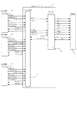
図5は、一般的なDMAコントローラの構成の一例を示したブロック図である。一般に、DMA要求ブロックはアプリケーションによって構成が異なり、一方、メモリコントローラ部はメモリの種類によって回路が異なるため、様々なアプリケーションやメモリへの対応を容易にするため、アービトレーション部とメモリコントローラ部とは独立した構成をとった方が良い。
【0007】
この場合、各DMA要求ブロック1−1・・・1−Nからアービタ回路3へは、DMA要求信号DREQ_1・・N、及びアドレス信号ADDRESS_1・・・N、リード/ライトのどちらの要求であるかを示すDR−WX_1・・・N、バースト回数を表すBSTNUM_1・・・N、ライトデータ用バスWRDATA_1・・・N等の信号が出力される。
【0008】
これに対して、アービタ回路3から各DMA要求ブロック1−1・・・1−Nには、負論理のDMA要求受諾信号であるREQACKX_1・・・N、リードデータ用バスのRDDATA_1・・・N、負論理のメモリアクセス信号であるDTACKX_1・・・N信号が出力される。
【0009】
尚、本説明では、全てのDMA要求ブロック1−1・・・1−NにWRDATA及びRDDATAが接続されているが、実際には各DMA要求ブロックは、リードまたはライトのどちらか一方しか行わない場合があり、その場合、使用しないデータバスは接続しなくてもよい。また、この図ではSDRAMのリフレッシュを制御する回路を省略している。
【0010】
一方、アービタ回路3からSDRAMコントローラ4へは、調停後のDMA要求信号REQ、及び調停後のアドレス信号ADRS、調停後のリード/ライト識別信号R−WX、バースト回数を表すBSTNUM、ライトデータ用バスWRDATA等の信号が出力される。逆にSDRAMコントローラ4からアービタ回路3には、リードデータ用バスのRDDATA、負論理のメモリアクセス信号であるORG_DTACKXが出力される。上記のような構成をとり、アービタ回路3とメモリコントローラ部4との間のインターフェースを統一することにより、さまざまなアプリケーションやメモリへの対応が容易になる。
【0011】
図6は、このような制御を行う場合のDMAコントローラ全体の動きを示すタイミングチャートである。この例では、バースト長は、予め初期MRSコマンド発行時に、最大値=8に設定されている。
【0012】
また、この図は、最初にDMA要求ブロック1−1が単独でバーストリードのDMA要求を発し、DMAの処理中にDMA要求ブロック1−2がバーストライトDMA要求を発した場合を示す。
【0013】
詳細な制御の流れは以下の通りとなる。
【0014】
T0において、アービタ回路は、アービトレーション動作許可の状態で、各DMA要求ブロックからのDMA要求を待っている。
【0015】
T1において、DMA要求ブロック1−1は、DMA制御情報を出力すると同時に、DREQを有効にする。(ここではバースト2のリードであるとする。)アービタ回路3は、DREQの受信をT2中に確認すると、他のDREQが出力されていないか、さらに他のDREQが出力されている場合には、予め定められた優先順位に基づいてDMA要求ブロックの調停及び選択を行い、選択されたDMA要求ブロックに関するDMA制御情報をラッチする。
【0016】
その後T3にて、選択されたDMA要求ブロック(DMA要求ブロック1)に対してDREQACKXを返送する。
【0017】
同時に、SDRAMコントローラ4に対してラッチしたDMA制御情報を出力すると同時に、REQを有効にする。そしてアービタ回路3は、DMA要求の受付及び調停、選択の禁止状態に入る。
【0018】
REQを受けたSDRAMコントローラ4は、まずT4にて、ACTVコマンドの発行によってローアドレスを出力し、次にT5にて、READコマンドの発行と同時にカラムアドレスを出力する。READの場合、CL(この例ではCL=2とする)分遅れた後、すなわちT7以降、SDRAM5よりリードデータがDQ上に出力されるので、これを取り込む。なお、本例ではコマンドを発行しない場合にNOP状態としているが、これ以外にDESL、PDなどの状態で待ってもよい。
【0019】
取り込まれたデータは、一度SDRAMコントローラ4にてラッチされ、各DMA要求ブロック1に返送される。データアクセス中は、これを各DMA要求ブロック1が読み込めるようORG_DTACKXを有効にする。
【0020】
ORG_DTACKXはアービタ回路に返送され、アービタ回路はこれを選択されたDMA要求ブロック(DMA要求ブロック1)に対して、即ちDTACKX_1のみを有効(ローレベル)にする。
【0021】
DMA要求ブロック1は、DTACKX_1が有効になるとそのタイミングのRDDATA_1からデータを読み込む。
【0022】
一方SDRAMコントローラ4は、所望の回数分(2回分)データアクセスを要求した後、T7でPREコマンドの発行によってバースト動作を中止させる。
【0023】
また、所望の回数分(2回分)のデータを読み込んだら、T9にてORG_DTACKX信号を無効(ハイレベル)にする。
【0024】
アービタ回路3は、T10におけるORG_DTACKX信号の立ち上がりを検出したら、DMA要求の受付、調停、及び選択の禁止状態をT11にて解除する。
【0025】
この結果、T12においてDMA要求ブロック1−2のDREQ2を認識し、他のDREQが出力されていないか、さらに他のDREQが出力されている場合には、予め定められた優先順位に基づいて、調停及び選択を行う。
【0026】
本例では、DMA要求ブロック1−2からの要求しかないため、DMA要求ブロック1−2からのDMA制御情報をラッチする。
【0027】
その後T13にて、選択されたDMA要求ブロック(DMA要求ブロック1−2)に対してDREQACKXを返送する。
【0028】
同時に、SDRAMコントローラ4に対して、ラッチしたDMA制御情報を出力し、REQを有効にする。そしてアービタ回路3は、再びDMA要求の受付及び調停、選択の禁止状態に入る。
【0029】
REQを受けたSDRAMコントローラ4は、まず、T14にて、ACTVコマンドの発行によってローアドレスを出力し、次にT15にて、WRITコマンドの発行と同時にカラムアドレスを出力する。
【0030】
WRITの場合、DMA要求ブロック1−2は、WRITコマンドの発行と同じタイミングでWRDATA_2バスにデータを出力する。
【0031】
このデータは、SDRAMコントローラ4経由でDQに出力され、実際にメモリに書き込まれる。メモリに書き込まれている間は、ORG_DTACKXが有効になる。
【0032】
ORG_DTACKXはアービタ回路3に返送され、アービタ回路3は、これを選択されたDMA要求ブロック(DMA要求ブロック1−2)に対して、即ちDTACKX_2のみを有効にする。
【0033】
この例では3回のバーストライトであるため、3回分のデータを書き込んだら、T18にてPREコマンドを発行し、バーストライトを中断するとともに、ORG_DTACKXは無効にする。
【0034】
アービタ回路3は、T18におけるORG_DTACKX信号の立ち上がりを検出したら、DMA要求の受付、調停、及び選択の禁止状態をT19より解除する。
【0035】
【発明が解決しようとする課題】
上記従来の制御方法においては、SDRAMへの最大連続アクセス数はSDRAMへの設定により制限され、一般的なSDRAMにおいてその値は、256、8、4、2である。
【0036】
さらに、バースト長とアドレスの間には特殊な関係が存在する。SDRAMにおいてバーストアクセスする場合、アドレスの更新はSDRAM内部のカウンタで行われる。しかし、アドレスのカウントアップは、設定されたバースト長を超えて桁上がりしないので、任意のアドレスから連続アクセスしようとしても、異なったアドレスにアクセスすることになってしまう。例えば、バースト長が8に設定されている場合、下位アドレスが0Chから14hまでを5バーストでアクセスしようとしても、実際には、0Ch、0Eh、00、02、04にアクセスされてしまう。
【0037】
一方、プリンタ等の電子機器においては、最大の連続DMA要求は10〜100程度である。また搭載されているメモリ容量も大きくは無いため、カラムアドレスの区切りの良いところからアクセスするといったシステムを構築しづらい。
【0038】
このような問題に対して、特開2000−215155号公報では、区切りの良いところまでシングル転送を行い、その後バースト転送を行うと言った制御が記載されているが、このようにすると回路が複雑になるといった問題点がある。
【0039】
さらにDMA要求ブロックの数は10程度であり、1つのDMA要求ブロックが長く連続アクセスを行うと、他のDMA要求ブロックの処理が行えず、プリンタでは、結果としてスループットが遅くなるなどの弊害がある。
【0040】
また、これらの電子機器では、SDRAMへの供給クロックは、SDRAMが受けうる最大のクロック周波数よりかなり小さく、1つのDMA要求ブロックが長く連続アクセスを行うとメモリのリフレッシュが行えない、といった弊害も発生しうる。
【0041】
よって、これらの電子機器においては、比較的簡単な構成で、8バーストを超える連続アクセスを任意のアドレスより開始しうる、メモリ制御システムが要望されていた。
【0042】
【課題を解決するための手段】
本発明は、上述した課題に対処するために、SDRAMを用いたシステムであって、SDRAMの標準動作クロックよりも遅いクロックで動作するシステムにおいて、比較的簡単な回路によって、任意のアドレスより連続アクセス可能なメモリ制御システムを提供することを目的とするものである。
【0043】
上記課題を解決するために、本発明によれば、複数のDMA要求ブロックと、該複数のDMA要求ブロックから受けたDMA要求に基づいてSDRAMへのアクセスを実行するメモリ制御回路とを備えたメモリアクセスシステムにおいて、前記メモリ制御回路に、前記DMA要求とともに、アドレス信号と、バーストDMA要求回数を指示する指示信号とを含むDMA制御情報信号を受信する受信手段と、前記アドレス信号に基づいて連続アクセス可能な回数を検出する検出手段と、前記指示信号により指示されたバーストDMA要求回数と前記検出手段により検出された連続アクセス可能な回数とのうちで大きくない方を選択する選択手段と、前記選択手段により選択された回数を、実際に実行する連続DMAの回数として設定する設定手段とを有し、前記複数のDMA要求ブロックのそれぞれが、バーストDMA要求回数が前記メモリ制御回路が連続アクセス可能な回数の最大値以下であれば、当該バーストDMA要求回数をそのままバーストDMA要求回数として指示し、前記最大値より大きい場合は、当該最大値をバーストDMA要求回数として指示する指示信号を生成する生成手段と、アクセス先を指定するメモリアドレス信号を前記メモリ制御回路からのデータアクセス信号によりカウントアップするカウントアップ手段と、バーストDMA要求回数を前記データアクセス信号によりカウントダウンするカウントダウン手段と、前記データアクセス信号により1回のバーストDMA制御が終了した時点で、カウントダウンされたバーストDMA要求回数が0か否かを判定する判定手段と、前記判定手段による判定の結果、前記カウントダウンされたバーストDMA要求回数が0でない場合に、カウントアップされた前記メモリアドレス信号と、当該カウントダウンされたバーストDMA要求回数から前記生成手段によって生成される指示信号とに基づいて、再度DMA要求を行うように制御する要求制御手段とを有する。
【0044】
【発明の実施の形態】
〔実施形態1〕
以下、図面を用いて本発明の1実施形態を詳細に説明する。
【0045】
本実施形態では、DMAコントローラ全体の構成は、従来技術の説明に利用した図5に示す一般的な構成を持つ。本実施形態は、SDRAMコントローラ4内の構成に特徴を有する。
【0046】
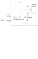
図1は、実施形態1におけるSDRAMコントローラ4内のDMA実行回数決定回路のブロック図である。
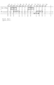
図2は、このような制御を行う場合のDMAコントローラ4全体の動きを示すタイミングチャートである。本例では、バースト長は、予め初期MRSコマンド発行時に、最大値=8に設定しているものとする。
【0047】
また、DMA要求ブロック1−1の最大連続DMA要求数は25回とし、よってBSTNUM_1のバス幅は5とする。
【0048】
処理の流れとして、DMA要求ブロック1−1がアドレス0000Ehから、12回分のバーストリードのDMA要求を発した場合を例とする。
【0049】
T0においてアービタ回路3は、アービトレーション動作許可の状態で、各DMA要求ブロック1からのDMA要求を待っている。
【0050】
T1においてDMA要求ブロック1−1は、DMA制御情報を出力すると同時に、DMA要求信号(DREQ_1)を有効にする。
【0051】
アービタ回路3は、DREQ_1の受信をT2中に確認すると、他のDREQが出力されていないか、さらに他のDREQが出力されている場合には、予め定められた優先順位に基づいて調停及び選択を行い、選択されたDMA要求ブロック1に関するDMA制御情報をラッチする。
【0052】
その後T3にて、選択されたDMA要求ブロック(DMA要求ブロック1−1)に対してDREQACKXを返送する。
【0053】
同時に、SDRAMコントローラ4に対してラッチしたDMA制御情報を出力すると同時に、REQを有効にする。そしてアービタ回路3はDMA要求の受付及び調停、選択の禁止状態に入る。
【0054】
REQを受けたSDRAMコントローラ4は、まずT4にて、ACTVコマンドの発行によってローアドレスを出力する。
【0055】
さらに検出器11により、アドレス[3:1]の下位3ビットから、連続アクセス可能な数=1を検出する。これは、例えば、アドレス[3:1]の3ビットを反転して1加えるなどすれば求められる。これとBSTNUMの値=12とを比較器12で比較すると、連続アクセス可能な数=1の方が小さいので、この比較結果に基づく選択信号に従って、連続アクセス可能な数=1の方をセレクタ13で選択し、実際のバーストアクセス数としてDMA回数設定カウンタ14に設定する。(ここで、本実施形態では、アドレス0はバイトアクセス時に利用されるものとする。かつ、ここでは簡単のため、16bit幅アクセスとする。)
次にT5にて、READコマンドの発行と同時にカラムアドレスを出力する。READの場合、CL(この例ではCL=2とする)分遅れた後、すなわちT7以降SDRAM5よりリードデータが出力されるので、これを取り込む。
【0056】
取り込まれたデータは、一度SDRAMコントローラ4にてラッチされ、各DMA要求ブロック1に返送される。データアクセス中は、これを各DMA要求ブロック1が読み込めるようORG_DTACKXを有効にする。
【0057】
ORG_DTACKXはアービタ回路3に返送され、アービタ回路3はこれを選択されたDMA要求ブロック(DMA要求ブロック1−1)に対して出力、即ちDTACKX_1のみを有効(ローレベル)にする。
【0058】
DMA要求ブロック1−1は、DTACKX_1が有効になると、そのタイミングのRDDATA_1からデータを読み込む。図2においては、T9でのCLKの立ち上がりでデータD1を読み込んでいる。
【0059】
一方SDRAMコントローラ4は、DMA回数設定カウンタ14に設定された回数分(1回分)データアクセスを要求した後、T6でPREコマンドの発行によってバースト動作を中止させる。
【0060】
また、T9にてORG_DTACKX信号を無効(ハイレベル)にする。
【0061】
アービタ回路3は、T10においてORG_DTACKX信号の無効を検出したら、DMA要求の受付、調停、及び選択の禁止状態をT11より解除する。(これ以降アービタ回路3に関する動作は、本実施形態の説明には直接関係が無いので省略する。)
一方DMA要求ブロック1−1は、DTACKX_1が有効となっている期間、内部で保持しているアドレスをカウントアップし、同じく内部で保持しているDMA回数をカウントダウンする。この結果DTACKX_1が無効となった時点で、アドレスは00010hとなり、DMA回数は11となる。
【0062】
ここでDMA要求ブロック1−1は、DMA回数が0になっていないので、再度DMA要求をT11にて出力する。その際のDMA制御情報は、アドレス00010hであり、DMA回数は11である。
【0063】
再びDMA要求を受けたSDRAMコントローラ4は、新たに受信したアドレス00010hより、検出器11にて連続アクセス可能な数=8を求め、これとDMA要求回数=11とを比較器12で比較し、連続アクセス可能な数=8の方をセレクタ13で選択し、実際のバーストアクセス数としてDMA回数設定カウンタ14に設定し、リードDMAを行う。その際ORG_DTACKXを8クロックの間有効にする。この結果、DTACKX1も8クロック間有効になる。
【0064】
DMA要求ブロック1は、前回と同様にアドレスを8カウントアップし、DMA回数を8カウントダウンする。
【0065】
この結果、アドレスは00020hであり、DMA回数は3となる。DMA要求ブロック1は、DMA回数が0になっていないので、再度DMA要求をT28にて出力する。
【0066】
再びDMA要求を受けたSDRAMコントローラ4は、新たに受信したアドレスより連続アクセス可能な数=8を求め、これをDMA要求回数=3と比較する。今回はDMA要求回数の方が小さいため、こちらが選択され、実際のバーストアクセス数を3とし、アクセスを行う。その際ORG_DTACKXを3クロック間有効にし、同様にDTACKX1も3クロック間有効になる。
【0067】
DMA要求ブロック1−1は、前回と同様アドレスを3カウントアップし、DMA回数を3カウントダウンする。
【0068】
この結果、アドレス00026hとなり、DMA回数は0となる。DMA要求ブロック1−1は、DMA回数が0となったので、DMA処理を終了する。
【0069】
このようにして、12回の連続アクセスを3回に分けて実行するので、この間に、他のDMA要求ブロック1がDMA要求を行った場合や、リフレッシュ要求が発生した場合でも、間に割り込むことが可能である。
【0070】
〔実施形態2〕
実施形態1では、BSTNUM信号は、DMA要求ブロックの最大連続DMA要求数によって決まっていた。一方比較器12のサイズは、複数のDMA要求ブロックのうち最も大きな最大連続DMA要求数で決定されるため、1つだけしか大きいものが無い場合でも、そのサイズにあわせる必要があり、回路が冗長的になる可能性がある。
【0071】
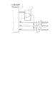
そこで、本実施形態では、比較器12の大きさをSDRAMコントローラ4が実行できる最大のDMA回数にあわせるために、DMA要求ブロック1側でDMA要求回数からDBSTNUM信号を生成する回路を、図3のように構成する。
【0072】
図3は、SDRAMコントローラ4が実行できる最大のDMA回数は8の場合の例を示している(あらかじめMRSコマンドにて設定する)。
【0073】
この場合、DBSTNUM信号バス幅は3で良い(DBSTNUM信号+1=実際のDMA要求回数とする。よって“000”でもDMAを1回行い、“111”でDMAを8回実行する)。
【0074】
そこで、DMA要求回数設定カウンタ31の下位3ビットより上をORゲート32に入力し、その出力をORゲート33〜35により下位3ビットと個別にORする。
【0075】
このような回路構成とすることで、DMA要求回数設定カウンタ31に設定されたバースト要求回数が8以上の場合、ORゲート32の出力は1となり、更にORゲート33〜35の出力も全て1となるので、DBSTNUM信号(DBSTNUM1〜3)は必ず“111”となる。
【0076】
このような構成を持つ各DMA要求ブロック1と、実施形態1で示したSDRAMコントローラ4とを組み合わせることにより、動作的には実施形態1で示したものと変わることなく、かつSDRAMコントローラ4内の比較器も3ビット同士を比較するだけで良くなり、回路の冗長性はなくなる。
【0077】
また、各DMA要求ブロック1とDMAコントローラ2との間のバス幅も最小で済み、ASIC等の集積回路で構成する場合、配線部分の面積を小さくすることが可能となる。
【0078】
【発明の効果】
以上説明したように、本発明によれば、要求されたDMA回数と、与えられたDMA開始アドレスから連続アクセス可能な回数とを比較し、実際に実行するDMA回数を決定するようにしたので、比較的簡単な構成で、実際にSDRAMコントローラが実行可能な連続DMA回数を超える連続DMAを行うことが可能となる。
【0079】
この場合SDRAMコントローラは、実際には、自身が行うことが可能な連続DMAを超えた連続DMAを行うわけではないため、1つのDMA要求ブロックが長時間バスを占有することは無く、比較的低速クロックを利用する電子機器等においても、リフレッシュ等の他の制御を邪魔することは無い。
【0080】
また、1回のバーストDMAは、必ず同一コラム内で行われるため、コラムをまたがるDMAを行うために複雑な制御を行う必要が無く、回路も簡単で済む。
【図面の簡単な説明】
【図1】本発明に係る一実施形態のSDRAMコントローラ内のDMA実行回数決定回路のブロック図である。
【図2】第1の実施形態を説明するためのタイミングチャートである。
【図3】第2の実施形態におけるDMA要求ブロック内のBSTNUM信号生成回路を示した図である。
【図4】標準的なSDRAMへのアクセスを示すタイミングチャートである。
【図5】一般的なDMAコントローラの構成の一例を示したブロック図である。
【図6】従来のDMAコントローラ全体の動きを示すタイミングチャートである。
【符号の説明】
1 DMA要求ブロック
2 DMAコントローラ
3 アービタ回路
4 SDRAMコントローラ
5 SDRAM
11 検出器
12 比較器
13 セレクタ
14 DMA回数設定カウンタ
31 DMA要求回数設定カウンタ
32〜35 ORゲート[0001]
BACKGROUND OF THE INVENTION
The present invention relates to a memory control circuit using SDRAM.
[0002]
[Prior art]
SDRAM is a relatively new device designed to operate asynchronous DRAM at high speed.
[0003]
The control method is similar to that of a conventional asynchronous DRAM, but uses a CLK signal for synchronization, access to the SDRAM is performed by a command, and continuous data read / write is possible (burst mode). , Etc. are characteristic.
[0004]
FIG. 4 is a timing chart showing access to a standard SDRAM. Here, a case where the burst length (BL) = 2 is shown.
[0005]
In the actual access method to the SDRAM, the SDRAM controller first outputs the RAS address simultaneously with the issuance of the ACTV command, and then outputs the CAS address simultaneously with the issuance of the WRITEA or READA command. (In the following description, the next command can be accepted 1 CLK after the ACTV command unless otherwise specified.)
At this time, if it is WRITE, data to be written to the data bus line is simultaneously output and a write operation is performed. In the case of READA, since the read data is output from the SDRAM after being delayed by a specific delay value (CAS LATENCY = CL), it is captured.
[0006]
By the way, when the above WRITE / READA is used, the number of bursts is constant at the value specified by BURST LENGTH (= BL). Therefore, when an arbitrary number of bursts is to be executed, an MRS command is issued. Therefore, it is necessary to change the BL value and control so as to reach the desired number of bursts in combination, and the total throughput is lowered. Therefore, there is a method in which the burst operation is interrupted when the SDRAM controller reaches a desired number of bursts without using the WRITE / READA command.
FIG. 5 is a block diagram showing an example of the configuration of a general DMA controller. In general, the DMA request block has a different configuration depending on the application. On the other hand, since the circuit of the memory controller unit differs depending on the type of memory, the arbitration unit and the memory controller unit are independent from each other in order to facilitate compatibility with various applications and memories. It is better to take the configuration.
[0007]
In this case, each of the DMA request blocks 1-1... 1-N to the arbiter circuit 3 is requested by the DMA request signal DREQ_1... N, the address signal ADDRESS_1. DR-WX_1... N indicating the number of bursts, BSTNUM_1... N indicating the number of bursts, a write data bus WRDATA_1.
[0008]
On the other hand, from the arbiter circuit 3 to each DMA request block 1-1... 1-N, REQACKX_1... N, which is a negative logic DMA request acceptance signal, and RDDATA_1. , DTACKX_1... N signal, which is a negative logic memory access signal, is output.
[0009]
In this description, WRDATA and RDDATA are connected to all DMA request blocks 1-1... 1-N, but each DMA request block actually performs only one of read and write. In some cases, unused data buses need not be connected. In this figure, the circuit for controlling the refresh of the SDRAM is omitted.
[0010]
On the other hand, from the arbiter circuit 3 to the SDRAM controller 4, the DMA request signal REQ after arbitration, the address signal ADRS after arbitration, the read / write identification signal R-WX after arbitration, BSTNUM indicating the number of bursts, and the write data bus A signal such as WRDATA is output. On the other hand, the SDRAM controller 4 outputs the read data bus RDDATA and the negative logic memory access signal ORG_DTACKX to the arbiter circuit 3. By adopting the above-described configuration and unifying the interface between the arbiter circuit 3 and the memory controller unit 4, it becomes easy to deal with various applications and memories.
[0011]
FIG. 6 is a timing chart showing the movement of the entire DMA controller when such control is performed. In this example, the burst length is set to a maximum value = 8 in advance when the initial MRS command is issued.
[0012]
This figure also shows a case where the DMA request block 1-1 first issues a burst read DMA request alone and the DMA request block 1-2 issues a burst write DMA request during DMA processing.
[0013]
The detailed control flow is as follows.
[0014]
At T0, the arbiter circuit waits for a DMA request from each DMA request block with the arbitration operation permitted.
[0015]
At T1, the DMA request block 1-1 outputs the DMA control information and at the same time enables the DREQ. (Here, it is assumed that
[0016]
Thereafter, at T3, DREQACKX is returned to the selected DMA request block (DMA request block 1).
[0017]
At the same time, the latched DMA control information is output to the SDRAM controller 4, and at the same time, the REQ is validated. The arbiter circuit 3 enters a DMA request acceptance, arbitration, and selection prohibited state.
[0018]
Upon receiving the REQ, the SDRAM controller 4 first outputs a row address by issuing an ACTV command at T4, and then outputs a column address at the same time as issuing a READ command at T5. In the case of READ, after a delay of CL (in this example, CL = 2), that is, after T7, read data is output from the SDRAM 5 onto the DQ, and this is captured. In this example, when the command is not issued, the NOP state is set. However, it is possible to wait in a state such as DESL or PD.
[0019]
The fetched data is once latched by the SDRAM controller 4 and returned to each
[0020]
ORG_DTACKX is returned to the arbiter circuit, and the arbiter circuit makes it valid for the selected DMA request block (DMA request block 1), that is, only DTACKX_1.
[0021]
When DTACKX_1 becomes valid, the
[0022]
On the other hand, the SDRAM controller 4 requests data access for a desired number of times (twice), and then stops the burst operation by issuing a PRE command at T7.
[0023]
Further, when the desired number of times (two times) of data is read, the ORG_DTACKX signal is invalidated (high level) at T9.
[0024]
When the arbiter circuit 3 detects the rising edge of the ORG_DTACKX signal at T10, the arbiter circuit 3 cancels the DMA request acceptance, arbitration, and selection prohibited states at T11.
[0025]
As a result, DREQ2 of the DMA request block 1-2 is recognized at T12, and when another DREQ is not output or another DREQ is output, based on a predetermined priority order, Perform mediation and selection.
[0026]
In this example, since there is only a request from the DMA request block 1-2, the DMA control information from the DMA request block 1-2 is latched.
[0027]
Thereafter, at T13, DREQACKX is returned to the selected DMA request block (DMA request block 1-2).
[0028]
At the same time, the latched DMA control information is output to the SDRAM controller 4 to enable REQ. The arbiter circuit 3 again enters the DMA request acceptance, arbitration, and selection prohibited state.
[0029]
Upon receiving the REQ, the SDRAM controller 4 first outputs a row address by issuing an ACTV command at T14, and then outputs a column address simultaneously with the issuance of the WRIT command at T15.
[0030]
In the case of WRIT, the DMA request block 1-2 outputs data to the WRDATA_2 bus at the same timing as when the WRIT command is issued.
[0031]
This data is output to the DQ via the SDRAM controller 4 and actually written to the memory. ORG_DTACKX is valid while it is being written to memory.
[0032]
ORG_DTACKX is returned to the arbiter circuit 3, and the arbiter circuit 3 validates only the DTACKX_2 for the selected DMA request block (DMA request block 1-2).
[0033]
In this example, since burst write is performed three times, when data for three times is written, a PRE command is issued at T18 to interrupt the burst write and disable ORG_DTACKX.
[0034]
When the arbiter circuit 3 detects the rising edge of the ORG_DTACKX signal at T18, the arbiter circuit 3 cancels the DMA request acceptance, arbitration, and selection prohibited states from T19.
[0035]
[Problems to be solved by the invention]
In the above conventional control method, the maximum number of continuous accesses to the SDRAM is limited by the setting to the SDRAM, and the value is 256, 8, 4, 2 in a general SDRAM.
[0036]
Furthermore, there is a special relationship between burst length and address. When burst access is performed in the SDRAM, the address is updated by a counter in the SDRAM. However, the address count-up does not carry over the set burst length, so even if continuous access is made from any address, different addresses are accessed. For example, when the burst length is set to 8, even if an attempt is made to access the lower addresses from 0Ch to 14h in 5 bursts, in reality, 0Ch, 0Eh, 00, 02, 04 are accessed.
[0037]
On the other hand, in an electronic device such as a printer, the maximum continuous DMA request is about 10 to 100. Also, since the installed memory capacity is not large, it is difficult to construct a system that allows access from a place where column address separation is good.
[0038]
In order to deal with such a problem, Japanese Patent Laid-Open No. 2000-215155 describes a control in which single transfer is performed up to a good break and then burst transfer is performed, but this makes the circuit complicated. There is a problem that becomes.
[0039]
Furthermore, the number of DMA request blocks is about 10, and if one DMA request block is continuously accessed for a long time, the other DMA request blocks cannot be processed, resulting in a problem such as a slow throughput in the printer. .
[0040]
In these electronic devices, the supply clock to the SDRAM is considerably smaller than the maximum clock frequency that can be received by the SDRAM. If one DMA request block is continuously accessed for a long time, the memory cannot be refreshed. Yes.
[0041]
Therefore, in these electronic devices, there has been a demand for a memory control system capable of starting continuous access exceeding 8 bursts from an arbitrary address with a relatively simple configuration.
[0042]
[Means for Solving the Problems]
In order to cope with the above-mentioned problems, the present invention is a system using an SDRAM, which is operated with a clock slower than the standard operation clock of the SDRAM, and is continuously accessed from an arbitrary address by a relatively simple circuit. The object is to provide a possible memory control system.
[0043]
In order to solve the above-described problem, according to the present invention, a memory including a plurality of DMA request blocks and a memory control circuit that executes access to the SDRAM based on the DMA requests received from the plurality of DMA request blocks. In the access system, the memory control circuit receives a DMA control information signal including an address signal and an instruction signal indicating the number of burst DMA requests together with the DMA request, and continuous access based on the address signal. Detecting means for detecting the possible number of times, selecting means for selecting the lesser of the number of burst DMA requests indicated by the instruction signal and the number of continuously accessible times detected by the detecting means, and the selection A setting method for setting the number of times selected by the means as the number of continuous DMAs to be actually executed. And each of the plurality of DMA request blocks has the burst DMA request count as the burst DMA request count as it is if the burst DMA request count is equal to or less than the maximum number of times that the memory control circuit can continuously access. If the value is larger than the maximum value, a generation means for generating an instruction signal for instructing the maximum value as the number of burst DMA requests, and a memory address signal for designating an access destination are generated by a data access signal from the memory control circuit. Count-up means for counting up, count-down means for counting down the number of burst DMA requests by the data access signal, and when one burst DMA control is completed by the data access signal, the number of burst DMA requests counted down is 0. Whether or not If the number of burst DMA requests counted down is not 0 as a result of determination by the determination unit, the generation unit calculates the memory address signal counted up and the number of burst DMA requests counted down by the generation unit. Request control means for controlling to make a DMA request again based on the generated instruction signal.
[0044]
DETAILED DESCRIPTION OF THE INVENTION
Hereinafter, an embodiment of the present invention will be described in detail with reference to the drawings.
[0045]
In this embodiment, the overall configuration of the DMA controller has the general configuration shown in FIG. 5 used for the description of the prior art. The present embodiment is characterized by a configuration in the SDRAM controller 4.
[0046]
FIG. 1 is a block diagram of a DMA execution frequency determination circuit in the SDRAM controller 4 according to the first embodiment.
FIG. 2 is a timing chart showing the overall movement of the DMA controller 4 when such control is performed. In this example, it is assumed that the burst length is set to a maximum value = 8 in advance when the initial MRS command is issued.
[0047]
In addition, the maximum number of consecutive DMA requests in the DMA request block 1-1 is 25, so that the bus width of BSTNUM_1 is 5.
[0048]
As an example of processing flow, the DMA request block 1-1 issues a burst read DMA request for 12 times from the address 0000Eh.
[0049]
At T0, the arbiter circuit 3 waits for a DMA request from each
[0050]
At T1, the DMA request block 1-1 outputs the DMA control information and at the same time validates the DMA request signal (DREQ_1).
[0051]
When the arbiter circuit 3 confirms reception of DREQ_1 during T2, if no other DREQ is output or if another DREQ is output, arbitration and selection are performed based on a predetermined priority order. And the DMA control information related to the selected
[0052]
Thereafter, at T3, DREQACKX is returned to the selected DMA request block (DMA request block 1-1).
[0053]
At the same time, the latched DMA control information is output to the SDRAM controller 4, and at the same time, the REQ is validated. The arbiter circuit 3 enters a DMA request acceptance, arbitration, and selection prohibited state.
[0054]
Upon receiving the REQ, the SDRAM controller 4 first outputs a row address by issuing an ACTV command at T4.
[0055]
Further, the
Next, at T5, the column address is output simultaneously with the issuance of the READ command. In the case of READ, read data is output after being delayed by CL (in this example, CL = 2), that is, read data is output from SDRAM 5 after T7.
[0056]
The fetched data is once latched by the SDRAM controller 4 and returned to each
[0057]
ORG_DTACKX is returned to the arbiter circuit 3, and the arbiter circuit 3 outputs it to the selected DMA request block (DMA request block 1-1), that is, makes only DTACKX_1 valid (low level).
[0058]
When DTACKX_1 becomes valid, the DMA request block 1-1 reads data from RDDATA_1 at that timing. In FIG. 2, data D1 is read at the rising edge of CLK at T9.
[0059]
On the other hand, after requesting data access for the number of times (one time) set in the DMA
[0060]
At T9, the ORG_DTACKX signal is invalidated (high level).
[0061]
When the arbiter circuit 3 detects that the ORG_DTACKX signal is invalid at T10, the arbiter circuit 3 cancels the DMA request acceptance, arbitration, and selection prohibition states from T11. (Hereafter, the operation relating to the arbiter circuit 3 is omitted because it is not directly related to the description of the present embodiment.)
On the other hand, the DMA request block 1-1 counts up the address held internally during the period when DTACKX_1 is valid, and counts down the number of DMAs held in the same. As a result, when DTACKX_1 becomes invalid, the address becomes 00010h and the DMA count becomes 11.
[0062]
Here, the DMA request block 1-1 outputs the DMA request again at T11 because the DMA count is not zero. The DMA control information at that time is address 00010h and the DMA count is 11.
[0063]
The SDRAM controller 4 that has received the DMA request again obtains the number = 8 that can be continuously accessed by the
[0064]
The
[0065]
As a result, the address is 0,020h and the DMA count is 3. Since the DMA count is not 0, the
[0066]
The SDRAM controller 4 which has received the DMA request again obtains the number of continuously accessible = 8 from the newly received address, and compares this with the number of DMA requests = 3. Since the number of DMA requests is smaller this time, this is selected, and the actual number of burst accesses is set to 3 for access. At this time, ORG_DTACKX is enabled for 3 clocks, and DTACKX1 is also enabled for 3 clocks.
[0067]
The DMA request block 1-1 increments the address by 3 as in the previous time, and decrements the DMA count by 3.
[0068]
As a result, the address becomes 00002h and the DMA count becomes 0. The DMA request block 1-1 ends the DMA process because the DMA count has become zero.
[0069]
In this way, twelve consecutive accesses are executed in three steps, so even if another
[0070]
[Embodiment 2]
In the first embodiment, the BSTNUM signal is determined by the maximum number of consecutive DMA requests in the DMA request block. On the other hand, the size of the
[0071]
Therefore, in the present embodiment, in order to adjust the size of the
[0072]
FIG. 3 shows an example in which the maximum number of DMAs that can be executed by the SDRAM controller 4 is 8 (set in advance by an MRS command).
[0073]
In this case, the DBSTNUM signal bus width may be 3 (DBSTNUM signal + 1 + 1 = actual DMA request count. Therefore, even if “000”, DMA is performed once, and “111” is performed DMA eight times).
[0074]
Therefore, the upper three bits of the DMA request
[0075]
With such a circuit configuration, when the number of burst requests set in the DMA request
[0076]
By combining each
[0077]
In addition, the bus width between each
[0078]
【The invention's effect】
As described above, according to the present invention, the requested number of DMAs is compared with the number of continuous accesses from the given DMA start address, and the number of DMAs to be actually executed is determined. With a relatively simple configuration, it is possible to perform continuous DMA exceeding the number of continuous DMAs that can be actually executed by the SDRAM controller.
[0079]
In this case, the SDRAM controller does not actually perform continuous DMA exceeding the continuous DMA that can be performed by itself, so that one DMA request block does not occupy the bus for a long time and is relatively slow. Even in an electronic device using a clock, other controls such as refresh are not disturbed.
[0080]
In addition, since one burst DMA is always performed in the same column, it is not necessary to perform complicated control in order to perform DMA across columns, and the circuit is simple.
[Brief description of the drawings]
FIG. 1 is a block diagram of a DMA execution frequency determination circuit in an SDRAM controller according to an embodiment of the present invention.
FIG. 2 is a timing chart for explaining the first embodiment;
FIG. 3 is a diagram showing a BSTNUM signal generation circuit in a DMA request block in the second embodiment.
FIG. 4 is a timing chart showing access to a standard SDRAM.
FIG. 5 is a block diagram showing an example of a configuration of a general DMA controller.
FIG. 6 is a timing chart showing the overall movement of a conventional DMA controller.
[Explanation of symbols]
1
11
Claims (2)
前記メモリ制御回路が、
前記DMA要求とともに、アドレス信号と、バーストDMA要求回数を指示する指示信号とを含むDMA制御情報信号を受信する受信手段と、
前記アドレス信号に基づいて連続アクセス可能な回数を検出する検出手段と、
前記指示信号により指示されたバーストDMA要求回数と前記検出手段により検出された連続アクセス可能な回数とのうちで大きくない方を選択する選択手段と、
前記選択手段により選択された回数を、実際に実行する連続DMAの回数として設定する設定手段とを有し、
前記複数のDMA要求ブロックのそれぞれが、
バーストDMA要求回数が前記メモリ制御回路が連続アクセス可能な回数の最大値以下であれば、当該バーストDMA要求回数をそのままバーストDMA要求回数として指示し、前記最大値より大きい場合は、当該最大値をバーストDMA要求回数として指示する指示信号を生成する生成手段と、
アクセス先を指定するメモリアドレス信号を前記メモリ制御回路からのデータアクセス信号によりカウントアップするカウントアップ手段と、
バーストDMA要求回数を前記データアクセス信号によりカウントダウンするカウントダウン手段と、
前記データアクセス信号により1回のバーストDMA制御が終了した時点で、カウントダウンされたバーストDMA要求回数が0か否かを判定する判定手段と、
前記判定手段による判定の結果、前記カウントダウンされたバーストDMA要求回数が0でない場合に、カウントアップされた前記メモリアドレス信号と、当該カウントダウンされたバーストDMA要求回数から前記生成手段によって生成される指示信号とに基づいて、再度DMA要求を行うように制御する要求制御手段とを有することを特徴とするメモリアクセスシステム。 A memory access system comprising a plurality of DMA request blocks and a memory control circuit for executing access to the SDRAM based on DMA requests received from the plurality of DMA request blocks,
The memory control circuit is
Receiving means for receiving, together with the DMA request, a DMA control information signal including an address signal and an instruction signal indicating the number of burst DMA requests;
Detecting means for detecting the number of continuous accesses based on the address signal;
Selecting means for selecting a lesser one of the number of burst DMA requests indicated by the instruction signal and the number of continuously accessible times detected by the detecting means;
The number of times selected by the selection means, have a setting means for setting a number of consecutive DMA actually executing,
Each of the plurality of DMA request blocks is
If the burst DMA request count is less than or equal to the maximum number of times that the memory control circuit can continuously access, the burst DMA request count is indicated as it is as the burst DMA request count, and if it is greater than the maximum value, the maximum value is set. Generating means for generating an instruction signal indicating the number of burst DMA requests;
Count-up means for counting up a memory address signal designating an access destination by a data access signal from the memory control circuit;
Countdown means for counting down the number of burst DMA requests by the data access signal;
Determining means for determining whether or not the number of burst DMA requests counted down is zero when one burst DMA control is terminated by the data access signal;
If the number of burst DMA requests counted down is not 0 as a result of determination by the determination unit, the memory address signal counted up and an instruction signal generated by the generation unit from the number of burst DMA requests counted down based on the bets, a memory access system characterized by having a request control means for controlling to perform DMA request.
Priority Applications (3)
| Application Number | Priority Date | Filing Date | Title |
|---|---|---|---|
| JP2002123811A JP4054598B2 (en) | 2002-04-25 | 2002-04-25 | Memory control circuit, DMA request block, and memory access system |
| US10/417,087 US6859848B2 (en) | 2002-04-25 | 2003-04-17 | Circuit for controlling sequential access to SDRAM |
| CN03123280.9A CN1231844C (en) | 2002-04-25 | 2003-04-25 | Circuit of controlling continuous access to SDRAM |
Applications Claiming Priority (1)
| Application Number | Priority Date | Filing Date | Title |
|---|---|---|---|
| JP2002123811A JP4054598B2 (en) | 2002-04-25 | 2002-04-25 | Memory control circuit, DMA request block, and memory access system |
Publications (3)
| Publication Number | Publication Date |
|---|---|
| JP2003316642A JP2003316642A (en) | 2003-11-07 |
| JP2003316642A5 JP2003316642A5 (en) | 2005-09-29 |
| JP4054598B2 true JP4054598B2 (en) | 2008-02-27 |
Family
ID=29243698
Family Applications (1)
| Application Number | Title | Priority Date | Filing Date |
|---|---|---|---|
| JP2002123811A Expired - Fee Related JP4054598B2 (en) | 2002-04-25 | 2002-04-25 | Memory control circuit, DMA request block, and memory access system |
Country Status (3)
| Country | Link |
|---|---|
| US (1) | US6859848B2 (en) |
| JP (1) | JP4054598B2 (en) |
| CN (1) | CN1231844C (en) |
Families Citing this family (7)
| Publication number | Priority date | Publication date | Assignee | Title |
|---|---|---|---|---|
| US7107365B1 (en) * | 2002-06-25 | 2006-09-12 | Cypress Semiconductor Corp. | Early detection and grant, an arbitration scheme for single transfers on AMBA advanced high-performance bus |
| US7899957B1 (en) * | 2003-12-30 | 2011-03-01 | Altera Corporation | Memory controller having a buffer for providing beginning and end data |
| WO2008084017A1 (en) * | 2007-01-05 | 2008-07-17 | Proton World International N.V. | Limitation of access to a resource of an electronic circuit |
| JP5064336B2 (en) * | 2008-09-12 | 2012-10-31 | 株式会社リコー | Image forming system and program |
| KR101989860B1 (en) | 2012-12-21 | 2019-06-17 | 에스케이하이닉스 주식회사 | Memory controller and memory system including the same |
| JP6210018B2 (en) * | 2014-04-25 | 2017-10-11 | 株式会社オートネットワーク技術研究所 | Switch ON / OFF control method and switch circuit |
| JP6316143B2 (en) * | 2014-08-22 | 2018-04-25 | ルネサスエレクトロニクス株式会社 | Semiconductor device, memory access control method, and semiconductor device system |
Family Cites Families (4)
| Publication number | Priority date | Publication date | Assignee | Title |
|---|---|---|---|---|
| JPH10133998A (en) | 1996-11-05 | 1998-05-22 | Canon Inc | Data processing method and recorder using the method |
| US6366989B1 (en) * | 1998-09-17 | 2002-04-02 | Sun Microsystems, Inc. | Programmable memory controller |
| JP3976927B2 (en) | 1999-01-25 | 2007-09-19 | キヤノン株式会社 | Bus control device |
| US6622203B2 (en) * | 2001-05-29 | 2003-09-16 | Agilent Technologies, Inc. | Embedded memory access method and system for application specific integrated circuits |
-
2002
- 2002-04-25 JP JP2002123811A patent/JP4054598B2/en not_active Expired - Fee Related
-
2003
- 2003-04-17 US US10/417,087 patent/US6859848B2/en not_active Expired - Lifetime
- 2003-04-25 CN CN03123280.9A patent/CN1231844C/en not_active Expired - Fee Related
Also Published As
| Publication number | Publication date |
|---|---|
| CN1231844C (en) | 2005-12-14 |
| US20030204651A1 (en) | 2003-10-30 |
| JP2003316642A (en) | 2003-11-07 |
| CN1462946A (en) | 2003-12-24 |
| US6859848B2 (en) | 2005-02-22 |
Similar Documents
| Publication | Publication Date | Title |
|---|---|---|
| US6104417A (en) | Unified memory computer architecture with dynamic graphics memory allocation | |
| US6477598B1 (en) | Memory controller arbitrating RAS, CAS and bank precharge signals | |
| US20020007435A1 (en) | Methods and apparatus for variable length SDRAM transfers | |
| JP3819004B2 (en) | Memory control device | |
| US7373453B2 (en) | Method and apparatus of interleaving memory bank in multi-layer bus system | |
| JP4054598B2 (en) | Memory control circuit, DMA request block, and memory access system | |
| JP2003015949A (en) | Control device for semiconductor storage device and control method for semiconductor storage device | |
| US5802581A (en) | SDRAM memory controller with multiple arbitration points during a memory cycle | |
| JPH10228413A (en) | Memory access controlling method device therefor and memory system | |
| US7310717B2 (en) | Data transfer control unit with selectable transfer unit size | |
| US5802597A (en) | SDRAM memory controller while in burst four mode supporting single data accesses | |
| US6529981B1 (en) | Bus arbiter | |
| JPH0793274A (en) | System and device for transferring data | |
| US6948046B2 (en) | Access controller that efficiently accesses synchronous semiconductor memory device | |
| JP4108237B2 (en) | Memory control device | |
| JP2013105428A (en) | Signal transfer circuit | |
| JP2002366509A (en) | Direct memory access controller and its access control method | |
| JP2002334050A (en) | Circuit and method for memory control | |
| JP2007323113A (en) | Memory control circuit | |
| JP2000242544A (en) | Memory controller and direct memory access controller | |
| JPH06325570A (en) | Dynamic memory refresh circuit | |
| JP3563340B2 (en) | Memory controller | |
| KR100690597B1 (en) | Single mode direct memory access application method using cpu applying dual mode direct memory access | |
| KR100210404B1 (en) | An apparatus for controlling access of memory in dual bus system | |
| JPH09297990A (en) | Memory refresh control method and memory refresh controller |
Legal Events
| Date | Code | Title | Description |
|---|---|---|---|
| A521 | Request for written amendment filed |
Free format text: JAPANESE INTERMEDIATE CODE: A523 Effective date: 20050425 |
|
| A621 | Written request for application examination |
Free format text: JAPANESE INTERMEDIATE CODE: A621 Effective date: 20050425 |
|
| A977 | Report on retrieval |
Free format text: JAPANESE INTERMEDIATE CODE: A971007 Effective date: 20070820 |
|
| A131 | Notification of reasons for refusal |
Free format text: JAPANESE INTERMEDIATE CODE: A131 Effective date: 20070828 |
|
| A521 | Request for written amendment filed |
Free format text: JAPANESE INTERMEDIATE CODE: A523 Effective date: 20071029 |
|
| TRDD | Decision of grant or rejection written | ||
| A01 | Written decision to grant a patent or to grant a registration (utility model) |
Free format text: JAPANESE INTERMEDIATE CODE: A01 Effective date: 20071204 |
|
| A61 | First payment of annual fees (during grant procedure) |
Free format text: JAPANESE INTERMEDIATE CODE: A61 Effective date: 20071210 |
|
| FPAY | Renewal fee payment (event date is renewal date of database) |
Free format text: PAYMENT UNTIL: 20101214 Year of fee payment: 3 |
|
| R150 | Certificate of patent or registration of utility model |
Ref document number: 4054598 Country of ref document: JP Free format text: JAPANESE INTERMEDIATE CODE: R150 Free format text: JAPANESE INTERMEDIATE CODE: R150 |
|
| FPAY | Renewal fee payment (event date is renewal date of database) |
Free format text: PAYMENT UNTIL: 20111214 Year of fee payment: 4 |
|
| FPAY | Renewal fee payment (event date is renewal date of database) |
Free format text: PAYMENT UNTIL: 20121214 Year of fee payment: 5 |
|
| FPAY | Renewal fee payment (event date is renewal date of database) |
Free format text: PAYMENT UNTIL: 20131214 Year of fee payment: 6 |
|
| LAPS | Cancellation because of no payment of annual fees |