JP4032857B2 - Glass substrate for touch panel, touch panel and portable terminal - Google Patents
Glass substrate for touch panel, touch panel and portable terminal Download PDFInfo
- Publication number
- JP4032857B2 JP4032857B2 JP2002215760A JP2002215760A JP4032857B2 JP 4032857 B2 JP4032857 B2 JP 4032857B2 JP 2002215760 A JP2002215760 A JP 2002215760A JP 2002215760 A JP2002215760 A JP 2002215760A JP 4032857 B2 JP4032857 B2 JP 4032857B2
- Authority
- JP
- Japan
- Prior art keywords
- glass substrate
- touch panel
- glass
- laser
- cut
- Prior art date
- Legal status (The legal status is an assumption and is not a legal conclusion. Google has not performed a legal analysis and makes no representation as to the accuracy of the status listed.)
- Expired - Lifetime
Links
Images


Classifications
-
- C—CHEMISTRY; METALLURGY
- C03—GLASS; MINERAL OR SLAG WOOL
- C03B—MANUFACTURE, SHAPING, OR SUPPLEMENTARY PROCESSES
- C03B33/00—Severing cooled glass
- C03B33/09—Severing cooled glass by thermal shock
-
- C—CHEMISTRY; METALLURGY
- C03—GLASS; MINERAL OR SLAG WOOL
- C03B—MANUFACTURE, SHAPING, OR SUPPLEMENTARY PROCESSES
- C03B33/00—Severing cooled glass
- C03B33/02—Cutting or splitting sheet glass or ribbons; Apparatus or machines therefor
- C03B33/023—Cutting or splitting sheet glass or ribbons; Apparatus or machines therefor the sheet or ribbon being in a horizontal position
- C03B33/033—Apparatus for opening score lines in glass sheets
-
- C—CHEMISTRY; METALLURGY
- C03—GLASS; MINERAL OR SLAG WOOL
- C03B—MANUFACTURE, SHAPING, OR SUPPLEMENTARY PROCESSES
- C03B33/00—Severing cooled glass
- C03B33/07—Cutting armoured, multi-layered, coated or laminated, glass products
-
- C—CHEMISTRY; METALLURGY
- C03—GLASS; MINERAL OR SLAG WOOL
- C03B—MANUFACTURE, SHAPING, OR SUPPLEMENTARY PROCESSES
- C03B33/00—Severing cooled glass
- C03B33/09—Severing cooled glass by thermal shock
- C03B33/091—Severing cooled glass by thermal shock using at least one focussed radiation beam, e.g. laser beam
-
- Y—GENERAL TAGGING OF NEW TECHNOLOGICAL DEVELOPMENTS; GENERAL TAGGING OF CROSS-SECTIONAL TECHNOLOGIES SPANNING OVER SEVERAL SECTIONS OF THE IPC; TECHNICAL SUBJECTS COVERED BY FORMER USPC CROSS-REFERENCE ART COLLECTIONS [XRACs] AND DIGESTS
- Y02—TECHNOLOGIES OR APPLICATIONS FOR MITIGATION OR ADAPTATION AGAINST CLIMATE CHANGE
- Y02P—CLIMATE CHANGE MITIGATION TECHNOLOGIES IN THE PRODUCTION OR PROCESSING OF GOODS
- Y02P40/00—Technologies relating to the processing of minerals
- Y02P40/50—Glass production, e.g. reusing waste heat during processing or shaping
- Y02P40/57—Improving the yield, e-g- reduction of reject rates
-
- Y—GENERAL TAGGING OF NEW TECHNOLOGICAL DEVELOPMENTS; GENERAL TAGGING OF CROSS-SECTIONAL TECHNOLOGIES SPANNING OVER SEVERAL SECTIONS OF THE IPC; TECHNICAL SUBJECTS COVERED BY FORMER USPC CROSS-REFERENCE ART COLLECTIONS [XRACs] AND DIGESTS
- Y10—TECHNICAL SUBJECTS COVERED BY FORMER USPC
- Y10T—TECHNICAL SUBJECTS COVERED BY FORMER US CLASSIFICATION
- Y10T428/00—Stock material or miscellaneous articles
- Y10T428/24—Structurally defined web or sheet [e.g., overall dimension, etc.]
- Y10T428/24355—Continuous and nonuniform or irregular surface on layer or component [e.g., roofing, etc.]
-
- Y—GENERAL TAGGING OF NEW TECHNOLOGICAL DEVELOPMENTS; GENERAL TAGGING OF CROSS-SECTIONAL TECHNOLOGIES SPANNING OVER SEVERAL SECTIONS OF THE IPC; TECHNICAL SUBJECTS COVERED BY FORMER USPC CROSS-REFERENCE ART COLLECTIONS [XRACs] AND DIGESTS
- Y10—TECHNICAL SUBJECTS COVERED BY FORMER USPC
- Y10T—TECHNICAL SUBJECTS COVERED BY FORMER US CLASSIFICATION
- Y10T428/00—Stock material or miscellaneous articles
- Y10T428/24—Structurally defined web or sheet [e.g., overall dimension, etc.]
- Y10T428/24479—Structurally defined web or sheet [e.g., overall dimension, etc.] including variation in thickness
- Y10T428/24488—Differential nonuniformity at margin
Description
【0001】
【発明の属する技術分野】
本発明は、特にレーザ光の照射及び強制冷却により切断されて成るタッチパネル用ガラス基板、タッチパネル及び携帯端末に係わる。
【0002】
【従来の技術】
一般に、ガラス原板を縦横に切断して所定の幅及び長さを有するガラス基板を形成するガラスの切断方法としては、例えば特開平11−71124号公開公報に形成されるような機械式、またレーザ光を照射するレーザ式などが用いられている。
【0003】
機械式加工による切断方法をとる場合、ガラスに刃が加圧して、メジアンクラック即ちガラス面に垂直な方向に伸びるクラックを生じさせて切断を行っている。この切断方法では、刃の除圧工程において切り開かれたガラス切断面同士が接触することによって、ラテラルクラック即ちガラス面に水平方向に伸びるクラックが発生する。
【0004】
このため、機械式のガラス切断加工においては切断面に発生するマイクロクラック、すなわちラテラルクラックを完全に防ぐことは不可能であった。クラック即ちひびが生じると、このひびの発生により粉砕粉いわゆるカレットが生じ、カレットが表示体の表面に付着して視認性を損なったり、またガラス基板をタッチパネルに使用する場合などにおいて、透明導電層に付着して短絡を生じさせてしまうなどの不都合を生じる。
このようなラテラルクラックを化学処理により低減化する方法もあるが、生産性の低下を招き、またコストの増大化を招来してしまう。また、化学処理によってガラスの強度にばらつきが生じてしまうという問題がある。
【0005】
一方、レーザ式による場合、例えば特開平8−217478号公開公報、特開平11−254172号公開公報などに炭酸ガスレーザによる加熱切断方法が提案されている。
しかしながら、通常のレーザ光照射のみによる切断方法による場合、図8にその一例の模式的な断面構成を示すように、ガラス基板1のレーザ光照射による切断側面において、そのレーザ光を照射する側から生じるレーザ痕2に微小なひび及びカレットが生じてしまうという問題がある。
【0006】
これに対し、炭酸ガスレーザ等のレーザ光照射による加熱と、水ないしは圧縮空気を用いた強制冷却の複合作用によって、ガラス中に熱歪みを発生させてガラス分断のトリガとして切断を行う方法が提案されている。
特に、近年簡便な入力方法として各種表示体の表面に取り付けられて利用されるタッチパネルや、これを用いた携帯端末に用いられる1.1mm以下、例えば0.3〜0.7mm程度の厚さとされる薄型のガラス基板を切断するにあたって、このレーザ光照射及び強制冷却による切断方法が注目されている。
この方式は、機械的な力が加わらない為、マイクロクラックの発生が殆どないことが利点とされている。
【0007】
【発明が解決しようとする課題】
しかしながらこのようなレーザ光照射及び強制冷却を行う場合においても、図9Aに模式的に示すように、例えばガラス原板10に対し破線x1の位置で示す横方向と、破線y1及びy2で示す縦方向にレーザ光を照射及び強制冷却を行って切断を行うと、レーザ光を縦横に照射する交差点aにおいて、図9Bに示すようにバリ11や欠け12が生じてしまうという問題があった。
この交差点aにおいては、図9Cに示すように切断面が垂直となることが望ましいが、実際には切断面が傾斜したり湾曲したりしてしまい、寸法精度の悪化を招来し、生産性及び歩留りの低下、更にはコストの増大化が問題となっている。
【0008】
本発明は、ガラス原板から所定の寸法のガラス基板を切断するにあたって、上述したようなその切断面におけるひび、欠けが生じず、従ってこの部分からの粉砕粉の発生を回避し、更に強度特性にも優れたタッチパネル用ガラス基板、タッチパネル及び携帯端末を提供することを目的とする。
【0009】
【課題を解決するための手段】
本発明は、少なくともレーザ光の照射により切断されて成るタッチパネル用のガラス基板であって、ガラス基板の切断側面の表面粗さが50nm以下であり、切断側面のレーザ痕の深さを0.06mm以上とし、静荷重試験による強度が55kgf以上90kgf以下として構成する。
また本発明は、上述の構成において、レーザ痕の深さを、ガラス基板の第1の切断側面と、この第1の切断側面とは異なる第2の切断側面とにおいて異なる構成とする。
【0010】
更に本発明は、上述のレーザ痕の深さを、第1及び第2の切断側面において、2%以上異ならせる構成とする。
【0011】
また更に本発明は、上述の各構成において、レーザ痕が、ガラス基板の第1の切断側面において、このガラス基板の第1の主面から所定の深さをもって形成され、第1の切断側面とは異なる第2の切断側面において、第1の主面の裏面である第2の主面から所定の深さをもって形成される構成とする。
【0012】
例えば、ガラス原板に対し、レーザ光の照射及び強制冷却を行うガラスの切断方法にあって、ガラス原板に対する第1の切断方向と、この第1の切断方向とは異なる第2の切断方向とにおいて、レーザ光のレーザパワー又は送り速度を変えて切断を行う。
また、上述のガラスの切断方法において、レーザ光のレーザパワー又は送り速度を、第1の切断方向と第2の切断方向とにおいて4%以上変える。
【0013】
更に、ガラス原板に対し、レーザ光の照射及び強制冷却を行うガラスの切断方法にあって、ガラス原板に対する第1の切断方向の切断を、ガラス原板の第1の主面からレーザ光を照射して行い、ガラス原板に対する第1の切断方向とは異なる第2の切断方向の切断を、第1の主面の裏面である第2の主面からレーザ光を照射して行う。
【0014】
また更に本発明は、上述の構成によるタッチパネル用のガラス基板を、ガラス基板上に光透過性導電層が形成され、このガラス基板とは所定の間隔をもってフィルム基材が対向配置されて成るタッチパネルに用いる構成とする。
更に本発明は、上述の構成によるタッチパネル用のガラス基板を、タッチパネルを有する携帯端末に用いる構成とする。
【0015】
上述したように、レーザ光の照射及び強制冷却を行うガラスの切断方法において、ガラス基板の第1の切断側面と第2の切断側面とにおいて、レーザ痕の深さが異なるように、レーザパワー又はレーザ光の送り速度を異ならしめて照射し、その直後に強制冷却を行って切断することによって、第1及び第2の切断側面の交差部においてひび、バリの発生を回避することができ、所望の寸法精度をもってガラス基板を切断することができた。
【0016】
更に、ガラス基板の第1の切断方向による切断と、第2の切断方向による切断とを、それぞれガラス基板の異なる主面(表面と裏面)からレーザ光を照射して行うことによって、いわば異なる切断側面においてレーザ痕を上下に分離させて切断することによって、同様に第1及び第2の切断側面の交差部においてひび、バリの発生を回避することができ、所望の寸法精度をもってガラス基板を切断することができた。
【0017】
これは、レーザ光照射による加熱と、その後の強制冷却によって生じる歪みの応力を、切断側面の交差部において2方向に生じさせることを回避し、ガラス切断の垂直方向、即ちガラス基板の主面と垂直な方向のみに応力を生じさせて切断を行わしめることができたためと思われる。
【0018】
このようなガラスの切断方法によれば、切断側面の表面の粗さが50nm以下とされ、側面の化学処理が不要なガラス基板を得ることができ、またその静荷重測定による強度を55kgf以上の保持することができた。
しかも、ひび及びバリが生じることなく、所望の寸法精度の薄型のガラス基板を生産性、歩留り良く製造することができて、タッチパネルや携帯端末に本発明によるガラス基板を用いる場合は、生産性、歩留りの向上及びコストの低減化をはかることができる。
【0019】
【発明の実施の形態】
以下、本発明によるガラス基板及びガラスの切断方法の実施の形態とこれに基づく実施例及び比較例を、図面を参照して詳細に説明する。以下の例においては、タッチパネルを具備する携帯端末のガラス基板とその切断方法に本発明を適用した場合について説明するが、本発明はその他本発明構成を逸脱しない範囲で種々の変形、変更が可能であることはいうまでもない。
【0020】
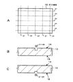
図1A〜Dにおいては、本発明構成によるガラス基板1の模式的な構成を示す。このガラス基板1の材料としては、Na、K及びSiO2 より成るいわゆるソーダガラスの他、無アルカリガラスを用いることもできる。
図1Aに示すように、ガラス基板1は第1の主面1A及び第2の主面1Bを有し、例えば矢印x及びyで示す直交する2方向に沿う第1の側面3A及び第2の側面3Bを有する。
そして本発明によるガラス基板は、図1Bに示すように、第1の側面3Aには、第1の主面1Aからの深さがd1 のレーザ痕2Aが形成され、図1Cに示すように、第2の側面3Bには、第1の主面1Aからの深さd2 のレーザ痕2Bが形成され、上記各深さd1 とd2 が、d1 ≠d2 とされてなる。
また他の本発明によるガラス基板は、図1Bに示すように第1の側面3Aに第1の主面からの深さがd1 とされたレーザ痕2Aが形成され、図1Dに示すように、第2の側面3Bには、第2の主面1Bからの深さがd2 のレーザ痕2Bが形成されてなる。この場合は、深さd1 及びd2 はd1 =d2 としても、d1 ≠d2 としてもよい。
【0021】
次にこのようなガラスの切断方法について説明する。
先ず、図2Aに模式的な平面図を示すように、厚さ例えば0.7mmのソーダガラス等より成るガラス原板10に対し、図2Aにおいて破線x1〜x5で示す第1の切断方向と、図2Aにおいて破線y1〜y5で示す第2の切断方向にレーザ光の照射及び強制冷却による切断を行う。
【0022】
本発明においては、図2B及びCにおいてそれぞれガラス原板10の第1の主面1A上の切り欠き凹部としてレーザ光の照射領域を示すように、第1及び第2の切断方向におけるレーザ照射部の切断深さを異ならしめる。
即ち、図2Aにおける破線x1 〜x5 に対応する第1の切断方向においては、図2Bに示すように、矢印x1'〜x5'で示す図2Bの紙面に垂直な方向にレーザ光を走査照射するにあたって、第1の切断方向の深さをd1 とする。
そして、図2Aにおける破線y1 〜y5 に対応する第2の切断方向においては、図2Cに示すように、矢印y1'〜y5'で示す図2Cの紙面に垂直な方向にレーザ光を走査照射するにあたって、この第2の切断方向の深さd2 を上記d1 とは異なる深さとなるようにレーザ光の照射を行う。
【0023】
この各切断方向における深さを異ならしめる具体的な方法としては、照射するレーザ光のレーザパワー又は送り速度を異ならしめる方法を採ることができる。
レーザ光照射の条件変化による加工深さの定量的な測定は、これまで定義そのものが統一されておらず、数値化することは一般的に行われていないが、簡単のため、本明細書においては単位面積当たりに照射するエネルギーとレーザ加工深さとが比例するとして後述する実施例及び比較例を行った。
【0024】
また、他の本発明においては、図3A〜Cにおいて模式的に示すように、レーザ光の照射をガラス原板10の第1の主面1A側と、第2の主面1B側とからそれぞれ行う。
即ち、図3Aにおいて破線x1 〜x5 で示す第1の切断方向の切断は、図3Bに模式的に矢印x1'〜x5'で示すように、図3Aの紙面に垂直な方向にレーザ光を走査照射するにあたって、ガラス原板10の第1の主面1A上にレーザ光を照射して切断を行う。
そして、図3Aにおいて破線y1 〜y5 で示す第2の切断方向の切断は、図3Cに模式的に矢印y1'〜y5'で示すように、図3Cの紙面に垂直な方向にレーザ光を走査照射するにあたって、ガラス原板10の第2の主面1B上からレーザ光の照射を行って切断する。
【0025】
尚、上述の図2B、C及び図3B、Cにおいて、レーザ光を照射する領域において切り欠き凹部として切断部を模式的に示したが、この切断部は、図1A〜Dにおいて説明した切断側面におけるレーザ痕2を構成する領域を模式的に表すものであり、レーザ照射及び強制冷却によって、この切り欠き凹部に相当する主面直下にレーザ痕が形成され、その下部に基板の主面に垂直な切断側面が形成される。
【0026】
また、上述のいずれの場合においても、レーザ光を走査照射した直後に、例えばエタノール、メタノール、イソプロピルアルコール、アセトン等の揮発性物質や、空気又はN2 ガス等の圧縮ガスを噴出するノズルをレーザ光スポットに近接させて走査させ、レーザ光照射直後に強制冷却を行うようにする。
【0027】
【実施例】
次に、上述の本発明によるガラスの切断方法によって、以下の実施例1〜10、比較例1〜5で示すガラス基板の切断を行い、本発明による寸法精度の有意な効果を確認した。
以下の実施例及び比較例においては、厚さ0.7mmのソーダガラスより成るガラス原板10を用意し、これに対し、レーザパワー50Wの炭酸ガスレーザの照射及びエタノールのノズルからの噴射による強制冷却を行って、目標寸法として横87.65mm、縦64.65mmのタッチパネル用のガラス基板の切断を行った。
上述の図2Aにおいて破線x1 〜x5 で示す第1の切断方向において、炭酸ガスレーザのレーザ送り速度を4.8m/分として走査照射し、また上述の図2Aにおいて破線y1 〜y5 で示す第2の切断方向において、炭酸ガスレーザのレーザ送り速度を5.2m/分として走査照射してそれぞれ実施例1〜5のガラス基板の切断を行った。
【0028】
これら実施例1〜5における各ガラス基板の上下両端部での横寸法を横寸法1、2とし、また左右両端部での縦寸法を縦寸法1、2として下記の表1に記載した。寸法単位は全てmmである。
【0029】
【表1】

また、比較例1〜5として、同様の材料構成のガラス原板から、上記実施例1〜5と同様の目標寸法のガラス基板を、レーザ送り速度は4.8m/分として固定して切断を行った。この結果を下記の表2に示す。
【0031】
【表2】
この結果から、本発明によるガラスの切断方法、即ち第1及び第2の切断方向においてレーザ光の送り速度を異ならしめる方法による実施例1〜5においては、その切断後の寸法形状を、目標とする寸法に対しプラス誤差で最大で0.15mm、マイナス誤差は0.00mmに抑えて形成することができた。
これに対し、レーザ光の送り速度を同一とする比較例1〜5においては、プラス誤差で最大0.3mm、マイナス誤差では−0.31mmと寸法形状のばらつきを生じることがわかった。また、比較例1〜5において、各切断側面において目視にてバリが生じていることを確認した。
【0033】
尚、上述のレーザ光の送り速度を4.8m/分から4%未満の変化量となる4.9m/分として変化させ、第1及び第2の切断側面を形成したところ、有意な結果を得ることができず、上述の比較例1〜5と同様に、誤差幅0.3mm程度の寸法精度しか得ることができなかった。また、目視にて切断側面にバリが生じていることが確認された。これに対し、逆り速度を4%以上変化させる例えば5.0m/分とするとき、表1に示す例と同様の誤差幅が得られた。また、切断面にバリは認められなかった。
【0034】
また、レーザ光のレーザパワーを異ならしめる場合についての考察も行った。第1の切断方向においてレーザパワー50W、第2の切断方向においてレーザパワー48Wとして上述の実施例1〜5と同様の材料構成をもってガラス基板の切断を行ったところ、上述の各実施例と同様に、誤差幅0.15mm程度の寸法精度をもってガラス基板を切断することできた。
【0035】
更にこの場合においても、レーザパワーの変化量を4%未満として第1及び第2の切断方向においてレーザの照射及び強制冷却を行ってガラスの切断を行ったところ、上述の各比較例と同様に、誤差幅が0.3mm程度以上となり、しかも目視にてバリが生じていることが確認された。
【0036】
従って、本発明においては、レーザ痕の深さを異ならしめる具体的な方法として、レーザ光の送り速度及びレーザパワーを4%以上異ならしめて照射するものとする。
【0037】
また、レーザ痕の深さとしては、以下の測定結果から、0.06mm以上の深さが必要であることがわかった。
以下の例においては、厚さ0.7mm及び0.55mmのソーダガラスより成るガラス原板を用意した。上述の第1及び第2の切断方向において、レーザ痕の深さを異ならしめて、浅い方のレーザ痕の深さと、各切断後のガラス基板に対する静荷重強度を測定した。静荷重強度は、通常のガラス破壊強度測定装置により測定した加圧子の直径は20mm、加圧速度は1mm/秒とした。この結果を、以下の表3に示す。
【0038】
【表3】
この結果からわかるように、レーザ痕の深さが0.06mm未満の0.04mmの場合は、静荷重強度が28kgf以下と格段に劣ることがわかる。これに対し、レーザ痕の深さを0.06mmとした場合は、レーザ痕深さが0.04mmの場合と比較して、静荷重強度が厚さ0.7mmのガラスで21kgf、厚さ0.55mmのガラスで12kgfも強度が増加している。
従って、本発明によるガラス基板においては、そのレーザ痕の深さを0.6mm以上に選定するものである。
【0040】
次に、レーザ照射によって、第1の切断方向と第2の切断方向とにおいて、ガラス原板の第1及び第2の主面から切断を行う場合について測定した結果を示す。
実施例6〜10においては、第1の主面と第2の主面からレーザパワー50W、レーザ送り速度を4.8m/分としてレーザ光の照射及び強制冷却による切断を行い、切断された各ガラス基板の寸法精度を上述の実施例1〜5及び比較例1〜と5と同様に測定した。表4において寸法単位はmmである。
【0041】
【表4】
この結果からわかるように、第1及び第2の主面からレーザ光を照射する場合には、寸法誤差がプラス誤差で0.05mm、マイナス誤差で0.00mmであり、誤差幅を0.05mm以下に抑制できることがわかる。
【0043】
また、上述の各実施例1〜10における切断側面の表面粗さをAFM(Atomic Force Microscope;原子間力電子顕微鏡)により測定したところ、全ての実施例において、表面粗さは50nm以下に抑制できることがわかった。
【0044】
更に、これらの実施例を含め、本発明により切断したガラス基板と、超硬ローラーカットにより切断したガラス基板との静荷重強度を測定した結果を図4に示す。この場合においても静荷重強度は、通常のガラス強度測定装置により測定した。加圧子の直径は20mm、加圧速度は1mm/秒とした。図4において、実線aは本発明によるガラス基板、実線bは超硬ローラー切断による従来構成のガラス基板である。サンプル数のピークは、本発明では65kgf程度の静荷重強度であり、従来構成のガラス基板では30kgf程度の強度しか得られていない。
【0045】
この結果から、本発明のガラス切断方法により切断したガラス基板は、ほぼ45kgf程度以上の静荷重強度を有することがわかる。
【0046】
このような従来に比し強度特性に優れたガラス基板をタッチパネルに適用した例を図5A及びBに模式的に示す。図5Aにおいては、タッチパネルに適用したガラス基板を載置固定するフレーム21を示す。フレーム21はAl合金等より成り、液晶型表示装置、有機EL(Electro Luminescence)型表示装置等の各種表示体上に固定配置され、表示面に対応する位置に窓抜部22が形成されて成る。
【0047】
図5Bに、このフレーム21上にタッチパネル30を固定載置した状態の模式的な断面構成を示す。タッチパネル30は、ガラス基板1上に、図示しないがITO(In−Snの複合酸化物)等より成る光透過性の導電層が所定のパターンにスパッタリング等により形成されて成り、この上に、アクリル樹脂等より成るスペーサを介して、内側にITO等の光透過性の導電層がパターン形成されたフィルム基材31がガラス基板1と所定の間隔をもって対向配置され、例えば外縁部32において、例えば粘着テープ等により、数μm程度の間隔をもって支持及び固定されて構成される。
【0048】
本発明においては、ガラス基板1の強度を高めると共に、特にこのフレーム21の窓抜部内端縁部23を、図6A〜Cに模式的に示すように、各種加工を施した形状として構成する。例えば、図6Aに示すように、半径rが0.2mm以上0.5mm以下の周面部23a、いわゆるR面を設ける。
または、図6Bに示すように、内端縁部からの長さlが0.2mm以上0.5mm以下、ガラス基板と平行な面からの角度θが10°以上45°以下の斜面部23bを設ける。
更にまたは、図6Cに示すように、内端縁部からの幅wが0.2mm以上0.5mm以下、ガラス基板と対向する面からの段差高hが0.2mm以上0.5mm以下の段差部23cを設ける。
【0049】
このように窓抜部内端縁部23を加工することによって、このフレーム21上にテープ、糊等によって固着されるガラス基材の耐荷重強度を増大化することができた。
【0050】
尚、上述のフレーム21の窓抜部内端縁部23に周面部を形成する場合は、半径rを0.2mm未満とすると著しく歩留りが低下し、また0.5mmを越える場合はガラス割れに対して有効であるが、製造工程において作業性の低下を来す。従って、周面部を構成する場合は、半径rを0.2mm〜0.5mmの範囲とすることが望ましい。
また、窓抜部内端縁部23に斜面部を形成する場合、0.2mmの長さlで角度θが45°以上になると、歩留りの変化が見られない。長さlが0.2mm〜0.5mmの範囲で角度θを10〜45°とするときに、安定した強度が得られることから、斜面部を構成するときは、上述の範囲に選定することが望ましい。
更に、段差部を設ける場合においても、上述したように段差幅wを0.2mm〜0.5mm、段差高hを0.2mm〜0.5mmの範囲に選定する場合に、ガラス強度に有意な効果を得ることができた。従って、段差部の形状は上述の範囲に選定することが望ましい。
【0051】
このように、タッチパネルを固定配置する表示体上のフレームの窓抜部内端縁部に周面部、斜面部または段差部を形成することによって、更にガラスの耐荷重強度を高めることができ、製品の強度の向上を高めることができる。
【0052】
尚、ガラス基板の材料としては、上述したようにソーダガラス等を用いることができるが、フロート法により製造されたガラス基板を用いる場合は、以下の方法により更に強度を保持することができる。
フロート法とは、溶融Sn上にガラス材料を板状に溶かし流して、溶融Snとは接していない側の表面に圧縮応力を生じさせてこの面の平坦度を向上させるガラスの製造方法である。このフロート法により製造されたガラス基板は、図7Aに模式的に示すように、フロート面側(溶融Snと接していた面)とは反対側の面において圧縮応力p1 及びp2 が生じる。ここに、フロート面3側から矢印g1 で示すように荷重を負荷すると、圧縮応力p1 及びp2 を相殺する方向に張力が生じる。
【0053】
図7Bに示すように、負荷荷重g2 が小さい場合は張力t1 及びt2 を圧縮応力p1 及びp2 で相殺し、図7Cに示すように、負荷荷重g3 が大きくなると、張力t1 ’及びt2 ’と圧縮応力p1 及びp2 がつりあう。ガラス基板1は通常この状態まで耐荷重強度が保持される。更に負荷荷重が大きくなると、図7Dに示すようにガラス基板1は破壊される。
【0054】
このように、フロート法によって製造されたガラス基板は、表面に圧縮応力を有することから、その裏面からの耐荷重強度が他のガラス基板に比して高い。
しかしながら、このガラス基板1をタッチパネルのガラス基板に適用する場合、光透過性導電層、SiO2 被膜等をスパッタリング法、蒸着法、ディップ法などにより成膜する場合にガラス基板が300℃以上の高温に加熱される。
【0055】
このとき、フロート法によって製造されたガラス基板の持つ圧縮応力が熱によって開放されてしまうアニール効果により、本来の耐荷重強度を保持することができなくなってしまう。つまり、上述の図7A〜Cにおいて説明した圧縮応力に起因する強度が消失してしまうこととなる。これにより、フロート面3からの耐荷重強度が劣化してしまう。
【0056】
本発明者等は、上述のスパッタリング法或いは蒸着法によりITO等の導電層を成膜する際に、200℃以下の低温成膜法を用いることによって、応力の熱による開放を低減化させることができ、成膜後の耐荷重強度において有意な差を得ることができた。
【0057】
以下の表5は、従来のスパッタリングによる成膜後のガラス基板と、低温スパッタリングによる成膜後のガラス基板とのサンプル数、平均耐荷重強度(N)、その標準偏差、最小値及び最大値を示したものである。
【0058】
【表5】
この表5らわかるように、従来による成膜後のガラス基板は、平均値でおよそ9N耐荷重が劣化するのに対し、200℃以下の低温スパッタリングによる場合は、およそ2N程度の耐荷重劣化に止まっている。
従って、ガラス基板上に200℃以下の低温スパッタリング法によってITO等の光透過性の導電層を形成することによって、フロート法により製造した場合のガラス基板の本来もつ強度を保持することができ、更に製品の強度を保持することができて、製品の信頼性の向上をはかることができることがわかる。
【0060】
上述したように、本発明によれば、ガラスの切断方法において、第1及び第2の切断方法におけるレーザ光のレーザパワーまたはレーザ光の走査移動速度を変えて切断を行い、切断後のガラス基板の切断側面におけるレーザ痕の深さを異ならしめることによって、切断側面における傾斜面や湾曲面の発生を回避し、垂直な切断側面をもってガラス基板を形成することができる。
【0061】
尚、上述の各例においては、ガラス基板をタッチパネル又は携帯端末上のタッチパネルに適用した場合について説明したが、本発明は、上述の本発明構成を逸脱しない範囲において、種々の変形、変更が可能であることはいうまでもない。例えば、PDA(Personal Digital Assistant)、POS(Point Of Sales)、ATM(Automatic Teller Machine)等種々の表示体に用いられるガラス基板に適用することができる。
【0062】
【発明の効果】
上述したように、ガラスの切断方法において、切断後のガラス基板の切断独面におけるレーザ痕の深さを異ならしめることによって、またガラス基板1の第1及び第2の主面からレーザ痕を形成することによって、ガラス切断側面におけるひび、欠けの発生を回避し、粉砕粉の付着のないガラス基板を所望の寸法精度もって歩留り良く、また生産性良く製造することができる。
【0063】
このようなガラスの切断方法によれば、切断側面においてクラックの発生を抑制し、これに起因するガラス割れの減少と、ガラスの欠けの激減によって、特性に優れたタッチパネル用のガラス基板を提供することができる。
また、ガラスの静荷重強度を従来に比して高い55kgf程度以上に向上させることができ、このガラス基板を用いたタッチパネルにおいて製品の強度の向上をはかることができる。
【0064】
特に、タッチパネル特有の入力時の圧力、また生活上の不可抗力により加わる荷重、衝撃に対する強度を高めることができ、製品故障の低減化、消費者からのクレームの削減をはかることが可能となる。
【0065】
本発明によれば、タッチパネル、携帯端末等における製品自体の信頼性の向上、耐久性及び品質の向上をはかることができ、更にガラス基板の薄型化を可能とし、タッチパネル及び携帯端末の薄型化、小型軽量化をはかることができる。
【0066】
また、小型化をはからない場合に基板の薄型化をはかることによって、省スペース化による機能付加による製品の高機能化も可能となり、また製品組立精度の向上と品質のばらつきの低減化をはかることができる。
【図面の簡単な説明】
【図1】Aはガラス基板の一例の模式的な斜視図である。
Bはガラス基板の一例の模式的な要部側面図である。
Cはガラス基板の一例の模式的な要部側面図である。
Dはガラス基板の一例の模式的な要部側面図である。
【図2】Aはガラスの切断方法の一例の説明図である。
Bはガラスの切断方法の一例の説明図である。
Cはガラスの切断方法の一例の説明図である。
【図3】Aはガラスの切断方法の一例の説明図である。
Bはガラスの切断方法の一例の説明図である。
Cはガラスの切断方法の一例の説明図である。
【図4】ガラス基板の耐荷重強度のサンプル分布を示す図である。
【図5】Aはタッチパネルのフレームの模式的な平面図である。
Bはタッチパネルのフレームの模式的な断面図である。
【図6】Aはタッチパネルのフレームの窓抜部内端縁部の説明図である。
Bはタッチパネルのフレームの窓抜部内端縁部の説明図である。
Cはタッチパネルのフレームの窓抜部内端縁部の説明図である。
【図7】Aはガラス基板の強度の説明図である。
Bはガラス基板の強度の説明図である。
Cはガラス基板の強度の説明図である。
Dはガラス基板の強度の説明図である。
【図8】従来のガラス基板の一例の模式的な断面図である。
【図9】Aはガラス切断方法の説明図である。
Bはガラス切断側面の説明図である。
Cはガラス切断側面の説明図である。
【符号の説明】
1…ガラス基板、1A…第1の主面、1B…第2の主面、2…レーザ痕、2A…レーザ痕、2B…レーザ痕、10…ガラス原板、21…フレーム、22…窓抜部、23…窓抜部内端縁部、23a…周面部、23b…斜面部、23c…段差部、30…タッチパネル、31…フィルム基材、32…外縁部[0001]
BACKGROUND OF THE INVENTION
The present invention particularly relates to a glass substrate for a touch panel which is cut by irradiation with laser light and forced cooling, and a touch panel.as well asMobile phoneThe end of theInvolved.
[0002]
[Prior art]
In general, as a glass cutting method for forming a glass substrate having a predetermined width and length by cutting an original glass plate vertically and horizontally, for example, a mechanical method or a laser as disclosed in JP-A-11-71124 The laser type etc. which irradiate light are used.
[0003]
When a cutting method using mechanical processing is employed, cutting is performed by pressurizing the glass to cause a median crack, that is, a crack extending in a direction perpendicular to the glass surface. In this cutting method, the glass cut surfaces opened in the blade pressure-removing step come into contact with each other, thereby generating a lateral crack, that is, a crack extending in the horizontal direction on the glass surface.
[0004]
For this reason, in the mechanical glass cutting process, it was impossible to completely prevent micro cracks generated on the cut surface, that is, lateral cracks. When cracks or cracks occur, pulverized powder causes so-called cullet, and the cullet adheres to the surface of the display body, impairing visibility, or when a glass substrate is used for a touch panel, etc. This causes inconveniences such as causing a short circuit due to adhesion.
There is a method of reducing such lateral cracks by chemical treatment, but this leads to a decrease in productivity and an increase in cost. In addition, there is a problem that the glass strength varies due to chemical treatment.
[0005]
On the other hand, in the case of using the laser method, for example, a heat cutting method using a carbon dioxide laser is proposed in Japanese Patent Application Laid-Open Nos. 8-217478 and 11-254172.
However, in the case of a cutting method using only ordinary laser light irradiation, as shown in a schematic cross-sectional configuration of an example in FIG. 8, the laser light irradiation side surface of the
[0006]
On the other hand, a method has been proposed in which heat is generated in a glass by a combined action of heating by laser light irradiation such as a carbon dioxide laser and forced cooling using water or compressed air, and cutting is performed as a trigger for glass cutting. ing.
In particular, as a simple input method in recent years, the thickness is 1.1 mm or less, for example, about 0.3 to 0.7 mm, which is used for a touch panel attached to the surface of various display bodies or a portable terminal using the same. At the time of cutting a thin glass substrate, a cutting method using laser light irradiation and forced cooling is drawing attention.
This method is advantageous in that there is almost no generation of microcracks since no mechanical force is applied.
[0007]
[Problems to be solved by the invention]
However, even in the case of performing such laser light irradiation and forced cooling, as schematically shown in FIG.1The horizontal direction indicated by the position of, and the broken line y1And y2When cutting is performed by irradiating the laser beam in the vertical direction and forced cooling as shown in Fig. 9, there is a problem that burrs 11 and chips 12 are generated at the intersection a where the laser beam is irradiated vertically and horizontally as shown in FIG. 9B. It was.
At this intersection a9Although it is desirable that the cut surface be vertical as shown in C, the cut surface is actually inclined or curved, leading to deterioration of dimensional accuracy, lowering of productivity and yield, and cost. The increase of the problem is a problem.
[0008]
In the present invention, when a glass substrate having a predetermined size is cut from a glass original plate, cracks and chips on the cut surface as described above do not occur, so generation of pulverized powder from this portion is avoided, and strength characteristics are further improved. An object is to provide an excellent glass substrate for touch panel, a touch panel and a portable terminal.
[0009]
[Means for Solving the Problems]
The present invention is cut at least by laser light irradiation.For touch panelIt is a glass substrate, the surface roughness of the cut side surface of the glass substrate is 50 nm or less, and the depth of the laser mark on the cut side surface is 0.06 mm or more.The strength by static load test is 55kgf to 90kgfConstitute.
Further, according to the present invention, in the above-described configuration, the depth of the laser mark is different between the first cut side surface of the glass substrate and the second cut side surface different from the first cut side surface.
[0010]
Furthermore, the present invention is configured such that the depth of the above-described laser mark is different by 2% or more on the first and second cut side surfaces.
[0011]
Still further, according to the present invention, in each of the above-described configurations, the laser mark is formed with a predetermined depth from the first main surface of the glass substrate at the first cut side surface of the glass substrate, The second cut side surface is different from the second main surface, which is the back surface of the first main surface, with a predetermined depth.
[0012]
For example,A glass cutting method for performing laser beam irradiation and forced cooling on a glass original plate, wherein a laser is used in a first cutting direction relative to the glass original plate and a second cutting direction different from the first cutting direction. Cutting is performed by changing the laser power or feed rate of light.
Also,UpIn the glass cutting method described above, the laser power or feed rate of the laser light is changed by 4% or more between the first cutting direction and the second cutting direction.
[0013]
FurtherIn addition,A glass cutting method for performing laser beam irradiation and forced cooling on a glass original plate, and cutting the glass original plate in a first cutting direction by irradiating the glass original plate with laser light from a first main surface. Then, cutting in a second cutting direction different from the first cutting direction with respect to the glass original plate is performed by irradiating a laser beam from the second main surface which is the back surface of the first main surface.
[0014]
Furthermore, the present invention is based on the above configuration.For touch panelThe glass substrate is configured to be used for a touch panel in which a light transmissive conductive layer is formed on a glass substrate, and a film base material is disposed opposite to the glass substrate with a predetermined interval.
Furthermore, the present invention is based on the above configuration.For touch panelA glass substrate is used for a portable terminal having a touch panel.
[0015]
As mentioned aboveIn addition,In a glass cutting method in which laser light irradiation and forced cooling are performed, the laser power or the laser light feed speed is set so that the depth of the laser mark is different between the first cut side surface and the second cut side surface of the glass substrate. By irradiating differently and then performing forced cooling immediately after cutting, cracks and burrs can be avoided at the intersection of the first and second cut side surfaces, and the glass substrate can have a desired dimensional accuracy. Could be cut.
[0016]
Further, the cutting in the first cutting direction and the cutting in the second cutting direction of the glass substrate are performed by irradiating laser light from different main surfaces (front surface and back surface) of the glass substrate, respectively, so to speak differently. By separating the laser mark vertically on the side surface and cutting, cracks and burrs can be avoided at the intersection of the first and second cut side surfaces, and the glass substrate can be cut with the desired dimensional accuracy. We were able to.
[0017]
This avoids the generation of strain stress caused by heating by laser light irradiation and subsequent forced cooling in two directions at the intersection of the cut side surfaces, and the vertical direction of glass cutting, that is, the main surface of the glass substrate. This is probably because the stress was generated only in the vertical direction and the cutting was able to be performed.
[0018]
like thisNaAccording to the lath cutting method, the surface roughness of the cut side surface is 50 nm or less, a glass substrate that does not require chemical treatment of the side surface can be obtained, and the strength by the static load measurement is maintained at 55 kgf or more. I was able to.
OnlyAlso,A thin glass substrate with desired dimensional accuracy can be manufactured with good productivity and yield without cracks and burrs. When the glass substrate according to the present invention is used for a touch panel or a portable terminal, productivity and yield can be improved. Improvements and cost reductions can be achieved.
[0019]
DETAILED DESCRIPTION OF THE INVENTION
Hereinafter, embodiments of a glass substrate and a glass cutting method according to the present invention, and examples and comparative examples based thereon will be described in detail with reference to the drawings. In the following example, a case where the present invention is applied to a glass substrate of a portable terminal equipped with a touch panel and a cutting method thereof will be described. However, the present invention can be variously modified and changed without departing from the configuration of the present invention. Needless to say.
[0020]
1A to 1D show a schematic configuration of a
As shown in FIG. 1A, the
In the glass substrate according to the present invention, as shown in FIG. 1B, the first side surface 3A has a depth d from the first main surface 1A.1The
In another glass substrate according to the present invention, the depth from the first main surface is d on the first side surface 3A as shown in FIG. 1B.1As shown in FIG. 1D, the second side surface 3B has a depth d from the second main surface 1B.2The laser mark 2B is formed. In this case, the depth d1And d2D1= D2As well as d1≠ d2It is good.
[0021]
Next, a method for cutting such glass will be described.
First, as shown in a schematic plan view in FIG. 2A, a glass
[0022]
In the present invention, the laser irradiation portions in the first and second cutting directions are shown in FIGS. 2B and 2C so as to show the irradiation regions of the laser light as cutout recesses on the first
That is, the broken line x in FIG.1~ XFiveIn the first cutting direction corresponding to, as shown in FIG.1'~ XFiveWhen the laser beam is scanned and irradiated in the direction perpendicular to the paper surface of FIG. 2B indicated by ', the depth in the first cutting direction is d1And
And the broken line y in FIG. 2A1~ YFiveIn the second cutting direction corresponding to, as shown in FIG.1'~ YFiveWhen the laser beam is scanned and irradiated in the direction perpendicular to the paper surface of FIG.2The above d1Irradiation with a laser beam is performed so that the depth is different from that of.
[0023]
As a specific method of varying the depth in each cutting direction, a method of varying the laser power or feed rate of the laser beam to be irradiated can be employed.
Quantitative measurement of processing depth due to changes in laser light irradiation conditions has not been standardized so far, and it has not been generally quantified. The examples and comparative examples to be described later were performed assuming that the energy irradiated per unit area is proportional to the laser processing depth.
[0024]
In another embodiment of the present invention, as schematically shown in FIGS. 3A to 3C, laser light irradiation is performed from the first
That is, the broken line x in FIG.1~ XFiveThe cutting in the first cutting direction indicated by is schematically shown in FIG.1'~ XFiveAs indicated by ', when the laser beam is scanned and irradiated in the direction perpendicular to the paper surface of FIG. 3A, the first
And the broken line y in FIG. 3A1~ YFiveThe cutting in the second cutting direction indicated by is schematically shown in FIG.1'~ YFiveAs indicated by ', when the laser beam is scanned and irradiated in the direction perpendicular to the paper surface of FIG. 3C, the laser beam is irradiated from the second
[0025]
In FIGS. 2B and 2C and FIGS. 3B and 3C, the cut portion is schematically shown as a notch recess in the region irradiated with laser light. This cut portion is the cut side surface described in FIGS. The region constituting the laser mark 2 is schematically represented by laser irradiation and forced cooling, whereby a laser mark is formed immediately below the main surface corresponding to the notch recess and perpendicular to the main surface of the substrate. A cut side surface is formed.
[0026]
In any of the above cases, immediately after scanning with laser light, volatile substances such as ethanol, methanol, isopropyl alcohol, and acetone, air, or N2A nozzle that ejects a compressed gas such as a gas is scanned close to the laser beam spot, and forced cooling is performed immediately after laser beam irradiation.
[0027]
【Example】
Next, the glass substrate shown by the following Examples 1-10 and Comparative Examples 1-5 was cut | disconnected by the glass cutting method by the above-mentioned this invention, and the significant effect of the dimensional accuracy by this invention was confirmed.
In the following examples and comparative examples, a glass
Broken line x in FIG. 2A above1~ XFiveIn the first cutting direction shown in FIG. 2A, scanning irradiation is performed with the laser feed rate of the carbon dioxide laser set to 4.8 m / min.1~ YFiveIn the second cutting direction, the glass substrates of Examples 1 to 5 were cut by scanning irradiation with a carbon dioxide laser feed rate of 5.2 m / min.
[0028]
The horizontal dimensions at the upper and lower ends of each glass substrate in Examples 1 to 5 are set as
[0029]
[Table 1]
Further, as Comparative Examples 1 to 5, a glass substrate having the same target size as that of Examples 1 to 5 was fixed and cut at a laser feed rate of 4.8 m / min from a glass original plate having the same material structure. It was. The results are shown in Table 2 below.
[0031]
[Table 2]
From this result, in Examples 1 to 5 according to the glass cutting method according to the present invention, that is, the method of varying the laser beam feeding speed in the first and second cutting directions, the dimension and shape after the cutting are targeted. For the dimension toWith plus error0.15m at maximumm,The minus error was able to be formed with a limit of 0.00 mm.
On the other hand, in Comparative Examples 1 to 5 in which the feeding speed of the laser beam is the same, it was found that the variation in size and shape is 0.3 mm at the maximum with a plus error and -0.31 mm with a minus error. Moreover, in Comparative Examples 1-5, it confirmed that the burr | flash produced visually at each cut side.
[0033]
In addition, when the feed rate of the laser beam is changed from 4.8 m / min to 4.9 m / min, which is less than 4%, and the first and second cut side surfaces are formed, a significant result is obtained. As in Comparative Examples 1 to 5 described above, only dimensional accuracy with an error width of about 0.3 mm could be obtained. Moreover, it was confirmed visually that burrs were generated on the cut side surface. On the other hand, when the reverse speed was changed by 4% or more, for example, 5.0 m / min, the same error width as the example shown in Table 1 was obtained. Further, no burrs were observed on the cut surface.
[0034]
In addition, consideration was given to the case where the laser power of the laser light is made different. When the glass substrate was cut with the same material structure as in Examples 1 to 5 described above with a laser power of 50 W in the first cutting direction and a laser power of 48 W in the second cutting direction, the same as in each of the above examples. The glass substrate could be cut with a dimensional accuracy of an error width of about 0.15 mm.
[0035]
Further in this case, the amount of change in laser power was set to less than 4%, and the glass was cut by performing laser irradiation and forced cooling in the first and second cutting directions, as in the above comparative examples. The error width was about 0.3 mm or more, and it was confirmed that burrs were generated visually.
[0036]
Therefore, in the present invention, as a specific method for making the depth of the laser mark different, the laser beam feed speed and the laser power are made different by 4% or more for irradiation.
[0037]
Moreover, as the depth of the laser mark, it was found from the following measurement results that a depth of 0.06 mm or more is necessary.
In the following example, a glass original plate made of soda glass having a thickness of 0.7 mm and 0.55 mm was prepared. In the first and second cutting directions described above, the depth of the laser mark was varied, and the depth of the shallow laser mark and the static load strength on the glass substrate after each cutting were measured. As for the static load strength, the diameter of the pressurizer measured by a normal glass breaking strength measuring device was 20 mm, and the pressurization speed was 1 mm / second. The results are shown in Table 3 below.
[0038]
[Table 3]
As can be seen from this result, when the depth of the laser mark is 0.04 mm which is less than 0.06 mm, the static load strength is 28 kgf or less, which is remarkably inferior. On the other hand, when the depth of the laser mark is 0.06 mm, compared with the case where the laser mark depth is 0.04 mm, the static load strength is 21 kgf with a thickness of 0.7 mm and a thickness of 0 mm. The strength is increased by 12 kgf with .55 mm glass.
Therefore, in the glass substrate according to the present invention, the depth of the laser mark is selected to be 0.6 mm or more.
[0040]
Next, the result measured about the case where it cuts from the 1st and 2nd main surface of a glass original plate in a 1st cutting direction and a 2nd cutting direction by laser irradiation is shown.
In Examples 6 to 10, each of the first main surface and the second main surface was cut by laser light irradiation and forced cooling with a laser power of 50 W and a laser feed rate of 4.8 m / min. The dimensional accuracy of the glass substrate was measured in the same manner as in Examples 1 to 5 and Comparative Examples 1 and 5 described above. In Table 4, the dimensional unit is mm.
[0041]
[Table 4]
As can be seen from this result, when laser light is irradiated from the first and second main surfaces, the dimensional error is 0.05 mm as a plus error, 0.00 mm as a minus error, and the error width is 0.05 mm. It turns out that it can suppress below.
[0043]
Moreover, when the surface roughness of the cut side surface in each of the above-described Examples 1 to 10 was measured with an AFM (Atomic Force Microscope), the surface roughness can be suppressed to 50 nm or less in all the Examples. I understood.
[0044]
Furthermore, the result of having measured the static load strength of the glass substrate cut | disconnected by this invention including these Examples and the glass substrate cut | disconnected by the cemented carbide roller cut is shown in FIG. Even in this case, the static load strength isStrengthMeasured with a degree measuring device. The diameter of the pressurizer was 20 mm, and the pressurization speed was 1 mm / second. In FIG. 4, a solid line a is a glass substrate according to the present invention, and a solid line b is a glass substrate having a conventional configuration obtained by cutting a carbide roller. The peak of the number of samples is a static load strength of about 65 kgf in the present invention, and only a strength of about 30 kgf is obtained with a glass substrate having a conventional configuration.
[0045]
From this result, the glass substrate cut by the glass cutting method of the present invention is almost4It can be seen that it has a static load strength of about 5 kgf or more.
[0046]
FIGS. 5A and 5B schematically show an example in which such a glass substrate having excellent strength characteristics as compared with the conventional case is applied to a touch panel. In FIG. 5A, the flame |
[0047]
FIG. 5B shows a schematic cross-sectional configuration in a state where the
[0048]
In the present invention, the strength of the
Alternatively, as shown in FIG. 6B, a slope portion 23b having a length l from the inner edge of 0.2 mm to 0.5 mm and an angle θ from a plane parallel to the glass substrate of 10 ° to 45 °. Provide.
Furthermore, as shown in FIG. 6C, a step w having a width w from the inner edge of 0.2 mm to 0.5 mm and a step height h from the surface facing the glass substrate of 0.2 mm to 0.5 mm. A portion 23c is provided.
[0049]
By processing the
[0050]
In the case where the peripheral surface portion is formed at the
Further, when the slope portion is formed on the
Further, even when the step portion is provided, as described above, when the step width w is selected within the range of 0.2 mm to 0.5 mm and the step height h within the range of 0.2 mm to 0.5 mm, the glass strength is significant. The effect was able to be acquired. Therefore, it is desirable to select the shape of the stepped portion within the above range.
[0051]
In this way, by forming the peripheral surface portion, the slope portion or the step portion on the inner edge of the window extraction portion of the frame on the display body on which the touch panel is fixedly arranged, the load bearing strength of the glass can be further increased. Strength improvement can be enhanced.
[0052]
As a material for the glass substrate, soda glass or the like can be used as described above. However, when a glass substrate manufactured by the float process is used, the strength can be further maintained by the following method.
The float method is a glass manufacturing method in which a glass material is melted and flowed on molten Sn in a plate shape to generate a compressive stress on the surface not in contact with molten Sn, thereby improving the flatness of this surface. . As schematically shown in FIG. 7A, the glass substrate manufactured by this float process has a compressive stress p on the surface opposite to the float surface (the surface in contact with molten Sn).1And p2Occurs. Here, arrow g from the float surface 3 side1When a load is applied as shown by, the compressive stress p1And p2Tension is generated in the direction that cancels out.
[0053]
As shown in FIG.2When the tension is small, the tension t1And t2Compressive stress p1And p2As shown in FIG.ThreeIncreases, the tension t1'And t2′ And compressive stress p1And p2Balance. The
[0054]
Thus, since the glass substrate manufactured by the float process has a compressive stress on the surface, the load bearing strength from the back surface is high compared with another glass substrate.
However, when this
[0055]
At this time, the original load-bearing strength cannot be maintained due to the annealing effect in which the compressive stress of the glass substrate manufactured by the float process is released by heat. That is, the strength resulting from the compressive stress described in FIGS. Thereby, the load bearing strength from the float surface 3 will deteriorate.
[0056]
The inventors can reduce the release of stress due to heat by using a low-temperature film formation method of 200 ° C. or lower when forming a conductive layer such as ITO by the above-described sputtering method or vapor deposition method. It was possible to obtain a significant difference in the load bearing strength after film formation.
[0057]
Table 5 below shows the number of samples, the average load bearing strength (N), the standard deviation, the minimum value, and the maximum value of the glass substrate after film formation by conventional sputtering and the glass substrate after film formation by low-temperature sputtering. It is shown.
[0058]
[Table 5]
As can be seen from Table 5, the conventional glass substrate after film formation deteriorates with an average value of about 9N load, whereas the low temperature sputtering at 200 ° C. or lower reduces the load resistance to about 2N. At rest.
Therefore, by forming a light-transmitting conductive layer such as ITO on the glass substrate by a low temperature sputtering method of 200 ° C. or less, the original strength of the glass substrate when manufactured by the float method can be maintained, It can be seen that the strength of the product can be maintained and the reliability of the product can be improved.
[0060]
As described above, according to the present invention, in the glass cutting method, cutting is performed by changing the laser power of the laser light or the scanning movement speed of the laser light in the first and second cutting methods, and the glass substrate after cutting. By making the depths of the laser marks on the cut side surfaces different, it is possible to avoid the generation of inclined surfaces and curved surfaces on the cut side surfaces, and to form the glass substrate with the vertical cut side surfaces.
[0061]
In each of the above-described examples, the case where the glass substrate is applied to a touch panel or a touch panel on a mobile terminal has been described. However, the present invention can be variously modified and changed without departing from the above-described configuration of the present invention. Needless to say. For example, the present invention can be applied to glass substrates used for various display bodies such as PDA (Personal Digital Assistant), POS (Point Of Sales), ATM (Automatic Teller Machine).
[0062]
【The invention's effect】
As mentioned above,In the lath cutting method, the glass traces are made different from each other by changing the depth of the laser traces on the cut surface of the glass substrate after cutting, and by forming laser traces from the first and second main surfaces of the
[0063]
like thisGlass cutting methodAccording to the present invention, it is possible to provide a glass substrate for a touch panel having excellent characteristics by suppressing the occurrence of cracks on the cut side surface, and reducing the number of glass cracks resulting from this and reducing the number of glass chips.
Further, the static load strength of the glass can be improved to about 55 kgf or higher, which is higher than the conventional one, and the strength of the product can be improved in the touch panel using the glass substrate.
[0064]
In particular, the pressure at the time of input specific to the touch panel, the load applied by the force majeure in daily life, and the strength against impact can be increased, and it becomes possible to reduce product failures and reduce complaints from consumers.
[0065]
BookAccording to the invention, it is possible to improve the reliability, durability and quality of the product itself in a touch panel, a portable terminal, etc., and further reduce the thickness of the glass substrate, and make the touch panel and the portable terminal thinner and smaller. The weight can be reduced.
[0066]
In addition, by reducing the thickness of the board when not miniaturized, it is possible to increase the functionality of products by adding functions by saving space, and to improve product assembly accuracy and reduce variation in quality. be able to.
[Brief description of the drawings]
FIG. 1A is a schematic perspective view of an example of a glass substrate.
B is a schematic side view of an example of a glass substrate.
C is a schematic side view of an example of a glass substrate.
D is a typical principal part side view of an example of a glass substrate.
FIG. 2A is an explanatory diagram of an example of a glass cutting method.
B is explanatory drawing of an example of the cutting method of glass.
C is explanatory drawing of an example of the cutting method of glass.
FIG. 3A is an explanatory diagram of an example of a method for cutting glass.
B is explanatory drawing of an example of the cutting method of glass.
C is explanatory drawing of an example of the cutting method of glass.
FIG. 4 is a diagram showing a sample distribution of load bearing strength of a glass substrate.
FIG. 5A is a schematic plan view of a touch panel frame.
B is a schematic cross-sectional view of the frame of the touch panel.
FIG. 6A is an explanatory diagram of an inner edge of a window extraction part of a touch panel frame.
B is explanatory drawing of the window edge part inner edge part of the flame | frame of a touchscreen.
C is explanatory drawing of the inner edge part of the window extraction part of the flame | frame of a touchscreen.
FIG. 7A is an explanatory diagram of the strength of a glass substrate.
B is an explanatory view of the strength of the glass substrate.
C is an explanatory view of the strength of the glass substrate.
D is an explanatory view of the strength of the glass substrate.
FIG. 8 is a schematic cross-sectional view of an example of a conventional glass substrate.
FIG. 9A is an explanatory diagram of a glass cutting method.
B is explanatory drawing of the glass cutting | disconnection side surface.
C is an explanatory view of a glass cutting side surface.
[Explanation of symbols]
DESCRIPTION OF
Claims (8)
上記ガラス基板の切断側面の表面粗さが50nm以下であり、
上記切断側面のレーザ痕の深さが0.06mm以上であって、
上記ガラス基板は、静荷重試験による強度が55kgf以上90kgf以下である
ことを特徴とするタッチパネル用のガラス基板。A glass substrate for a touch panel that is cut at least by irradiation with laser light,
The surface roughness of the cut side surface of the glass substrate is 50 nm or less,
The depth of the laser mark on the cut side is 0.06 mm or more,
The glass substrate has a strength by a static load test of 55 kgf or more and 90 kgf or less. A glass substrate for a touch panel.
上記ガラス基板は、少なくともレーザ光の照射により切断されて成り、
上記ガラス基板の切断側面の表面粗さが50nm以下であり、
上記切断側面のレーザ痕の深さが0.06mm以上であって、
上記ガラス基板は、静荷重試験による強度が55kgf以上90kgf以下である
ことを特徴とするタッチパネル。A light-transmissive conductive layer is formed on a glass substrate, and the glass substrate is a touch panel in which a film base material is disposed oppositely with a predetermined interval,
The glass substrate is cut at least by irradiation with laser light,
The surface roughness of the cut side surface of the glass substrate is 50 nm or less,
The depth of the laser mark on the cut side is 0.06 mm or more,
The glass substrate has a strength by a static load test of 55 kgf to 90 kgf.
上記ガラス基板は、少なくともレーザ光の照射により切断されて成り、
上記ガラス基板の切断側面の表面粗さが50nm以下であり、
上記切断側面のレーザ痕の深さが0.06mm以上であって、
上記ガラス基板は、静荷重試験による強度が55kgf以上90kgf以下である
ことを特徴とする携帯端末。A light-transmitting conductive layer is formed on a glass substrate, and the glass substrate is a portable terminal having a touch panel in which a film base is disposed opposite to the glass substrate with a predetermined interval.
The glass substrate is cut at least by irradiation with laser light,
The surface roughness of the cut side surface of the glass substrate is 50 nm or less,
The depth of the laser mark on the cut side is 0.06 mm or more,
The said glass substrate is 55 kgf or more and 90 kgf or less the intensity | strength by a static load test. The portable terminal characterized by the above-mentioned.
Priority Applications (5)
| Application Number | Priority Date | Filing Date | Title |
|---|---|---|---|
| JP2002215760A JP4032857B2 (en) | 2002-07-24 | 2002-07-24 | Glass substrate for touch panel, touch panel and portable terminal |
| US10/621,714 US7479319B2 (en) | 2002-07-24 | 2003-07-18 | Glass substrate and glass cutting method |
| TW092119830A TWI245702B (en) | 2002-07-24 | 2003-07-21 | Glass substrate and glass cutting method |
| KR1020030050127A KR100995939B1 (en) | 2002-07-24 | 2003-07-22 | Glass substrate and glass cutting method |
| CNB031328792A CN1304312C (en) | 2002-07-24 | 2003-07-24 | Glass substrate and glass cutting method |
Applications Claiming Priority (1)
| Application Number | Priority Date | Filing Date | Title |
|---|---|---|---|
| JP2002215760A JP4032857B2 (en) | 2002-07-24 | 2002-07-24 | Glass substrate for touch panel, touch panel and portable terminal |
Publications (2)
| Publication Number | Publication Date |
|---|---|
| JP2004059328A JP2004059328A (en) | 2004-02-26 |
| JP4032857B2 true JP4032857B2 (en) | 2008-01-16 |
Family
ID=31937713
Family Applications (1)
| Application Number | Title | Priority Date | Filing Date |
|---|---|---|---|
| JP2002215760A Expired - Lifetime JP4032857B2 (en) | 2002-07-24 | 2002-07-24 | Glass substrate for touch panel, touch panel and portable terminal |
Country Status (5)
| Country | Link |
|---|---|
| US (1) | US7479319B2 (en) |
| JP (1) | JP4032857B2 (en) |
| KR (1) | KR100995939B1 (en) |
| CN (1) | CN1304312C (en) |
| TW (1) | TWI245702B (en) |
Families Citing this family (24)
| Publication number | Priority date | Publication date | Assignee | Title |
|---|---|---|---|---|
| JP2005247603A (en) * | 2004-03-02 | 2005-09-15 | Okamoto Glass Co Ltd | Method for processing glass article or crystallized glass article and method for producing the article |
| CN101065137A (en) * | 2004-09-16 | 2007-10-31 | 加利福尼亚大学董事会 | G-type peptides and other agents to ameliorate atherosclerosis and other pathologies |
| JP5467705B2 (en) * | 2006-03-24 | 2014-04-09 | Hoya株式会社 | Manufacturing method of glass substrate for magnetic disk and manufacturing method of magnetic disk |
| US8168514B2 (en) * | 2006-08-24 | 2012-05-01 | Corning Incorporated | Laser separation of thin laminated glass substrates for flexible display applications |
| TWI424972B (en) * | 2007-03-02 | 2014-02-01 | Nippon Electric Glass Co | Reinforced plate glass |
| KR100889949B1 (en) * | 2008-04-10 | 2009-03-20 | 주식회사 엠엠테크 | Method for slimming glass and slimming system of the same |
| JP2010150068A (en) * | 2008-12-25 | 2010-07-08 | Mitsuboshi Diamond Industrial Co Ltd | Method for breaking brittle material substrate |
| US8932510B2 (en) | 2009-08-28 | 2015-01-13 | Corning Incorporated | Methods for laser cutting glass substrates |
| US8946590B2 (en) * | 2009-11-30 | 2015-02-03 | Corning Incorporated | Methods for laser scribing and separating glass substrates |
| KR20130010899A (en) | 2010-03-05 | 2013-01-29 | 세이지 일렉트로크로믹스, 인크. | Lamination of electrochromic device to glass substrates |
| FR2962682B1 (en) | 2010-07-16 | 2015-02-27 | Saint Gobain | ELECTROCHEMICAL WINDOW WITH ELECTRONICALLY CONTROLLED OPTICAL AND / OR ENERGY PROPERTIES |
| US8720228B2 (en) | 2010-08-31 | 2014-05-13 | Corning Incorporated | Methods of separating strengthened glass substrates |
| US9010154B2 (en) * | 2011-12-12 | 2015-04-21 | Nippon Electric Glass Co., Ltd. | Method of cleaving and separating a glass sheet |
| US9272941B2 (en) | 2012-04-05 | 2016-03-01 | Sage Electrochromics, Inc. | Method of cutting a panel using a starter crack and a glass panel including a starter crack |
| US9938180B2 (en) | 2012-06-05 | 2018-04-10 | Corning Incorporated | Methods of cutting glass using a laser |
| CN103543890B (en) * | 2012-07-17 | 2016-12-28 | 沈虎 | Monolayer capacitive touch screen manufacture method and use the electronic equipment processing method of this touch screen |
| US9610653B2 (en) | 2012-09-21 | 2017-04-04 | Electro Scientific Industries, Inc. | Method and apparatus for separation of workpieces and articles produced thereby |
| CN103176656B (en) * | 2013-03-20 | 2015-05-13 | 南昌欧菲光科技有限公司 | Touch screen and manufacture method thereof |
| KR102421381B1 (en) * | 2014-02-20 | 2022-07-18 | 코닝 인코포레이티드 | Methods and apparatus for cutting radii in flexible thin glass |
| JP6776859B2 (en) * | 2016-12-09 | 2020-10-28 | 日本電気硝子株式会社 | Manufacturing method of wavelength conversion member, wavelength conversion member and light emitting device |
| JP7017085B2 (en) * | 2018-01-31 | 2022-02-08 | ブラザー工業株式会社 | Server system |
| CN110238977A (en) * | 2019-06-10 | 2019-09-17 | 北海惠科光电技术有限公司 | Offal timber picking up system and method |
| JP7081581B2 (en) * | 2019-12-23 | 2022-06-07 | Agc株式会社 | Cutting method, cutting device and laminate |
| CN112185256B (en) * | 2020-09-30 | 2023-01-24 | 武汉天马微电子有限公司 | Foldable display device and method of manufacturing the same |
Family Cites Families (16)
| Publication number | Priority date | Publication date | Assignee | Title |
|---|---|---|---|---|
| US4781792A (en) * | 1985-05-07 | 1988-11-01 | Hogan James V | Method for permanently marking glass |
| US4987287A (en) * | 1989-05-12 | 1991-01-22 | Prevent-A-Crime International, Inc. | Method of making a stencil for etching glass |
| EP0759413B1 (en) * | 1991-05-17 | 1999-09-01 | Asahi Glass Company Ltd. | Surface-treated substrate |
| DE4444547C2 (en) * | 1994-12-14 | 1997-02-27 | Schott Rohrglas Gmbh | Process for the heat-soft cutting of thin-walled glass tubes or plates |
| JP3923526B2 (en) * | 1995-08-31 | 2007-06-06 | コーニング インコーポレイテッド | Method and apparatus for breaking fragile materials |
| US5919607A (en) * | 1995-10-26 | 1999-07-06 | Brown University Research Foundation | Photo-encoded selective etching for glass based microtechnology applications |
| JP3347009B2 (en) * | 1997-01-28 | 2002-11-20 | エヌイーシーアクセステクニカ株式会社 | Method for fixing touch panel of portable electronic device |
| JP3011697B2 (en) * | 1997-10-09 | 2000-02-21 | 日本写真印刷株式会社 | High strength touch panel and manufacturing method thereof |
| JPH11254172A (en) * | 1998-03-16 | 1999-09-21 | Hoya Shot Kk | Laser beam machine |
| US6287996B1 (en) * | 1998-09-14 | 2001-09-11 | Asahi Glass Company Ltd. | Ceramic color composition and process for producing a curved glass plate |
| JP2000247671A (en) * | 1999-03-04 | 2000-09-12 | Takatori Corp | Method for cutting glass |
| US6327875B1 (en) * | 1999-03-09 | 2001-12-11 | Corning Incorporated | Control of median crack depth in laser scoring |
| JP3370310B2 (en) * | 1999-06-18 | 2003-01-27 | 三星ダイヤモンド工業株式会社 | Scribe method using laser |
| JP2001064029A (en) * | 1999-08-27 | 2001-03-13 | Toyo Commun Equip Co Ltd | Multilayered glass substrate and its cutting method |
| JP2002082772A (en) * | 2000-06-28 | 2002-03-22 | Hitachi Ltd | Touch panel, its manufacturing method and screen input type display device using the same touch panel |
| JP2002047025A (en) * | 2000-07-31 | 2002-02-12 | Seiko Epson Corp | Cutting method of substrate, and manufacturing method of electrooptical device using it and laser cutting device for it and electrooptical device and electronic equipment |
-
2002
- 2002-07-24 JP JP2002215760A patent/JP4032857B2/en not_active Expired - Lifetime
-
2003
- 2003-07-18 US US10/621,714 patent/US7479319B2/en not_active Expired - Lifetime
- 2003-07-21 TW TW092119830A patent/TWI245702B/en not_active IP Right Cessation
- 2003-07-22 KR KR1020030050127A patent/KR100995939B1/en active IP Right Grant
- 2003-07-24 CN CNB031328792A patent/CN1304312C/en not_active Expired - Lifetime
Also Published As
| Publication number | Publication date |
|---|---|
| JP2004059328A (en) | 2004-02-26 |
| CN1304312C (en) | 2007-03-14 |
| TW200415010A (en) | 2004-08-16 |
| KR100995939B1 (en) | 2010-11-23 |
| TWI245702B (en) | 2005-12-21 |
| CN1480417A (en) | 2004-03-10 |
| US7479319B2 (en) | 2009-01-20 |
| US20040086688A1 (en) | 2004-05-06 |
| KR20040010308A (en) | 2004-01-31 |
Similar Documents
| Publication | Publication Date | Title |
|---|---|---|
| JP4032857B2 (en) | Glass substrate for touch panel, touch panel and portable terminal | |
| JP5152706B2 (en) | Tempered glass | |
| EP2762459A1 (en) | Cover glass for display device, and manufacturing method for same | |
| US20080311817A1 (en) | Display device having pair of glass substrates and method for cutting it | |
| JP2012031018A (en) | Tempered glass substrate, method for grooving tempered glass substrate, and method for cutting tempered glass substrate | |
| US20210366760A1 (en) | Glass substrate, laminated substrate, laminated substrate manufacturing method, laminate, package, and glass substrate manufacturing method | |
| JP2007119322A (en) | Glass roll and manufacturing method of glass substrate with functional film using the same | |
| JP2011079690A (en) | Laser thermal stress dividing of thick plate glass using diffraction grating | |
| WO2021115435A1 (en) | Ultra-thin flexible glass cover plate having high surface compressive stress and manufacturing method therefore, and flat glass | |
| US11851361B2 (en) | Glass element with cut edge and method of producing same | |
| US20230069785A1 (en) | Glass plate and method for manufacturing glass plate | |
| JP6222439B2 (en) | Method for cleaving glass film and method for producing film-like glass | |
| JP6379678B2 (en) | Manufacturing method of glass substrate | |
| TWI654149B (en) | Method for cutting alkali-free glass plate, method for cutting display panel, method for producing alkali-free glass plate, and method for manufacturing display panel | |
| JP2014198658A (en) | Method of breaking high-strength glass substrate | |
| JP2020019657A (en) | Production method of unit for light control panel, and light control panel |
Legal Events
| Date | Code | Title | Description |
|---|---|---|---|
| A621 | Written request for application examination |
Free format text: JAPANESE INTERMEDIATE CODE: A621 Effective date: 20040422 |
|
| A977 | Report on retrieval |
Free format text: JAPANESE INTERMEDIATE CODE: A971007 Effective date: 20061109 |
|
| A131 | Notification of reasons for refusal |
Free format text: JAPANESE INTERMEDIATE CODE: A131 Effective date: 20070130 |
|
| A521 | Request for written amendment filed |
Free format text: JAPANESE INTERMEDIATE CODE: A523 Effective date: 20070402 |
|
| A131 | Notification of reasons for refusal |
Free format text: JAPANESE INTERMEDIATE CODE: A131 Effective date: 20070605 |
|
| A521 | Request for written amendment filed |
Free format text: JAPANESE INTERMEDIATE CODE: A523 Effective date: 20070806 |
|
| TRDD | Decision of grant or rejection written | ||
| A01 | Written decision to grant a patent or to grant a registration (utility model) |
Free format text: JAPANESE INTERMEDIATE CODE: A01 Effective date: 20071002 |
|
| A61 | First payment of annual fees (during grant procedure) |
Free format text: JAPANESE INTERMEDIATE CODE: A61 Effective date: 20071015 |
|
| FPAY | Renewal fee payment (event date is renewal date of database) |
Free format text: PAYMENT UNTIL: 20101102 Year of fee payment: 3 |
|
| R151 | Written notification of patent or utility model registration |
Ref document number: 4032857 Country of ref document: JP Free format text: JAPANESE INTERMEDIATE CODE: R151 |
|
| FPAY | Renewal fee payment (event date is renewal date of database) |
Free format text: PAYMENT UNTIL: 20101102 Year of fee payment: 3 |
|
| FPAY | Renewal fee payment (event date is renewal date of database) |
Free format text: PAYMENT UNTIL: 20111102 Year of fee payment: 4 |
|
| R250 | Receipt of annual fees |
Free format text: JAPANESE INTERMEDIATE CODE: R250 |
|
| FPAY | Renewal fee payment (event date is renewal date of database) |
Free format text: PAYMENT UNTIL: 20121102 Year of fee payment: 5 |
|
| R250 | Receipt of annual fees |
Free format text: JAPANESE INTERMEDIATE CODE: R250 |
|
| FPAY | Renewal fee payment (event date is renewal date of database) |
Free format text: PAYMENT UNTIL: 20121102 Year of fee payment: 5 |
|
| S111 | Request for change of ownership or part of ownership |
Free format text: JAPANESE INTERMEDIATE CODE: R313113 |
|
| FPAY | Renewal fee payment (event date is renewal date of database) |
Free format text: PAYMENT UNTIL: 20121102 Year of fee payment: 5 |
|
| R360 | Written notification for declining of transfer of rights |
Free format text: JAPANESE INTERMEDIATE CODE: R360 |
|
| FPAY | Renewal fee payment (event date is renewal date of database) |
Free format text: PAYMENT UNTIL: 20131102 Year of fee payment: 6 |
|
| R250 | Receipt of annual fees |
Free format text: JAPANESE INTERMEDIATE CODE: R250 |
|
| FPAY | Renewal fee payment (event date is renewal date of database) |
Free format text: PAYMENT UNTIL: 20131102 Year of fee payment: 6 |
|
| R370 | Written measure of declining of transfer procedure |
Free format text: JAPANESE INTERMEDIATE CODE: R370 |
|
| FPAY | Renewal fee payment (event date is renewal date of database) |
Free format text: PAYMENT UNTIL: 20131102 Year of fee payment: 6 |
|
| S111 | Request for change of ownership or part of ownership |
Free format text: JAPANESE INTERMEDIATE CODE: R313113 |
|
| R360 | Written notification for declining of transfer of rights |
Free format text: JAPANESE INTERMEDIATE CODE: R360 |
|
| FPAY | Renewal fee payment (event date is renewal date of database) |
Free format text: PAYMENT UNTIL: 20131102 Year of fee payment: 6 |
|
| R370 | Written measure of declining of transfer procedure |
Free format text: JAPANESE INTERMEDIATE CODE: R370 |
|
| FPAY | Renewal fee payment (event date is renewal date of database) |
Free format text: PAYMENT UNTIL: 20131102 Year of fee payment: 6 |
|
| S111 | Request for change of ownership or part of ownership |
Free format text: JAPANESE INTERMEDIATE CODE: R313113 |
|
| FPAY | Renewal fee payment (event date is renewal date of database) |
Free format text: PAYMENT UNTIL: 20131102 Year of fee payment: 6 |
|
| R350 | Written notification of registration of transfer |
Free format text: JAPANESE INTERMEDIATE CODE: R350 |
|
| R250 | Receipt of annual fees |
Free format text: JAPANESE INTERMEDIATE CODE: R250 |
|
| R250 | Receipt of annual fees |
Free format text: JAPANESE INTERMEDIATE CODE: R250 |
|
| R250 | Receipt of annual fees |
Free format text: JAPANESE INTERMEDIATE CODE: R250 |
|
| R250 | Receipt of annual fees |
Free format text: JAPANESE INTERMEDIATE CODE: R250 |
|
| R250 | Receipt of annual fees |
Free format text: JAPANESE INTERMEDIATE CODE: R250 |
|
| R250 | Receipt of annual fees |
Free format text: JAPANESE INTERMEDIATE CODE: R250 |
|
| R250 | Receipt of annual fees |
Free format text: JAPANESE INTERMEDIATE CODE: R250 |
|
| R250 | Receipt of annual fees |
Free format text: JAPANESE INTERMEDIATE CODE: R250 |
|
| R250 | Receipt of annual fees |
Free format text: JAPANESE INTERMEDIATE CODE: R250 |
|
| EXPY | Cancellation because of completion of term |