JP4032067B2 - Plasma display device and driving method thereof - Google Patents
Plasma display device and driving method thereof Download PDFInfo
- Publication number
- JP4032067B2 JP4032067B2 JP2005507322A JP2005507322A JP4032067B2 JP 4032067 B2 JP4032067 B2 JP 4032067B2 JP 2005507322 A JP2005507322 A JP 2005507322A JP 2005507322 A JP2005507322 A JP 2005507322A JP 4032067 B2 JP4032067 B2 JP 4032067B2
- Authority
- JP
- Japan
- Prior art keywords
- electrode
- sustain
- discharge
- priming
- scan
- Prior art date
- Legal status (The legal status is an assumption and is not a legal conclusion. Google has not performed a legal analysis and makes no representation as to the accuracy of the status listed.)
- Expired - Fee Related
Links
Images


Classifications
-
- G—PHYSICS
- G09—EDUCATION; CRYPTOGRAPHY; DISPLAY; ADVERTISING; SEALS
- G09G—ARRANGEMENTS OR CIRCUITS FOR CONTROL OF INDICATING DEVICES USING STATIC MEANS TO PRESENT VARIABLE INFORMATION
- G09G3/00—Control arrangements or circuits, of interest only in connection with visual indicators other than cathode-ray tubes
- G09G3/20—Control arrangements or circuits, of interest only in connection with visual indicators other than cathode-ray tubes for presentation of an assembly of a number of characters, e.g. a page, by composing the assembly by combination of individual elements arranged in a matrix no fixed position being assigned to or needed to be assigned to the individual characters or partial characters
- G09G3/22—Control arrangements or circuits, of interest only in connection with visual indicators other than cathode-ray tubes for presentation of an assembly of a number of characters, e.g. a page, by composing the assembly by combination of individual elements arranged in a matrix no fixed position being assigned to or needed to be assigned to the individual characters or partial characters using controlled light sources
- G09G3/28—Control arrangements or circuits, of interest only in connection with visual indicators other than cathode-ray tubes for presentation of an assembly of a number of characters, e.g. a page, by composing the assembly by combination of individual elements arranged in a matrix no fixed position being assigned to or needed to be assigned to the individual characters or partial characters using controlled light sources using luminous gas-discharge panels, e.g. plasma panels
- G09G3/288—Control arrangements or circuits, of interest only in connection with visual indicators other than cathode-ray tubes for presentation of an assembly of a number of characters, e.g. a page, by composing the assembly by combination of individual elements arranged in a matrix no fixed position being assigned to or needed to be assigned to the individual characters or partial characters using controlled light sources using luminous gas-discharge panels, e.g. plasma panels using AC panels
- G09G3/291—Control arrangements or circuits, of interest only in connection with visual indicators other than cathode-ray tubes for presentation of an assembly of a number of characters, e.g. a page, by composing the assembly by combination of individual elements arranged in a matrix no fixed position being assigned to or needed to be assigned to the individual characters or partial characters using controlled light sources using luminous gas-discharge panels, e.g. plasma panels using AC panels controlling the gas discharge to control a cell condition, e.g. by means of specific pulse shapes
- G09G3/294—Control arrangements or circuits, of interest only in connection with visual indicators other than cathode-ray tubes for presentation of an assembly of a number of characters, e.g. a page, by composing the assembly by combination of individual elements arranged in a matrix no fixed position being assigned to or needed to be assigned to the individual characters or partial characters using controlled light sources using luminous gas-discharge panels, e.g. plasma panels using AC panels controlling the gas discharge to control a cell condition, e.g. by means of specific pulse shapes for lighting or sustain discharge
-
- G—PHYSICS
- G09—EDUCATION; CRYPTOGRAPHY; DISPLAY; ADVERTISING; SEALS
- G09G—ARRANGEMENTS OR CIRCUITS FOR CONTROL OF INDICATING DEVICES USING STATIC MEANS TO PRESENT VARIABLE INFORMATION
- G09G3/00—Control arrangements or circuits, of interest only in connection with visual indicators other than cathode-ray tubes
- G09G3/20—Control arrangements or circuits, of interest only in connection with visual indicators other than cathode-ray tubes for presentation of an assembly of a number of characters, e.g. a page, by composing the assembly by combination of individual elements arranged in a matrix no fixed position being assigned to or needed to be assigned to the individual characters or partial characters
- G09G3/22—Control arrangements or circuits, of interest only in connection with visual indicators other than cathode-ray tubes for presentation of an assembly of a number of characters, e.g. a page, by composing the assembly by combination of individual elements arranged in a matrix no fixed position being assigned to or needed to be assigned to the individual characters or partial characters using controlled light sources
- G09G3/28—Control arrangements or circuits, of interest only in connection with visual indicators other than cathode-ray tubes for presentation of an assembly of a number of characters, e.g. a page, by composing the assembly by combination of individual elements arranged in a matrix no fixed position being assigned to or needed to be assigned to the individual characters or partial characters using controlled light sources using luminous gas-discharge panels, e.g. plasma panels
- G09G3/288—Control arrangements or circuits, of interest only in connection with visual indicators other than cathode-ray tubes for presentation of an assembly of a number of characters, e.g. a page, by composing the assembly by combination of individual elements arranged in a matrix no fixed position being assigned to or needed to be assigned to the individual characters or partial characters using controlled light sources using luminous gas-discharge panels, e.g. plasma panels using AC panels
- G09G3/291—Control arrangements or circuits, of interest only in connection with visual indicators other than cathode-ray tubes for presentation of an assembly of a number of characters, e.g. a page, by composing the assembly by combination of individual elements arranged in a matrix no fixed position being assigned to or needed to be assigned to the individual characters or partial characters using controlled light sources using luminous gas-discharge panels, e.g. plasma panels using AC panels controlling the gas discharge to control a cell condition, e.g. by means of specific pulse shapes
- G09G3/293—Control arrangements or circuits, of interest only in connection with visual indicators other than cathode-ray tubes for presentation of an assembly of a number of characters, e.g. a page, by composing the assembly by combination of individual elements arranged in a matrix no fixed position being assigned to or needed to be assigned to the individual characters or partial characters using controlled light sources using luminous gas-discharge panels, e.g. plasma panels using AC panels controlling the gas discharge to control a cell condition, e.g. by means of specific pulse shapes for address discharge
-
- G—PHYSICS
- G09—EDUCATION; CRYPTOGRAPHY; DISPLAY; ADVERTISING; SEALS
- G09G—ARRANGEMENTS OR CIRCUITS FOR CONTROL OF INDICATING DEVICES USING STATIC MEANS TO PRESENT VARIABLE INFORMATION
- G09G3/00—Control arrangements or circuits, of interest only in connection with visual indicators other than cathode-ray tubes
- G09G3/20—Control arrangements or circuits, of interest only in connection with visual indicators other than cathode-ray tubes for presentation of an assembly of a number of characters, e.g. a page, by composing the assembly by combination of individual elements arranged in a matrix no fixed position being assigned to or needed to be assigned to the individual characters or partial characters
- G09G3/22—Control arrangements or circuits, of interest only in connection with visual indicators other than cathode-ray tubes for presentation of an assembly of a number of characters, e.g. a page, by composing the assembly by combination of individual elements arranged in a matrix no fixed position being assigned to or needed to be assigned to the individual characters or partial characters using controlled light sources
- G09G3/28—Control arrangements or circuits, of interest only in connection with visual indicators other than cathode-ray tubes for presentation of an assembly of a number of characters, e.g. a page, by composing the assembly by combination of individual elements arranged in a matrix no fixed position being assigned to or needed to be assigned to the individual characters or partial characters using controlled light sources using luminous gas-discharge panels, e.g. plasma panels
- G09G3/288—Control arrangements or circuits, of interest only in connection with visual indicators other than cathode-ray tubes for presentation of an assembly of a number of characters, e.g. a page, by composing the assembly by combination of individual elements arranged in a matrix no fixed position being assigned to or needed to be assigned to the individual characters or partial characters using controlled light sources using luminous gas-discharge panels, e.g. plasma panels using AC panels
- G09G3/291—Control arrangements or circuits, of interest only in connection with visual indicators other than cathode-ray tubes for presentation of an assembly of a number of characters, e.g. a page, by composing the assembly by combination of individual elements arranged in a matrix no fixed position being assigned to or needed to be assigned to the individual characters or partial characters using controlled light sources using luminous gas-discharge panels, e.g. plasma panels using AC panels controlling the gas discharge to control a cell condition, e.g. by means of specific pulse shapes
- G09G3/292—Control arrangements or circuits, of interest only in connection with visual indicators other than cathode-ray tubes for presentation of an assembly of a number of characters, e.g. a page, by composing the assembly by combination of individual elements arranged in a matrix no fixed position being assigned to or needed to be assigned to the individual characters or partial characters using controlled light sources using luminous gas-discharge panels, e.g. plasma panels using AC panels controlling the gas discharge to control a cell condition, e.g. by means of specific pulse shapes for reset discharge, priming discharge or erase discharge occurring in a phase other than addressing
- G09G3/2927—Details of initialising
-
- G—PHYSICS
- G09—EDUCATION; CRYPTOGRAPHY; DISPLAY; ADVERTISING; SEALS
- G09G—ARRANGEMENTS OR CIRCUITS FOR CONTROL OF INDICATING DEVICES USING STATIC MEANS TO PRESENT VARIABLE INFORMATION
- G09G3/00—Control arrangements or circuits, of interest only in connection with visual indicators other than cathode-ray tubes
- G09G3/20—Control arrangements or circuits, of interest only in connection with visual indicators other than cathode-ray tubes for presentation of an assembly of a number of characters, e.g. a page, by composing the assembly by combination of individual elements arranged in a matrix no fixed position being assigned to or needed to be assigned to the individual characters or partial characters
- G09G3/22—Control arrangements or circuits, of interest only in connection with visual indicators other than cathode-ray tubes for presentation of an assembly of a number of characters, e.g. a page, by composing the assembly by combination of individual elements arranged in a matrix no fixed position being assigned to or needed to be assigned to the individual characters or partial characters using controlled light sources
- G09G3/28—Control arrangements or circuits, of interest only in connection with visual indicators other than cathode-ray tubes for presentation of an assembly of a number of characters, e.g. a page, by composing the assembly by combination of individual elements arranged in a matrix no fixed position being assigned to or needed to be assigned to the individual characters or partial characters using controlled light sources using luminous gas-discharge panels, e.g. plasma panels
- G09G3/288—Control arrangements or circuits, of interest only in connection with visual indicators other than cathode-ray tubes for presentation of an assembly of a number of characters, e.g. a page, by composing the assembly by combination of individual elements arranged in a matrix no fixed position being assigned to or needed to be assigned to the individual characters or partial characters using controlled light sources using luminous gas-discharge panels, e.g. plasma panels using AC panels
- G09G3/296—Driving circuits for producing the waveforms applied to the driving electrodes
-
- G—PHYSICS
- G09—EDUCATION; CRYPTOGRAPHY; DISPLAY; ADVERTISING; SEALS
- G09G—ARRANGEMENTS OR CIRCUITS FOR CONTROL OF INDICATING DEVICES USING STATIC MEANS TO PRESENT VARIABLE INFORMATION
- G09G3/00—Control arrangements or circuits, of interest only in connection with visual indicators other than cathode-ray tubes
- G09G3/20—Control arrangements or circuits, of interest only in connection with visual indicators other than cathode-ray tubes for presentation of an assembly of a number of characters, e.g. a page, by composing the assembly by combination of individual elements arranged in a matrix no fixed position being assigned to or needed to be assigned to the individual characters or partial characters
- G09G3/22—Control arrangements or circuits, of interest only in connection with visual indicators other than cathode-ray tubes for presentation of an assembly of a number of characters, e.g. a page, by composing the assembly by combination of individual elements arranged in a matrix no fixed position being assigned to or needed to be assigned to the individual characters or partial characters using controlled light sources
- G09G3/28—Control arrangements or circuits, of interest only in connection with visual indicators other than cathode-ray tubes for presentation of an assembly of a number of characters, e.g. a page, by composing the assembly by combination of individual elements arranged in a matrix no fixed position being assigned to or needed to be assigned to the individual characters or partial characters using controlled light sources using luminous gas-discharge panels, e.g. plasma panels
- G09G3/288—Control arrangements or circuits, of interest only in connection with visual indicators other than cathode-ray tubes for presentation of an assembly of a number of characters, e.g. a page, by composing the assembly by combination of individual elements arranged in a matrix no fixed position being assigned to or needed to be assigned to the individual characters or partial characters using controlled light sources using luminous gas-discharge panels, e.g. plasma panels using AC panels
- G09G3/298—Control arrangements or circuits, of interest only in connection with visual indicators other than cathode-ray tubes for presentation of an assembly of a number of characters, e.g. a page, by composing the assembly by combination of individual elements arranged in a matrix no fixed position being assigned to or needed to be assigned to the individual characters or partial characters using controlled light sources using luminous gas-discharge panels, e.g. plasma panels using AC panels using surface discharge panels
- G09G3/2983—Control arrangements or circuits, of interest only in connection with visual indicators other than cathode-ray tubes for presentation of an assembly of a number of characters, e.g. a page, by composing the assembly by combination of individual elements arranged in a matrix no fixed position being assigned to or needed to be assigned to the individual characters or partial characters using controlled light sources using luminous gas-discharge panels, e.g. plasma panels using AC panels using surface discharge panels using non-standard pixel electrode arrangements
- G09G3/2986—Control arrangements or circuits, of interest only in connection with visual indicators other than cathode-ray tubes for presentation of an assembly of a number of characters, e.g. a page, by composing the assembly by combination of individual elements arranged in a matrix no fixed position being assigned to or needed to be assigned to the individual characters or partial characters using controlled light sources using luminous gas-discharge panels, e.g. plasma panels using AC panels using surface discharge panels using non-standard pixel electrode arrangements with more than 3 electrodes involved in the operation
-
- G—PHYSICS
- G09—EDUCATION; CRYPTOGRAPHY; DISPLAY; ADVERTISING; SEALS
- G09G—ARRANGEMENTS OR CIRCUITS FOR CONTROL OF INDICATING DEVICES USING STATIC MEANS TO PRESENT VARIABLE INFORMATION
- G09G2320/00—Control of display operating conditions
- G09G2320/02—Improving the quality of display appearance
- G09G2320/0209—Crosstalk reduction, i.e. to reduce direct or indirect influences of signals directed to a certain pixel of the displayed image on other pixels of said image, inclusive of influences affecting pixels in different frames or fields or sub-images which constitute a same image, e.g. left and right images of a stereoscopic display
-
- G—PHYSICS
- G09—EDUCATION; CRYPTOGRAPHY; DISPLAY; ADVERTISING; SEALS
- G09G—ARRANGEMENTS OR CIRCUITS FOR CONTROL OF INDICATING DEVICES USING STATIC MEANS TO PRESENT VARIABLE INFORMATION
- G09G2320/00—Control of display operating conditions
- G09G2320/02—Improving the quality of display appearance
- G09G2320/0228—Increasing the driving margin in plasma displays
-
- G—PHYSICS
- G09—EDUCATION; CRYPTOGRAPHY; DISPLAY; ADVERTISING; SEALS
- G09G—ARRANGEMENTS OR CIRCUITS FOR CONTROL OF INDICATING DEVICES USING STATIC MEANS TO PRESENT VARIABLE INFORMATION
- G09G2320/00—Control of display operating conditions
- G09G2320/02—Improving the quality of display appearance
- G09G2320/0238—Improving the black level
Description
本発明は、1フィールドを複数のサブフィールドに分割して階調表示を行うプラズマディスプレイ表示装置及びその駆動方法に関するものである。 The present invention relates to a plasma display device that performs gradation display by dividing one field into a plurality of subfields, and a driving method thereof.
プラズマディスプレイ装置は、薄型化および大画面化が可能であるという利点を有する。このようなプラズマディスプレイ装置に用いられるAC型プラズマディスプレイパネルとしては、例えば、特許文献1に開示されるように、面放電を行う走査電極及び維持電極を複数配列して形成したガラス基板からなる前面板と、データ電極を複数配列した背面板とを、走査電極及び維持電極とデータ電極とが直交するように組み合わせてマトリックス状に放電セルを形成するものがある。
The plasma display device has an advantage that it can be made thin and have a large screen. As an AC type plasma display panel used in such a plasma display device, for example, as disclosed in
上記のように構成されたプラズマディスプレイパネルを駆動する方法として、重み付けられた複数の二値画像を時間的に重ねることにより中間調を表示するサブフィールド法がある。このサブフィールド法では、1フィールドが複数のサブフィールドに時間分割されており、各サブフィールドはそれぞれ重み付けされている。各サブフィールドの重み量は、各サブフィールドの発光量に対応し、例えば、発光回数が重み量として用いられ、各サブフィールドの重み量の合計量が映像信号の輝度すなわち階調レベルに対応する。 As a method of driving the plasma display panel configured as described above, there is a subfield method in which a halftone is displayed by superimposing a plurality of weighted binary images over time. In this subfield method, one field is time-divided into a plurality of subfields, and each subfield is weighted. The weight amount of each subfield corresponds to the light emission amount of each subfield. For example, the number of times of light emission is used as the weight amount, and the total amount of weight amounts of each subfield corresponds to the luminance of the video signal, that is, the gradation level. .
また、各サブフィールドは、セットアップ期間、アドレス期間及び維持期間から構成され、セットアップ期間において各電極の壁電荷が調整され、アドレス期間においてデータ電極と走査電極との間で書き込み放電が発生し、維持期間において書き込み放電が発生した放電セルのみが走査電極と維持電極との間で維持放電を行う。この維持放電による発光回数が各サブフィールドの重み量となり、発光回数に応じた輝度で種々の映像が階調表示される。
しかしながら、上記のAC型プラズマディスプレイパネルでは、安定な維持放電を発生させるために、放電セルを形成するデータ電極と走査電極との間に強い書き込み放電を発生させており、この書き込み放電時に当該放電セルの走査電極と維持電極との間で強い放電が発生する。この強い放電により隣接する放電セルの走査電極と維持電極との間で誤放電が起こり、隣接するライン間にクロストークが発生して表示画像の品質を悪化させる。また、強い書き込み放電による発光は不要光となるため、無信号時における黒輝度を充分に低くすることができず、表示画像の品質を悪化させる。 However, in the above AC type plasma display panel, in order to generate a stable sustain discharge, a strong write discharge is generated between the data electrode forming the discharge cell and the scan electrode. A strong discharge occurs between the scan electrode and the sustain electrode of the cell. Due to this strong discharge, erroneous discharge occurs between the scan electrode and the sustain electrode of the adjacent discharge cell, and crosstalk occurs between the adjacent lines to deteriorate the quality of the display image. Further, since light emission due to strong writing discharge becomes unnecessary light, the black luminance at the time of no signal cannot be sufficiently lowered, and the quality of the display image is deteriorated.
本発明の目的は、クロストークを充分に低減することができるとともに、無信号時における黒輝度を充分に低くすることができるプラズマディスプレイ装置及びその駆動方法を提供することである。 An object of the present invention is to provide a plasma display device and a driving method thereof that can sufficiently reduce crosstalk and sufficiently reduce black luminance when no signal is present.
本発明の一局面に従うプラズマディスプレイ装置は、1フィールドを、各々がセットアップ期間、アドレス期間及び維持期間を含む複数のサブフィールドに分割して階調表示を行うプラズマディスプレイ装置であって、走査電極、走査電極、維持電極、維持電極の順に配列された電極配列を単位として複数の走査電極及び複数の維持電極が形成されるとともに、隣接する走査電極に対向して複数のプライミング電極が形成され、さらに、走査電極及び維持電極と交わる方向に複数のデータ電極が形成されたAC型プラズマディスプレイパネルと、セットアップ期間において、前サブフィールドで維持放電を行った走査電極及び維持電極の壁電荷を調整する第1の駆動手段と、アドレス期間において、第1の駆動手段により壁電荷が調整された走査電極に書き込みパルスを印加して当該走査電極とプライミング電極との間のプライミング放電を発生させるとともに、データ電極に書き込みパルスを印加してプライミング放電を利用して書き込み放電を発生させる第2の駆動手段と、維持期間において、第2の駆動手段により書き込み放電が発生した走査電極と維持電極との間で維持放電を発生させ、維持放電後に走査電極に正電荷及び維持電極に負電荷を蓄積させる第3の駆動手段とを備え、第1の駆動手段は、セットアップ期間において、第3の駆動手段により蓄積された走査電極の正電荷のうち維持電極側の一部の正電荷を負電荷に反転させるとともに、第3の駆動手段により蓄積された維持電極の負電荷のうち走査電極側の一部の負電荷を正電荷に反転させるものである。 A plasma display apparatus according to an aspect of the present invention is a plasma display apparatus that performs gradation display by dividing one field into a plurality of subfields each including a setup period, an address period, and a sustain period, A plurality of scan electrodes and a plurality of sustain electrodes are formed in units of an electrode array arranged in the order of scan electrodes, sustain electrodes, and sustain electrodes, and a plurality of priming electrodes are formed to face adjacent scan electrodes, The AC type plasma display panel in which a plurality of data electrodes are formed in a direction intersecting with the scan electrode and the sustain electrode, and a wall charge of the scan electrode and the sustain electrode that have been subjected to the sustain discharge in the previous subfield in the setup period Wall charge was adjusted by the first driving means and the first driving means in the address period Second driving for applying a write pulse to the check electrode to generate a priming discharge between the scan electrode and the priming electrode, and applying a write pulse to the data electrode to generate a write discharge using the priming discharge In the sustain period, a sustain discharge is generated between the scan electrode where the write discharge is generated by the second driving means and the sustain electrode during the sustain period, and after the sustain discharge, a positive charge is accumulated in the scan electrode and a negative charge is accumulated in the sustain electrode And a third driving means, wherein the first driving means inverts some of the positive charges of the scan electrode accumulated by the third driving means to the negative charge during the setup period. In addition, a part of the negative charge on the scan electrode side among the negative charges of the sustain electrodes accumulated by the third driving means is inverted to a positive charge.
このプラズマディスプレイ装置では、セットアップ期間において、前サブフィールドで維持放電を行った走査電極及び維持電極の壁電荷を調整しているので、維持放電により減少した走査電極の壁電荷を補充することができ、アドレス期間において書き込み放電を安定に行うことができる。また、アドレス期間において走査電極とプライミング電極との間のプライミング放電を利用して走査電極とデータ電極との間の書き込み放電を発生させているので、書き込み放電を弱い放電で安定に行うことができる。したがって、弱い書き込み放電により不要光を低減することができるので、無信号時における黒輝度を充分に低くすることができる。 In this plasma display device, the wall charges of the scan electrodes and sustain electrodes that have been subjected to the sustain discharge in the previous subfield are adjusted during the setup period, so that the wall charges of the scan electrodes that have decreased due to the sustain discharge can be replenished. In the address period, the writing discharge can be performed stably. Further, since the write discharge between the scan electrode and the data electrode is generated using the priming discharge between the scan electrode and the priming electrode in the address period, the write discharge can be stably performed with a weak discharge. . Therefore, unnecessary light can be reduced by weak writing discharge, and thus black luminance at the time of no signal can be sufficiently lowered.
また、維持期間において、書き込み放電が発生した走査電極の維持放電後に走査電極に正電荷及び維持電極に負電荷を蓄積させ、セットアップ期間において、蓄積された走査電極の正電荷のうち維持電極側の一部の正電荷を負電荷に反転させるとともに、蓄積された維持電極の負電荷のうち走査電極側の一部の負電荷を正電荷に反転させている。ここで、走査電極及び維持電極は走査電極、走査電極、維持電極、維持電極の順に配列された電極配列を単位として形成されているので、一つの放電セルを形成する維持電極には、当該放電セルに隣接する放電セルを形成する維持電極が隣接し、両維持電極間には負電荷が残留することになる。したがって、隣接する放電セル間においてこの負電荷が電位障壁として機能し、一方の放電セルのアドレス期間における書き込み放電が他方の放電セルに広がることを抑制することができるので、隣接するライン間のクロストークを充分に低減することができる。 Further, in the sustain period, positive charges are accumulated in the scan electrodes and negative charges are accumulated in the sustain electrodes after the sustain discharge of the scan electrodes in which the write discharge has occurred, and among the positive charges of the accumulated scan electrodes in the setup period, Some of the positive charges are inverted to negative charges, and some of the accumulated negative charges of the sustain electrodes are inverted to positive charges. Here, since the scan electrode and the sustain electrode are formed in units of the electrode array arranged in the order of the scan electrode, the scan electrode, the sustain electrode, and the sustain electrode, the sustain electrode forming one discharge cell includes the discharge electrode. Sustain electrodes that form discharge cells adjacent to the cells are adjacent to each other, and negative charges remain between the two sustain electrodes. Therefore, this negative charge functions as a potential barrier between adjacent discharge cells, and it is possible to prevent the write discharge in the address period of one discharge cell from spreading to the other discharge cell. Talk can be sufficiently reduced.
さらに、セットアップ期間における一部の電荷の反転は低い電位により発生させることができるので、第1の駆動手段を構成する駆動回路の低コスト化を図ることができる。 Further, since inversion of a part of the charges in the setup period can be generated with a low potential, the cost of the driving circuit constituting the first driving means can be reduced.
第3の駆動手段は、走査電極に印加する最後の維持パルスのパルス幅を他の維持パルスのパルス幅より長くすることが好ましい。 The third driving means preferably makes the pulse width of the last sustain pulse applied to the scan electrode longer than the pulse width of the other sustain pulses.
この場合、走査電極と維持電極との間で強い維持放電を発生させることができるので、走査電極及び維持電極に所定の電荷を全面に且つ均一に形成することができる。 In this case, since a strong sustain discharge can be generated between the scan electrode and the sustain electrode, a predetermined charge can be uniformly formed on the entire surface of the scan electrode and the sustain electrode.
第1の駆動手段は、垂直同期期間に1回印加される垂直同期用セットアップパルスを維持電極に印加する際、少なくとも表示装置の電源がオンされた場合に第1の電圧で垂直同期用セットアップパルスを印加し、その他の場合に第1の電圧より低い第2の電圧で垂直同期用セットアップパルスを印加することが好ましい。 The first driving unit applies the vertical synchronization setup pulse at the first voltage at least when the power of the display device is turned on when the vertical synchronization setup pulse applied once in the vertical synchronization period is applied to the sustain electrode. In other cases, it is preferable to apply the vertical synchronization setup pulse at a second voltage lower than the first voltage.
この場合、表示装置の電源がオンされたとき以外は、垂直同期用セットアップパルスを低い電圧で維持電極に印加することができるので、このパルスによる放電を弱くすることができ、無信号時における黒輝度をより低くすることができる。 In this case, since the vertical synchronization setup pulse can be applied to the sustain electrode at a low voltage except when the power of the display device is turned on, the discharge due to this pulse can be weakened, and the black signal when there is no signal is generated. The brightness can be further reduced.
第3の駆動手段は、維持期間において走査電極に印加される最後の維持パルスにより走査電極とプライミング電極との間で放電を発生させてプライミング電極の壁電荷を調整することが好ましい。 The third driving means preferably adjusts the wall charge of the priming electrode by generating a discharge between the scanning electrode and the priming electrode by the last sustain pulse applied to the scan electrode in the sustain period.
この場合、走査電極に印加される最後の維持パルスにより走査電極とプライミング電極との間で放電を発生させてプライミング電極の壁電荷を調整しているので、この放電から次のサブフィールドのセットアップ期間におけるセットアップ放電までの時間を短縮することができ、次のセットアップ放電にプライミング効果を利用することができる。この結果、セットアップ放電が弱い放電である場合でも、セットアップ放電を安定に行うことができるので、セットアップ期間における不要光を低減して黒輝度をより低減することができるとともに、書き込み放電も安定に行うことができる。 In this case, since the last sustain pulse applied to the scan electrode generates a discharge between the scan electrode and the priming electrode to adjust the wall charge of the priming electrode, the setup period of the next subfield from this discharge It is possible to shorten the time to setup discharge in, and to use the priming effect for the next setup discharge. As a result, even when the setup discharge is weak, the setup discharge can be performed stably, so that unnecessary light in the setup period can be reduced to further reduce the black luminance, and the writing discharge can also be performed stably. be able to.
第1の駆動手段は、セットアップ期間においてプライミング電極を第1の電圧に保持し、第2の駆動手段は、アドレス期間において書き込み放電が発生する前にプライミング電極を第1の電圧から第1の電圧より高い第2の電圧に立ち上げて保持し、第3の駆動手段は、維持期間においてプライミング電極を第2の電圧から第1の電圧に立ち下げることが好ましい。 The first driving means holds the priming electrode at the first voltage in the setup period, and the second driving means changes the priming electrode from the first voltage to the first voltage before the write discharge occurs in the address period. It is preferable to raise and hold the second voltage higher, and the third driving unit to lower the priming electrode from the second voltage to the first voltage in the sustain period.
この場合、プライミング電極に印加すべき電圧が2値となるので、プライミング電極の駆動回路の構成を簡略化することができるとともに、消費電力及び電磁波障害を低減することができる。 In this case, since the voltage to be applied to the priming electrode is binary, the configuration of the driving circuit for the priming electrode can be simplified, and power consumption and electromagnetic wave interference can be reduced.
第1の駆動手段は、セットアップ期間において走査電極と維持電極との放電前に走査電極とプライミング電極との間に放電を発生させてプライミング電極の壁電荷を調整してもよい。 The first driving unit may adjust the wall charge of the priming electrode by generating a discharge between the scanning electrode and the priming electrode before the discharging of the scanning electrode and the sustain electrode in the setup period.
この場合、セットアップ期間において、走査電極と維持電極との放電前に走査電極とプライミング電極との間に放電を発生させてプライミング電極の壁電荷を調整しているので、走査電極とプライミング電極との放電によるプライミング効果を走査電極と維持電極とのセットアップ放電に利用することができる。この結果、セットアップ放電が弱い放電である場合でも、セットアップ放電を安定に行うことができ、セットアップ期間における不要光を低減して黒輝度をより低減することができるとともに、書き込み放電も安定に行うことができる。 In this case, since the wall charge of the priming electrode is adjusted by generating a discharge between the scan electrode and the priming electrode before the discharge of the scan electrode and the sustain electrode in the setup period, The priming effect by the discharge can be used for the setup discharge of the scan electrode and the sustain electrode. As a result, even when the setup discharge is weak, the setup discharge can be performed stably, unnecessary light during the setup period can be reduced, the black luminance can be further reduced, and the writing discharge can also be performed stably. Can do.
第1の駆動手段は、セットアップ期間において走査電極と維持電極との放電前にプライミング電極を第1の電圧から第1の電圧より低い第2の電圧に立ち下げて保持し、第2の駆動手段は、アドレス期間において書き込み放電が発生する前にプライミング電極を第2の電圧から第1の電圧に立ち上げて保持してもよい。 The first driving means holds the priming electrode by falling from the first voltage to a second voltage lower than the first voltage before the discharge of the scan electrode and the sustain electrode in the setup period. In the address period, the priming electrode may be raised from the second voltage to the first voltage and held before the writing discharge is generated in the address period.
この場合、プライミング電極に印加すべき電圧が2値となるので、プライミング電極の駆動回路の構成を簡略化することができるとともに、消費電力及び電磁波障害を低減することができる。 In this case, since the voltage to be applied to the priming electrode is binary, the configuration of the driving circuit for the priming electrode can be simplified, and power consumption and electromagnetic wave interference can be reduced.
プラズマディスプレイパネルは、プライミング電極に対向する位置に形成された光吸収層を備えることが好ましい。 The plasma display panel preferably includes a light absorption layer formed at a position facing the priming electrode.
この場合、走査電極とプライミング電極との間で発生する放電により放射される光を光吸収層により吸収することができるので、走査電極とプライミング電極との間の放電を強放電で行うことができ、当該放電のプライミング効果を充分に利用することができる。 In this case, since light emitted by the discharge generated between the scan electrode and the priming electrode can be absorbed by the light absorption layer, the discharge between the scan electrode and the priming electrode can be performed with a strong discharge. The priming effect of the discharge can be fully utilized.
第1の駆動手段は、垂直同期期間に1回設けられるセットアップ期間を他のセットアップ期間より長く設定することが好ましい。この場合、垂直同期期間に1回設けられるセットアップ期間において各電極の壁電荷を充分に調整し、その後のプライミング放電をより安定に発生させることができる。 The first driving means preferably sets a setup period provided once in the vertical synchronization period to be longer than other setup periods. In this case, the wall charge of each electrode can be sufficiently adjusted in the setup period provided once in the vertical synchronization period, and the subsequent priming discharge can be generated more stably.
第2の駆動手段は、アドレス期間において、第1の駆動手段により壁電荷が調整された走査電極の電圧を所定の電圧に立ち上げた後にプライミング電極の電圧を所定の電圧に立ち上げることが好ましい。この場合、その後のプライミング放電をより安定に発生させることができる。 The second driving means preferably raises the voltage of the priming electrode to a predetermined voltage after raising the voltage of the scan electrode whose wall charge is adjusted by the first driving means to a predetermined voltage in the address period. . In this case, the subsequent priming discharge can be generated more stably.
本発明の他の局面に従うプラズマディスプレイ装置の駆動方法は、走査電極、走査電極、維持電極、維持電極の順に配列された電極配列を単位として複数の走査電極及び複数の維持電極が形成されるとともに、隣接する走査電極に対向してプライミング電極が形成されたAC型プラズマディスプレイパネルを備え、1フィールドを、各々がセットアップ期間、アドレス期間及び維持期間を含む複数のサブフィールドに分割して階調表示を行うプラズマディスプレイ装置の駆動方法であって、セットアップ期間において、前サブフィールドで維持放電を行った走査電極及び維持電極の壁電荷を調整する調整ステップと、アドレス期間において、調整ステップにおいて壁電荷が調整された走査電極に書き込みパルスを印加して当該走査電極とプライミング電極との間のプライミング放電を発生させるとともに、データ電極に書き込みパルスを印加してプライミング放電を利用して書き込み放電を発生させる書き込みステップと、維持期間において、書き込みステップにおいて書き込み放電が発生した走査電極と維持電極との間で維持放電を発生させ、維持放電後に走査電極に正電荷及び維持電極に負電荷を蓄積させる維持ステップとを含み、調整ステップは、セットアップ期間において、維持ステップにおいて蓄積された走査電極の正電荷のうち維持電極側の一部の正電荷を負電荷に反転させるとともに、維持ステップにおいて蓄積された維持電極の負電荷のうち走査電極側の一部の負電荷を正電荷に反転させるステップを含むものである。 According to another aspect of the present invention, there is provided a method for driving a plasma display apparatus, in which a plurality of scan electrodes and a plurality of sustain electrodes are formed in units of an electrode array arranged in the order of scan electrodes, scan electrodes, sustain electrodes, and sustain electrodes. , Comprising an AC type plasma display panel in which a priming electrode is formed facing an adjacent scan electrode, and gradation display by dividing one field into a plurality of subfields each including a setup period, an address period and a sustain period In the setup period, the wall charges of the scan electrode and the sustain electrode that performed the sustain discharge in the previous subfield in the setup period, and the wall charge in the adjustment step in the address period are adjusted. A write pulse is applied to the adjusted scan electrode and the scan electrode and A write step that generates a priming discharge with the data electrode and generates a write discharge using a priming discharge by applying a write pulse to the data electrode, and a scan in which the write discharge is generated in the write step in the sustain period A sustaining step is generated between the electrodes and the sustaining electrode, and after the sustaining discharge, a positive charge is accumulated in the scan electrode and a negative charge is accumulated in the sustaining electrode, and the adjustment step is accumulated in the sustaining step in the setup period. The positive charge on the sustain electrode side of the positive charge of the scan electrode is inverted to the negative charge, and the negative charge on the scan electrode side of the negative charge stored in the sustain step is positively charged. Including the step of reversing.
このプラズマディスプレイ装置の駆動方法においては、セットアップ期間において走査電極及び維持電極の壁電荷を調整し且つアドレス期間において走査電極とプライミング電極との間のプライミング放電を利用して書き込み放電を発生させているので、書き込み放電を弱くして不要光を低減することができ、無信号時における黒輝度を充分に低くすることができる。また、セットアップ期間において走査電極の正電荷のうち維持電極側の一部の正電荷を負電荷に反転させるとともに、維持電極の負電荷のうち走査電極側の一部の負電荷を正電荷に反転させているので、隣接する維持電極間の負電荷を電位障壁として機能させてアドレス期間における書き込み放電が隣接する放電セルに広がることを抑制することができ、隣接するライン間のクロストークを充分に低減することができる。さらに、セットアップ期間における一部の電荷の反転は低い電位により発生させることができるので、駆動回路の低コスト化を図ることができる。 In this plasma display device driving method, the wall charges of the scan electrode and the sustain electrode are adjusted in the setup period, and the write discharge is generated using the priming discharge between the scan electrode and the priming electrode in the address period. Therefore, the writing discharge can be weakened to reduce unnecessary light, and the black luminance at the time of no signal can be sufficiently lowered. In addition, in the setup period, some positive charges on the sustain electrode side among the positive charges on the scan electrode are inverted to negative charges, and some negative charges on the scan electrode side among the negative charges on the sustain electrode are inverted to positive charges. Therefore, the negative charge between the adjacent sustain electrodes can function as a potential barrier to prevent the write discharge in the address period from spreading to the adjacent discharge cells, and the crosstalk between the adjacent lines can be sufficiently prevented. Can be reduced. Further, inversion of some charges in the setup period can be generated with a low potential, so that the cost of the driver circuit can be reduced.
本発明によれば、セットアップ期間において、前サブフィールドで維持放電を行った走査電極及び維持電極の壁電荷を調整しているので、維持放電により減少した走査電極の壁電荷を補充することができ、アドレス期間において書き込み放電を安定に行うことができる。また、アドレス期間において走査電極とプライミング電極との間のプライミング放電を利用して走査電極とデータ電極との間の書き込み放電を発生させているので、書き込み放電を弱い放電で安定に行うことができる。したがって、弱い書き込み放電により不要光を低減することができるので、無信号時における黒輝度を充分に低くすることができる。 According to the present invention, since the wall charges of the scan electrodes and sustain electrodes that have been subjected to the sustain discharge in the previous subfield are adjusted during the setup period, the wall charges of the scan electrodes that have decreased due to the sustain discharge can be replenished. In the address period, the writing discharge can be performed stably. Further, since the write discharge between the scan electrode and the data electrode is generated using the priming discharge between the scan electrode and the priming electrode in the address period, the write discharge can be stably performed with a weak discharge. . Therefore, unnecessary light can be reduced by weak writing discharge, and thus black luminance at the time of no signal can be sufficiently lowered.
以下、本発明に係るプラズマディスプレイ装置について説明する。図1は、本発明の第1の実施の形態によるプラズマディスプレイ装置の構成を示すブロック図である。 Hereinafter, the plasma display apparatus according to the present invention will be described. FIG. 1 is a block diagram showing the configuration of the plasma display device according to the first embodiment of the present invention.
図1のプラズマディスプレイ装置は、プラズマディスプレイパネル(以下、PDPと略す)1、アドレスドライバ2、スキャンドライバ3、サステインドライバ4、A/Dコンバータ(アナログ・デジタル変換器)5、走査数変換回路6、適応型輝度強調回路7、サブフィールド変換回路8、放電発生回路9、セットアップ回路10,11、プライミング放電発生回路12及びプライミングドライバ13を備える。
1 includes a plasma display panel (hereinafter abbreviated as PDP) 1, an address driver 2, a
A/Dコンバータ5には映像信号VDが入力される。また、図示を省略しているが、A/Dコンバータ5、走査数変換回路6、適応型輝度強調回路7、サブフィールド変換回路8、放電発生回路9等には水平同期信号Hおよび垂直同期信号Vが与えられる。A/Dコンバータ5は、映像信号VDをデジタルの画像データに変換し、その画像データを走査数変換回路6に与える。走査数変換回路6は、画像データをPDP1の画素数に応じたライン数の画像データに変換し、各ラインごとの画像データを適応型輝度強調回路7に与える。
The video signal VD is input to the A /
適応型輝度強調回路7は、映像信号の平均輝度レベルに応じたサブフィールド数及び維持パルス数等を決定し、決定したサブフィールド数等とともにPDP1の画素数に応じたライン数の画像データをサブフィールド変換回路8に与え、決定した維持パルス数等を放電発生回路9へ与える。適応型輝度調整回路7としては、例えば、特許第2994630号公報に記載の回路を適用することができるが、この例に特に限定されず、他の適応型輝度調整回路を用いてもよい。
The adaptive luminance enhancement circuit 7 determines the number of subfields and the number of sustain pulses according to the average luminance level of the video signal, and subtracts the image data of the number of lines according to the number of pixels of the
各ラインごとの画像データは、各ラインの複数の画素にそれぞれ対応する複数の画素データからなる。サブフィールド変換回路8は、各ラインごとの画像データの各画素データを複数のサブフィールドに対応する複数のビットに分割し、各サブフィールドごとに各画素データの各ビットをアドレスドライバ2にシリアルに出力する。 The image data for each line is composed of a plurality of pixel data respectively corresponding to a plurality of pixels of each line. The subfield conversion circuit 8 divides each pixel data of the image data for each line into a plurality of bits corresponding to a plurality of subfields, and serially converts each bit of each pixel data to the address driver 2 for each subfield. Output.
図1に示すプラズマディスプレイ装置では、書き込み放電を行うアドレス期間と維持放電を行う維持期間とを分離して放電セルを放電させるアドレス・サステイン分離駆動方式(以下、ADS方式と略す)が用いられている。ADS方式では、1フィールド(1/60秒=16.67ms)を複数のサブフィールドに時間的に分割する。各サブフィールドは、セットアップ期間、アドレス期間及び維持期間に分離され、セットアップ期間において各サブフィールドのセットアップ処理が行われ、アドレス期間において点灯される放電セルを選択するための書き込み放電が行われ、維持期間において表示のための維持放電が行われる。 In the plasma display device shown in FIG. 1, an address / sustain separation driving method (hereinafter abbreviated as an ADS method) is used in which discharge cells are discharged by separating an address period in which an address discharge is performed and a sustain period in which a sustain discharge is performed. Yes. In the ADS system, one field (1/60 seconds = 16.67 ms) is temporally divided into a plurality of subfields. Each subfield is separated into a setup period, an address period, and a sustain period, and a setup process for each subfield is performed in the setup period, and a write discharge for selecting a discharge cell to be lit in the address period is performed and maintained. A sustain discharge for display is performed during the period.
放電発生回路9は、水平同期信号H、垂直同期信号V及び維持パルス数等を基に各種放電制御タイミング信号を発生し、スキャンドライバ用の書き込み放電及び維持放電制御タイミング信号をセットアップ回路10へ与え、サステインドライバ用の書き込み放電及び維持放電制御タイミング信号をセットアップ回路11へ与え、水平同期信号H、垂直同期信号V及び維持パルス数等の各種タイミング信号をプライミング放電発生回路12へ与える。
The
セットアップ回路10は、スキャンドライバ用の書き込み放電及び維持放電制御タイミング信号にセットアップパルスを重畳してスキャンドライバ用の放電制御信号をスキャンドライバ3へ与える。セットアップ回路11は、サステインドライバ用の書き込み放電及び維持放電制御タイミング信号にセットアップパルスを重畳してサステインドライバ用の放電制御信号をサステインドライバ4へ与える。プライミング放電発生回路12は、プライミングドライバ用の放電制御タイミング信号をプライミングドライバ13へ与える。
The
PDP1は、AC型プラズマディスプレイパネルであり、複数のデータ電極31、複数の走査電極21、複数の維持電極22及び複数のプライミング電極33を含む。複数のデータ電極31は、画面の垂直方向に配列され、複数の走査電極21および複数の維持電極22は、画面の水平方向に配列されている。データ電極31、走査電極21および維持電極22の各交点には、放電セルが形成され、各放電セルが画面上の画素を構成する。
The
スキャンドライバ3は、PDP1の複数の走査電極21に接続され、スキャンドライバ用の放電制御信号に従い、セットアップ期間においてセットアップパルスを走査電極21に印加する。サステインドライバ4は、PDP1の複数の維持電極22に接続され、サステインドライバ用の放電制御タイミング信号に従い、セットアップ期間においてセットアップパルスを維持電極22に印加する。これにより、該当する放電セルにおいてセットアップ放電が行われる。
The
プライミングドライバ13は、PDP1の複数のプライミング電極33に接続され、プライミングドライバ用の放電制御信号に従い、セットアップ期間においてセットアップパルスをプライミング電極33に印加する。これにより、該当するプライミング電極と走査電極との間でセットアップ放電が行われる。
The priming
アドレスドライバ2は、PDP1の複数のデータ電極31に接続され、サブフィールド変換回路8から各サブフィールドごとにシリアルに与えられるデータをパラレルデータに変換し、そのパラレルデータに基づいてアドレス期間において該当するデータ電極31に書き込みパルスを印加する。スキャンドライバ3は、スキャンドライバ用の放電制御信号に従い、アドレス期間においてシフトパルスを垂直走査方向にシフトしつつPDP1の複数の走査電極21に書き込みパルスを順に印加する。プライミングドライバ13は、プライミングドライバ用の放電制御信号に従い、アドレス期間においてPDP1の複数のプライミング電極33の電圧を所定の高電圧に保持する。これにより、走査電極21とプライミング電極33との間でプライミング放電が発生し、このプライミング放電を利用して走査電極21とデータ電極31との間で書き込み放電が行われる。
The address driver 2 is connected to a plurality of
スキャンドライバ3は、スキャンドライバ用の放電制御信号に従い、維持期間において周期的な維持パルスをPDP1の複数の走査電極21に印加する。サステインドライバ4は、サステインドライバ用の放電制御タイミング信号に従い、維持期間においてPDP1の複数の維持電極22に、走査電極21の維持パルスに対して180°位相のずれた維持パルスを同時に印加する。これにより、該当する放電セルにおいて維持放電が行われる。
The
次に、上記のPDP1の構成についてさらに詳細に説明する。図2は、図1に示すPDPの断面図であり、図3は、図2に示すPDPの表面基板側の電極配列を模式的に示す平面図であり、図4は、図2に示すPDPの背面基板側を模式的に示す平面図であり、図5は、図4のA−A線断面図であり、図6は、図4のB−B線断面図であり、図7は、図4のC−C線断面図である。
Next, the configuration of the
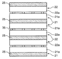
図2等に示すように、PDP1では、ガラス製の表面基板20と、ガラス製の背面基板30とが放電空間40を挟んで対向して配置され、放電空間40には放電によって紫外線を放射するガス(ネオン、キセノン等)が封入されている。表面基板20上には、誘電体層23及び保護膜24で覆われ且つ対をなす帯状の走査電極21及び維持電極22からなる電極群が、互いに平行になるように配列されている。走査電極21及び維持電極22は、それぞれ透明電極21a,22aと、透明電極21a,22a上に重なるように形成され且つ導電性を高めるための銀等からなる金属母線21b,22bとから構成されている。
As shown in FIG. 2 and the like, in the
また、図3に示すように、走査電極21と維持電極22とは、走査電極、走査電極、維持電極、維持電極の順に配列された電極配列を単位として形成され、隣接する走査電極21間と、隣接する維持電極22間とには、黒色材料からなる光吸収層25が設けられる。
In addition, as shown in FIG. 3, the
一方、図2等に示すように、背面基板30上には、走査電極21及び維持電極22と直交する方向に、複数の帯状のデータ電極31が互いに平行に配列されている。また、背面基板30上には、走査電極21及び維持電極22とデータ電極31とで形成される複数の放電セルを区画するための障壁35が形成されている。障壁35により区画されたセル空間41の背面基板30側には、放電セルに対応して形成された蛍光体層36が設けられている。
On the other hand, as shown in FIG. 2 and the like, a plurality of strip-
また、図4等に示すように、障壁35は、縦壁部35a及び横壁部35bから構成され、縦壁部35aは、走査電極21及び維持電極22と直交する方向、すなわちデータ電極31と平行な方向に延び、横壁部35bは、縦壁部35aに交差するように形成される。したがって、縦壁部35a及び横壁部35bからセル空間41が形成されるとともに、セル空間41間に隙間部42が形成される。また、障壁35の横壁部35b間に形成された隙間部42の空間に対応する位置に、上記の光吸収層25が形成される。
Further, as shown in FIG. 4 and the like, the
背面基板30の隙間部42側には、隙間部42内の空間において走査電極21との間でプライミング放電を行うためのプライミング電極33が、隣接する走査電極21に対向し且つデータ電極31と直交する方向に形成され、放電セルに隣接するプライミングセルが形成される。プライミング電極33は、データ電極31を覆う誘電体層32上に形成され、データ電極31よりも隙間部42内の空間に近い位置に形成される。
On the
また、プライミング電極33は、書き込みパルスが印加される走査電極21が隣り合う部分に対応する隙間部42のみに形成され、一方の走査電極21の金属母線21bの一部は、隙間部42側に延出して光吸収層25上に形成される。表面基板20側に形成された隣接する2つの走査電極21のうち隙間部42の領域の方向に突出した金属母線21bと、背面基板30側に形成されたプライミング電極33との間でプライミング放電が行われる。
The priming
本実施の形態では、アドレスドライバ2、スキャンドライバ3、サステインドライバ4、放電発生回路9、セットアップ回路10,11、プライミング放電発生回路12及びプライミングドライバ13が第1乃至第3の駆動手段の一例に相当する。
In the present embodiment, the address driver 2, the
なお、本発明に適用可能なPDPは、上記の構成に特に限定されず、セル空間の間に隙間部を形成し、隙間部内の空間において表面基板と背面基板との間でプライミング放電を発生させることができれば、以下のように種々の変更が可能である。すなわち、パネル周辺部の表示領域以外の部分に表面基板と背面基板との間でプライミング放電を発生させる放電領域を形成してもよい。また、プライミング電極をデータ電極と平行に配置し、このプライミング電極と走査電極との間でプライミング放電を発生させてもよい。また、背面基板側に形成されるプライミング電極に加えて、表面基板側の隙間部に対応する領域に新たなプライミング電極を形成し、両プライミング電極間でプライミング放電を発生させてもよい。 Note that the PDP applicable to the present invention is not particularly limited to the above configuration, and a gap is formed between the cell spaces, and a priming discharge is generated between the front substrate and the rear substrate in the space within the gap. If possible, various modifications are possible as follows. That is, a discharge region that generates priming discharge between the front substrate and the rear substrate may be formed in a portion other than the display region in the peripheral portion of the panel. Further, the priming electrode may be arranged in parallel with the data electrode, and priming discharge may be generated between the priming electrode and the scanning electrode. Further, in addition to the priming electrode formed on the back substrate side, a new priming electrode may be formed in a region corresponding to the gap portion on the front substrate side to generate priming discharge between both priming electrodes.
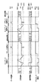
次に、上記のように構成されたプラズマディスプレイ装置の動作について説明する。図8は、図1に示すプラズマディスプレイ装置の駆動波形の一例を示す図である。なお、図8に示す各駆動パルスの電圧は一例であり、PDP1の放電特性等に応じて適宜変更可能である。この点について他の実施の形態も同様である。
Next, the operation of the plasma display device configured as described above will be described. FIG. 8 is a diagram showing an example of a driving waveform of the plasma display device shown in FIG. Note that the voltage of each drive pulse shown in FIG. 8 is an example, and can be appropriately changed according to the discharge characteristics of the
本実施の形態では、1フィールドが複数のサブフィールドに分割され、図8に示す最初のセットアップ期間S1、アドレス期間A1及び維持期間U1は、最初のサブフィールドに対応する期間であり、1垂直同期期間すなわちフィールドごとに1回設けられる期間である。後続のセットアップ期間S2、アドレス期間A2及び維持期間U2は、最初のサブフィールド以降の各サブフィールドに対応する期間であり、後続の各サブフィールドにおいてセットアップ期間S2、アドレス期間A2及び維持期間U2が繰り返される。なお、維持期間U1と維持期間U2との駆動波形はパルス数等を除き基本的に同一である。 In this embodiment, one field is divided into a plurality of subfields, and the first setup period S1, address period A1, and sustain period U1 shown in FIG. 8 are periods corresponding to the first subfield, and one vertical synchronization is performed. This is a period, that is, a period provided once for each field. The subsequent setup period S2, address period A2, and sustain period U2 are periods corresponding to the subfields after the first subfield, and the setup period S2, address period A2, and sustain period U2 are repeated in each subsequent subfield. It is. The drive waveforms in sustain period U1 and sustain period U2 are basically the same except for the number of pulses.
まず、最初のサブフィールドのセットアップ期間S1において、アドレスドライバ2は、データ電極31を0Vに保持する。スキャンドライバ3は、走査電極21の電圧をランプ波形により0Vから−170Vまで順次降下させ、その後、走査電極21の電圧を−170Vから0Vに立ち上げる。サステインドライバ4は、垂直同期期間に1回印加される垂直同期用セットアップパルスを印加して維持電極22の電圧を0Vから350Vに立ち上げて保持し、走査電極21が−170Vから0Vに立ち上げられたときに、維持電極22の電圧を350Vから0Vに立ち下げて保持する。このとき、走査電極21、維持電極22及びデータ電極31の三電極間で壁電荷を調整するセットアップ放電が発生し、走査電極21に正電荷が、維持電極22に負電荷が、データ電極31に負電荷がそれぞれ均一に且つ全面に蓄積される。なお、垂直同期用セットアップパルスの電圧としては、350Vに特に限定されず、300V〜350Vの範囲内で他の電圧を用いてもよい。
First, in the setup period S1 of the first subfield, the address driver 2 holds the
また、最初のサブフィールドのセットアップ期間S1において、プライミングドライバ13は、プライミング電極33の電圧を−100Vから0Vに立ち上げて保持し、走査電極21が−170Vから0Vに立ち上げられたときに、プライミング電極33の電圧を0Vから−100Vに立ち下げて保持する。このとき、走査電極21とプライミング電極33との間で壁電荷を調整するセットアップ放電が発生し、プライミング電極33に正電荷が蓄積される。また、上記の期間において、維持電極22が350Vに立ち上げられて保持されているときにプライミング電極33も0Vに立ち上げられて保持されているので、上記の走査電極21と維持電極22との間の放電を安定に行いながら、維持電極22とプライミング電極33との間で不要な放電が発生することを防止することができ、電極間の干渉をなくすことができる。
In the setup period S1 of the first subfield, the priming
次に、スキャンドライバ3は、走査電極21の電圧をランプ波形により0Vから250Vまで順次上昇させた後、走査電極21の電圧を250Vから0Vに立ち下げ、さらに、ランプ波形により0Vから−170Vまで順次降下させる。サステインドライバ4は、走査電極21の電圧がランプ波形により0Vから−170Vに降下しているときに、維持電極22の電圧を0Vから50Vに立ち上げて保持する。このとき、走査電極21と維持電極22との間で微弱な放電が発生し、走査電極21の維持電極側の一部の正電荷のみが負電荷に反転し、維持電極22の走査電極側の一部の負電荷のみが正電荷に反転する。また、このとき、プライミングドライバ13は、プライミング電極33の電圧を−100Vから0Vに立ち上げて保持している。
Next, the
また、垂直同期期間に1回設けられるセットアップ期間S1は、他のセットアップ期間S2より長く設定されているので、垂直同期期間に1回設けられるセットアップ期間S1において各電極の壁電荷を充分に調整し、その後のプライミング放電をより安定に発生させることができる。 Further, since the setup period S1 provided once in the vertical synchronization period is set longer than the other setup periods S2, the wall charge of each electrode is sufficiently adjusted in the setup period S1 provided once in the vertical synchronization period. The subsequent priming discharge can be generated more stably.
次に、アドレス期間A1において、まず、スキャンドライバ3は、走査電極21の電圧を−170Vから−50Vに立ち上げて保持し、その後、サステインドライバ4は、維持電極22の電圧を50Vから150Vに立ち上げて保持し、その後、プライミングドライバ13は、プライミング電極33の電圧を0Vから100Vに立ち上げて保持している。このように、アドレス期間A1において、壁電荷が調整された走査電極21の電圧を所定の電圧に立ち上げた後にプライミング電極33の電圧を所定の電圧に立ち上げているので、その後のプライミング放電をより安定に発生させることができる。他のアドレス期間A2も同様である。
Next, in the address period A1, first, the
次に、アドレスドライバ2は、正の書き込みパルスを印加してデータ電極31の電圧を0Vから70Vに立ち上げ、スキャンドライバ3は、負の書き込みパルスを印加して走査電極21の電圧を−50Vから−180Vに立ち下げると、走査電極21とプライミング電極33との間でプライミング放電が発生し、このプライミング放電を利用してデータ電極31と走査電極21との間で書き込み放電が発生する。所定時間経過後、スキャンドライバ3は、走査電極21の電圧を−50Vから0Vに立ち上げて保持する。
Next, the address driver 2 applies a positive write pulse to raise the voltage of the data electrode 31 from 0V to 70V, and the
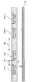
図9は、データ電極と走査電極との間で発生する書き込み放電を説明するための模式図である。図9に示すように、書き込みパルスを印加する前は、走査電極21nの維持電極22n側の一部のみに負電荷が蓄積され、その他の部分すなわち走査電極21nの走査電極(図示省略)側には正電荷が蓄積され、一方、維持電極22nの走査電極21n側の一部のみに正電荷が蓄積され、その他の部分すなわち維持電極22nの維持電極22n+1側には負電荷が蓄積され、維持電極22n+1及び走査電極21n+1にも同様に電荷が蓄積されている。
FIG. 9 is a schematic diagram for explaining the write discharge generated between the data electrode and the scan electrode. As shown in FIG. 9, before applying the write pulse, negative charges are accumulated only in a part of the
このとき、書き込みパルスが印加されると、走査電極21nとプライミング電極33(図示省略)との間でプライミング放電が発生し、このプライミング放電を利用してデータ電極31と走査電極21nとの間で弱い書き込み放電が発生し、この弱い書き込み放電をトリガーとして走査電極21nと維持電極22nとの間で弱い放電が発生する。この走査電極21nと維持電極22nとの間の放電は、走査電極21nと維持電極22nとの間の放電ギャップG1付近のみで発生するとともに、維持電極22nと維持電極22n+1との間のギャップG2には、電子による電位障壁が形成されているため、走査電極21nと維持電極22nとの間の放電が維持電極22n+1側に広がることを防止することができ、隣接するライン間のクロストークを防止することができる。
At this time, when a write pulse is applied, a priming discharge is generated between the
次に、維持期間U1において、スキャンドライバ3は、走査電極21に200Vの維持パルスを順次印加し、サステインドライバ4は、走査電極21の維持パルスに対して180°位相のずれた200Vの維持パルスを維持電極22に順次印加し、維持放電を発光輝度に応じた回数だけ繰り返し発生させる。また、プライミングドライバ13は、走査電極21への最初の維持パルスが立ち上がるときに、プライミング電極33の電圧を100Vから−100Vに立ち下げて保持する。このとき、走査電極21とプライミング電極33との間で放電が発生し、プライミング電極33に正電荷が蓄積される。
Next, in the sustain period U1, the
また、維持期間U1において、スキャンドライバ3は、最後の維持パルスとして、他の維持パルスよりハイ期間が長い維持パルスを走査電極21に印加し、サステインドライバ4は、走査電極21への最後の維持パルスが200Vから0Vに立ち下がったときに、0Vから200Vに立ち上がる最後の維持パルスを維持電極22に印加する。このように、走査電極21への最後の維持周期を下げた状態で、維持電極22に印加される最後の維持パルスを立ち上げることにより、走査電極21と維持電極22との間で強い維持放電が発生し、走査電極21に正電荷が、維持電極22に負電荷がそれぞれ均一に且つ全面に蓄積される。
In the sustain period U1, the
次のサブフィールドのセットアップ期間S2において、スキャンドライバ3は、走査電極21の電圧をランプ波形により0Vから250Vまで順次上昇させた後、走査電極21の電圧を250Vから0Vに立ち下げ、さらに、ランプ波形により0Vから−170Vまで順次降下させる。サステインドライバ4は、走査電極21の電圧がランプ波形により0Vから降下するときに、維持電極22の電圧を0Vから50Vに立ち上げて保持する。このとき、走査電極21と維持電極22との間で微弱な放電が発生し、走査電極21の維持電極側の一部の正電荷のみが負電荷に反転し、維持電極22の走査電極側の一部の負電荷のみが正電荷に反転する。また、このとき、プライミングドライバ13は、プライミング電極33の電圧を−100Vから0Vに立ち上げて保持している。
In the setup period S2 of the next subfield, the
次に、アドレス期間A2において、まず、スキャンドライバ3は、走査電極21の電圧を−170Vから−50Vに立ち上げて保持し、サステインドライバ4は、維持電極22の電圧を50Vから150Vに立ち上げて保持し、その後、プライミングドライバ13は、プライミング電極33の電圧を0Vから100Vに立ち上げて保持する。
Next, in the address period A2, first, the
次に、アドレスドライバ2は、正の書き込みパルスを印加してデータ電極31の電圧を0Vから70Vに立ち上げ、スキャンドライバ3は、負の書き込みパルスを印加して走査電極21の電圧を−50Vから−180Vに立ち下げると、走査電極21とプライミング電極33との間でプライミング放電が発生し、このプライミング放電を利用してデータ電極31と走査電極21との間で書き込み放電が発生する。所定時間経過後、スキャンドライバ3は、走査電極21の電圧を−50Vから0Vに立ち上げて保持する。
Next, the address driver 2 applies a positive write pulse to raise the voltage of the data electrode 31 from 0V to 70V, and the
この場合もアドレス期間A1と同様に、書き込みパルスを印加する前は、走査電極21の維持電極側の一部のみに負電荷が蓄積され、維持電極22の走査電極側の一部のみに正電荷が蓄積されている。このとき、書き込みパルスが印加されると、走査電極21とプライミング電極33との間でプライミング放電が発生し、このプライミング放電を利用してデータ電極31と走査電極21との間で弱い書き込み放電が発生し、この弱い書き込み放電をトリガーとして走査電極21と維持電極22との間の放電ギャップ付近のみで弱い放電が発生するとともに、維持電極22間のギャップには電子による電位障壁が形成されているため、走査電極21と維持電極22との間の放電が隣接する維持電極22側に広がることを防止することができ、クロストークを防止することができる。
Also in this case, as in the address period A1, negative charges are accumulated only in a part of the sustain electrode side of the
次に、維持期間U2において、維持期間U1と同様の動作が行われ、プライミング電極33に正電荷が蓄積されるとともに、維持放電が行われ、最後の維持放電により走査電極21に正電荷が、維持電極22に負電荷がそれぞれ均一に且つ全面に蓄積される。その後、セットアップ期間S2、アドレス期間A2及び維持期間U2の動作がサブフィールドごとに繰り返されて1フィールド期間の動作が完了する。
Next, in the sustain period U2, the same operation as in the sustain period U1 is performed, positive charges are accumulated in the priming
上記のように、本実施の形態では、セットアップ期間において、前サブフィールドで維持放電を行った走査電極21及び維持電極22の壁電荷を調整しているので、維持放電により減少した走査電極21の壁電荷を補充することができ、アドレス期間において書き込み放電を安定に行うことができる。また、アドレス期間において走査電極21とプライミング電極33との間のプライミング放電を利用して書き込み放電を発生させているので、書き込み放電を弱い放電で安定に行うことができる。したがって、書き込み放電による不要光を低減することができ、無信号時における黒輝度を充分に低くすることができる。
As described above, in the present embodiment, the wall charges of
また、維持期間において、書き込み放電が発生した走査電極21の維持放電後に走査電極21の全面に正電荷を蓄積させ、セットアップ期間において、蓄積された走査電極21の正電荷のうち維持電極22側の一部の正電荷を負電荷に反転させるとともに、蓄積された維持電極22の負電荷のうち走査電極21側の一部の負電荷を正電荷に反転させているので、隣接する維持電極22間には負電荷が残留することになる。したがって、隣接する放電セル間においてこの負電荷が電位障壁として機能し、一方の放電セルのアドレス期間における書き込み放電が他方の放電セルに広がることを防止することができるので、隣接する放電セル間のクロストークを充分に低減することができる。
Further, in the sustain period, positive charges are accumulated on the entire surface of the
さらに、セットアップ期間における一部の電荷の反転は低い電位により発生させることができるので、セットアップ回路10等の低コスト化を図ることができる。
Further, inversion of some charges in the setup period can be generated with a low potential, so that the cost of the
次に、本発明の第2の実施の形態によるプラズマディスプレイ装置について説明する。図10は、本発明の第2の実施の形態によるプラズマディスプレイ装置の駆動波形の一例を示す図である。なお、本実施の形態によるプラズマディスプレイ装置の構成は、PDP1に印加される駆動波形が異なる点を除き、図1に示すプラズマディスプレイ装置と同様であるため、図示を省略して図1を用いてその構成を説明する。この点について以下の各実施の形態も同様である。
Next, a plasma display apparatus according to a second embodiment of the present invention will be described. FIG. 10 is a diagram illustrating an example of a driving waveform of the plasma display apparatus according to the second embodiment of the present invention. The configuration of the plasma display device according to the present embodiment is the same as that of the plasma display device shown in FIG. 1 except that the driving waveform applied to the
図10に示す駆動波形と図8に示す駆動波形とで異なる点は、垂直同期用セットアップパルスが変更された点であり、その他の点は図8に示す駆動波形と同様であるので、以下異なる点についてのみ詳細に説明する。 The difference between the drive waveform shown in FIG. 10 and the drive waveform shown in FIG. 8 is that the vertical synchronization setup pulse is changed, and the other points are the same as the drive waveform shown in FIG. Only the point will be described in detail.
図10に示すように、最初のサブフィールドのセットアップ期間S1において、サステインドライバ4は、プラズマディスプレイ装置の電源がオンされたとき、350Vの垂直同期用セットアップパルスV1を維持電極22に印加し、その後に印加する垂直同期用セットアップパルスとして、図中に破線で示す200Vの垂直同期用セットアップパルスV2を維持電極22に印加する。
As shown in FIG. 10, in the setup period S1 of the first subfield, the sustain driver 4 applies a vertical synchronization setup pulse V1 of 350 V to the sustain
装置の電源がオンされたときは、壁電荷の調整が何ら行われていないため、各電極の壁電荷の状態が異常な状態になっている場合があり、この場合でも、350Vの垂直同期用セットアップパルスV1を印加することにより、走査電極21、維持電極22及びデータ電極31の三電極間に強いセットアップ放電を発生させることができ、走査電極21に正電荷を、維持電極22に負電荷を、データ電極31に負電荷をそれぞれ均一に且つ全面に安定的に蓄積することができる。
When the power of the device is turned on, the wall charge is not adjusted at all, so the wall charge of each electrode may be in an abnormal state. By applying the setup pulse V1, a strong setup discharge can be generated between the
一方、その他の場合、既に壁電荷の調整が行われているため、垂直同期用セットアップパルスの電圧を極限まで低下させることができ、例えば、200Vの垂直同期用セットアップパルスV2を印加することにより、走査電極21、維持電極22及びデータ電極31の三電極間に弱いセットアップ放電を安定に発生させることができ、走査電極21に正電荷を、維持電極22に負電荷を、データ電極31に負電荷をそれぞれ均一に且つ全面に蓄積することができる。
On the other hand, since the wall charge has already been adjusted in other cases, the voltage of the vertical synchronization setup pulse can be reduced to the limit. For example, by applying the vertical synchronization setup pulse V2 of 200V, A weak setup discharge can be stably generated between the
このように、本実施の形態では、第1の実施の形態の効果に加えて、装置の電源がオンされたとき以外は、弱いセットアップ放電を安定に発生させることができるので、無信号時における黒輝度をより低くすることができ、画像品質をより向上することができる。 Thus, in this embodiment, in addition to the effect of the first embodiment, a weak setup discharge can be stably generated except when the apparatus is turned on. The black luminance can be further reduced, and the image quality can be further improved.
なお、高電位の垂直同期用セットアップパルスV1の印加タイミングは、装置の電源がオンされたときのみに特に限定されず、通常描画時以外の異常事態、例えば、映像信号の入力切替が行われたとき、チャンネル切替が行われたとき等においても高電位の垂直同期用セットアップパルスを印加するようにしてもよい。 Note that the application timing of the high-potential vertical synchronization setup pulse V1 is not particularly limited only when the power of the apparatus is turned on, and an abnormal situation other than normal drawing, for example, switching of video signal input is performed. At this time, a high-potential vertical synchronization setup pulse may be applied even when the channel is switched.
次に、本発明の第3の実施の形態によるプラズマディスプレイ装置について説明する。図11は、本発明の第3の実施の形態によるプラズマディスプレイ装置の駆動波形の一例を示す図である。 Next, a plasma display apparatus according to a third embodiment of the present invention is described. FIG. 11 is a diagram illustrating an example of a driving waveform of the plasma display device according to the third embodiment of the present invention.
図11に示す駆動波形と図8に示す駆動波形とで異なる点は、プライミング電極33に印加されるパルスが変更された点であり、その他の点は図8に示す駆動波形と同様であるので、以下異なる点についてのみ詳細に説明する。
The difference between the drive waveform shown in FIG. 11 and the drive waveform shown in FIG. 8 is that the pulse applied to the priming
図11に示すように、維持期間U1において、プライミングドライバ13は、走査電極21への最後の維持パルスが立ち上がるときに、プライミング電極33の電圧を100Vから−100Vに立ち下げて保持する。このとき、走査電極21とプライミング電極33との間で放電が発生し、プライミング電極33に正電荷が蓄積される。この場合、壁電荷の調整後から後続のセットアップ期間S2までの時間を短縮することができ、後続のセットアップ期間S2におけるセットアップ放電に走査電極21とプライミング電極33との間の放電によるプライミング効果を利用することができる。
As shown in FIG. 11, in the sustain period U1, the priming
このように、本実施の形態では、第1の実施の形態の効果に加えて、後続のセットアップ期間S2におけるセットアップ放電に走査電極21とプライミング電極33との間の放電によるプライミング効果を利用することができるので、セットアップ放電が弱い放電である場合でも、セットアップ放電を安定に行うことができ、セットアップ期間における不要光を低減して黒輝度を低減することができるとともに、書き込み放電も安定に行うことができる。
Thus, in this embodiment, in addition to the effect of the first embodiment, the priming effect by the discharge between the
次に、本発明の第4の実施の形態によるプラズマディスプレイ装置について説明する。図12は、本発明の第4の実施の形態によるプラズマディスプレイ装置の駆動波形の一例を示す図である。 Next, a plasma display apparatus according to a fourth embodiment of the present invention is described. FIG. 12 is a diagram illustrating an example of a driving waveform of the plasma display device according to the fourth embodiment of the present invention.
図12に示す駆動波形と図8に示す駆動波形とで異なる点は、垂直同期用セットアップパルス及びプライミング電極33に印加されるパルスが変更された点であり、その他の点は図8に示す駆動波形と同様であるので、以下異なる点についてのみ詳細に説明する。
The difference between the drive waveform shown in FIG. 12 and the drive waveform shown in FIG. 8 is that the setup pulse for vertical synchronization and the pulse applied to the priming
図12に示すように、第2の実施形態と同様に、最初のサブフィールドのセットアップ期間S1において、サステインドライバ4は、プラズマディスプレイ装置の電源がオンされたときは、350Vの垂直同期用セットアップパルスV1を維持電極22に印加し、その後に印加する垂直同期用セットアップパルスとして、200Vの垂直同期用セットアップパルスV2を維持電極22に印加する。
As shown in FIG. 12, in the setup period S1 of the first subfield, the sustain driver 4 sets the 350 V vertical synchronization setup pulse when the power of the plasma display device is turned on, as in the second embodiment. V1 is applied to the sustain
また、第3の実施の形態と同様に、維持期間U1において、プライミングドライバ13は、走査電極への最後の維持パルスが立ち上がるときに、プライミング電極33の電圧を100Vから−100Vに立ち下げ、走査電極21とプライミング電極33との間で放電が発生し、プライミング電極33に正電荷が蓄積される。したがって、本実施の形態では、第1の実施の形態の効果に加えて、第2及び第3の実施の形態による効果を得ることができる。
Similarly to the third embodiment, during the sustain period U1, the priming
次に、本発明の第5の実施の形態によるプラズマディスプレイ装置について説明する。図13は、本発明の第5の実施の形態によるプラズマディスプレイ装置の駆動波形の一例を示す図である。 Next, a plasma display apparatus according to a fifth embodiment of the present invention is described. FIG. 13 is a diagram showing an example of a driving waveform of the plasma display device according to the fifth embodiment of the present invention.
図13に示す駆動波形と図8に示す駆動波形とで異なる点は、プライミング電極33に印加されるパルスが変更された点であり、その他の点は図8に示す駆動波形と同様であるので、以下異なる点についてのみ詳細に説明する。
The difference between the drive waveform shown in FIG. 13 and the drive waveform shown in FIG. 8 is that the pulse applied to the priming
図13に示すように、セットアップ期間S1,S2において、プライミングドライバ13は、プライミング電極33の電圧を100Vに保持し、走査電極21の電圧がランプ波形により0Vから250Vまで上昇されているときに、プライミング電極33の電圧を100Vから−100Vに立ち下げて保持する。このとき、走査電極21とプライミング電極33との間で放電が発生し、プライミング電極33に正電荷が蓄積される。
As shown in FIG. 13, in the setup periods S1 and S2, the priming
次に、スキャンドライバ3は、走査電極21の電圧を250Vから0Vに立ち下げ、さらに、ランプ波形により0Vから−170Vまで順次降下させる。サステインドライバ4は、走査電極21の電圧がランプ波形により0Vから−170Vに降下しているときに、維持電極22の電圧を0Vから50Vに立ち上げて保持する。このとき、上記の走査電極21とプライミング電極33との間の放電によるプライミング効果を利用して、走査電極21と維持電極22との間で微弱な放電を安定に発生させ、走査電極21の維持電極側の一部の正電荷のみを負電荷に反転させ、維持電極22の走査電極側の一部の負電荷のみを正電荷に反転させる。
Next, the
このように、本実施の形態では、第1の実施の形態の効果に加えて、セットアップ期間において走査電極21と維持電極22との放電前に走査電極21とプライミング電極33との間に放電を発生させてプライミング電極33の壁電荷を調整しているので、走査電極21とプライミング電極33との放電によるプライミング効果を走査電極21と維持電極22とのセットアップ放電に利用することができ、セットアップ放電が弱い放電である場合でも、セットアップ放電を安定に行うことができるので、セットアップ期間における不要光を低減して黒輝度をより低減することができるとともに、書き込み放電も安定に行うことができる。
Thus, in the present embodiment, in addition to the effects of the first embodiment, a discharge is generated between the
次に、本発明の第6の実施の形態によるプラズマディスプレイ装置について説明する。図14は、本発明の第6の実施の形態によるプラズマディスプレイ装置の駆動波形の一例を示す図である。 Next, a plasma display apparatus according to a sixth embodiment of the present invention is described. FIG. 14 is a diagram showing an example of a driving waveform of the plasma display apparatus according to the sixth embodiment of the present invention.
図14に示す駆動波形と図8に示す駆動波形とで異なる点は、垂直同期用セットアップパルス及びプライミング電極33に印加されるパルスが変更された点であり、その他の点は図8に示す駆動波形と同様であるので、以下異なる点についてのみ詳細に説明する。
The difference between the drive waveform shown in FIG. 14 and the drive waveform shown in FIG. 8 is that the setup pulse for vertical synchronization and the pulse applied to the priming
図14に示すように、第2の実施形態と同様に、最初のサブフィールドのセットアップ期間S1において、サステインドライバ4は、プラズマディスプレイ装置の電源がオンされたときは、350Vの垂直同期用セットアップパルスV1を維持電極22に印加し、その後に印加する垂直同期用セットアップパルスとして、200Vの垂直同期用セットアップパルスV2を維持電極22に印加する。
As shown in FIG. 14, in the setup period S1 of the first subfield, as in the second embodiment, the sustain driver 4 sets the 350 V vertical synchronization setup pulse when the power of the plasma display device is turned on. V1 is applied to the sustain
また、第5の実施の形態と同様に、セットアップ期間S1,S2において、プライミングドライバ13は、走査電極21の電圧がランプ波形により上昇されているときに、プライミング電極33の電圧を100Vから−100Vに立ち下げて保持し、走査電極21とプライミング電極33との間で放電を発生させてプライミング電極33に正電荷を蓄積する。次に、スキャンドライバ3は、走査電極21の電圧をランプ波形により降下させているときに、サステインドライバ4は、維持電極22の電圧を立ち上げ、上記の走査電極21とプライミング電極33との間の放電によるプライミング効果を利用して、走査電極21と維持電極22との間で微弱な放電を安定に発生させ、走査電極21の維持電極側の一部の正電荷のみを負電荷に反転させ、維持電極22の走査電極側の一部の負電荷のみを正電荷に反転させる。したがって、本実施の形態では、第1の実施の形態の効果に加えて、第2及び第5の実施の形態による効果を得ることができる。
Similarly to the fifth embodiment, in the setup periods S1 and S2, the priming
次に、本発明の第7の実施の形態によるプラズマディスプレイ装置について説明する。図15は、本発明の第7の実施の形態によるプラズマディスプレイ装置の駆動波形の一例を示す図である。 Next, a plasma display apparatus according to a seventh embodiment of the present invention is described. FIG. 15 is a diagram showing an example of a driving waveform of the plasma display device according to the seventh embodiment of the present invention.
図15に示す駆動波形と図8に示す駆動波形とで異なる点は、プライミング電極33に印加されるパルスが変更された点であり、その他の点は図8に示す駆動波形と同様であるので、以下異なる点についてのみ詳細に説明する。
The drive waveform shown in FIG. 15 differs from the drive waveform shown in FIG. 8 in that the pulse applied to the priming
図15に示すように、プライミングドライバ13は、セットアップ期間S1,S2においてプライミング電極33の電圧を0Vに保持し、アドレス期間A1,A2においてプライミング電極33の電圧を0Vから100Vに立ち上げて保持し、維持期間U1,U2において、走査電極21への最初の維持パルスが立ち上がるときに、プライミング電極33の電圧を100Vから0Vに立ち下げて保持する。このとき、走査電極21とプライミング電極33との間で放電が発生し、プライミング電極33に正電荷が蓄積される。
As shown in FIG. 15, the priming
このように、本実施の形態では、第1の実施の形態の効果に加えて、プライミング電極33に印加する電圧を0Vと100Vとの2値にしているので、プライミングドライバ13の構成を簡略化することができるとともに、消費電力及び電磁波障害を低減することができる。
As described above, in this embodiment, in addition to the effects of the first embodiment, the voltage applied to the priming
次に、本発明の第8の実施の形態によるプラズマディスプレイ装置について説明する。図16は、本発明の第8の実施の形態によるプラズマディスプレイ装置の駆動波形の一例を示す図である。 Next, a plasma display apparatus according to an eighth embodiment of the present invention is described. FIG. 16 is a diagram showing an example of a driving waveform of the plasma display device according to the eighth embodiment of the present invention.
図16に示す駆動波形と図8に示す駆動波形とで異なる点は、垂直同期用セットアップパルス及びプライミング電極33に印加されるパルスが変更された点であり、その他の点は図8に示す駆動波形と同様であるので、以下異なる点についてのみ詳細に説明する。
The drive waveform shown in FIG. 16 differs from the drive waveform shown in FIG. 8 in that the setup pulse for vertical synchronization and the pulse applied to the priming
図16に示すように、第2の実施形態と同様に、最初のサブフィールドのセットアップ期間S1において、サステインドライバ4は、プラズマディスプレイ装置の電源がオンされたときは、350Vの垂直同期用セットアップパルスV1を維持電極22に印加し、その後に印加する垂直同期用セットアップパルスとして、200Vの垂直同期用セットアップパルスV2を維持電極22に印加する。
As shown in FIG. 16, in the setup period S1 of the first subfield, as in the second embodiment, the sustain driver 4 sets the 350 V vertical synchronization setup pulse when the power of the plasma display device is turned on. V1 is applied to the sustain
また、第7の実施の形態と同様に、プライミングドライバ13は、セットアップ期間S1,S2においてプライミング電極33の電圧を0Vに保持し、アドレス期間A1,A2においてプライミング電極33の電圧を0Vから100Vに立ち上げて保持し、維持期間U1,U2において、走査電極21への最初の維持パルスが立ち上がるときに、プライミング電極33の電圧を100Vから0Vに立ち下げて保持し、走査電極21とプライミング電極33との間で放電を発生させ、プライミング電極33に正電荷を蓄積させる。したがって、本実施の形態では、第1の実施の形態の効果に加えて、第2及び第7の実施の形態による効果を得ることができる。
Similarly to the seventh embodiment, the priming
次に、本発明の第9の実施の形態によるプラズマディスプレイ装置について説明する。図17は、本発明の第9の実施の形態によるプラズマディスプレイ装置の駆動波形の一例を示す図である。 Next, a plasma display apparatus according to a ninth embodiment of the present invention is described. FIG. 17 is a diagram showing an example of a driving waveform of the plasma display device according to the ninth embodiment of the present invention.
図17に示す駆動波形と図8に示す駆動波形とで異なる点は、プライミング電極33に印加されるパルスが変更された点であり、その他の点は図8に示す駆動波形と同様であるので、以下異なる点についてのみ詳細に説明する。
The difference between the drive waveform shown in FIG. 17 and the drive waveform shown in FIG. 8 is that the pulse applied to the priming
図17に示すように、プライミングドライバ13は、セットアップ期間S1,S2においてプライミング電極33の電圧を0Vに保持し、アドレス期間A1,A2においてプライミング電極33の電圧を0Vから100Vに立ち上げて保持し、維持期間U1,U2において、第3の実施の形態と同様に走査電極21への最後の維持パルスが立ち上がるときに、プライミング電極33の電圧を100Vから0Vに立ち下げて保持する。このとき、走査電極21とプライミング電極33との間で放電が発生し、プライミング電極33に正電荷が蓄積される。
As shown in FIG. 17, the priming
このように、本実施の形態では、第1及び第3の実施の形態の効果に加えて、プライミング電極33に印加する電圧を0Vと100Vとの2値にしているので、プライミングドライバ13の構成を簡略化することができるとともに、消費電力及び電磁波障害を低減することができる。
Thus, in this embodiment, in addition to the effects of the first and third embodiments, the voltage applied to the priming
次に、本発明の第10の実施の形態によるプラズマディスプレイ装置について説明する。図18は、本発明の第10の実施の形態によるプラズマディスプレイ装置の駆動波形の一例を示す図である。 Next, a plasma display apparatus according to a tenth embodiment of the present invention is described. FIG. 18 is a diagram showing an example of a driving waveform of the plasma display device according to the tenth embodiment of the present invention.
図18に示す駆動波形と図8に示す駆動波形とで異なる点は、垂直同期用セットアップパルス及びプライミング電極33に印加されるパルスが変更された点であり、その他の点は図8に示す駆動波形と同様であるので、以下異なる点についてのみ詳細に説明する。
The drive waveform shown in FIG. 18 differs from the drive waveform shown in FIG. 8 in that the vertical synchronization setup pulse and the pulse applied to the priming
図18に示すように、第2の実施形態と同様に、最初のサブフィールドのセットアップ期間S1において、サステインドライバ4は、プラズマディスプレイ装置の電源がオンされたときは、350Vの垂直同期用セットアップパルスV1を維持電極22に印加し、その後に印加する垂直同期用セットアップパルスとして、200Vの垂直同期用セットアップパルスV2を維持電極22に印加する。
As shown in FIG. 18, in the setup period S1 of the first subfield, as in the second embodiment, the sustain driver 4 sets the 350 V vertical synchronization setup pulse when the power of the plasma display device is turned on. V1 is applied to the sustain
また、第9の実施の形態と同様に、セットアップ期間S1,S2においてプライミング電極33の電圧を0Vに保持し、アドレス期間A1,A2においてプライミング電極33の電圧を0Vから100Vに立ち上げて保持し、維持期間U1,U2において、走査電極21への最後の維持パルスが立ち上がるときに、プライミング電極33の電圧を100Vから0Vに立ち下げて保持する。このとき、走査電極21とプライミング電極33との間で放電が発生し、プライミング電極33に正電荷が蓄積される。したがって、本実施の形態では、第1の実施の形態の効果に加えて、第2及び第9の実施の形態による効果を得ることができる。
Similarly to the ninth embodiment, the voltage of the priming
次に、本発明の第11の実施の形態によるプラズマディスプレイ装置について説明する。図19は、本発明の第11の実施の形態によるプラズマディスプレイ装置の駆動波形の一例を示す図である。 Next, a plasma display apparatus according to an eleventh embodiment of the present invention is described. FIG. 19 is a diagram showing an example of a driving waveform of the plasma display device according to the eleventh embodiment of the present invention.
図19に示す駆動波形と図8に示す駆動波形とで異なる点は、プライミング電極33に印加されるパルスが変更された点であり、その他の点は図8に示す駆動波形と同様であるので、以下異なる点についてのみ詳細に説明する。
The drive waveform shown in FIG. 19 is different from the drive waveform shown in FIG. 8 in that the pulse applied to the priming
図19に示すように、セットアップ期間S1において、プライミングドライバ13は、プライミング電極33の電圧を0Vに保持し、走査電極21の電圧がランプ波形により0Vから250Vまで上昇されているときに、プライミング電極33の電圧を0Vから100Vに立ち上げて所定時間保持した後に100Vから0Vに立ち下げて保持する。この場合、プライミング電極33の電圧が100Vから0Vに立ち下がるときに、走査電極21とプライミング電極33との間で放電が発生し、プライミング電極33に正電荷が蓄積される。
As shown in FIG. 19, in the setup period S1, the priming
次に、スキャンドライバ3は、走査電極21の電圧を250Vから0Vに立ち下げ、さらに、ランプ波形により0Vから−170Vまで順次降下させる。サステインドライバ4は、走査電極21の電圧がランプ波形により0Vから−170Vに降下しているときに、維持電極22の電圧を0Vから150Vに立ち上げて保持する。このとき、上記の走査電極21とプライミング電極33との間の放電によるプライミング効果を利用して、走査電極21と維持電極22との間で微弱な放電を安定に発生させ、走査電極21の維持電極側の一部の正電荷のみを負電荷に反転させ、維持電極22の走査電極側の一部の負電荷のみを正電荷に反転させる。
Next, the
次に、プライミングドライバ13は、アドレス期間A1において、プライミング電極33の電圧を0Vから100Vに立ち上げて保持し、維持期間U1が経過した後、セットアップ期間S2において、走査電極21の電圧がランプ波形により0Vから250Vまで上昇されているときに、プライミング電極33の電圧を100Vから0Vに立ち下げて保持する。この場合も、プライミング電極33の電圧が100Vから0Vに立ち下がるときに、走査電極21とプライミング電極33との間で放電が発生し、プライミング電極33に正電荷が蓄積される。以降アドレス期間A2及び維持期間U2において、上記のアドレス期間A1及び維持期間U1と同様の動作が行われる。
Next, the priming
このように、本実施の形態では、第1の実施の形態の効果に加えて、走査電極21とプライミング電極33との放電によるプライミング効果を走査電極21と維持電極22とのセットアップ放電に利用することができるので、セットアップ放電が弱い放電である場合でも、セットアップ放電を安定に行うことができ、セットアップ期間における不要光を低減してより黒輝度を低減することができるとともに、書き込み放電も安定に行うことができる。また、プライミング電極33に印加する電圧を0Vと100Vとの2値にしているので、プライミングドライバ13の構成を簡略化することができるとともに、消費電力及び電磁波障害を低減することができる。
As described above, in this embodiment, in addition to the effects of the first embodiment, the priming effect by the discharge of the
次に、本発明の第12の実施の形態によるプラズマディスプレイ装置について説明する。図20は、本発明の第12の実施の形態によるプラズマディスプレイ装置の駆動波形の一例を示す図である。 Next, a plasma display apparatus according to a twelfth embodiment of the present invention is described. FIG. 20 is a diagram illustrating an example of a driving waveform of the plasma display device according to the twelfth embodiment of the present invention.
図20に示す駆動波形と図8に示す駆動波形とで異なる点は、垂直同期用セットアップパルス及びプライミング電極33に印加されるパルスが変更された点であり、その他の点は図8に示す駆動波形と同様であるので、以下異なる点についてのみ詳細に説明する。
The drive waveform shown in FIG. 20 differs from the drive waveform shown in FIG. 8 in that the setup pulse for vertical synchronization and the pulse applied to the priming
図20に示すように、第2の実施形態と同様に、最初のサブフィールドのセットアップ期間S1において、サステインドライバ4は、プラズマディスプレイ装置の電源がオンされたときは、350Vの垂直同期用セットアップパルスV1を維持電極22に印加し、その後に印加する垂直同期用セットアップパルスとして、200Vの垂直同期用セットアップパルスV2を維持電極22に印加する。
As shown in FIG. 20, in the setup period S1 of the first subfield, the sustain driver 4 sets the 350 V vertical synchronization setup pulse when the power of the plasma display device is turned on, as in the second embodiment. V1 is applied to the sustain
また、第11の実施の形態と同様に、セットアップ期間S1,S2において、プライミング電極33の電圧が100Vから0Vに立ち下がるときに、走査電極21とプライミング電極33との間で放電が発生し、プライミング電極33に正電荷が蓄積される。この走査電極21とプライミング電極33との間の放電によるプライミング効果を利用して、走査電極21と維持電極22との間で微弱な放電を安定に発生させ、走査電極21の維持電極22側の一部の正電荷のみを負電荷に反転させ、維持電極22の走査電極21側の一部の負電荷のみを正電荷に反転させる。したがって、本実施の形態では、第1の実施の形態の効果に加えて、第2及び第11の実施の形態による効果を得ることができる。
Similarly to the eleventh embodiment, when the voltage of the priming
なお、上記の各実施の形態では、ADS方式によるサブフィールド分割を例に説明したが、アドレス・サステイン同時駆動方式によるサブフィールド分割等の他のサブフィールド法であっても、本発明を同様に適用することができ、同様の効果を得ることができる。 In each of the above embodiments, subfield division by the ADS method has been described as an example. However, the present invention is similarly applied to other subfield methods such as subfield division by the address / sustain simultaneous drive method. The same effect can be obtained.
上記のように、本発明によれば、クロストークを充分に低減することができるとともに、無信号時における黒輝度を充分に低くすることができ、1フィールドを複数のサブフィールドに分割して階調表示を行うプラズマディスプレイ表示装置等に好適に利用することができる。 As described above, according to the present invention, the crosstalk can be sufficiently reduced, the black luminance at the time of no signal can be sufficiently reduced, and one field is divided into a plurality of subfields. The present invention can be suitably used for a plasma display device that performs tone display.
Claims (11)
走査電極、走査電極、維持電極、維持電極の順に配列された電極配列を単位として複数の走査電極及び複数の維持電極が形成されるとともに、隣接する走査電極に対向して複数のプライミング電極が形成され、さらに、前記走査電極及び前記維持電極と交わる方向に複数のデータ電極が形成されたAC型プラズマディスプレイパネルと、
セットアップ期間において、前サブフィールドで維持放電を行った走査電極及び維持電極の壁電荷を調整する第1の駆動手段と、
アドレス期間において、前記第1の駆動手段により壁電荷が調整された走査電極に書き込みパルスを印加して当該走査電極とプライミング電極との間のプライミング放電を発生させるとともに、前記データ電極に書き込みパルスを印加して前記プライミング放電を利用して書き込み放電を発生させる第2の駆動手段と、
維持期間において、前記第2の駆動手段により書き込み放電が発生した走査電極と維持電極との間で維持放電を発生させ、維持放電後に走査電極に正電荷及び維持電極に負電荷を蓄積させる第3の駆動手段とを備え、
前記第1の駆動手段は、セットアップ期間において、前記第3の駆動手段により蓄積された走査電極の正電荷のうち維持電極側の一部の正電荷を負電荷に反転させるとともに、前記第3の駆動手段により蓄積された維持電極の負電荷のうち走査電極側の一部の負電荷を正電荷に反転させることを特徴とするプラズマディスプレイ装置。A plasma display apparatus that performs gradation display by dividing one field into a plurality of subfields each including a setup period, an address period, and a sustain period,
A plurality of scan electrodes and a plurality of sustain electrodes are formed in units of electrode arrays arranged in the order of scan electrodes, scan electrodes, sustain electrodes, and sustain electrodes, and a plurality of priming electrodes are formed to face adjacent scan electrodes. And an AC type plasma display panel in which a plurality of data electrodes are formed in a direction intersecting with the scan electrodes and the sustain electrodes;
In the setup period, the first driving means for adjusting the wall charges of the scan electrode and the sustain electrode that have performed the sustain discharge in the previous subfield;
In the address period, a write pulse is applied to the scan electrode whose wall charge is adjusted by the first driving means to generate a priming discharge between the scan electrode and the priming electrode, and a write pulse is applied to the data electrode. Second driving means for applying and generating an address discharge using the priming discharge;
In the sustain period, a sustain discharge is generated between the scan electrode where the write discharge is generated by the second driving means and the sustain electrode, and after the sustain discharge, a positive charge is accumulated in the scan electrode and a negative charge is accumulated in the sustain electrode. Driving means,
In the setup period, the first driving unit inverts a part of the positive charges on the sustain electrode side among the positive charges of the scan electrodes accumulated by the third driving unit to negative charges, and the third driving unit A plasma display apparatus characterized in that a part of negative charges on the scanning electrode side among negative charges of the sustain electrodes accumulated by the driving means is inverted to positive charges.
前記第2の駆動手段は、アドレス期間において書き込み放電が発生する前に前記プライミング電極を前記第1の電圧から前記第1の電圧より高い第2の電圧に立ち上げて保持し、
前記第3の駆動手段は、維持期間において前記プライミング電極を前記第2の電圧から前記第1の電圧に立ち下げることを特徴とする請求項1記載のプラズマディスプレイ装置。The first driving means holds the priming electrode at a first voltage during a setup period,
The second driving means raises and holds the priming electrode from the first voltage to a second voltage higher than the first voltage before an address discharge occurs in an address period,
2. The plasma display apparatus according to claim 1, wherein the third driving unit drops the priming electrode from the second voltage to the first voltage in the sustain period.
前記第2の駆動手段は、アドレス期間において書き込み放電が発生する前に前記プライミング電極を前記第2の電圧から前記第1の電圧に立ち上げて保持することを特徴とする請求項6に記載のプラズマディスプレイ装置。The first driving means holds the priming electrode from the first voltage to a second voltage lower than the first voltage before the discharge of the scan electrode and the sustain electrode during the setup period,
7. The second drive unit according to claim 6, wherein the priming electrode is raised from the second voltage to the first voltage and held before the write discharge is generated in the address period. Plasma display device.
セットアップ期間において、前サブフィールドで維持放電を行った走査電極及び維持電極の壁電荷を調整する調整ステップと、
アドレス期間において、前記調整ステップにおいて壁電荷が調整された走査電極に書き込みパルスを印加して当該走査電極とプライミング電極との間のプライミング放電を発生させるとともに、前記データ電極に書き込みパルスを印加して前記プライミング放電を利用して書き込み放電を発生させる書き込みステップと、
維持期間において、前記書き込みステップにおいて書き込み放電が発生した走査電極と維持電極との間で維持放電を発生させ、維持放電後に走査電極に正電荷及び維持電極に負電荷を蓄積させる維持ステップとを含み、
前記調整ステップは、セットアップ期間において、前記維持ステップにおいて蓄積された走査電極の正電荷のうち維持電極側の一部の正電荷を負電荷に反転させるとともに、前記維持ステップにおいて蓄積された維持電極の負電荷のうち走査電極側の一部の負電荷を正電荷に反転させるステップを含むことを特徴とするプラズマディスプレイ装置の駆動方法。A plurality of scan electrodes and a plurality of sustain electrodes were formed in units of an electrode array arranged in the order of scan electrodes, scan electrodes, sustain electrodes, and sustain electrodes, and priming electrodes were formed to face adjacent scan electrodes A driving method of a plasma display apparatus comprising an AC type plasma display panel and performing gradation display by dividing one field into a plurality of subfields each including a setup period, an address period, and a sustain period,
In the setup period, an adjustment step of adjusting the wall charges of the scan electrode and the sustain electrode in which the sustain discharge has been performed in the previous subfield,
In the address period, a write pulse is applied to the scan electrode whose wall charge has been adjusted in the adjustment step to generate a priming discharge between the scan electrode and the priming electrode, and a write pulse is applied to the data electrode. A writing step of generating a writing discharge using the priming discharge;
And a sustaining step of generating a sustain discharge between the scan electrode and the sustain electrode in which the write discharge is generated in the write step in the sustain period, and accumulating a positive charge in the scan electrode and a negative charge in the sustain electrode after the sustain discharge. ,
The adjustment step inverts a part of positive charges on the sustain electrode side among the positive charges of the scan electrode accumulated in the sustain step to a negative charge in the setup period, and the sustain electrode accumulated in the sustain step. A method for driving a plasma display device, comprising the step of inverting a portion of negative charges on the scanning electrode side among positive charges into positive charges.
Applications Claiming Priority (3)
| Application Number | Priority Date | Filing Date | Title |
|---|---|---|---|
| JP2003180028 | 2003-06-24 | ||
| JP2003180028 | 2003-06-24 | ||
| PCT/JP2004/009221 WO2004114271A1 (en) | 2003-06-24 | 2004-06-23 | Plasma display apparatus and method for driving the same |
Publications (2)
| Publication Number | Publication Date |
|---|---|
| JPWO2004114271A1 JPWO2004114271A1 (en) | 2006-08-03 |
| JP4032067B2 true JP4032067B2 (en) | 2008-01-16 |
Family
ID=33535107
Family Applications (1)
| Application Number | Title | Priority Date | Filing Date |
|---|---|---|---|
| JP2005507322A Expired - Fee Related JP4032067B2 (en) | 2003-06-24 | 2004-06-23 | Plasma display device and driving method thereof |
Country Status (6)
| Country | Link |
|---|---|
| US (1) | US7477209B2 (en) |
| EP (1) | EP1640945A4 (en) |
| JP (1) | JP4032067B2 (en) |
| KR (1) | KR101015091B1 (en) |
| CN (1) | CN1809857B (en) |
| WO (1) | WO2004114271A1 (en) |
Families Citing this family (8)
| Publication number | Priority date | Publication date | Assignee | Title |
|---|---|---|---|---|
| KR100680709B1 (en) * | 2004-12-23 | 2007-02-08 | 엘지전자 주식회사 | Driving Device for Plasma Display Panel |
| KR100743708B1 (en) * | 2005-10-31 | 2007-07-30 | 엘지전자 주식회사 | Plasma Display Device |
| KR100730158B1 (en) * | 2005-11-08 | 2007-06-19 | 삼성에스디아이 주식회사 | Method of driving discharge display panel for low rated voltage of driving apparatus |
| KR100784567B1 (en) * | 2006-03-21 | 2007-12-11 | 엘지전자 주식회사 | Plasma Display Apparatus |
| JP2007286192A (en) * | 2006-04-13 | 2007-11-01 | Fujitsu Hitachi Plasma Display Ltd | Method of driving plasma display panel |
| KR20070118915A (en) | 2006-06-13 | 2007-12-18 | 엘지전자 주식회사 | Driving method for plasma display panel |
| CA2705319C (en) * | 2007-11-10 | 2019-01-15 | Laurence Reid | Systems and methods for workflow automation, adaptation and integration |
| WO2009116116A1 (en) * | 2008-03-18 | 2009-09-24 | 株式会社日立製作所 | Plasma display device |
Family Cites Families (13)
| Publication number | Priority date | Publication date | Assignee | Title |
|---|---|---|---|---|
| JP3573968B2 (en) | 1997-07-15 | 2004-10-06 | 富士通株式会社 | Driving method and driving device for plasma display |
| JP3259681B2 (en) | 1998-04-14 | 2002-02-25 | 日本電気株式会社 | AC discharge type plasma display panel and driving method thereof |
| JP3556097B2 (en) * | 1998-06-30 | 2004-08-18 | 富士通株式会社 | Plasma display panel driving method |
| JP2000294149A (en) | 1999-04-05 | 2000-10-20 | Hitachi Ltd | Plasma display device |
| JP3726667B2 (en) | 1999-11-02 | 2005-12-14 | 松下電器産業株式会社 | AC type plasma display device |
| JP2001228821A (en) | 2000-02-16 | 2001-08-24 | Matsushita Electric Ind Co Ltd | Plasma display device and its drive method |
| TW518539B (en) * | 2000-08-28 | 2003-01-21 | Matsushita Electric Ind Co Ltd | Plasma display panel with superior luminous characteristics |
| JP2002297091A (en) | 2000-08-28 | 2002-10-09 | Matsushita Electric Ind Co Ltd | Plasma display panel, drive method therefor, and plasma display |
| JP2003151445A (en) * | 2001-11-09 | 2003-05-23 | Pioneer Electronic Corp | Plasma display panel and its driving method |
| TW525201B (en) * | 2001-12-07 | 2003-03-21 | Au Optronics Corp | Plasma display panel having priming electrode and the driving electrode thereof |
| JP3888321B2 (en) | 2003-03-24 | 2007-02-28 | 松下電器産業株式会社 | Driving method of plasma display panel |
| JP3988667B2 (en) | 2003-03-24 | 2007-10-10 | 松下電器産業株式会社 | Driving method of plasma display panel |
| JP3888322B2 (en) | 2003-03-24 | 2007-02-28 | 松下電器産業株式会社 | Driving method of plasma display panel |
-
2004
- 2004-06-23 JP JP2005507322A patent/JP4032067B2/en not_active Expired - Fee Related
- 2004-06-23 CN CN2004800174169A patent/CN1809857B/en not_active Expired - Fee Related
- 2004-06-23 US US10/561,922 patent/US7477209B2/en not_active Expired - Fee Related
- 2004-06-23 EP EP04746690A patent/EP1640945A4/en not_active Withdrawn
- 2004-06-23 WO PCT/JP2004/009221 patent/WO2004114271A1/en active Application Filing
- 2004-06-23 KR KR1020057024611A patent/KR101015091B1/en not_active IP Right Cessation
Also Published As
| Publication number | Publication date |
|---|---|
| EP1640945A4 (en) | 2008-09-24 |
| CN1809857B (en) | 2011-04-13 |
| US20070109223A1 (en) | 2007-05-17 |
| JPWO2004114271A1 (en) | 2006-08-03 |
| EP1640945A1 (en) | 2006-03-29 |
| KR20060022288A (en) | 2006-03-09 |
| CN1809857A (en) | 2006-07-26 |
| KR101015091B1 (en) | 2011-02-16 |
| WO2004114271A1 (en) | 2004-12-29 |
| US7477209B2 (en) | 2009-01-13 |
Similar Documents
| Publication | Publication Date | Title |
|---|---|---|
| KR100705807B1 (en) | Plasma Display Apparatus and Driving Method Thereof | |
| US8405575B2 (en) | Plasma display device and driving method thereof | |
| US6507327B1 (en) | Continuous illumination plasma display panel | |
| JP4162434B2 (en) | Driving method of plasma display panel | |
| US6278422B1 (en) | Method of driving plasma display panel and display apparatus | |
| KR20080023365A (en) | Plasma display panel driving method | |
| KR20060136388A (en) | Plasma Display Panel Driving Method | |
| JP2004191530A (en) | Plasma display panel driving method | |
| JP4422350B2 (en) | Plasma display panel and driving method thereof | |
| KR20080011306A (en) | Plasma display panel drive method and plasma display device | |
| KR100859238B1 (en) | Plasma display panel drive method | |
| JP2004192875A (en) | Plasma display panel and its drive method | |
| JP4032067B2 (en) | Plasma display device and driving method thereof | |
| EP1150272A2 (en) | Method for driving an AC type plasma display panel | |
| JP2005031479A (en) | Plasma display device and its driving method | |
| JP2008287244A (en) | Drive method of plasma display panel | |
| JP4736530B2 (en) | Driving method of plasma display panel | |
| JP2002189443A (en) | Driving method of plasma display panel | |
| JP2008287245A (en) | Method for driving plasma display panel | |
| JP2006189879A (en) | Plasma display device and its driving method | |
| JP4273713B2 (en) | Driving method of plasma display panel | |
| US20060132387A1 (en) | Plasma display panel apparatus and method of driving the same | |
| JP4387206B2 (en) | Plasma display panel | |
| JP4977963B2 (en) | Driving method of plasma display panel | |
| KR20060086775A (en) | Driving method for plasma display panel |
Legal Events
| Date | Code | Title | Description |
|---|---|---|---|
| A621 | Written request for application examination |
Free format text: JAPANESE INTERMEDIATE CODE: A621 Effective date: 20070402 |
|
| TRDD | Decision of grant or rejection written | ||
| A01 | Written decision to grant a patent or to grant a registration (utility model) |
Free format text: JAPANESE INTERMEDIATE CODE: A01 Effective date: 20070925 |
|
| A61 | First payment of annual fees (during grant procedure) |
Free format text: JAPANESE INTERMEDIATE CODE: A61 Effective date: 20071022 |
|
| R150 | Certificate of patent or registration of utility model |
Free format text: JAPANESE INTERMEDIATE CODE: R150 |
|
| FPAY | Renewal fee payment (event date is renewal date of database) |
Free format text: PAYMENT UNTIL: 20101026 Year of fee payment: 3 |
|
| FPAY | Renewal fee payment (event date is renewal date of database) |
Free format text: PAYMENT UNTIL: 20111026 Year of fee payment: 4 |
|
| FPAY | Renewal fee payment (event date is renewal date of database) |
Free format text: PAYMENT UNTIL: 20121026 Year of fee payment: 5 |
|
| FPAY | Renewal fee payment (event date is renewal date of database) |
Free format text: PAYMENT UNTIL: 20131026 Year of fee payment: 6 |
|
| LAPS | Cancellation because of no payment of annual fees |