JP3909884B2 - Semiconductor laser element - Google Patents
Semiconductor laser element Download PDFInfo
- Publication number
- JP3909884B2 JP3909884B2 JP05213596A JP5213596A JP3909884B2 JP 3909884 B2 JP3909884 B2 JP 3909884B2 JP 05213596 A JP05213596 A JP 05213596A JP 5213596 A JP5213596 A JP 5213596A JP 3909884 B2 JP3909884 B2 JP 3909884B2
- Authority
- JP
- Japan
- Prior art keywords
- region
- superlattice
- semiconductor
- layer
- miniband
- Prior art date
- Legal status (The legal status is an assumption and is not a legal conclusion. Google has not performed a legal analysis and makes no representation as to the accuracy of the status listed.)
- Expired - Fee Related
Links
- 239000004065 semiconductor Substances 0.000 title claims description 82
- 230000004888 barrier function Effects 0.000 claims description 62
- 238000005253 cladding Methods 0.000 claims description 44
- 238000000103 photoluminescence spectrum Methods 0.000 claims description 12
- 238000013139 quantization Methods 0.000 claims description 6
- 229910052757 nitrogen Inorganic materials 0.000 claims description 3
- SBIBMFFZSBJNJF-UHFFFAOYSA-N selenium;zinc Chemical compound [Se]=[Zn] SBIBMFFZSBJNJF-UHFFFAOYSA-N 0.000 description 40
- 238000010586 diagram Methods 0.000 description 22
- 239000000758 substrate Substances 0.000 description 19
- 229910052984 zinc sulfide Inorganic materials 0.000 description 16
- 229910001218 Gallium arsenide Inorganic materials 0.000 description 14
- 239000000243 solution Substances 0.000 description 13
- 239000000969 carrier Substances 0.000 description 12
- 238000002347 injection Methods 0.000 description 11
- 239000007924 injection Substances 0.000 description 11
- 239000000463 material Substances 0.000 description 11
- 230000010355 oscillation Effects 0.000 description 11
- 239000013078 crystal Substances 0.000 description 9
- 230000005428 wave function Effects 0.000 description 8
- 150000001875 compounds Chemical class 0.000 description 6
- 239000000203 mixture Substances 0.000 description 6
- 239000011701 zinc Substances 0.000 description 6
- 230000007423 decrease Effects 0.000 description 5
- 238000006073 displacement reaction Methods 0.000 description 5
- 230000000694 effects Effects 0.000 description 5
- 229910052738 indium Inorganic materials 0.000 description 5
- APFVFJFRJDLVQX-UHFFFAOYSA-N indium atom Chemical compound [In] APFVFJFRJDLVQX-UHFFFAOYSA-N 0.000 description 5
- 238000000034 method Methods 0.000 description 5
- 239000002052 molecular layer Substances 0.000 description 5
- WGPCGCOKHWGKJJ-UHFFFAOYSA-N sulfanylidenezinc Chemical group [Zn]=S WGPCGCOKHWGKJJ-UHFFFAOYSA-N 0.000 description 5
- 229910052725 zinc Inorganic materials 0.000 description 5
- IJGRMHOSHXDMSA-UHFFFAOYSA-N Atomic nitrogen Chemical compound N#N IJGRMHOSHXDMSA-UHFFFAOYSA-N 0.000 description 4
- 230000015572 biosynthetic process Effects 0.000 description 4
- 238000001451 molecular beam epitaxy Methods 0.000 description 4
- 238000005424 photoluminescence Methods 0.000 description 4
- FAPWRFPIFSIZLT-UHFFFAOYSA-M Sodium chloride Chemical group [Na+].[Cl-] FAPWRFPIFSIZLT-UHFFFAOYSA-M 0.000 description 3
- 230000004913 activation Effects 0.000 description 3
- 238000001994 activation Methods 0.000 description 3
- 230000003287 optical effect Effects 0.000 description 3
- 230000000737 periodic effect Effects 0.000 description 3
- 238000004904 shortening Methods 0.000 description 3
- 238000002834 transmittance Methods 0.000 description 3
- 229910001199 N alloy Inorganic materials 0.000 description 2
- 230000008859 change Effects 0.000 description 2
- 238000002474 experimental method Methods 0.000 description 2
- PCHJSUWPFVWCPO-UHFFFAOYSA-N gold Chemical compound [Au] PCHJSUWPFVWCPO-UHFFFAOYSA-N 0.000 description 2
- 229910052737 gold Inorganic materials 0.000 description 2
- 239000010931 gold Substances 0.000 description 2
- 238000003475 lamination Methods 0.000 description 2
- 239000002245 particle Substances 0.000 description 2
- 238000001228 spectrum Methods 0.000 description 2
- 229910000980 Aluminium gallium arsenide Inorganic materials 0.000 description 1
- RYGMFSIKBFXOCR-UHFFFAOYSA-N Copper Chemical compound [Cu] RYGMFSIKBFXOCR-UHFFFAOYSA-N 0.000 description 1
- 238000013459 approach Methods 0.000 description 1
- 239000013590 bulk material Substances 0.000 description 1
- 239000002800 charge carrier Substances 0.000 description 1
- 230000001427 coherent effect Effects 0.000 description 1
- 229910052802 copper Inorganic materials 0.000 description 1
- 239000010949 copper Substances 0.000 description 1
- 239000006185 dispersion Substances 0.000 description 1
- 239000002019 doping agent Substances 0.000 description 1
- 230000005684 electric field Effects 0.000 description 1
- 238000002513 implantation Methods 0.000 description 1
- 230000007246 mechanism Effects 0.000 description 1
- 230000005693 optoelectronics Effects 0.000 description 1
- 238000005381 potential energy Methods 0.000 description 1
- 230000001737 promoting effect Effects 0.000 description 1
- 230000005610 quantum mechanics Effects 0.000 description 1
- 230000005855 radiation Effects 0.000 description 1
- 239000000126 substance Substances 0.000 description 1
- 238000007725 thermal activation Methods 0.000 description 1
- 238000001771 vacuum deposition Methods 0.000 description 1
Images


Classifications
-
- H—ELECTRICITY
- H01—ELECTRIC ELEMENTS
- H01L—SEMICONDUCTOR DEVICES NOT COVERED BY CLASS H10
- H01L33/00—Semiconductor devices with at least one potential-jump barrier or surface barrier specially adapted for light emission; Processes or apparatus specially adapted for the manufacture or treatment thereof or of parts thereof; Details thereof
- H01L33/02—Semiconductor devices with at least one potential-jump barrier or surface barrier specially adapted for light emission; Processes or apparatus specially adapted for the manufacture or treatment thereof or of parts thereof; Details thereof characterised by the semiconductor bodies
- H01L33/04—Semiconductor devices with at least one potential-jump barrier or surface barrier specially adapted for light emission; Processes or apparatus specially adapted for the manufacture or treatment thereof or of parts thereof; Details thereof characterised by the semiconductor bodies with a quantum effect structure or superlattice, e.g. tunnel junction
-
- B—PERFORMING OPERATIONS; TRANSPORTING
- B82—NANOTECHNOLOGY
- B82Y—SPECIFIC USES OR APPLICATIONS OF NANOSTRUCTURES; MEASUREMENT OR ANALYSIS OF NANOSTRUCTURES; MANUFACTURE OR TREATMENT OF NANOSTRUCTURES
- B82Y20/00—Nanooptics, e.g. quantum optics or photonic crystals
-
- H—ELECTRICITY
- H01—ELECTRIC ELEMENTS
- H01L—SEMICONDUCTOR DEVICES NOT COVERED BY CLASS H10
- H01L31/00—Semiconductor devices sensitive to infrared radiation, light, electromagnetic radiation of shorter wavelength or corpuscular radiation and specially adapted either for the conversion of the energy of such radiation into electrical energy or for the control of electrical energy by such radiation; Processes or apparatus specially adapted for the manufacture or treatment thereof or of parts thereof; Details thereof
- H01L31/0248—Semiconductor devices sensitive to infrared radiation, light, electromagnetic radiation of shorter wavelength or corpuscular radiation and specially adapted either for the conversion of the energy of such radiation into electrical energy or for the control of electrical energy by such radiation; Processes or apparatus specially adapted for the manufacture or treatment thereof or of parts thereof; Details thereof characterised by their semiconductor bodies
- H01L31/0352—Semiconductor devices sensitive to infrared radiation, light, electromagnetic radiation of shorter wavelength or corpuscular radiation and specially adapted either for the conversion of the energy of such radiation into electrical energy or for the control of electrical energy by such radiation; Processes or apparatus specially adapted for the manufacture or treatment thereof or of parts thereof; Details thereof characterised by their semiconductor bodies characterised by their shape or by the shapes, relative sizes or disposition of the semiconductor regions
-
- H—ELECTRICITY
- H01—ELECTRIC ELEMENTS
- H01S—DEVICES USING THE PROCESS OF LIGHT AMPLIFICATION BY STIMULATED EMISSION OF RADIATION [LASER] TO AMPLIFY OR GENERATE LIGHT; DEVICES USING STIMULATED EMISSION OF ELECTROMAGNETIC RADIATION IN WAVE RANGES OTHER THAN OPTICAL
- H01S5/00—Semiconductor lasers
- H01S5/20—Structure or shape of the semiconductor body to guide the optical wave ; Confining structures perpendicular to the optical axis, e.g. index or gain guiding, stripe geometry, broad area lasers, gain tailoring, transverse or lateral reflectors, special cladding structures, MQW barrier reflection layers
- H01S5/2004—Confining in the direction perpendicular to the layer structure
- H01S5/2009—Confining in the direction perpendicular to the layer structure by using electron barrier layers
- H01S5/2013—MQW barrier reflection layers
-
- H—ELECTRICITY
- H01—ELECTRIC ELEMENTS
- H01S—DEVICES USING THE PROCESS OF LIGHT AMPLIFICATION BY STIMULATED EMISSION OF RADIATION [LASER] TO AMPLIFY OR GENERATE LIGHT; DEVICES USING STIMULATED EMISSION OF ELECTROMAGNETIC RADIATION IN WAVE RANGES OTHER THAN OPTICAL
- H01S5/00—Semiconductor lasers
- H01S5/30—Structure or shape of the active region; Materials used for the active region
- H01S5/32—Structure or shape of the active region; Materials used for the active region comprising PN junctions, e.g. hetero- or double- heterostructures
- H01S5/3211—Structure or shape of the active region; Materials used for the active region comprising PN junctions, e.g. hetero- or double- heterostructures characterised by special cladding layers, e.g. details on band-discontinuities
- H01S5/3216—Structure or shape of the active region; Materials used for the active region comprising PN junctions, e.g. hetero- or double- heterostructures characterised by special cladding layers, e.g. details on band-discontinuities quantum well or superlattice cladding layers
-
- H—ELECTRICITY
- H01—ELECTRIC ELEMENTS
- H01S—DEVICES USING THE PROCESS OF LIGHT AMPLIFICATION BY STIMULATED EMISSION OF RADIATION [LASER] TO AMPLIFY OR GENERATE LIGHT; DEVICES USING STIMULATED EMISSION OF ELECTROMAGNETIC RADIATION IN WAVE RANGES OTHER THAN OPTICAL
- H01S5/00—Semiconductor lasers
- H01S5/30—Structure or shape of the active region; Materials used for the active region
- H01S5/34—Structure or shape of the active region; Materials used for the active region comprising quantum well or superlattice structures, e.g. single quantum well [SQW] lasers, multiple quantum well [MQW] lasers or graded index separate confinement heterostructure [GRINSCH] lasers
- H01S5/3415—Structure or shape of the active region; Materials used for the active region comprising quantum well or superlattice structures, e.g. single quantum well [SQW] lasers, multiple quantum well [MQW] lasers or graded index separate confinement heterostructure [GRINSCH] lasers containing details related to carrier capture times into wells or barriers
- H01S5/3416—Structure or shape of the active region; Materials used for the active region comprising quantum well or superlattice structures, e.g. single quantum well [SQW] lasers, multiple quantum well [MQW] lasers or graded index separate confinement heterostructure [GRINSCH] lasers containing details related to carrier capture times into wells or barriers tunneling through barriers
-
- H—ELECTRICITY
- H01—ELECTRIC ELEMENTS
- H01S—DEVICES USING THE PROCESS OF LIGHT AMPLIFICATION BY STIMULATED EMISSION OF RADIATION [LASER] TO AMPLIFY OR GENERATE LIGHT; DEVICES USING STIMULATED EMISSION OF ELECTROMAGNETIC RADIATION IN WAVE RANGES OTHER THAN OPTICAL
- H01S5/00—Semiconductor lasers
- H01S5/30—Structure or shape of the active region; Materials used for the active region
- H01S5/34—Structure or shape of the active region; Materials used for the active region comprising quantum well or superlattice structures, e.g. single quantum well [SQW] lasers, multiple quantum well [MQW] lasers or graded index separate confinement heterostructure [GRINSCH] lasers
- H01S5/3425—Structure or shape of the active region; Materials used for the active region comprising quantum well or superlattice structures, e.g. single quantum well [SQW] lasers, multiple quantum well [MQW] lasers or graded index separate confinement heterostructure [GRINSCH] lasers comprising couples wells or superlattices
-
- H—ELECTRICITY
- H01—ELECTRIC ELEMENTS
- H01S—DEVICES USING THE PROCESS OF LIGHT AMPLIFICATION BY STIMULATED EMISSION OF RADIATION [LASER] TO AMPLIFY OR GENERATE LIGHT; DEVICES USING STIMULATED EMISSION OF ELECTROMAGNETIC RADIATION IN WAVE RANGES OTHER THAN OPTICAL
- H01S5/00—Semiconductor lasers
- H01S5/30—Structure or shape of the active region; Materials used for the active region
- H01S5/34—Structure or shape of the active region; Materials used for the active region comprising quantum well or superlattice structures, e.g. single quantum well [SQW] lasers, multiple quantum well [MQW] lasers or graded index separate confinement heterostructure [GRINSCH] lasers
- H01S5/343—Structure or shape of the active region; Materials used for the active region comprising quantum well or superlattice structures, e.g. single quantum well [SQW] lasers, multiple quantum well [MQW] lasers or graded index separate confinement heterostructure [GRINSCH] lasers in AIIIBV compounds, e.g. AlGaAs-laser, InP-based laser
- H01S5/34333—Structure or shape of the active region; Materials used for the active region comprising quantum well or superlattice structures, e.g. single quantum well [SQW] lasers, multiple quantum well [MQW] lasers or graded index separate confinement heterostructure [GRINSCH] lasers in AIIIBV compounds, e.g. AlGaAs-laser, InP-based laser with a well layer based on Ga(In)N or Ga(In)P, e.g. blue laser
-
- H—ELECTRICITY
- H01—ELECTRIC ELEMENTS
- H01S—DEVICES USING THE PROCESS OF LIGHT AMPLIFICATION BY STIMULATED EMISSION OF RADIATION [LASER] TO AMPLIFY OR GENERATE LIGHT; DEVICES USING STIMULATED EMISSION OF ELECTROMAGNETIC RADIATION IN WAVE RANGES OTHER THAN OPTICAL
- H01S5/00—Semiconductor lasers
- H01S5/30—Structure or shape of the active region; Materials used for the active region
- H01S5/34—Structure or shape of the active region; Materials used for the active region comprising quantum well or superlattice structures, e.g. single quantum well [SQW] lasers, multiple quantum well [MQW] lasers or graded index separate confinement heterostructure [GRINSCH] lasers
- H01S5/347—Structure or shape of the active region; Materials used for the active region comprising quantum well or superlattice structures, e.g. single quantum well [SQW] lasers, multiple quantum well [MQW] lasers or graded index separate confinement heterostructure [GRINSCH] lasers in AIIBVI compounds, e.g. ZnCdSe- laser
Description
【0001】
【発明の属する技術分野】
本発明は、ミニバンドを有する半導体素子に関する。このようなミニバンドは素子内での電荷の移動を向上させる。特に、ミニバンドは、緑色または青色領域で機能する半導体光源、変調器、および検出器の特性を向上させる。
【0002】
【従来の技術】
半導体素子分野の研究者らは、青色−緑色光を発光する光源を提供する半導体発光素子の研究を続けている。II−VI族化合物半導体がこのような半導体発光素子におけるガイド領域およびクラッド領域の材料として優れた特性を有することが報告されている。
【0003】
青色−緑色発光素子の初期の研究では、ZnSeおよびZnS0.07Se0.93を、各々、ガイド領域およびクラッド領域の材料として用いることが報告された(「Blue-greeen laser diodes」、M.A. Haaseら、Appl. Phys. Lett. 59、1272頁)。閾値電流を下げレーザ発振波長を短くするためには、ZnS0.07Se0.93ガイド層および、GaAsに格子整合したZnMgSSeクラッド層が必要であるということが報告されている("Room temperature continuous operation of blue-green laser diode"、N. Nakayamaら、Electron. Lett. 29、1488頁)。
【0004】
【発明が解決しようとする課題】
しかし、上記の半導体素子においては、以下に示すような問題点があった。閾値電流を下げレーザ発振波長を短くするのに良い材料であると考えられたZnMgSSeのバンドギャップエネルギーが増大すると共にアクセプタ濃度(Na−Nd)が急激に減少する。このため、閾値電流およびレーザ発振波長には限界が現れ始めている。室温での連続発振における、出願人が認識する最短レーザ発振波長は489nmであり、閾値電流密度は1.5KA/cm2である("Continuous-wave operation of 489.9nm blue laser diode at room temperature"、N. Nakayamaら、Electron. Lett. 29、2164頁)。
【0005】
アクセプタ濃度(Na−Nd)が急激に減少するのを避けるために、およびドーピング効率を向上させるために、変調ドーピング方法を用いることが提案されている("Doping in a superlattice structure: improved hole activation in wide-gap II-VI materials"、I. Suemune、J. Appl. Phys. 67、2364頁)。さらに、超格子構造を導入する別の方法もまた提案されている("One-hour-long room temperature CW operation of ZnMgSSe-based blue-green laser diodes"、A. Ishibashiら、7th annual meeting on the IEEE Lasers and Electro-Optics Society (1994))。
【0006】
GaAsに格子整合するZnMgSSeクラッド層を用いても、室温での連続発振の波長が480nmより短い青色レーザダイオードを得るのは困難であると考えられる。
【0007】
図1は、従来の分離閉じ込めヘテロ構造(SCH)レーザダイオード(LD)のエネルギー準位図を示す。活性領域2は単一量子井戸(SQW)または多量子井戸(MQW)構造であり得る。ガイド領域3およびドープされたクラッド領域4は、活性領域2に閉じ込められたキャリヤのための閉じ込めバリヤとして働く。ガイド領域3はクラッド領域より高い屈折率を有し、光波を誘導する働きをする。従来のLEDではガイド領域は省略される。
【0008】
レーザ発振波長を短くするためには、活性領域2のバンドギャップエネルギーを大きくすることが必要である。従って、領域3および4のバンドギャップエネルギーを大きくすることが必要であり、さもなくば、活性領域と領域3および4との間のバンド不連続性が低下し、この結果、キャリヤのオーバフローが増大し、これにより閾値電流が増大する。
【0009】
4元素からなるZnMgSSeは、閾値電流を下げまたレーザ発振波長を短くするための有望な材料であると考えられる。しかし、上述のように、ZnMgSSeのバンドギャップエネルギーが増大すると共にアクセプタの濃度(Na−Nd)が急激に減少することが報告されている。つまり、伝導性が良くバンドギャップエネルギーが比較的大きいZnMgSSe膜を得ることは困難である。バンドギャップエネルギーが比較的大きいZnMgSSeは、含有するSおよびMgの量が比較的多い。この結果、この化学組成物がMgSに近づくに従って、MgSの安定結晶構造は岩塩構造(rock salt)であるため、閃亜鉛鉱構造(zin zino blende)としての結晶品質が低下する結果となり得る。
【0010】
アクセプタの濃度の急激な低下を補償し、またドーピング効率を向上させるために変調ドーピング方法を用いることがSuemune(上述)によって提案されている。しかし、この提案では、キャリヤの移動は、図2に示すように、ホッピング伝導として知られるメカニズムによって行われる。
【0011】
変調ドーピングでは、ZnSe/ZnSSe多量子井戸系の量子井戸10の価電子帯内の自由(free)ホール濃度を増やすことが意図される。このようなII−VI族系では、アクセプタの活性化エネルギーEaは非常に大きく、110〜150meVの範囲である。この結果、熱により活性化された自由ホールの濃度は非常に小さい。p型ZnSeにおける自由ホールの濃度は極めて重要である。何故なら、この材料の抵抗rは、qを電子荷、μをホール移動度(ほぼ30cm2/Vsに等しい)、pをホール濃度とすると、
【0012】
【数1】

で与えられるからである。
【0014】
従って、低抵抗度を実現しこれにより素子内のパワー分散を減らすためには、ホール濃度を増大させることが望ましい。Suemuneは、60Åの周期を有するドープされた超格子では、自由ホール濃度を約4〜5倍高くすることが可能であると計算した。しかし、ホールは量子井戸10に平行な方向では自由に移動する一方で、量子井戸に垂直な方向の移動では、ホールはホッピング伝導により量子井戸を横切らなければならないため、それほど良好ではない。残念ながら、LED、レーザ、検出器、および変調器などの多くの光電素子の機能において重要なのは、量子井戸に垂直な方向のホールの移動である。量子井戸は、図2に示すように、量子井戸内に緩和されたキャリヤ(ホール)に対してトラップとして作用し得るため、Suemuneの記載した変調ドーピングは、量子井戸に垂直な方向のホールの移動特性を劣化させ得るという可能性がある。図2において、量子井戸からのホールの熱による活性化は矢印12によって表され、量子井戸へのホールの緩和は矢印14によって表される。矢印の相対的な大きさは、各出来事の確率を概略的に示しており、矢印が大きいほど確率は高い。図2はまた、各井戸内の第1の閉じ込め量子状態のエネルギー準位6、ならびに井戸内のドーパント材料(アクセプタ)およびバリヤ材料の各々のエネルギー準位7および8を示す。
【0015】
欧州特許出願第0334759号は、レーザ発光構造が半導体の伝導帯内のミニバンド間での内部サブバンド間移動を包含する、GaAs/AlGaAs系を有するユニポーラ半導体レーザを開示している。この素子では、電子は上サブバンドに注入され、バリヤ領域またはクラッド領域を通って上ミニバンドの一部である活性領域に横移動する。ミニバンドのバリヤ領域内のエネルギーが増大する結果として、活性領域内の電子密度が増大し、次に電子は下ミニバンドに放射移動し、これにより発光が行われる。キャリヤは、バリヤ領域および活性領域を通るコヒーレントなミニバンド移動を示す。この素子は、長波長の光を生成するためのものであり、短波長(緑色または青色)の光の生成用には適切ではない。
【0016】
欧州特許出願第0614253号は、MQWレーザダイオード部と、レーザダイオード部に集積された多量子井戸構造を含む光変調部とを有する分布帰還型(DFB)InGaAsP型レーザ素子を開示している。光変調部の多量子井戸構造は、量子井戸の量子状態が互いに結合され複数のミニバンドを形成する結合多量子井戸構造である。しかし、このようなミニバンドは、レーザダイオード部の活性領域へのキャリヤの移動には関与しない。
【0017】
国際特許第92/08250号および第94/00884号は、光検出器の活性領域の量子井戸がミニバンドを有する超格子バリヤ層によって分離されるMQW光検出器を開示している。
【0018】
本発明は、上記課題を解決するためになされたものであり、その目的とするところは、室温で連続動作し得る青色光レーザダイオードを提供することにある。
【0019】
【課題を解決するための手段】
本発明の半導体レーザ素子は、活性領域と、ガイド領域と、クラッド領域とを有し、該クラッド領域内に該ガイド領域から離間して超格子領域が形成され、該超格子領域は、少なくとも第1半導体および第2半導体の積層パターンからなり、該第1半導体および該第2半導体は、(AlGaIn)NからなるIII−V族半導体からなる、半導体レーザ素子であって、該ガイド領域は、該活性領域に対してバリヤを形成するように構成され、該クラッド領域は、該ガイド領域に対してバリヤを形成するように構成され、該超格子領域は、該ガイド領域と該超格子領域との間の該クラッド領域に対してバリヤを形成するように構成され、該半導体レーザ素子は480nmより短い波長で発振し、かつ、該第1半導体および該第2半導体の両方のバンドギャップが該活性領域のバンドギャップより大きいことを特徴とし、そのことにより上記目的が達成される。
【0026】
ある実施の形態では、前記超格子領域は、活性領域のためのキャリヤ閉じ込めバリヤを形成することを特徴とする。
【0027】
他の実施の形態では、前記超格子領域内にミニバンドが形成されることを特徴とする。
【0028】
更に、他の実施の形態では、PLスペクトルにおける前記超格子領域からの発光のエネルギーと、前記活性領域のバンドギャップエネルギーとの差は、0.3eVより大きいことを特徴とする。
【0030】
更に、他の実施の形態では、前記活性領域は第1バリヤ層によって互いに分離される複数の量子井戸を有し、前記超格子領域の最小量子化エネルギー準位が、該第1バリヤ層のエネルギー準位よりも大きいかまたはこれに等しいことを特徴とする。
【0031】
更に、他の実施の形態では、前記超格子領域は、前記第1半導体および前記第2半導体の少なくとも一方がn型ドープされることを特徴とする。
【0032】
更に、他の実施の形態では、前記超格子領域は、前記第1半導体および前記第2半導体の少なくとも一方がp型ドープされることを特徴とする。
【0034】
更に、他の実施の形態では、前記半導体レーザ素子は、(AlGaIn)NからなるIII−V族半導体から形成されることを特徴とする。
【0045】
本発明の第1の観点によれば、活性領域と、第1超格子領域と、該活性領域と該第1超格子領域との間に設けられるガイド領域とを有し、該第1超格子領域はバリヤ層によって互いに分離される複数の量子井戸を有する第1および第2半導体の積層パターンからなり、該パターンの積層膜厚は、該第1超格子領域内にミニバンドが形成されるように十分に薄くされる、半導体素子であって、該ミニバンドを通ってキャリヤが輸送される、半導体素子が提供される。
【0046】
本発明の第2の観点によれば、活性領域と、第1超格子領域と、該活性領域と該第1超格子領域との間に設けられるガイド領域とを有し、該第1超格子領域はバリヤ層によって互いに分離される複数の量子井戸を有する第1および第2半導体の積層パターンを備え、該パターンの積層膜厚は、該第1超格子領域内にミニバンドが形成されるように十分に薄くされる、半導体素子であって、該ミニバンドの最小エネルギー準位は、該ガイド領域のエネルギー準位または最小エネルギー準位より大きいかまたはこれに等しい、半導体素子が提供される。
【0047】
本発明の第3の観点によれば、(a)第1バリヤ層によって互いに分離される複数の第1量子井戸を有する活性領域と、(b)第1超格子領域とを備え、該第1超格子領域は第2バリヤ層によって互いに分離される複数の第2量子井戸を有する第1および第2半導体の積層パターンを備え、該パターン積層膜厚は、該第1超格子領域内にミニバンドが形成されるように十分に薄くされる、半導体素子であって、該ミニバンドの最小エネルギー準位は、該第1バリヤ層の準位より大きいかまたはこれに等しい、半導体素子が提供される。
【0048】
本明細書で使用される「ミニバンド」という用語は、電荷キャリヤ、好ましくはホールを容易に移動させ得る状態のバンドであるミニバンドを意味する。
【0049】
第1超格子領域内に一連の量子井戸を狭い間隔で形成することにより、各井戸より外側に延びる量子波動関数が隣接する井戸の波動関数と重複する。重複する波動関数はミニバンドを形成し、これにより、量子井戸に垂直な方向へのキャリヤの移動が向上する。第1および第2半導体を連続して交互に並べることにより超格子を形成する。
【0050】
キャリヤをミニバンドに注入することによってのみ、第1超格子領域内の価電子帯を通るキャリヤの移動を向上させ得る。キャリヤは次にミニバンドを通って移動するが、ミニバンド内でエネルギーをいくらか失い得る。キャリヤがミニバンドを通って移動し得るかどうかに主に影響を与えるのは、第1超格子領域の活性領域とは反対側に設けられた注入領域のエネルギーおよび第1超格子領域と活性領域との間のガイド領域またはバリヤのエネルギーに対するミニバンドのエネルギーである。超格子内のミニバンドの最小エネルギーは、超格子と素子の活性領域との間に位置するガイド領域またはバリヤのポテンシャルエネルギー準位より大きいかまたはこれに等しくなければならない。同様に、注入領域のエネルギー準位は、ミニバンドのエネルギー準位に近いかこれに等しくなければならない。注入領域のエネルギーがミニバンドの最小エネルギー準位より実質的に低い(例えば、100meV以上低い)場合は、キャリヤの第1超格子領域への流れは妨害されることが多い。
【0051】
好ましくは、少なくとも第1超格子領域のバリヤ層を形成する半導体層がドープされる。これにより、キャリヤの数が増大し、第1超格子領域内の伝導性が向上する。第1超格子の量子井戸領域もまたドープされ得る。
【0052】
好ましくは、ミニバンドの幅は、キャリヤの移動を実質的に最大にするように選択される。好ましくは、キャリヤはホールである。ミニバンドの幅は、半導体材料に、ならびにバリヤおよび井戸層の幅、すなわち第1および第2半導体の幅に依存する。さらに、ミニバンドの幅は、第1領域を横断して電界が形成されるときでもミニバンドを通るキャリヤの移動が可能であるように、すなわちミニバンドがシュタルク(Stark)準位に分離しないように選択される。
【0053】
好ましくは、半導体は、Zn、Mg、S、およびSeからなる4元混晶から選択される。第1および第2領域は、ZnSxSe1-x−MgSySe1-y(0≦x,y≦1)構造を有する超格子を形成すると好都合である。
【0054】
好都合には、第1および第2半導体の各々の幅またはパターンの積層膜厚を変更してバンドギャップを変動させ得る。バンドギャップは実質的に放物線の形状で変動させ得る。第2超格子領域は、活性領域の第1超格子領域とは反対側に配備され得る。この超格子領域は各々空間的に変動する積層膜厚を有し、共働して傾斜屈折率分離閉じ込めヘテロ構造素子を形成し得る。このような構造は光学的に効率的である。
【0055】
好ましくは、第1および第2半導体は、第1および第2半導体層に応力がほとんどまたは全く加えられないように、基板の格子と実質的に格子整合する。基板はGaAsであり得、第1および第2半導体層の格子定数は、層内のMgおよび/またはSの濃度を変更することによって変動させ得る。
【0056】
好ましくは、素子はLED,レーザ、変調器、または検出器である。
【0057】
変形例としては、第1および第2半導体は、(AlGaIn)Pおよび(AlGaIn)N合金などのIII−V族半導体系より形成され得る。
【0058】
周期積層は好ましくは6分子層以下である。閃亜鉛鉱構造を有する材料の場合には、1分子層厚は格子定数の半分である。
【0059】
従って、素子の活性領域の方向へのキャリヤの移動を向上させることが可能である。さらに、超格子領域はまた、傾斜屈折率領域を形成し得、これにより活性領域内の閉じ込めを向上させ得る。
【0060】
【発明の実施の形態】
上述のように、半導体レーザのガイド領域あるいはバリヤとクラッド領域とによって形成される閉じ込めバリヤのバンドギャップエネルギーを増大させ、これにより閾値電流を下げレーザ発振波長を短くすることが必要である。ZnMgSSeにおけるSおよびMgの割合を変えることによりそのバンドギャップを増大させることは可能であるが、これには必要なSおよびMgの量が非常に多くなるため、結晶構造がMgSに類似してくる。この結果、MgSの安定結晶構造は岩塩構造であるため、結晶品質が劣化する。従って、結晶品質の観点から、ZnMgSSeにおけるSおよびMgの組成には上限がある。しかし、この上限は、超格子構造を用いることで、岩塩構造ではなく閃亜鉛鉱構造を有するMgS膜を成長させることにより無効とすることができる。MgSySe1-y(0≦y≦1)の膜厚が十分に薄ければ、閃亜鉛鉱構造のMgSySe1-yをZnSxSe1-x(0≦x≦1)上に成長させ得、また、MgSySe1-y層上に上部ZnSxSe1-x層を成長させれば、MgSySe1-y層の閃亜鉛鉱構造は安定する。これらの層は積層して形成され、層間のバンド不連続により、図3に示すように、理論上の最大バンド不連続値、ΔEc(伝導帯エネルギー変化)が0〜1115meV、およびΔEv(価電子帯エネルギー変化)が0〜736meVとなる超格子が形成され得る。図3は、価電子帯での2つのエネルギー準位を示す。これらの準位はライトホール(lh)およびヘビーホール(hh)に関連する。
【0061】
交互に積層された第1および第2の半導体層を有する構造内で、層厚が薄くなるときミニバンドが形成される。ミニバンドの形成は、「矩形井戸」または「ボックス内の粒子」として知られる量子力学問題の多重解法の重ね合わせとして考えられ得る。要約すれば、「矩形井戸」の問題は、幅Lz(0からLzまで延びる)の無限の深さの井戸に対して、シュレディンガー方程式、
【0062】
【数2】
を解くことを意味する。この解法では、境界条件としては、波動関数が井戸の端部でゼロになる。従って、解は、
【0064】
【数3】
で与えられる。だだし、mは粒子の有効質量、hはプランク定数/2π、Ψは量子波動関数であり、またZがボックス内の位置であるとき
【0066】
【数4】
である。
【0068】
しかし、井戸の高さが有限になると、波動関数は井戸の閉じ込めより外側に非ゼロ値を取り得る。さらに、この解は、偶数(対称)解および奇数(非対称)解の両方を含む。
【0069】
−L/2から+L/2まで延びる井戸のための有限井戸方程式による解は、井戸内に
【0070】
【数5】
に近似する偶数解、および井戸内に
【0072】
【数6】
に近似する非対称解を与える。各解はまた、井戸の外側に延びる減衰波を有する。
【0074】
有限の矩形井戸のエネルギー準位は、無限に深い井戸の解の対応する準位に類似するが、これより僅かに低い。
【0075】
図4は、ZnSe層およびMgS層を交互に積層することによって形成される一連の井戸の1つである、有限井戸内のホールの最初の3つのエネルギー準位(この図のE1、E2、E3の3つのエネルギー準位)に対する、シュレディンガー方程式への解を示す。厚さは、結晶の分子層厚によって測定される(1分子層の厚さは、ほぼ2.82Åに等しい)。井戸およびバリヤの厚さは実質的には同一である。
【0076】
井戸およびバリア層の幅が厚く、隣接する井戸からの減衰波動関数の値が実質的にゼロであるとき、各井戸は隣接する井戸から効果的に分離される。井戸およびバリヤの幅の減少により、Enは井戸の幅に反比例することから予期され得るように、解のエネルギー準位は上昇する。井戸およびバリヤの幅がさらに減少すると、他の井戸の減衰波動関数(これの対称および非対称解は異なる値を有する)が、井戸内に有意の非ゼロ値を有し始め、これにより、エネルギーレベル解が一連の値に分割される。一連の量子井戸の形成の結果、エネルギー準位は、図4の斜線領域によって示されるように、バンド内に連続体を形成する。
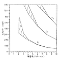
【0077】
図5は、ZnSe4分子層およびMgS2分子層を10周期繰り返したひずみ超格子内のヘビーホールの、透過率対エネルギーを示す。透過率は0.9まで高くなる。
【0078】
上述のように、青色光を生成させるためには、閉じ込めバリヤ領域のバンドギャップエネルギーを増大させることが必要である。ZnMgSSeのバンドギャップエネルギーが増大すると共に、アクセプタ濃度(Na−Nd)が急激に減少するため、伝導性が高くかつバンドギャップエネルギーが大きいZnMgSSe膜を得るのは困難である。変調ドーピングによりこれらの問題を解決し得る。しかも、本発明では、超格子の周期が十分小さいためミニバンドを形成することができ、キャリヤはミニバンドを通って移動するため(図6)、ホッピング(図2)伝導に比して良好なキャリヤ輸送(伝導)が可能となる。超格子の周期は、ミニバンドを形成するのに十分な薄さ、例えば、dを厚さとすると、dZnSe=dMgSであるとき、6分子層より少ない厚さとすべきである。
【0079】
図6は、本発明の第1の実施例を構成する半導体素子内のエネルギー準位の概略図である。この準位図は、バリヤ12によって形成される複数の量子井戸10が存在することにおいては、図2に示す図に類似する。しかし、これらには2つの顕著な相違がある。第1の相違は、ミニバンド18を有する超格子領域13が形成されるように、量子井戸10およびバリヤ12が薄くされていることである(この特徴は図示されていない)。第2の相違は、ミニバンド18へのホールの注入およびミニバンド18から素子の活性領域2へのホールの注入のための、関連するホールのエネルギー準位に関する条件が満たされているということである。ミニバンド18のエネルギーが、超格子領域13と共に本実施例のクラッド領域4からなる注入領域20のエネルギー準位と同じであるかまたはこれに十分に近い場合、ホール注入条件は満たされる。ミニバンド18の最小エネルギー準位21が、超格子領域13と素子の活性領域2との間に位置するガイド領域3の価電子帯のエネルギー準位より大きいかまたはこれと同じである場合、ホール注入条件は満たされる。これでホールは注入領域20からミニバンド18を経て活性領域2へと通過し得る。
【0080】
領域3より大きいかまたはこれに等しい、および領域20に等しいかまたはこれより小さい最小エネルギー準位を有するようなミニバンド18の形成は、超格子のバリヤ12が、素子の活性領域2より大きいバンドギャップを有する半導体材料よりなることを必要とする。ミニバンド18のエネルギーが、注入領域20のエネルギーより僅かに大きい場合でも、ホールは熱によりミニバンドの方へ注入され得る。
【0081】
図7の実施例では、ミニバンド18を有する超格子領域13は、ガイド領域3とクラッド領域4との間に組み込まれ得る。クラッド領域は、本実施例では、ホールをミニバンド18に注入する注入領域20によって形成される。LED素子では、このようなガイド領域3は省略され、超格子領域13自体が活性領域2のためのキャリヤ閉じ込めバリヤを形成する。このような場合には、ミニバンド18の最小エネルギー準位が閉じ込めバリヤのエネルギー準位に等しい。
【0082】
図8の実施例では、ミニバンド18を有する超格子領域13は、クラッド領域4内に形成される。LED素子では、ガイド領域3は省略され、クラッド領域4が活性領域2のためのキャリヤ閉じ込めバリヤを形成する。このような場合には、ミニバンド18の最小エネルギー準位は、閉じ込めバリヤのエネルギー準位に等しい。
【0083】
図9の実施例では、素子は、ミニバンド18を有する超格子領域13がガイド領域3とクラッド領域4との間に組み込まれている点において、図7の素子に類似する。しかし、本実施例では、活性領域2は、バリヤ2bによって分離される多数の量子井戸2aによって形成されるMQWからなる。ホール注入が有効に行われる条件は、ミニバンド18の最小エネルギー準位21がバリヤ2bのエネルギー準位より大きいかまたはこれに等しいことである。
【0084】
図10の実施例では、素子は、ミニバンド18を有する超格子領域13がガイド領域3とクラッド領域4との間に組み込まれている点において、図7の素子に類似する。しかし、本実施例では、超格子領域13の井戸10を形成するバルク材料のエネルギー準位は、活性領域2のエネルギー準位より小さい。
【0085】
図11は、複数のII−VI族化合物半導体のバンドギャップエネルギーおよび格子定数を示す。ZnSeおよびMgSの格子定数は、各々、5.6681Åおよび5.62Åであり、これらはGaAs基板(5.653Å)にほぼ格子整合される。ZnSeの格子定数はGaAsの格子定数より僅かに大きく、MgSの格子定数はGaAsの格子定数より僅かに小さい。従って、ZnSe−MgS超格子の内部応力は、層厚を適切に選択することによってゼロに等しくされ得る。dZnSe=2dMgSであるとき、応力はほぼ完全に相殺される。さらに、ZnSxSe1-x−MgSySe1-y(0≦x,y≦1)におけるxおよびyの適切な組成を選択することによって、超格子はGaAsに完全に格子整合し得る。また、ひずみの均衡した適当な組成物の混晶を用いると、ZnSxSe1-x−MgSySe1-y(0≦x,y≦1)超格子の内部応力はほとんどゼロに等しくなり得る。
【0086】
基板に完全い格子整合、もしくは、内部応力を超格子内でバランスさせ、ゼロに等しくすることで、高品質の超格子構造ならびに超格子部分を含む素子構造を作製することができる。
【0087】
化合物ZnSxSe1-xおよびMgSySe1-yのなかで、ZnSe(x=0)およびMgS(y=1)は2元化合物であり、従って、最も高い組成制御性を有する。また、ZnSxSe1-xおよびMgSySe1-yは、ZnMgSSe4元化合物と比較すれば大きい組成制御性を有する。
【0088】
超格子を組み込んだ素子の特性を調べるために、一連の実験を行った。
【0089】
先ず、ZnSe−MgSひずみ超格子のホトルミネセンス(PL)スペクトルのMgSバリヤ層厚依存性を調べた。ひずみ超格子を、以下の成長条件、すなわち、GaAs基板、基板温度275℃、Zn、Se、Mg、およびSのビーム等価圧力が各々6×10⁻⁷、1.4×10⁻⁶、1.0×10⁻⁷、および2×10⁻⁷Torrの条件下で、分子線エピタキシによって成長させた。
【0090】
図12は、15秒のZnSe成長時間を示し、ならびに各々、この図の12aは10秒、この図の12bは20秒、およびこの図の12cは30秒のMgS成長時間にて作製したZnSe−MgSひずみ超格子の77KでのPLスペクトルを示す。量子化エネルギー準位による発光のピークエネルギーは、各々、(a)3.19eV、(b)3.31eV、および(c)3.39eVであった。ひずみ超格子のすべてとZnSeとの間のバンドギャップエネルギー差は0.3eVより大きく、このことは、これらのひずみ超格子がクラッド領域または閉じ込めバリヤ領域として有望であることを意味する。
【0091】
第2の実験では、ZnSe−MgSひずみ超格子のPLスペクトルの、ZnSe井戸層厚依存性を調べた。ひずみ超格子を、以下の成長条件、すなわち、GaAs基板、基板温度275℃、Zn、Se、Mg、およびSのビーム等価圧力が各々8×10⁻⁷、1.8×10⁻⁶、1.0×10⁻⁷、および2×10⁻⁷Torrの条件下で、分子線エピタキシによって成長させた。
【0092】
図13は、10秒のMgS成長時間を示し、この図の13aでは10秒およびこの図の13bでは20秒のZnSe成長時間を有するZnSe−MgSひずみ超格子の77KでのPLスペクトルを示す。量子化エネルギー準位による発光のピークエネルギーは、各々、(a)3.20eVおよび(b)2.98eVであった。より薄いZnSe井戸層厚を有するひずみ超格子(図13a)とZnSeとの間のバンドギャップエネルギー差は0.3eVより大であり、これは、より薄いZnSe井戸層厚を有するひずみ超格子がクラッド領域または閉じ込めバリヤ領域としてより有望であることを意味する。
【0093】
次に、Clをドープしたひずみ超格子を成長させた。2つの異なる型のClドープひずみ超格子を図14および図15に示す。
【0094】
図14に示す素子は、n型GaAs基板30上面にn型ZnSeバッファ層32を備えている。このバッファ層32の上にアンドープZnSe−MgSひずみ超格子34が形成され、ひずみ超格子34の上にn型ZnSeキャップ層36(およびバッファ層)が形成される。これはn−i−n(ClドープZnSe、アンドープ超格子、ClドープZnSe)構造を形成する。ひずみ超格子34は、基板温度275℃、Zn、Se、Mg、およびSのビーム等価圧力が各々8×10⁻⁷、1.8×10⁻⁶、1.0×10⁻⁷、および2×10⁻⁷Torr、ならびにZnCl2のKセル温度が147℃の条件下で、分子線エピタキシによって成長させた。インジウム電極38を基板1の裏面に形成し、また半径200μmの別のインジウム電極40を真空蒸着によりキャップ層36の上に形成する。
【0095】
図15は、図14に示す素子に類似するが、アンドープZnSe−MgSひずみ超格子34がn型ZnSe−MgSひずみ超格子42に置き換わり、これにより、n−n−n(ClドープZnSe、Clドープ超格子、ClドープZnSe)構造が形成される。
【0096】
図16の16aは図13に示す素子のPLスペクトルを示す。図16の16bは図14に示す素子のPLスペクトルを示す。両素子共に、量子化エネルギー準位からの発光による3.21eVのピークエネルギーを示す。
【0097】
図17は、図14および図15に示す素子の電流−電圧特性を示す。ラインAは図14に示す素子に関し、ラインBは図15に示す素子に関する。図示するように、図15のn−n−n構造は、図14に示すn−i−n構造より良好な電流の流れを示す。これは、Clドーピングがひずみ超格子内で効率的に働くことを示している。
【0098】
窒素をドープしたひずみ超格子を有する別の2つの素子も作製した。図18に示す素子は、上部にp型ZnSeバッファ層52を形成したp型GaAs基板50を有する。層52の上にアンドープZnSe−MgSひずみ超格子34が形成され、層34の上にp型ZnSeキャップ層54が形成される。ひずみ超格子34は以下の条件、すなわち、基板温度275℃、Zn、Se、Mg、およびSのビーム等価圧力が各々8×10⁻⁷、1.8×10⁻⁶、1.0×10⁻⁷、および2×10⁻⁷Torrの条件下で、分子線エピタキシによって成長させた。これにより、p−i−p(NドープZnSe、アンドープ超格子、NドープZnSe)構造が形成される。窒素のドーピングは、入力パワー250Wおよびバックグラウンド圧力4.2×10⁻⁷Torrのラジカルなドーピング方法によって行われた。
【0099】
インジウム電極38を基板50裏面に形成し、半径200μmの金電極56をキャップ層54の上に形成する。
【0100】
図19に示す素子は、図18に示す素子に類似するが、アンドープひずみ超格子34がp型ZnSe−MgSひずみ超格子58に置き換わり、これにより、p−p−p(NドープZnSe、Nドープ超格子、NドープZnSe)構造が形成される。
【0101】
図20の20aは、図18に示す素子の77KでのPLスペクトルを示す。図20の20bは、図19に示す素子の77KでのPLスペクトルを示す。両素子共に、量子化エネルギー準位からの発光により3.21eVのピークエネルギー準位を示した。
【0102】
図21は、図18および図19に示した素子の電流−電圧特性を示す。ラインAは図18に示す素子に関し、ラインBは図19に示す素子に関する。図のように、図19に示すpドープひずみ超格子58を有する素子は、図18に示す素子に比べて、電流の流れが向上している。これは、Nドーピングがひずみ超格子内で効率的に働くことを示している。
【0103】
上記の結果は、ZnSe−MgSひずみ超格子がクラッド層またはキャリヤバリヤ層として有望であることを示す。
【0104】
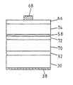
次に、図22に示すレーザは、n型GaAs基板30上部にn型ZnSeクラッド層60を備えている。n型ZnSeクラッド層60の上にはZn0.8Cd0.2Se活性層62が配置され、活性層62の上にはp型ZnSeクラッド層64が形成される。最後に、p型クラッド層64の上にp型コンタクト層66が形成される。インジウム電極38が基板30と接触して形成され、5μm幅の金電極68がp型コンタクト層66と接触して形成される。ウェハを分割し、1mmのキャビティ長を有するレーザチップを作製する。レーザはジャンクションアップの配置で銅製ヒートシンク上に取り付けられる。
【0105】
次に図23に示す第2のレーザは、図22のレーザと実質的に同一であるが、活性層62とp型ZnSeクラッド層64との間にp型ZnSe−MgSひずみ超格子58が形成される点で異なる。超格子58はミニバンドを含み、活性層62に対するキャリヤ閉じ込めバリヤを形成する。ミニバンドの最小エネルギー準位はこのバリヤのエネルギー準位に等しい。
【0106】
図22および図23のレーザの電流対光出力特性を、パルス幅が2msで1/5000デューティサイクルのパルスモードで77Kで測定した。レーザミラーはへき開端面により形成され、第2のレーザ(図23)のひずみ超格子58は、4分子層ZnSeと2分子層MgSとを20周期繰り返したものより構成された。
【0107】
これらレーザの電流対光強度特性を図24に示す。ひずみ超格子を有する第2のレーザ(図23)は10mAの閾値電流を示し、これは、ひずみ超格子のない同等のレーザの3分の1であった。これにより、ZnSe−MgSひずみ超格子は、電子のオーバフローを抑制しまた良好なホール移動を促進するのに効果的であることが分かる。レーザ発振波長は490nmであった。
【0108】
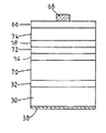
次に、図25に示す第3のレーザはn型GaAs基板30の上部にn型ZnSeバッファ層32を備えている。n型ZnSeバッファ層32の上にはn型ZnS0.07Se0.93クラッド層70が配置され、クラッド層の上にはn型ZnSe−MgSひずみ超格子42が形成される。ひずみ超格子42の上にはZnSe活性層72が形成され、活性層の上にはp型ZnSe−MgSひずみ超格子58が形成される。超格子42および58の各々は活性層72に対するキャリヤ閉じ込めバリヤを形成し、各々がミニバンドを有する。ミニバンドの最小エネルギーレベルは、バリヤのエネルギー準位に等しい。ひずみ超格子58の上にはp型ZnS0.07Se0.93クラッド層74が形成され、最後に、クラッド層74の上にp型コンタクト層66が形成される。インジウム電極38が基板30裏面に形成され、ストライプ状の電極68がコンタクト層66と接触して形成される。レーザは室温で480nmより短いレーザ発振波長を示し、これは77Kでは460nmより短い。これらレーザ発振波長はZnMgSSe4元化合物を用いることによって得ることは極めて困難である。
【0109】
次に、図26に示す第4のレーザは図25に示すレーザに類似するが、n型クラッド層70と活性層72との間に形成されたn型ZnSe−MgSひずみ超格子42が省略されている点で異なる。レーザ発振は波長445nmで77Kで観察された。
【0110】
図25および図26に示す素子では、ひずみ超格子構造は、4分子層のZnSeと2分子層のMgSとを20周期繰り返したものより構成された。
【0111】
傾斜屈折率(graded index)分離閉じ込めヘテロ構造(GRINSCH)レーザを作製した。素子は図27に示す構造を有し、図25に示す素子の構造と類似するが、活性領域72の両側のひずみ超格子42および58が、変調周期ひずみ超格子76および78に置き換えられている点で異なる。変調周期ひずみ超格子の井戸層およびバリヤ層の層厚比は、活性層の方向に変動し、これにより、図28に概略を示すように、グレーディッドなエネルギーバンドプロファイルが得られる。各超格子42および58は、活性領域72のためのキャリヤ閉じ込めバリヤを示し、ミニバンドを含む(図28には図示せず)。ミニバンドの最小エネルギー準位はバリヤのエネルギー準位に等しい。1つの変形例では、超格子は、GRINSCH構造の平坦なクラッド領域にあり、この超格子のミニバンドは、GRINSCH構造のグレーディッド領域の最小エネルギー準位に等しいかまたはこれより大きい。
【0112】
図29は、基板(図示せず)上に形成されたMg0.1ZnS0.14Seクラッド層90を有するレーザのエネルギー準位図である。層90の上に厚さ500ÅのZnS0.06Seガイド層92が形成され、さらに、厚さ50〜100ÅのCd0.2ZnSe活性層94が形成される。活性層94は、ガイド層92と同一の別のガイド層96によって覆われる。厚さ200ÅのMg0.1ZnS0.14Seクラッド層98が、ガイド層96と超格子100との間に光閉じ込め領域を提供する。クラッド層98と超格子100とがクラッド領域を形成する。このようなクラッド領域とガイド層96とは、活性層94に含まれるキャリヤのための閉じ込めバリヤとして作用する。超格子100は、厚さ5.65ÅのMgS層と厚さ11.13ÅのZnSe層とを10回繰り返したものよりなる。図29は、このような素子の伝導帯の電子および価電子帯のホールの相対エネルギー準位を示す。図29はまた、電子およびホールによって見られる、超格子100に形成された量子井戸の深さを示す。点線104および106はミニバンド107の境界を概略的に示し、ライン108は、バリヤを形成する半導体層中のアクセプタエネルギー準位を示す。
【0113】
この素子を駆動させると、電子およびホールは活性層94によって形成される量子井戸内で再結合する。ガイド層92および96は活性領域94のためのバリヤ領域を形成し、層92〜96は素子内の光ガイド層を形成する。光放射ならびに電子およびホールは、クラッド層90および98ならびに超格子100によって閉じ込められる。電子はクラッド層90に注入され、活性層94の方向に移動する。活性層94を超えて移動する電子は、点線101で示す172meVの効果的なバリヤを形成する超格子100によって反射される。ホールはヘビーホールミニバンド107に注入される。ホールは次に活性層94の方向に移動する。ホールのミニバンド107内での移動は、超格子100内の少なくともバリヤ層をドープすることによって向上する。Eaは、ドーピングによってバリヤ層に注入されたアクセプタの活性エネルギーを表す。従って、超格子100は電子を閉じ込めると共に、ホールの移動を向上させるように作用する。
【0114】
図30は、図29を参照して述べた素子に類似するレーザのエネルギー準位の図である。図30のレーザでは、超格子100が、厚さ8.47ÅのMg0.1ZnS0.14Se層と厚さ14.31ÅのMg0.4ZnS0.4Se層とを10回繰り返したものよりなるpドープ超格子102に置き換えられている。これにより、超格子のバンドギャップは図29に示す素子に較べて小さくなる。図30に示す素子の機能は図29に示す素子と同様である。
【0115】
図31は、図29および図30を参照して述べた素子に構造が類似するレーザのエネルギー準位の図である。図31のレーザでは、活性層94がIn0.2Ga0.8Nよりなる量子井戸110または多量子井戸構造に置き換えられ、ガイド領域112および114がIn0.05Ga0.95Nよりなり、またクラッド層116および118がAl0.2Ga0.8Nよりなる。超格子100は、厚さ11.4ÅのAl0.2Ga0.8N層と厚さ6.68ÅのAl0.5Ga0.5N層とを10回繰り返したpドープ超格子120に置き換えられている。図31に示す素子の機能は図29に示す素子と同様である。
【0116】
図32は、図31を参照して述べた素子に構造が類似するレーザのエネルギー準位の図である。図32のレーザでは、超格子120が、厚さ6.84ÅのGaN層と厚さ4.565ÅのAlN層とを10回繰り返したpドープ超格子122に置き換えられている。この超格子内のひずみは超格子の設計により均衡化され得る。図32に示す素子の機能は図29に示す素子と同様である。
【0117】
本発明の上記の実施例のいずれにおいても、活性層/領域は単一量子井戸構造でも多量子井戸構造でもよい。後者の場合は、ミニバンドの最小エネルギー準位は、多量子井戸構造のバリヤのエネルギー準位より大きいかまたはこれに等しい。
【0118】
ミニバンドの形成は、II−VI族半導体のみによって形成された素子に限定されない。本発明の実施例を構成する素子はまた、(AlGaIn)Pおよび(AlGaIn)N合金などのIII−V族半導体系からも形成され得る。
【0119】
従って、室温で連続動作し得る青色光レーザダイオードを提供することが可能である。
【0120】
【発明の効果】
本発明によれば、活性領域と、第1超格子領域と、該活性領域と該第1超格子領域との間に設けられるガイド領域とを有し、該第1超格子領域はバリヤ層によって互いに分離される複数の量子井戸を有する第1および第2半導体の積層パターンからなり、該パターンの積層膜厚は、該第1超格子領域内にミニバンドが形成されるように十分に薄くされる、半導体素子であって、該ミニバンドを通ってキャリヤが輸送される、半導体素子が提供される。
【0121】
この構成により、素子の活性領域の方向へのキャリアの移動を向上させることが可能となる。さらに、超格子領域はまた、傾斜屈折率領域を形成し得、これにより活性領域内の閉じ込めを向上させ得る。このようなことから、室温で連続動作し得る青色光レーザダイオードを提供することができる。
【図面の簡単な説明】
【図1】従来の分離閉じ込めヘテロ構造レーザダイオードのエネルギー準位の概略図。
【図2】 Suemune(上述)によって開示された変調ドーピング方法におけるエネルギー準位の概略図。
【図3】隣接するMgS層およびZnSe層のバンドギャップの概略図。
【図4】量子井戸内のホールのエネルギー準位、およびミニバンドを形成するための準位の拡張を示す概略図。
【図5】本発明の実施例を構成する素子の、透過率対エネルギー準位を示す図。
【図6】本発明の第1の実施例を構成する半導体素子の、キャリヤホールエネルギー準位対変位を示す概略図。
【図7】本発明の第2の実施例を構成する半導体素子の、キャリヤホールエネルギー準位対変位を示す概略図。
【図8】本発明の第3の実施例を構成する半導体素子の、キャリヤホールエネルギー準位対変位を示す概略図。
【図9】本発明の第4の実施例を構成する半導体素子の、キャリヤホールエネルギー準位対変位を示す概略図。
【図10】本発明の第5の実施例を構成する半導体素子の、キャリヤホールエネルギー準位対変位を示す概略図。
【図11】様々な半導体のバンドギャップおよび格子定数を示す図。
【図12】12a〜12cは、様々なひずみ超格子のホトルミネセンス(PL)スペクトルを示す。
【図13】13aおよび13bは、別のひずみ超格子のPLスペクトルを示す。
【図14】上記の超格子の効果を調べるための、超格子を組み込んだ素子を示す。
【図15】上記の超格子の効果を調べるための、超格子を組み込んだ素子を示す。
【図16】16aおよび16bは、図14および図15に示す素子のPLスペクトルを示す。
【図17】図14および図15に示す素子のI−V特性図。
【図18】上記の超格子の効果を調べるための、超格子を組み込んだ素子を示す。
【図19】上記の超格子の効果を調べるための、超格子を組み込んだ素子を示す。
【図20】20aおよび20bは、図18および図19に示す素子のPLスペクトルを示す。
【図21】図18および図19に示す素子のI−V特性図。
【図22】本発明の実施例を構成しないレーザを示す。
【図23】図22に示すレーザと類似するが本発明の実施例を構成するレーザを示す。
【図24】図22および図23に示す素子の、出力光強度対電流を比較する図。
【図25】本発明の別の実施例を示す。
【図26】本発明のさらに別の実施例を示す。
【図27】本発明のさらに別の実施例を示す。
【図28】図27に示す素子のエネルギー準位を示す図。
【図29】本発明のさらに別の実施例を構成するレーザのエネルギー準位を示す図。
【図30】本発明のさらに別の実施例を構成するレーザのエネルギー準位を示す図。
【図31】本発明のさらに別の実施例を構成するレーザのエネルギー準位を示す図。
【図32】本発明のさらに別の実施例を構成するレーザのエネルギー準位を示す図。
【符号の説明】
2、62、72、94 活性領域
2a、10 量子井戸
2b、12 バリヤ層
3、92、96 ガイド領域
4、64、70、74、90、98 クラッド領域
13、34、42、58、76、78、100、102 超格子領域
18、107 ミニバンド
20 注入領域[0001]
BACKGROUND OF THE INVENTION
The present invention relates to a semiconductor device having a miniband. Such a miniband improves charge movement within the device. In particular, minibands improve the characteristics of semiconductor light sources, modulators, and detectors that function in the green or blue region.
[0002]
[Prior art]
Researchers in the field of semiconductor devices continue to study semiconductor light emitting devices that provide light sources that emit blue-green light. It has been reported that II-VI group compound semiconductors have excellent characteristics as materials for the guide region and the cladding region in such a semiconductor light emitting device.
[0003]
Early studies of blue-green light emitting devices reported the use of ZnSe and ZnS 0.07 Se 0.93 as materials for the guide and cladding regions, respectively (“Blue-greeen laser diodes”, MA Haase et al., Appl. Phys. Lett. 59, 1272). It has been reported that a ZnS 0.07 Se 0.93 guide layer and a ZnMgSSe cladding layer lattice-matched to GaAs are necessary to reduce the threshold current and the laser oscillation wavelength ("Room temperature continuous operation of blue- green laser diode ", N. Nakayama et al., Electron. Lett. 29, 1488).
[0004]
[Problems to be solved by the invention]
However, the semiconductor device described above has the following problems. The band gap energy of ZnMgSSe considered to be a good material for lowering the threshold current and shortening the lasing wavelength increases and the acceptor concentration (Na—Nd) decreases rapidly. For this reason, limits have begun to appear in the threshold current and the laser oscillation wavelength. In continuous oscillation at room temperature, the shortest laser oscillation wavelength recognized by the applicant is 489 nm, and the threshold current density is 1.5 KA / cm 2 (“Continuous-wave operation of 489.9 nm blue laser diode at room temperature”, N. Nakayama et al., Electron. Lett. 29, 2164).
[0005]
In order to avoid a sharp decrease in acceptor concentration (Na—Nd) and to improve doping efficiency, it has been proposed to use a modulation doping method (“Doping in a superlattice structure: improved hole activation in wide-gap II-VI materials ", I. Suemune, J. Appl. Phys. 67, 2364). In addition, other methods of introducing superlattice structures have also been proposed ("One-hour-long room temperature CW operation of ZnMgSSe-based blue-green laser diodes", A. Ishibashi et al., 7th annual meeting on the IEEE Lasers and Electro-Optics Society (1994)).
[0006]
Even if a ZnMgSSe cladding layer lattice-matched with GaAs is used, it is considered difficult to obtain a blue laser diode having a continuous oscillation wavelength shorter than 480 nm at room temperature.
[0007]
FIG. 1 shows an energy level diagram of a conventional isolated confinement heterostructure (SCH) laser diode (LD). The
[0008]
In order to shorten the laser oscillation wavelength, it is necessary to increase the band gap energy of the
[0009]
ZnMgSSe composed of four elements is considered to be a promising material for lowering the threshold current and shortening the laser oscillation wavelength. However, as described above, it has been reported that the bandgap energy of ZnMgSSe increases and the acceptor concentration (Na—Nd) rapidly decreases. That is, it is difficult to obtain a ZnMgSSe film having good conductivity and relatively large band gap energy. ZnMgSSe having a relatively large band gap energy contains a relatively large amount of S and Mg. As a result, as the chemical composition approaches MgS, the stable crystal structure of MgS is a rock salt structure, which may result in a decrease in crystal quality as a zinc blende structure.
[0010]
It has been proposed by Suemune (described above) to use a modulation doping method to compensate for the sharp drop in acceptor concentration and to improve doping efficiency. However, in this proposal, carrier movement is performed by a mechanism known as hopping conduction, as shown in FIG.
[0011]
Modulation doping is intended to increase the free hole concentration in the valence band of the
[0012]
[Expression 1]
Because it is given by.
[0014]
Therefore, it is desirable to increase the hole concentration in order to achieve low resistance and thereby reduce power dispersion within the device. Suemune calculated that in a doped superlattice with a period of 60 Å , the free hole concentration can be increased by about 4 to 5 times. However, while holes move freely in a direction parallel to the
[0015]
European Patent Application No. 0334759 discloses a unipolar semiconductor laser having a GaAs / AlGaAs system in which the lasing structure includes internal intersubband movement between minibands within the conduction band of the semiconductor. In this device, electrons are injected into the upper subband and move laterally through the barrier region or cladding region to the active region that is part of the upper miniband. As a result of the increased energy in the barrier region of the miniband, the electron density in the active region increases, and then the electrons radiate and move to the lower miniband, thereby emitting light. The carrier exhibits coherent miniband movement through the barrier region and the active region. This element is for generating long-wavelength light and is not suitable for generating short-wavelength (green or blue) light.
[0016]
European Patent Application No. 0614253 discloses a distributed feedback (DFB) InGaAsP type laser device having an MQW laser diode section and an optical modulation section including a multi-quantum well structure integrated in the laser diode section. The multi-quantum well structure of the light modulation unit is a coupled multi-quantum well structure in which the quantum states of the quantum wells are coupled to each other to form a plurality of minibands. However, such a miniband is not involved in the movement of carriers to the active region of the laser diode portion.
[0017]
International Patent Nos. 92/08250 and 94/00884 disclose MQW photodetectors in which the quantum wells in the active region of the photodetector are separated by a superlattice barrier layer having a miniband.
[0018]
The present invention has been made to solve the above-described problems, and an object of the present invention is to provide a blue light laser diode capable of continuous operation at room temperature.
[0019]
[Means for Solving the Problems]
The semiconductor laser device of the present invention has an active region, a guide region, and a cladding region, and a superlattice region is formed in the cladding region so as to be separated from the guide region . 1 consists semiconductor and a second semiconductor stacked pattern, the first semiconductor and the second semiconductor is ing a III-V group semiconductor consisting of (AlGaIn) N, a semiconductor laser element, the guide region, The active region is configured to form a barrier, the cladding region is configured to form a barrier to the guide region, and the superlattice region includes the guide region, the superlattice region, the configured to form a barrier against the cladding region, the semiconductor laser device oscillates at a wavelength shorter than 480 nm, and the first semiconductor and the second semiconductor both between the Bandgap is characterized by greater than the bandgap of the active region, the object is achieved.
[0026]
In one embodiment, the superlattice region forms a carrier confinement barrier for the active region.
[0027]
In other embodiments, the mini-band is formed in the superlattice region and said Rukoto.
[0028]
In another embodiment, the difference between the energy of light emitted from the superlattice region in the PL spectrum and the band gap energy of the active region is greater than 0.3 eV .
[0030]
Furthermore, in another embodiment, the active region has a plurality of quantum wells separated from each other by a first barrier layer, and the minimum quantization energy level of the superlattice region is the energy of the first barrier layer. It is characterized by being greater than or equal to the level .
[0031]
Furthermore, in another embodiment, the superlattice region is characterized in that at least one of the first semiconductor and the second semiconductor is n-type doped .
[0032]
Furthermore, in another embodiment, the superlattice region is characterized in that at least one of the first semiconductor and the second semiconductor is p-type doped .
[0034]
Furthermore, in another embodiment, the semiconductor laser element is formed of a group III-V semiconductor made of (AlGaIn) N.
[0045]
According to a first aspect of the present invention, the first superlattice includes an active region, a first superlattice region, and a guide region provided between the active region and the first superlattice region. The region is composed of a stacked pattern of first and second semiconductors having a plurality of quantum wells separated from each other by a barrier layer, and the stacked film thickness of the pattern is such that a miniband is formed in the first superlattice region. A semiconductor device is provided that is sufficiently thinned so that carriers are transported through the miniband.
[0046]
According to a second aspect of the present invention, the first superlattice includes an active region, a first superlattice region, and a guide region provided between the active region and the first superlattice region. The region includes a stacked pattern of first and second semiconductors having a plurality of quantum wells separated from each other by a barrier layer, and the stacked film thickness of the pattern is such that a miniband is formed in the first superlattice region. A semiconductor device is provided that is sufficiently thinned such that the minimum energy level of the miniband is greater than or equal to the energy level or the minimum energy level of the guide region.
[0047]
According to a third aspect of the present invention, there is provided (a) an active region having a plurality of first quantum wells separated from each other by a first barrier layer, and (b) a first superlattice region, The superlattice region comprises a stacked pattern of first and second semiconductors having a plurality of second quantum wells separated from each other by a second barrier layer, and the pattern stacked film thickness is a miniband within the first superlattice region. A semiconductor device is provided, wherein the semiconductor device is thinned sufficiently such that the minimum energy level of the miniband is greater than or equal to the level of the first barrier layer. .
[0048]
As used herein, the term “miniband” means a miniband, which is a band in which charge carriers, preferably holes, can be easily moved.
[0049]
By forming a series of quantum wells in the first superlattice region at narrow intervals, the quantum wave functions extending outward from each well overlap with the wave functions of adjacent wells. Overlapping wave functions form a miniband, which improves carrier movement in the direction perpendicular to the quantum well. A superlattice is formed by successively and alternately arranging the first and second semiconductors.
[0050]
Only by injecting the carriers into the miniband can the movement of the carriers through the valence band in the first superlattice region be improved. The carrier then moves through the miniband, but may lose some energy within the miniband. The main influence on whether the carrier can move through the miniband is that the energy of the implantation region provided on the opposite side of the active region of the first superlattice region and the first superlattice region and the active region The energy of the miniband relative to the energy of the guide region or barrier between. The minimum energy of the miniband in the superlattice must be greater than or equal to the potential energy level of the guide region or barrier located between the superlattice and the active region of the device. Similarly, the energy level of the implanted region should be close to or equal to the energy level of the miniband. If the energy in the injection region is substantially lower (eg, 100 meV or more) below the minimum energy level of the miniband, carrier flow to the first superlattice region is often disturbed.
[0051]
Preferably, the semiconductor layer forming at least the barrier layer of the first superlattice region is doped. This increases the number of carriers and improves the conductivity in the first superlattice region. The quantum well region of the first superlattice can also be doped.
[0052]
Preferably, the width of the miniband is selected to substantially maximize carrier movement. Preferably, the carrier is a hole. The width of the miniband depends on the semiconductor material and on the widths of the barrier and well layers, ie the widths of the first and second semiconductors. In addition, the width of the miniband is such that carriers can move through the miniband even when an electric field is formed across the first region, i.e. the miniband does not separate into the Stark level. Selected.
[0053]
Preferably, the semiconductor is selected from a quaternary mixed crystal composed of Zn, Mg, S, and Se. The first and second regions, it is convenient to form a superlattice having a ZnS x Se 1-x -MgS y Se 1-y (0 ≦ x, y ≦ 1) structure.
[0054]
Conveniently, the band gap may be varied by changing the width of each of the first and second semiconductors or the stacked film thickness of the pattern. The band gap can vary substantially in the shape of a parabola. The second superlattice region may be disposed on the opposite side of the active region from the first superlattice region. The superlattice regions each have a layer thickness that varies spatially, and can cooperate to form a graded-index separated confinement heterostructure element. Such a structure is optically efficient.
[0055]
Preferably, the first and second semiconductors are substantially lattice matched with the lattice of the substrate such that little or no stress is applied to the first and second semiconductor layers. The substrate can be GaAs and the lattice constants of the first and second semiconductor layers can be varied by changing the concentration of Mg and / or S in the layers.
[0056]
Preferably, the element is an LED, laser, modulator, or detector.
[0057]
As a variant, the first and second semiconductors may be formed from III-V semiconductor systems such as (AlGaIn) P and (AlGaIn) N alloys.
[0058]
Periodic lamination is preferably 6 molecular layers or less. In the case of a material having a zinc blende structure, the molecular layer thickness is half of the lattice constant.
[0059]
Therefore, it is possible to improve the movement of carriers in the direction of the active region of the element. Furthermore, the superlattice region can also form a gradient index region, thereby improving confinement in the active region.
[0060]
DETAILED DESCRIPTION OF THE INVENTION
As described above, it is necessary to increase the band gap energy of the confinement barrier formed by the guide region or barrier and cladding region of the semiconductor laser, thereby reducing the threshold current and shortening the laser oscillation wavelength. It is possible to increase the band gap by changing the ratio of S and Mg in ZnMgSSe, but this requires a very large amount of S and Mg, so that the crystal structure is similar to MgS . As a result, since the stable crystal structure of MgS is a rock salt structure, the crystal quality deteriorates. Therefore, from the viewpoint of crystal quality, the composition of S and Mg in ZnMgSSe has an upper limit. However, this upper limit can be negated by growing a MgS film having a zinc blende structure rather than a rock salt structure by using a superlattice structure. If the film thickness of MgS y Se 1-y (0 ≦ y ≦ 1) is sufficiently thin, MgS y Se 1-y having a zinc blende structure is deposited on ZnS x Se 1-x (0 ≦ x ≦ 1). resulting grown, also be grown upper ZnS x Se 1-x layer on MgS y Se 1-y layer, zinc blende structure of MgS y Se 1-y layer will stabilize. These layers are formed by lamination, and due to band discontinuity between layers, as shown in FIG. 3, the theoretical maximum band discontinuity value, ΔEc (conduction band energy change) is 0 to 1115 meV, and ΔEv (valence electrons). A superlattice having a band energy change) of 0 to 736 meV can be formed. FIG. 3 shows two energy levels in the valence band. These levels are associated with light holes (lh) and heavy holes (hh).
[0061]
In a structure having first and second semiconductor layers alternately stacked, a miniband is formed when the layer thickness is reduced. The formation of minibands can be thought of as a superposition of multiple solutions to quantum mechanics problems known as “rectangular wells” or “particles in a box”. In summary, the problem of “rectangular wells” is that for an infinitely deep well of width Lz (extending from 0 to Lz), the Schrodinger equation,
[0062]
[Expression 2]
Means to solve. In this solution, as a boundary condition, the wave function is zero at the end of the well. Therefore, the solution is
[0064]
[Equation 3]
Given in. Where m is the effective mass of the particle, h is the Planck constant / 2π, ψ is the quantum wave function, and Z is the position in the box.
[Expression 4]
It is.
[0068]
However, if the well height is finite, the wave function can take a non-zero value outside the well confinement. In addition, this solution includes both even (symmetric) and odd (asymmetric) solutions.
[0069]
The solution by the finite well equation for a well extending from -L / 2 to + L / 2 is in the well
[Equation 5]
An even solution approximating to and in the well
[Formula 6]
Gives an asymmetric solution approximating. Each solution also has a damped wave that extends outside the well.
[0074]
The energy level of a finite rectangular well is similar to the corresponding level of an infinitely deep well solution, but slightly lower.
[0075]
FIG. 4 shows the first three energy levels of holes in a finite well (E 1 , E 2 in this figure), which is one of a series of wells formed by alternately stacking ZnSe and MgS layers. , The three energy levels of E 3 ). The thickness is measured by the molecular layer thickness of the crystal (the thickness of one molecular layer is approximately equal to 2.82 Å ). The thickness of the well and barrier is substantially the same.
[0076]
Each well is effectively separated from an adjacent well when the well and barrier layers are thick and the value of the damped wave function from the adjacent well is substantially zero. By reducing the well and barrier widths, the energy level of the solution increases, as can be expected since En is inversely proportional to the well width. As the well and barrier widths are further reduced, the damped wave functions of the other wells (the symmetric and asymmetric solutions thereof have different values) begin to have significant non-zero values in the wells, thereby causing energy levels The solution is divided into a series of values. As a result of the formation of a series of quantum wells, the energy levels form a continuum within the band, as shown by the shaded region in FIG.
[0077]
FIG. 5 shows the transmittance versus energy of a heavy hole in a strained superlattice in which a ZnSe4 molecular layer and an MgS2 molecular layer are repeated for 10 periods. The transmittance increases to 0.9.
[0078]
As described above, in order to generate blue light, it is necessary to increase the band gap energy of the confinement barrier region. As the band gap energy of ZnMgSSe increases and the acceptor concentration (Na—Nd) decreases rapidly, it is difficult to obtain a ZnMgSSe film with high conductivity and large band gap energy. Modulation doping can solve these problems. Moreover, in the present invention, since the period of the superlattice is sufficiently small, a miniband can be formed, and the carrier moves through the miniband (FIG. 6), which is better than hopping (FIG. 2) conduction. Carrier transport (conduction) is possible. The period of the superlattice should be thin enough to form a miniband, eg less than 6 molecular layers when d ZnSe = d MgS, where d is thick.
[0079]
FIG. 6 is a schematic diagram of energy levels in the semiconductor element constituting the first embodiment of the present invention. This level diagram is similar to the diagram shown in FIG. 2 in that there are a plurality of
[0080]
Formation of the
[0081]
In the embodiment of FIG. 7, the
[0082]
In the embodiment of FIG. 8, the
[0083]
In the embodiment of FIG. 9, the device is similar to the device of FIG. 7 in that a
[0084]
In the embodiment of FIG. 10, the device is similar to the device of FIG. 7 in that a
[0085]
FIG. 11 shows band gap energies and lattice constants of a plurality of II-VI group compound semiconductors. Lattice constants of ZnSe and MgS are each a 5.6681 Å and 5.62 Å, which are almost lattice matched to a GaAs substrate (5.653 Å). The lattice constant of ZnSe is slightly larger than that of GaAs, and the lattice constant of MgS is slightly smaller than that of GaAs. Thus, the internal stress of the ZnSe-MgS superlattice can be made equal to zero by appropriately selecting the layer thickness. When d ZnSe = 2d MgS , the stress is almost completely offset. Further, ZnS x Se 1-x -MgS y Se 1-y (0 ≦ x, y ≦ 1) by selecting the appropriate composition of x and y in the superlattice may perfectly lattice matched to GaAs. Moreover, the use of mixed crystals of suitable composition balance of the strain, ZnS x Se 1-x -MgS y Se 1-y (0 ≦ x, y ≦ 1) internal stress of the superlattice becomes almost equal to zero obtain.
[0086]
By perfect lattice matching to the substrate, or by balancing the internal stress within the superlattice and making it equal to zero, a high-quality superlattice structure and a device structure including a superlattice portion can be fabricated.
[0087]
Among the compounds ZnS x Se 1-x and MgS y Se 1-y , ZnSe (x = 0) and MgS (y = 1) are binary compounds and therefore have the highest composition controllability. In addition, ZnS x Se 1-x and MgS y Se 1-y have greater composition controllability than the ZnMgSSe quaternary compound.
[0088]
A series of experiments were conducted to investigate the characteristics of devices incorporating superlattices.
[0089]
First, the MgS barrier layer thickness dependence of the photoluminescence (PL) spectrum of a ZnSe-MgS strained superlattice was investigated. The strained superlattice is grown under the following growth conditions: GaAs substrate, substrate temperature 275 ° C., beam equivalent pressures of Zn, Se, Mg, and S are 6 × 10 −7 , 1.4 × 10 −6 , respectively. Growth was performed by molecular beam epitaxy under conditions of 0 × 10 −7 and 2 × 10 −7 Torr.
[0090]
FIG. 12 shows a ZnSe growth time of 15 seconds and, respectively, 12a in this figure is 10 seconds, 12b in this figure is 20 seconds, and 12c in this figure is a ZnSe− produced with an MgS growth time of 30 seconds. The PL spectrum at 77K of the MgS strained superlattice is shown. The peak energies of light emission due to the quantization energy level were (a) 3.19 eV, (b) 3.31 eV, and (c) 3.39 eV, respectively. The band gap energy difference between all of the strained superlattices and ZnSe is greater than 0.3 eV, which means that these strained superlattices are promising as cladding or confinement barrier regions.
[0091]
In the second experiment, the dependence of the PL spectrum of the ZnSe-MgS strained superlattice on the ZnSe well layer thickness was examined. The strained superlattice is grown under the following growth conditions: GaAs substrate, substrate temperature 275 ° C., beam equivalent pressures of Zn, Se, Mg, and S are 8 × 10 −7 , 1.8 × 10 −6 , respectively. Growth was performed by molecular beam epitaxy under conditions of 0 × 10 −7 and 2 × 10 −7 Torr.
[0092]
FIG. 13 shows the MgS growth time of 10 seconds, the PL spectrum at 77K of a ZnSe—MgS strained superlattice with a ZnSe growth time of 10 seconds in FIG. 13a and 20 seconds in FIG. The peak energy of light emission by the quantization energy level was (a) 3.20 eV and (b) 2.98 eV, respectively. The band gap energy difference between the strained superlattice with the thinner ZnSe well layer thickness (FIG. 13a) and ZnSe is greater than 0.3 eV, which is the same as the strained superlattice with the thinner ZnSe well layer thickness clad. It means more promising as a region or confinement barrier region.
[0093]
Next, a strained superlattice doped with Cl was grown. Two different types of Cl-doped strained superlattices are shown in FIGS.
[0094]
The element shown in FIG. 14 includes an n-type
[0095]
FIG. 15 is similar to the device shown in FIG. 14 except that the undoped ZnSe—MgS
[0096]
16a of FIG. 16 shows the PL spectrum of the element shown in FIG. 16b of FIG. 16 shows the PL spectrum of the element shown in FIG. Both elements show a peak energy of 3.21 eV due to light emission from the quantization energy level.
[0097]
FIG. 17 shows current-voltage characteristics of the elements shown in FIGS. Line A relates to the element shown in FIG. 14, and line B relates to the element shown in FIG. As shown, the nn structure of FIG. 15 shows a better current flow than the nn structure shown in FIG. This indicates that Cl doping works efficiently in the strained superlattice.
[0098]
Two other devices with strained superlattices doped with nitrogen were also fabricated. The element shown in FIG. 18 has a p-
[0099]
An
[0100]
The device shown in FIG. 19 is similar to the device shown in FIG. 18 except that the undoped
[0101]
20a of FIG. 20 shows the PL spectrum at 77K of the element shown in FIG. 20b of FIG. 20 shows the PL spectrum at 77K of the element shown in FIG. Both devices showed a peak energy level of 3.21 eV by light emission from the quantization energy level.
[0102]
FIG. 21 shows current-voltage characteristics of the elements shown in FIGS. Line A relates to the element shown in FIG. 18, and line B relates to the element shown in FIG. As shown, the element having the p-doped
[0103]
The above results indicate that ZnSe-MgS strained superlattices are promising as cladding layers or carrier barrier layers.
[0104]
Next, the laser shown in FIG. 22 includes an n-type
[0105]
Next, the second laser shown in FIG. 23 is substantially the same as the laser shown in FIG. 22, but a p-type ZnSe—MgS
[0106]
The current versus light output characteristics of the lasers of FIGS. 22 and 23 were measured at 77K in a pulse mode with a pulse width of 2 ms and a 1/5000 duty cycle. The laser mirror was formed by a cleaved end face, and the
[0107]
The current vs. light intensity characteristics of these lasers are shown in FIG. A second laser with a strained superlattice (FIG. 23) showed a threshold current of 10 mA, which was one third of an equivalent laser without a strained superlattice. Thus, it can be seen that the ZnSe—MgS strained superlattice is effective in suppressing electron overflow and promoting good hole movement. The laser oscillation wavelength was 490 nm.
[0108]
Next, the third laser shown in FIG. 25 includes an n-type
[0109]
Next, the fourth laser shown in FIG. 26 is similar to the laser shown in FIG. 25 except that the n-type ZnSe—MgS
[0110]
In the element shown in FIGS. 25 and 26, the strained superlattice structure is composed of 20 cycles of a tetramolecular layer of ZnSe and a bimolecular layer of MgS.
[0111]
A graded index separate confinement heterostructure (GRINSCH) laser was fabricated. The device has the structure shown in FIG. 27 and is similar to the structure of the device shown in FIG. 25, except that the
[0112]
FIG. 29 is an energy level diagram of a laser having an Mg 0.1 ZnS 0.14
[0113]
When this device is driven, electrons and holes recombine in the quantum well formed by the
[0114]
FIG. 30 is a diagram of the energy levels of a laser similar to the device described with reference to FIG. In the laser of FIG. 30, the
[0115]
FIG. 31 is a diagram of the energy levels of a laser whose structure is similar to the device described with reference to FIGS. In the laser of FIG. 31, the
[0116]
FIG. 32 is a diagram of the energy levels of a laser whose structure is similar to the device described with reference to FIG. In the laser of FIG. 32, the
[0117]
In any of the above embodiments of the present invention, the active layer / region may be a single quantum well structure or a multi-quantum well structure. In the latter case, the minimum energy level of the miniband is greater than or equal to the energy level of the barrier of the multi-quantum well structure.
[0118]
The formation of the miniband is not limited to an element formed only by a II-VI group semiconductor. Devices constituting embodiments of the present invention can also be formed from III-V semiconductor systems such as (AlGaIn) P and (AlGaIn) N alloys.
[0119]
Therefore, it is possible to provide a blue light laser diode that can operate continuously at room temperature.
[0120]
【The invention's effect】
According to the present invention, there is provided an active region, a first superlattice region, and a guide region provided between the active region and the first superlattice region, and the first superlattice region is formed by a barrier layer. It consists of a stacked pattern of first and second semiconductors having a plurality of quantum wells separated from each other, and the stacked film thickness of the pattern is made sufficiently thin so that a miniband is formed in the first superlattice region. A semiconductor device is provided wherein carriers are transported through the miniband.
[0121]
With this configuration, it is possible to improve the movement of carriers in the direction of the active region of the element. Furthermore, the superlattice region can also form a gradient index region, thereby improving confinement in the active region. Therefore, a blue light laser diode that can continuously operate at room temperature can be provided.
[Brief description of the drawings]
FIG. 1 is a schematic diagram of energy levels of a conventional separately confined heterostructure laser diode.
FIG. 2 is a schematic diagram of energy levels in the modulation doping method disclosed by Suemune (supra).
FIG. 3 is a schematic diagram of band gaps of adjacent MgS layers and ZnSe layers.
FIG. 4 is a schematic diagram showing the energy levels of holes in a quantum well and the level expansion to form a miniband.
FIG. 5 is a diagram showing transmittance versus energy level of an element constituting an embodiment of the present invention.
FIG. 6 is a schematic diagram showing carrier hole energy level versus displacement of the semiconductor device constituting the first embodiment of the present invention.
FIG. 7 is a schematic view showing carrier hole energy level versus displacement of a semiconductor device constituting a second embodiment of the present invention.
FIG. 8 is a schematic diagram showing carrier hole energy level versus displacement of a semiconductor device constituting a third embodiment of the present invention.
FIG. 9 is a schematic view showing carrier hole energy level versus displacement of a semiconductor device constituting a fourth embodiment of the present invention.
FIG. 10 is a schematic view showing carrier hole energy level versus displacement of a semiconductor device constituting a fifth embodiment of the present invention.
FIG. 11 shows band gaps and lattice constants of various semiconductors.
FIGS. 12a-12c show the photoluminescence (PL) spectra of various strained superlattices.
13a and 13b show the PL spectra of another strained superlattice.
FIG. 14 shows a device incorporating a superlattice for examining the effect of the superlattice.
FIG. 15 shows an element incorporating a superlattice for examining the effect of the superlattice.
16a and 16b show PL spectra of the elements shown in FIGS. 14 and 15. FIG.
17 is an IV characteristic diagram of the element shown in FIGS. 14 and 15. FIG.
FIG. 18 shows a device incorporating a superlattice for examining the effect of the superlattice.
FIG. 19 shows a device incorporating a superlattice for examining the effect of the superlattice.
20a and 20b show the PL spectra of the device shown in FIGS. 18 and 19. FIG.
21 is an IV characteristic diagram of the element shown in FIGS. 18 and 19. FIG.
FIG. 22 shows a laser that does not constitute an embodiment of the present invention.
FIG. 23 shows a laser similar to the laser shown in FIG. 22 but constituting an embodiment of the present invention.
24 is a graph comparing output light intensity versus current for the elements shown in FIGS. 22 and 23. FIG.
FIG. 25 shows another embodiment of the present invention.
FIG. 26 shows still another embodiment of the present invention.
FIG. 27 shows yet another embodiment of the present invention.
FIG. 28 is a diagram showing energy levels of the element shown in FIG.
FIG. 29 is a diagram showing the energy level of a laser constituting still another embodiment of the present invention.
FIG. 30 is a diagram showing the energy level of a laser constituting still another embodiment of the present invention.
FIG. 31 is a diagram showing the energy level of a laser constituting still another embodiment of the present invention.
FIG. 32 is a diagram showing the energy level of a laser constituting still another embodiment of the present invention.
[Explanation of symbols]
2, 62, 72, 94
Claims (7)
該ガイド領域は、該活性領域に対してバリヤを形成するように構成され、
該クラッド領域は、該ガイド領域に対してバリヤを形成するように構成され、
該超格子領域は、該ガイド領域と該超格子領域との間の該クラッド領域に対してバリヤを形成するように構成され、
該半導体レーザ素子は480nmより短い波長で発振し、かつ、
該第1半導体および該第2半導体の両方のバンドギャップが該活性領域のバンドギャップより大きいことを特徴とする、半導体レーザ素子。An active region, a guide region, and a cladding region are formed, and a superlattice region is formed in the cladding region so as to be separated from the guide region , and the superlattice region includes at least a stack of a first semiconductor and a second semiconductor consists pattern, the first semiconductor and the second semiconductor is ing a III-V group semiconductor consisting of (AlGaIn) N, a semiconductor laser element,
The guide region is configured to form a barrier to the active region;
The cladding region is configured to form a barrier to the guide region;
The superlattice region is configured to form a barrier to the cladding region between the guide region and the superlattice region;
The semiconductor laser element oscillates at a wavelength shorter than 480 nm, and
A semiconductor laser device, wherein a band gap of both the first semiconductor and the second semiconductor is larger than a band gap of the active region.
Applications Claiming Priority (2)
| Application Number | Priority Date | Filing Date | Title |
|---|---|---|---|
| GB9504666A GB2298735A (en) | 1995-03-08 | 1995-03-08 | Semiconductor device having a miniband |
| GB9504666.0 | 1995-03-08 |
Related Child Applications (2)
| Application Number | Title | Priority Date | Filing Date |
|---|---|---|---|
| JP2004190448A Division JP4067104B2 (en) | 1995-03-08 | 2004-06-28 | Semiconductor device having a miniband |
| JP2006348527A Division JP4153966B2 (en) | 1995-03-08 | 2006-12-25 | Semiconductor light emitting device |
Publications (2)
| Publication Number | Publication Date |
|---|---|
| JPH08250810A JPH08250810A (en) | 1996-09-27 |
| JP3909884B2 true JP3909884B2 (en) | 2007-04-25 |
Family
ID=10770858
Family Applications (4)
| Application Number | Title | Priority Date | Filing Date |
|---|---|---|---|
| JP05213596A Expired - Fee Related JP3909884B2 (en) | 1995-03-08 | 1996-03-08 | Semiconductor laser element |
| JP2004190448A Expired - Fee Related JP4067104B2 (en) | 1995-03-08 | 2004-06-28 | Semiconductor device having a miniband |
| JP2006348527A Expired - Fee Related JP4153966B2 (en) | 1995-03-08 | 2006-12-25 | Semiconductor light emitting device |
| JP2007232324A Expired - Fee Related JP4685845B2 (en) | 1995-03-08 | 2007-09-07 | Semiconductor light emitting device |
Family Applications After (3)
| Application Number | Title | Priority Date | Filing Date |
|---|---|---|---|
| JP2004190448A Expired - Fee Related JP4067104B2 (en) | 1995-03-08 | 2004-06-28 | Semiconductor device having a miniband |
| JP2006348527A Expired - Fee Related JP4153966B2 (en) | 1995-03-08 | 2006-12-25 | Semiconductor light emitting device |
| JP2007232324A Expired - Fee Related JP4685845B2 (en) | 1995-03-08 | 2007-09-07 | Semiconductor light emitting device |
Country Status (5)
| Country | Link |
|---|---|
| US (1) | US5747827A (en) |
| EP (2) | EP0731510B1 (en) |
| JP (4) | JP3909884B2 (en) |
| DE (1) | DE69636110T2 (en) |
| GB (1) | GB2298735A (en) |
Families Citing this family (32)
| Publication number | Priority date | Publication date | Assignee | Title |
|---|---|---|---|---|
| JP3478090B2 (en) * | 1997-05-26 | 2003-12-10 | 日亜化学工業株式会社 | Nitride semiconductor device |
| US6677619B1 (en) | 1997-01-09 | 2004-01-13 | Nichia Chemical Industries, Ltd. | Nitride semiconductor device |
| WO1998031055A1 (en) * | 1997-01-09 | 1998-07-16 | Nichia Chemical Industries, Ltd. | Nitride semiconductor device |
| JPH1146038A (en) * | 1997-05-29 | 1999-02-16 | Nichia Chem Ind Ltd | Nitride semiconductor laser element and manufacture of the same |
| CN1142598C (en) * | 1997-07-25 | 2004-03-17 | 日亚化学工业株式会社 | Nitride semiconductor device |
| US6459096B1 (en) * | 1998-01-14 | 2002-10-01 | Manijeh Razeghi | Multi quantum well grinsch detector |
| KR100611352B1 (en) | 1998-03-12 | 2006-09-27 | 니치아 카가쿠 고교 가부시키가이샤 | Nitride semiconductor device |
| DE19824222A1 (en) * | 1998-05-29 | 1999-12-02 | Lite On Electronics Inc | Transparent window layer for light emitting diode |
| GB9913950D0 (en) | 1999-06-15 | 1999-08-18 | Arima Optoelectronics Corp | Unipolar light emitting devices based on iii-nitride semiconductor superlattices |
| DE19955747A1 (en) | 1999-11-19 | 2001-05-23 | Osram Opto Semiconductors Gmbh | Optical semiconductor device with multiple quantum well structure, e.g. LED, has alternate well layers and barrier layers forming super-lattices |
| JP4854829B2 (en) * | 1999-11-22 | 2012-01-18 | 日亜化学工業株式会社 | Nitride semiconductor laser device |
| JP4547765B2 (en) * | 2000-03-30 | 2010-09-22 | 三菱電機株式会社 | Optical modulator, semiconductor laser device with optical modulator, and optical communication device |
| US6891187B2 (en) * | 2001-08-17 | 2005-05-10 | Lucent Technologies Inc. | Optical devices with heavily doped multiple quantum wells |
| US6711195B2 (en) * | 2002-02-28 | 2004-03-23 | Agilent Technologies, Inc. | Long-wavelength photonic device with GaAsSb quantum-well layer |
| US7042921B2 (en) | 2003-07-11 | 2006-05-09 | Emcore Corporation | Complex coupled single mode laser with dual active region |
| NO20041523L (en) * | 2003-09-19 | 2005-03-21 | Sumitomo Electric Industries | Light emitting semiconductor element |
| GB2410848A (en) | 2004-02-05 | 2005-08-10 | Dyson Ltd | Voltage compensation in switched reluctance motor |
| GB2410847A (en) | 2004-02-05 | 2005-08-10 | Dyson Ltd | Control of motor winding energisation according to rotor angle |
| US7098471B2 (en) * | 2004-06-14 | 2006-08-29 | Avago Technologies Fiber Ip (Singapore) Pte. Ltd. | Semiconductor quantum well devices and methods of making the same |
| KR100670531B1 (en) * | 2004-08-26 | 2007-01-16 | 엘지이노텍 주식회사 | Nitride semiconductor LED and fabrication method thereof |
| KR100718129B1 (en) * | 2005-06-03 | 2007-05-14 | 삼성전자주식회사 | ?-? group GaN-based compound semiconductor device |
| JP4920221B2 (en) * | 2005-09-05 | 2012-04-18 | 学校法人上智学院 | Optical semiconductor device having InP substrate |
| DE102007044439B4 (en) * | 2007-09-18 | 2022-03-24 | OSRAM Opto Semiconductors Gesellschaft mit beschränkter Haftung | Optoelectronic semiconductor chip with a quantum well structure |
| KR100887050B1 (en) | 2007-12-06 | 2009-03-04 | 삼성전기주식회사 | Nitride semiconductor device |
| TWI427824B (en) * | 2008-03-14 | 2014-02-21 | Asahi Kasei Emd Corp | Infrared ray emitting element |
| KR101018088B1 (en) * | 2008-11-07 | 2011-02-25 | 삼성엘이디 주식회사 | Nitride Semiconductor Device |
| JP4681684B1 (en) * | 2009-08-24 | 2011-05-11 | Dowaエレクトロニクス株式会社 | Nitride semiconductor device and manufacturing method thereof |
| TWI557936B (en) | 2010-04-30 | 2016-11-11 | 美國波士頓大學信託會 | High efficiency ultraviolet light emitting diode with band structure potential fluctuations |
| US8723189B1 (en) | 2012-01-06 | 2014-05-13 | Trustees Of Boston University | Ultraviolet light emitting diode structures and methods of manufacturing the same |
| CN103413877B (en) * | 2013-08-16 | 2016-01-20 | 湘能华磊光电股份有限公司 | The growing method of epitaxial structure quantum well stress release layer and epitaxial structure thereof |
| JP2015207584A (en) * | 2014-04-17 | 2015-11-19 | 浜松ホトニクス株式会社 | semiconductor laser |
| JP2017069299A (en) | 2015-09-29 | 2017-04-06 | 豊田合成株式会社 | Group iii nitride semiconductor light-emitting element |
Family Cites Families (23)
| Publication number | Priority date | Publication date | Assignee | Title |
|---|---|---|---|---|
| JPS6028268A (en) * | 1983-07-26 | 1985-02-13 | Agency Of Ind Science & Technol | Semiconductor device |
| US4866488A (en) * | 1985-03-29 | 1989-09-12 | Texas Instruments Incorporated | Ballistic transport filter and device |
| US4731789A (en) * | 1985-05-13 | 1988-03-15 | Xerox Corporation | Clad superlattice semiconductor laser |
| JPH0634425B2 (en) * | 1986-07-25 | 1994-05-02 | 三菱電機株式会社 | Semiconductor laser |
| US4882734A (en) * | 1988-03-09 | 1989-11-21 | Xerox Corporation | Quantum well heterostructure lasers with low current density threshold and higher TO values |
| JPH01241192A (en) * | 1988-03-23 | 1989-09-26 | Fujitsu Ltd | Semiconductor device |
| US4862471A (en) * | 1988-04-22 | 1989-08-29 | University Of Colorado Foundation, Inc. | Semiconductor light emitting device |
| JP2653471B2 (en) * | 1988-05-24 | 1997-09-17 | 日本電信電話株式会社 | Semiconductor device |
| JPH01298786A (en) * | 1988-05-26 | 1989-12-01 | Sharp Corp | Semiconductor laser device and manufacture thereof |
| JPH08111541A (en) * | 1989-12-08 | 1996-04-30 | Hitachi Ltd | Semiconductor device |
| JPH03257887A (en) * | 1990-03-07 | 1991-11-18 | Fuji Xerox Co Ltd | Semiconductor laser device |
| US5040186A (en) * | 1990-03-13 | 1991-08-13 | At&T Bell Laboratories | InP-based quantum-well laser |
| CA2091053A1 (en) * | 1990-10-31 | 1992-05-01 | John W. Little, Jr. | Miniband transport quantum well infrared detector |
| JP3398966B2 (en) * | 1991-02-21 | 2003-04-21 | ソニー株式会社 | Semiconductor light emitting device |
| EP0556461B1 (en) * | 1992-02-19 | 1998-01-14 | Sony Corporation | Semiconductor laser |
| JP3245937B2 (en) * | 1992-03-25 | 2002-01-15 | ソニー株式会社 | Semiconductor light emitting device |
| IL106130A (en) * | 1992-06-30 | 1996-10-19 | Martin Marietta Corp | Semiconductor miniband transport quantum well detector and a method for detecting electromagnetic radiation |
| JP3198678B2 (en) * | 1992-10-29 | 2001-08-13 | 豊田合成株式会社 | Nitrogen-3 group element compound semiconductor light emitting device |
| JP2536714B2 (en) * | 1993-03-03 | 1996-09-18 | 日本電気株式会社 | Optical modulator integrated multiple quantum well semiconductor laser device |
| JP3243111B2 (en) * | 1993-03-15 | 2002-01-07 | 株式会社東芝 | Compound semiconductor device |
| JPH0715085A (en) * | 1993-06-25 | 1995-01-17 | Furukawa Electric Co Ltd:The | Semiconductor laser element |
| MY111898A (en) * | 1993-07-02 | 2001-02-28 | Sony Corp | Semiconductor laser |
| JP3116675B2 (en) * | 1993-07-28 | 2000-12-11 | ソニー株式会社 | Semiconductor laser |
-
1995
- 1995-03-08 GB GB9504666A patent/GB2298735A/en not_active Withdrawn
-
1996
- 1996-03-07 US US08/612,294 patent/US5747827A/en not_active Expired - Lifetime
- 1996-03-08 EP EP96301594A patent/EP0731510B1/en not_active Expired - Lifetime
- 1996-03-08 JP JP05213596A patent/JP3909884B2/en not_active Expired - Fee Related
- 1996-03-08 EP EP01204026A patent/EP1213771A3/en not_active Withdrawn
- 1996-03-08 DE DE69636110T patent/DE69636110T2/en not_active Expired - Lifetime
-
2004
- 2004-06-28 JP JP2004190448A patent/JP4067104B2/en not_active Expired - Fee Related
-
2006
- 2006-12-25 JP JP2006348527A patent/JP4153966B2/en not_active Expired - Fee Related
-
2007
- 2007-09-07 JP JP2007232324A patent/JP4685845B2/en not_active Expired - Fee Related
Also Published As
| Publication number | Publication date |
|---|---|
| DE69636110D1 (en) | 2006-06-14 |
| EP0731510B1 (en) | 2006-05-10 |
| JPH08250810A (en) | 1996-09-27 |
| JP2007324628A (en) | 2007-12-13 |
| EP1213771A2 (en) | 2002-06-12 |
| DE69636110T2 (en) | 2007-04-19 |
| JP2004274089A (en) | 2004-09-30 |
| JP4685845B2 (en) | 2011-05-18 |
| GB9504666D0 (en) | 1995-04-26 |
| EP0731510A3 (en) | 1997-01-15 |
| US5747827A (en) | 1998-05-05 |
| EP0731510A2 (en) | 1996-09-11 |
| GB2298735A (en) | 1996-09-11 |
| JP2007081449A (en) | 2007-03-29 |
| JP4067104B2 (en) | 2008-03-26 |
| EP1213771A3 (en) | 2002-10-02 |
| JP4153966B2 (en) | 2008-09-24 |
Similar Documents
| Publication | Publication Date | Title |
|---|---|---|
| JP4153966B2 (en) | Semiconductor light emitting device | |
| Gaines et al. | Blue‐green injection lasers containing pseudomorphic Zn1− x Mg x S y Se1− y cladding layers and operating up to 394 K | |
| US5538918A (en) | Method of fabricating a buried-ridge II-VI laser diode | |
| JP4138930B2 (en) | Quantum semiconductor device and quantum semiconductor light emitting device | |
| US6859477B2 (en) | Optoelectronic and electronic devices based on quantum dots having proximity-placed acceptor impurities, and methods therefor | |
| US20020079485A1 (en) | Quantum dash device | |
| JP2004537854A (en) | Combined quantum dot and quantum well semiconductor device and device forming method | |
| EP2686924A2 (en) | Lasers with quantum wells having high indium and low aluminum with barrier layers having high aluminum and low indium with reduced traps | |
| JP5575253B2 (en) | Tunable quantum light source | |
| Anders et al. | Electroluminescence of a quantum dot cascade structure | |
| US5473173A (en) | Quantum well structure having differentially strained quantum well layers | |
| JP4996869B2 (en) | Semiconductor laser | |
| US6859474B1 (en) | Long wavelength pseudomorphic InGaNPAsSb type-I and type-II active layers for the gaas material system | |
| WO2010022526A2 (en) | Superluminescent diode, or amplifier chip | |
| US5362974A (en) | Group II-VI material semiconductor optical device with strained multiquantum barriers | |
| US7668217B2 (en) | Semiconductor laser diode device | |
| Choi et al. | Antimonide-based mid-infrared lasers | |
| Meyer et al. | Reduced-dimensionality HgTe-CdTe for the infrared | |
| JP2570732B2 (en) | Semiconductor laser | |
| GB2488199A (en) | A tuneable quantum light source which mimimizes fine structure splitting (FSS) | |
| JPH07326824A (en) | Light-emitting element | |
| Gunshor et al. | II–VI semiconductors come of age | |
| Lebedev et al. | Electrical and Optical Studies of Tunneling Transport Phenomena in Zn (Cd) Se/Zn (Mg) SSe Quantum Well and Superlattice Structures | |
| Voss et al. | Basic physics of semiconductor laser | |
| Kurtz et al. | Infrared emitting device and method |
Legal Events
| Date | Code | Title | Description |
|---|---|---|---|
| A975 | Report on accelerated examination |
Free format text: JAPANESE INTERMEDIATE CODE: A971005 Effective date: 20040108 |
|
| A131 | Notification of reasons for refusal |
Free format text: JAPANESE INTERMEDIATE CODE: A131 Effective date: 20040121 |
|
| A521 | Written amendment |
Free format text: JAPANESE INTERMEDIATE CODE: A523 Effective date: 20040322 |
|
| A02 | Decision of refusal |
Free format text: JAPANESE INTERMEDIATE CODE: A02 Effective date: 20040430 |
|
| A521 | Written amendment |
Free format text: JAPANESE INTERMEDIATE CODE: A523 Effective date: 20040628 |
|
| A911 | Transfer to examiner for re-examination before appeal (zenchi) |
Free format text: JAPANESE INTERMEDIATE CODE: A911 Effective date: 20040709 |
|
| A912 | Re-examination (zenchi) completed and case transferred to appeal board |
Free format text: JAPANESE INTERMEDIATE CODE: A912 Effective date: 20040827 |
|
| A521 | Written amendment |
Free format text: JAPANESE INTERMEDIATE CODE: A523 Effective date: 20061225 |
|
| A61 | First payment of annual fees (during grant procedure) |
Free format text: JAPANESE INTERMEDIATE CODE: A61 Effective date: 20070123 |
|
| R150 | Certificate of patent or registration of utility model |
Free format text: JAPANESE INTERMEDIATE CODE: R150 |
|
| FPAY | Renewal fee payment (event date is renewal date of database) |
Free format text: PAYMENT UNTIL: 20100202 Year of fee payment: 3 |
|
| FPAY | Renewal fee payment (event date is renewal date of database) |
Free format text: PAYMENT UNTIL: 20110202 Year of fee payment: 4 |
|
| FPAY | Renewal fee payment (event date is renewal date of database) |
Free format text: PAYMENT UNTIL: 20120202 Year of fee payment: 5 |
|
| FPAY | Renewal fee payment (event date is renewal date of database) |
Free format text: PAYMENT UNTIL: 20130202 Year of fee payment: 6 |
|
| FPAY | Renewal fee payment (event date is renewal date of database) |
Free format text: PAYMENT UNTIL: 20130202 Year of fee payment: 6 |
|
| FPAY | Renewal fee payment (event date is renewal date of database) |
Free format text: PAYMENT UNTIL: 20140202 Year of fee payment: 7 |
|
| LAPS | Cancellation because of no payment of annual fees |