JP3885183B2 - Optical device, method for adjusting optical device, and recording medium recorded with processing program executed by the adjusting method - Google Patents
Optical device, method for adjusting optical device, and recording medium recorded with processing program executed by the adjusting method Download PDFInfo
- Publication number
- JP3885183B2 JP3885183B2 JP2000007741A JP2000007741A JP3885183B2 JP 3885183 B2 JP3885183 B2 JP 3885183B2 JP 2000007741 A JP2000007741 A JP 2000007741A JP 2000007741 A JP2000007741 A JP 2000007741A JP 3885183 B2 JP3885183 B2 JP 3885183B2
- Authority
- JP
- Japan
- Prior art keywords
- optical
- value
- adjustment
- adjusting
- register
- Prior art date
- Legal status (The legal status is an assumption and is not a legal conclusion. Google has not performed a legal analysis and makes no representation as to the accuracy of the status listed.)
- Expired - Lifetime
Links
Images


Classifications
-
- G—PHYSICS
- G02—OPTICS
- G02B—OPTICAL ELEMENTS, SYSTEMS OR APPARATUS
- G02B7/00—Mountings, adjusting means, or light-tight connections, for optical elements
- G02B7/003—Alignment of optical elements
- G02B7/005—Motorised alignment
-
- G—PHYSICS
- G02—OPTICS
- G02B—OPTICAL ELEMENTS, SYSTEMS OR APPARATUS
- G02B27/00—Optical systems or apparatus not provided for by any of the groups G02B1/00 - G02B26/00, G02B30/00
- G02B27/62—Optical apparatus specially adapted for adjusting optical elements during the assembly of optical systems
Abstract
Description
【0001】
【発明の属する技術分野】
本発明は、ある光学素子の調整が他の光学素子の調整結果に影響を及ぼす複数の光学素子を含む光学ユニットと光学素子を調整する調整装置を具備する光学装置、その調整方法、及びその調整方法プログラムを記録した記録媒体に関し、調整される光学ユニットを使用する光学装置としてレーザー、波面制御器、又は 望遠鏡に関する。
【0002】
【従来の技術および発明が解決しようとする課題】
光学装置により実現される機能の状態を所定の目標値まで高める方法として従来は、(1)熟練者による光学素子の調整、(2)精度の高い光学素子の採用がなされてきた。
【0003】
しかしながら(1)の熟練者による光学素子の調整による方法では、光学装置を設置した場所での調整が必要であり、調整時間が長く必要であった。また、熟練者であっても十分な調整結果が得られないこともあるとともに、光学装置の調整結果が最適なものであるかどうかの客観的な判断を行うことができなかった。さらに、熟練者を必要とすることから調整コストが高いという問題があった。
【0004】
上記(1)の熟練者による光学素子の調整の負担をなるべく小さくするために、(2)の精度の高い光学素子の採用がなされてきた。しかしながら、精度の高い光学素子は一般に高価であり、安定して入手できない問題もあり、光学装置の製造を困難にしていた。
【0005】
それゆえ、従来の方法では光学装置の製造コストが高く、また、熟練者による調整が必要になるとともに調整時間が長くなるという欠点があった。
【0006】
上記調整方法において、自動的な調整が可能であれば熟練者を必要とせず、有効であると考えられるが、(1)の調整箇所の調整において、一般的には図2に示す如く調整箇所の光学装置の機能に与える影響が調整箇所ごとに独立していないので、自動的な調整は非常に困難であり、その調整には熟練者を必要としていた。
【0007】
すなわち、光学装置の調整箇所が複数である場合においては、これらの調整箇所が互いに依存関係を有する場合が多い。図2は、調整箇所と調整結果(調整量)に調整箇所をまたがる依存関係(相関関係)がある場合を例示する説明図である。たとえば、1番目の調整箇所を光学装置の機能が最適となるように調整し、次に2番目の調整箇所を光学装置の機能がさらに最適となるように調整したとする。このとき、1番目の調整箇所の調整結果は2番目の調整箇所の調整を行ったためにもはや最適をもたらすものではなくなっており、再度調整を行うと先ほどとは別の調整結果が最適のものとなっている。
【0008】
かかる依存関係を、レーザー装置の共振器を例に説明する。レーザー装置の共振器は、一般に3個以上のミラーおよびプリズムで構成され、光路がループ状になっている。ここで、ある1つのミラーの位置あるいは向きを変えた場合、光路の全体が変化する。そのために、ほかいずれものミラーの最適な位置および向きも変化してしまう。このことは、調整箇所であるミラーおよびプリズムの位置および方向のうちの一つを変化すると、ほかいずれもの調整箇所の最適な調整結果も変わってしまうことを意味する。
【0009】
上記のような複数の調整箇所の調整が独立でない場合、調整範囲の大きさが連携する調整箇所数と同じ次元数であるため、調整箇所の冪(べき)に比例して調整探索空間が広がり、組合せ爆発により、調整に非現実的な時間を要するか、調整不可能となる場合がある。一例として、8ビットの設定信号で調整される調整箇所が10カ所あり、すべてが連携している場合を考えると、調整の探索空間は2^80≒10^24(10の24乗)という莫大な数の組み合わせとなり、従来の方法では、現実的な時間での調整は不可能であった。
【0010】
従来の産業用レーザー装置は、鏡(ミラー)・レーザー結晶(光学結晶)・分散素子(プリズム)等の光学部品とそれらの保持部品から構成される。これらの部品で構成されたレーザー共振器においては、光学部品の配置がマイクロメートルの精度での設置が求められる。ミラーに関しては、縦方向・横方向・高さ方向・横方向反射方向、高さ方向反射方向と5つの方向の調整が必要となる。レーザー共振器内部には、2つ以上のミラーとその保持機構が設置されている。出力増大・短パルス化などの機能向上をレーザー装置に施した場合、ミラー・分散素子等の光学部品数は6個以上となる。それらの保持部品の調整箇所は30箇所以上の多数となる。
【0011】
一方、レーザー共振器内部では光強度が強いため、カーレンズ効果により非線形現象が誘起され、レーザー出力光の出力・波長・横モードなどが変動を受ける。従って、非線形現象により光学部品の最適配置条件も変わってくる。パルスレーザー装置の場合、最短パルス条件と最大出力条件で光学部品の最適配置が異なる。
【0012】
最適な配置条件の探索は、一般に熟練した技術者により行われている。光学部品数が6点程度の場合、典型的には熟練者で1週間程度、未熟練者では1月以上の調整時間が必要である。さらに、上記の調整に於いては、光学部品の保持部品の位置が時間と共にずれていくことから、レーザー装置の光出力が時間と共に変動するため、さらに調整が困難となる。
【0013】
レーザー装置からの光出力の情報をレーザー装置にフィードバックすることにより、レーザー装置の最適化がこれまでに行なわれている。光出力の情報としては、パワー(出力光強度)、光路の位置・方向、波長、位相、波面、パルス幅などがある。レーザービームを空間的に分割してこれらの情報それぞれに対して評価を行なった場合、多数の評価値が得られる。これらの評価値は互いに従属であり、その相関関係は、レーザー装置の動作条件に依存する。このような二つ以上の評価値が存在する場合はごく一般的である。
【0014】
しかしながら、従来技術においては、一般に、光出力の情報のうちのパワー関しては励起光強度のみの制御が行なわれ、光出力の情報のうちの光路の位置・方向に関しては、位置/方向制御が可能であるミラーの位置/方向のみの制御が行われている。
【0015】
これらの方法の特徴は、評価値に強い影響をおよぼす単一の光学素子を見出して、それに対してフィードバック制御を行なう点にある。これらの方法では、単一の素子のみを最適化するのでレーザー装置全体の最適化がなされていない。
【0016】
さらにまた、それらの評価値が非線形の強い相関を有する場合は多く有り、この場合は、光学装置全体の調整箇所の最適化が困難になるとともに、調整効率が非常に悪くなるという問題点がある。
【0017】
波面制御器においては、波面の各点における位相の値を正確に計算すると非現実的な時間がかかってしまうため、波面制御器の機能を良好な特性にすることが困難であった。
【0018】
望遠鏡においては、大きな凹面鏡で観測対象を結像面に結像するときに、凹面鏡の反射面の位置/形状が理想的な位置/形状とずれているため像の解像度が低下してしまう。
【0019】
また、光学装置は移動や運搬の際の振動や衝撃により構成要素の配置が変動し、装置の性能の劣化の問題があった。
【0020】
このように、光学装置では、複数の光学素子の位置、方向、光学特性等(以下、パラメータと称する)の総合的な調整が必要である。
【0021】
それゆえ本発明は、上述の点に鑑みて、調整される光学素子のパラメータが、複数の光学素子で互いに従属した非線形な相関がある場合でも、従来必要とされた熟練者によらず自動的に、従来以下の精度の光学素子を用いて、従来技術による場合より高い機能・高い性能が、得られるような光学装置およびその調整方法を提供することを目的としており、さらに、光学装置の移動・運搬、経時変化等に起因する光学装置の機能・性能の低下を改善する方法をも提供することを目的としている。
【0022】
【課題を解決するための手段およびその作用・効果】
上記目的を達成するため、請求項1記載の本発明の光学装置は、図1にその概念を示すように、1または複数の光学素子を含む光学ユニットであって、前記1または複数の光学素子が全体として複数の調整箇所を有する光学ユニットと、前記複数の調整箇所の内の特定の複数の調整箇所の素子パラメータを変更する制御信号を出力する調整装置と、
前記素子パラメータを変更する制御信号により前記光学素子を制御する駆動機構と、
前記素子パラメータとそのときの出力光の観測値との組を記憶するメモリとを具備し、
前記調整装置が、出力光の観測値に基づいて計算された評価値に基づき、遺伝的アルゴリズムに従って制御信号を順次変更し、探索することにより、光学装置の機能が所定の仕様を満たす状態となる最適値にする光学装置において、
前記調整装置はレジスタを有し、該レジスタ値は前記遺伝的アルゴリズムの染色体として直接用いられると共に、該レジスタ値によって前記制御信号を変更し、素子パラメータ値が該レジスタ値と等しくなるまで駆動機構を段階的に動作させて素子パラメータ値を調整する時、前記素子パラメータ値の調整による駆動機構制御時間が前記出力光の状態を観測するのに要する時間と比較して十分に長く、
(A)第n世代のN個の個体の集団をもとに遺伝的操作を経て得られるN個の染色体が表現する素子パラメータ値によってレジスタ値を変更し、
(B)駆動機構の制御信号を、第n世代の終了時の個体の染色体が表現する素子パラメータ値から出発して、前記第n世代のN個の個体の集団をもとに遺伝的操作を経て得られるN個の染色体が表現するN通りの素子パラメータ値に段階的に変更し、
(C)上記素子パラメータ値の変更の各段階において、上記素子パラメータ値を計測し、そのときのパラメータ値を出力光の観測値との組でメモリに記憶し、その変更途中における、評価値が最大となるような素子パラメータ値を、上記変更途中の局所的な最適解とし、
(D)上記局所的な最適解によって染色体を表現するレジスタ値を書き換えたものを、第n+1世代の個体の集団とすること、
を特徴とする。
【0023】
さらに、請求項7記載の本発明の光学装置の調整方法は、1または複数の光学素子を含む光学ユニットであって、前記1または複数の光学素子が全体として複数の調整箇所を有する光学ユニットと、前記複数の調整箇所の内の特定の複数の調整箇所の素子パラメータを変更する制御信号を出力する調整装置と、
前記素子パラメータを変更する制御信号により前記光学素子を制御する駆動機構と、
前記素子パラメータとそのときの出力光の観測値との組を記憶するメモリとを具備し、
前記調整装置が、出力光の観測値に基づいて計算された評価値に基づき、遺伝的アルゴリズムに従って制御信号を順次変更し、探索することにより、光学装置の機能が所定の仕様を満たす状態となる最適値にする光学装置の調整方法において、
前記調整装置はレジスタを有し、該レジスタ値は前記遺伝的アルゴリズムの染色体として直接用いられると共に、該レジスタ値によって前記制御信号を変更し、素子パラメータ値が該レジスタ値と等しくなるまで駆動機構を段階的に動作させて素子パラメータ値を調整する時、前記素子パラメータ値の調整による駆動機構制御時間が前記出力光の状態を観測するのに要する時間と比較して十分に長く、
(A)第n世代のN個の個体の集団をもとに遺伝的操作を経て得られるN個の染色体が表現する素子パラメータ値によってレジスタ値を変更し、
(B)駆動機構の制御信号を、第n世代の終了時の個体の染色体が表現する素子パラメータ値から出発して、前記第n世代のN個の個体の集団をもとに遺伝的操作を経て得られるN個の染色体が表現するN通りの素子パラメータ値に段階的に変更し、
(C)上記素子パラメータ値の変更の各段階において、上記素子パラメータ値を計測し、そのときのパラメータ値を出力光の観測値との組でメモリに記憶し、その変更途中における、評価値が最大となるような素子パラメータ値を、上記変更途中の局所的な最適解とし、
(D)上記局所的な最適解によって染色体を表現するレジスタ値を書き換えたものを、第n+1世代の個体の集団とすること、
を特徴とする。
【0024】
かかる光学装置およびその調整方法によれば、所定の機能を奏する光学装置の複数の光学素子の中の、特定の複数の光学素子が、制御信号が示す値に応じて素子パラメータを変化させる光学素子で構成されていて、それら特定の複数の光学素子に駆動機構を介して与えられる複数の制御信号の値を、調整装置が確率的探索手法に従って、光学装置の機能が所定の仕様を満たすように変更するので、上記所定の機能を奏する光学素子のパラメータの調整が必要な場合に、熟練者を必要とせずに自動的に、その機能に関して従来技術による場合よりも高い機能・高い性能を得ることができる。しかも光学装置の移動や運搬、さらには、経時変化に起因する光学装置の機能・性能の低下をも改善することができる。
【0025】
ここで、光学装置の性能は一般に、その光学装置が具える調整可能な複数の光学素子の各々のパラメータを引数とする関数Fで表すことができる。光学装置の機能が所定の仕様を満たすようにすることは、関数Fの最適解を求めることと等価である。本発明者はこの点に注目し、光学装置の調整に、遺伝的アルゴリズムをはじめとする確率的探索手法が適用可能なことを発見した。
【0026】
遺伝的アルゴリズムは、確率的探索手法の一つであり、(1)広域探索において有効に作用し、(2)評価関数F以外には微分値等の派生的な情報が必要でなく、(3)しかも容易な実装性を持つ、アルゴリズムである。従って、本発明においては、請求項1および請求項7の記載のように、上記調整装置による複数の制御信号の値の変更に遺伝的アルゴリズムを用いる。
【0028】
そして、本発明の光学装置、光学装置の調整方法においては、請求項2、請求項8の記載のように、調整装置が最適値を探索する際に、前記光学装置の複数の評価値を重みづけ積算する評価関数を用いることとしても良い。
【0029】
また、本発明においては、制御信号に基づいて光学素子のパラメータが調整されている間のパラメータ値を計測し、そのときの出力光の観測値と組でメモリに記憶し、その組のなかから評価値が最も大きい組の素子パラメータ値を局所的な最適値とする。このようにすれば、探索効率を改善し、調整時間を大幅に短縮することができる。
【0030】
そして、上述した、この発明の光学装置、光学装置の調整方法において、光学装置は、請求項3、請求項9記載のレーザーを用いたものであっても良い。
【0031】
さらに、上述した、この発明の光学装置、光学装置の調整方法において、光学装置は、請求項4、請求項10記載のように、可変形ミラーを用いたものであっても良く、また、請求項5、請求項11の記載のように、波面制御器であっても良い。さらにまた、請求項6、請求項12の記載のように、望遠鏡であっても良い。
【0032】
そして、上述した光学装置および光学装置の調整方法における上記調整装置は、請求項13の記載のように電子計算機で構成されていても良く、このようにすれば、複数の素子パラメータを光学装置の機能が所定の仕様を満たすように確率的探索手法に従って探索する処理を短時間で容易かつ確実に行うことができる。
【0033】
さらに、請求項14記載の本発明の記録媒体は、請求項13記載の電子計算機が実行する複数の素子パラメータを光学装置の機能が所定の仕様を満たすように確率的探索手法に従って探索する処理プログラムを記録したものであることを特徴とするものである。
【0034】
かかる記録媒体によれば、本発明の光学装置、および本発明の光学装置の調整方法のために電子計算機が実行する処理プログラムを記録し保存し得て、任意の場所での光学装置の調整を行うことができる。
【0035】
【発明の実施の形態】
以下に、この発明の実施の形態を実施例によって、図面に基づき詳細に説明する。
【0036】
本発明は多様な光学装置に適用可能である。すなわち、調整対象の光学装置に複数の調整箇所を設け、該調整箇所を本発明による方法で調整することが可能である。次の第1実施例(実施形態)では、光学装置一般に本発明を適用した場合について述べる。
【0037】
光学装置は、通常、ミラー、レンズ、プリズムといった光学素子を構成要素として複数有している。また、光学装置では一般に、その構成要素である光学素子の光学装置内における位置や方向が製造誤差、あるいは光学装置に与えられる振動や衝撃によって設計仕様より大きくずれることから、光学装置の要求仕様を満たすためには調整が必要不可欠である。
【0038】
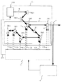
図1は、本実施例を適用した光学装置の一構成例である。図1中、1は所定の機能を奏する光学ユニット、2は素子のパラメータを制御信号(調整信号)CSの値に応じて変化させ得る調整可能な光学素子であり、3は調整を行わない光学素子である。光学素子2および光学素子3は、その光学ユニット1の構成要素である。4は、調整可能な光学素子2に接続する、調整可能な光学素子2のパラメータを制御信号CSの示す値に応じて変化させるための駆動機構である。5は、本発明の方法に従って、光学ユニット1を調整するための調整装置、6は、光学ユニット1(光学装置)の光出力の状態を観測するための観測装置である。この実施例では、調整装置5および観測装置6は光学ユニット1の外部装置となる。
【0039】
図1中、8、9はそれぞれ、光学装置に入力する光(入力光)、および光学装置から出力する光(出力光)である。
【0040】
図1中、7は調整光発生装置であり、光学ユニット1を調整するための調整光を発生させる。この調整光発生装置7は、調整を行わないときには停止して、入力光8には通常の入力光が入力される。この調整光は、調整装置5からの信号5Tに従って発生され、光学装置1の入力光8として光学装置1に入力される。調節光は光の強度の波長分布および空間分布が一定である連続光またはパルス光であり、光学装置1を調整するときの基準となるものである。この調整光は複数の種類の光を切り替えることも可能であり、この場合は、信号5Tに従って切替られるものである。
【0041】
調整光発生装置7は、調整装置5からの信号5Tに従って調整光を発生する装置のほか、調整装置5によらず独自に調整光を発生する装置とすることも可能である。さらには、調整光発生装置7を省略して、調整光の代わりに、光学装置に通常入力される入力光を調整光とみなすことも可能である。さらにまた、入力光の光源を光学装置に内蔵することも可能である。
【0042】
図1において、光学素子2および光学素子3の配置、およびかかる光学素子に関する光路は、その概念を示す例示であり、実際には光学装置の設計により決められる。同様に、駆動機構4に入力する制御信号CSの数は光学素子の調整に必要なパラメータの数に対応して決められる。
【0043】
調整可能な光学素子2および調整を行わない光学素子3は、ミラー、レンズ、光学フィルター、プリズム、回折格子、偏光素子、電気光学素子、音響光学素子、光学結晶(レーザー結晶)、スリット、および上記それらの光学素子の複合で構成される光学素子、等であり、光学ユニット1の構成要素として機能する。すなわち、光学装置において、調整可能な光学素子2および調整を行わない光学素子3は、光学ユニット1で取り扱う光の光路に設置され、その光を、別方向に反射、集光、光路の分割/合成、波長による選別、減衰、波長による光路の分別、偏光による光の選別、変調、波長変換等を行う。
【0044】
上記において、調整可能な光学素子2は本発明の方法で調整がなされる光学素子であり、調整を行わない光学素子3は、本発明の方法による調整が行われない光学素子であっても、ほかの方法、たとえば光学装置を組み立てた直後の粗調整など従来手法による調整を行うようにしても良い。
【0045】
光学素子2の素子パラメータ(パラメータ)とは、光学ユニット1内における光学素子2の位置、方向、光学特性であり、位置では、たとえば、直交座標系X軸、Y軸、Z軸のそれぞれの方向の変位量x、y、z、であり、方向では、たとえば、X軸を中心とした回転の量θx、Y軸を中心とした回転の量θy、Z軸を中心とした回転の量θzである。かかる光学特性とは、たとえば、反射率、透過率、吸収係数、増幅係数、波長変換効率、屈折率、偏光特性(リターデーション)、伝達特性(位相、光強度、横モード等)、分配比、変調率、および上記それらの波長特性、集光条件(焦点の形状、収差)、コヒーレンス、光路条件である。
【0046】
調整対象となる光学ユニット1は、上述のように調整される光学素子2と調整されない光学素子3から構成されており、この実施例では、調整される光学素子2のパラメータを製造後あるいは光学装置の移動等で振動や衝撃が与えられた後に微調整することにより、光学装置の特性が要求仕様を満たすようにする。しかしながらこの光学装置は、図2に例示したように、ある光学素子2のある一つのパラメータの調整が他のほとんどすべてのパラメータの調整結果に影響を及ぼすような光学装置であるので、多くの場合、調整探索空間が組み合わせ爆発を起こしてしまう。それゆえ、本発明に基づく遺伝的アルゴリズムを用いた後述する調整手法が非常に有効である。
【0047】
本実施例において、光学装置の機能が所定の仕様を満たすように光学素子2のパラメータが調整される。調整装置5の1構成例を図3に示す。図中、5Rはデータを保持するレジスタ、5RGは調整箇所の数のレジスタ5Rを備えたレジスタ群である。5Aは本発明の方法に従って調整手順を実行する調整アルゴリズム実行装置、5Fは光学装置の機能の評価値を計算する評価関数器である。図中、4は駆動機構で、4Cは比較回路,4Dは光学素子のパラメータを変更する駆動機構4を駆動するモータ駆動回路である(後で説明する。)。
【0048】
本実施例における調整では、上記駆動機構4は、図3に示す調整装置5内のレジスタ5Rに保持されているデジタル値に対応する制御信号CSに従って、調整される調整素子2のパラメータを変更する。該制御信号CSは、レジスタ5Rのデータに一対一に対応したアナログ信号あるいはデジタル信号である。ここにおけるレジスタ5Rは、光学素子2の調整箇所の総数と一致した個数だけ設けられる。レジスタ5Rは、保持したデジタル値を駆動機構に出力するとともに、調整装置5内の調整アルゴリズム実行装置5Aにより、保持している値を変更され得る。
【0049】
上記の調整アルゴリズム実行装置5Aは、遺伝的アルゴリズムに従って、複数のレジスタ5Rの保持値として最適な値を探索する。なお、調整装置5は、パーソナルコンピュータあるいはマイクロコンピュータ等の読み取り可能な記録媒体/記録媒体の読みだし装置を具備した電子計算機により構成することが可能であり、また、特開平9−294069号公報に公開されているプログラマブルLSI、あるいは、梶谷らによる論文「GAによるニューラルネットワークの構造学習回路の実現」(日本神経回路学会誌vol.5、No.4、pp.145〜153、1998年)に記載されている回路を用いて構成することもできる。
【0050】
上記の電子計算機に於いては、調整アルゴルゴリズム実行装置5Aおよび評価関数器5Fの機能を実現するプログラムがハードディスク、ROM(読みだし専用メモリ)、光ディスク、光磁気ディスク、フレキシブルディスク、磁気ディスク、フラッシュメモリ、強誘電体を利用したメモリ、磁性体を利用したMRAM、バックアップ機能をもつ半導体メモリ、等の記録媒体に格納されている。同様に、後述の駆動機構制御装置5Cの機能も電子計算機上で実現でき、このための調整方法に係るプログラム(調整を行うプログラム)が同様に上記の記録媒体に格納されている。
【0051】
また、上記の調整を行うプログラムは、ネットワークを経由して伝送・配信されるものであってもよい。
【0052】
観測装置6は、光学装置(光学ユニット1)の出力光を入力されて、その入力光を分析し、電気的な信号に変換した後、調整装置5に引き渡す。調整装置5は、評価関数器5Fによって調整光に対応する光学装置1の出力がどの程度理想的であるかの評価値を計算する。その評価値は、調整装置5内の調整アルゴリズム実行装置5Aに引き渡される。調整アルゴリズム実行装置5Aは、後述するように本発明の方法で最適な調整結果を探索する。
【0053】
本実施例では入力光および出力光の光路数がそれぞれ一ずつであるが、本発明では、光学装置1の入力光8および出力光9の光路数は、複数の場合を含む任意の場合で可能であり、また、例えば、励起光源を内蔵したレーザーのように入力光8を有しない場合でも可能である。また、双方向に光を取り扱う光学装置の場合でも可能である。なお、この場合には、信号の方向に応じて入力光8と出力光9が変わるので、調整光発生器7と観測装置6の接続を切り替えて本発明の調整を実施する。
【0054】
また、本発明の調整に用いられる出力光9は光学装置1の本来の出力光のみならず、光学装置の内部(光学ユニット1)から取り出しても良い。
【0055】
光学ユニット1における光学素子2の調整箇所の総数が複数であり、図2に例示するように、光学素子2の調整箇所において、ある調整箇所の調整が他のすべての調整箇所の調整結果に影響を及ぼすものであって、調整探索空間の組み合わせ爆発を起こす場合に、本発明は特に有効である。
【0056】
本実施例の光学ユニット1は、電気信号の調整信号に従って駆動機構4により調整される光学素子2、レジスタ群5RGを有する調整装置5により調整されることを大きな特徴としている。以下に本実施例の光学装置の動作説明を行う。
【0057】
光学素子2は、ミラー、レンズ、光学フィルター、プリズム、導波路型光学素子(光ファイバー、導波路型変調器、光ファイバーグレーティング)、半導体光部品(半導体ミラー、半導体吸収変調器)、回折格子、偏光素子、電気光学素子、音響光学素子、光学結晶(レーザー結晶)、スリット、および上記それらの光学素子の複合で構成される光学素子、等であり、調整装置5から出力される制御信号CSに対応して駆動機構4によりその位置、方向、光学特性のパラメータを変化させ得る光学素子である。
【0058】
そしてこの実施例は、かかる光学素子2の調整箇所の個数が複数であることを特徴としている。調整箇所が複数である場合はたとえ光学素子2の数が1であってもよい。光学素子2が複数の場合は、同一種類の光学素子であるか否かを問わない。また通常は、駆動機構4の数は光学素子2の調整箇所の同数である。ただし、駆動機構の一部、たとえば、モータに電流を流すための回路などは一体化してもよい。
【0059】
光学素子2は、駆動機構4によりそのパラメータを変化させるものである。可変するパラメータは上述のように、任意の座標系における位置、方向、光学特性であり、ある1つの調整箇所の変更、すなわち、ある1つの駆動機構4の動作により変化するパラメータの数は1とは限らない。以下に駆動装置4の構成例を示す。
【0060】
一方向の並進の移動が可能である光学素子2の駆動機構4の一構成例を図4に示す。図4中、401は該駆動機構の基台である。402は駆動され並進の動きをするステージであり、基台401上を一方向に動くことができるようにレールが設けられている(図示していない。)。該ステージ402には光学素子2が取り付けられている。403は雄ねじ、404は基台401に固定された雌ねじである。405は雄ねじ403を回転するためのモータ、406は雄ねじ403の回転した量(回転角)を検出するためのポテンショメータである。407はバネであり、雄ねじ403と雌ねじ404の間の隙間により位置の不確定さが生じることを防ぎ、また、雄ねじ403の移動量とステージ402の移動量が同じとなるように機能する。
【0061】
該駆動機構においては、モータ405により雄ねじ403が回転し、雌ねじ404が基台401に固定されていることから、雄ねじ403はその中心軸の方向に移動する。この移動量は雄ねじ403の回転角に比例した大きさである。雄ねじ403が一回転(回転角が360度)のとき、該移動量は雄ねじ403のねじ山のピッチに等しくなる。ステージ402は、雄ねじ402と同じ移動を行う。
【0062】
4Cは、制御信号CSと、ポテンショメータの示す回転角の信号(PS)を入力されて、制御信号CSに対応する回転角とポテンショメータの示す回転角を比較するための比較回路である。4Dは、比較回路4Cの出力に従ってモータ405を回転するための電流(MD)を出力するモータ駆動回路であり、比較回路の出力である制御信号CSに対応する回転角とポテンショメータの示す回転角が小さくなる方向にモータを回転する電流を出力する。
【0063】
以上の動作によって、該駆動機構は、該駆動機構に取り付けた光学素子2を、制御信号CSの示す値に対応する位置となるように並進移動させる。すなわち、該駆動機構は制御信号CSの示す値に対応して光学ユニット1内の光学素子2のパラメータを変化させる。
【0064】
図4の構成例の比較回路4Cおよびモータ駆動回路4Dを、調整装置5内に組み込むことも可能である。図5はこの一構成例を示している。図5中の5Cは、駆動機構制御装置で、ポテンショメータ406からの信号が入力されて図4の比較回路4Cおよびモータ駆動回路4Dと同じ機能を行う。ここで、図3と同じ参照符号のものは同じもの若しくは相当するものであることを表している。
【0065】
モータ405は直流モータのほか、圧電効果を利用するピエゾモータを使用してもよい。また、モータ405をステッピングモータとした場合、ステッピングモータに流す電流の状態に対応してモータの回転角度が制御できることから、ポテンショメータ406および比較回路4Cを省略する事が可能である。この場合、モータ駆動回路4Dは、制御信号CSが入力される。
【0066】
光学素子2において、二方向の並進を行うには、上記の図4の構成の駆動機構4を2段に重ねて使用すればよい。すなわち、2段に重ねた駆動機構のうち、下の段のステージ402と上の段の基台401を互いに固定するか、あるいは一体の構成とすればよい。このとき、下の段のステージ402と上の段の基台401の向きの関係は、平行であっても垂直であってもよい。さらには、任意の一定の角度であってもよい。
【0067】
光学素子2において、三方向の並進の移動を行うには、上述の二方向の並進の移動の場合と同様に、上記の図4の構成の駆動機構4を3段に重ねて使用すればよい。すなわち、3段に重ねた駆動機構4のうち、下の段のステージ402と中央の段の基台401を互いに固定するか、あるいは一体の構成とすればよく、中央の段のステージ402と上の段の基台401を互いに固定するか、あるいは一体の構成とすればよい。このとき、それぞれの段の基台401及びステージ402の向きの関係は、同様に平行であっても垂直であってもよく、任意の一定の角度であってもよい。
【0068】
光学素子2に対して一軸の回転を行う駆動機構4の一構成例を図6に示す。図6中、401は該駆動機構の基台である。402は駆動され並進の動きをするステージであり、410で示す支点を中心に回転する。該ステージ402に光学素子2が取り付けられる。403は雄ねじ、404は基台401に固定された雌ねじである。405は雄ねじ403を回転するためのモータ、406は雄ねじ403の回転した量(回転角)を検出するためのポテンショメータである。407はバネであり、雄ねじ403と雌ねじ404の間の隙間により位置の不確定さが生じることを防ぎ、また、雄ねじ403の移動量と一対一対応したステージ402の回転量が得られるように機能する。
【0069】
該駆動機構においては、モータ405により雄ねじ403が回転し、雌ねじ404が基台401に固定されていることから、雄ねじ403はその中心軸の方向に移動する。この移動量は雄ねじ403の回転角に比例した大きさである。雄ねじ403が一回転(回転角が360度)のとき、該移動量は雄ねじ403のねじ山のピッチに等しくなる。4Cは、制御信号CSに対応する回転角とポテンショメータの示す回転角を比較するための比較回路である。
【0070】
4Dは、比較回路4Cの出力に従ってモータ405を回転するための電流を出力するモータ駆動回路であり、比較回路の出力である制御信号CSに対応する回転角とポテンショメータの示す回転角が小さくなる方向にモータを回転する電流を出力する。雄ねじ403の移動によりステージ402が支点410を中心とする回転を行う。以上の動作によって、該駆動機構は、該駆動機構に取り付けた光学素子2を、制御信号CSの示す値に対応する方向となるように回転させる。すなわち、該駆動機構は制御信号CSの示す値に対応して該光学装置2のパラメータを変化させる。
【0071】
モータ405は直流モータのほか、圧電効果を利用するピエゾモータを使用してもよい。また、モータ405をステッピングモータとした場合、ステッピングモータに流す電流の状態に対応してモータの回転角度が制御できることから、ポテンショメータ406および比較回路4Cを省略することが可能である。この場合、モータ駆動回路4Dには、制御信号CSが入力される。
【0072】
光学素子2において、二軸の回転を行うには、上記の図6の構成の駆動機構を2組使用すればよい。さらには、支点410、バネ407を共通にして、図7に示す構成とすることも可能である。図7において、403a、403bは2つの軸に対応した回転を得るための雄ねじであり、410は共通の支点、407は共通のバネである。図7において、雄ねじ403a、403bの移動に必要なほかの構成要素の記載を省略してある。雄ねじ403a、403bがそれぞれ独立して制御信号CSに対応した位置に移動を行い、2軸の独立した回転が得られる。
【0073】
光学素子2において、三軸の回転を行うには、上述の二軸の回転の場合と同様に、上記の図6の構成の駆動機構を3組使用すればよい。
【0074】
1つの光学素子2の変化し得るパラメータが並進の移動と回転の複合である場合には、上述の並進の移動の場合の構成例と、回転の場合の構成例を組み合わせることで構成できる。
【0075】
光学素子2が可変形ミラーである場合、取り扱う光の波面の制御が可能である。可変形ミラーの光学素子2およびその駆動機構4の一構成例を図8および図9に示す。図8は、この可変形ミラーの構成例の断面を示す図であり、図9は、この可変形ミラーの構成例の電極配置を示す平面図である。
【0076】
図8において、201は制御信号CSの示す値に対応して変形するミラー、202はミラーの支持構造、203は複数個の電極である。4AMは制御信号CSの値に応じて電圧を出力する増幅器である。本構成例では、1つの可変形ミラーなる光学素子2と複数の駆動機構4が一体の構成となっている。
【0077】
該変形するミラー201は、導電性の物質でできており、便宜上接地電位であるとする。複数の電極203は、該ミラー201に対向し、かつ、近接して等距離に設置されている。このとき、電極203に電圧を印加すると、静電引力により電極203に近接した部分のミラー201が引き寄せられる。その結果、該ミラー201は変形する。ここで、電極203および増幅器4AMは駆動機構4として機能する。
【0078】
電極203が複数あることから、それぞれの電極に印加される電圧に応じてそれぞれの電極近傍のミラーが引き寄せられることになる。このとき、ミラー201の変形の自由度は電極203の数と同じである。電極203は、図9に示す如く配置される。上記の構成例では、一つの可変形ミラーの電極の数、ミラー201の変形の自由度、調整箇所の数はともに37である。
【0079】
すなわち、該ミラー201は、入力される制御信号CSと同数のパラメータを有し、それと同数の自由度で変形する。ここで、ある電極203に対応する場所のミラー201の変形量は、該電極203に隣接する電極203の電圧により大きく影響される。そのため、複数の調整されるパラメータは、図2に示す如く該パラメータの調整結果に相互に影響を及ぼす。
【0080】
可変形ミラーの別の構成例について、図10にその断面を示す。図10中、4PZはピエゾ素子、204は絶縁体の支持構造である。このほか図8の場合と同様のものに同じ符号を付している。電極203の配置は図9に示す構成例と同様である。
【0081】
すなわち、入力される制御信号CSは増幅器4AMで増幅され、該制御信号CSに対応した電圧がピエゾ素子に印加される。これにより、ピエゾ素子が機械的に変形し、ミラー201が変形する。従って、上記の構成例と同様に、ミラーの形状を制御信号CSの示す値に応じて可変できる。この構成例では、ミラー201がピエゾ素子4PZ、電極203、および支持構造204により機械的に固定されているので、外部からの振動による影響を低減したい場合に有効である。
【0082】
さらにまた、可変形ミラーの別の構成例として、図10におけるピエゾ素子4PZを、ピエゾ素子と機械的に変位を生ずる駆動機構の複合としても良い。該駆動機構には、たとえば図4で示した駆動機構を用いることができる。この場合、ミラーの形状の大きな変位を該駆動機構で生じせしめ、変位の微調整をピエゾ素子により行うことで、大きな変位を高い精度で得ることができる。
【0083】
可変する素子パラメータが透過率、あるいは、吸収係数である場合の光学素子の一構成例を、図11に示す。図11中、210は半導体接合素子、211は入力光、212は出力光、213は電極、4AMは増幅器であり、本発明における駆動機構4に対応する。制御信号CSが増幅器4AMに入力され、その制御信号CSに対応した電圧が、電極213より、半導体接合素子210の逆バイアス電圧として該半導体接合素子に印加される。このとき、半導体接合素子210内部の物性値が変化し、光の透過率、あるいは、吸収係数が変化する。
【0084】
可変する素子パラメータが反射率である場合は、図11の構成で半導体接合素子210の光路と垂直の面の一つに反射膜を形成した構成が可能である。この場合、入射光と反射光の光路は同一となり、制御信号CSの示す値によって反射率が変化する。
【0085】
可変する素子パラメータが複屈折率である場合の光学素子の一構成例を、図12に示す。図12中、220は液晶、221は偏光子、222は位相調整器である。このほか、図11と同様の構成要素に同じ符号を付している。液晶220は電圧の印加により複屈折率が変化する。液晶220は、液晶の代わりに複屈折を有する電気光学結晶としても良い。位相調整器222は、たとえば1/2波長板もしくは1/4波長板である。この構成例も上記の透過率を可変する場合と同様にして、制御信号CSに対応した電圧が、液晶220に印加され、液晶の複屈折率が変化し、該光学素子を伝達する光の偏光特性(リターデーション)が変化する。
【0086】
可変する素子パラメータが伝達特性(位相/光強度)である場合の光学素子の一構成例を、図13に示す。図13中、230は電気光学結晶、231は分波器、232は合波器、233はミラー、221は偏光子である。このほか、図11と同様の構成要素に同じ符号を付している。電気光学結晶230は液晶などでもよい。分波器および合波器はたとえば偏光ビームスプリッタである。入力光211は分波器231で2分され、一方の光は電気光学結晶230により制御電圧の示す値に応じて位相が変化する。この光と分波器231からの光が合波器232で合成される。このとき、制御信号CSに対応して該光学素子の出力光の光強度が変化する。
【0087】
可変する素子パラメータが分配比である場合の光学素子の一構成例を、図14に示す。図14中、230は偏光を制御する電気光学結晶、231は分波器であり、たとえば、偏光ビームスプリッタである。221は偏光子である。212a、212bは二つに分配される出力光である。このほか、図11と同様のものには同じ参照符号を付している。上記の光学素子と同様に、入力光211は、電気光学結晶230により制御電圧の示す値に応じて偏光の状態が変化する。この光は分波器231で偏光の状態に応じて分配される。その結果、制御信号CSに対応して該光学素子の分配比が変化する。
【0088】
可変する素子パラメータが変調率である場合の光学素子の一構成例を、図15に示す。図15中、4VAは電気信号の利得可変増幅器、230は電気光学結晶である。このほか、図11と同様の構成要素に同じ符号を付している。入力光211は、電気光学結晶230において変調信号により変調される。このとき、利得可変増幅器4VAの利得を制御信号CSで可変することにより、制御信号CSに対応して該光学素子の変調率が変化する。
【0089】
可変する素子パラメータが振幅・位相特性の波長依存性(波長特性)である場合の光学素子の一構成例を、図16に示す。図16中、250は複数の制御信号CSによりその透過特性が制御される液晶パネル、251は回折素子、252はレンズである。回折素子251はたとえば回折格子もしくはプリズムである。入力光211は、回折素子251およびレンズ252によって波長別に光路が振り分けられる。そして、液晶パネル250は複数の制御信号CSの示す値に応じて複数の光路の振幅・位相特性が変化する。その結果波長ごとに光の振幅・位相が変化する。そしてレンズ252および回折素子251により波長別であった光路が一つの光路に合成される。その結果、複数の制御信号CSに対応して該光学素子の振幅・位相特性の波長依存性が変化する。
【0090】
上記の光学特性を可変する光学素子は、その光学特性をもっぱら電気的に可変するものであるが、光学素子2がその光学特性を光学的に可変する場合も可能である。
【0091】
光学素子2が該光学素子の光学特性を光学的に可変するものには、波長変換結晶、光増幅媒体、光変調器、光スイッチング素子がある。波長変換結晶は、光学結晶であり、分極振動の非線形性に基づく非線形光学現象を利用したものである。光増幅媒体には、レーザー結晶、有機色素、半導体、光増幅導波路がある。
【0092】
レーザ結晶は、レーザー準位(レーザー遷移を起こすことが可能なエネルギー準位)の反転分布を形成し、誘導放出を利用して光を増幅する。有機色素は有機色素中にレーザー準位の反転分布を形成し、誘導放出を利用して光を増幅する。光増幅導波路は、エルビウムなどのレーザ準位を有する元素を導波路に添加したものであり、たとえば、エルビウム添加光ファイバーである。
【0093】
光学素子2が該光学素子の光学特性を音響的に可変するものは、音響光学素子であり、たとえば、光学素子の光路に設置される媒質に超音波を印加して、この超音波の定在波による媒質の物性値の変化により光学素子の光学特性を変化させるものである。
【0094】
さらにまた、光学素子2が上記の光学素子2の複合であるものであってもよい。
【0095】
次に、上記光学装置の調整のための、本発明の調整方法の第1実施例について説明する。
【0096】
上記光学装置が製造された後、調整工程で、図1に示すように、光学ユニット1、調整装置5、観測装置6および調整光発生装置7がその光学装置にそれぞれ配置される。調整光発生装置7は、光学装置に調整光8aを入力し、調整装置5は、図17に示す処理手順に従って、レジスタ群5RGのレジスタ値の設定を行う。
【0097】
この処理手順では、まずステップS1で、人手により粗調整を行い光学装置を動作させ、そのときの各光学素子の素子パラメータ値を計測しその値を初期設定値としてレジスタ5Rに書き込んでレジスタ値として保持させ、次のステップS2で、調整光発生装置7が調整光を出力して、その調整光に対し光学装置を動作させ、次のステップS3で、その光学装置の光出力を観測装置6が観測してその結果を調整装置5に送り、次のステップS4で、調整装置5が、送られてきた観測値を使用して、光学装置の性能が、所定の仕様を満たす許容範囲にあるか否かを判定する。
【0098】
ここで許容範囲に無い場合には、ステップS5で、調整装置5が、レジスタ群5RGが保持しているレジスタ値を変更し、次のステップS6で、駆動機構4が停止するまで一定時間待機し、次のステップS7で、終了条件(具体的には後述する。)をみたしたか否かを判断し、終了条件をみたしていればステップS8で不良品処理を行った後に当該処理を終了するが、終了条件をみたしていなければステップS2へ戻る、という一連の処理が繰り返し実行される。そして上記ステップS4で、光学装置の性能が所定の仕様を満たすものとなったとの判定が得られた場合には、当該処理を終了する。
【0099】
上述した初期設定値からレジスタ値を変更する方法については、いくつかの方法を使用することができ、以下にその例を示す。すなわち、第1の方法は、想定されるレジスタ値の範囲におけるすべての組み合わせについて、適当な順序で順次設定値を切り替えていく方法であり、第2の方法は、乱数的に設定値を発生させる方法である。そして第3の方法は、人手による粗調整結果を初期設定値とし、その初期設定値から+方向と−方向に設定値を変化させる方法である。
【0100】
調整対象の光学ユニット1内に調整される光学素子2の数が少なく、レジスタ値の組み合わせ爆発を生じない場合は、第1、第2の方法を用いることができる。しかし、本実施例は、調整される光学素子2の数が多く、調整される素子パラメータの調整探索空間において組み合わせ爆発の発生が想定される場合であるので、第3の方法を使用する。このとき、遺伝的アルゴリズムと呼ばれる方法を使用する。以下では、遺伝的アルゴリズムを用いた光学装置の調整方法について説明する。
【0101】
上記遺伝的アルゴリズムの参考文献としては、例えば、出版社ADDISON-WESLEY PUBLISHING COMPANY, INC. が1989年に出版した、David E. Goldberg 著の「Genetic Algorithms in Search, Optimization, and Machine Learing 」がある。なお、本発明でいう遺伝的アルゴリズムとは、進化的計算手法のことをいい、進化的戦術(Evolution Strategy: ES)の手法も含むものである。進化的戦術の参考文献としては、例えば、出版社John Wiley & Sons が1995年に出版した、H. P. Schwefel 著の「Evolution and Optimum Seeking」がある。
【0102】
光学装置の性能は、複数の素子パラメータ値を引数とする評価関数Fで表すことができる。光学装置の性能が所定の仕様を満たすようにすることは、評価関数Fを最適にするパラメータ値を求めることと等価である。本発明者はこの点に着目し、光学装置の調整に上記の遺伝的アルゴリズムを適用可能なことを発見した。調整装置5は、この遺伝的アルゴリズムにしたがってレジスタ群5RGのレジスタ値を変更する。
【0103】
遺伝的アルゴリズムでは、まず遺伝子を持つ仮想的な生物の集団を設定し、あらかじめ定めた環境に適応している個体が、その適応度の高さに応じて生存し、子孫を残す確率が増えるようにする。そして、遺伝的操作と呼ばれる手順で親の遺伝子を子に継承させる。このような世代交代を実行し、遺伝子および生物集団を進化させることにより、高い適応度を持つ個体が生物集団の大勢を占めるようになる。そしてその際の遺伝的操作としては、実際の生物の生殖においても生じる、遺伝子の交叉、および突然変異等が用いられる。
【0104】
図18は、かかる遺伝的アルゴリズムの概略手順を示すフローチャートであり、ここでは、初めにステップS11で、個体の染色体を決定する。すなわち、世代交代の際に親の個体から子孫の個体に、どのような内容のデータをどのような形式で伝えるかを定める。図19に染色体を例示する。ここでは、対象とする最適化問題の変数ベクトルxを、M個の記号Ai(i=1、2、・・M)の列で表わすことにし、これをM個の遺伝子座からなる染色体とみなす。各記号Aiは遺伝子であり、これらのとりうる値が対立遺伝子である。図19中、Chは染色体、Gsは遺伝子座を示し、遺伝子座の個数Mは5である。対立遺伝子としては、ある整数の組、ある範囲の実数値、単なる記号の列などを問題に応じて定める。図19の例では、a〜eのアルファベットが対立遺伝子である。このようにして記号化された遺伝子の集合が個体の染色体である。
【0105】
上記ステップS11では次に、各個体が環境にどの程度適応しているかを表わす適応度の計算方法を決定する。その際、対象とする最適化問題の評価関数の値がより高い変数あるいはより低い変数ほど、それに対応する個体の適応度が高くなるように設計する。またその後に行う世代交代では、適応度の高い個体ほど、生き残る確率あるいは子孫を作る確率が他の適応度の低い個体よりも高くなるようにする。逆に、適応度の低い個体は、環境にうまく適応していない個体とみなして、消滅させる。これは、進化論における自然淘汰の原理を反映したものである。すなわち適応度は、生存の可能性という面から見て各個体がどの程度優れているかを表わす尺度となる。
【0106】
遺伝的アルゴリズムでは、探索開始時においては、対象とする問題は一般にまったくのブラックボックスであり、どのような個体が望ましいかはまったく不明である。このため通常、初期の生物集団は乱数を用いてランダムに発生させる。従ってここにおける手順でも、ステップS12で処理を開始した後のステップS13では、初期の生物集団は乱数を用いてランダムに発生させる。なお、探索空間に対して何らかの予備知識がある場合は、評価値が高いと思われる部分を中心にして生物集団を発生させるなどの処理を行うこともある。ここで、発生させる個体の総数を、集団の個体数という。
【0107】
次にステップS14で、生物集団中の各個体の適応度を、先にステップS11で決めた計算方法に基づいて計算する。各個体について適応度が求まったら、次にステップS15で、次の世代の個体の基となる個体を集団から選択淘汰する。しかしながら選択淘汰を行うだけでは、現時点で最も高い適応度を持つ個体が生物集団中に占める割合が高くなるだけで、新しい探索点が生じないことになる。このため、次に述べる交叉と突然変異と呼ばれる操作を行う。
【0108】
すなわち、次のステップS16では、選択淘汰によって生成された次世代の個体の中から、所定の発生頻度で二つの個体のペアをランダムに選択し、染色体を組み変えて子の染色体を作る(交叉)。ここで、交叉が発生する確率を、交叉率と呼ぶ。交叉によって生成された子孫の個体は、親にあたる個体のそれぞれから形質を継承した個体である。この交叉の処理によって、個体の染色体の多様性が高まり進化が生じる。
【0109】
交叉処理後は、次のステップS17で、個体の遺伝子を一定の確率で変化させる(突然変異)。ここで、突然変異が発生する確率を突然変異率と呼ぶ。遺伝子の内容が低い確率で書き換えられるという現象は、実際の生物の遺伝子においても見られる現象である。ただし、突然変異率を大きくしすぎると、交叉による親の形質の遺伝の特徴が失われ、探索空間中をランダムに探索することと同様になるので注意を必要とする。
【0110】
以上の処理によって次世代の集団が決定され、ここでは次に、ステップS18で、生成された次世代の生物集団が探索を終了するための評価基準を満たしているか否かを調べる。この評価基準は、問題に依存するが、代表的なものとして次のようなものがある。
・生物集団中の最大の適応度が、あるしきい値より大きくなった。
・生物集団全体の平均の適応度が、あるしきい値より大きくなった。
・生物集団の適応度の増加率が、あるしきい値以下の世代が一定の期間以上続いた。
・世代交代の回数が、あらかじめ定めた回数に到達した。
【0111】
上述の如き終了条件(評価基準)の何れかが満たされた場合は、ステップS19へ進んで探索を終了し、その時点での生物集団中で最も適応度の高い個体を、求める最適化問題の解とする。終了条件が満たされない場合は、ステップS14の各個体の適応度の計算の処理に戻って探索を続ける。このような世代交代の繰り返しによって、集団の個体数を一定に保ちつつ、個体の適応度を高めることが出来る。以上が遺伝的アルゴリズムの概略である。
【0112】
上で述べた遺伝的アルゴリズムの枠組みは、実際のプログラミングの詳細を規定しない緩やかなものとなっており、個々の問題に対する詳細なアルゴリズムを規定するものではない。このため、遺伝的アルゴリズムを本実施例の光学装置の調整に用いるには、以下の項目を光学装置の調整用に実現する必要がある。
(a) 染色体の表現方法
(b) 個体の評価関数
(c) 選択淘汰方法
(d) 交叉方法
(e) 突然変異方法
(f) 探索終了条件
【0113】
図20は、本実施例における遺伝的アルゴリズムを用いた調整装置5の処理手順を示すフローチャートである。なお、この図20の処理は、図17のステップS3〜ステップS5の処理を具体的に示すものである。本実施例は、遺伝的アルゴリズムの染色体として、レジスタ5のレジスタ値を直接用いることを大きな特徴としており、これにより、染色体の情報をレジスタ値に変換するための処理等を不要とすることができる。
【0114】
このことを図21を例に具体的に説明する。この図は、図4および図6に示した駆動装置を調整する場合の例であり、レジスタ5Rは、+4.32、−15.67、+3.47、−9.71等の値を保持している。これらの値を直列に接続したものが染色体であり、この例の場合、染色体中の各遺伝子が+4.32、−15.67、+3.47、−9.71等の値をとることになる。レジスタ5Rの値は駆動機構4内のポテンショメータ406の値に対応しているので、ポテンショメータ406の値がレジスタ5Rで指示された値になるように光学素子2が制御される。ポテンショメータ406の値と素子パラメータの値は一対一に対応するので、遺伝的アルゴリズムの遺伝子の値と素子パラメータの値は一対一に対応することになる。
【0115】
図20の処理で使用する、遺伝的アルゴリズムの個体の評価関数Fとしては、個体の染色体が表現するレジスタ値で光学ユニットを設定したのち動作させ、観測装置6によって観測された光出力が理想的な出力にどのくらい近いかを表す関数を用いる。
【0116】
図20に示す処理で用いるために、先に図17のステップS1で遺伝的アルゴリズムの初期集団として、一様乱数を用いて個体を複数作成する。つまりこの場合には、初期集団の各染色体の各遺伝子の値は上限値と下限値のあいだのランダムな実数値をとることを意味する。但し、素子パラメータの誤差の傾向について何らかの予備知識が存在する場合には、より適応度が高いと思われる個体を初期集団として作成することができる。
【0117】
観測装置6から送られてきた観測結果から、評価関数器5Fにより上記評価関数を用いて適応度を計算する。その後調整アルゴリズム実行装置5Aにより、光学装置1の性能が所定の仕様を満たす許容範囲にあるか否かをステップS23で判定し、許容範囲に無い場合には、ステップS24の選択淘汰、ステップS25の交叉、ステップS26の突然変異およびステップ27、ステップS28の局所学習の処理(後述する。)を行って、次世代の個体の集団(解の候補の集団)を作り出す。
【0118】
しかして、ステップS23での判断で光学装置の性能が所定の仕様を満たしたときに、調整処理は終了するが、一定世代数繰り返して調整処理をおこなっても仕様を満たす染色体(レジスタ値)が得られない場合には、調整対象の光学装置は不良品と判断され、図17のステップS8で不良品としての処理を行う。なお、所定の仕様にたとえば出力光強度等の評価値をできるだけ増大もしくは減少せよ、という指示がある場合には、ステップS23で調整処理を終了する条件としては、世代数が一定数をこえたか否かという条件を用い、不良品処理は行わない。
【0119】
上記ステップS24の選択淘汰処理においては、図22のフローチャートに示す方法を用いる。この方法は、まずステップS31およびステップS32で、集団中からランダムにふたつの個体A、Bを選び、次いでステップS33〜ステップS35で、そのふたつの個体A、Bのうち、より適応度の値が大きいほうの個体を次世代に生き残らせる個体とする。そして生き残った個体の数が集団の個体数に達するまで、ステップS36からステップS31へ戻ってその操作をくり返す。この方法では、適応度の大きい個体が次の世代の個体として選ばれる可能性が高いが、個体A、Bをランダムに選択しているため適応度が低い個体でも次世代の個体として選ばれる可能性が残されることになる。このようにするのは、適応度が高い個体だけ残すと、集団の収束性が高まり、局所的な最適解にとらわれて調整に失敗しやすくなるためである。
【0120】
上記ステップS25の交叉処理では、図23の説明図に示す方法を用いる。これは染色体をランダムな位置で部分的に入れ替える操作であり、1点交叉と呼ばれる手法である。図23では、Ch1およびCh2が選択淘汰の結果生き残った親A、Bの染色体であり、ここにおける交叉処理では、これらの染色体を、ランダムに選んだ交叉位置CPで切断する。図23の例では、左から2番目の遺伝子と3番目の遺伝子の間を交叉位置としている。そして、切断した部分的な遺伝子型を入れ替えることによって、染色体Ch3およびCh4をそれぞれ持つ子A' 、子B' を生成し、これらをもとの個体A、Bと置き換える。
【0121】
ステップS25での交叉にひき続いて実行する上記ステップS26の突然変異は、各染色体の遺伝子にガウス分布N(0、σ)に従って発生させた正規乱数を加算する操作とした。図24に突然変異の例を示す。この図では、染色体Ch5に対して、ガウス分布に従って発生させた正規乱数Nが加算されて染色体Ch6に変更されている。
【0122】
ステップS26での突然変異が終了したのち、得られた染色体の値をレジスタ群5RGに書き込む。その後、駆動機構制御装置5Cが、素子パラメータの値がレジスタ値に対応した値になるように駆動機構4を制御する。駆動機構制御装置5Cがない場合は、駆動装置内にある比較器4Cおよびモータ駆動回路4Dが素子パラメータがレジスタ値に対応した値になるように制御を行う。この制御には、観測装置6が出力光の状態を観測するのに要する時間と比較して、一般的に10から100倍の時間を要する。
【0123】
そこで、この制御を行っている最中にも観測装置6を動作させ、その観測値をもちいて効率的に探索を行う調整方法を発明した。その方法を局所学習と呼ぶことにし、ステップS27、ステップS28で実行する。局所学習を行う場合は、図5に示した調整装置5を用いる。なお、観測装置6が出力光の状態を観測するのに要する時間が、素子パラメータを制御するのに必要な時間と比較して大きい場合は、この局所学習はおこなわずにステップS27のみを行う。
【0124】
上記ステップS28の局所学習処理は、図25の説明図に示す方法を用いる。この方法は、まず図20のステップS27に対応する図25のステップS41でレジスタ値を変更し、図5の駆動機構制御装置5Cを動作させ、ステップS42で観測装置6により光学装置の出力光を観測し、それと同時に駆動機構制御装置5Cが素子パラメータの値をステップS43で計測する。ステップS44では、駆動機構制御装置5Cおよび評価関数器5FがステップS42とステップS43で得られた出力光の観測値と素子パラメータの値を調整アルゴリズム実行装置5Aに送り、調整アルゴリズム実行装置5Aがそれらを組としてメモリ5Mに保存する。
【0125】
そしてステップS45において、駆動機構制御装置5Cで素子パラメータの値がレジスタ値に対応した値になったと判定されるまで、上記ステップS42〜ステップS44を繰り返す。ステップS46では、素子パラメータの値がレジスタ値に対応した値になったと判定されたのち、調整アルゴリズム実行装置5Aにおいて、メモリ5Mに保存された出力光の観測値と素子パラメータの値の組のうち、もっとも評価関数Fの値が大きくなる組、すなわち局所的な最適解、を選び出す。最後にステップS47において、ステップS46で選び出された組の素子パラメータ値を用いて、それに対応するレジスタ値を求めその値で染色体を書き換える。
【0126】
上記局所学習処理において、調整対象の素子パラメータが2個の場合の動作例を、図26を用いて説明する。まず、上記ステップS41でレジスタ値を変更する前の素子パラメータの値が(XS,YS)であったとする。そして、ステップS41で変更したレジスタ値に対応する素子パラメータの値が(XE,YE)であるとする。このとき、ステップS42からステップS45のループにおいて、素子パラメータの値は、(XS,YS)から(XE,YE)へと駆動機構制御装置5Cによって徐々に変化させられる。そのときに、ステップS44により、変更途中の素子パラメータの値と、その値に対応する観測結果の組が複数個メモリに保存される。
【0127】
次に、ステップS46において、メモリに保存された上記素子パラメータ値と観測値の組のうち、観測結果より算出される評価関数Fの値(適応度)がもっとも大きくなる組を選び出す。この例の場合は、素子パラメータが(XM,YM)のときに評価関数値が最大のFMをとるので、ステップS46で(XM,YM)の組が選ばれる。最後にステップS47で、染色体の値が、素子パラメータ(XM,YM)に対応する値に書きかえられる。
【0128】
図26の例の場合、局所学習を行わない場合は、素子パラメータが(XS,YS)のときと(XE,YE)のときの二通りしか探索(観測)を行わないので、評価関数値をFMにする素子パラメータ(XM,YM)を発見することはできない。しかしながら、局所学習を行う場合は、素子パラメータ変更中にも観測をおこなうので、(XS,YS)(XM,YM)以外の複数個の素子パラメータ値(おおむね10から100個程度)において探索を行っているので、(XM,YM)を発見することができる。さらに、この(XM,YM)に対応したレジスタ値で染色体が書き換えられるので、探索効率が大幅に改善される。
【0129】
上述したように、本実施例の光学装置では、複数の光学素子に、素子パラメータを変更可能な素子2を使用し、それらの光学素子2の素子パラメータを光学装置の性能が好適となるように探索する。従って、熟練者による手動の調整および精度の高い光学素子を必要とすることなく、また、精度の高い駆動装置を必要することなく、光学装置を所定の仕様を満たすように自動的に調整することができる。このことは、従来技術による場合より少ない労力で、従来技術による場合より高性能が得られることを意味する。
【0130】
次に、本発明の第1実施例の光学装置の一変形例について説明する。先の実施例では、調整される光学素子2が光学装置内に実装される一方、調整装置5および観測装置6は外部装置として光学ユニット1に脱着可能に接続される。しかしながら本発明では、調整装置5や観測装置6に相当する機能を調整手段として光学ユニット1に組み込んだ装置にしてもよい。
【0131】
このように構成された変形例を図27に示す。ここでは光学装置1A内に光学ユニット1、調整装置5および観測装置6に相当する機能が組み込まれている。
【0132】
すなわち、図27の光学装置の例は、光学装置1Aの入力光8および出力光9の光路部分に、ミラーを利用した切換スイッチ13が設置されている。この切換スイッチ13は、図示例のように光学装置1A内に設けられていても良いが、光学装置1A外に設けても良い。ここで、切換スイッチ13を操作すると、光学ユニット1の出力光が観測装置6に入力されるとともに、調整装置5、調整光発生装置7が動作を開始し、設定値の調整を行う。設定が終了したら、切換スイッチ13の操作で、光学ユニット1の出力光を本来の出力光路側に切り替える。なお、この例では、仕様を満たす解(レジスタ値)が得られない場合に警告表示をする表示器14が設けられている。
【0133】
かかる変形例によれば、組立後の光学装置1Aの調整だけでなく、ユーザが光学装置1Aを組み込んだ製品を購入した後、ユーザ自身が光学装置1Aの調整を随時行うこともできる。これにより、光学装置1Aを移動運搬した場合や、光学装置1Aが置かれた環境の温度その他が変化した場合等に、光学装置の性能特性に変化が生じても、その変化を補償することができ、ひいては、光学素子の素子パラメータのずれによる光学装置の機能・性能の低下を改善することができるというメリットがある。なお、切換スイッチ13は手動に限らず、光学装置1Aの起動時に自動切換するように構成することもできる。
【0134】
また、この変形例は、調整装置5として先の梶谷らによる論文記載の遺伝的アルゴリズム実行回路等を用いることにより、小型化にも適している。
【0135】
さらにまた、この変形例によると、ユーザーが随時調整可能であるから、光学素子のホルダーや光学ユニット1の基台(光学定盤)の剛性が従来のものより低い物であってもよい。その結果、光学ユニット1の大幅な軽量化、小型化、ひいてはコストの低減というさらなる効果が得られる。
【0136】
次に、本発明の光学装置の第2実施例としての超短パルスレーザー装置(発生する光パルスの幅がフェムト秒領域から10ピコ秒であるレーザー装置)の一構成例を示す。図28は、本発明の光学装置の第2実施例としての超短パルスレーザー装置を例示する構成図である。
【0137】
超短パルスレーザー装置は、発生する光パルスのパルス幅がフェムト秒領域と非常に短く、かつ、光パルスの強度の尖頭値(ピーク値)が非常に大きいという特徴があり、それゆえ、超高速サンプリング測定技術に代表される計測技術のみならず、光通信技術、医療技術、加工技術においても超短パルスレーザー装置は高い有用性がある。
【0138】
超短パルスレーザー装置は、励起光源、光学結晶、共振器(キャビティー)を構成する複数のミラーおよびプリズムなどの光学素子を該レーザー装置の主要な構成要素としている。そして、超短パルスレーザの機能には、発生する光パルスの強度ができるだけ高く、パルス幅ができるだけ短く、光パルスの強度のピーク値ができるだけ大きく、さらにまた、必要な励起光の強度がなるべく小さいという特性が望まれる。
【0139】
実際に製造される超短パルスレーザー装置では、製造工程における加工・組立精度の限界、移動・運搬時の振動や衝撃、設計上の誤差等に起因する該光学素子の位置や方向(パラメータ)の誤差のために、光学素子の作用が完全ではなくなり、その結果、光パルスの強度が低下し、パルス幅が長くなり、光パルスの強度のピーク値が低下し、必要な励起光の強度が高くなるといった機能の低下が起きてしまう。
【0140】
そこで、この第2実施例では、超短パルスレーザー装置を構成する光学素子のうちの複数の光学素子のパラメータを可変にし、該レーザの機能が高くなるように遺伝的アルゴリズムを用いて調整を行う。図28は、この第2実施例の超短パルスレーザー装置の構成を示しており、この超短パルスレーザー装置(以下、「レーザー装置」と称する)1Lは、第1実施例における光学ユニット1に該当する。なお、図1に使用されたと同様のものにはそれと同一の参照符号を付している。
【0141】
図28は、本発明の光学ユニットを適用した超短パルスレーザー装置の一構成例であり、この実施例においては、調整装置5および観測装置6は外部装置となる。レーザー装置1Lにおいて2M1から2M4は、制御信号CSが示す値に応じてパラメータを変化させる光学素子としての、パラメータを変化させ得るミラー、2P1および2P2は、これも制御信号CSが示す値に応じてパラメータを変化させる光学素子としての、パラメータを変化させ得るプリズムである。3M1および3M2は、本発明による方法での調整を行わない光学素子としてのミラー、3Cはこれも本発明による方法での調整を行わない光学素子としての光学結晶(レーザー結晶)である。
【0142】
7PBはレーザー装置の励起光を発生する光源(励起光源)であり、励起光源7PBは実施例1(図1)における調整光発生装置に対応しており、調整対象の光学装置すなわちレーザ装置1Lに内蔵された構成である。そして、光学結晶3C、およびミラー2M1から2M4の部分は、光が2M1と2M4の間を往復するため共振器(キャビティー)を構成する。この共振器を2Rとする。この共振器2Rが後述するように本発明の方法により調整される。
【0143】
また図28中、4は駆動機構であり、この駆動機構4は、保持回路としてのレジスタ5Rに保持されているデジタル値に対応する電気的信号を、制御信号CSとして、光学素子である2M1から2M4、および2P1、2P2、に供給する。ここで、駆動機構4およびレジスタ5Rは、調整箇所の数(図28の構成では14)だけ設けられる。
【0144】
上記駆動機構4は実施例1で用いた図4から図7に示す構成が利用できる。それぞれの調整箇所のパラメータは、レジスタ5Rの32ビットのデータに応じてポテンショメータ406の示す値が該データに対応した値となるようにモータ405が回転し、光学素子2の位置あるいは方向が変化する。
【0145】
図28中、8は励起光源により発生した励起光であり、9はレーザー装置1Lの出力光である。6はレーザー装置1Lの出力光9を観測して、光強度、パルス強度、あるいはパルス強度に関連した量(たとえば、レーザーパルス光により化合物半導体中に2光子吸収により誘起される電流値)、等、あるいはそれらの組み合わせを演算した結果を出力するものである。
【0146】
そして5は調整装置であり、遺伝的アルゴリズムに従って、第1実施例に詳述したと同様の方法で、複数のレジスタ5Rの保持値として最適な値を探索する。
【0147】
上記ミラー2M1は平面のミラーであり、該ミラーに入射する光の一部を反射し、その反射した光の残りを透過する。上記ミラー2M2は、凹面のミラーであり、凹面の側に入射する光の一部を反射して集光する。また、裏面から入射する光の一部を透過する。上記ミラー2M3は、凹面のミラーであり、凹面の側に入射する光を反射して集光する。上記ミラー2M4は平面のミラーであり、該ミラーに入射する光の一部を反射する。上記プリズム2P1および2P2は、光の屈折作用により光の波長に依存する角度で光路を折り曲げる。ミラー2M1から2M2、およびプリズム2P1、2P2は駆動機構4により位置および方向が制御され得る図4ないし図7のステージ402に設置される。
【0148】
上記ミラー3M1、3M2は平面のミラーであり、該ミラーに入射する光を反射する。上記光学結晶3Cは、チタンを添加したサファイアの結晶であり、入射光のエネルギーを吸収し蓄積して、誘導放出現象により光の増幅を行う。かかるミラーおよび光学結晶はレーザ1を組み立てる際に適切な光路が得られるように位置や方向の調整を行うこともあるが、本実施例においては、本発明の調整方法による調整を行わなくてもよい。
【0149】
かかるミラー2M1から2M4、およびプリズム2P1および2P2は、本発明の方法で調整される光学素子であり、制御信号CSの示す値のよって光学素子のパラメータ、すなわち、位置および方向、あるいは方向が変化する。それにより、共振器2Rの特性が変化し、レーザの特性が変化する。
【0150】
上記の調整される光学素子の位置と方向について図を用いて説明する。図29は光学素子を便宜上平板で表したものであり、21はかかる調整される光学素子である。ここで、光学素子21の基準となる軸を便宜上X軸とし、次のように定義する。すなわち、光学素子21がミラーである場合はミラーの中心を通り面に垂直の線、光学素子21が凹面のミラーである場合は凹面のミラーの中心と焦点を結ぶ線、光学素子21がプリズムである場合はプリズム中の平均的な光路の中心である線、をX軸とする。また、光学素子21の別の軸を便宜上Y軸とし、次のように定義する。すなわち、光学素子21がプリズムである場合、入射光の光路と出射光の光路の作る面上で該X軸と垂直の線、光学素子21がミラーあるいは凹面のミラーである場合X軸と垂直である任意の1つの線、をY軸とする。さらにまた、該X軸と該Y軸に垂直である線をZ軸と定義する。X軸、Y軸、およびZ軸の符号の向き(正の方向)の定義は任意である。ここで、光学素子21が駆動機構4により位置を変えるとき、X軸方向の移動量をx、Y軸方向の移動量をy、Z軸方向の移動量をzとする。
【0151】
光学素子21の方向については、光学素子21を駆動機構4によりY軸に平行なある直線を軸として角度θyだけ回転させるとき、便宜上Y軸方向の回転と呼ぶ。同様に、Z軸に平行なある直線を軸として角度θzだけ回転させるとき、便宜上Z軸方向の回転と呼ぶ。
【0152】
本実施例においても、実施例1の図4から図7で示した方法を適用して駆動機構4により光学素子21の位置および/あるいは方向を変化できる。調整される光学素子のそれぞれについて、調整される内容およびパラメータを表1に示す。
【0153】
【表1】

上記の光学素子に適用する駆動機構4および該光学装置の構成は、具体的にはたとえば次の構成である。ミラー2M1および2M4は、それぞれ、図7に示す構成の駆動機構のステージ402に取りつけた構成である。ミラー2M2および2M3は、それぞれ、図4に示す構成および図7に示す構成の組み合わせが適用され、図4中のステージが図7で不図示の基台とした駆動機構の構成であり、該ミラーを図7のステージ402に取りつけた構成である。プリズム2P1および2P2は、それぞれ、図4に示す構成のおよび図6に示す構成の組み合わせが適用され、図4中のステージが図6中の基台401とした駆動機構の構成であり、該プリズムを図6のステージ402に取りつけた構成である。
【0155】
励起光源7PBは、たとえば、四酸化イットリウムバナジウム(YVO4)の結晶をもちいて波長が530nmの連続した光を発生するレーザー装置である。
【0156】
励起光源7PBで発生する光は、ミラー3M1および3M2を経由して、その光の一部がミラー2M2を透過して光学結晶3Cに照射される。光学結晶3Cにおいては、その照射された光のエネルギーを吸収し蓄積して、その照射された光と異なる波長の光RLをミラー2M2の方向およびミラー2M3の方向に放出する。ミラーM1からM4、プリズムP1、P2、光学結晶3Cからなる共振器2Rにおいては、光路の長さで決まる時間周期で該光RLが共振器の両端であるミラー2M1と2M4の間を往復する。この光の往復によりレーザー発振が得られる。ミラー2M1は、光の一部を透過することから、出力光9が得られる。
【0157】
上記の光学素子の位置および方向は、レーザー装置の設計上の位置および方向と完全に一致することが理想的であり、このとき、レーザー装置の特性が良好(たとえば、該レーザー装置の出力光の強度が高く、パスル幅が短く、パルスのピーク強度が高く、必要な励起光の強度が低い状態)となる。
【0158】
しかしながら、実際に製造される超短パルスレーザー装置では、製造工程における加工・組立精度の限界、移動・運搬時の振動や衝撃、設計上の誤差等に起因する該光学素子の位置や方向(パラメータ)の誤差のために、光学素子の作用が完全ではなくなり、その結果、レーザー装置の性能が低下してしまう。
【0159】
そこでこの実施例のレーザー装置1Lでは、共振器2Rの構成要素であるミラー2M1から2M4およびプリズム2P1、2P2の位置や方向(パラメータ)を調整することにより、レーザー装置の性能が高い状態、すなわち、光パルスの強度が高く、パルス幅が短く、強度のピーク値が高く、必要な励起光の強度が低くなるようにする。
【0160】
以下に、図28に示す本実施例のレーザー装置1Lに適用される、本発明の第2実施例の調整方法を述べる。ここでは、便宜上、レーザー装置に望まれる性能として光パルスの強度が高いということを例に説明する。
【0161】
このレーザー装置1Lの要求仕様の一例は、次のとおりである。
(1) 励起光のパワーが3W時に 出力光の平均パワーが250mW以上
(2) 出力光の平均パワーはできるだけ大きいこと
【0162】
このレーザー装置1Lの性能は、複数の光学素子2M1〜2M4および2P1、2P2の素子パラメータを引数とする評価関数Fで表すことができる。レーザー装置1Lの性能がなるべく高いようにすることは、評価関数Fを最適にするパラメータ値を求めることと等価である。
【0163】
本実施例では、調整される光学素子2の数が6個と多く、調整される素子パラメータの数が14個となり組み合わせ爆発の発生が想定される場合であるので、調整装置5は、評価関数Fを用い、遺伝的アルゴリズムに従ってレジスタ群5RGの値を変更する。
【0164】
光共振器内の光学素子の調整は、第1実施例の場合と同様、図17および図20に示すフローチャートに従って行われる。本実施例は、遺伝的アルゴリズムの染色体として、レジスタ群5RGの値を直接用いることを大きな特徴とする。これにより、染色体の情報をレジスタ値に変換するための処理等が不要になる。
【0165】
すなわち、本実施例における染色体は、図21に示すように、14個の素子パラメータ値に対応する14個のレジスタ5Rのレジスタ値から構成されている。そして各素子パラメータに対応する各レジスタ5Rは、32ビットの浮動小数点値とされている。それゆえ、レジスタ長(=染色体長)は、448ビットである。従って、上記実施例の光学装置1の調整探索空間の大きさは、2^448≒10^135(10の135乗)であり、全探索による調整はいうまでもなく不可能である。
【0166】
各レジスタ値の上限値および下限値は、初期設定時の人手による粗調整の精度に依存し、粗調整後に必要となる光学素子2の移動量、回転量に応じて決められる移動範囲、回転範囲に応じて定める。このレジスタ値の上限値および下限値は、調整装置5による調整が進むにつれて、下限値と上限値の幅が狭くなるようにしてもよい。また、調整装置5による調整過程で得られるレジスタ値が上限値あるいは下限値と等しくなる場合が頻発する場合には、調整途中であっても下限値と上限値の幅を広くしてもよい。 なお本実施例では、各レジスタ値の上限値を初期設定値から+32.0、下限値を−32.0とした。
【0167】
図20の処理で使用する、遺伝的アルゴリズムの個体の評価関数Fとしては、個体の染色体が表現するレジスタ値でレーザー装置1Lを設定したのち動作させ、観測装置によって観測された光出力が理想的な出力にどのくらい近いかを表す関数を用いる。具体的には、本実施例の実験例では観測装置としてパワーメータを用い、その観測されたパワーの平均値を個体の適応度とした。
【0168】
上記の評価関数Fは、レーザー装置1Lがより大きな平均パワーを出力すればするほど理想的であると定めている。例えば、ある染色体が表現するレジスタ値で設定した光学装置の光出力のパワーが、6.8mWであったとすると、その場合の評価関数Fの値は、6.8になる。
【0169】
図20に示す処理で用いるために、先に図17のステップS1で遺伝的アルゴリズムの初期集団として、一様乱数を用いて個体を複数作成する。つまりこの場合には、初期集団の各染色体の各遺伝子の値は上限値と下限値のあいだのランダムな実数値をとることを意味する。本実施例では、集団の個体数は50とした。
【0170】
しかる後、各個体の表現するレジスタ値でレーザー装置1Lを動作させ、ステップS3における観測装置6での観測結果を使用して、ステップS4において調整装置5で、上記評価関数により適応度を計算する。その後、順次に、ステップS24で選択淘汰、ステップS25で交叉、ステップS26で突然変異、ステップS28で局所学習の処理を行ない、次世代の個体の集団(解の候補の集団)を作り出す。本実施例では、全個体数のうちの交叉を行う個体数の割合である交叉率は0.5とし、突然変異のさいに加算する正規乱数のガウス分布のσは3.2を用いた。
【0171】
ステップS4では、レーザー装置1Lの性能が前述したような所定の仕様を満たすかどうかが判断され、所定の仕様を満たしたときに、調整処理は終了する。また、一定世代数繰り返して調整処理をおこなっても、仕様を満たす染色体(レジスタ値)が得られない場合は、調整対象のレーザー装置1Lは不良品と判断され、ステップS8で不良品としての処理を行う。なお、本実施例では、繰り返しを打ち切る世代数は30とした。
【0172】
以下に、図28に示すレーザー装置1L(具体的にはその光学装置1内の光共振器2R)に本実施例の遺伝的アルゴリズムを用いた調整方法を適用した場合の実験結果について示す。この実験では、調整光にはパワー3.0W、波長530nmのYVO4レーザー光を用い、透過率2.0%の平面カプラを透過した出力光をパワーメータで観測する。かかるパワーメータは観測装置6に対応し、その観測結果はレーザー装置1Lの出力光の平均強度に比例しており、この値を評価関数値として用いた。
【0173】
上記実験の結果、人手による粗調整では4.37mWしか得られなかったパワーメータにおけるパワーが、レーザー装置に対し本実施例の遺伝的アルゴリズムを用いた方法で調整を行ったところ、9.96mW(実際の光出力は9.96/2.0%=498mW)のパワーを得たので、前述の仕様をみたすことができた。図30に、実験中の世代中の最良個体の評価関数値Fと世代の関係を示す。遺伝的アルゴリズムの世代が進むにつれて、レーザー出力光のパワー値が増加し、評価値が改善されていることがわかる。例えば、9.96mWのパワーを得るには、従来技術によれば、熟練者であっても1週間以上の長時間を要するか、そのような性能が最終的に得られないが、本発明の方法によれば、自動的に短時間(この実験では約3時間)で従来よりも遥かに良好な結果が得られた。従って、この実験により、本実施例の調整方法の有効性が確認出来た。
【0174】
上述したように、本実施例のレーザー装置1Lでは、複数の光学素子に、素子パラメータを変更可能な素子2M1〜4、2P1、2P2を使用し、それらの光学素子の素子パラメータをレーザー装置1Lの性能が好適となるように探索する。従って、熟練者による手動の調整および精度の高い光学素子を必要とすることなく、また、駆動精度の高い駆動装置を必要することなく、レーザー装置1Lを所定の仕様を満たすように自動的に調整することができる。このことは、従来技術による場合より少ないコストおよび労力で、従来技術による場合より高性能が得られることを意味する。
【0175】
さらにまた、本発明によると、レーザー装置1Lを移動・運搬したり、経時変化や温度変化等によって素子パラメータの値が最適値からずれた場合でも自動的に、従来技術による場合より少ないコストおよび労力で、従来技術による場合より高性能に調整することができる。
【0176】
なお、本実施例は、レーザー1Lの共振器2Rがプリズムを有する場合には、素子パラメータ同士の非線形な相関がプリズムを有しない場合に比べて強いので、特に好適である。
【0177】
本実施例に関しては、以下の変形例を実施できる。
(1)調整を行う際に観測装置6で測定するレーザー装置1Lの出力光の測定項目を、光パルスの強度の1種類だけでなく、光パルスのパルス幅、光パルスの強度のピーク値、さらには、光パルスのスペクトルの幅、光パルスのスペクトルの対称性、光パルスの安定性、光パルスの雑音成分の量等のうちの幾つかを用いて要求仕様に応じて測定項目を多種類としても良く、このようにすれば、多様な要求仕様に対応でき、さらにまた調整精度を向上させることができる。
(2)上記の実施例では、ミラーM1からM4、プリズムP1、P2のパラメータを可変としたが、さらにミラー3M1、3M2のパラメータを可変としても良い。
(3)レーザー装置1Lの出力光の光路上にパラメータを可変可能な可変形ミラーを用いた波面制御器を設け、後述する第4実施例の方法により、併せてその波面制御器を調整すれは、さらに高い特性を得ることができる。
【0178】
上記(1)の測定項目を多種類とする場合には、たとえば、次の(1)式ような評価関数を用いることができる。
F=Σwi|Xi−Ai| ・・・・(1)
fitness=1/(1+F)
ただし、iは測定項目である。
【0179】
ここで、Fは評価関数値、wiは測定項目iについての加重係数、Xiは測定項目iについての観測結果の値、Aiは測定項目iについての理想的な値である。fitnessは遺伝的アルゴリズムにおける適応度である。該測定項目は、たとえば、出力光の平均の強度、光パルスのパルス幅、光パルスの強度のピーク値、光パルスのスペクトルの幅、光パルスのスペクトルの対称性、光パルスの安定性、光パルスの雑音成分の量、等であり、測定項目は光学装置の機能(光学装置に求められる光学装置の機能/動作であって設計により定まるもの)が所定の仕様(光学装置の必要とされる機能、動作、特性などを項目ごとに列挙したものであり、その項目は数値で示されるもののほか、できるだけ大きい/小さい、できるだけ高い/低いというような項目であってもよい)を満たすかどうかを評価するために必要十分な項目であると好適である。
【0180】
上述の第1、第2実施例では、レジスタ群5RGの初期設定値からレジスタ値を変更する方法については遺伝的アルゴリズムを用いた。しかしながら、遺伝的アルゴリズムにおける適応度、つまり、レジスタ設定値が理想的な解にどのくらい近いかを表す評価関数Fにおいて、局所的な最適解の個数が少ない場合(おおむね一桁の個数)には、焼きなまし法とよばれるアルゴリズムを遺伝的アルゴリズムの代わりに用いることができる。また、局所的な最適解の個数が多い場合でも、遺伝的アルゴリズムと比較して調整の結果得られる性能は低下するが高速に探索することができる。
【0181】
焼きなまし法の詳細は、例えば、JOHN WILEY & SONS が1989年に出版した、E. Aarts and J. Korst 著の「Simulated Annealing and Boltzmann Machines」を参照されたい。焼きなまし法は、山登り法の一種であり、温度と呼ばれる制御パラメータによって、局所的な最適解に探索が捕らわれないような工夫を加えたものである。
【0182】
次に述べる本発明の第3実施例のレーザー装置およびその調整方法では、図28に示すように、先の第2実施例と同様の構成において、調整装置5で、この焼きなまし法にしたがってレジスタ群5RGの値を変更する。本実施例では特に、焼きなまし法における解の候補として、レジスタ群5RGの値を直接用いることを大きな特徴とする。このようにすれば、第2実施例と同様に、解候補の情報をレジスタ値に変換するための処理等を不要とすることができる。ここではまた、解候補が理想的な解にどのくらい近いかを表す評価関数Fを用意する。
【0183】
すなわち本実施例の方法では、レーザー装置1Lを動作させ、図31に示すように、ステップS51における観測装置5での観測結果を使用して、ステップS52において調整装置5で、上記評価関数Fにより解候補の評価関数値を計算する。その後、ステップS54において、この評価関数値が、前ループにおける評価関数値と比較して値が改善されたか否かを判断する。
【0184】
そして、改善された場合は、その時点でのレジスタ値を次のレジスタ候補値とし、ステップS57へ進んで、そのレジスタ候補値に対し、その候補値の一部を変化させる操作を施す。この操作は遷移と呼ばれる。本実施例では、焼きなまし法の遷移として、図24で説明した遺伝的アルゴリズムにおける突然変異方法と同一の方法を用いる。
【0185】
ステップS54において、値が改善されなかった場合は、ステップS55で、受容関数と呼ばれる、値域が0以上1以下である後述の関数の値を計算する。この関数値と0〜1の間で発生させた一様乱数の実数値とを比較して、乱数値の方が小さかった場合は、遷移結果を受容するものとして前述のステップS57へ進む。この場合には、評価関数の改悪方向に、探索が一時的に行われることになる。受容関数値より乱数値の方が大きかった場合は、ステップS56でレジスタ候補値を前ループにおけるレジスタ値に戻した後、ステップS57へ進む。
【0186】
ループkにおける受容関数値は、以下の(2)式で記述される。
【数1】
【0187】
焼きなまし法は、レーザー装置1Lの性能と光学素子2との関係が比較的単純で、レーザー装置1Lの評価関数Fが多数の局所最適解をもたない場合には、遺伝的アルゴリズムと比較して効率的な探索を行うことができる。しかしながら、評価関数Fが多数の局所最適解をもつ場合には、現実的な時間では局所最適解にとらわれてしまい、遺伝的アルゴリズムほどの性能をえることはできない。ただし、収束までに要する時間が短くてすむという利点がある。
【0188】
その後はステップS58で、レジスタ候補値をレジスタ値とするようにレジスタ値を変更し、ステップS59で、図25で説明した遺伝的アルゴリズムで用いた局所学習処理を行う。評価関数値が高く満足な解が得られる(レーザー装置1Lの特性が所定の仕様を満たす)まで上述の操作を繰り返すことにより、レーザー装置1Lの調整を行う。
【0189】
設定値の取り得る値の組み合わせをすべて探索した場合、あるいは一定回数、または一定時間繰り返して処理をおこなっても満足な解が得られない場合は、調整対象のレーザー装置1Lは不良品と判断され、不良品としての処理を行う。
【0190】
以下に、図28に示すレーザー装置1L(具体的にはその光学装置1内の光共振器2R)に本実施例の焼きなまし法を用いた調整方法を適用した場合の実験結果について示す。この実験では、実施例2の実験条件と同様に、調整光にはパワー3.0W、波長530nmのYVO4レーザー光を用い、透過率2.0%の平面カプラを透過した出力光をパワーメータで観測する。
【0191】
なお、温度は次の(3)の式にしたがって変化させる。
T(k)=0.1/(k+1)・・・・(3)
【0192】
上記実験の結果、人手による粗調整では4.14mWしか得られなかったパワーメータの示すパワーが、レーザー装置に対し本実施例の焼きなまし法を用いた方法で調整を行ったところ、6.01mW(実際の光出力は6.01/2.0%=301mW)のパワーを得た。図32に、実験中の評価関数値Fと遷移回数の関係を示す。遷移が進むにつれて、レーザー出力光のパワー値が増加し、評価値が改善されていることがわかる。遺伝的アルゴリズムの結果と比較すると、4.14÷9.97×100=60.3%の性能を得ている。一方、探索時間に関しては、遺伝的アルゴリズムの1世代分にもみたない時間で収束している。この実験により、本実施例の調整方法の有効性が確認出来た。
【0193】
上記の焼きなまし法により、遺伝的アルゴリズムと比較して得られる性能は低いものの、高速にレーザー装置1Lの調整を行うことができる。本実施例は、光学ユニットが第2の実施例に示すレーザー装置に使用される場合を例に説明したが、言うまでもなく、光学ユニットが第1の実施例に示されるように一般のものであってもよく、同様にして、遺伝的アルゴリズムと比較して得られる性能は低いものの、高速に光学ユニット1の調整を行うことができる。
【0194】
次に、この発明の光学装置の第4実施例としての波面制御器の主要構成部の一構成例を示す。波面制御器は入力光の空間的な位相を制御するもので、位相の空間的な不均一性を取り除いて波面(等位相面)のそろった出力光を得る機能を有するものである。この波面制御器は、半導体製造における露光装置(リソグラフィ装置)、波長変換器、干渉計、分光計測、光増幅器など、波面の正確な制御が必要とされる装置の構成要素として用いられる。
【0195】
図33は、この第4実施例の波面制御器の主要構成部の一例を示し、図33中、1Cは波面制御器であり、この波面制御器1Cは、第1実施例における光学ユニットの代わりに、波面制御器1Cを用いて構成されている。すなわち、図1の光学装置を図33に示す波面制御器とした図1の構成である。この実施例においては、調整装置5および観測装置6は外部装置となる。この波面制御器1C内において、2DMは入力する電気信号の変更によりパラメータである鏡面の形状を変化させ得る変形可能なミラー(可変形ミラー)であり、図中の制御信号CSによってパラメータが調整される。8、9はそれぞれ、入力光、出力光であり、波面(等位相面)を点線で示す。
【0196】
可変形ミラー2DMは、実施例1の図8に示す如く構成されており、制御信号CSの示す値に対応して鏡面201の形状が変化する。本実施例では、その調整箇所は37カ所である。そこで本実施例においては、37個の制御信号CSと、該制御信号を保持するレジスタ5Rが、37組用いられる。波面制御器1Cは、可変形ミラー2DMの鏡面201の形状の変更により出力光9の波面(位相特性)が変化する。かかる波面制御器の具体的な構成方法は周知なので、その詳細な説明は省略し、以下では本実施例に係わる波面制御器の動作説明を行う。
【0197】
すなわちここでは、可変形ミラー2DMの37箇所の電極203に印加する電圧の調整により、出力光9の波面の空間モードの特性をガウシアン状態にでき、さらにまた、波面の空間モードにおける高次モードを低減できる。しかしながら、ある電極203に印加する電圧を変えると、上記の波面の空間モードに関する調整の最適値も変わってしまう。このため、波面制御器1Cを特性が所定の仕様を満たすような好適な状態に調整するには、可変形ミラー2DMの37の調整箇所を総合的に調整する必要がある。
【0198】
上記波面制御器1Cの調整のための、本発明の調整方法の第4実施例について説明する。この実施例の調整方法も、基本的には先の第1実施例の調整方法と同様である。
【0199】
波面制御器1Cがその機能を必要とする場所に実装された後、検査工程で、調整装置5、観測装置6および調整光発生装置7がその波面制御器1Cにそれぞれ接続され、調整光発生装置7は、波面制御器1Cの入力光8として調整光を入力する。観測装置6は、例えば、出力光の波面の空間モードの特性、および、波面の空間モードにおける高次モードの観測結果を評価関数のための値として調整装置5に与え、調整装置5は、上記複数の観測結果に重み付けをした評価関数を用いて評価を行う。調整装置5は、図18に示すと同様の処理手順に従って、波面制御器1Cの可変形ミラー2DMの調整値の設定を行う。
【0200】
本実施例の方法によれば、波面制御器1C(光学装置)内の光学素子に、パラメータが可変である光学素子2DMを使用し、その光学素子の特性を、光学装置の機能が好適となるように探索する。従って、熟練者による手動の調整および精度の高い光学素子を必要とすることなく、また、精度の高い駆動装置を必要することなく、波面制御器1Cを所定の仕様を満たすように自動的に調整することができる。このことは、従来技術による場合より少ない労力で、従来技術による場合より高性能が得られることを意味する。
【0201】
本実施例においては可変形ミラーの調整箇所の数を37としたが、本発明においては、いうまでもなく該調整箇所の数を問わない。また、本実施例は、波面制御器1Cが多数の調整箇所を有する可変形ミラーで構成される場合に特に好適である。可変形ミラーの調整により可能な最大変形量は、取り扱う光の波長と同程度の長さであると効果的である。
【0202】
本実施例では、図33に示すように出力光9が集光されないことを仮定しているが、一方で、図34に示すように、出力光が集光される場合の変形例にも有効である。図34は図33の出力光を集光させた場合であり、図33と同じものに同じ参照符号を付している。
【0203】
波面制御器1Cからの出力光が集光される場合も、上記の実施例と全く同様にして該波面制御器1Cが調整される。この変形例では、出力光9が波長変換結晶あるいは光増幅媒体に集光される場合に特に有効である。
【0204】
本実施例は、ミラーの形状を自由に制御できるという更なる効果があり、理想的なミラーの形状を得るための調整にも有効である。この場合の実施例を、次の第5実施例に示す。
【0205】
図35は、本発明の光学装置の第5実施例としての望遠鏡の一構成例を示す。図35中、1Tは光学装置(ユニット)としての望遠鏡を示しており、この望遠鏡1Tは、調整対象となる光学素子として、凹面の可変形ミラー2DM2を具えている。なお、図35中、図1に示すと同様の部分はそれと同一の符号を付している。8は望遠鏡への入射光、すなわち、望遠鏡1Tで観測する対象からの光である。CCDは望遠鏡の結像面に設置される撮像装置である。ここでは、撮像装置CCD固有の解像度は十分に高いと仮定する。また、撮像装置の出力である電気信号(映像信号)が該望遠鏡の出力である。調整のための観測装置6および調整装置5は望遠鏡1Tに組込された内部装置である。
【0206】
望遠鏡1Tは、観測対象からの光である入射光8を凹面鏡として機能する可変形ミラー2DM2で反射、集光し、この集光された光が撮像装置CCDにより電気的な映像信号に変換される。本実施例においては、実施例1での光出力の代わりに電気的な映像信号を用いて評価を行い、調整を行う。このように、本発明の光学装置の出力9としては、光のみならず電気信号などの光以外のものであっても良い。
【0207】
望遠鏡1Tに望まれる特性としては、観測対象をできるだけ高い解像度で撮像することである。このような特性を得るためには、上記ミラー2DM2の焦点が一点にできるだけ集中し、結像面と撮影装置CCDの位置が一致するように調整する必要がある。ところで、望遠鏡の製造誤差、望遠鏡の移動や温度変化等により、理想的な結像面である設計上の撮影装置CCDの位置と実際の撮影装置CCDの位置は完全に一致しない。そのため、可変形ミラー2DM2の特性を望遠鏡1Cの特性に合わせて調整する必要があり、具体的には、可変形ミラー2DM2の個々の調整箇所における変形量を調整する。
【0208】
ミラー2DM2は、実施例1の図10および実施例4の図34の場合と同様の構成が可能である。実施例1および実施例4の場合と同様にして、本実施例においても制御信号CSの示す値に対応してパラメータすなわちミラー2DM2の形状が変化する。
【0209】
調整装置5からの制御信号CSは、図10に示す可変形ミラーの電極203の電圧を変化させ、可変形ミラー2DM2の形状を変化させる。これにより、望遠鏡の結像の状態が変化し、解像度が変化する。その結果、レジスタ群5RGのレジスタ値に応じて望遠鏡の解像度を変化、向上させることができる。
【0210】
かかる望遠鏡1Tの調整のための、本発明の調整方法の第5実施例について説明する。この実施例の方法も、基本的には先の第1実施例の調整方法と同様である。
【0211】
望遠鏡1Tが製造、あるいは移動された後、あるいは望遠鏡を使用する温度等の条件が変化した後、調整光が入力光8として望遠鏡1Tに入力される。この調整光は、調整光発生装置による光の代わりに、時間による像の変化の少ない実際の観測対象であってもよい。調整光は、コントラストの高い像であることが望ましく、かつ、望遠鏡の観測対象と同等の距離から発生する光であることが望ましい。そこで、調整光として、既知の細密な像、たとえば遠方に置かれた細密な市松模様、あるいは月面からの光が用いられる。
【0212】
可変形ミラー2DM2の形状が理想的な形状からずれている場合、撮像装置CCDからの出力は解像度が低下したものとなる。そこで、調整装置5は、観測装置6が出力する撮像装置CCDにおける像の解像度、具体的には、たとえば映像信号の周波数スペクトルにおける周波数の高い成分の割合、を評価関数で用いればよい。
【0213】
本実施例の方法では、上記の如き望遠鏡で得られる解像度を評価関数に用いることで調整を実行する。調整装置5は、第1実施例の方法の場合と同様の処理手順に従って、可変形ミラー2DM2のパラメータの設定を行う。
【0214】
すなわち、本実施例では、ミラーの形状が可変である光学素子(可変形ミラー2DM2)を使用し、該ミラーの形状(光学素子2DM2のパラメータ)を光学装置である望遠鏡の機能(特性)が好適となるように探索する。従って、本実施例によれば、望遠鏡1Tの製造工程におけるプロセスの不均一、部材の品質の不均一、設計上の誤差、さらには、移動・運搬による振動、温度変化、経時変化等に起因する光学素子の特性の誤差を吸収して、望遠鏡1Tが所定の仕様を満たす機能を有するように調整することができる。
【0215】
上記のように本発明は、直接的な調整対象の光学素子(可変形ミラー2DM2)を、その回路と共働して光学装置を構成する他の要素(撮像素子CCD)の特性(位置)を補償するように調整する場合にも有効である。
【0216】
本実施例においては、いうまでもなく、可変形ミラー2DM2の調整箇所の数を問わない。また、本実施例は、望遠鏡を構成するミラーの寸法が非常に大きいときにはさらに好適である。
【0217】
本発明においては、光学装置を動作させる条件が複数であってその条件毎に光学装置の最適な調整結果が異なる場合に、各光学素子に対しレジスタ群5RGを複数組用意して、条件毎にレジスタ群5RGを切り替える方法も可能である。
【0218】
また、光学装置の動作特性はその装置の温度により変化する場合があるので、最適な調整結果も温度とともに変わってしまう場合がある。さらに、光学装置の仕様(例えばレーザーの出力パルスのスペクトルの形状)を当初のものから変えた特性が必要になる場合がある。
【0219】
図36は、条件毎にレジスタ群5RGを切り替える場合の一構成例を示す。ここでは条件の数をkとする。SELは、条件に応じて対応するレジスタ群5RGを切り替える選択器、5RG−1〜5RG−kは、k個のレジスタ群5RGである。ここで便宜上5RG−iにおけるiをレジスタ番号と呼ぶ。
【0220】
かかる構成を用いた場合の調整方法は、例えば次のようにすることができる。光学装置の温度が変化してもその装置の特性が一定となるようにしたい場合、温度とレジスタ番号とを対応させておき、検査工程で、それぞれのレジスタ番号に対応する温度で本発明の方法による調整を行い、調整結果をレジスタ群5RG−1〜5RG−kに記憶させておく。そして光学装置を使用する際には、選択器SELにより回路の温度を検出して対応するレジスタ番号を選択するようにする。
【0221】
なお、上記の調整方法において、いくつかのレジスタ番号に対応する温度での調整を省略することも可能であり、その場合には、他の調整されたレジスタ値から補間により推定されるレジスタ値を当該レジスタに記憶させておけばよい。補間の方法としては、直線近似、スプライン関数などを使うことができる。
【0222】
光学装置の特性を複数の仕様条件に対応させて切り替えることも可能である。この場合には、仕様条件とレジスタ番号とを対応させておき、検査工程で、それぞれのレジスタ番号に対応する仕様条件で本発明の方法による調整を行い、調整結果をレジスタ群5RG−1〜5RG−kに記憶させておく。そして光学装置を使用する際には、選択器SELにより仕様条件に対応するレジスタ番号を選択するようにする。
【0223】
なお、上記の調整方法においても同様に、いくつかのレジスタ番号に対応する仕様条件での調整を省略することも可能であり、他の調整されたレジスタの値から補間により推定されるレジスタ値を当該レジスタに記憶させておけばよい。
【0224】
この一方、この発明の光学装置における駆動機構4は、その一部を脱着可能なように構成することも可能である。この場合には、光学装置がこの発明による方法で調整された後、駆動機構4の一部をほかの光学装置に再利用することができる。すなわち、調整の後、駆動機構4の可動部分であるステージ402と固定部分である基台401を接着剤あるいはネジ等で固定可能とし、それ以外の該駆動機構の部分を脱着可能するものである。
【0225】
この構成例によれば、駆動機構4の一部分が脱着するので、調整を完了した光学装置1において駆動機構4の一部を省略することができ、光学装置1の軽量化やコストの低減が可能である。
【0226】
本発明は、いうまでもなく、光学ユニットを用いる光学装置の全体、一部、あるいは複数の部分の何れにもに適応可能であり、光学ユニットの規模を問わない。
【0227】
以上、図示例に基づき説明したが、この発明は上述の例に限定されるものでなく、特許請求の範囲の記載の範囲内で当業者が容易に改変し得る他の構成をも含むものである。
【図面の簡単な説明】
【図1】 本発明の光学装置および本発明の光学装置の調整方法を説明する概念図であり、第1実施例を例示する構成図である。
【図2】 調整箇所に関する依存関係による問題点を説明する図である。
【図3】 本発明の調整装置を示す構成図である。
【図4】 本発明の光学装置に用いる並進の移動を行う駆動機構の一例を示す構成図である。
【図5】 本発明の調整装置を示す構成図である。
【図6】 本発明の光学装置に用いる一軸の回転を行う駆動機構の一例を示す構成図である。
【図7】 本発明の光学装置に用いる二軸の回転を行う駆動機構の一例を示す構成図である。
【図8】 本発明の光学素子および駆動機構に用いる可変形ミラーの一例を示す構成図である。
【図9】 上記可変形ミラーの電極の配置の一例を示す構成図である。
【図10】 本発明の光学素子および駆動機構に用いる可変形ミラーの別の構成例を示す構成図である。
【図11】 可変する素子パラメータが透過率あるいは吸収係数である本発明の光学素子および駆動機構の一例を示す構成図である。
【図12】 可変する素子パラメータが偏光である本発明の光学素子および駆動機構の一例を示す構成図である。
【図13】 可変する素子パラメータが位相および光強度である本発明の光学素子および駆動機構の一例を示す構成図である。
【図14】 可変する素子パラメータが分配比である本発明の光学素子および駆動機構の一例を示す構成図である。
【図15】 可変する素子パラメータが変調率である本発明の光学素子および駆動機構の一例を示す構成図である。
【図16】 可変する素子パラメータが波長特性である本発明の光学素子および駆動機構の一例を示す構成図である。
【図17】 本発明の光学装置の調整方法の第1実施例の処理手順の概略を示すフローチャートである。
【図18】 一般的な遺伝的アルゴリズムの手順の概略を示すフローチャートである。
【図19】 遺伝的アルゴリズムで用いる染色体を例示する説明図である。
【図20】 上記実施例の方法における遺伝的アルゴリズムを用いた処理手順を示すフローチャートである。
【図21】 上記実施例の方法における遺伝的アルゴリズムで用いる染色体とそこから定まるレジスタ値および素子パラメータの値とを示す説明図である。
【図22】 上記実施例の方法における遺伝的アルゴリズムで行う選択淘汰処理の手順を示すフローチャートである。
【図23】 上記実施例の方法における遺伝的アルゴリズムで行う交叉処理の手順を示す説明図である。
【図24】 上記実施例の方法における遺伝的アルゴリズムで行う突然変異処理の手順を示す説明図である。
【図25】 上記実施例の方法における遺伝的アルゴリズムで行う局所学習の手順を示すフローチャートである。
【図26】 上記局所学習方法の動作を例示する説明図である。
【図27】 上記実施例の光学装置の一変形例を示す構成図である。
【図28】 本発明の光学装置およびその調整方法の第2実施例を例示する説明図である。
【図29】 上記実施例の光学装置に用いる光学素子の位置および方向を説明する説明図である。
【図30】 上記実施例の方法による上記実施例の光学装置の調整実験の結果である評価関数値と遺伝的アルゴリズムにおける世代数との関係を示す特性図である。
【図31】 本発明の光学装置およびその調整方法の第3実施例における焼きなまし法を用いた処理手順を示すフローチャートである。
【図32】 上記実施例の方法による上記実施例の光学装置の調整実験の結果である評価関数値と焼きなまし法における遷移回数との関係を示す特性図である。
【図33】 本発明の光学装置およびその調整方法の第4実施例の波面制御器の構成を例示する構成図である。
【図34】 上記実施例の波面制御器の別の構成を例示する構成図である。
【図35】 本発明の光学装置およびその調整方法の第5実施例の構成を例示する構成図である。
【図36】 本発明の光学装置およびその調整方法で用い得るレジスタの他の構成を示す説明図である。
【符号の説明】
1 光学ユニット
2 調整される光学素子
3 調整されない光学素子
4 駆動機構
5 調整装置
6 観測装置
7 調整光発生装置
8 入力光
8a 調整光
9 出力光
1A 光学装置
1L レーザー装置
1C 波面制御器
1T 望遠鏡
2DM 可変形ミラー
2DM2 可変形ミラー
CS 制御信号
5T 調整光切替信号
5R レジスタ
5RG レジスタ群
5A 調整アルゴリズム実行装置
5F 評価関数器
5C 駆動機構制御装置
401 基台
402 ステージ
403 雄ねじ
404 雌ねじ
405 モータ
406 ポテンショメータ
4C 比較回路
4D モータ駆動回路[0001]
BACKGROUND OF THE INVENTION
The present invention relates to an optical unit including an optical unit including a plurality of optical elements and an adjustment device that adjusts the optical elements, and an adjustment method thereof and an adjustment thereof. The present invention relates to a recording medium that records a method program, and relates to a laser, a wavefront controller, or a telescope as an optical device that uses an optical unit to be adjusted.
[0002]
[Background Art and Problems to be Solved by the Invention]
Conventionally, (1) adjustment of an optical element by a skilled person and (2) adoption of a highly accurate optical element have been made as methods for increasing the state of a function realized by an optical device to a predetermined target value.
[0003]
However, in the method (1) of adjusting an optical element by a skilled worker, adjustment at the place where the optical device is installed is necessary, and adjustment time is long. Further, even a skilled person may not be able to obtain a sufficient adjustment result, and cannot objectively determine whether or not the adjustment result of the optical device is optimal. Furthermore, there is a problem that the adjustment cost is high because an expert is required.
[0004]
In order to reduce the burden of adjustment of the optical element by the expert (1) above, the optical element with high accuracy (2) has been adopted. However, a highly accurate optical element is generally expensive and has a problem that it cannot be stably obtained, which makes it difficult to manufacture an optical device.
[0005]
Therefore, the conventional method has the disadvantages that the manufacturing cost of the optical device is high, adjustment by a skilled person is required, and adjustment time becomes long.
[0006]
In the above adjustment method, if an automatic adjustment is possible, an expert is not required, and it is considered effective. However, in the adjustment of the adjustment point in (1), the adjustment point is generally as shown in FIG. Since the influence on the function of the optical device is not independent for each adjustment point, automatic adjustment is very difficult, and an expert is required for the adjustment.
[0007]
That is, when there are a plurality of adjustment points of the optical device, these adjustment points often have a dependency relationship with each other. FIG. 2 is an explanatory diagram illustrating a case where there is a dependency relationship (correlation) across the adjustment location between the adjustment location and the adjustment result (adjustment amount). For example, it is assumed that the first adjustment point is adjusted so that the function of the optical device is optimized, and then the second adjustment point is adjusted so that the function of the optical device is further optimized. At this time, the adjustment result of the first adjustment point is no longer optimal because the adjustment of the second adjustment point has been performed. When adjustment is performed again, the adjustment result different from the previous one is the optimum one. It has become.
[0008]
Such dependency will be described using a resonator of a laser device as an example. The resonator of a laser device is generally composed of three or more mirrors and prisms, and the optical path is a loop. Here, when the position or orientation of a certain mirror is changed, the entire optical path changes. This also changes the optimal position and orientation of any other mirror. This means that changing one of the positions and directions of the mirrors and prisms, which are the adjustment points, also changes the optimum adjustment result of any other adjustment points.
[0009]
If the adjustments of multiple adjustment points as described above are not independent, the size of the adjustment range is the same as the number of adjustment points to be linked, so the adjustment search space expands in proportion to the power of the adjustment points. Depending on the combination explosion, adjustment may take unrealistic time, or adjustment may be impossible. As an example, if there are 10 adjustment points that are adjusted with an 8-bit setting signal and all of them are linked, the search space for adjustment is an enormous 2 ^ 80≈10 ^ 24 (10 24th power) Therefore, it is impossible to adjust in a realistic time with the conventional method.
[0010]
Conventional industrial laser devices are composed of optical components such as mirrors, laser crystals (optical crystals), and dispersion elements (prisms) and their holding components. In a laser resonator composed of these parts, it is required to install the optical parts with an accuracy of micrometer. Regarding the mirror, it is necessary to adjust the vertical direction, the horizontal direction, the height direction, the horizontal direction reflection direction, and the height direction reflection direction. Two or more mirrors and their holding mechanisms are installed inside the laser resonator. When functional improvements such as increased output and shorter pulses are applied to the laser device, the number of optical components such as mirrors and dispersive elements is six or more. The number of adjustment parts of these holding parts is 30 or more.
[0011]
On the other hand, since the light intensity is strong inside the laser resonator, a nonlinear phenomenon is induced by the Kerr lens effect, and the output, wavelength, transverse mode, etc. of the laser output light are affected. Therefore, the optimum arrangement condition of the optical components also changes due to the nonlinear phenomenon. In the case of a pulse laser device, the optimal arrangement of optical components differs depending on the shortest pulse condition and the maximum output condition.
[0012]
The search for the optimum arrangement condition is generally performed by a skilled engineer. When the number of optical components is about 6, typically an adjustment time of about one week is required for a skilled person, and one month or more for an unskilled person. Furthermore, in the above adjustment, since the position of the holding component of the optical component is shifted with time, the light output of the laser device varies with time, and thus the adjustment becomes more difficult.
[0013]
The laser apparatus has been optimized so far by feeding back the light output information from the laser apparatus to the laser apparatus. Information on the optical output includes power (output light intensity), optical path position / direction, wavelength, phase, wavefront, pulse width, and the like. When the laser beam is spatially divided to evaluate each of these pieces of information, a large number of evaluation values can be obtained. These evaluation values are dependent on each other, and the correlation thereof depends on the operating conditions of the laser apparatus. It is very common when there are two or more such evaluation values.
[0014]
However, in the prior art, generally, only the pumping light intensity is controlled with respect to the power in the light output information, and the position / direction control is performed with respect to the position and direction of the optical path in the light output information. Only the possible mirror position / direction is controlled.
[0015]
A characteristic of these methods is that a single optical element having a strong influence on the evaluation value is found, and feedback control is performed on the single optical element. In these methods, since only a single element is optimized, the entire laser apparatus is not optimized.
[0016]
Furthermore, there are many cases in which the evaluation values have a strong nonlinear correlation. In this case, it is difficult to optimize the adjustment part of the entire optical device, and the adjustment efficiency is very poor. .
[0017]
In the wavefront controller, if the phase value at each point of the wavefront is accurately calculated, it takes an unrealistic time, so it is difficult to make the function of the wavefront controller have good characteristics.
[0018]
In the telescope, when the observation target is imaged on the imaging plane with a large concave mirror, the position / shape of the reflecting surface of the concave mirror is deviated from the ideal position / shape, so that the resolution of the image is lowered.
[0019]
In addition, the arrangement of the constituent elements of the optical device fluctuates due to vibrations and impacts during movement and transportation, and there has been a problem of deterioration in the performance of the device.
[0020]
As described above, in the optical apparatus, it is necessary to comprehensively adjust the positions, directions, optical characteristics, and the like (hereinafter referred to as parameters) of a plurality of optical elements.
[0021]
Therefore, in view of the above points, the present invention automatically adjusts the parameters of an optical element to be adjusted automatically regardless of a skilled person who has been required in the past even when there is a nonlinear correlation dependent on each other in a plurality of optical elements. In addition, it is an object of the present invention to provide an optical device and an adjustment method thereof that can obtain a higher function and higher performance than those of the prior art by using an optical element with a precision less than that of the prior art. -It aims at providing the method of improving the fall of the function and performance of an optical apparatus resulting from conveyance, a time-dependent change, etc.
[0022]
[Means for solving the problems and their functions and effects]
In order to achieve the above object, the optical device according to the first aspect of the present invention has a concept as shown in FIG. An optical unit including one or a plurality of optical elements, wherein the one or more optical elements have a plurality of adjustment points as a whole, and a plurality of specific adjustment points among the plurality of adjustment points An adjusting device for outputting a control signal for changing a parameter;
The optical element is controlled by a control signal for changing the element parameter. Drive mechanism When,
A memory for storing a set of the element parameter and the observed value of the output light at that time,
Based on the evaluation value calculated based on the observation value of the output light, the adjustment device sequentially changes and searches the control signal according to the genetic algorithm, so that the function of the optical device satisfies a predetermined specification. In the optical device to the optimum value,
The adjusting device has a register, and the register value is directly used as a chromosome of the genetic algorithm, and changes the control signal according to the register value; Until the element parameter value is equal to the register value Drive mechanism When the element parameter value is adjusted by operating in a stepwise manner, the drive mechanism control time by adjusting the element parameter value is sufficiently longer than the time required to observe the state of the output light,
(A) The element parameter value expressed by N chromosomes obtained through genetic manipulation based on a group of N individuals of the nth generation. So change the register value ,
(B) Drive mechanism Starting from the element parameter value represented by the chromosome of the individual at the end of the nth generation, and N signals obtained through genetic manipulation based on the nth generation N individual population Change step by step to N element parameter values represented by the chromosome of
(C) In each step of changing the element parameter value, the element parameter value is measured, and the parameter value at that time is stored in a memory in combination with the observation value of the output light. The element parameter value that maximizes the local optimal solution during the above change,
(D) Chromosome by the above local optimal solution The register value that represents Making the rewritten one a group of individuals of the (n + 1) th generation,
It is characterized by.
[0023]
Furthermore, the adjustment method of the optical device of the present invention according to
The optical element is controlled by a control signal for changing the element parameter. Drive mechanism When,
The element parameters and then A memory for storing a pair with the observation value of the output light of
Based on the evaluation value calculated based on the observation value of the output light, the adjustment device sequentially changes and searches the control signal according to the genetic algorithm, so that the function of the optical device satisfies a predetermined specification. In the adjustment method of the optical device to the optimum value,
The adjusting device has a register, and the register value is directly used as a chromosome of the genetic algorithm, and changes the control signal according to the register value; Until the element parameter value is equal to the register value Drive mechanism When the element parameter value is adjusted by operating in a stepwise manner, the drive mechanism control time by adjusting the element parameter value is sufficiently longer than the time required to observe the state of the output light,
(A) Element parameter values expressed by N chromosomes obtained through genetic manipulation based on a group of N individuals of the nth generation Change the register value by ,
(B) Drive mechanism Starting from the element parameter value represented by the chromosome of the individual at the end of the nth generation, and N signals obtained through genetic manipulation based on the nth generation N individual population Change step by step to N element parameter values represented by the chromosome of
(C) In each step of changing the element parameter value, the element parameter value is measured, and the parameter value at that time is stored in a memory in combination with the observation value of the output light. The element parameter value that maximizes the local optimal solution during the above change,
(D) The chromosome is determined by the above local optimal solution. Register value to represent Making the rewritten one a group of individuals of the (n + 1) th generation,
It is characterized by.
[0024]
According to such an optical device and its adjustment method, an optical element in which a plurality of specific optical elements among a plurality of optical elements of the optical device having a predetermined function change an element parameter according to a value indicated by a control signal The adjustment device follows the probabilistic search method so that the function of the optical device satisfies a predetermined specification according to a probabilistic search method. Because it is changed, when adjustment of the parameters of the optical element that performs the above-mentioned predetermined function is necessary, it is possible to automatically obtain a higher function and higher performance with respect to that function than in the case of the prior art without requiring an expert. Can do. In addition, the movement and transportation of the optical device, and further the deterioration of the function and performance of the optical device due to the change with time can be improved.
[0025]
Here, the performance of the optical device can be generally expressed by a function F that takes each parameter of a plurality of adjustable optical elements included in the optical device as an argument. Making the function of the optical device satisfy a predetermined specification is equivalent to obtaining an optimal solution of the function F. The present inventor noticed this point and found that a probabilistic search method including a genetic algorithm can be applied to the adjustment of the optical apparatus.
[0026]
The genetic algorithm is one of probabilistic search methods, and (1) works effectively in a wide area search, and (2) derivative information such as a differential value is not necessary other than the evaluation function F. (3 It is an algorithm with easy implementation. Therefore, in the present invention, as described in
[0028]
And the present invention Optical device and method of adjusting optical device In
[0029]
In the present invention, the parameter value while the parameter of the optical element is adjusted based on the control signal is measured and stored in the memory together with the observation value of the output light at that time. The element parameter value of the set with the largest evaluation value is the local optimum value. And In this way, search efficiency can be improved and adjustment time can be greatly shortened.
[0030]
And this invention mentioned above Optical device and method of adjusting the optical device The
[0031]
Further, the present invention described above Optical device and method of adjusting the optical device The
[0032]
And the said adjustment apparatus in the adjustment method of the optical apparatus mentioned above and an optical apparatus is the following.
[0033]
further, Claim 14 The recording medium of the present invention is Claim 13 A processing program for searching a plurality of element parameters executed by the electronic computer according to a probabilistic search method so that the function of the optical device satisfies a predetermined specification is recorded.
[0034]
According to such a recording medium, for the optical device of the present invention and the adjustment method of the optical device of the present invention, Run by electronic computer The processing program can be recorded and stored, and the optical device can be adjusted at any location.
[0035]
DETAILED DESCRIPTION OF THE INVENTION
Hereinafter, embodiments of the present invention will be described in detail with reference to the drawings.
[0036]
The present invention can be applied to various optical devices. That is, it is possible to provide a plurality of adjustment points in the optical device to be adjusted and adjust the adjustment points by the method according to the present invention. In the following first example (embodiment), a case where the present invention is applied to an optical apparatus in general will be described.
[0037]
An optical device usually has a plurality of optical elements such as mirrors, lenses, and prisms as constituent elements. In general, the position and direction of the optical element, which is a component of the optical device, in the optical device is greatly deviated from the design specification due to manufacturing errors or vibrations or shocks applied to the optical device. Coordination is essential to satisfy.
[0038]
FIG. 1 is a configuration example of an optical apparatus to which this embodiment is applied. In FIG. 1, 1 is an optical unit that performs a predetermined function, 2 is an adjustable optical element that can change the parameter of the element in accordance with the value of a control signal (adjustment signal) CS, and 3 is an optical that does not perform adjustment. It is an element. The
[0039]
In FIG. 1,
[0040]
In FIG. 1,
[0041]
The
[0042]
In FIG. 1, the arrangement of the
[0043]
The adjustable
[0044]
In the above, the adjustable
[0045]
The element parameters (parameters) of the
[0046]
The
[0047]
In this embodiment, the parameters of the
[0048]
In the adjustment in this embodiment, the
[0049]
The adjustment algorithm execution device 5A searches for an optimum value as the retained value of the plurality of registers 5R according to the genetic algorithm. The adjusting
[0050]
In the above computer, programs for realizing the functions of the adjustment algorithm execution device 5A and the evaluation function unit 5F are hard disk, ROM (read-only memory), optical disk, magneto-optical disk, flexible disk, magnetic disk, and flash. It is stored in a recording medium such as a memory, a memory using a ferroelectric material, an MRAM using a magnetic material, or a semiconductor memory having a backup function. Similarly, the function of the drive mechanism control device 5C, which will be described later, can also be realized on an electronic computer, and a program relating to the adjustment method (a program for performing adjustment) is similarly stored in the recording medium.
[0051]
Further, the program for performing the adjustment may be transmitted / distributed via a network.
[0052]
The
[0053]
In this embodiment, the number of optical paths of the input light and the output light is one each, but in the present invention, the number of optical paths of the
[0054]
Further, the
[0055]
The total number of adjustment points of the
[0056]
The
[0057]
[0058]
This embodiment is characterized in that the number of adjustment points of the
[0059]
The
[0060]
One structural example of the
[0061]
In the drive mechanism, since the
[0062]
4C is a comparison circuit that receives the control signal CS and the rotation angle signal (PS) indicated by the potentiometer and compares the rotation angle corresponding to the control signal CS with the rotation angle indicated by the potentiometer. 4D is a motor drive circuit that outputs a current (MD) for rotating the
[0063]
With the above operation, the drive mechanism translates the
[0064]
It is also possible to incorporate the
[0065]
The
[0066]
In the
[0067]
In order to perform translational movement in three directions in the
[0068]
One structural example of the
[0069]
In the drive mechanism, since the
[0070]
4D is a motor drive circuit that outputs a current for rotating the
[0071]
The
[0072]
In the
[0073]
In the
[0074]
When the variable parameter of one
[0075]
When the
[0076]
In FIG. 8, 201 is a mirror that deforms in accordance with the value indicated by the control signal CS, 202 is a support structure for the mirror, and 203 is a plurality of electrodes. 4AM is an amplifier that outputs a voltage according to the value of the control signal CS. In this configuration example, the
[0077]
The deforming
[0078]
Since there are a plurality of
[0079]
That is, the
[0080]
FIG. 10 shows a cross section of another configuration example of the deformable mirror. In FIG. 10, 4PZ is a piezo element, and 204 is an insulating support structure. In addition, the same reference numerals are assigned to the same components as in FIG. The arrangement of the
[0081]
That is, the input control signal CS is amplified by the amplifier 4AM, and a voltage corresponding to the control signal CS is applied to the piezo element. Thereby, the piezoelectric element is mechanically deformed, and the
[0082]
Furthermore, as another configuration example of the deformable mirror, the piezo element 4PZ in FIG. 10 may be a composite of a piezo element and a drive mechanism that causes mechanical displacement. As the driving mechanism, for example, the driving mechanism shown in FIG. 4 can be used. In this case, a large displacement in the shape of the mirror is generated by the driving mechanism, and the displacement can be finely adjusted by the piezo element, whereby a large displacement can be obtained with high accuracy.
[0083]
FIG. 11 shows an example of the configuration of an optical element when the variable element parameter is a transmittance or an absorption coefficient. In FIG. 11, 210 is a semiconductor junction element, 211 is input light, 212 is output light, 213 is an electrode, 4AM is an amplifier, and corresponds to the
[0084]
When the variable element parameter is reflectance, a configuration in which a reflective film is formed on one of the surfaces perpendicular to the optical path of the
[0085]
FIG. 12 shows a configuration example of an optical element when the variable element parameter is a birefringence. In FIG. 12, 220 is a liquid crystal, 221 is a polarizer, and 222 is a phase adjuster. In addition, the same components as those in FIG. 11 are denoted by the same reference numerals. The birefringence of the
[0086]
FIG. 13 shows an example of the configuration of an optical element when the variable element parameter is the transfer characteristic (phase / light intensity). In FIG. 13, 230 is an electro-optic crystal, 231 is a demultiplexer, 232 is a multiplexer, 233 is a mirror, and 221 is a polarizer. In addition, the same components as those in FIG. 11 are denoted by the same reference numerals. The electro-
[0087]
FIG. 14 shows a configuration example of an optical element when the variable element parameter is a distribution ratio. In FIG. 14, 230 is an electro-optic crystal that controls polarization, 231 is a duplexer, for example, a polarization beam splitter.
[0088]
FIG. 15 shows a configuration example of an optical element when the variable element parameter is a modulation factor. In FIG. 15, 4VA is an electric signal variable gain amplifier, and 230 is an electro-optic crystal. In addition, the same components as those in FIG. 11 are denoted by the same reference numerals. The
[0089]
FIG. 16 shows a configuration example of an optical element when the variable element parameter is the wavelength dependency (wavelength characteristic) of the amplitude / phase characteristic. In FIG. 16, 250 is a liquid crystal panel whose transmission characteristics are controlled by a plurality of control signals CS, 251 is a diffraction element, and 252 is a lens. The
[0090]
The optical element that varies the optical characteristics described above is an element that electrically varies the optical characteristics exclusively, but the
[0091]
Examples of the
[0092]
The laser crystal forms an inversion distribution of a laser level (energy level capable of causing a laser transition), and amplifies light by using stimulated emission. The organic dye forms a laser level inversion distribution in the organic dye and amplifies light by using stimulated emission. The optical amplification waveguide is obtained by adding an element having a laser level such as erbium to the waveguide, and is, for example, an erbium-doped optical fiber.
[0093]
The
[0094]
Furthermore, the
[0095]
Next, a first embodiment of the adjustment method of the present invention for adjusting the optical device will be described.
[0096]
After the optical device is manufactured, in the adjustment step, as shown in FIG. 1, the
[0097]
In this processing procedure, first, in Step S1, coarse adjustment is manually performed to operate the optical apparatus, the element parameter value of each optical element at that time is measured, and the value is written in the register 5R as an initial set value to be used as a register value Then, in the next step S2, the
[0098]
If it is not within the allowable range, the
[0099]
Several methods can be used as the method for changing the register value from the initial setting value described above, and examples thereof will be shown below. That is, the first method is a method in which the set values are sequentially switched in an appropriate order for all combinations in the assumed register value range, and the second method is to randomly generate the set values. Is the method. In the third method, the result of manual rough adjustment is used as an initial set value, and the set value is changed from the initial set value in the + direction and the − direction.
[0100]
When the number of
[0101]
References to the genetic algorithm include, for example, “Genetic Algorithms in Search, Optimization, and Machine Learing” by David E. Goldberg, published by ADDISON-WESLEY PUBLISHING COMPANY, INC. In 1989. The genetic algorithm referred to in the present invention refers to an evolutionary calculation technique, and includes an evolution strategy (ES) technique. A reference for evolutionary tactics is, for example, “Evolution and Optimum Seeking” by HP Schwefel, published in 1995 by publisher John Wiley & Sons.
[0102]
The performance of the optical device can be expressed by an evaluation function F having a plurality of element parameter values as arguments. Making the performance of the optical device satisfy a predetermined specification is equivalent to obtaining a parameter value that optimizes the evaluation function F. The inventor paid attention to this point and found that the above genetic algorithm can be applied to the adjustment of the optical device. The adjusting
[0103]
In the genetic algorithm, first, a group of virtual organisms with genes is set, and individuals that adapt to a predetermined environment will survive according to their fitness level and increase the probability of leaving offspring. To. Then, the parent's gene is passed on to the child in a procedure called genetic manipulation. By performing such generational changes and evolving genes and biological populations, individuals with high fitness will occupy the majority of the biological population. As genetic operations at that time, gene crossover, mutation, and the like that occur in reproduction of actual organisms are used.
[0104]
FIG. 18 is a flowchart showing a schematic procedure of such a genetic algorithm. Here, in step S11, the chromosome of the individual is first determined. That is, what kind of data is transmitted in what format from the parent individual to the offspring individual during the generation change. FIG. 19 illustrates a chromosome. Here, the variable vector x of the target optimization problem is represented by a sequence of M symbols Ai (i = 1, 2,... M), and this is regarded as a chromosome composed of M loci. . Each symbol Ai is a gene, and these possible values are alleles. In FIG. 19, Ch represents a chromosome, Gs represents a locus, and the number M of loci is 5. As alleles, a certain set of integers, a certain range of real values, a string of simple symbols, etc. are determined according to the problem. In the example of FIG. 19, alphabets a to e are alleles. A set of genes symbolized in this way is an individual's chromosome.
[0105]
Next, in step S11, a fitness calculation method representing how much each individual adapts to the environment is determined. At this time, the variable is designed so that the fitness of the individual corresponding to the variable with the higher or lower value of the evaluation function of the optimization problem is higher. In the subsequent generation change, an individual having a higher fitness level is made to have a higher probability of surviving or creating a descendant than an individual having a lower fitness level. Conversely, individuals with low fitness are considered to be individuals that are not well adapted to the environment and disappear. This reflects the principle of natural selection in evolution. In other words, fitness is a measure of how well each individual is viewed from the perspective of survival.
[0106]
In the genetic algorithm, at the start of the search, the target problem is generally a complete black box, and it is unclear what kind of individual is desirable. For this reason, the initial population is usually generated randomly using random numbers. Therefore, also in the procedure here, in step S13 after starting the process in step S12, the initial population is randomly generated using random numbers. When there is some prior knowledge about the search space, processing such as generating a population of organisms may be performed around a portion where the evaluation value is thought to be high. Here, the total number of individuals to be generated is referred to as the number of individuals in the group.
[0107]
Next, in step S14, the fitness of each individual in the organism population is calculated based on the calculation method previously determined in step S11. When the fitness is obtained for each individual, next, in step S15, an individual to be the basis of the next generation of individuals is selected from the group. However, if only selection is performed, the proportion of individuals having the highest fitness at the present time occupies the biological population only, and no new search points are generated. Therefore, an operation called crossover and mutation described below is performed.
[0108]
That is, in the next step S16, a pair of two individuals is randomly selected at a predetermined frequency from the next generation individuals generated by the selection cage, and chromosomes are recombined to create child chromosomes (crossover). ). Here, the probability of occurrence of crossover is called the crossover rate. The offspring individuals generated by the crossover are individuals that have inherited the traits from each of the parents. This crossover process increases the diversity of individuals' chromosomes and causes evolution.
[0109]
After the crossover process, in the next step S17, the gene of the individual is changed with a certain probability (mutation). Here, the probability that a mutation will occur is called the mutation rate. The phenomenon that the content of a gene is rewritten with a low probability is a phenomenon that is also seen in the genes of actual organisms. However, if the mutation rate is increased too much, the inherited characteristics of the parental traits due to crossover are lost, which is the same as searching the search space at random.
[0110]
The next generation population is determined by the above processing. Next, in step S18, it is checked whether or not the generated next generation organism population satisfies the evaluation criteria for completing the search. This evaluation standard depends on the problem, but typical ones are as follows.
• The maximum fitness in the population is greater than a certain threshold.
・ The average fitness of the entire population has become larger than a certain threshold.
・ Generations where the fitness increase rate of the organism population was below a certain threshold continued for a certain period of time.
・ The number of generation changes has reached a predetermined number.
[0111]
If any of the termination conditions (evaluation criteria) as described above is satisfied, the process proceeds to step S19 to end the search, and the optimization problem for obtaining the individual with the highest fitness in the biological population at that time is determined. Let it be a solution. If the termination condition is not satisfied, the search is continued by returning to the fitness calculation process for each individual in step S14. By repeating such generation changes, the fitness of individuals can be increased while keeping the number of individuals in the group constant. The above is the outline of the genetic algorithm.
[0112]
The genetic algorithm framework described above is loose, not specifying the details of actual programming, and does not specify detailed algorithms for individual problems. For this reason, in order to use the genetic algorithm for the adjustment of the optical apparatus of this embodiment, it is necessary to realize the following items for the adjustment of the optical apparatus.
(a) Chromosome expression method
(b) Individual evaluation function
(c) Selection method
(d) Crossover method
(e) Mutation method
(f) Search termination condition
[0113]
FIG. 20 is a flowchart showing a processing procedure of the adjusting
[0114]
This will be specifically described with reference to FIG. This figure is an example of adjusting the driving device shown in FIGS. 4 and 6, and the register 5R holds values such as +4.32, -15.67, +3.47, and −9.71. ing. A chromosome in which these values are connected in series is a chromosome. In this example, each gene in the chromosome takes a value such as +4.32, -15.67, +3.47, or -9.71. . Since the value of the register 5R corresponds to the value of the
[0115]
As the individual evaluation function F of the genetic algorithm used in the processing of FIG. 20, the optical output observed by the
[0116]
For use in the processing shown in FIG. 20, a plurality of individuals are created using uniform random numbers as the initial population of the genetic algorithm in step S1 of FIG. That is, in this case, it means that the value of each gene of each chromosome of the initial population takes a random real value between the upper limit value and the lower limit value. However, if there is some prior knowledge about the tendency of the error of the element parameter, an individual that seems to have a higher fitness can be created as an initial group.
[0117]
The fitness is calculated from the observation result sent from the
[0118]
Thus, the adjustment process ends when the performance of the optical device satisfies a predetermined specification in the determination in step S23, but a chromosome (register value) that satisfies the specification even when the adjustment process is repeated for a certain number of generations. If not obtained, it is determined that the optical device to be adjusted is a defective product, and processing as a defective product is performed in step S8 of FIG. When there is an instruction to increase or decrease the evaluation value such as output light intensity as much as possible in a predetermined specification, the condition for terminating the adjustment process in step S23 is whether the number of generations exceeds a certain number. With this condition, defective products are not processed.
[0119]
In the selection process of step S24, the method shown in the flowchart of FIG. 22 is used. In this method, first, in step S31 and step S32, two individuals A and B are randomly selected from the group, and then in steps S33 to S35, the fitness value of the two individuals A and B is more selected. Let the larger individual survive the next generation. Then, until the number of surviving individuals reaches the number of individuals in the group, the operation returns from step S36 to step S31 and the operation is repeated. In this method, individuals with high fitness are highly likely to be selected as individuals of the next generation, but individuals A and B are selected at random, so even individuals with low fitness can be selected as next-generation individuals. Sex will be left behind. This is because if only individuals with high fitness are left, the convergence of the group increases, and the adjustment tends to fail due to the local optimal solution.
[0120]
In the crossover process in step S25, the method shown in the explanatory diagram of FIG. 23 is used. This is an operation of partially exchanging chromosomes at random positions, and is a technique called one-point crossover. In FIG. 23, Ch1 and Ch2 are the chromosomes of parents A and B that survived as a result of selection, and in this crossover process, these chromosomes are cut at a crossover position CP selected at random. In the example of FIG. 23, the crossing position is between the second gene and the third gene from the left. Then, by exchanging the cut partial genotypes, children A ′ and B ′ having chromosomes Ch3 and Ch4, respectively, are generated, and these are replaced with the original individuals A and B.
[0121]
The mutation in step S26, which is executed following the crossover in step S25, is an operation of adding normal random numbers generated according to the Gaussian distribution N (0, σ) to the genes of each chromosome. FIG. 24 shows an example of mutation. In this figure, a normal random number N generated according to the Gaussian distribution is added to the chromosome Ch5 to change to the chromosome Ch6.
[0122]
After the mutation in step S26 is completed, the obtained chromosome value is written into the register group 5RG. Thereafter, the drive mechanism control device 5C controls the
[0123]
In view of this, an inventor has devised an adjustment method in which the
[0124]
The local learning process in step S28 uses the method shown in the explanatory diagram of FIG. In this method, first, the register value is changed in step S41 in FIG. 25 corresponding to step S27 in FIG. 20, the drive mechanism control device 5C in FIG. 5 is operated, and the output light of the optical device is output by the
[0125]
In step S45, steps S42 to S44 are repeated until the drive mechanism control device 5C determines that the value of the element parameter has become a value corresponding to the register value. In step S46, after it is determined that the value of the element parameter has become a value corresponding to the register value, the adjustment algorithm execution apparatus 5A determines the output light value stored in the memory 5M and the element parameter value. Then, the group with the largest value of the evaluation function F, that is, the local optimum solution is selected. Finally, in step S47, a register value corresponding to the element parameter value selected in step S46 is obtained, and the chromosome is rewritten with the value.
[0126]
In the local learning process, an operation example when there are two element parameters to be adjusted will be described with reference to FIG. First, it is assumed that the element parameter value before changing the register value in step S41 is (XS, YS). It is assumed that the element parameter value corresponding to the register value changed in step S41 is (XE, YE). At this time, in the loop from step S42 to step S45, the value of the element parameter is gradually changed from (XS, YS) to (XE, YE) by the drive mechanism control device 5C. At that time, in step S44, a plurality of sets of element parameter values being changed and observation results corresponding to the values are stored in the memory.
[0127]
Next, in step S46, a set having the largest value (fitness) of the evaluation function F calculated from the observation result is selected from the set of the element parameter value and the observed value stored in the memory. In the case of this example, when the element parameter is (XM, YM), the evaluation function value takes the maximum FM, so the group (XM, YM) is selected in step S46. Finally, in step S47, the value of the chromosome is rewritten to a value corresponding to the element parameter (XM, YM).
[0128]
In the case of the example of FIG. 26, when local learning is not performed, only two searches (observations) are performed when the element parameter is (XS, YS) and (XE, YE). The element parameters (XM, YM) to be FM cannot be found. However, when performing local learning, observation is performed even while the element parameters are being changed, so a search is performed with a plurality of element parameter values (approximately 10 to 100) other than (XS, YS) (XM, YM). Therefore, (XM, YM) can be found. Further, since the chromosome is rewritten with the register value corresponding to (XM, YM), the search efficiency is greatly improved.
[0129]
As described above, in the optical apparatus according to the present embodiment, the
[0130]
Next, a modification of the optical device according to the first embodiment of the present invention will be described. In the previous embodiment, the
[0131]
FIG. 27 shows a modification example configured as described above. Here, functions corresponding to the
[0132]
That is, in the example of the optical device of FIG. 27, the
[0133]
According to such a modification, not only the adjustment of the optical device 1A after assembly, but also the user himself / herself can adjust the optical device 1A as needed after purchasing a product incorporating the optical device 1A. Thus, even when the optical device 1A is moved and transported, or when the temperature or the like of the environment in which the optical device 1A is placed changes, the change in performance characteristics of the optical device can be compensated for. As a result, there is a merit that the deterioration of the function and performance of the optical device due to the deviation of the element parameters of the optical element can be improved. The change-
[0134]
In addition, this modification is also suitable for miniaturization by using the genetic algorithm execution circuit described in the paper by Kajitani et al.
[0135]
Furthermore, according to this modification, since the user can adjust as needed, the rigidity of the holder of the optical element and the base (optical surface plate) of the
[0136]
Next, an example of the configuration of an ultrashort pulse laser apparatus (laser apparatus in which the width of the generated light pulse is 10 picoseconds from the femtosecond region) as a second embodiment of the optical apparatus of the present invention will be described. FIG. 28 is a configuration diagram illustrating an ultrashort pulse laser device as a second embodiment of the optical device of the invention.
[0137]
The ultrashort pulse laser device is characterized in that the pulse width of the generated optical pulse is very short in the femtosecond region and the peak value of the intensity of the optical pulse is very large. The ultrashort pulse laser apparatus is highly useful not only in measurement techniques represented by high-speed sampling measurement techniques, but also in optical communication techniques, medical techniques, and processing techniques.
[0138]
The ultrashort pulse laser apparatus has optical elements such as an excitation light source, an optical crystal, and a plurality of mirrors and prisms constituting a resonator (cavity) as main components of the laser apparatus. The function of the ultrashort pulse laser is as high as possible in the intensity of the generated optical pulse, as short as possible in the pulse width, as large as possible in the peak value of the intensity of the optical pulse, and further, the required intensity of the excitation light is as small as possible. The characteristic is desired.
[0139]
In an ultrashort pulse laser device that is actually manufactured, the position and direction (parameters) of the optical element due to limitations in processing and assembly accuracy in the manufacturing process, vibration and impact during movement and transportation, design errors, etc. Due to the error, the action of the optical element is not perfect, and as a result, the intensity of the light pulse is lowered, the pulse width is increased, the peak value of the intensity of the light pulse is lowered, and the required intensity of the excitation light is increased. The function will be reduced.
[0140]
Therefore, in the second embodiment, the parameters of a plurality of optical elements constituting the ultrashort pulse laser apparatus are made variable, and adjustment is performed using a genetic algorithm so that the function of the laser is enhanced. . FIG. 28 shows the configuration of the ultrashort pulse laser apparatus of the second embodiment, and this ultrashort pulse laser apparatus (hereinafter referred to as “laser apparatus”) 1L is connected to the
[0141]
FIG. 28 is a configuration example of an ultrashort pulse laser apparatus to which the optical unit of the present invention is applied. In this embodiment, the adjusting
[0142]
Reference numeral 7PB denotes a light source (excitation light source) that generates excitation light of the laser apparatus. The excitation light source 7PB corresponds to the adjustment light generation apparatus in the first embodiment (FIG. 1), and is applied to the optical apparatus to be adjusted, that is, the laser apparatus 1L. It is a built-in configuration. The
[0143]
In FIG. 28,
[0144]
The
[0145]
In FIG. 28, 8 is the excitation light generated by the excitation light source, and 9 is the output light of the laser device 1L. 6 shows the
[0146]
[0147]
The mirror 2M1 is a flat mirror that reflects part of the light incident on the mirror and transmits the remainder of the reflected light. The mirror 2M2 is a concave mirror, and reflects and condenses a part of light incident on the concave side. Further, part of the light incident from the back surface is transmitted. The mirror 2M3 is a concave mirror and reflects and collects light incident on the concave side. The mirror 2M4 is a flat mirror and reflects part of the light incident on the mirror. The prisms 2P1 and 2P2 bend the optical path at an angle depending on the wavelength of the light due to the refraction action of the light. The mirrors 2M1 to 2M2 and the prisms 2P1 and 2P2 are installed on the
[0148]
The mirrors 3M1 and 3M2 are flat mirrors and reflect light incident on the mirrors. The
[0149]
The mirrors 2M1 to 2M4 and the prisms 2P1 and 2P2 are optical elements adjusted by the method of the present invention, and the parameters of the optical elements, that is, the position and direction, or the direction change depending on the value indicated by the control signal CS. . Thereby, the characteristics of the
[0150]
The position and direction of the optical element to be adjusted will be described with reference to the drawings. FIG. 29 shows the optical element as a flat plate for convenience, and
[0151]
The direction of the
[0152]
Also in the present embodiment, the position and / or direction of the
[0153]
[Table 1]
Specifically, the configuration of the
[0155]
The excitation light source 7PB is a laser device that generates continuous light having a wavelength of 530 nm using, for example, a crystal of yttrium vanadium tetroxide (YVO4).
[0156]
The light generated by the excitation light source 7PB passes through the mirrors 3M1 and 3M2, and part of the light passes through the mirror 2M2 and is irradiated to the
[0157]
Ideally, the position and direction of the optical element described above should perfectly match the design position and direction of the laser device. At this time, the laser device has good characteristics (for example, the output light of the laser device). The intensity is high, the pulse width is short, the peak intensity of the pulse is high, and the intensity of the necessary excitation light is low).
[0158]
However, in an ultra-short pulse laser device that is actually manufactured, the position and direction of the optical element (parameters) due to limitations in processing and assembly accuracy in the manufacturing process, vibration and impact during movement and transportation, design errors, etc. ), The function of the optical element is not perfect, and as a result, the performance of the laser device is degraded.
[0159]
Therefore, in the laser apparatus 1L of this embodiment, the laser apparatus 1L has a high performance by adjusting the positions and directions (parameters) of the mirrors 2M1 to 2M4 and the prisms 2P1 and 2P2 that are constituent elements of the
[0160]
The adjustment method of the second embodiment of the present invention applied to the laser apparatus 1L of the present embodiment shown in FIG. 28 will be described below. Here, for the sake of convenience, an example in which the intensity of the light pulse is high as a performance desired for the laser device will be described.
[0161]
An example of the required specifications of this laser device 1L is as follows.
(1) When the power of pumping light is 3W, the average power of output light is 250mW or more
(2) The average power of the output light should be as large as possible
[0162]
The performance of the laser device 1L can be expressed by an evaluation function F that uses the element parameters of the plurality of optical elements 2M1 to 2M4 and 2P1 and 2P2 as arguments. Making the performance of the laser apparatus 1L as high as possible is equivalent to obtaining a parameter value that optimizes the evaluation function F.
[0163]
In this embodiment, since the number of
[0164]
Adjustment of the optical elements in the optical resonator is performed according to the flowcharts shown in FIGS. 17 and 20 as in the first embodiment. The present embodiment is greatly characterized in that the value of the register group 5RG is directly used as a chromosome of the genetic algorithm. This eliminates the need for processing for converting chromosome information into register values.
[0165]
That is, as shown in FIG. 21, the chromosome in this embodiment is composed of the register values of 14 registers 5R corresponding to 14 element parameter values. Each register 5R corresponding to each element parameter is a 32-bit floating point value. Therefore, the register length (= chromosome length) is 448 bits. Therefore, the size of the adjustment search space of the
[0166]
The upper limit value and the lower limit value of each register value depend on the accuracy of manual rough adjustment at the time of initial setting, and the movement range and rotation range determined according to the movement amount and rotation amount of the
[0167]
As the individual evaluation function F of the genetic algorithm used in the processing of FIG. 20, the laser output 1L is set after the register value represented by the chromosome of the individual is operated, and the light output observed by the observation device is ideal. Use a function that represents how close the output is. Specifically, in the experimental example of this example, a power meter was used as the observation device, and the average value of the observed power was used as the fitness of the individual.
[0168]
The evaluation function F is determined to be more ideal as the laser device 1L outputs a larger average power. For example, if the power of the optical output of the optical device set by the register value represented by a certain chromosome is 6.8 mW, the value of the evaluation function F in that case is 6.8.
[0169]
For use in the processing shown in FIG. 20, a plurality of individuals are created using uniform random numbers as the initial population of the genetic algorithm in step S1 of FIG. That is, in this case, it means that the value of each gene of each chromosome of the initial population takes a random real value between the upper limit value and the lower limit value. In this example, the number of individuals in the group was 50.
[0170]
Thereafter, the laser device 1L is operated with the register value represented by each individual, and the observation result of the
[0171]
In step S4, it is determined whether or not the performance of the laser device 1L satisfies the predetermined specification as described above. When the predetermined specification is satisfied, the adjustment process ends. If a chromosome (register value) satisfying the specification is not obtained even after performing the adjustment process repeatedly for a certain number of generations, the laser device 1L to be adjusted is determined as a defective product, and processing as a defective product is performed in step S8. I do. In the present embodiment, the number of generations for which the repetition is terminated is 30.
[0172]
The experimental results in the case where the adjustment method using the genetic algorithm of the present embodiment is applied to the laser device 1L (specifically, the
[0173]
As a result of the above experiment, the power in the power meter, which was only 4.37 mW by manual manual adjustment, was adjusted to 9.96 mW (by the method using the genetic algorithm of the present embodiment for the laser device. Since the actual light output was 9.96 / 2.0% = 498 mW), the above-mentioned specifications could be satisfied. FIG. 30 shows the relationship between the evaluation function value F of the best individual in the generation under experiment and the generation. It can be seen that as the generation of the genetic algorithm progresses, the power value of the laser output light increases and the evaluation value is improved. For example, according to the prior art, it takes a long time of one week or more to obtain a power of 9.96 mW, or such a performance is not finally obtained. According to the method, much better results than before were obtained automatically in a short time (about 3 hours in this experiment). Therefore, the effectiveness of the adjustment method of this example could be confirmed by this experiment.
[0174]
As described above, in the laser apparatus 1L of the present embodiment, an element whose element parameters can be changed to a plurality of optical elements. 2 M1-4, 2 P1, 2 P2 is used to search the element parameters of these optical elements so that the performance of the laser device 1L is suitable. Accordingly, the laser device 1L is automatically adjusted to satisfy a predetermined specification without requiring manual adjustment by a skilled person and a high-precision optical element, and without requiring a high-precision drive device. can do. This means that higher performance can be obtained than with the prior art with less cost and effort than with the prior art.
[0175]
Furthermore, according to the present invention, even when the laser device 1L is moved and transported, or even if the element parameter value deviates from the optimum value due to change over time, temperature change, etc., the cost and labor are reduced automatically as compared with the case of the prior art. Thus, the performance can be adjusted higher than in the case of the conventional technique.
[0176]
This embodiment is particularly suitable when the
[0177]
With respect to the present embodiment, the following modifications can be implemented.
(1) The measurement items of the output light of the laser device 1L measured by the
(2) In the above embodiment, the parameters of the mirrors M1 to M4 and the prisms P1 and P2 are variable, but the parameters of the mirrors 3M1 and 3M2 may be variable.
(3) A wavefront controller using a variable mirror whose parameter can be changed is provided on the optical path of the output light of the laser apparatus 1L, and the wavefront controller is adjusted by the method of the fourth embodiment described later. Even higher characteristics can be obtained.
[0178]
When there are many types of measurement items in (1) above, for example, an evaluation function such as the following equation (1) can be used.
F = Σwi | Xi−Ai | (1)
fitness = 1 / (1 + F)
However, i is a measurement item.
[0179]
Here, F is an evaluation function value, wi is a weighting coefficient for the measurement item i, Xi is an observation result value for the measurement item i, and Ai is an ideal value for the measurement item i. fitness is the fitness in the genetic algorithm. The measurement items include, for example, the average intensity of the output light, the pulse width of the optical pulse, the peak value of the intensity of the optical pulse, the spectral width of the optical pulse, the symmetry of the optical pulse spectrum, the stability of the optical pulse, the light The amount of noise component of the pulse, etc., and the measurement item is the function of the optical device (the function / operation of the optical device required for the optical device, which is determined by the design). The predetermined specification (requires the optical device) Function, operation, characteristics, etc. are listed for each item, and the items may be items that are as large / small as possible or as high / low as possible in addition to numerical values) It is preferable that the items are necessary and sufficient for evaluation.
[0180]
In the first and second embodiments described above, a genetic algorithm is used as a method of changing the register value from the initial set value of the register group 5RG. However, in the fitness function in the genetic algorithm, that is, in the evaluation function F representing how close the register setting value is to the ideal solution, when the number of local optimum solutions is small (approximately one digit number), An algorithm called annealing can be used in place of the genetic algorithm. Even when the number of local optimal solutions is large, the performance obtained as a result of adjustment is lower than that of the genetic algorithm, but the search can be performed at high speed.
[0181]
For details of the annealing method, see, for example, “Simulated Annealing and Boltzmann Machines” by E. Aarts and J. Korst published by JOHN WILEY & SONS in 1989. The annealing method is a kind of hill-climbing method, and is devised so that a search is not captured by a local optimum solution by a control parameter called temperature.
[0182]
In the laser apparatus and its adjustment method of the third embodiment of the present invention described below, as shown in FIG. 28, in the same configuration as that of the second embodiment, the
[0183]
That is, in the method of the present embodiment, the laser apparatus 1L is operated, and as shown in FIG. 31, using the observation result of the
[0184]
If the register value is improved, the register value at that time is set as the next register candidate value, the process proceeds to step S57, and an operation of changing a part of the candidate value is performed on the register candidate value. This operation is called transition. In the present embodiment, the same method as the mutation method in the genetic algorithm described in FIG. 24 is used as the transition of the annealing method.
[0185]
If the value is not improved in step S54, in step S55, a value of a function to be described later, which is called an acceptance function and whose value range is 0 or more and 1 or less, is calculated. When this function value is compared with a real value of a uniform random number generated between 0 and 1, if the random value is smaller, the process proceeds to the above-described step S57 as accepting the transition result. In this case, the search is temporarily performed in the direction of the deterioration of the evaluation function. If the random value is larger than the acceptance function value, the register candidate value is returned to the register value in the previous loop in step S56, and the process proceeds to step S57.
[0186]
The acceptance function value in the loop k is described by the following equation (2).
[Expression 1]
[0187]
In the annealing method, when the relationship between the performance of the laser device 1L and the
[0188]
Thereafter, in step S58, the register value is changed so that the register candidate value becomes the register value, and in step S59, the local learning process used in the genetic algorithm described in FIG. 25 is performed. The laser apparatus 1L is adjusted by repeating the above operation until a satisfactory solution with a high evaluation function value is obtained (the characteristics of the laser apparatus 1L satisfy a predetermined specification).
[0189]
If all possible combinations of set values are searched, or if a satisfactory solution cannot be obtained even if processing is repeated a certain number of times or for a certain time, the laser device 1L to be adjusted is determined to be defective. , Process as a defective product.
[0190]
The experimental results in the case where the adjustment method using the annealing method of this embodiment is applied to the laser device 1L (specifically, the
[0191]
The temperature is changed according to the following equation (3).
T (k) = 0.1 / (k + 1) (3)
[0192]
As a result of the above experiment, when the power indicated by the power meter, which was only obtained by manual adjustment of 4.14 mW, was adjusted to the laser device by the method using the annealing method of the present example, 6.01 mW ( The actual light output was 6.01 / 2.0% = 301 mW). FIG. 32 shows the relationship between the evaluation function value F and the number of transitions during the experiment. It can be seen that as the transition proceeds, the power value of the laser output light increases and the evaluation value is improved. Compared with the results of the genetic algorithm, a performance of 4.14 ÷ 9.97 × 100 = 60.3% is obtained. On the other hand, the search time has converged in a time not seen in one generation of the genetic algorithm. From this experiment, the effectiveness of the adjustment method of the present embodiment was confirmed.
[0193]
Although the performance obtained by the annealing method is lower than that of the genetic algorithm, the laser device 1L can be adjusted at high speed. In this embodiment, the case where the optical unit is used in the laser apparatus shown in the second embodiment has been described as an example. Needless to say, the optical unit is a general one as shown in the first embodiment. Similarly, the
[0194]
Next, an example of the configuration of the main components of a wavefront controller as a fourth embodiment of the optical apparatus according to the present invention will be described. The wavefront controller controls the spatial phase of the input light, and has a function of obtaining output light having a uniform wavefront (equal phase plane) by removing spatial nonuniformity of the phase. This wavefront controller is used as a component of an apparatus that requires precise control of the wavefront, such as an exposure apparatus (lithography apparatus), a wavelength converter, an interferometer, a spectroscopic measurement, and an optical amplifier in semiconductor manufacturing.
[0195]
FIG. 33 shows an example of the main components of the wavefront controller of the fourth embodiment. In FIG. 33, 1C is a wavefront controller, and this wavefront controller 1C is a substitute for the optical unit in the first embodiment. In addition, the wavefront controller 1C is used. That is, the configuration of FIG. 1 is obtained by using the optical device of FIG. 1 as the wavefront controller shown in FIG. In this embodiment, the
[0196]
The deformable mirror 2DM is configured as shown in FIG. 8 of the first embodiment, and the shape of the
[0197]
That is, here, by adjusting the voltage applied to the 37
[0198]
A fourth embodiment of the adjustment method of the present invention for adjusting the wavefront controller 1C will be described. The adjustment method of this embodiment is basically the same as the adjustment method of the first embodiment.
[0199]
After the wavefront controller 1C is mounted at a place where the function is required, the
[0200]
According to the method of the present embodiment, the optical element 2DM having a variable parameter is used as the optical element in the wavefront controller 1C (optical apparatus), and the characteristics of the optical element are suitable for the function of the optical apparatus. To explore. Accordingly, the wavefront controller 1C is automatically adjusted to satisfy a predetermined specification without requiring manual adjustment by an expert and a highly accurate optical element, and without requiring a highly accurate driving device. can do. This means that higher performance is obtained than with the prior art with less effort than with the prior art.
[0201]
In the present embodiment, the number of adjustment points of the deformable mirror is 37, but it goes without saying that the number of adjustment points is not limited in the present invention. In addition, this embodiment is particularly suitable when the wavefront controller 1C is composed of a deformable mirror having a large number of adjustment points. It is effective that the maximum amount of deformation that can be achieved by adjusting the deformable mirror is as long as the wavelength of the light to be handled.
[0202]
In the present embodiment, it is assumed that the
[0203]
Even when the output light from the wavefront controller 1C is collected, the wavefront controller 1C is adjusted in the same manner as in the above embodiment. This modification is particularly effective when the
[0204]
This embodiment has a further effect that the shape of the mirror can be freely controlled, and is effective for adjustment to obtain an ideal mirror shape. An example of this case is shown in the following fifth example.
[0205]
FIG. 35 shows a configuration example of a telescope as a fifth embodiment of the optical apparatus of the present invention. In FIG. 35, 1T indicates a telescope as an optical device (unit), and this telescope 1T includes a concave deformable mirror 2DM2 as an optical element to be adjusted. 35, the same parts as those shown in FIG. 1 are denoted by the same reference numerals.
[0206]
The telescope 1T reflects and condenses
[0207]
A desired characteristic of the telescope 1T is to image an observation target with as high a resolution as possible. In order to obtain such characteristics, it is necessary to adjust the mirror 2DM2 so that the focal point of the mirror 2DM2 is concentrated as much as possible and the image plane and the position of the photographing device CCD coincide. By the way, due to the manufacturing error of the telescope, the movement of the telescope, the temperature change, and the like, the position of the designed photographing device CCD which is an ideal imaging plane does not completely match the position of the actual photographing device CCD. Therefore, it is necessary to adjust the characteristics of the deformable mirror 2DM2 in accordance with the characteristics of the telescope 1C. Specifically, the deformation amount at each adjustment position of the deformable mirror 2DM2 is adjusted.
[0208]
The mirror 2DM2 can have the same configuration as in FIG. 10 of the first embodiment and FIG. 34 of the fourth embodiment. In the same manner as in the first and fourth embodiments, the parameter, that is, the shape of the mirror 2DM2 also changes in this embodiment in accordance with the value indicated by the control signal CS.
[0209]
The control signal CS from the adjusting
[0210]
A fifth embodiment of the adjustment method of the present invention for adjusting the telescope 1T will be described. The method of this embodiment is basically the same as the adjustment method of the first embodiment.
[0211]
After the telescope 1T is manufactured or moved, or after conditions such as the temperature at which the telescope is used change, adjustment light is input as
[0212]
When the shape of the deformable mirror 2DM2 deviates from the ideal shape, the output from the imaging device CCD has a reduced resolution. Therefore, the
[0213]
In the method of the present embodiment, adjustment is performed by using the resolution obtained by the telescope as described above as an evaluation function. The adjusting
[0214]
That is, in this embodiment, an optical element (variable mirror 2DM2) having a variable mirror shape is used, and the function (characteristics) of the telescope that is an optical device is suitable for the mirror shape (parameter of the optical element 2DM2). Search to be Therefore, according to the present embodiment, non-uniform processes in the manufacturing process of the telescope 1T, non-uniform quality of members, design errors, vibration due to movement / transportation, temperature changes, changes with time, etc. An error in the characteristics of the optical element can be absorbed and the telescope 1T can be adjusted to have a function that satisfies a predetermined specification.
[0215]
As described above, according to the present invention, the characteristics (positions) of the other elements (imaging device CCD) constituting the optical device in cooperation with the circuit of the optical element (variable mirror 2DM2) to be directly adjusted are adjusted. This is also effective when adjusting so as to compensate.
[0216]
Needless to say, in this embodiment, the number of adjustment points of the deformable mirror 2DM2 is not limited. In addition, this embodiment is more suitable when the dimensions of the mirrors constituting the telescope are very large.
[0217]
In the present invention, when there are a plurality of conditions for operating the optical device and the optimum adjustment result of the optical device differs for each condition, a plurality of register groups 5RG are prepared for each optical element, A method of switching the register group 5RG is also possible.
[0218]
In addition, since the operating characteristics of the optical device may change depending on the temperature of the device, the optimum adjustment result may also change with the temperature. Furthermore, there may be a case where the characteristics of the optical device (for example, the shape of the spectrum of the laser output pulse) are changed from the original ones are required.
[0219]
FIG. 36 shows a configuration example when the register group 5RG is switched for each condition. Here, the number of conditions is k. SEL is a selector for switching the corresponding register group 5RG according to the condition, 5 RG -1-5 RG -K is k register groups 5RG. Here for
[0220]
For example, an adjustment method using such a configuration can be as follows. When it is desired that the characteristics of the optical device remain constant even if the temperature of the optical device changes, the temperature and the register number are made to correspond to each other, and the method of the present invention is performed at the temperature corresponding to each register number in the inspection process. The adjustment result is stored in the register groups 5RG-1 to 5RG-k. When the optical device is used, the temperature of the circuit is detected by the selector SEL and the corresponding register number is selected.
[0221]
In the above adjustment method, it is possible to omit adjustment at temperatures corresponding to some register numbers. In this case, register values estimated by interpolation from other adjusted register values are used. It may be stored in the register. As an interpolation method, linear approximation, a spline function, or the like can be used.
[0222]
It is also possible to switch the characteristics of the optical device in accordance with a plurality of specification conditions. In this case, the specification condition and the register number are made to correspond to each other, and in the inspection process, the adjustment according to the method of the present invention is performed under the specification condition corresponding to each register number, and the adjustment result is stored in the register groups 5RG-1 to 5RG. -K is stored in memory. When the optical device is used, the register number corresponding to the specification condition is selected by the selector SEL.
[0223]
Similarly, in the above adjustment method, it is also possible to omit adjustment under the specification conditions corresponding to some register numbers, and register values estimated by interpolation from other adjusted register values. It may be stored in the register.
[0224]
On the other hand, the
[0225]
According to this configuration example, since a part of the
[0226]
Needless to say, the present invention can be applied to the whole, a part, or a plurality of parts of an optical apparatus using the optical unit, and the scale of the optical unit is not limited.
[0227]
Although the present invention has been described based on the illustrated examples, the present invention is not limited to the above-described examples, and includes other configurations that can be easily modified by those skilled in the art within the scope of the claims.
[Brief description of the drawings]
FIG. 1 is a conceptual diagram illustrating an optical device of the present invention and a method for adjusting an optical device of the present invention, and is a configuration diagram illustrating a first embodiment.
FIG. 2 is a diagram for explaining a problem due to a dependency relationship with respect to an adjustment location.
FIG. 3 is a block diagram showing an adjusting device of the present invention.
FIG. 4 is a configuration diagram showing an example of a drive mechanism that performs translational movement used in the optical device of the present invention.
FIG. 5 is a configuration diagram showing an adjusting device of the present invention.
FIG. 6 is a configuration diagram showing an example of a drive mechanism that performs uniaxial rotation used in the optical apparatus of the present invention.
FIG. 7 is a configuration diagram showing an example of a drive mechanism that performs biaxial rotation used in the optical apparatus of the present invention.
FIG. 8 is a configuration diagram showing an example of a deformable mirror used in the optical element and drive mechanism of the present invention.
FIG. 9 is a configuration diagram showing an example of an arrangement of electrodes of the deformable mirror.
FIG. 10 is a configuration diagram showing another configuration example of a deformable mirror used in the optical element and the driving mechanism of the present invention.
FIG. 11 is a configuration diagram showing an example of an optical element and a driving mechanism of the present invention in which a variable element parameter is a transmittance or an absorption coefficient.
FIG. 12 is a configuration diagram showing an example of an optical element and a driving mechanism of the present invention in which a variable element parameter is polarized light.
FIG. 13 is a configuration diagram illustrating an example of an optical element and a driving mechanism according to the present invention in which variable element parameters are phase and light intensity.
FIG. 14 is a configuration diagram showing an example of an optical element and a driving mechanism of the present invention in which a variable element parameter is a distribution ratio.
FIG. 15 is a configuration diagram showing an example of an optical element and a driving mechanism of the present invention in which a variable element parameter is a modulation factor.
FIG. 16 is a configuration diagram showing an example of an optical element and a driving mechanism of the present invention in which a variable element parameter is a wavelength characteristic.
FIG. 17 is a flowchart showing an outline of a processing procedure of the first embodiment of the adjustment method of the optical apparatus of the present invention.
FIG. 18 is a flowchart showing an outline of a procedure of a general genetic algorithm.
FIG. 19 is an explanatory diagram illustrating chromosomes used in a genetic algorithm.
FIG. 20 is a flowchart showing a processing procedure using a genetic algorithm in the method of the embodiment.
FIG. 21 is an explanatory diagram showing chromosomes used in the genetic algorithm in the method of the above embodiment, and register values and element parameter values determined therefrom.
FIG. 22 is a flowchart showing the selection process performed by the genetic algorithm in the method of the embodiment.
FIG. 23 is an explanatory diagram showing a procedure of crossover processing performed by a genetic algorithm in the method of the embodiment.
FIG. 24 is an explanatory diagram showing a procedure of mutation processing performed by a genetic algorithm in the method of the above embodiment.
FIG. 25 is a flowchart showing a procedure of local learning performed by a genetic algorithm in the method of the embodiment.
FIG. 26 is an explanatory diagram illustrating the operation of the local learning method.
FIG. 27 is a configuration diagram showing a modification of the optical device according to the embodiment.
FIG. 28 is an explanatory diagram illustrating a second embodiment of the optical device and the adjustment method thereof according to the invention.
FIG. 29 is an explanatory diagram for explaining the position and direction of an optical element used in the optical device of the embodiment.
FIG. 30 is a characteristic diagram showing a relationship between an evaluation function value, which is a result of an adjustment experiment of the optical apparatus of the above-described embodiment by the method of the above-described embodiment, and the number of generations in the genetic algorithm.
FIG. 31 is a flowchart showing a processing procedure using an annealing method in the third embodiment of the optical apparatus and the adjustment method thereof according to the present invention.
FIG. 32 is a characteristic diagram showing a relationship between an evaluation function value, which is a result of an adjustment experiment of the optical apparatus of the above-described embodiment by the method of the above-described embodiment, and the number of transitions in the annealing method.
FIG. 33 is a configuration diagram illustrating the configuration of a wavefront controller of a fourth embodiment of the optical device and the adjustment method thereof according to the invention.
FIG. 34 is a configuration diagram illustrating another configuration of the wavefront controller of the embodiment.
FIG. 35 is a configuration diagram illustrating the configuration of a fifth embodiment of the optical device and the adjustment method thereof according to the invention;
FIG. 36 is an explanatory diagram showing another configuration of a register that can be used in the optical device and the adjustment method thereof according to the present invention.
[Explanation of symbols]
1 Optical unit
2 Optical elements to be adjusted
3 Optical elements not adjusted
4 Drive mechanism
5 Adjustment device
6 Observation equipment
7 Adjusting light generator
8 Input light
8a Adjustable light
9 Output light
1A Optical device
1L laser equipment
1C Wavefront controller
1T telescope
2DM deformable mirror
2DM2 deformable mirror
CS control signal
5T Adjustable light switching signal
5R register
5RG register group
5A Adjustment algorithm execution device
5F evaluation function unit
5C Drive mechanism control device
401 base
402 stages
403 Male thread
404 female thread
405 motor
406 Potentiometer
4C comparison circuit
4D motor drive circuit
Claims (14)
前記素子パラメータを変更する制御信号により前記光学素子を制御する駆動機構と、
前記素子パラメータとそのときの出力光の観測値との組を記憶するメモリとを具備し、
前記調整装置が、出力光の観測値に基づいて計算された評価値に基づき、遺伝的アルゴリズムに従って制御信号を順次変更し、探索することにより、光学装置の機能が所定の仕様を満たす状態となる最適値にする光学装置において、
前記調整装置はレジスタを有し、該レジスタ値は前記遺伝的アルゴリズムの染色体として直接用いられると共に、該レジスタ値によって前記制御信号を変更し、素子パラメータ値が該レジスタ値と等しくなるまで駆動機構を段階的に動作させて素子パラメータ値を調整する時、前記素子パラメータ値の調整による駆動機構制御時間が前記出力光の状態を観測するのに要する時間と比較して十分に長く、
(A)第n世代のN個の個体の集団をもとに遺伝的操作を経て得られるN個の染色体が表現する素子パラメータ値によってレジスタ値を変更し、
(B)駆動機構の制御信号を、第n世代の終了時の個体の染色体が表現する素子パラメータ値から出発して、前記第n世代のN個の個体の集団をもとに遺伝的操作を経て得られるN個の染色体が表現するN通りの素子パラメータ値に段階的に変更し、
(C)上記素子パラメータ値の変更の各段階において、上記素子パラメータ値を計測し、そのときのパラメータ値を出力光の観測値との組でメモリに記憶し、その変更途中における、評価値が最大となるような素子パラメータ値を、上記変更途中の局所的な最適解とし、
(D)上記局所的な最適解によって染色体を表現するレジスタ値を書き換えたものを、第n+1世代の個体の集団とすること、
を特徴とする光学装置。 An optical unit including one or a plurality of optical elements, wherein the one or more optical elements have a plurality of adjustment points as a whole, and elements at a plurality of specific adjustment points among the plurality of adjustment points An adjusting device for outputting a control signal for changing a parameter;
A drive mechanism for controlling the optical element by a control signal for changing the element parameter;
A memory for storing a set of the element parameter and the observed value of the output light at that time,
Based on the evaluation value calculated based on the observation value of the output light, the adjustment device sequentially changes and searches the control signal according to the genetic algorithm, so that the function of the optical device satisfies a predetermined specification. In the optical device to the optimum value,
The adjusting device has a register, and the register value is directly used as a chromosome of the genetic algorithm, and the control signal is changed by the register value, and the driving mechanism is operated until the element parameter value becomes equal to the register value. When adjusting the element parameter value by operating in stages, the drive mechanism control time by adjusting the element parameter value is sufficiently longer than the time required to observe the state of the output light,
(A) to change the result register value to the element parameter values of N chromosomes obtained through genetic manipulation based on population of N individuals of generation n is expressed,
(B) The control signal of the drive mechanism is started from the element parameter value expressed by the chromosome of the individual at the end of the nth generation, and the genetic operation is performed based on the group of N individuals of the nth generation. Change to the N element parameter values expressed by N chromosomes obtained through the process step by step,
(C) In each step of changing the element parameter value, the element parameter value is measured, and the parameter value at that time is stored in a memory in combination with the observation value of the output light. The element parameter value that maximizes the local optimal solution during the above change,
(D) Rewriting a register value representing a chromosome by the local optimal solution as a group of individuals of the (n + 1) th generation,
An optical device characterized by the above.
前記素子パラメータを変更する制御信号により前記光学素子を制御する駆動機構と、
前記素子パラメータとそのときの出力光の観測値との組を記憶するメモリとを具備し、
前記調整装置が、出力光の観測値に基づいて計算された評価値に基づき、遺伝的アルゴリズムに従って制御信号を順次変更し、探索することにより、光学装置の機能が所定の仕様を満たす状態となる最適値にする光学装置の調整方法において、
前記調整装置はレジスタを有し、該レジスタ値は前記遺伝的アルゴリズムの染色体として直接用いられると共に、該レジスタ値によって前記制御信号を変更し、素子パラメータ値が該レジスタ値と等しくなるまで駆動機構を段階的に動作させて素子パラメータ値を調整する時、前記素子パラメータ値の調整による駆動機構制御時間が前記出力光の状態を観測するのに要する時間と比較して十分に長く、
(A)第n世代のN個の個体の集団をもとに遺伝的操作を経て得られるN個の染色体が表現する素子パラメータ値によってレジスタ値を変更し、
(B)駆動機構の制御信号を、第n世代の終了時の個体の染色体が表現する素子パラメータ値から出発して、前記第n世代のN個の個体の集団をもとに遺伝的操作を経て得られるN個の染色体が表現するN通りの素子パラメータ値に段階的に変更し、
(C)上記素子パラメータ値の変更の各段階において、上記素子パラメータ値を計測し、そのときのパラメータ値を出力光の観測値との組でメモリに記憶し、その変更途中における、評価値が最大となるような素子パラメータ値を、上記変更途中の局所的な最適解とし、
(D)上記局所的な最適解によって染色体を表現するレジスタ値を書き換えたものを、第n+1世代の個体の集団とすること、
を特徴とする光学装置の調整方法。 An optical unit including one or a plurality of optical elements, wherein the one or more optical elements have a plurality of adjustment points as a whole, and elements at a plurality of specific adjustment points among the plurality of adjustment points An adjusting device for outputting a control signal for changing a parameter;
A drive mechanism for controlling the optical element by a control signal for changing the element parameter;
A memory for storing a set of the element parameter and the observed value of the output light at that time ,
Based on the evaluation value calculated based on the observation value of the output light, the adjustment device sequentially changes and searches the control signal according to the genetic algorithm, so that the function of the optical device satisfies a predetermined specification. In the adjustment method of the optical device to the optimum value,
The adjusting device has a register, and the register value is directly used as a chromosome of the genetic algorithm, and the control signal is changed by the register value, and the driving mechanism is operated until the element parameter value becomes equal to the register value. When adjusting the element parameter value by operating in stages, the drive mechanism control time by adjusting the element parameter value is sufficiently longer than the time required to observe the state of the output light,
(A) changing a register value according to an element parameter value expressed by N chromosomes obtained through genetic manipulation based on a group of N individuals of the nth generation,
(B) The control signal of the drive mechanism is started from the element parameter value expressed by the chromosome of the individual at the end of the nth generation, and the genetic operation is performed based on the group of N individuals of the nth generation. Change to the N element parameter values expressed by N chromosomes obtained through the process step by step,
(C) In each step of changing the element parameter value, the element parameter value is measured, and the parameter value at that time is stored in a memory in combination with the observation value of the output light. The element parameter value that maximizes the local optimal solution during the above change,
(D) Rewriting a register value representing a chromosome by the local optimal solution as a group of individuals of the (n + 1) th generation,
A method for adjusting an optical device.
Priority Applications (9)
| Application Number | Priority Date | Filing Date | Title |
|---|---|---|---|
| JP2000007741A JP3885183B2 (en) | 2000-01-17 | 2000-01-17 | Optical device, method for adjusting optical device, and recording medium recorded with processing program executed by the adjusting method |
| US09/536,620 US6781682B1 (en) | 2000-01-17 | 2000-03-28 | Optical apparatus, optical apparatus adjustment method, and storage medium recorded with a processing program that executes said adjustment method |
| DE60038944T DE60038944D1 (en) | 2000-01-17 | 2000-03-28 | Adjustment procedure for optical device and storage medium with associated process program |
| EP00302555A EP1116977B1 (en) | 2000-01-17 | 2000-03-28 | Optical apparatus adjustment method, and storage medium recorded with a processing program that executes said adjustment method |
| AT00302555T ATE396459T1 (en) | 2000-01-17 | 2000-03-28 | ADJUSTMENT METHOD FOR OPTICAL DEVICE AND STORAGE MEDIUM WITH ASSOCIATED PROCESS PROGRAM |
| CN00104772.8A CN1306220A (en) | 2000-01-17 | 2000-03-28 | OPtical device, regulation method for same, and storing medium stored program |
| CA002303474A CA2303474C (en) | 2000-01-17 | 2000-03-30 | Optical apparatus and method for adjustment thereof |
| AU25172/00A AU782480B2 (en) | 2000-01-17 | 2000-03-31 | Optical apparatus, optical apparatus adjustment method, and storage medium recorded with a processing program that executes said adjustment method |
| US10/866,113 US6879388B2 (en) | 2000-01-17 | 2004-06-14 | Optical apparatus, optical apparatus adjustment method, and storage medium recorded with a processing program that executes said adjustment method |
Applications Claiming Priority (1)
| Application Number | Priority Date | Filing Date | Title |
|---|---|---|---|
| JP2000007741A JP3885183B2 (en) | 2000-01-17 | 2000-01-17 | Optical device, method for adjusting optical device, and recording medium recorded with processing program executed by the adjusting method |
Related Child Applications (3)
| Application Number | Title | Priority Date | Filing Date |
|---|---|---|---|
| JP2002244416A Division JP2003161894A (en) | 2002-08-23 | 2002-08-23 | Telescope, apparatus and method for adjusting telescope and recording medium with process program implemented by the adjustment method recorded thereon |
| JP2002244414A Division JP3957222B2 (en) | 2002-08-23 | 2002-08-23 | LASER OSCILLATOR AND METHOD FOR ADJUSTING LASER OSCILLATOR |
| JP2002244415A Division JP3957223B2 (en) | 2002-08-23 | 2002-08-23 | Wavefront controller |
Publications (2)
| Publication Number | Publication Date |
|---|---|
| JP2001196669A JP2001196669A (en) | 2001-07-19 |
| JP3885183B2 true JP3885183B2 (en) | 2007-02-21 |
Family
ID=18536104
Family Applications (1)
| Application Number | Title | Priority Date | Filing Date |
|---|---|---|---|
| JP2000007741A Expired - Lifetime JP3885183B2 (en) | 2000-01-17 | 2000-01-17 | Optical device, method for adjusting optical device, and recording medium recorded with processing program executed by the adjusting method |
Country Status (8)
| Country | Link |
|---|---|
| US (2) | US6781682B1 (en) |
| EP (1) | EP1116977B1 (en) |
| JP (1) | JP3885183B2 (en) |
| CN (1) | CN1306220A (en) |
| AT (1) | ATE396459T1 (en) |
| AU (1) | AU782480B2 (en) |
| CA (1) | CA2303474C (en) |
| DE (1) | DE60038944D1 (en) |
Families Citing this family (44)
| Publication number | Priority date | Publication date | Assignee | Title |
|---|---|---|---|---|
| EP1205863A1 (en) * | 2000-11-14 | 2002-05-15 | Honda R&D Europe (Deutschland) GmbH | Multi-objective optimization |
| EP1235180A1 (en) * | 2001-02-26 | 2002-08-28 | Honda R&D Europe (Deutschland) GmbH | Parameter adaptation in evolution strategies |
| JP2002312755A (en) * | 2001-04-18 | 2002-10-25 | Fuji Heavy Ind Ltd | Optimization system using genetic algorithm, controller, optimization method, program and recording medium |
| EP1271092A1 (en) * | 2001-06-28 | 2003-01-02 | Haim Abitan | System and method for designing and analysing an optical set-up |
| US6847006B2 (en) * | 2001-08-10 | 2005-01-25 | Semiconductor Energy Laboratory Co., Ltd. | Laser annealing apparatus and semiconductor device manufacturing method |
| JPWO2003067306A1 (en) * | 2002-02-06 | 2005-06-02 | 独立行政法人産業技術総合研究所 | Adjustable mirror adjusting method, adjusting device, and processing program for implementing the adjusting method |
| US7506328B2 (en) * | 2002-02-11 | 2009-03-17 | Xerox Corporation | Method and system for optimizing performance of an apparatus |
| US7378636B2 (en) | 2002-02-13 | 2008-05-27 | Riken | Method of evaluating non-linear optical crystal and device therefor and wavelength conversion method and device therefor |
| WO2004051359A1 (en) * | 2002-12-03 | 2004-06-17 | Fujitsu Limited | Optical signal exchanging device, optical switch control device, and control method |
| US7248759B2 (en) | 2002-12-03 | 2007-07-24 | Fujitsu Limited | Optical signal switching apparatus, and controller and method for control of optical switch |
| US6757113B1 (en) * | 2003-03-18 | 2004-06-29 | Lucent Technologies Inc. | Optical grating mount |
| EP1598751B1 (en) * | 2004-01-12 | 2014-06-25 | Honda Research Institute Europe GmbH | Estimation of distribution algorithm (EDA) |
| EP1557788B1 (en) * | 2004-01-26 | 2008-04-16 | Honda Research Institute Europe GmbH | Reduction of fitness evaluations using clustering technique and neural network ensembles |
| DE102004035595B4 (en) * | 2004-04-09 | 2008-02-07 | Carl Zeiss Smt Ag | Method for adjusting a projection objective |
| US7116411B2 (en) * | 2004-08-26 | 2006-10-03 | Asml Masktools B.V. | Method of performing resist process calibration/optimization and DOE optimization for providing OPE matching between different lithography systems |
| US7149662B2 (en) * | 2004-10-07 | 2006-12-12 | Navitar, Inc. | Automated selection of optical systems |
| US20070150240A1 (en) * | 2004-10-07 | 2007-06-28 | Bridson William D | Automated selection of optical systems |
| JP4635606B2 (en) * | 2004-12-27 | 2011-02-23 | 富士ゼロックス株式会社 | Optical scanning device |
| JP4873441B2 (en) * | 2005-03-01 | 2012-02-08 | 財団法人電力中央研究所 | High energy particle generating method and high energy particle generating apparatus |
| JP4650090B2 (en) * | 2005-05-12 | 2011-03-16 | 株式会社島津製作所 | Solid-state laser device and appropriate temperature measurement method |
| EP1768053A1 (en) * | 2005-09-12 | 2007-03-28 | Honda Research Institute Europe GmbH | Evolutionary search for robust solutions |
| US20080031097A1 (en) * | 2006-08-04 | 2008-02-07 | Leehter Yao | Method and System for Automatically Locating the Optimal Controller Parameters of Optical Drive |
| JP2010263247A (en) * | 2010-08-18 | 2010-11-18 | Shimadzu Corp | Solid-state laser device |
| EP2546776B1 (en) * | 2011-07-11 | 2013-06-12 | Sick Ag | Camera-based code reader and method for its adjusted manufacture |
| JP6182949B2 (en) * | 2013-04-17 | 2017-08-23 | 日本電気株式会社 | Wavefront compensation device for light beam, wavefront compensation method, and program thereof |
| CN103323944B (en) * | 2013-06-17 | 2016-06-15 | 清华大学 | A kind of modulated beam of light wavefront control device |
| RU2554315C1 (en) * | 2014-03-04 | 2015-06-27 | Открытое акционерное общество "Научно-исследовательский институт "Полюс" им. М.Ф. Стельмаха" | Solid-state pulse laser |
| CN104992225B (en) * | 2015-06-19 | 2017-09-15 | 南京航空航天大学 | A kind of compensation method of large deformation flexible body dynamic measuring data temperature and humidity |
| CN105894127B (en) * | 2016-04-25 | 2019-08-27 | 中国科学院西安光学精密机械研究所 | Segmentation variable step simulated annealing method applied to the different wavefront sensing of phase difference |
| JP6339655B1 (en) * | 2016-12-19 | 2018-06-06 | ファナック株式会社 | Machine learning device and light source unit manufacturing device for learning alignment procedure of optical component of light source unit |
| DE102016225899A1 (en) * | 2016-12-21 | 2018-06-21 | Carl Zeiss Smt Gmbh | Method and apparatus for modifying imaging properties of an optical system for microlithography |
| CN107356276B (en) * | 2017-07-06 | 2023-03-21 | 郑州轻工业学院 | Method and device for weakening amplitude oscillation of spontaneous Brillouin scattering of optical fiber |
| KR102054243B1 (en) * | 2018-02-19 | 2019-12-10 | 부경대학교 산학협력단 | High-order optical fiber multiwavelength filter and continuous spectrum control method using the same |
| CN111563393B (en) * | 2019-02-13 | 2022-07-05 | 杭州海康威视数字技术股份有限公司 | Method and device for adjusting modulation depth of card reader based on genetic algorithm |
| CN110007472B (en) * | 2019-05-24 | 2023-09-26 | 平顶山学院 | Automatically adjustable laser beam expander/contractor |
| CN110531462B (en) * | 2019-09-06 | 2020-09-01 | 北京大学 | Conical structure parameter optimization method and system for optical mode division multiplexer |
| JP7019736B2 (en) * | 2020-02-27 | 2022-02-15 | ニューポート コーポレーション | Component shift device with shape memory alloy actuator |
| US11910083B2 (en) * | 2020-11-06 | 2024-02-20 | Samsung Electro-Mechanics Co., Ltd. | Method and system with optimization of lens module assembly |
| CN112557363B (en) * | 2020-12-07 | 2022-05-31 | 山西大学 | Single-particle rapid identification method based on femtosecond laser modulation phase |
| CN112784457B (en) * | 2021-01-19 | 2022-05-20 | 中国人民解放军国防科技大学 | Thin film structure reinforcing band layout optimization method and system based on genetic algorithm |
| CN113340438B (en) * | 2021-07-08 | 2022-05-03 | 电子科技大学 | Method for calibrating distance error of hot end component of aero-engine in non-contact temperature field |
| CN114137736B (en) * | 2021-12-03 | 2022-12-30 | 中国科学院长春光学精密机械与物理研究所 | Large-aperture optical element adjusting device and adjusting method thereof |
| CN115494652A (en) * | 2022-09-22 | 2022-12-20 | 广纳四维(广东)光电科技有限公司 | Method, device and equipment for assembling head display equipment and storage medium |
| CN117685881A (en) * | 2024-01-31 | 2024-03-12 | 成都建工第七建筑工程有限公司 | Sensing and detecting system for concrete structure entity position and size deviation |
Family Cites Families (13)
| Publication number | Priority date | Publication date | Assignee | Title |
|---|---|---|---|---|
| JPS63237588A (en) | 1987-03-26 | 1988-10-04 | Mitsubishi Electric Corp | Laser resonator |
| JPH03271710A (en) | 1990-03-20 | 1991-12-03 | Mitsubishi Electric Corp | Focal position moving device |
| JPH04184988A (en) | 1990-11-20 | 1992-07-01 | Mitsubishi Heavy Ind Ltd | Method for automatically aligning laser oscillation |
| JPH0521884A (en) | 1991-07-12 | 1993-01-29 | Toshiba Corp | Gas laser tube device |
| US5435309A (en) * | 1993-08-10 | 1995-07-25 | Thomas; Edward V. | Systematic wavelength selection for improved multivariate spectral analysis |
| JPH07175774A (en) | 1993-12-17 | 1995-07-14 | Nec Corp | Automatic package adjusting method and device therefor |
| SE9401529L (en) | 1994-05-04 | 1995-11-05 | Centralsug Svs Ab | Vacuum accumulator connected to a suction line and device for dewatering and removal of garbage by vacuum |
| JPH0816207A (en) | 1994-06-27 | 1996-01-19 | Nec Corp | Method for adjusting electronic circuit package and automatic adjusting device |
| JP2760290B2 (en) * | 1994-09-21 | 1998-05-28 | 日本電気株式会社 | Optical module optical axis adjustment method |
| US5859947A (en) * | 1994-10-02 | 1999-01-12 | Ramot University Authority For Applied Research & Industrial Development Ltd. | Positioning devices and a method and positioning device for aligning an optical fiber with an optical beam |
| US5790283A (en) * | 1995-09-29 | 1998-08-04 | Litel Instruments | Optimization of overlapping holographic lens array for creating via matrix |
| JPH11316108A (en) | 1998-02-13 | 1999-11-16 | Nikon Corp | Device and method for providing information on the basis of optical image of a prescribed object |
| US6411373B1 (en) * | 1999-10-08 | 2002-06-25 | Instrumentation Metrics, Inc. | Fiber optic illumination and detection patterns, shapes, and locations for use in spectroscopic analysis |
-
2000
- 2000-01-17 JP JP2000007741A patent/JP3885183B2/en not_active Expired - Lifetime
- 2000-03-28 DE DE60038944T patent/DE60038944D1/en not_active Expired - Fee Related
- 2000-03-28 AT AT00302555T patent/ATE396459T1/en not_active IP Right Cessation
- 2000-03-28 EP EP00302555A patent/EP1116977B1/en not_active Expired - Lifetime
- 2000-03-28 US US09/536,620 patent/US6781682B1/en not_active Expired - Fee Related
- 2000-03-28 CN CN00104772.8A patent/CN1306220A/en active Pending
- 2000-03-30 CA CA002303474A patent/CA2303474C/en not_active Expired - Fee Related
- 2000-03-31 AU AU25172/00A patent/AU782480B2/en not_active Ceased
-
2004
- 2004-06-14 US US10/866,113 patent/US6879388B2/en not_active Expired - Fee Related
Also Published As
| Publication number | Publication date |
|---|---|
| US6781682B1 (en) | 2004-08-24 |
| JP2001196669A (en) | 2001-07-19 |
| ATE396459T1 (en) | 2008-06-15 |
| CA2303474A1 (en) | 2001-07-17 |
| US6879388B2 (en) | 2005-04-12 |
| AU782480B2 (en) | 2005-08-04 |
| EP1116977A3 (en) | 2004-01-02 |
| DE60038944D1 (en) | 2008-07-03 |
| EP1116977A2 (en) | 2001-07-18 |
| CN1306220A (en) | 2001-08-01 |
| AU2517200A (en) | 2001-07-26 |
| US20040232237A1 (en) | 2004-11-25 |
| CA2303474C (en) | 2006-03-28 |
| EP1116977B1 (en) | 2008-05-21 |
Similar Documents
| Publication | Publication Date | Title |
|---|---|---|
| JP3885183B2 (en) | Optical device, method for adjusting optical device, and recording medium recorded with processing program executed by the adjusting method | |
| CN110088667B (en) | Compact beam shaping and steering assembly | |
| JP6013566B2 (en) | Laser output beam wavefront splitter for bandwidth spectrum control | |
| CN101079530B (en) | Solid laser resonance cavity system with automated optimization laser mode | |
| CN101893825B (en) | Tunable wavelength illumination system | |
| KR102056795B1 (en) | Projection exposure apparatus for projection lithography | |
| Kudryashov et al. | Extremely high-power CO 2 laser beam correction | |
| Montoya et al. | External cavity beam combining of 21 semiconductor lasers using SPGD | |
| Bitenc et al. | Assessing the stability of an ALPAO deformable mirror for feed-forward operation | |
| JP3957223B2 (en) | Wavefront controller | |
| JP2023530266A (en) | Frequency conversion using stacked strontium tetraborate plates | |
| JP3957222B2 (en) | LASER OSCILLATOR AND METHOD FOR ADJUSTING LASER OSCILLATOR | |
| Rózsa et al. | Random access three-dimensional two-photon microscopy | |
| Bonora et al. | Wave front active control by a digital-signal-processor-driven deformable membrane mirror | |
| JP2003161894A (en) | Telescope, apparatus and method for adjusting telescope and recording medium with process program implemented by the adjustment method recorded thereon | |
| Beckert et al. | A space-suitable, high brilliant entangled photon source for satellite based quantum key distribution | |
| CN101174751A (en) | Laser beam source device and image display apparatus including the laser beam source device | |
| Sasian et al. | Design, assembly, and testing of an objective lens for a free-space photonic switching system | |
| JPH07142805A (en) | Semiconductor aligner and exposure method | |
| JP7316450B2 (en) | Machine Learning-Based Regression of Complex Coefficients of Linear Combinations of Spatial Modes in Multimode Optical Fibers | |
| Utama | Near-Concentric Optical Resonator for Coherent Atom-Photon Interaction | |
| JP2013044764A (en) | Laser device, method for suppressing photorefractive effect of quasi-phase-matching wavelength conversion optical element, exposure device, and inspection device | |
| Xie | Photoluminescence Mapping of Erbium Doped Lithium Niobate | |
| Ott | Holographic recording and applications of multiplexed volume bragg gratings in photo-thermo-refractive glass | |
| Ryou | Designing, Probing, and Stabilizing Exotic Fabry-Perot Cavities for Studying Strongly Correlated Light |
Legal Events
| Date | Code | Title | Description |
|---|---|---|---|
| A131 | Notification of reasons for refusal |
Free format text: JAPANESE INTERMEDIATE CODE: A131 Effective date: 20040325 |
|
| A521 | Request for written amendment filed |
Free format text: JAPANESE INTERMEDIATE CODE: A523 Effective date: 20040510 |
|
| A131 | Notification of reasons for refusal |
Free format text: JAPANESE INTERMEDIATE CODE: A131 Effective date: 20050912 |
|
| A521 | Request for written amendment filed |
Free format text: JAPANESE INTERMEDIATE CODE: A523 Effective date: 20051012 |
|
| A131 | Notification of reasons for refusal |
Free format text: JAPANESE INTERMEDIATE CODE: A131 Effective date: 20061016 |
|
| A521 | Request for written amendment filed |
Free format text: JAPANESE INTERMEDIATE CODE: A523 Effective date: 20061016 |
|
| TRDD | Decision of grant or rejection written | ||
| A01 | Written decision to grant a patent or to grant a registration (utility model) |
Free format text: JAPANESE INTERMEDIATE CODE: A01 Effective date: 20061108 |
|
| A61 | First payment of annual fees (during grant procedure) |
Free format text: JAPANESE INTERMEDIATE CODE: A61 Effective date: 20061109 |
|
| R150 | Certificate of patent or registration of utility model |
Ref document number: 3885183 Country of ref document: JP Free format text: JAPANESE INTERMEDIATE CODE: R150 Free format text: JAPANESE INTERMEDIATE CODE: R150 |
|
| FPAY | Renewal fee payment (event date is renewal date of database) |
Free format text: PAYMENT UNTIL: 20091201 Year of fee payment: 3 |
|
| FPAY | Renewal fee payment (event date is renewal date of database) |
Free format text: PAYMENT UNTIL: 20101201 Year of fee payment: 4 |
|
| R250 | Receipt of annual fees |
Free format text: JAPANESE INTERMEDIATE CODE: R250 |
|
| R250 | Receipt of annual fees |
Free format text: JAPANESE INTERMEDIATE CODE: R250 |
|
| FPAY | Renewal fee payment (event date is renewal date of database) |
Free format text: PAYMENT UNTIL: 20111201 Year of fee payment: 5 |
|
| S111 | Request for change of ownership or part of ownership |
Free format text: JAPANESE INTERMEDIATE CODE: R313117 |
|
| R350 | Written notification of registration of transfer |
Free format text: JAPANESE INTERMEDIATE CODE: R350 |
|
| S533 | Written request for registration of change of name |
Free format text: JAPANESE INTERMEDIATE CODE: R313533 |
|
| R350 | Written notification of registration of transfer |
Free format text: JAPANESE INTERMEDIATE CODE: R350 |
|
| EXPY | Cancellation because of completion of term |