JP3869588B2 - Circuit pattern inspection device - Google Patents
Circuit pattern inspection device Download PDFInfo
- Publication number
- JP3869588B2 JP3869588B2 JP24725099A JP24725099A JP3869588B2 JP 3869588 B2 JP3869588 B2 JP 3869588B2 JP 24725099 A JP24725099 A JP 24725099A JP 24725099 A JP24725099 A JP 24725099A JP 3869588 B2 JP3869588 B2 JP 3869588B2
- Authority
- JP
- Japan
- Prior art keywords
- electron
- electron beam
- circuit pattern
- inspection apparatus
- pattern inspection
- Prior art date
- Legal status (The legal status is an assumption and is not a legal conclusion. Google has not performed a legal analysis and makes no representation as to the accuracy of the status listed.)
- Expired - Fee Related
Links
Images


Description
【0001】
【発明の属する技術分野】
本発明は回路パターンの検査装置及び検査方法に係わり、特に半導体装置の製造過程におけるウェハ等の回路パターンの検査装置及び検査方法に係わる。
【0002】
【従来の技術】
半導体装置の製造過程において、ウェハ上に形成された回路パターンの欠陥を比較検査して検出する検査方法として1つのウェハ上の2つ以上のLSIの同種パターンの画像を取得しそれらを比較して検査する装置が実用化されている。
【0003】
特に、電子線を用いたパターンの比較検査装置が特開昭59-192943号公報,J. Vac. Sci.Tech. B, Vol. 9, No.6, pp. 3005 - 3009(1991),J. Vac. Sci. Tech. B, Vol. 10, No.6, pp. 2511 - 2515(1992), SPIE (The International Society for Optical Engineering) Vol.2439, および特開平5-258703号号公報等に記載されている。そこでは、実用的なスループットを得るために、非常に高速に画像を取得する必要が有る。そして高速で取得した画像のSN比を確保するために通常の走査型電子顕微鏡の100倍以上(10nA以上)の電子線電流を用い、実用的な検査速度を維持しながら画像のSN比を確保している。ビーム径は通常の走査型電子顕微鏡に比べかなり広がっており、0.05μm〜0.2μm程度になっている。これは、ビーム電流が大きいために電子のエネルギ−幅が広がることによる色収差の増大,電子銃の輝度制限およびクーロン効果により制限されるためである。
【0004】
このような電子光学系で形成した画像は、画像処理系に送られ、隣接する同一パターン部の画像同志の比較検査が実施される。画像を比較したときに異なる明るさの箇所が存在すれば、そこを欠陥と見做し、その座標を記憶する。
【0005】
以上のような構成により0.1μm程度のサイズの欠陥までの検出が可能である。
【0006】
また、試料およびその近くの電極に電圧を印加して電子ビームのエネルギーを低減して、半導体の欠陥を検査する装置が特開平7ー078855号公報,特開平09ー181139号公報,特開平10ー019538号公報,特開平10ー027834号公報,特開平10ー027835号公報,特開平11ー025901号公報等に開示されている。しかし下記に述べるレビュー機能についての記述や、エネルギー分析機能をあわせ持つという記述はない。
【0007】
【発明が解決しようとする課題】
上記の装置を使用して検査を開始するときには、あらかじめ設定が必要な各種パラメータが多数存在する。まず電子光学系の設定パラメータには、電子線の照射エネルギー,画像を形成する二次電子(あるいは後方散乱電子などの荷電粒子)信号検出系のゲイン,画素サイズ(画像の最小要素),ビーム電流などがある。一方、画像処理装置が、隣接する同一パターンの二つの画像を比較するときに、欠陥であるか否かを判断する閾値が存在する。の閾値を低く設定すると欠陥検出感度は向上するが欠陥でない部分を欠陥と見なしてしまう可能性が大きくなる。一方、閾値を上げると検出感度は低下していく。
【0008】
上記パラメータは、検査対象のプロセスやパターンサイズ、また検出したい欠陥の種類によって最適値が異なる。したがって、検査前に試行検査を実施し、検出された欠陥座標の画像を表示させ、検出したい欠陥が検出されているかを確認しながら上記パラメータを最適なものに設定する必要がある。
【0009】
又、検査の終了後に欠陥座標部の画像を取得し、どのような欠陥が検出されたのかを作業者が確認する必要性もある。
【0010】
すなわち、欠陥の存在を検出する為に高速に画像を取得し、画像処理で欠陥を検出するだけでなく、通常の走査型電子顕微鏡と同様に、ある特定の狭い視野を画像化し、肉眼で観察するという機能も必須である。本明細書では、以下これをレビューと呼び、このレビューと前者の比較的大面積の領域に亘って欠陥の存在を検出する為の高速画像取得による検査を特に区別して述べる必要がある場合は後者を欠陥検出検査と呼ぶことにする。
【0011】
レビュー時には、欠陥検出検査時ほど高速に画像を形成する必要はない。一方、欠陥の有無だけでなく欠陥の形状や種類もある程度認識できる必要があるため、高分解能画像が必要である。
【0012】
ところが、従来の装置では、電子光学系が大電流の高速走査による画像取得に最適な設計がなされており、レビュー画像としては充分な分解能を得ることはできなかった。そのため、検出された欠陥が真の欠陥かそれともパラメータの設定が不適当なことにより発生した誤検出であるのかを判定するための精度が低かった。そのため、設定パラメータが必ずしも最適な値に設定されずに検査が実行されることが多かった。
【0013】
本発明の目的は、例えば、半導体装置の製造過程にあるウェハ上の半導体装置の同一設計パターンの欠陥,異物,残渣等を電子線により検査するなど、試料を検査する装置において、検査条件を効率よく設定できる検査装置を提供することにある。
【0014】
【課題を解決するための手段】
本発明の検査装置は、以下の構成により上記目的を達成する。
【0015】
即ち、本発明の請求項1に記載の第1の発明は、欠陥検出モードと、当該欠陥検出モードで取得される画像情報よりも高分解能の画像情報が取得可能なレビューモードで動作することが可能な走査電子顕微鏡を用いた回路パターン検査装置であって、電子ビームを放出する電子源と、被検査試料を載置する試料ステージと、前記電子ビームを前記被検査試料上で走査する電子光学系と、前記被検査試料から発生する二次電子を検出する検出器と、該検出器により検出された信号から前記被検査試料の画像を生成し、該画像を解析して欠陥の有無を判定する演算手段と、前記電子光学系の倍率、電子ビームの電流値、電子ビームの走査速度および演算部での画像の加算回数を切り替える手段とを備え、前記欠陥検出モードにおいては、前記電子ビームの電流量が第1の値に設定され、当該電子ビームが、前記試料ステージが連続的に移動する状態で前記試料上を走査され、前記レビューモードにおいては、前記電子ビームの電流量が前記第1の値よりも小さい第2の値に設定され、前記電子ビームのビーム径を前記欠陥検出モードで使用される電子ビームのビーム径よりも小さく絞ると共に、前記欠陥検出モードで得られた前記画像情報に応じて、前記切り替える手段によって前記電子ビームの走査速度、前記光学系の倍率および前記演算手段での画像の加算回数が設定され、当該電子ビームを、前記試料ステージが静止した状態で前記試料に対して走査して、前記レビューモード用の画像情報を取得する回路パターン検査装置である。
【0016】
また、本発明の請求項2に記載の第2の発明は、請求項1に記載の回路パターン検査装置において、前記レビューモードにおいて電子ビームが走査される領域の大きさは、前記欠陥検出モードにおいて電子ビームが走査される領域の大きさよりも小さいことを特徴とする回路パターン検査装置である。
【0017】
また、本発明の請求項3に記載の第3の発明は、請求項1に記載の回路パターン検査装置において、前記レビューモードで生成される画像を形成する最小画素のサイズは、前記欠陥検出モードで生成される画像を構成する最小画素のサイズよりも小さいことを特徴とする回路パターン検査装置である。
【0018】
また、本発明の請求項4に記載の第4の発明は、請求項1に記載の回路パターン検査装置において、前記電子光学系は、対物レンズと、当該対物レンズに比べて前記電子源側に配置された第2のレンズとを備え、前記レビューモードにおいては、該第2のレンズが調整されて前記電子光学系の倍率が所定の値に設定されることを特徴とする回路パターン検査装置である。
【0020】
また、本発明の請求項5に記載の第5の発明は、請求項4に記載の回路パターン検査装置において、前記第2のレンズとしてコンデンサレンズを備え、前記レビューモードにおいて前記電子ビームが形成するクロスオーバの位置は、前記欠陥検出モードにおいて前記電子ビームが形成するクロスオーバの位置と異なることを特徴とする回路パターン検査装置である。
【0022】
また、本発明の請求項6に記載の第6の発明は、請求項1に記載の回路パターン検査装置において、前記欠陥検出モードおよびレビューモードにおける画像情報が、同一真空容器内に設けられた電子光学系を用いて取得されることを特徴とする回路パターン検査装置である。
【0023】
また、本発明の請求項7に記載の第7の発明は、請求項1に記載の回路パターン検査装置において、前記第1の値が20nA以上であり、前記第2の値が5nA以下であることを特徴とする回路パターン検査装置である。
また、本発明の請求項8に記載の第8の発明は、請求項1に記載の回路パターン検査装置において、前記レビューモードにおいて、前記電子源から引き出す電流密度を、前記欠陥検査モードで使用される電流密度よりも下げることにより、前記第2の値が設定されることを特徴とする回路パターン検査装置である。
また、本発明の請求項9に記載の第9の発明は、請求項1に記載の回路パターン検査装置において、前記一次電子ビームの開き角を小さくすることにより、前記第2の値を前記第1の値よりも小さくすることを特徴とする回路パターン検査装置である。
また、本発明の請求項10に記載の第10の発明は、請求項1に記載の回路パターン検査装置において、前記レビューモードにおいては、検出される二次電子信号の増幅率を、前記欠陥検出モードで取得される二次電子信号の増幅率よりも大きくすることを特徴とする回路パターン検査装置である。
また、本発明の請求項11に記載の第11の発明は、請求項1に記載の回路パターン検査装置において、前記レビューモード専用の二次電子検出器を備えたことを特徴とする回路パターン検査装置である。
また、本発明の請求項12に記載の第12の発明は、請求項1に記載の回路パターン検査装置において、前記二次電子信号を増幅する第1のプリアンプと、該第1のプリアンプよりもゲインの大きな第2のプリアンプを備え、前記欠陥検出モードにおいては、前記二次電子信号が前記第1のプリアンプにより増幅され、前記レビューモードにおいては、前記二次電子信号が前記第2のプリアンプにより増幅されることを特徴とする回路パターン検査装置である。
【0031】
【発明の実施の形態】
(実施例1)
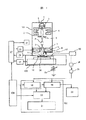
本発明の第1の実施例を図1と図2により説明する。図1および図2は本発明の構成図である。
【0032】
検査装置は大別して電子光学系101,試料室102,制御部104,画像処理部105より構成されている。
【0033】
電子光学系101は電子源1,電子線引き出し電極2,コンデンサレンズ4,ブランキング用偏向器17,走査偏向器8,絞り5,対物レンズ7により構成されている。図1には2次電子検出器9が対物レンズ7の下方にある場合を示したが、検出器9の位置は対物レンズ7の上に設けても良い。その場合は二次電子が対物レンズ7の中を通過してから検出器9に到達する。検出器9が対物レンズ7の下部にある場合は対物レンズ7の偏向範囲が大きく取れるが対物レンズ7の収差が大きいためレビュー時の分解能に限界がある。一方、検出器9を対物レンズ7の上に設けた場合は、対物レンズ7の収差を小さくできるためにレビュー時の分解能をより上げることが可能であるが偏向範囲が小さくなるという欠点があるので両者は一長一短であり必要に応じてどちらかの構成を選択すればよい。検出器9には正の高電圧が印加されている。さらにその検出器9につながるプリアンプ12および検出回路30のグランドレベルも検出器9に印加した正の高電位の上に乗っている。二次電子検出器9の出力信号はプリアンプ12で増幅され検出回路30によりデジタルデータとなる。 この信号は光発信器34により光に変換され、グランド電位レベルにある光受信機35によって光を受信し電気信号に変換した後に画像処理部105に送られる。
【0034】
図1では、コンデンサレンズ4を電磁レンズで構成したが、図2のように静電レンズで構成しても良い、静電レンズは例えば3枚の電極から構成され、両側の電極はグランド電位とし中央の電極に正または負の電圧を印加する、いわゆるアインツェルレンズが最適であるが、特にアインツェルレンズでなくとも同様である。静電レンズを使用することで電子光学系を小型化できる。
【0035】
図1に戻って、試料室102は、ステージ24,光学式試料高さ測定器29,レーザ測長器またはリニアスケールを用いたステージ位置測定器31により構成されている。
【0036】
画像処理部105は、画像記憶部18,19,演算部20,欠陥判定部21より構成されている。取り込まれた電子線画像は、モニタ22に表示される。検査装置各部の動作命令および動作条件は、制御部104から入出力される。予め制御部104に電子線発生時の加速電圧,電子線偏向幅,偏向速度,試料台移動速度,検出器の信号取り込みタイミング等々の条件が入力されている。また、光学式試料高さ測定器29の信号やステージ位置測定器31の信号から補正信号を生成し、電子線6が常に正しい位置に照射されるよう対物レンズ電源7や走査信号発生器13に補正信号を送る。
【0037】
図3は電子ビームによる半導体のパターン外観検査のフローを示す図である。この図を用いて本発明により半導体ウェハのパターン外観検査を実施するフローを説明する。
【0038】
まず、ウェハをロードした後、光学顕微鏡により粗いアライメントを実施する。これは,電子線走査画像では走査範囲が狭く、ローディング時の機械的な位置決めだけではアライメントマークが電子線の走査範囲内に入らない可能性があるからである。そこで、視野の広い低倍率の光学顕微鏡によりおよそ数十μmの精度でアライメントを行う。
【0039】
次に電子光学系の条件設定を実施する。検査するウェハのパターンの種類により電子ビームの照射エネルギーや画素サイズ(画像の最小要素),ビーム電流等を設定する。パターンの材質に依り最適な電子ビームの照射エネルギーが異なる。通常、導電性材料では高分解能が得られるように数keV以上の高目のエネルギーとし、絶縁物を含むパターンでは帯電防止のために1.5keV以下に設定すると良い。
【0040】
次に特に注目したい欠陥サイズに応じた画素サイズを設定する。無意味に画素サイズを小さくすると検査所要時間が増大してしまう。次にビーム電流を設定する。デフォルトの値は装置固有に存在するが、特に帯電しやすいウェハでは小さめの電流に設定すると良い。又、検出したい欠陥のコントラストが大きいことが予めわかっていれば、電流を小さめにして電子ビームをより小さく絞り高感度の検査ができる。
【0041】
次に、検査するウェハの電子線による画像を表示させ、焦点や非点収差の補正を実施する。これは画像を取り込んで計算機上またはそれ専用の画像処理装置を用いて自動で実施することも可能である。
【0042】
以上の設定が終了したらつぎに電子ビームによる画像の精アライメントを実施する。これによりステージの座標系とウェハの座標系が正確に一致し、ステージの座標をレーザ測長機等により計測することでウェハ上の所望の位置を検査することが可能となる。
【0043】
次に、検査したいエリアを制御用ワークステーションのディスプレー等の制御用画面から入力する。
【0044】
次に試し検査を実施する。試し検査とは上記で設定した各種パラメータが適当であるかを判断するために実施する。まず検査したいパターンの一部分を指定する。これが試し検査の領域指定である。そして試し検査を実施する。試し検査では電子ビームにより本番の欠陥検出検査と同様の動作により画像を検出するが、画像処理回路を通すことなく取得した画像をメモリにすべて取り込む。
【0045】
次に、画像処理条件の設定を行う。この条件は、画像処理装置が、隣接する同一パターンの二つの画像を比較するときに、欠陥であるか否かを判断する閾値である。この閾値を低く設定すると欠陥検出感度は向上するが欠陥でない部分を欠陥と見なしてしまう可能性が大きくなる。一方、閾値を上げると検出感度は低下していく。
【0046】
図3において、明るさ閾値とは、二つの画像の輝度信号の差の閾値である。電子ビームによる画像は光学顕微鏡画像に比べてざらつきが大きい(すなわち画像のSN比が悪い).したがって、比較している検査対象物が同じもので、平均的な明るさが同一でも、画素毎に見るとやや明暗のばらつきが存在する。したがって明暗差の閾値を設け、画像を比較してその閾値より大きく明暗の差が生じた場所のみを欠陥として検出することで画像のざらつきを欠陥と認識しないようにしている。
【0047】
又、位置ズレ閾値とは、比較する二枚の画像の位置あわせの不完全さを欠陥と誤認識しないようにする為に設ける。画像の位置ズレがここで設定した閾値程度は存在すると見做してそれ以上の差が生じた場合のみを欠陥とする。
【0048】
フィルタ種類とは、取得した画像に施すフィルタであり、検出した画像のざらつきを軽減したりエッジを強調するために存在する。これはパターンの種類や検出したい欠陥に応じて最適なものを試行錯誤で選択する。
【0049】
以上のパラメータを設定した後、画像処理を実施する。試し検査における画像処理では,すでに取得した一連の画像を用いて比較検査を行う。この検査により欠陥が検出され、その座標が記憶され、制御画面上に欠陥の場所を表示する。この時点で一つも欠陥が検出されない場合、上記画像処理パラメータの閾値を下げて感度を上げて再びメモリ上の2次元情報を用いて比較検査を実施する。
【0050】
次に、試し検査で検出された座標の画像を観察する。これがレビューである。すでにその部分の画像はメモリに記憶されているので、まずその画像を制御用ワークステーションのディスプレーや画像表示専用のディスプレー等に表示し目視でどのような欠陥が検出されたかを観察する。ここでかなり大きな欠陥については目視により簡単に欠陥の形状や種類とが判明する。しかし、装置の性能限界に近い微細な欠陥や、コントラストの小さい欠陥は、目視では充分に明確に判定できない場合が多い。そこで、電子光学系の条件をレビューの条件に切り替えて高分解能の像を表示する。これにより、試し検査で検出した欠陥が、真の欠陥であるかまた検出したかった欠陥であるかを容易に判別できる。その結果から、画像処理のパラメータを再設定し、再びレビューすることを繰り返すことで検出したい欠陥を確実に検出できる条件を見いだすことができる。
【0051】
高分解能のレビュー条件が存在しない従来の装置では、大電流の電子ビームにより画像を形成するように設計されており、長時間観察すると試料に電子ビームが大量に照射され,試料が破壊したり帯電により画像を観察できなくなったりする。また、欠陥の有無を確認するのが目的であり、目視観察により欠陥の詳細を判断するには分解能が不十分である。そのため、このレビューと画像処理パラメータ設定において試行錯誤を繰り返さざるを得ず多大な時間を要していた。ところが本発明によれば、レビュー画面の質が良いために画像処理パラメータの選択の良否が正確に判断でき、試行錯誤の回数が格段に減少した。これにより有人作業の時間が大幅に短縮され、総合的な装置稼働効率も向上した。
【0052】
条件設定のためのレビューが終了したら欠陥検出検査を開始する。この欠陥検出検査は無人で自動的に行われる。この欠陥検出検査が終了したら再びレビューを実施する。このレビューにより検出された欠陥が真の欠陥であるかを確認した後にウェハをアンロードする。必要であれば他の分析検査装置へ移動し、各種検査分析を行う。
【0053】
すでに欠陥検出検査条件の確立しているウェハを自動的に検査する場合には、図4のようなフローで欠陥検出検査とレビューを実施する。すなわち、ウェハをロードしたらすぐに既存の条件設定で欠陥検出検査を実施し、欠陥検出検査の終了後にレビューを実施する.このレビューでは、検出した欠陥を異物,電気的な欠陥,形状不良等の欠陥の種類を見極めて欠陥毎に分類する。
【0054】
次に、本発明のポイントとなるレビュー条件と、欠陥検出検査条件の仕様,相違点と特徴について説明する。
【0055】
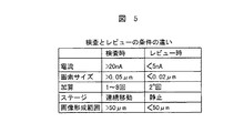
欠陥検出検査条件とレビュー条件の性能を比較したものが図5である。
【0056】
欠陥検出検査条件は、ウェハ全面の検査を実用的な時間で実行するために非常に高速な画像取得が可能である。すなわち画素サイズ0.1μmで100μm角を画像形成する時間は20msec以下となっている。高速画像取得のためにステージは連続的に移動しており電子ビームはそのほぼ直交方向に走査されるようになっている。さらに高速にかつ検査に耐え得るSN比の画像形成を実現するためにビーム電流を20 nA以上得られるように設計した。具体的には、まず電子源から得られる電流密度を0.2 mA/sr以上とした。さらにレンズの絞りを高分解能SEMと比較して大きいものを用い、電子源からの電子ビームの取り込み角α(すなわち、電子源から広い角度を持って放出する電子ビームのうち試料に照射される電子ビームの開き角)を6 mrad以上とした。画像の最小単位である画素サイズは、検出したい最小の欠陥サイズと同等とした。現状では問題となる最小の欠陥はほぼ0.05μmであることから画素サイズは0.05μm以上とした。ここでの0.05μm以上という意味はウエハによっては0.05μmより大きな欠陥サイズを見る場合も有るため画素サイズは0.05μmより大きく設定出来るようにしてあることを示すために記載した。又、被検査ウェハの工程によっては二次電子の発生量が小さく一回の電子ビーム走査だけでは充分な明るさが得られない場合がある。その場合には電子ビームを複数回走査して得られた画像を加算することも可能である。ただし検査時間が遅くなる問題があるため加算回数は少ないほど良い。又、画像形成範囲は極力大きい方が良い為50μm以上とし、100μmを標準とした。
【0057】
一方、レビュー条件では、画像形成にそれほど高速性を要求されないため電流値が大きい必要はなく5nA以下で充分である。画素サイズは欠陥の形状を詳細に観察するため欠陥の大きさの1/5以下は必要である。したがって0.02μm以下とした。また画像の加算は2のn乗回とし、特に回数の上限はない。レビューでは、ある特定の場所をじっくりと観察するためステージは静止させ電子ビームを二次元に走査させる。さらに欠陥を拡大してみるために画像形成範囲は小さい必要があり50μm以下である。
【0058】
以上を整理してみると、検査の場合とレビュ-モ-ドの場合では画素サイズの考え方に大きな違いがあり、検査の場合は欠陥サイズより大きなプロ-ブサイズであってもそこに欠陥が有るか無いかを判断すれば良い。即ちプロ-ブサイズと画素サイズとが同等もしくはそれ以上大きければ良い。画素サイズが小さければ単位面積に照射される電子の量が小さくなるため長い時間照射するためクロックが遅くなるため高速に検査が出来ないという問題が有る。これに対し、レビュ-時にその欠陥の像を採取するため時間をかけて少なくとも欠陥サイズの1/5以下のプロ-ブを必要とするものである。この発明は検査時とレビュ-時でプロ-ブサイズを変更すると共に画素サイズも合わせて変更することにある。
【0059】
次に具体的に、欠陥検出検査条件とレビュー条件をどのようにして切り替えるかを説明する。
【0060】
最初に電子光学系の構成要素とその動作の詳細について、図1を用いて説明する。電子源1には、電界放出電子源、特に拡散補給型の熱電界放出電子源が好ましく、タングステンチップにジルコニウム及び酸素とからなる被覆層を設けた、所謂Zr/O/W型電子源を用いた。この電子源は長時間安定な電子放出が可能である。しかも引出電圧を変えることで放射角電流密度を0.001mA/sr〜1mA/srの範囲で自由に設定できる。ただし電流密度を大きくすると放出電子のエネルギー幅も増大するので色収差が増大する。検査時には電子ビーム電流を20nA以上得る必要があった。そこで電子源1からの放出電子ビームの放射角電流密度は0.2〜1mA/Srの範囲で用いる。電子ビーム6は引出電極2に電圧を印加することで電子源1から引き出される。電子ビーム6の加速は電子源1に高圧の負の電位を印加することでなされる。加速電圧を10kVまたはそれ以上を設定できるようにした。これは大電流電子ビームを使用するために上述した電子ビームのエネルギー幅増大による色収差を抑制するためと,大電流電子ビームが電子の相互作用で広がってしまい絞れなくなる現象(クーロン効果)を抑制するためである。電子線6は約10kVに相当するエネルギーでステージ24の方向に進み、コンデンサレンズ4で収束され、さらに対物レンズ7により細く絞られステージ24の上に搭載された被検査基板10(ウェハあるいはチップ等)に照射される。偏向領域を50μm角以上とし周辺部においても歪みのない画像を取得するために、対物レンズ7と被検査基板10の距離(動作距離)を25mmとした。その結果、対物レンズ7の焦点距離は約30mmと長くなっている。
【0061】
被検査基板10には高圧電源25により負の電圧を印加するための負電圧印加手段がある。この高圧電源25を調節することにより被検査基板10への電子線照射エネルギーを最適な値に調節することが容易となる。例えばこの電圧を-9.5kVとし、電子ビームの加速電圧が10kVであれば試料への照射エネルギーは500eVとなる。
【0062】
画像形成には、電子ビーム6は一次元のみ走査し走査方向と直交する方向にステージ24を連続的に移動する方法を採用した。
【0063】
画像形成のための信号検出は以下のように行われる。すなわち、試料10に照射された電子ビーム6により二次電子が発生する。この二次電子は試料10に印加された電位により急激に加速されるために検出器9に直接引き込むことは非常に困難である。そこで被検査基板10と検出器9の間に電界と磁界を組み合わせた偏向器たとえばExB偏向器14と加速された二次電子を低速の二次電子に変換する変換電極11を設ける。
【0064】
ExB偏向器14は電界と磁界が直交した偏向器であり、上部からExB偏向器14へ入射してくる一次電子ビーム6に対しては、磁界による偏向作用と電界による偏向作用とが逆方向でキャンセルするようになっており、下部からExB偏向器14へ入射してくる二次電子に対しては磁界による偏向作用と電界による偏向作用とが加算されるようになっている偏向器である。
【0065】
二次電子は、このExB偏向器14により偏向を受けた後、変換電極11に照射される。そして変換電極11から発生する二次電子を検出器9により検出する。検出器9には、10nA以上の大電流高速検出を実現するためにPIN型半導体検出器を用いた。ここで検出された二次電子信号はプリアンプ12により増幅され、検出回路30によりAD変換され、二次電子信号から得られた、試料の二次元像に対応するデータを記憶する画像記憶部18または19に送られる。ステージ24の移動により被検査基板10を移動し、電子源1である電界放出陰極からの電子ビーム6を被検査基板10に照射し放出された二次電子信号を用いて比較検査を実行する。
【0066】
上記方法により、半導体パターンの数μm離れて隣接する同一パターンの繰り返し部分の画像を演算部20や欠陥判定部21にて高速に比較判定することで欠陥が検出される。又、異なるチップの同一パターン部のチップ同志の画像比較を実施することでも欠陥を検出できる。
【0067】
次にレビュー条件へ切り替える方法について説明する。
【0068】
欠陥検出検査条件において分解能を制限している要因は主に、1)エネルギーのばらついた電子をレンズでフォーカスすることにより発生する色収差,2)電流密度が高いため電子が反発し合うことにより生じるクーロン効果,3)電子源の先端が点光源でないことで生じる有限の光源径,以上の3つである。レビュー条件への切り替えの基本的な考え方は、電子ビーム電流を欠陥検出検査時よりも下げることで光学系の収差やクーロン効果といった電子ビームを小さく絞ることを阻害する要因を抑え、微小なビームを形成し、それにより高分解能画像を得ようとするものである。具体的な方法を以下に列挙する。
【0069】
第1は、電子源から引き出す電流密度を下げる方法である。電子銃の構成図を図6に示す。電子源1は、タングステンチップにジルコニウム及び酸素とからなる被覆層を設けた、所謂Zr/O/W型ショットキ−電子源である。電子源1のフィラメントは加熱電源405により電流を流すことで加熱される。不要な熱電子を抑制するためのサプレッサ電極403の中央の穴から電子源1の先端が突出している。サプレッサ電極403には電子源1に対してマイナスの電位がVs電源407により与えられている。電子源1の先端は引出電極2に対面しており、引出電極2には電子源1に対してプラスの電位が引出電源406により印加されている。各電源405,406,407は加速電源408により所望の加速電圧分だけマイナスにフローティングされている。この結果、電子源1から引き出された電子ビームはグランド電位のアノード電極404までの間に加速される。以上の構成の電子銃において引き出される電子電流密度を低減するには電子源先端の引出電界を低減させればよい。それにはサプレッサ電極403に接続される電源407の電圧値を大きくする方法と引出電極2の電位を下げる方法で実現できる。
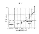
【0070】
次に、電流密度を下げることで収差が低減できる理由を説明する。図7は電子源から放出される電子の放射角あたりの電流密度とそのビームのエネルギ−のばらつきの半値幅(エネルギ−幅と呼ぶことにする)を示したものである。エネルギ−幅は電子光学系のレンズの色収差の原因となり、その関係は数1のようにエネルギ−幅と色収差が比例する。そのためエネルギ−幅が1/2になれば色収差も1/2になる。欠陥検出検査条件では放射角電流密度は0.1 mA/sr〜1 mA/srで使用し,レビュー時では0.001〜0.01 mA/srで使用する。これによりビーム電流は、欠陥検出検査時は約100nAで、レビュー時は約5nA以下となり、エネルギー幅は図7より1/3になり色収差も1/3になる。その結果ビーム径も1/3程度になり分解能が向上する。
【0071】
【数1】

電流を低減して分解能を向上させる第2の方法は、絞り(例えば図1の絞り5)の直径を小さいものに交換して収差を低減する方法である。数1のように光学系の色収差はビームの開き角αに比例している。したがって、ビームの開き角を決定する絞りの直径を1/2にすれば色収差も1/2となる。開き角を小さくしすぎると開き角に反比例する回折収差が増大するが、1 mrad程度以上の開き角であれば回折収差は問題とならないのでビームの直径もほぼ1/2になる。ただしこの方法は機械的な絞りの移動機構が必要となり信頼性や簡便さといった点から問題が多い。
【0073】
第3の方法として、レンズの焦点距離を変えて光学系の倍率を変化させることで、絞りを移動させることなくビームの開き角を小さくする方法を説明する。これにより電子源の光源の大きさも縮小できるため第2の方法より優れたものである。これを図8により説明する。電子源から放出された電子ビームは欠陥検出検査条件ではコンデンサレンズにより一度焦点(クロスオーバと呼ぶ)を結び、対物レンズにより再び試料上に焦点を結ぶ。一方、レビュー時にはコンデンサレンズのレンズ作用をゼロにすることで電子源からの取り込み角αが狭くなり、しかも対物レンズの照射角βも狭くなる。これによって電流値の低下とともに対物レンズの色収差が低減され分解能が向上する。しかも、欠陥検出検査時の光学系全体の倍率は (b/a)*(d/c)であったものが、レビュー時には d/(a + b + c) と小さくなるため電子源の光源を縮小できることにもなり、分解能はさらに向上する。コンデンサレンズは電磁レンズを使用しておりコイルと磁路から構成されている。レンズ作用の強弱はコイルに流す電流値で制御できるためレンズ作用をゼロにする場合は電流をゼロにすればよい。また、コンデンサレンズの作用をゼロにする場合について説明したが、完全にゼロにしなくてもクロスオーバが形成されない程度の弱いレンズ条件とすることで同様の効果が期待できる。
【0074】
また、コンデンサレンズの強度を欠陥検出検査時よりも強くし、クロスオーバの位置を絞りより上に移動させることでも分解能を向上させることが可能である。これを図9に示した。得られる効果はコンデンサレンズのレンズ作用をゼロにした場合と同様である。すなわち光学系の倍率は (b/a)*(d/c)で表わされ、図8と図9を比較すれば分かるように欠陥検出検査時に比べてbが小さく、cが大きくなるため倍率は小さくなる。また照射角βを小さくできる。
【0075】
以上ではビーム電流を減少させることでレビュー時に高分解能の画像を形成する手法について説明した。一方、ビーム電流を減少させると、検出器で検出できる信号が非常に減少する。したがって、検出系の増幅率が欠陥検出検査時と同一であると入力信号が検出回路30の最小ビット以下になってしまい、電子ビームを複数回試料上に走査して画像の加算を実施しても良好な画像が得られないことになってしまう。
【0076】
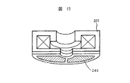
そこで、プリアンプからADコンバータヘ入力するまでの回路をもう一式用意した。すなわち、図1における検出回路30の中に信号経路を2系統設けるものである。その構成を図15に示す。欠陥検出検査時には検出器9からの信号が低ゲインアンプ301を経由してA/Dコンバータ304へ直接入力する。一方、レビュー時にはビーム電流値が減少するので検出器9からの信号が低下する。その分だけゲインの高い高ゲインアンプ302の方に信号経路を切り替えるようにする。さらに高域カットフィルタ303を経由してADコンバータ304に入力する。欠陥検出検査時とレビュー時の信号波形の模式図である図16を用いて、この回路の動作を説明する。
【0077】
欠陥検出検査時のビーム電流が100nA、レビュー時のビーム電流が500pAの場合を例に採って示す。低ゲインアンプ301と高ゲインアンプ302のゲイン比率をビーム電流の比と等しい200とした。その結果、両者のアンプの出力の平均値は等しくなる(任意単位100)。図16(a)は半導体の無パターン部について画像形成した場合の欠陥検出検査時の信号波形であり、大電流ビームを用いているためノイズ振幅は小さい。一方、図16(b)は同一部のレビュー時の信号波形である。信号の平均はほぼ100であるが、わずかな信号を高いゲインで増幅しているためにノイズが大きく−100〜300まで振れることになる。マイナス側にアナログ信号が変動した場合、デジタル化された値はゼロとなる。また大きすぎてもA/Dコンバータのフルスケールを越えてしまう。したがってデジタル信号を加算平均しても正確な波形が得られないという問題が生じる。これを解決するために高ゲインアンプの後段に高域カットフィルタ303を置いた。A/Dコンバータ304への入力信号は図16(b)の「フィルタ処理あり」の波形のようにノイズが低減される。さらにこの波形をデジタル化した後、電子ビームの走査を複数回行ってその信号を加算すれば、充分なSN比を持った画像信号を得ることが可能となる。
【0078】
以上で分解能を向上する3つの方法とビーム電流を減じたことで発生する問題を解決する方法を説明した。本実施例では分解能を向上するために、主にコンデンサレンズの励磁条件を変化させる第3の方法を用い、電子源から引きだす電流値を可変する第1の方法を補助的に用いることとした。以下に具体的な数値例を示す。
【0079】
欠陥検出検査時は、電子源からの放射角電流密度を0.5mA/srとして、光学系の倍率を1倍、ビーム電流は100nAとした。この時の画像の分解能は0.08μm程度であった。この時のライン・アンド・スペース パターンの画像のラインプロファイルを図10に示す。
【0080】
レビューでは、コンデンサレンズ電流値を増大させ、倍率を0.2とした。さらに、電子銃の高圧電源を制御し、電子源からの放射角電流密度を0.1mA/srに下げた。その結果、ビーム電流は500pAに減少したので検出系のプリアンプのゲインを200倍に切り替え、周波数特性を約1/10にするフィルタを通過するようにした。電子ビームの走査速度は欠陥検出検査時の約1/10とした。さらにSN比の劣化を補償するために画像加算を64回実施するようにした。この時の画像の分解能は0.02μm程度であった。このときの画像のラインプロファイルを図10に重ねて示す。レビュー時のラインプロファイルの立上りが鋭くなっており、しかも振幅も大きくなっているのがわかる。このことから明らかに分解能が向上し、細かい物体まで観察可能であることが確認できる。
【0081】
(実施例2)
実施例1では、レビュー時と欠陥検出検査時で同一の検出器を用いていた。しかし、レビュー時には検出信号が激減するために電流の減少した割合だけプリアンプ12のゲインを200〜1000倍にする必要がある。さらに、周波数特性が欠陥検出検査時の様に高いままゲインだけを増倍すると回路が発振したり、回路のノイズ振幅が平均信号量より大きくなってしまう問題がある。そのために高周波をカットする回路を付加する必要があり、回路が複雑となる。その結果、欠陥検出検査時の検出信号にノイズが混入したり周波数特性が劣化したりする可能性がある。それを解決するために、本実施例ではレビュー時専用の検出器を設けることにした。その構成図を図11に示す。欠陥検出検査用検出器9の電子ビームの光軸に関してほぼ対称な位置にレビュー用の検出器を設けた。この検出器は通常の走査電子顕微鏡に用いられているもので、シンチレータ52と光電子増倍管51で構成されている。応答特性はDC〜20MHzである。試料10から放出された二次電子はExB偏向器14により欠陥検出検査時には欠陥検出検査用検出器9の方向に、レビュー時にはレビュー用検出器の方向に偏向される。この二次電子は、それぞれの検出器に対面した変換電極に照射され、それによって放出された二次電子を検出する。シンチレータ52の前面にはプラスの高電圧を電源53により印加し、二次電子を加速して衝突させ、光に変換する。その光を光電子増倍管51により増倍して検出する。二次電子の偏向方向の切り替えはExB偏向器14の制御電源31の極性を逆(印加電圧と偏向コイル電流の極性を反対にする)にすることで達成される。これに連動していずれか一方の検出器からの信号をメモリ18経由でモニタ22に表示する。これらの切り替えは制御部104が行う。
【0082】
(実施例3)
欠陥の種類によってはレビューの条件を適切なものにしないと検出した欠陥コントラストが消滅してしまう場合がある。例えば、導通孔の導通不良欠陥のなかには複数回ビームを照射しているうちに欠陥のコントラストが消えてしまうような場合がある。したがって,そのような欠陥をレビューするときは画像の加算回数を制限する必要がある。加算回数が制限されるため、SN比の良好な画像を得るためにはビーム電流を大きめにする必要がある。また欠陥の種類によっては、欠陥検出検査時の大電流ビームではリターディング電界(検査ウェハに印加される電子ビーム減速用の電界)が強い方が欠陥部のコントラストが大きいが、小電流時にはリターディング電界を弱くする方がコントラストが強調されるものも存在する。以下では、導通不良欠陥をレビューする場合の条件設定方法を一例として説明する。
【0083】
半導体のプロセスには上層と下層の間の縦方向の導通を取るために、穴をあけその中に導電性の材料を埋め込む工程がある。この孔あけや埋込みに不良があると完全に電気的にオープンとなったり、非常に高い抵抗値になったりする。このような工程を欠陥検出検査すると、導通のある孔は明るく、非導通の穴は暗くなる。さらに不良すれすれの微妙な高抵抗値の場合、中間的な明るさとなるため完全な導通のある孔と比較することで欠陥として検出される。このような欠陥はレビュー時に電流を絞って画像加算を数十回実施すると、完全に導通している孔と同じ明るさになってしまいレビューしてもなんら情報が得られないことが多い。そこで、導通孔を欠陥検出検査する場合には、検出した欠陥毎に明るさのレベルを欠陥座標と組み合わせて記憶しておき、グレーの欠陥をレビューする場合には自動的にビーム電流を5nA以下にならないように光学条件を設定し画像加算回数を10回以下に抑えた。一方、非常に暗いレベルの欠陥をレビューする場合にはビーム電流を極力下げ、500 pA以下の条件でレビューを実施した。
【0084】
以上は一例であり、要は、欠陥検出検査時の画像から得られる情報、すなわち明るさ,欠陥の大きさ,形状等を用いて自動的に欠陥の種類を分類し、それぞれに応じたレビュー用の光学条件すなわち走査範囲,ビーム電流,走査速度,画像加算回数を自動的に対応付けるようにする。このとき、本発明では光学条件の変更に機械的な移動すなわち絞りの移動等を極力伴わないようにしたため、それぞれの欠陥毎に瞬時に条件を切り替えられるようになった。
【0085】
(実施例4)
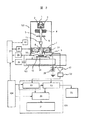
本発明の第4の実施例としてレビュー用の電子光学系を欠陥検出検査用の電子光学系から独立のものにした。これを図12により説明する。図12は本実施例の構成図である。
【0086】
検査装置は大別して欠陥検出検査用電子光学系101,レビュー用電子光学系200,試料室102,制御部104,画像処理部105より構成されている。レビュー用電子光学系200以外は実施例1と実質的に同一である.
レビュー用電子光学系は電子源201,電子線引き出し電極202,コンデンサレンズ204,走査偏向器208,絞り205,対物レンズ207により構成されている。また2次電子検出器209が対物レンズ207の上方にあり、二次電子検出器209の出力信号はプリアンプ212で増幅され低速画像表示回路218に送られる。
【0087】
試料台24にはリターディング電圧が印加されるが、欠陥検出検査用光学系101の下からレビュー用電子光学系の下にステージが移動する際には、ステージの構造によりリターディング電圧を一度遮断してから移動する方が好ましい場合もあるので、印加するリターディング電圧や被検査基板の種類により選択すればよい。
【0088】
次に、本実施例のポイントとなるレビュー用電子光学系と欠陥検出検査用光学系の仕様,相違点と特徴について説明する。
【0089】
欠陥検出検査用の電子光学系101はウェハ全面の検査を実用的な時間で実行するために非常に高速な画像取得が可能である。すなわち画素サイズ0.1μm以下で100μm角を画像形成する時間は20 msec以下となっている。高速画像取得のためにステージは連続的に移動しており電子ビームはその直交方向に走査されるようになっている。さらに高速にかつ検査に耐え得るSN比の画像形成を実現するためにビーム電流を20nA以上得られるように設計した。具体的には、まず電子源1から得られる電流密度を、安定に得られる限界値である約1 mA/srとした。これは高分解能SEMの約20倍である。さらにレンズの絞りを高分解能SEMと比較して大きいものを用い、電子源1からの電子ビームの取り込み角α(すなわち、電子源1から広い角度を持って放出する電子ビームのうち試料10に照射される電子ビームの開き角)を約20倍とした。
【0090】
また、画像の周辺部が歪んだり分解能が中心部と比べて低下したりすると検査感度が不均一になるために、電子ビームの走査領域に余裕を持たせる必要がある。そこで対物レンズの焦点距離や動作距離が通常の高分解能SEMに比べかなり長いものを採用した。
【0091】
又、電子ビームの試料照射開き角βが大きくなると焦点深度が浅くなってしまう。βは光学系全体の倍率Mでαを割ったものとなるため、倍率Mはあまり小さくすることができない。したがって、高分解能SEMにくらべてかなり大きい倍率となっている。
【0092】
以上の設計により、欠陥検出検査に必要な分解能を確保した上で高速性に必要な大電流を得られるものとなっている。この電子光学系は以上の説明にあるように単純に電子ビーム電流を減じたとしても高分解能SEMと同様の分解能が得られないことは光学系の倍率、対物レンズの焦点距離や動作距離からも明らかである。
【0093】
一方レビュー用の電子光学系では高速性はさほど重要ではない。また観察したい場所の座標が正確にわかっているので視野は20μmあれば充分である。したがって電子ビーム電流は小さくて良い。しかも対物レンズの焦点距離や動作距離も短くて良いこと、また光学系の倍率を小さくできることにより通常の高分解能SEMと同様の高分解能画像を取得できる。
【0094】
次にレビュー用の電子光学系200について述べる。電子源201には欠陥検出検査用電子光学系と同様の拡散補給型の熱電界放出電子源であるZr/O/W型電子源を用いた。電流密度を大きくすると放出電子のエネルギー幅も増大し色収差が増大する。レビュー用電子光学系ではビーム電流は100pA以下で良いので放射角電流密度は0.05mA/Sr以下で用いることとした。これにより電子ビーム206のエネルギー幅は欠陥検出検査用電子光学系の場合に比べ約1/3〜1/4に減少し、色収差もそれだけ減少することになる。電子線206は引出電極202に電圧を印加することで電子源201から引き出される。電子線206の加速は電子源201に高圧の負の電位を印加することでなされる。レビュー用光学系200では加速電圧を500V〜10kVまで可変できるようにした。レビュー用光学系200では電流が小さくて良いため、上述のように色収差が小さくまたクーロン効果も無視できる。したがって、低い加速電圧で十分小さいビーム径を得られるので標準では加速電圧2kVに設定した。電子線206は2kVに相当するエネルギーで試料台24方向に進み、コンデンサレンズ204で収束され、さらに対物レンズ207により細く絞られステージ24の上に搭載された被検査基板10(ウェハあるいはチップ等)に照射される。対物レンズ207は被検査基板10に非常に接近させており、動作距離は5 mmとした。対物レンズ207の焦点距離は8mmである。これにより収差の小さい対物レンズを実現できた。分解能は殆ど色収差により決まっている。したがって欠陥検出検査用の対物レンズに比べて収差係数は約1/4で電子ビームのエネルギー幅が欠陥検出検査用光学系の約1/3であることから、分解能は約1/12となる。被検査基板10は欠陥検出検査用とレビュー用とで共通であり、したがって高圧電源25により負の電圧を印加できる。この高圧電源25を調節することにより被検査基板23への電子線照射エネルギーを最適な値に調節することができる。照射エネルギーを変えることによりコントラストの異なる画像が得られるため、欠陥が形状相違によるのか材質によるものであるか、または電気的な導通によるものなのかなどの情報を多角的に得ることができる。
【0095】
画像形成には電子ビーム206を二次元に走査する。すなわちステージ24は固定とする。被検査基板10に照射された電子ビーム206により発生する二次電子は欠陥検出検査用光学系101と同様に被検査基板10に印加された電位により加速される。対物レンズ207が被検査基板10に約30mm以下と非常に接近しているために検出器209は対物レンズ207よりも上方に設けてあり、二次電子は対物レンズ207の中心を通過させる。欠陥検出検査用光学系101と比べて被検査基板10に印加する電位は低いため二次電子のエネルギーは弱いが検出器209に直接引き込むことはやはり困難である。そこで変換電極211に照射させ、そこから放出する二次電子を検出器209により検出する。検出器209には通常のSEMに使用されている、蛍光体と光電子増倍管を用いた検出器209を用いた。ここで検出された二次電子信号はプリアンプ212により増幅およびAD変換器230でAD変換され、画像観察用のモニタ22に表示するとともに必要に応じて画像ファイルとしてディスク等の外部記憶装置219に記憶させたりプリントアウトできるようになっている。
【0096】
以上で第4の実施例について説明したが、各機能の数値は一例である。要は欠陥検出検査用の電子光学系とくらべて約1/10程度のビーム径を達成できるレビュー用の電子光学系を欠陥検出検査用電子光学系と同一の試料室上に並べて配置すること、そして試料台の平行移動のみで迅速に欠陥検出検査とレビューの動作を切り替えられるようにすることが本実施例の本質である。
(実施例5)
第5の実施例は、第4の実施例のレビュー用電子光学系200の対物レンズ207の下磁路にX線検出器240を組み込み、電子ビーム照射により発生する特性X線を検出できるようにした。これによりEDX(Energy-Dispersive X-ray)分析が可能となり、レビュー時に欠陥の材質を特定することが可能となった。図13は中心に穴の空いたアニュラー型のX線検出器を組み込んだ場合の対物レンズ付近の図である。
【0097】
また対物レンズの動作距離を第1の実施例よりもやや大きくしてX線分析器を対物レンズと試料の間に挿入しても良い。
【0098】
(実施例6)
電子ビームによる検査では、形状の欠陥だけでなく電気的な導通、非導通の検査が可能である。導通している部分は帯電せず、非導通部分のみが帯電することにより発生する二次電子のエネルギーや軌道が変化し、画像の明るさが異なるからである。これは、大電流電子ビームの照射により特に大きなコントラストとして発生する。ところがレビュー用電子光学系では電流が小さいために帯電の差が小さく、コントラスト差として現れにくい。そこで、二次電子のエネルギーのわずかな差でも高感度にフィルタリング可能な二次電子エネルギーフィルタを設けた。エネルギーフィルタは対物レンズの上に設けた。この分析器の図を図14に示す。半球状のメッシュ220が対物レンズ207上方に二次電子軌道を遮るように設けられている。メッシュ220の中央には一次電子ビーム206が通過する穴が開けられている。このメッシュ220には電源221により被検査基板10の電位よりも±20V程度の範囲の電位を与える。これにより被検査基板の帯電の状況を画像化することができる。二次電子は放出した場所の電位φを基準として約2eVをピークとするエネルギー分布を持っている。したがって、グランド電位から見た二次電子のエネルギーのピークは(−φ+2)eVとなる。例えば被検査基板10にリターディング電位が500V印加されているとすると、二次電子エネルギーのピークは502eVとなる。もし、一次ビーム照射位置が本来、基板10と導通すべき場所であるにも関わらずその部分だけパターン欠陥により非導通の場合にはその部分がマイナスに帯電する。するとそこから放出される二次電子のエネルギーは帯電した電圧だけ高いことになる。帯電電圧を5Vとすると、507eVである。そこでメッシュ220に-505Vを与えれば、帯電していない部分からの二次電子の大部分は上記メッシュ220を通過することはできない。したがって帯電している部分のみが明るく見えることになる。このようにしてわずかな帯電もコントラスト差として得ることができる。ここではマイナスに帯電する場合のみを説明したが実際の半導体においては電子ビーム照射による帯電のメカニズムは複雑であり、正に帯電する場合もある。その場合にはメッシュ220に与える電位をリターディング電位と同電位またはややプラスとすればよい。その場合は正に帯電するところが暗くその他の部分は明るくなる。
【0099】
本実施例のエネルギー分析器の分解能は約0.1V程度を得ることができる。したがって、レビュー時には電子ビーム電流が小さいために欠陥部の帯電量が小さくても電位によるコントラストが強調されるため欠陥の特定が容易に可能である。
【0100】
【発明の効果】
本発明は、以上説明したようなものであるから、以下に記載されるような効果を奏する。 比較的大面積の領域に亘って欠陥の存在を検出する為の高速画像取得による欠陥検出検査と、この欠陥検出検査により検出された特定の狭い部位を画像化し肉眼で観察するレビューとを、夫々独立に最適化された経路を備えた検出回路で介して行うことにより十分なSN比を持った画像信号信号を得ることが可能となり、検査条件を効率よく設定することが可能となった。これにより検査工程の高速化と共に検査結果の信頼性が向上した。
【0101】
また、欠陥の存在を検出する欠陥検出検査の為の第1の電子光学系と、この欠陥検出検査により検出された特定の狭い部位を観察するレビュー専用の第2の電子光学系とを同一の真空容器内に並べて収容し、試料を載せたステージの移動だけで欠陥検出検査とレビューとを切り替えられる構成の本発明の検査装置は、迅速でかつ高信頼性の検査を可能とする。
【0102】
また、欠陥の存在を検出する欠陥検出検査の為の第1の検出器と、この欠陥検出検査により検出された特定の狭い部位を観察するレビュー専用の第2の検出器と、電子ビーム照射により試料から発生した後方散乱電子または二次電子を、欠陥検出検査時は第1の検出器へ導き、レビュー時には第2の検出器へ導く偏向回路を設けた本発明の検査装置は、ノイズの少なく高周波特性劣化の少ない信号が得られ信頼性の高い検査を可能とする。
【図面の簡単な説明】
【図1】本発明の実施例1の装置構成の一例を説明する図である。
【図2】本発明の実施例1の装置構成の一変形例を説明する図である。
【図3】本発明の検査のフローの一例を説明する図である。
【図4】本発明の検査のフローの他の一例を説明する図である。
【図5】検査とレビューの条件を説明する図である。
【図6】本発明の実施例1の一部を説明する図である。
【図7】本発明の実施例1の動作原理を説明する図である。
【図8】本発明の実施例1の動作原理を説明する図である。
【図9】本発明の実施例1の動作原理の一例を説明する図である。
【図10】本発明の実施例1の効果を説明する図である。
【図11】本発明の実施例2の構成を説明する図である。
【図12】本発明の実施例3の構成を説明する図である。
【図13】本発明の実施例4の構成を説明する図である。
【図14】本発明の実施例5の構成を説明する図である。
【図15】本発明の実施例1における検出回路の構成を説明する図である。
【図16】本発明の実施例1における欠陥検出検査時とレビュー時の信号波形を説明する図である。
【符号の説明】
1:電子源、2:引き出し電極、3:碍子、4:コンデンサレンズ、5:絞り、6:電子ビーム、7:対物レンズ、8:走査偏向器、9:二次電子検出器、10:被検査基板、11:変換電極、12:プリアンプ、13:走査信号発生器、14:ExB偏向器、17:ブランキング偏向器、18:画像記憶部、19:画像記憶部、20:演算部、21:欠陥判定部、22:モニタ、24:ステージ、25:高圧電源、26:対物レンズ電源、27:補正制御回路、29:光学式試料高さ測定器、30:AD変換器、31:ステージ位置測定器、32:プリアンプ、33:ADコンバータ、34:発信器、35:受信器、101:検査用電子光学系、102:試料室、104:制御部、105:画像処理部、200:レビュー用電子光学系、201:電子源、202:引き出し電極、204:コンデンサレンズ、205:絞り、206:電子ビーム、207:対物レンズ、208:走査偏向器、209:検出器、211:変換電極、212:プリアンプ、218:画像記憶部、219:外部記憶装置、220:メッシュ、221:電源、230:AD変換器、240:X線検出器、403:サプレッサ電極、404:アノード、405:加熱電源、406:引出電源、407:サプレッサ電源、408:加速電源。[0001]
BACKGROUND OF THE INVENTION
The present invention relates to a circuit pattern inspection apparatus and inspection method, and more particularly to a circuit pattern inspection apparatus and inspection method for a wafer or the like in the process of manufacturing a semiconductor device.
[0002]
[Prior art]
In the manufacturing process of a semiconductor device, as an inspection method for comparing and detecting defects in a circuit pattern formed on a wafer, images of two or more LSIs of the same pattern on one wafer are acquired and compared. An inspection apparatus has been put into practical use.
[0003]
In particular, a pattern comparison inspection apparatus using an electron beam is disclosed in JP-A-59-192943, J. Vac. Sci. Tech. B, Vol. 9, No. 6, pp. 3005-3009 (1991), J. Vac. Sci. Tech. B, Vol. 10, No.6, pp. 2511-2515 (1992), SPIE (The International Society for Optical Engineering) Vol.2439, and JP-A-5-258703 Are listed. In this case, it is necessary to acquire an image at a very high speed in order to obtain a practical throughput. In order to secure the SN ratio of the image acquired at high speed, the electron beam current of 100 times or more (10 nA or more) of a normal scanning electron microscope is used, and the SN ratio of the image is secured while maintaining a practical inspection speed. is doing. The beam diameter is considerably wider than that of a normal scanning electron microscope, and is about 0.05 μm to 0.2 μm. This is because the beam current is large and is limited by an increase in chromatic aberration due to the widening of the energy width of electrons, the limitation on the brightness of the electron gun, and the Coulomb effect.
[0004]
An image formed by such an electron optical system is sent to an image processing system, and a comparison inspection of images of adjacent identical pattern portions is performed. If there are places with different brightness when comparing the images, they are regarded as defects and the coordinates are stored.
[0005]
With the configuration as described above, it is possible to detect a defect having a size of about 0.1 μm.
[0006]
Also, an apparatus for inspecting a semiconductor defect by applying a voltage to a sample and an electrode in the vicinity thereof to reduce electron beam energy is disclosed in Japanese Patent Laid-Open Nos. 7-078855, 09-181139, and 10 No. 0-19538, JP-A-10-027834, JP-A-10-027855, JP-A-11-025901, and the like. However, there is no description of the review function described below or an energy analysis function.
[0007]
[Problems to be solved by the invention]
When an inspection is started using the above-described apparatus, there are many various parameters that need to be set in advance. First, the setting parameters of the electron optical system include electron beam irradiation energy, secondary electron (or charged particles such as backscattered electrons) signal detection system gain, pixel size (minimum element of the image), beam current and so on. On the other hand, when the image processing apparatus compares two adjacent images having the same pattern, there is a threshold value for determining whether or not the image is a defect. If the threshold value is set low, the defect detection sensitivity is improved, but the possibility that a non-defect portion is regarded as a defect increases. On the other hand, when the threshold value is increased, the detection sensitivity decreases.
[0008]
The optimum values of the parameters vary depending on the process to be inspected, the pattern size, and the type of defect to be detected. Therefore, it is necessary to perform a trial inspection before the inspection, display an image of the detected defect coordinates, and set the above parameters to an optimum one while confirming whether or not the defect to be detected is detected.
[0009]
There is also a need for an operator to obtain an image of the defect coordinate portion after the inspection and confirm what kind of defect has been detected.
[0010]
In other words, in addition to acquiring images at high speed to detect the presence of defects and detecting defects by image processing, a specific narrow field of view is imaged and observed with the naked eye, similar to a normal scanning electron microscope. The ability to do is also essential. In the present specification, this is hereinafter referred to as a review, and the latter is used when it is necessary to particularly distinguish between the review and the inspection by high-speed image acquisition for detecting the presence of defects over a relatively large area. Is called defect detection inspection.
[0011]
At the time of review, it is not necessary to form an image as fast as at the time of defect detection inspection. On the other hand, since it is necessary to recognize not only the presence / absence of a defect but also the shape and type of the defect to some extent, a high resolution image is required.
[0012]
However, in the conventional apparatus, the electron optical system is optimally designed for image acquisition by high-current high-speed scanning, and sufficient resolution as a review image cannot be obtained. Therefore, the accuracy for determining whether the detected defect is a true defect or a false detection caused by inappropriate parameter setting is low. For this reason, inspections are often performed without necessarily setting the setting parameters to optimum values.
[0013]
An object of the present invention is to make inspection conditions efficient in an apparatus for inspecting a sample, for example, inspecting a semiconductor device on a wafer in the process of manufacturing the same design pattern for defects, foreign matter, residues, etc. of the semiconductor device with an electron beam. It is to provide an inspection apparatus that can be set well.
[0014]
[Means for Solving the Problems]
The inspection apparatus of the present invention achieves the above object with the following configuration.
[0015]
That is, the first invention described in
[0016]
According to a second aspect of the present invention, in the circuit pattern inspection apparatus according to the first aspect, the size of the region scanned with the electron beam in the review mode is set in the defect detection mode. The circuit pattern inspection apparatus is characterized in that it is smaller than the size of the area scanned by the electron beam.
[0017]
According to a third aspect of the present invention, in the circuit pattern inspection apparatus according to the first aspect, the size of the minimum pixel forming the image generated in the review mode is the defect detection mode. The circuit pattern inspection apparatus is characterized in that it is smaller than the size of the minimum pixel constituting the image generated in (1).
[0018]
According to a fourth aspect of the present invention, in the circuit pattern inspection apparatus according to the first aspect, the electron optical system is closer to the electron source side than the objective lens and the objective lens. A circuit pattern inspection apparatus characterized in that, in the review mode, the magnification of the electron optical system is set to a predetermined value in the review mode. is there.
[0020]
The fifth invention of
[0022]
The electronic sixth invention is according to
[0023]
The seventh invention of
Further, the eighth aspect of
Further, a ninth invention of
Further, the tenth invention according to claim 10 of the present invention, the circuit pattern inspection apparatus according to
Further, an eleventh invention of
Further, the twelfth aspect of
[0031]
DETAILED DESCRIPTION OF THE INVENTION
Example 1
A first embodiment of the present invention will be described with reference to FIGS. 1 and 2 are block diagrams of the present invention.
[0032]
The inspection apparatus is roughly composed of an electron
[0033]
The electron
[0034]
In FIG. 1, the
[0035]
Returning to FIG. 1, the
[0036]
The
[0037]
FIG. 3 is a diagram showing a flow of semiconductor pattern appearance inspection using an electron beam. The flow for carrying out the pattern appearance inspection of the semiconductor wafer according to the present invention will be described with reference to FIG.
[0038]
First, after loading a wafer, rough alignment is performed by an optical microscope. This is because the scanning range is narrow in the electron beam scanning image, and the alignment mark may not fall within the scanning range of the electron beam only by mechanical positioning during loading. Therefore, alignment is performed with an accuracy of several tens of μm using a low magnification optical microscope with a wide field of view.
[0039]
Next, the conditions of the electron optical system are set. The electron beam irradiation energy, pixel size (minimum element of the image), beam current, etc. are set according to the type of wafer pattern to be inspected. The optimum electron beam irradiation energy differs depending on the pattern material. Usually, it is preferable to set the energy to a high energy of several keV or more so that high resolution can be obtained in a conductive material, and to set it to 1.5 keV or less in a pattern including an insulator to prevent charging.
[0040]
Next, the pixel size corresponding to the defect size to be particularly focused is set. If the pixel size is reduced meaninglessly, the time required for inspection increases. Next, the beam current is set. Although a default value exists in the apparatus, it is preferable to set a smaller current particularly for a wafer that is easily charged. If it is known in advance that the contrast of the defect to be detected is large, the electron beam can be made smaller and highly sensitive inspection can be performed by reducing the current.
[0041]
Next, an electron beam image of the wafer to be inspected is displayed, and the focus and astigmatism are corrected. This can be automatically performed by taking an image and using a computer or a dedicated image processing apparatus.
[0042]
When the above setting is completed, fine alignment of the image with an electron beam is performed. As a result, the coordinate system of the stage and the coordinate system of the wafer are exactly matched, and the desired position on the wafer can be inspected by measuring the coordinates of the stage with a laser length measuring machine or the like.
[0043]
Next, an area to be inspected is input from a control screen such as a display on the control workstation.
[0044]
Next, a trial inspection is performed. The trial inspection is performed to determine whether the various parameters set above are appropriate. First, specify a part of the pattern you want to inspect. This is the trial inspection area designation. Then, a trial inspection is performed. In the trial inspection, an image is detected by an operation similar to that of the actual defect detection inspection using an electron beam, but all the acquired images are taken into the memory without passing through an image processing circuit.
[0045]
Next, image processing conditions are set. This condition is a threshold value for determining whether or not there is a defect when the image processing apparatus compares two adjacent images of the same pattern. If this threshold value is set low, the defect detection sensitivity is improved, but the possibility that a non-defect portion is regarded as a defect increases. On the other hand, when the threshold value is increased, the detection sensitivity decreases.
[0046]
In FIG. 3, the brightness threshold is a threshold of a difference between luminance signals of two images. The image by the electron beam has a larger roughness than the optical microscope image (that is, the SN ratio of the image is poor). Therefore, even if the inspection objects being compared are the same and the average brightness is the same, there is a slight variation in brightness when viewed from pixel to pixel. Accordingly, a threshold value for contrast between light and dark is provided, and images are compared to detect only a place where a difference in light and darkness is larger than the threshold as a defect so that the roughness of the image is not recognized as a defect.
[0047]
The misregistration threshold value is provided so that imperfect alignment of two images to be compared is not mistakenly recognized as a defect. It is assumed that there is a threshold value that is set here for the positional deviation of the image, and a defect is determined only when there is a further difference.
[0048]
The filter type is a filter applied to the acquired image, and exists to reduce the roughness of the detected image or to enhance the edge. In this case, an optimum one is selected by trial and error according to the type of pattern and the defect to be detected.
[0049]
After setting the above parameters, image processing is performed. In the image processing in the trial inspection, a comparative inspection is performed using a series of images already acquired. A defect is detected by this inspection, its coordinates are stored, and the location of the defect is displayed on the control screen. If no defect is detected at this time, the threshold value of the image processing parameter is lowered to increase the sensitivity, and the comparison inspection is performed again using the two-dimensional information on the memory.
[0050]
Next, an image of coordinates detected by the trial inspection is observed. This is a review. Since the image of that portion has already been stored in the memory, the image is first displayed on the display of the control workstation, the display dedicated to image display, etc., and the defects detected are visually observed. Here, for a considerably large defect, the shape and type of the defect can be easily found by visual inspection. However, a fine defect close to the performance limit of the apparatus or a defect with low contrast cannot often be determined sufficiently clearly by visual observation. Therefore, the high-resolution image is displayed by switching the condition of the electron optical system to the review condition. As a result, it is possible to easily determine whether the defect detected by the trial inspection is a true defect or a defect that is desired to be detected. From the result, it is possible to find a condition for reliably detecting the defect to be detected by resetting the parameters of the image processing and repeating the review again.
[0051]
Conventional devices that do not have high-resolution review conditions are designed to form images with a high-current electron beam. When observed for a long time, the sample is irradiated with a large amount of electron beam, causing the sample to be destroyed or charged. This makes it impossible to observe the image. Also, the purpose is to confirm the presence or absence of defects, and the resolution is insufficient to determine the details of the defects by visual observation. Therefore, trial and error must be repeated in this review and image processing parameter setting, and a great deal of time is required. However, according to the present invention, since the quality of the review screen is good, the quality of the selection of the image processing parameter can be accurately determined, and the number of trial and error is remarkably reduced. As a result, the time required for manned work has been greatly reduced, and the overall operating efficiency of the equipment has been improved.
[0052]
When the review for setting the conditions is completed, the defect detection inspection is started. This defect detection inspection is automatically performed unattended. When this defect detection inspection is completed, the review is performed again. After confirming whether or not the defect detected by this review is a true defect, the wafer is unloaded. If necessary, move to other analysis and inspection equipment and perform various inspection and analysis.
[0053]
When automatically inspecting a wafer for which defect detection / inspection conditions have already been established, defect detection / inspection and review are carried out according to the flow shown in FIG. That is, as soon as the wafer is loaded, the defect detection inspection is performed with the existing condition settings, and the review is performed after the defect detection inspection is completed. In this review, the types of defects such as foreign matter, electrical defects, and shape defects are identified and classified for each defect.
[0054]
Next, the review conditions and the specifications, differences, and features of the review conditions and defect detection inspection conditions, which are the points of the present invention, will be described.
[0055]
FIG. 5 shows a comparison of the performance of the defect detection inspection condition and the review condition.
[0056]
The defect detection / inspection condition allows very high-speed image acquisition in order to execute the entire wafer inspection in a practical time. That is, the time for forming a 100 μm square with a pixel size of 0.1 μm is 20 msec or less. The stage moves continuously for high-speed image acquisition, and the electron beam is scanned in the substantially orthogonal direction. Furthermore, in order to realize an image formation with an SN ratio that can withstand inspection at high speed, the beam current was designed to be obtained at 20 nA or more. Specifically, first, the current density obtained from the electron source was set to 0.2 mA / sr or more. Furthermore, the lens aperture is larger than that of the high-resolution SEM, and the electron beam capture angle α from the electron source (that is, the electron irradiated to the sample out of the electron beam emitted from the electron source with a wide angle) The beam opening angle was set to 6 mrad or more. The pixel size, which is the minimum unit of the image, is set equal to the minimum defect size to be detected. At present, the smallest defect that is a problem is about 0.05 μm, so the pixel size is set to 0.05 μm or more. Here, the meaning of 0.05 μm or more is described to indicate that the pixel size can be set larger than 0.05 μm because a defect size larger than 0.05 μm may be seen depending on the wafer. Further, depending on the process of the wafer to be inspected, the amount of secondary electrons generated is small, and sufficient brightness may not be obtained by only one electron beam scanning. In that case, images obtained by scanning the electron beam a plurality of times can be added. However, since there is a problem that the inspection time is delayed, the smaller the number of additions, the better. Since the image forming range should be as large as possible, it should be 50 μm or more, and 100 μm was standard.
[0057]
On the other hand, under the review conditions, since high speed is not required for image formation, the current value does not need to be large, and 5 nA or less is sufficient. The pixel size needs to be 1/5 or less of the size of the defect in order to observe the shape of the defect in detail. Therefore, it was 0.02 μm or less. Also, the addition of images is 2 n times, and there is no upper limit on the number of times. In the review, the stage is stationary and the electron beam is scanned two-dimensionally in order to observe a specific place carefully. Further, in order to enlarge the defect, the image forming range needs to be small and is 50 μm or less.
[0058]
To summarize the above, there is a big difference in the way of thinking about the pixel size in the case of inspection and review mode, and in the case of inspection, there is a defect even if the probe size is larger than the defect size. What is necessary is just to judge whether or not. That is, the probe size and the pixel size should be equal or larger. If the pixel size is small, the amount of electrons radiated to the unit area is small, so that a long time is radiated and the clock is slowed down. On the other hand, in order to collect an image of the defect at the time of review, a probe having at least 1/5 of the defect size is required over time. The present invention is to change the probe size and change the pixel size at the time of inspection and review.
[0059]
Next, how to switch between the defect detection inspection condition and the review condition will be specifically described.
[0060]
First, components of the electron optical system and details of the operation will be described with reference to FIG. The
[0061]
The inspected
[0062]
For image formation, a method was adopted in which the
[0063]
Signal detection for image formation is performed as follows. That is, secondary electrons are generated by the
[0064]
The
[0065]
Secondary electrons are deflected by the
[0066]
According to the above method, defects are detected by comparing and determining images of repeated portions of the same pattern adjacent to each other by several μm away from the semiconductor pattern at high speed by the
[0067]
Next, a method for switching to the review condition will be described.
[0068]
Factors that limit resolution in defect detection and inspection conditions are mainly 1) chromatic aberration caused by focusing electrons with different energy with a lens, and 2) Coulomb caused by repulsion of electrons due to high current density. Effect, 3) The finite light source diameter generated by the fact that the tip of the electron source is not a point light source. The basic idea of switching to review conditions is to reduce the electron beam current to be lower than that during defect detection inspection, thereby suppressing the factors that hinder the reduction of the electron beam, such as aberration of the optical system and the Coulomb effect. To form and thereby obtain a high resolution image. Specific methods are listed below.
[0069]
The first is a method of reducing the current density drawn from the electron source. A block diagram of the electron gun is shown in FIG. The
[0070]
Next, the reason why the aberration can be reduced by reducing the current density will be described. FIG. 7 shows the half-value width (referred to as energy width) of the current density per emission angle of electrons emitted from the electron source and the variation in energy of the beam. The energy width causes the chromatic aberration of the lens of the electron optical system, and the relationship is proportional to the energy width and the chromatic aberration as shown in
[0071]
[Expression 1]
A second method for improving resolution by reducing the current is a method of reducing aberration by exchanging the diameter of the diaphragm (for example,
[0073]
As a third method, a method of reducing the beam opening angle without changing the aperture by changing the focal length of the lens to change the magnification of the optical system will be described. As a result, the size of the light source of the electron source can be reduced, which is superior to the second method. This will be described with reference to FIG. The electron beam emitted from the electron source is once focused (referred to as crossover) by the condenser lens under the defect detection inspection condition, and again focused on the sample by the objective lens. On the other hand, at the time of review, by reducing the lens action of the condenser lens to zero, the angle of capture α from the electron source is narrowed, and the irradiation angle β of the objective lens is also narrowed. As a result, the chromatic aberration of the objective lens is reduced and the resolution is improved as the current value decreases. Moreover, the magnification of the entire optical system at the time of defect detection inspection was (b / a) * (d / c), but at the time of review it was reduced to d / (a + b + c). The resolution can be further improved. The condenser lens uses an electromagnetic lens and is composed of a coil and a magnetic path. Since the strength of the lens action can be controlled by the current value flowing through the coil, the current can be made zero when the lens action is zero. Further, the case where the action of the condenser lens is made zero has been described, but the same effect can be expected by setting the lens conditions so weak that a crossover is not formed even if the action is not made completely zero.
[0074]
It is also possible to improve the resolution by making the strength of the condenser lens stronger than in the defect detection inspection and moving the crossover position above the stop. This is shown in FIG. The effect obtained is the same as when the lens action of the condenser lens is made zero. That is, the magnification of the optical system is represented by (b / a) * (d / c), and as can be seen from a comparison between FIG. 8 and FIG. 9, the magnification is small because b is smaller and c is larger than in the defect detection inspection. Becomes smaller. Further, the irradiation angle β can be reduced.
[0075]
In the above, the method of forming a high-resolution image at the time of review by reducing the beam current has been described. On the other hand, if the beam current is reduced, the signal that can be detected by the detector is greatly reduced. Therefore, if the amplification factor of the detection system is the same as that at the time of defect detection inspection, the input signal becomes less than the minimum bit of the
[0076]
Therefore, another circuit was prepared from the preamplifier to the AD converter. That is, two signal paths are provided in the
[0077]
The case where the beam current at the time of defect detection inspection is 100 nA and the beam current at the time of review is 500 pA is taken as an example. The gain ratio between the
[0078]
The three methods for improving the resolution and the method for solving the problem caused by reducing the beam current have been described above. In this embodiment, in order to improve the resolution, the third method that mainly changes the excitation condition of the condenser lens is used, and the first method that changes the current value drawn from the electron source is used supplementarily. Specific numerical examples are shown below.
[0079]
At the time of defect detection inspection, the radiation angle current density from the electron source was set to 0.5 mA / sr, the optical system magnification was set to 1 and the beam current was set to 100 nA. The resolution of the image at this time was about 0.08 μm. The line profile of the line and space pattern image at this time is shown in FIG.
[0080]
In the review, the condenser lens current value was increased and the magnification was set to 0.2. Further, the high voltage power source of the electron gun was controlled, and the radiation angle current density from the electron source was lowered to 0.1 mA / sr. As a result, since the beam current decreased to 500 pA, the gain of the preamplifier of the detection system was switched to 200 times so as to pass through a filter that makes the frequency characteristic about 1/10. The scanning speed of the electron beam was about 1/10 at the time of defect detection inspection. Further, the image addition is performed 64 times to compensate for the deterioration of the SN ratio. The resolution of the image at this time was about 0.02 μm. The line profile of the image at this time is shown superimposed on FIG. It can be seen that the rise of the line profile at the time of review is sharp and the amplitude is also large. This clearly confirms that the resolution is improved and that even fine objects can be observed.
[0081]
(Example 2)
In Example 1, the same detector was used at the time of review and at the time of defect detection inspection. However, since the detection signal drastically decreases at the time of review, it is necessary to increase the gain of the
[0082]
(Example 3)
Depending on the type of defect, the detected defect contrast may disappear if the review conditions are not appropriate. For example, among the defective conduction defects in the conduction holes, the defect contrast may disappear while the beam is irradiated a plurality of times. Therefore, when reviewing such defects, it is necessary to limit the number of image additions. Since the number of additions is limited, it is necessary to increase the beam current in order to obtain an image with a good S / N ratio. Also, depending on the type of defect, the contrast of the defect is greater when the retarding electric field (electric beam deceleration electric field applied to the inspection wafer) is stronger in the large current beam at the time of defect detection and inspection, but the retarding occurs when the current is small. In some cases, the contrast is enhanced when the electric field is weakened. In the following, a condition setting method for reviewing defective continuity defects will be described as an example.
[0083]
In the semiconductor process, there is a step of making a hole and embedding a conductive material in the hole in order to establish vertical conduction between the upper layer and the lower layer. If there is a defect in this drilling or embedding, it becomes completely electrically open or has a very high resistance value. When such a process is detected and inspected for defects, conductive holes are bright and non-conductive holes are dark. Furthermore, in the case of a high resistance value with a subtle blur, it is detected as a defect by comparing with a hole with perfect conduction because it has intermediate brightness. When such an image is subjected to image addition several tens of times with a reduced current during review, the brightness becomes the same as that of a completely conducting hole, and no information can be obtained even when reviewed. Therefore, when detecting and inspecting a through hole for defects, the brightness level is stored in combination with the defect coordinates for each detected defect, and when reviewing a gray defect, the beam current is automatically set to 5 nA or less. The optical conditions were set so as not to occur, and the number of image additions was suppressed to 10 or less. On the other hand, when reviewing defects at very dark levels, the beam current was lowered as much as possible, and the review was conducted under conditions of 500 pA or less.
[0084]
The above is an example. In short, the type of defect is automatically classified using information obtained from the image at the time of defect detection inspection, that is, brightness, defect size, shape, etc., for review according to each. The optical conditions, that is, the scanning range, beam current, scanning speed, and number of image additions are automatically associated with each other. At this time, in the present invention, since the change of the optical conditions is not accompanied by the mechanical movement, that is, the movement of the diaphragm as much as possible, the conditions can be switched instantaneously for each defect.
[0085]
(Example 4)
In the fourth embodiment of the present invention, the electron optical system for review is independent from the electron optical system for defect detection inspection. This will be described with reference to FIG. FIG. 12 is a block diagram of the present embodiment.
[0086]
The inspection apparatus is roughly divided into a defect detection inspection electron
The review electron optical system includes an
[0087]
Although a retarding voltage is applied to the
[0088]
Next, specifications, differences, and features of the review electron optical system and the defect detection inspection optical system, which are points of the present embodiment, will be described.
[0089]
Since the electron
[0090]
In addition, if the peripheral portion of the image is distorted or the resolution is lower than that of the central portion, the inspection sensitivity becomes non-uniform, so it is necessary to provide a margin for the scanning region of the electron beam. Therefore, the focal length and operating distance of the objective lens are considerably longer than those of ordinary high-resolution SEM.
[0091]
Moreover, when the sample irradiation opening angle β of the electron beam increases, the depth of focus becomes shallow. Since β is obtained by dividing α by the magnification M of the entire optical system, the magnification M cannot be made too small. Therefore, the magnification is considerably larger than that of the high resolution SEM.
[0092]
With the above design, it is possible to obtain a large current necessary for high speed while ensuring a resolution necessary for defect detection inspection. As described above, this electron optical system cannot obtain the same resolution as a high-resolution SEM even if the electron beam current is simply reduced from the magnification of the optical system, the focal length of the objective lens, and the operating distance. it is obvious.
[0093]
On the other hand, high speed is not so important in the review electron optical system. In addition, since the coordinates of the place to be observed are known accurately, a visual field of 20 μm is sufficient. Therefore, the electron beam current may be small. In addition, since the focal length and operating distance of the objective lens can be short, and the magnification of the optical system can be reduced, a high-resolution image similar to a normal high-resolution SEM can be acquired.
[0094]
Next, the review electron
[0095]
For image formation, the
[0096]
Although the fourth embodiment has been described above, the numerical value of each function is an example. The point is that the review electron optical system that can achieve a beam diameter of about 1/10 of the electron optical system for defect detection inspection is arranged side by side on the same sample chamber as the electron optical system for defect detection inspection, The essence of the present embodiment is that the defect detection inspection and the review operation can be quickly switched only by the parallel movement of the sample stage.
(Example 5)
In the fifth embodiment, an
[0097]
Also, the X-ray analyzer may be inserted between the objective lens and the sample with the operating distance of the objective lens being slightly larger than that of the first embodiment.
[0098]
(Example 6)
In the inspection by the electron beam, not only the shape defect but also the electrical conduction / non-conduction can be inspected. This is because the conducting portion is not charged, and the energy and orbit of secondary electrons generated by charging only the non-conducting portion changes, resulting in different image brightness. This occurs as a particularly large contrast by irradiation with a high-current electron beam. However, in the review electron optical system, since the current is small, the difference in charging is small and it is difficult to appear as a contrast difference. In view of this, a secondary electron energy filter capable of high sensitivity filtering even with a slight difference in energy of secondary electrons was provided. The energy filter was provided on the objective lens. A diagram of this analyzer is shown in FIG. A
[0099]
The resolution of the energy analyzer of this embodiment can obtain about 0.1V. Therefore, since the electron beam current is small at the time of review, the contrast due to the potential is emphasized even if the charge amount of the defect portion is small, so that the defect can be easily identified.
[0100]
【The invention's effect】
Since the present invention is as described above, the following effects can be obtained. Defect detection inspection by high-speed image acquisition for detecting the presence of defects over a relatively large area, and a review to visualize a specific narrow part detected by this defect detection inspection with the naked eye, respectively. By using a detection circuit having an independently optimized path, an image signal signal having a sufficient S / N ratio can be obtained, and inspection conditions can be set efficiently. This speeded up the inspection process and improved the reliability of the inspection results.
[0101]
In addition, the first electron optical system for defect detection inspection for detecting the presence of defects and the second electron optical system dedicated for review for observing a specific narrow part detected by this defect detection inspection are the same. The inspection apparatus of the present invention configured to be accommodated side by side in a vacuum vessel and to be switched between defect detection inspection and review only by moving a stage on which a sample is placed enables rapid and highly reliable inspection.
[0102]
In addition, a first detector for defect detection inspection for detecting the presence of a defect, a second detector dedicated to review for observing a specific narrow part detected by this defect detection inspection, and electron beam irradiation The inspection apparatus of the present invention provided with a deflection circuit that guides backscattered electrons or secondary electrons generated from the sample to the first detector at the time of defect detection inspection and to the second detector at the time of review is low in noise. A signal with little deterioration of high-frequency characteristics is obtained, and highly reliable inspection is possible.
[Brief description of the drawings]
FIG. 1 is a diagram illustrating an example of a device configuration according to a first embodiment of the invention.
FIG. 2 is a diagram illustrating a modification of the device configuration according to the first embodiment of the present invention.
FIG. 3 is a diagram illustrating an example of an inspection flow according to the present invention.
FIG. 4 is a diagram illustrating another example of the inspection flow according to the present invention.
FIG. 5 is a diagram for explaining inspection and review conditions;
FIG. 6 is a diagram illustrating a part of the first embodiment of the present invention.
FIG. 7 is a diagram for explaining the operation principle of the first embodiment of the present invention.
FIG. 8 is a diagram for explaining the operation principle of the first embodiment of the present invention.
FIG. 9 is a diagram illustrating an example of the operation principle of the first embodiment of the present invention.
FIG. 10 is a diagram for explaining the effect of the first embodiment of the present invention.
FIG. 11 is a diagram illustrating the configuration of a second embodiment of the present invention.
FIG. 12 is a diagram illustrating the configuration of a third embodiment of the present invention.
FIG. 13 is a diagram illustrating the configuration of a fourth embodiment of the present invention.
FIG. 14 is a diagram illustrating the configuration of a fifth embodiment of the present invention.
FIG. 15 is a diagram illustrating a configuration of a detection circuit according to the first embodiment of the present invention.
FIG. 16 is a diagram illustrating signal waveforms at the time of defect detection inspection and review according to the first embodiment of the present invention.
[Explanation of symbols]
1: electron source, 2: extraction electrode, 3: insulator, 4: condenser lens, 5: aperture, 6: electron beam, 7: objective lens, 8: scanning deflector, 9: secondary electron detector, 10: subject Inspection board, 11: Conversion electrode, 12: Preamplifier, 13: Scan signal generator, 14: ExB deflector, 17: Blanking deflector, 18: Image storage unit, 19: Image storage unit, 20: Calculation unit, 21 : Defect judgment unit, 22: Monitor, 24: Stage, 25: High voltage power supply, 26: Objective lens power supply, 27: Correction control circuit, 29: Optical sample height measuring device, 30: AD converter, 31: Stage position Measuring instrument, 32: Preamplifier, 33: AD converter, 34: Transmitter, 35: Receiver, 101: Electron optical system for inspection, 102: Sample chamber, 104: Control unit, 105: Image processing unit, 200: For review Electro-optical system, 201: electron source, 202: extraction electrode, 204: condenser lens, 205: aperture, 206: electron beam, 207: objective lens, 208: scanning deflector, 209: detector, 211: conversion electrode, 212 : Preamplifier, 218: Image storage unit, 219: external storage device, 220: mesh, 221: power supply, 230: AD converter, 240: X-ray detector, 403: suppressor electrode, 404: anode, 405: heating power supply, 406: extraction power supply, 407: Suppressor power supply, 408: Acceleration power supply.
Claims (12)
電子ビームを放出する電子源と、
被検査試料を載置する試料ステージと、
前記電子ビームを前記被検査試料上で走査する電子光学系と、
前記被検査試料から発生する二次電子を検出する検出器と、
該検出器により検出された信号から前記被検査試料の画像を生成し、該画像を解析して欠陥の有無を判定する演算手段と、
前記電子光学系の倍率、電子ビームの電流値、電子ビームの走査速度および演算部での画像の加算回数を切り替える手段とを備え、
前記欠陥検出モードにおいては、
前記電子ビームの電流量が第1の値に設定され、当該電子ビームが、前記試料ステージが連続的に移動する状態で前記試料上を走査され、
前記レビューモードにおいては、
前記電子ビームの電流量が前記第1の値よりも小さい第2の値に設定され、前記電子ビームのビーム径を前記欠陥検出モードで使用される電子ビームのビーム径よりも小さく絞ると共に、前記欠陥検出モードで得られた前記画像情報に応じて、前記切り替える手段によって前記電子ビームの走査速度、前記光学系の倍率および前記演算手段での画像の加算回数が設定され、当該電子ビームを、前記試料ステージが静止した状態で前記試料に対して走査して、前記レビューモード用の画像情報を取得する回路パターン検査装置。A circuit pattern inspection apparatus using a scanning electron microscope capable of operating in a defect detection mode and a review mode capable of acquiring image information with higher resolution than the image information acquired in the defect detection mode,
An electron source emitting an electron beam;
A sample stage on which the sample to be inspected is placed;
An electron optical system for scanning the electron beam on the inspection sample;
A detector for detecting secondary electrons generated from the sample to be inspected;
A calculation means for generating an image of the sample to be inspected from a signal detected by the detector, and analyzing the image to determine the presence or absence of a defect;
Means for switching the magnification of the electron optical system, the current value of the electron beam, the scanning speed of the electron beam, and the number of additions of the image in the calculation unit,
In the defect detection mode,
The amount of current of the electron beam is set to a first value, and the electron beam is scanned over the sample in a state where the sample stage continuously moves;
In the review mode,
The current amount of the electron beam is set to a second value smaller than the first value, the beam diameter of the electron beam is reduced to be smaller than the beam diameter of the electron beam used in the defect detection mode, and the In accordance with the image information obtained in the defect detection mode, the switching means sets the scanning speed of the electron beam, the magnification of the optical system, and the number of times the image is added by the computing means, and the electron beam is A circuit pattern inspection apparatus that scans the sample while the sample stage is stationary and acquires image information for the review mode .
前記レビューモードにおいて電子ビームが走査される領域の大きさは、前記欠陥検出モードにおいて電子ビームが走査される領域の大きさよりも小さいことを特徴とする回路パターン検査装置。The circuit pattern inspection apparatus according to claim 1,
The circuit pattern inspection apparatus according to claim 1, wherein the size of the region scanned with the electron beam in the review mode is smaller than the size of the region scanned with the electron beam in the defect detection mode.
前記レビューモードで生成される画像を形成する最小画素のサイズは、前記欠陥検出モードで生成される画像を構成する最小画素のサイズよりも小さいことを特徴とする回路パターン検査装置。The circuit pattern inspection apparatus according to claim 1,
The circuit pattern inspection apparatus, wherein a size of a minimum pixel that forms an image generated in the review mode is smaller than a size of a minimum pixel that forms an image generated in the defect detection mode.
前記電子光学系は、対物レンズと、当該対物レンズに比べて前記電子源側に配置された第2のレンズとを備え、
前記レビューモードにおいては、該第2のレンズが調整されて前記電子光学系の倍率が所定の値に設定されることを特徴とする回路パターン検査装置。The circuit pattern inspection apparatus according to claim 1,
The electron optical system includes an objective lens, and a second lens disposed on the electron source side compared to the objective lens,
In the review mode, the second lens is adjusted, and the magnification of the electron optical system is set to a predetermined value.
前記第2のレンズとしてコンデンサレンズを備え、
前記レビューモードにおいて前記電子ビームが形成するクロスオーバの位置は、前記欠陥検出モードにおいて前記電子ビームが形成するクロスオーバの位置と異なることを特徴とする回路パターン検査装置。The circuit pattern inspection apparatus according to claim 4,
A condenser lens as the second lens;
The circuit pattern inspection apparatus according to claim 1, wherein the position of the crossover formed by the electron beam in the review mode is different from the position of the crossover formed by the electron beam in the defect detection mode.
前記欠陥検出モードおよびレビューモードにおける画像情報が、同一真空容器内に設けられた電子光学系を用いて取得されることを特徴とする回路パターン検査装置。The circuit pattern inspection apparatus according to claim 1,
The circuit pattern inspection apparatus according to claim 1, wherein image information in the defect detection mode and the review mode is acquired using an electron optical system provided in the same vacuum vessel.
前記第1の値が20nA以上であり、
前記第2の値が5nA以下であることを特徴とする回路パターン検査装置。The circuit pattern inspection apparatus according to claim 1,
The first value is 20 nA or more;
The circuit pattern inspection apparatus, wherein the second value is 5 nA or less.
前記レビューモードにおいて、前記電子源から引き出す電流密度を、前記欠陥検査モードで使用される電流密度よりも下げることにより、前記第2の値が設定されることを特徴とする回路パターン検査装置。The circuit pattern inspection apparatus according to claim 1,
In the review mode, the second value is set by lowering a current density drawn from the electron source to be lower than a current density used in the defect inspection mode.
前記一次電子ビームの開き角を小さくすることにより、前記第2の値を前記第1の値よりも小さくすることを特徴とする回路パターン検査装置。The circuit pattern inspection apparatus according to claim 1,
A circuit pattern inspection apparatus, wherein the second value is made smaller than the first value by reducing an opening angle of the primary electron beam.
前記レビューモードにおいては、検出される二次電子信号の増幅率を、前記欠陥検出モードで取得される二次電子信号の増幅率よりも大きくすることを特徴とする回路パターン検査装置。The circuit pattern inspection apparatus according to claim 1,
In the review mode, the amplification factor of the detected secondary electron signal is made larger than the amplification factor of the secondary electron signal acquired in the defect detection mode.
前記レビューモード専用の二次電子検出器を備えたことを特徴とする回路パターン検査装置。The circuit pattern inspection apparatus according to claim 1,
A circuit pattern inspection apparatus comprising a secondary electron detector dedicated to the review mode.
前記二次電子信号を増幅する第1のプリアンプと、該第1のプリアンプよりもゲインの大きな第2のプリアンプを備え、
前記欠陥検出モードにおいては、前記二次電子信号が前記第1のプリアンプにより増幅され、
前記レビューモードにおいては、前記二次電子信号が前記第2のプリアンプにより増幅されることを特徴とする回路パターン検査装置。The circuit pattern inspection apparatus according to claim 1,
A first preamplifier for amplifying the secondary electron signal; and a second preamplifier having a gain larger than that of the first preamplifier,
In the defect detection mode, the secondary electron signal is amplified by the first preamplifier,
In the review mode, the secondary electron signal is amplified by the second preamplifier.
Priority Applications (4)
| Application Number | Priority Date | Filing Date | Title |
|---|---|---|---|
| JP24725099A JP3869588B2 (en) | 1999-09-01 | 1999-09-01 | Circuit pattern inspection device |
| US09/652,606 US6583413B1 (en) | 1999-09-01 | 2000-08-30 | Method of inspecting a circuit pattern and inspecting instrument |
| US10/404,451 US7098455B2 (en) | 1999-09-01 | 2003-04-02 | Method of inspecting a circuit pattern and inspecting instrument |
| US11/452,989 US7397031B2 (en) | 1999-09-01 | 2006-06-15 | Method of inspecting a circuit pattern and inspecting instrument |
Applications Claiming Priority (1)
| Application Number | Priority Date | Filing Date | Title |
|---|---|---|---|
| JP24725099A JP3869588B2 (en) | 1999-09-01 | 1999-09-01 | Circuit pattern inspection device |
Related Child Applications (2)
| Application Number | Title | Priority Date | Filing Date |
|---|---|---|---|
| JP2004029137A Division JP2004157139A (en) | 2004-02-05 | 2004-02-05 | Circuit pattern inspection device and circuit pattern inspection method |
| JP2006238865A Division JP4382067B2 (en) | 2006-09-04 | 2006-09-04 | Circuit pattern inspection device |
Publications (3)
| Publication Number | Publication Date |
|---|---|
| JP2001074437A JP2001074437A (en) | 2001-03-23 |
| JP2001074437A5 JP2001074437A5 (en) | 2005-01-06 |
| JP3869588B2 true JP3869588B2 (en) | 2007-01-17 |
Family
ID=17160701
Family Applications (1)
| Application Number | Title | Priority Date | Filing Date |
|---|---|---|---|
| JP24725099A Expired - Fee Related JP3869588B2 (en) | 1999-09-01 | 1999-09-01 | Circuit pattern inspection device |
Country Status (1)
| Country | Link |
|---|---|
| JP (1) | JP3869588B2 (en) |
Families Citing this family (23)
| Publication number | Priority date | Publication date | Assignee | Title |
|---|---|---|---|---|
| JP4312910B2 (en) | 1999-12-02 | 2009-08-12 | 株式会社日立製作所 | Review SEM |
| KR100383258B1 (en) * | 2000-11-09 | 2003-05-09 | 삼성전자주식회사 | measurement error detecting method of measurement apparatus using scanning electron microscope |
| JP2003023053A (en) * | 2001-07-09 | 2003-01-24 | Hitachi Ltd | Method for manufacturing semiconductor device |
| JP2003107022A (en) | 2001-09-28 | 2003-04-09 | Hitachi Ltd | Equipment and method for inspecting defect |
| JP4014916B2 (en) * | 2002-04-11 | 2007-11-28 | 株式会社キーエンス | Electron microscope, electron microscope operation method, electron microscope operation program, and computer-readable recording medium |
| US7211796B2 (en) | 2003-05-27 | 2007-05-01 | Kabushiki Kaisha Toshiba | Substrate inspection apparatus, substrate inspection method and method of manufacturing semiconductor device |
| JP4079841B2 (en) * | 2003-06-30 | 2008-04-23 | オリンパス株式会社 | Defect display device |
| JP4611755B2 (en) | 2005-01-13 | 2011-01-12 | 株式会社日立ハイテクノロジーズ | Scanning electron microscope and imaging method thereof |
| JP5059297B2 (en) * | 2005-05-09 | 2012-10-24 | 株式会社日立ハイテクノロジーズ | Electron beam observation device |
| JP4705442B2 (en) * | 2005-09-16 | 2011-06-22 | 株式会社日立ハイテクノロジーズ | Electrostatic deflection control circuit and electrostatic deflection control method for electron beam measuring apparatus |
| JP4668807B2 (en) * | 2006-02-20 | 2011-04-13 | 株式会社日立ハイテクノロジーズ | Charged particle beam apparatus and charged particle beam image generation method |
| JP2010080144A (en) * | 2008-09-25 | 2010-04-08 | Lasertec Corp | Compound microscope device and method of observing sample |
| JP2010141011A (en) * | 2008-12-10 | 2010-06-24 | Hitachi High-Technologies Corp | Apparatus and method for inspection of semiconductor, and semiconductor manufacturing device |
| DE112011102209T5 (en) | 2010-06-30 | 2013-06-27 | Kla-Tencor Corporation | Data corruption for a wafer inspection or metrology device |
| JP2012018812A (en) * | 2010-07-08 | 2012-01-26 | Keyence Corp | Magnifying observation device, magnifying observation method, program for magnifying observation, and computer-readable recording medium |
| JP5707291B2 (en) * | 2011-09-29 | 2015-04-30 | 株式会社日立ハイテクノロジーズ | Charged particle beam system that supports image classification |
| JP5842716B2 (en) * | 2012-04-02 | 2016-01-13 | 株式会社島津製作所 | Method for adjusting electron beam apparatus and electron beam apparatus adjusted in such a manner |
| CN105453242B (en) * | 2013-08-14 | 2017-09-22 | 株式会社日立制作所 | The manufacture method of semiconductor inspecting method, semiconductor checking device and semiconductor element |
| JP6242745B2 (en) * | 2014-05-13 | 2017-12-06 | 株式会社日立ハイテクノロジーズ | Charged particle beam apparatus and inspection method using the apparatus |
| JP2019169362A (en) | 2018-03-23 | 2019-10-03 | 株式会社日立製作所 | Electron beam device |
| CN114820567B (en) * | 2022-05-17 | 2024-02-13 | 合肥工业大学 | Insulator detection method based on deep learning |
| WO2023238287A1 (en) * | 2022-06-08 | 2023-12-14 | 株式会社日立ハイテク | Inspection device, inspection element, and inspection method |
| CN116012380B (en) * | 2023-03-27 | 2023-06-16 | 中江立江电子有限公司 | Insulator defect detection method, device, equipment and medium |
-
1999
- 1999-09-01 JP JP24725099A patent/JP3869588B2/en not_active Expired - Fee Related
Also Published As
| Publication number | Publication date |
|---|---|
| JP2001074437A (en) | 2001-03-23 |
Similar Documents
| Publication | Publication Date | Title |
|---|---|---|
| US7397031B2 (en) | Method of inspecting a circuit pattern and inspecting instrument | |
| JP3869588B2 (en) | Circuit pattern inspection device | |
| US8604430B2 (en) | Method and an apparatus of an inspection system using an electron beam | |
| US7960697B2 (en) | Electron beam apparatus | |
| US7432503B2 (en) | Scanning electron microscope and method for detecting an image using the same | |
| US6259094B1 (en) | Electron beam inspection method and apparatus | |
| JP5655084B2 (en) | Charged particle beam microscope | |
| JP2008215969A (en) | Charged particle beam applying apparatus | |
| JP2006032107A (en) | Reflection image forming electron microscope and pattern defect inspection device using it | |
| JP4382067B2 (en) | Circuit pattern inspection device | |
| JP2004014485A (en) | Wafer defect inspection method and wafer defect inspection device | |
| JP4095510B2 (en) | Surface potential measurement method and sample observation method | |
| JP2002353279A (en) | Circuit-pattern inspection method and its apparatus | |
| JP2000188075A (en) | Inspection method and inspection device for circuit pattern | |
| JP3950891B2 (en) | Pattern defect inspection method and pattern defect inspection apparatus | |
| CN116325066A (en) | System and method for electronic detection of signals in an inspection device | |
| JP2004157139A (en) | Circuit pattern inspection device and circuit pattern inspection method | |
| US20020079449A1 (en) | SEM having a detector surface segmented into a number of separate regions | |
| JP2005024564A (en) | Test method and test apparatus using electron beam | |
| JP2001202915A (en) | Circuit pattern inspection apparatus | |
| JP2005129546A (en) | Method and apparatus for inspecting pattern defect |
Legal Events
| Date | Code | Title | Description |
|---|---|---|---|
| A977 | Report on retrieval |
Free format text: JAPANESE INTERMEDIATE CODE: A971007 Effective date: 20060104 |
|
| A131 | Notification of reasons for refusal |
Free format text: JAPANESE INTERMEDIATE CODE: A131 Effective date: 20060307 |
|
| A521 | Written amendment |
Free format text: JAPANESE INTERMEDIATE CODE: A523 Effective date: 20060508 |
|
| RD02 | Notification of acceptance of power of attorney |
Free format text: JAPANESE INTERMEDIATE CODE: A7422 Effective date: 20060508 |
|
| A131 | Notification of reasons for refusal |
Free format text: JAPANESE INTERMEDIATE CODE: A131 Effective date: 20060704 |
|
| A521 | Written amendment |
Free format text: JAPANESE INTERMEDIATE CODE: A523 Effective date: 20060904 |
|
| TRDD | Decision of grant or rejection written | ||
| A01 | Written decision to grant a patent or to grant a registration (utility model) |
Free format text: JAPANESE INTERMEDIATE CODE: A01 Effective date: 20060926 |
|
| A61 | First payment of annual fees (during grant procedure) |
Free format text: JAPANESE INTERMEDIATE CODE: A61 Effective date: 20061013 |
|
| R150 | Certificate of patent or registration of utility model |
Free format text: JAPANESE INTERMEDIATE CODE: R150 |
|
| FPAY | Renewal fee payment (event date is renewal date of database) |
Free format text: PAYMENT UNTIL: 20091020 Year of fee payment: 3 |
|
| FPAY | Renewal fee payment (event date is renewal date of database) |
Free format text: PAYMENT UNTIL: 20101020 Year of fee payment: 4 |
|
| FPAY | Renewal fee payment (event date is renewal date of database) |
Free format text: PAYMENT UNTIL: 20111020 Year of fee payment: 5 |
|
| FPAY | Renewal fee payment (event date is renewal date of database) |
Free format text: PAYMENT UNTIL: 20121020 Year of fee payment: 6 |
|
| FPAY | Renewal fee payment (event date is renewal date of database) |
Free format text: PAYMENT UNTIL: 20121020 Year of fee payment: 6 |
|
| FPAY | Renewal fee payment (event date is renewal date of database) |
Free format text: PAYMENT UNTIL: 20131020 Year of fee payment: 7 |
|
| LAPS | Cancellation because of no payment of annual fees |