JP3854902B2 - Plating apparatus and plating method - Google Patents
Plating apparatus and plating method Download PDFInfo
- Publication number
- JP3854902B2 JP3854902B2 JP2002195172A JP2002195172A JP3854902B2 JP 3854902 B2 JP3854902 B2 JP 3854902B2 JP 2002195172 A JP2002195172 A JP 2002195172A JP 2002195172 A JP2002195172 A JP 2002195172A JP 3854902 B2 JP3854902 B2 JP 3854902B2
- Authority
- JP
- Japan
- Prior art keywords
- conductive substrate
- plating
- substrate
- conductive
- surface side
- Prior art date
- Legal status (The legal status is an assumption and is not a legal conclusion. Google has not performed a legal analysis and makes no representation as to the accuracy of the status listed.)
- Expired - Fee Related
Links
Images
Classifications
-
- C—CHEMISTRY; METALLURGY
- C25—ELECTROLYTIC OR ELECTROPHORETIC PROCESSES; APPARATUS THEREFOR
- C25D—PROCESSES FOR THE ELECTROLYTIC OR ELECTROPHORETIC PRODUCTION OF COATINGS; ELECTROFORMING; APPARATUS THEREFOR
- C25D7/00—Electroplating characterised by the article coated
- C25D7/06—Wires; Strips; Foils
- C25D7/0614—Strips or foils
- C25D7/0671—Selective plating
-
- C—CHEMISTRY; METALLURGY
- C25—ELECTROLYTIC OR ELECTROPHORETIC PROCESSES; APPARATUS THEREFOR
- C25D—PROCESSES FOR THE ELECTROLYTIC OR ELECTROPHORETIC PRODUCTION OF COATINGS; ELECTROFORMING; APPARATUS THEREFOR
- C25D5/00—Electroplating characterised by the process; Pretreatment or after-treatment of workpieces
- C25D5/02—Electroplating of selected surface areas
- C25D5/028—Electroplating of selected surface areas one side electroplating, e.g. substrate conveyed in a bath with inhibited background plating
Description
【0001】
【発明の属する技術分野】
本発明は、長尺状の導電性基板に鍍金を施す鍍金装置及び鍍金方法に関する。
【0002】
【従来の技術】
長尺状の導電性基板に連続的に鍍金を施すための鍍金装置や鍍金方法は種々の技術分野で使用されている。例えば、太陽電池等の光起電力素子は、支持体と反射層と透明層(例えば、酸化亜鉛層)と半導体層と透明導電層とが積層されて構成されているが、その製造に際しては長尺状基板用の鍍金装置や鍍金方法が使用されている。
【0003】
以下、光起電力素子の構成、及びその製造方法等について説明する。
【0004】
半導体層としては、水素化非晶質シリコン、水素化非晶質シリコンゲルマニウム、水素化非晶質シリコンカーバイド、微結晶シリコンまたは多結晶シリコンなどが用いられている。
【0005】
反射層は、長波長光の吸収効率向上という役割を果たすものであり、半導体材料のバンド端に近くその吸収の小さくなる波長、すなわち800nmから1200nmで有効な反射特性を示すのが望ましい。この条件を十分に満たすのは、金、銀、銅、アルミニウムといった材料からなる金属層である。
【0006】
また、透明層(例えば、酸化亜鉛層)は、反射層と半導体層との間に配置されて光閉じ込めを行うものであって、反射層を有効に利用して短絡電流密度Jscを改善するものである。さらに、シャントパスによる特性低下を防止するため、この反射層と半導体層の間に導電性を示す透光性の材料による層、すなわち透明導電層を設けることが行われている。極めて一般的には、これらの層は真空蒸着やスパッタといった方法で堆積され、短絡電流密度Jscにして1mA/cm2以上の改善を示している。
【0007】
例えば、「29p−MF−22ステンレス基板上のa−SiGe太陽電池における光閉じ込め効果」(1990年秋季)第51回応用物理学会学術講演会講演予稿集p747、あるいは“P−IA−15a−SiC/a−Si/a−SiGe Multi−Bandgap Stacked Solar Cells With Bandgap Profiling”,Sannomiya etal.,Technical Digest of the International PVSEC−5,Kyoto,Japan,p381,1990では、銀原子から構成される反射層の反射率とテクスチャー構造についての検討がなされている。これらの例においては、反射層に基板温度を変えた銀の2層堆積を用いることで有効な凹凸を形成し、その上に設けた酸化亜鉛層とのコンビネーションによって、光閉じ込め効果による短絡電流の増大を達成したとしている。
【0008】
これらの光閉じ込め層として用いられる透明層は、抵抗加熱や電子ビームによる真空蒸着法、スパッタリング法、イオンプレーティング法、CVD法などによって堆積されているが、真空装置が高価であることや、ターゲット材料などの作成コストが高いことや、材料の利用効率が高くないこと等が、これらの技術を用いる光起電力素子の製造コストを極めて高いものとして、太陽電池を産業的に応用しようとする上で大きな障害となっている。
【0009】
このような課題を解決するための一つの方法として液層堆積法による酸化亜鉛作成技術(「水溶液電解によるZnO膜の作成」(1995年秋季)第65回応用物理学会学術講演予稿集p410)が報告されている。
【0010】
また、特開平10−195693号公報には、電解析出(電気鍍金と同義。以下、電析と略す場合がある)による酸化亜鉛層の形成方法が提案されている。該公報には、硝酸イオン、亜鉛イオン、及び炭水化物を含有してなる水溶液に導電性基体や電極を浸漬し、それらの間に電圧を印加することに基づき、導電性基体に酸化亜鉛層を形成する方法が開示されている。
【0011】
さらに特開平10−140373号公報には、電析による酸化亜鉛層の形成方法であって、均一かつ基板密着性に優れた酸化亜鉛層を製造する方法が提案されている。具体的には、基体上にスパッタ法により第1の酸化亜鉛層を形成する工程と、少なくとも硝酸イオン、亜鉛イオン、及び炭水化物を含有してなる水溶液に前記基体を浸漬し、該溶液中に浸漬された電極との間に通電することにより、第2の酸化亜鉛層を前記第1の酸化亜鉛層上に形成する工程とを有する酸化亜鉛層の製造方法が開示されている。
【0012】
これらの方法によれば、高価な真空装置やターゲットが不要であるため、酸化亜鉛の製造コストを飛躍的に低減することができる。また大面積基板上にも堆積することができるため、太陽電池のような大面積光起電力素子には有望である。
【0013】
【発明が解決しようとする課題】
しかし、この電気化学的に酸化亜鉛を析出する方法にはさらに解決すべき課題が存在する。
【0014】
即ち、電析法により酸化亜鉛層を形成する際、基板として導電性のものを使用すると基板の成膜面(=表面)だけでなく、非成膜面(=裏面)にもある程度酸化亜鉛層が堆積されてしまう。基板の裏面に堆積される酸化亜鉛層(以後、「裏面膜」と記す)は、堆積される条件(主に電界のかかりかた等により)の違いにより基板の表面に堆積される酸化亜鉛層と異質の膜となる場合がある。具体的には、表面凹凸形状や機械的強度が異なる低密度でもろい膜となる場合がある。このような裏面膜がある程度以上存在すると、例えば光起電力素子(太陽電池)等の半導体素子を形成する際に以下のような問題が起こる。
【0015】
(1)電解析出により酸化亜鉛層を形成した基板を光起電力素子の製造工程に供給した際、真空装置内での脱ガスによる光電変換特性低下を招くおそれがある。特に裏面膜は密度が小さく表面積が大きくなり易いため酸素、窒素、水、その他の吸着ガスを真空装置内へ持ち込む危険性が高くなる。
【0016】
(2)真空装置内で基板を搬送する際に、裏面膜が剥がれ落ちダストとなって真空装置内を汚染し、半導体膜中などに混入して特性を低下させる場合がある。
【0017】
(3)ロール・ツー・ロール形式を用いた場合、巻取り工程において裏面膜も同時に巻き取られることになり、巻取り時に剥がれ落ち異物として基板間に混入する可能性がある。この場合、表面に堆積した酸化亜鉛層に異物が接触し、損傷を与える危険性がある。
【0018】
(4)裏面膜の存在による摩擦係数のばらつきから巻きずれや、搬送不具合が発生する可能性がある。
【0019】
(5)酸化亜鉛層形成後に、後加工として裏面での半田溶接や接着被覆等を行う場合、基板裏面の膜付着が、溶接不良や密着性低下等の作業性悪化の原因となりうる。
【0020】
他の技術分野においても、長尺状の導電性基板の一面(表面)のみに鍍金を施したい場合、裏面の膜付着の存在により、後加工に悪影響を与える、美観を損ねる、等の種々の問題が発生する。そこで、裏面の膜付着を極力防止する、もしくは、付着してしまった裏面膜を除去する、といった方法が要求される。
【0021】
そこで、裏面膜を除去する一つの方法として、特開平11−286799号公報には、裏面膜付着防止電極を用いて裏面に堆積した酸化亜鉛層を電気分解によってエッチングする方法が開示されている。この方法によって裏面膜を大幅に減少させることが可能である。しかしながら、表面に堆積した酸化亜鉛層に悪影響を与えることなく裏面に堆積した酸化亜鉛層のみを除去するのは困難である。加えて、基板と酸化亜鉛との間に銀などの酸化性液体と反応性のある金属膜を用いた場合、エッチングするための電界によってこのような金属膜にまで電気化学的な反応が及び、金属膜に変色や溶解などの不具合が発生する可能性がある。
【0022】
また、特開平10−60686号公報には、金属ストリップの片面に連続めっきする際に、ストリップのエッジ部とアノードとの間に遮蔽部材として機能する絶縁体を配設することにより、非めっき面のめっき付着を防止する技術が記載されている。同様の遮蔽技術は、特開2002−155395号公報にも記載されている。しかしながら、これらの技術では、めっき面に均質なめっきを施すと同時に非めっき面へのめっき付着を効果的に防止するための装置の最適設計が極めて困難であるという問題がある。さらに、かかる最適設計は、めっき条件によっても異なり得るため、めっき条件変更に柔軟に対応し得る装置の設計は不可能に近いといえる。
【0023】
また、特開平10−259496号公報には、電析により酸化亜鉛層を形成する際に基板の裏面に酸化亜鉛層を堆積させない技術が提案されている。具体的には硝酸イオン及び亜鉛イオンを含有する水溶液中に浸漬された長尺基板の一方の面を被覆しつつ該基板を搬送する回転ベルトを設けることによって基板の裏面に不要な酸化亜鉛層を堆積させない技術が開示されている。
【0024】
この方法によれば裏面膜の堆積を効果的に抑制することが可能であるが、基板の裏面を被覆する部材を搬送する構成が必須であるため、装置構成が複雑になると同時に、コストアップにつながる。
【0025】
本発明は、低コストで導電性基板への不必要な膜析出を抑制する鍍金装置及び鍍金方法を提供することを目的とするものである。
【0026】
【課題を解決するための手段】
本発明は上記事情を考慮してなされたものであり、少なくとも金属イオンが含有された鍍金浴を保持する鍍金槽と、長尺状の導電性基板を搬送して該鍍金浴に浸漬させる搬送装置と、前記導電性基板の一面側に対向するように前記鍍金浴中に配置された対向電極と、前記導電性基板と前記対向電極との間に電圧を印加して前記導電性基板の一面側に鍍金を施す電圧印加手段と、を備えた鍍金装置において、前記導電性基板の他面側における短手方向端縁に少なくとも一部が近接するように前記鍍金槽に固定配置されると共に、少なくとも該短手方向端縁に近接する部分が導電性を有する膜析出抑制手段、を有し、該膜析出抑制手段における前記導電性を有する部分と前記導電性基板とがほぼ同電位に保持されることに基づき、前記導電性基板の他面側への膜析出が抑制されるとともに、前記膜析出抑制手段は、前記導電性基板の他面側における短手方向端縁に近接するように配置される第1部材を有し、前記第1部材は、前記導電性基板の長手方向に沿うように、かつ、互いに離間した状態に複数固定配置された、ことを特徴とする。
【0027】
また、本発明は、少なくとも金属イオンが含有された鍍金浴を保持する鍍金槽と、長尺状の導電性基板を搬送して該鍍金浴に浸漬させる搬送装置と、前記導電性基板の一面側に対向するように前記鍍金浴中に配置された対向電極と、前記導電性基板と前記対向電極との間に電圧を印加して前記導電性基板の一面側に鍍金を施す電圧印加手段と、を備えた鍍金装置において、前記導電性基板の他面側に少なくとも一部が接触するように前記鍍金槽に固定配置されると共に、少なくとも前記導電性基板の他面側に接触する部分が導電性を有する部材を有し、かつ前記部材が前記導電性基板との接触を維持するための磁石を有することを特徴とする。
【0028】
さらに、本発明は、長尺状の導電性基板を鍍金槽に保持された鍍金浴を通過させながら搬送し、該鍍金浴中で該導電性基板の一面側に電気鍍金を施す鍍金方法において、
該導電性基板とほぼ同電位となるようにした膜析出抑制手段を、該導電性基板の他面側における短手方向端縁に近接するように前記鍍金槽に固定配置することにより、前記導電性基板の他面側への膜析出を抑制するとともに、前記膜析出抑制手段を磁力により前記導電性基板に接触させながら前記導電性基板を搬送することにより、それらをほぼ同電位にする、ことを特徴とする。
【0029】
なお、本発明において“鍍金槽に固定配置”という場合、直接鍍金槽に固定されている場合のみならず、鍍金層以外の部材や地面などに固定されることにより鍍金槽との相対位置が変化しない場合も含む。
【0030】
【発明の実施の形態】
以下、図面を用いて本発明の実施態様例を説明する。
【0031】
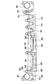
本発明に係る鍍金装置は、図1に示すように、少なくとも金属イオンが含有された鍍金浴307と、該鍍金浴307を保持する鍍金槽306と、長尺状の導電性基板303を搬送して該鍍金浴307に浸漬させる搬送装置301,302,309と、前記導電性基板303の一面側(図1の場合は下面側)に対向するように前記鍍金浴中に配置された対向電極305と、前記導電性基板303と前記対向電極305との間に電圧を印加して前記導電性基板303の一面側に鍍金を施す電圧印加手段308と、前記導電性基板303と前記電圧印加手段308との電気的接続を行うための給電部材310と、を備えている。この長尺状の導電性基板303は、鍍金工程以降に短く切断される場合が多いが、この明細書においては、その切断前のものを“長尺基板”として切断後のものと区別することとする。搬送装置は、送り出しローラー301、巻取りローラー302、搬送ローラー309に分類される。また、本例では、給電部材310が搬送ローラーを兼ねているが、給電部材を搬送ローラーとは別に設けても良いし、給電部材310と電圧印加手段308はアースを介して接続されていても良い。
【0032】
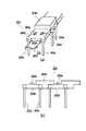
ところで、本発明に係る鍍金装置は、符号304で示すように、長尺基板303の他面側(図1の場合は上面側)に配置された膜析出抑制手段を備えている。この膜析出抑制手段304は、図2(a) に詳示するように、前記長尺基板303の他面側(符号303a参照)における短手方向端縁(符号303b参照)に少なくとも一部が近接するように前記鍍金槽306に固定配置されており、しかも、少なくとも該短手方向端縁に近接する部分が導電性を有するように構成されている。そして、該膜析出抑制手段304における前記導電性を有する部分(以下、“導電部分”とする)と前記長尺基板303とがほぼ同電位に保持されることに基づき、前記長尺基板の他面側303aへの膜析出が抑制されるようになっている。
【0033】
なお、前記長尺基板の他面側303aへの膜析出を抑制するには、図2(a) に示すように、膜析出抑制手段304を(前記短手方向端縁303bに近接する部分にのみ配置するのではなくて)前記長尺基板の他面側303aの全面に沿うように配置する方が良い。その場合、前記短手方向端縁303bに近接する部分だけが導電性を有するようにしても、前記長尺基板の他面側303aに沿う部分の全体が導電性を有するようにしても良い。本発明の装置を簡単に製造するという観点からは、膜析出抑制手段304のうち前記長尺基板の他面側303bの全面に沿うように配置される部分(後述する304b,304d)全体を導電性部材(例えば、ステンレスなどの金属部材)とすることが好ましい。また、膜析出抑制手段を、前記長尺基板の他面側303aに沿うように水平に配置するのではなく、両方の端縁303b,303bから上方に延設されるような垂直に(壁状に)配置するようにしても良い。そのような垂直壁を導電部材で構成した場合には、長尺基板の他面側303aへの膜析出を抑制することができる。
【0034】
ところで、上述のように該膜析出抑制手段304における前記導電部分と前記長尺基板303とをほぼ同電位にするためには、該導電部分と接触するように前記搬送装置301,302,309が該長尺基板303を搬送すれば良い。この場合、前記膜析出抑制手段304に磁石(図2(a) (b) の符号304a参照)を配置し、前記長尺基板303が、前記磁石304aに引き寄せられて前記膜析出抑制手段304に接触されるようにすると良い。なお、図2(a) (b) では、磁石304aを上側に載置しているが、埋め込んでも、膜析出抑制手段自体を磁石製としても良い。また、該膜析出抑制手段304における前記導電部分と前記長尺基板303とが接触されていなくても、共に、電源に接続されていても、アースされていても良い。
【0035】
このように、前記導電部分と前記長尺基板303とをほぼ同電位にする意義は、前記導電部分に裏面膜付着を防止させるための電気的なシールドの役割を持たせる点にある。従って、完全に同電位ではなかったとしてもある程度の効果を得ることができる。そして、容易に「ほぼ同電位」を実現する手法として、前記導電部分と前記長尺基板303とを接触させるのが好ましい。加えて、前記膜析出抑制手段を前記導電性基板の短手方向の端縁の外側に延在させる(換言すれば、前記膜析出手段の基板短手方向の幅を基板短手方向の幅より大きくしてはみ出させる)構成とすれば、導電性基板の短手方向端縁への電解集中を防止し、該端縁での異常な膜成長を防ぐという効果を得ることもできる。かかる延在幅としては片側あたり5mm〜50mm程度とすることが好ましい。
【0036】
また、前記膜析出抑制手段304が、前記導電部分を支持するための脚部304cを有するようにすると良い。また、前記短手方向端縁303b(正確には、前記長尺基板の他面側における短手方向端縁303b)に近接するように配置される第1部材304bを有し、該第1部材304bが前記脚部304cにて支持されるようにし、該第1部材304bは、前記長尺基板303の長手方向に沿うように、かつ、互いに離間した状態に複数固定配置すると良い。この場合、前記第1部材304bと前記第1部材304bとの間隙を閉塞するように第2部材304dを配置すると良い。そして、第1部材304bや第2部材304dは、少なくとも前記長尺基板の短手方向端縁303bに近接する部分が導電性を有する、ようにすると良い。また、第2部材304dは長尺基板303に接するように配置すると良い。膜析出抑制手段を長尺状部材にて形成するのではなくて、上述のように複数の第1部材304bに分割した場合には、各第1部材304bの平滑性を良好にして長尺基板303との接触を容易に実現できる。また、このように分割されているために第1部材304bの交換等も容易にでき、膜析出抑制手段のメンテナンスも簡単となる。第1部材304bに脚部304cを嵌めんで固定されるように設計しておけば、第1部材の取外しもさらに容易になる。さらに、第2部材304dが第1部部材304bに嵌合するように構成してすることが好ましい。このようにすることによって、第2部材304dを容易に取外すことができるので、対向電極305の交換等のメンテナンスを行う必要が生じた場合でも、第1部材304bと第1部材304bとの間隙を利用して作業を行うことができるので、対向電極305等のメンテナンスも容易になる。本例の第1部材304bとしては厚さ0.5〜10mm、大きさB5乃至A2の導電性を有する平板とすることが、ハンドリングの点から好ましい。また、第2部材304dとしては、厚さ0.5〜10mm程度で長尺基板の短手方向に相当する方向の長さが第1部材と同等で、長尺基板の長手方向の長さが第1部材304bと同等以下であり導電性を有する平板上に、第1部材304b相互の間隙に相当する大きさ及び厚さを有する導電性を有する平板を溶接するなどして固定することによって凸部を形成したものが好ましい。第1部材304b、第2部材304dの大きさは、長尺基板の短手方向幅との兼ね合いで決定することができる。なお、第1部材304bの位置決めは脚部304cにて行えば良く、第2部材304dの位置決めは第1部材304bにて行えば良い。また、脚部304cの代わりに、鍍金槽306の側壁面や鍍金槽の外部に固定された支持部材を用いることも可能である。
【0037】
ところで、上述した膜析出抑制手段304は、前記長尺基板303の短手方向の端縁の外側に延在するように配置すると良い。つまり、膜析出抑制手段304の短手方向寸法(長尺基板303の搬送方向と直交する方向の寸法)が長尺基板303の短手方向寸法よりも大きくなるようにしておくと良い。 本発明に係る鍍金装置は、少なくとも金属イオンが含有された鍍金浴307を保持する鍍金槽306と、長尺基板303を搬送して該鍍金浴307に浸漬させる搬送装置301,302と、前記長尺基板303の一面側に対向するように前記鍍金浴中に配置された対向電極305と、前記長尺基板303と前記対向電極305との間に電圧を印加して前記長尺基板303の一面側に鍍金を施す電圧印加手段308と、を備えており、前記長尺基板の他面側303aに少なくとも一部が接触するように前記鍍金槽306に固定配置されると共に、少なくとも前記長尺基板303の他面側303aに接触する部分が導電性を有する部材304、を有する。そして、前記部材304が前記長尺基板303との接触を維持するための磁石304aを有する。前記部材304が、前記長尺基板303の長手方向に複数の第1部材303bと複数の第2部材303dとを有する。前記第1部材304bが互いに間隙を介して複数配置され、該複数の第1部材304bが支持部材(脚部)によって固定されており、前記第2部材304dが2つの互いに隣接する第1部材304bの上面にわたって配置されている。前記第1部材304bの前記長尺基板側の表面がほぼ平面であり、前記第2部材304dが、図2(a) (b) に詳示するように、前記間隙を埋める凸部を有しており、該凸部の前記長尺基板側の表面と前記第1部材304bの前記長尺基板側の表面とがほぼ同一平面上に配置される。
【0038】
なお、本発明においては、給電手段310と長尺基板303とが電気的に導通されるように構成すると共に、対向電極305と給電手段310との間に電圧印加手段308を介装して電圧を印加するようにすると良い。
【0039】
一方、本発明に係る鍍金方法は、鍍金槽306に保持された鍍金浴307に長尺基板303を通過させるように搬送し、該鍍金浴中で該長尺基板303の一面側に電気鍍金を施すものであって、膜析出抑制手段304を鍍金槽306に固定配置して、前記長尺基板の他面側303aにおける短手方向端縁303bに近接するようにし、かつ、該膜析出抑制手段304を前記長尺基板303とほぼ同電位に保持することにより、前記長尺基板の他面側303aへの膜析出を抑制するようにしたものである。
【0040】
この場合、前記膜析出抑制手段304を前記長尺基板303に接触させることにより、それらをほぼ同電位にすると良い。また、前記膜析出抑制手段304は、磁力により前記長尺基板303に接触させると良い。さらに、前述したような特徴を有する装置を用いることができる。
【0041】
本実施の形態によれば、長尺基板303の他面側への膜析出を抑制できる。したがって、鍍金工程後に長尺基板303を真空装置内に入れなければならないような場合であっても、脱ガスに伴う種々の問題を低減できる。また、真空装置内において膜が剥がれ落ちる問題も低減できる。さらに、剥がれ落ちた膜が異物として混入したりすることも抑制できる。また、ロール・ツー・ロール形式の搬送方法を用いる場合においても、膜析出が原因となって摩擦係数のばらつきから巻きずれや、搬送不具合が発生するおそれも低減できる。さらに、鍍金後の基板に半田溶接や接着被覆作業を行う場合であっても、接合強度を十分に確保できる。また、裏面の外観不良を防止することもできる。
【0042】
(酸化亜鉛層の鍍金装置、及び鍍金方法)
上述した鍍金装置及び鍍金方法の一例として、酸化亜鉛層を鍍金する装置及び方法について説明する。
【0043】
図中の符号306は酸化亜鉛層鍍金槽を示すが、この酸化亜鉛層鍍金槽は2槽配置している。そして、符号311はシャワー槽を示し、符号312はリンス槽を示し、符号313は乾燥用のエアーナイフを示し、符号314は乾燥用ヒーターを示す。搬送装置は、送り出しローラー301、巻取りローラー302、搬送ローラー309及び不図示のローラー駆動手段にて構成し、送り出しローラー301から送り出された長尺基板303が鍍金浴307に浸漬された後、巻取りローラー302に巻き取られるようにすれば良い。
【0044】
ところで、該装置にて酸化亜鉛層103を形成するに当たり、長尺基板303の表面にはスパッタ法等によって予め酸化亜鉛層を形成しておくと良い(特開平10−140373号公報参照)。このようにすることにより、電析される酸化亜鉛層と長尺基板との密着性を高めることができ、基板材料の溶出を防止することができる。
【0045】
また、酸化亜鉛層鍍金浴307には、少なくとも亜鉛イオンが含有された鍍金浴を用いる。亜鉛イオン濃度は、好ましくは0.002mol/l〜3.0mol/l、より好ましくは0.01mol/l〜1.5mol/l、さらに好ましくは0.05mol/l〜0.7mol/lである。この鍍金浴307には、硝酸イオン、亜鉛イオン及びサッカロースまたはデキストリンを含有させた方が良い。その場合の硝酸イオン濃度は、好ましくは0.004mol/l〜6.0mol/l、より好ましくは0.01mol/l〜1.5mol/l、さらに好ましくは0.1mol/l〜1.4mol/lである。また、サッカロースの濃度は、好ましくは1g/l〜500g/l、より好ましくは3g/l〜100g/l、デキストリンの濃度は、好ましくは0.01g/l〜10g/l、より好ましくは0.025g/l〜1g/lである。このようにすることで、光閉じ込め層として好適なテクスチャー構造の酸化亜鉛層を効率よく形成できる。
【0046】
また、この鍍金浴307には、SP2混成軌道を存する隣接する炭素のそれぞれにカルボキシル基が結合した化合物を0.5μmol/l〜500μmol/l含有させることが好ましい。このようにすることで、酸化亜鉛層表面の凹凸を大きくすることができる。かかる化合物の具体例としては、フタル酸、マレイン酸、フタル酸水素カリウム等のフタル酸誘導体が挙げられる(特開2002−167695号公報参照)。
【0047】
酸化亜鉛層鍍金浴307の電導度としては、例えば10mS/cm以上100mS/cm以下が挙げられるが、反応性を考慮すると50mS/cm以上であることがより好ましい。また電導度が高くなると鍍金浴の反応性が高くなるため端部での裏面回り込みを制御することが難しくなる。更に、前述のように表面の堆積膜上にミクロンオーダーを超えるような針状や球状もしくは樹枝状の形状をした異常成長が発生しやすくなる。そのため電導度の上限は100mS/cm以下が望ましい。
【0048】
また、対向電極305には亜鉛板を用い、電圧印加手段308には定電流電源を用いると良い。
【0049】
ここで、長尺基板303と対向電極305との間の電流密度(絶対値)としては、0.1mA/cm2以上100mA/cm2が挙げられるが、電導度と同様に反応性や表面に形成する膜の形状を考慮すると1mA/cm2以上30mA/cm2以下であることがより好ましく、3mA/cm2以上15mA/cm2以下であることがさらに好ましい。なお、対向電極305を(長尺物で1枚とするより)図示のように複数に分割した方が、ハンドリングやメンテナンス等の観点からは好ましい。
【0050】
ところで、この酸化亜鉛層鍍金槽306にヒータや温度計(不図示)を配置して鍍金浴の温度を50℃以上100℃以下に保持し、異常成長の少ない均一な酸化亜鉛層を効率よく形成できるようにすると良い。また、循環ポンプ(不図示)や磁気攪拌子等を用いて鍍金浴を循環するようにしても良い。
【0051】
以上説明したような鍍金装置や鍍金方法を用いて図3に示すような光起電力素子を作製すると良い。以下、この光起電力素子について説明する。
【0052】
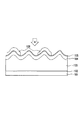
ここで、図3は、本発明に係る製造装置にて製造できる光起電力素子の一例を示す断面模式図である。図中101は支持体、102は金属層(反射層)、103は酸化亜鉛層、104は半導体層、105は透明導電層、106は集電電極である。このような光起電力素子を製造するには、支持体101を長尺状とし、その表面に金属層102を形成し、次に、酸化亜鉛層103を図1に示す鍍金装置によって形成し、その後切断するが、切断前の長尺状の支持体101と金属層102の一体物が上述した長尺基板303に相当することとなる。なお、図3に示す側から光が入射される光起電力素子では、図示のように、支持体101、金属層102、酸化亜鉛層103、半導体層104、透明導電層105、集電電極106の順に積層すれば良いが、支持体下側から光が入射される光起電力素子では、支持体以外の積層順を逆にして、支持体101、集電電極106、透明導電層105、半導体層104、酸化亜鉛層103、金属層102の順で積層させれば良い。
【0053】
次に、上記光起電力素子の構成要素及びその製造方法について説明する。
【0054】
(支持体)
支持体101としては、ステンレスなどからなる金属基板、樹脂基板、ガラス基板、セラミック基板等が用いられる。その表面には微細な凹凸を有してもよい。なお、光の入射方向を図3に矢印で示す方向ではなくて反対方向とする場合、支持体101には透明基板を用いる必要がある。
【0055】
(金属層)
金属層102には、電極としての役割と、支持体101にまで到達した光を反射して半導体層104で再利用させる反射層としての役割がある。この金属層102は、金、銀、銅、アルミニウムもしくはそれぞれの化合物などで形成すると良く、その成膜方法には、蒸着、スパッタ、電解析出法、印刷法等の方法を用いると良い。
【0056】
また、金属層102の表面に凹凸を設けることにより、反射光の半導体層104内での光路長を延ばし、短絡電流を増大させることができる。
【0057】
尚、支持体101が導電性を有する場合には金属層102は形成しなくてもよい。その場合、切断前の長尺状の支持体101が上述した長尺基板303に相当する。もっとも、表面凹凸の形状を制御するという観点からは、支持体が導電性を有する場合であっても、金属層102を設けたほうが良い。
【0058】
(酸化亜鉛層)
酸化亜鉛層(透明導電層)103には、入射光及び反射光の乱反射を増大させ、半導体層104内での光路長をのばす役割がある。かかる効果を発現させるためには、六方晶系多結晶の酸化亜鉛層が好ましい。また、酸化亜鉛層103は、金属層102の原子やイオンが半導体層104へ拡散あるいはマイグレーションを起こし、光起電力素子がシャントすることを防止する役割を有する。さらに、酸化亜鉛層103に適度な抵抗を持たせることにより、半導体層104のピンホール等の欠陥によるショートを防止することができる。酸化亜鉛層103は金属層102と同様その表面に凹凸を有していることが望ましい。
【0059】
(半導体層)
半導体層104の材料としては、アモルファスあるいは微結晶のSi、C、Ge、またはこれらの合金が好適に用いられる。半導体層104には同時に、水素及び/またはハロゲン原子が含有されることが望ましい。その望ましい含有率は0.1〜40atom%である。半導体104は更に酸素、窒素などの不純物を含有してよい。これらの不純物量は5×1019mol/cm3以下が望ましい。さらに半導体層104をp型半導体とするにはIII族元素、n型半導体とするにはV族元素を含有させることが望ましい。
【0060】
半導体層104がpin接合を複数有するスタックセルの場合、光入射側に近いpin接合のi型半導体層はバンドギャップが広く、遠いpin接合になるに従いバンドギャップが狭くなるのが望ましい。また、i型層の内部ではその膜厚の中央よりもp型層よりにバンドギャップの極小値があるのが望ましい。好適な例として、光入射側から順に、アモルファスi型層を有するpin接合と微結晶i型層を有するpin接合とを積層したダブルセルや、光入射側から順に、アモルファスi型層を有するpin接合、微結晶i型層を有するpin接合、微結晶i型層を有するpin接合を積層したトリプルセルが挙げられる。
【0061】
光入射側のドープ層(p型層、n型層)は光吸収の少ない結晶性の半導体か、またはバンドキャップの広い半導体が適している。
【0062】
半導体層104を形成する方法としては、マイクロ波(MW)プラズマCVD法、VHFプラズマCVD法またはRFプラズマCVD法が適している。
【0063】
(透明導電層)
透明導電層105はその膜厚を適当に設定することにより反射防止膜の役割を兼ねることができる。この透明導電層105はITO(インジウム錫酸化物)、ZnO、In2O3等の材料を、蒸着、CVD、スプレー、スピンオン、浸漬などの方法を用いて成膜することにより形成される。これらの化合物に導電率を変化させる物質を含有させてもよい。
【0064】
(集電電極)
集電電極106は集電効率を向上させるために設けられる。その形成方法として、マスクを用いたスパッタによる金属の集電パターンの形成方法や、半田ペーストや銀ペースト等の導電性ペーストを印刷する方法、金属線を導電性ペーストで固着する方法などがある。
【0065】
なお、必要に応じて光起電力素子の両面に保護層を形成することがある。同時に鋼板等の補強材を併用してもよい。
【0066】
【実施例】
以下、実施例により本発明を詳しく説明するが、本発明はこれらの実施例に限定されるものではない。
【0067】
(実施例1)
本実施例では、図3に示す構造の光起電力素子を作製した。すなわち、支持体101の表面に、金属層102や酸化亜鉛層103や半導体層104や透明導電層105や集電電極106を順に形成した。
【0068】
上述のような光起電力素子を作製するに当たっては、厚さ0.15mm、幅355mm、長さ500mのステンレス430−2D板(上述した長尺基板に相当)303を用意し、その表面にはスパッタ法によって800nm厚の銀層(上述の金属層102に相当)を形成し、さらにその表面にはスパッタ法によって200nm厚の酸化亜鉛層を形成した。
【0069】
その後、図1に示す鍍金装置を用い、既に形成してある酸化亜鉛層の表面に新たな酸化亜鉛層(図3に符号103で示す酸化亜鉛層の大部分)を2.6μmの厚さで析出させた。
【0070】
本実施例にて用いた鍍金装置は、2つの酸化亜鉛層鍍金槽306,306を配置して構成し、その下流側(正確には、長尺基板の搬送方向下流側)にはシャワー槽311、2つのリンス槽312、エアーナイフ313、ヒーター314を配置した。そして、それらの槽306,311,312の上流及び下流側には送り出しローラー301及び巻取りローラー302をそれぞれ配置するとともに複数の搬送ローラー309を配置し、ロール・ツー・ロール方式によって長尺基板303を搬送するようにした。
【0071】
一方、鍍金浴307は、硝酸亜鉛0.2mol/l、デキストリン0.1g/l、フタル酸水素カリウム10mg/lの水溶液とし、浴温は80℃とした。
【0072】
また、各槽306には23枚の対向電極305をそれぞれ配置したが、1枚の対向電極305には、幅(長尺基板搬送方向と直交する方向の寸法)が400mmで、長さ(長尺基板搬送方向の寸法)が150mmの4−N(99.99%)の亜鉛板を用いた。
【0073】
さらに、給電部材310と対向電極305の間には定電流電源308を介装して対向電極側が正極性となるように電圧を印加し、6.7mA/cm2の密度(1枚の対向電極当りでは、6.7mA/cm2×40cm×15cm≒4A)の電流を流した。
【0074】
一方、膜析出抑制手段304は、図2に示すように、磁石304aを2つ有する複数の平板状部材(第1部材)304bと、各平板状部材304bの隅部から垂下された脚部304cと、平板状部材304bの間隙に配置された閉塞部材(第2部材)304dと、によって構成し、平板状部材304b及び閉塞部材304dが長尺基板303の上面に接触するようにした。第1部材304bとしては厚さ1mm、幅375mm、長さ500mmのステンレス製平板を用いた。また、第2部材304dとしては、厚さ1mm、幅375mm、長さ250mmのステンレス製平板に、厚さ1mm、幅375mm、長さ50mmのステンレス製平板を溶接して凸部を形成したものを用いた。そして、各槽306あたり第1部材304bを26枚、第2部材304dを25枚配置し、前記凸部が隣りあう第1部材の間隙を埋めるようにするとともに、第1部材及び第2部材が長尺基板基板幅方向端縁の外側に10mmずつはみ出すようにした。
【0075】
このような装置を用いて鍍金処理を施したところ、長尺基板下面側には酸化亜鉛層がほぼ均一な厚さに形成されたものの、長尺基板上面側には酸化亜鉛はほとんど析出していなかった。なお、不可避的に発生する長尺基板の搬送ムラによって、基板短手方向端縁303bの一部にごく少量の裏面膜付着が観察された。これにより、真空装置内における脱ガスや膜剥がれの問題を回避でき、摩擦係数のばらつきに伴う搬送不具合という問題も回避でき、後工程で半田溶接等を行う場合であっても、接合強度を十分に確保できた。
【0076】
その後、酸化亜鉛層103の表面にはpin接合を3つ積層した構造(光入射側から順に、アモルファスi型層を有するpin接合、微結晶i型層を有するpin接合、微結晶i型層を有するpin接合を積層した構造)の半導体層104をロール対応のCVD装置にて形成し、さらにロール対応スパッタ装置によりITOを透明導電層105として堆積せしめた。しかるのち、銀ペーストで集電電極106を作成し、光起電力素子を得た。
【0077】
(実施例2)
本実施例では、第2部材304dとして、厚さ1mm、幅375mm、長さ250mmのステンレス製平板を用い、隣合う第1部材に跨るように配置した。即ち、第1部材相互の間隙において長尺基板と第2部材との間に厚さ1mm程度の隙間が生じるようにした。その他の構成や製造方法は実施例1と同様とした。
【0078】
本実施例によれば、長尺基板303の上面側の短手方向端縁303bに多少の酸化亜鉛が析出したものの、膜析出抑制手段304を用いない場合(この場合、裏面全体にわたって低密度で脆い膜が大量に付着する)に比べて、その析出量は飛躍的に低減されていた。その結果、上記実施例1とほぼ同様の効果が得られた。
【0079】
【発明の効果】
以上説明したように、本発明によれば、導電性基板の他面側への膜析出を抑制できる。したがって、鍍金工程後に該導電性基板を真空装置内に入れなければならないような場合であっても、脱ガスに伴う種々の問題を低減できる。また、真空装置内において膜が剥がれ落ちる問題も低減できる。さらに、剥がれ落ちた膜が異物として混入したりすることも抑制できる。また、外観不良も低減できる。また、ロール・ツー・ロール形式の搬送方法を用いる場合においても、膜析出が原因となって摩擦係数のばらつきから巻きずれや、搬送不具合が発生するおそれも低減できる。さらに、鍍金後の基板に半田溶接や接着被覆作業を行う場合であっても、接合強度を十分に確保できる。
【図面の簡単な説明】
【図1】本発明に係る鍍金装置を示す模式図である。
【図2】 (a) は膜析出抑制手段の外観を示す斜視図であり、(b) はその側面図である。
【図3】本発明に係る製造装置にて製造できる光起電力素子の一例を示す断面模式図である。
【符号の説明】
101 支持体
102 金属層
103 酸化亜鉛層
104 半導体層
105 透明導電層
106 集電電極
301 送り出しローラー(搬送装置)
302 巻取りローラー(搬送装置)
303 長尺基板(導電性基板)
304 膜析出抑制手段
304b 平板状部材(第1部材)
304d 閉塞部材(第2部材)
305 亜鉛板(対向電極)
306 酸化亜鉛層鍍金槽
307 酸化亜鉛層鍍金浴
308 定電流電源(電圧印加手段)
309 搬送ローラー(搬送装置)
310 給電部材[0001]
BACKGROUND OF THE INVENTION
The present invention relates to a plating apparatus and a plating method for plating a long conductive substrate.
[0002]
[Prior art]
A plating apparatus and a plating method for continuously plating a long conductive substrate are used in various technical fields. For example, a photovoltaic element such as a solar cell is formed by laminating a support, a reflective layer, a transparent layer (for example, a zinc oxide layer), a semiconductor layer, and a transparent conductive layer. A plating apparatus or a plating method for a scale substrate is used.
[0003]
Hereinafter, the configuration of the photovoltaic element, the manufacturing method thereof, and the like will be described.
[0004]
As the semiconductor layer, hydrogenated amorphous silicon, hydrogenated amorphous silicon germanium, hydrogenated amorphous silicon carbide, microcrystalline silicon, polycrystalline silicon, or the like is used.
[0005]
The reflection layer plays a role of improving the absorption efficiency of long-wavelength light, and desirably exhibits effective reflection characteristics at a wavelength near the band edge of the semiconductor material where the absorption becomes small, that is, from 800 nm to 1200 nm. A metal layer made of a material such as gold, silver, copper, or aluminum sufficiently satisfies this condition.
[0006]
The transparent layer (for example, zinc oxide layer) is disposed between the reflective layer and the semiconductor layer to confine light, and effectively improves the short-circuit current density Jsc by effectively using the reflective layer. It is. Further, in order to prevent deterioration of characteristics due to the shunt path, a layer made of a light-transmitting material showing conductivity, that is, a transparent conductive layer is provided between the reflective layer and the semiconductor layer. Most commonly, these layers are deposited by methods such as vacuum evaporation and sputtering, with a short circuit current density Jsc of 1 mA / cm. 2 These improvements are shown.
[0007]
For example, “Optical confinement effect in a-SiGe solar cell on 29p-MF-22 stainless steel substrate” (Autumn 1990), p747, or “P-IA-15a-SiC” / A-Si / a-SiGe Multi-Bandgap Stacked Solar Cells With Bandgap Profiling ", Sannomiya et al. , Technical Digest of the International PVSEC-5, Kyoto, Japan, p381, 1990, discusses the reflectance and texture structure of a reflective layer composed of silver atoms. In these examples, an effective unevenness is formed by using a two-layer deposition of silver whose substrate temperature is changed in the reflection layer, and a short circuit current due to the light confinement effect is formed by a combination with the zinc oxide layer provided thereon. The increase is said to have been achieved.
[0008]
The transparent layer used as the optical confinement layer is deposited by resistance heating or electron beam vacuum deposition, sputtering, ion plating, CVD, etc., but the vacuum device is expensive and the target The high production cost of materials, etc., and the low utilization efficiency of materials, etc., make solar cells industrially applicable as the manufacturing cost of photovoltaic devices using these technologies is extremely high. It is a big obstacle.
[0009]
As one method for solving such problems, there is a technique for producing zinc oxide by a liquid layer deposition method (“Preparation of ZnO Film by Aqueous Solution Electrolysis” (Autumn 1995), Proceedings of the 65th JSAP Scientific Presentation). It has been reported.
[0010]
Japanese Patent Application Laid-Open No. 10-195893 proposes a method for forming a zinc oxide layer by electrolytic deposition (synonymous with electroplating; hereinafter abbreviated as electrodeposition). In this publication, a zinc oxide layer is formed on a conductive substrate by immersing a conductive substrate or electrode in an aqueous solution containing nitrate ions, zinc ions, and carbohydrates, and applying a voltage between them. A method is disclosed.
[0011]
Furthermore, Japanese Patent Laid-Open No. 10-14373 proposes a method for forming a zinc oxide layer by electrodeposition, which is uniform and has excellent substrate adhesion. Specifically, a step of forming a first zinc oxide layer on the substrate by sputtering, and the substrate is immersed in an aqueous solution containing at least nitrate ions, zinc ions, and carbohydrates, and immersed in the solution There is disclosed a method for producing a zinc oxide layer including a step of forming a second zinc oxide layer on the first zinc oxide layer by energizing between the formed electrodes.
[0012]
According to these methods, since an expensive vacuum apparatus and target are unnecessary, the manufacturing cost of zinc oxide can be drastically reduced. Further, since it can be deposited on a large area substrate, it is promising for a large area photovoltaic element such as a solar cell.
[0013]
[Problems to be solved by the invention]
However, this electrochemical method for depositing zinc oxide has further problems to be solved.
[0014]
That is, when a zinc oxide layer is formed by the electrodeposition method, if a conductive substrate is used, the zinc oxide layer is applied not only to the film formation surface (= front surface) but also to the non-film formation surface (= back surface). Will be deposited. The zinc oxide layer deposited on the back surface of the substrate (hereinafter referred to as “back surface film”) is a zinc oxide layer deposited on the surface of the substrate depending on the deposition conditions (mainly due to the application of an electric field, etc.). It may become a foreign film. Specifically, a fragile film may be formed even at a low density with different surface irregularities and mechanical strength. When such a back surface film exists to some extent, the following problems occur when forming a semiconductor element such as a photovoltaic element (solar cell), for example.
[0015]
(1) When a substrate on which a zinc oxide layer is formed by electrolytic deposition is supplied to the manufacturing process of the photovoltaic device, there is a risk of deteriorating photoelectric conversion characteristics due to degassing in a vacuum apparatus. In particular, since the backside film has a small density and easily has a large surface area, there is a high risk of bringing oxygen, nitrogen, water, and other adsorbed gases into the vacuum apparatus.
[0016]
(2) When the substrate is transported in the vacuum apparatus, the back surface film may be peeled off and become dust, contaminating the inside of the vacuum apparatus and being mixed into the semiconductor film or the like to deteriorate the characteristics.
[0017]
(3) When the roll-to-roll method is used, the back film is also simultaneously wound in the winding process, and there is a possibility that it will be peeled off during winding and mixed between the substrates. In this case, there is a risk that foreign matter comes into contact with the zinc oxide layer deposited on the surface and is damaged.
[0018]
(4) There is a possibility that winding deviation or conveyance failure may occur due to variations in the friction coefficient due to the presence of the back film.
[0019]
(5) When solder welding or adhesive coating on the back surface is performed as post-processing after the zinc oxide layer is formed, film adhesion on the back surface of the substrate can cause deterioration of workability such as poor welding or poor adhesion.
[0020]
Also in other technical fields, when it is desired to apply plating only to one surface (front surface) of a long conductive substrate, the presence of film adhesion on the back surface may adversely affect post-processing, impair aesthetics, etc. A problem occurs. Therefore, there is a demand for a method of preventing the back surface film from being attached as much as possible, or removing the attached back surface film.
[0021]
Therefore, as one method for removing the back film, Japanese Patent Application Laid-Open No. 11-286799 discloses a method of etching the zinc oxide layer deposited on the back surface by electrolysis using a back film adhesion preventing electrode. By this method, the back film can be greatly reduced. However, it is difficult to remove only the zinc oxide layer deposited on the back surface without adversely affecting the zinc oxide layer deposited on the surface. In addition, when a metal film reactive with an oxidizing liquid such as silver is used between the substrate and zinc oxide, an electrochemical reaction reaches the metal film by an electric field for etching. Problems such as discoloration and dissolution may occur in the metal film.
[0022]
Japanese Patent Laid-Open No. 10-60686 discloses a non-plated surface by disposing an insulator functioning as a shielding member between the edge portion of the strip and the anode when continuously plating one surface of the metal strip. A technique for preventing the adhesion of plating is described. A similar shielding technique is also described in Japanese Patent Laid-Open No. 2002-155395. However, in these techniques, there is a problem that it is extremely difficult to optimally design an apparatus for performing uniform plating on a plating surface and at the same time effectively preventing plating adhesion to a non-plating surface. Furthermore, since the optimum design may vary depending on the plating conditions, it can be said that it is almost impossible to design an apparatus that can flexibly cope with changes in the plating conditions.
[0023]
Japanese Patent Application Laid-Open No. 10-259596 proposes a technique in which a zinc oxide layer is not deposited on the back surface of a substrate when a zinc oxide layer is formed by electrodeposition. Specifically, an unnecessary zinc oxide layer is formed on the back surface of the substrate by providing a rotating belt for transporting the substrate while covering one surface of a long substrate immersed in an aqueous solution containing nitrate ions and zinc ions. Techniques that do not deposit are disclosed.
[0024]
According to this method, it is possible to effectively suppress the deposition of the back surface film, but since the configuration for transporting the member that covers the back surface of the substrate is essential, the configuration of the apparatus becomes complicated and at the same time the cost increases. Connected.
[0025]
An object of the present invention is to provide a plating apparatus and a plating method that suppress unnecessary deposition of a film on a conductive substrate at a low cost.
[0026]
[Means for Solving the Problems]
The present invention has been made in view of the above circumstances, and includes a plating tank that holds a plating bath containing at least metal ions, and a transport device that transports a long conductive substrate and immerses it in the plating bath. And a counter electrode disposed in the plating bath so as to face the one surface side of the conductive substrate, and a voltage is applied between the conductive substrate and the counter electrode so as to face the one surface side of the conductive substrate. And a voltage applying means for applying plating to the plating tank, and is fixedly disposed in the plating tank so as to be at least partially close to an edge in a short direction on the other surface side of the conductive substrate, A portion adjacent to the edge in the short direction has conductive film deposition suppressing means, and the conductive portion and the conductive substrate in the film deposition suppressing means are held at substantially the same potential. Based on said conductive substrate Film deposition is suppressed to the other side In addition, the film deposition suppressing means includes a first member disposed so as to be close to a short-side edge on the other surface side of the conductive substrate, and the first member is a longitudinal length of the conductive substrate. A plurality of fixed and arranged along the direction and separated from each other, It is characterized by that.
[0027]
The present invention also provides a plating tank for holding a plating bath containing at least metal ions, a transporting device for transporting a long conductive substrate and immersing it in the plating bath, and one side of the conductive substrate. A counter electrode disposed in the plating bath so as to oppose the electrode, and voltage applying means for applying a voltage between the conductive substrate and the counter electrode to apply plating to one surface side of the conductive substrate, In the plating apparatus comprising: a conductive tank, the plating tank is fixedly disposed in the plating tank so that at least a part thereof contacts the other surface side of the conductive substrate, and at least a portion that contacts the other surface side of the conductive substrate is conductive. Have A member, and the member has a magnet for maintaining contact with the conductive substrate It is characterized by that.
[0028]
Furthermore, the present invention conveys a long conductive substrate while passing it through a plating bath held in a plating tank, and on one side of the conductive substrate in the plating bath. Electrical In the plating method to apply the plating,
The film deposition suppressing means having the same potential as that of the conductive substrate is fixedly arranged in the plating tank so as to be close to the edge in the short direction on the other surface side of the conductive substrate. Suppresses film deposition on the other side of a conductive substrate In addition, by transporting the conductive substrate while bringing the film deposition inhibiting means into contact with the conductive substrate by magnetic force, they are made substantially the same potential. It is characterized by that.
[0029]
In the present invention, the term “fixed to the plating tank” refers not only to the case where it is directly fixed to the plating tank, but also the position relative to the plating tank changes by being fixed to a member other than the plating layer or the ground. Including the case of not.
[0030]
DETAILED DESCRIPTION OF THE INVENTION
Embodiments of the present invention will be described below with reference to the drawings.
[0031]
As shown in FIG. 1, the plating apparatus according to the present invention conveys a
[0032]
By the way, the plating apparatus according to the present invention is provided with a film deposition suppressing means arranged on the other surface side (upper surface side in the case of FIG. 1) of the
[0033]
In order to suppress the film deposition on the
[0034]
Incidentally, as described above, in order to make the conductive portion in the film deposition suppressing means 304 and the
[0035]
Thus, the significance of setting the conductive portion and the
[0036]
The film deposition suppressing means 304 may have a
[0037]
By the way, the film deposition suppressing means 304 described above is preferably arranged so as to extend outside the edge of the
[0038]
In the present invention, the power supply means 310 and the
[0039]
On the other hand, the plating method according to the present invention is such that the
[0040]
In this case, it is preferable that the film deposition suppressing means 304 is brought into contact with the
[0041]
According to the present embodiment, film deposition on the other surface side of the
[0042]
(Zinc oxide layer plating apparatus and plating method)
As an example of the plating apparatus and plating method described above, an apparatus and method for plating a zinc oxide layer will be described.
[0043]
[0044]
By the way, when forming the
[0045]
The zinc oxide
[0046]
The
[0047]
The conductivity of the zinc oxide
[0048]
Further, a zinc plate may be used for the
[0049]
Here, the current density (absolute value) between the
[0050]
By the way, a heater and a thermometer (not shown) are disposed in the zinc oxide
[0051]
A photovoltaic device as shown in FIG. 3 may be manufactured using the plating apparatus and the plating method described above. Hereinafter, this photovoltaic element will be described.
[0052]
Here, FIG. 3 is a schematic cross-sectional view showing an example of a photovoltaic element that can be manufactured by the manufacturing apparatus according to the present invention. In the figure, 101 is a support, 102 is a metal layer (reflection layer), 103 is a zinc oxide layer, 104 is a semiconductor layer, 105 is a transparent conductive layer, and 106 is a collecting electrode. In order to manufacture such a photovoltaic device, the
[0053]
Next, components of the photovoltaic element and a manufacturing method thereof will be described.
[0054]
(Support)
As the
[0055]
(Metal layer)
The
[0056]
Further, by providing unevenness on the surface of the
[0057]
Note that the
[0058]
(Zinc oxide layer)
The zinc oxide layer (transparent conductive layer) 103 has a role of increasing the irregular reflection of incident light and reflected light and extending the optical path length in the
[0059]
(Semiconductor layer)
As the material of the
[0060]
When the
[0061]
As the doped layer (p-type layer, n-type layer) on the light incident side, a crystalline semiconductor with little light absorption or a semiconductor with a wide band cap is suitable.
[0062]
As a method for forming the
[0063]
(Transparent conductive layer)
The transparent
[0064]
(Collector electrode)
The collecting
[0065]
In addition, a protective layer may be formed on both surfaces of the photovoltaic element as necessary. At the same time, a reinforcing material such as a steel plate may be used in combination.
[0066]
【Example】
EXAMPLES Hereinafter, although an Example demonstrates this invention in detail, this invention is not limited to these Examples.
[0067]
Example 1
In this example, a photovoltaic device having the structure shown in FIG. 3 was produced. That is, the
[0068]
In producing the photovoltaic element as described above, a stainless steel 430-2D plate (corresponding to the above-mentioned long substrate) 303 having a thickness of 0.15 mm, a width of 355 mm, and a length of 500 m is prepared, and the surface thereof is prepared. A 800 nm thick silver layer (corresponding to the
[0069]
Then, using the plating apparatus shown in FIG. 1, a new zinc oxide layer (most of the zinc oxide layer indicated by
[0070]
The plating apparatus used in this example is configured by arranging two zinc oxide
[0071]
On the other hand, the
[0072]
In addition, each of the
[0073]
Further, a voltage is applied between the
[0074]
On the other hand, as shown in FIG. 2, the film deposition suppression means 304 includes a plurality of flat plate members (first members) 304b having two
[0075]
When the plating process was performed using such an apparatus, the zinc oxide layer was formed with a substantially uniform thickness on the lower surface of the long substrate, but almost no zinc oxide was deposited on the upper surface of the long substrate. There wasn't. Note that a very small amount of the back surface film was observed on a part of the
[0076]
Thereafter, a structure in which three pin junctions are stacked on the surface of the zinc oxide layer 103 (in order from the light incident side, a pin junction having an amorphous i-type layer, a pin junction having a microcrystalline i-type layer, and a microcrystalline i-type layer are provided. The
[0077]
(Example 2)
In this example, a stainless steel flat plate having a thickness of 1 mm, a width of 375 mm, and a length of 250 mm was used as the
[0078]
According to the present embodiment, although some zinc oxide is deposited on the
[0079]
【The invention's effect】
As described above, according to the present invention, film deposition on the other surface side of the conductive substrate can be suppressed. Therefore, various problems associated with degassing can be reduced even when the conductive substrate must be placed in a vacuum apparatus after the plating process. In addition, the problem of film peeling off in the vacuum apparatus can be reduced. Further, it is possible to prevent the peeled film from being mixed as a foreign substance. Also, appearance defects can be reduced. In addition, even when a roll-to-roll type conveyance method is used, it is possible to reduce the risk of winding slip and conveyance failure due to variations in the friction coefficient due to film deposition. Furthermore, even when solder welding or adhesive coating work is performed on the substrate after plating, sufficient bonding strength can be ensured.
[Brief description of the drawings]
FIG. 1 is a schematic view showing a plating apparatus according to the present invention.
FIG. 2 (a) is a perspective view showing an appearance of a film deposition suppressing means, and FIG. 2 (b) is a side view thereof.
FIG. 3 is a schematic cross-sectional view showing an example of a photovoltaic element that can be manufactured by the manufacturing apparatus according to the present invention.
[Explanation of symbols]
101 Support
102 Metal layer
103 Zinc oxide layer
104 Semiconductor layer
105 Transparent conductive layer
106 Current collecting electrode
301 Feeding roller (conveying device)
302 Winding roller (conveying device)
303 Long substrate (conductive substrate)
304 Means for suppressing film deposition
304b Flat member (first member)
304d Closure member (second member)
305 Zinc plate (counter electrode)
306 Zinc oxide layer plating tank
307 Zinc oxide layer plating bath
308 Constant current power supply (voltage application means)
309 Conveying roller (conveying device)
310 Power supply member
Claims (7)
前記導電性基板の他面側における短手方向端縁に少なくとも一部が近接するように前記鍍金槽に固定配置されると共に、少なくとも該短手方向端縁に近接する部分が導電性を有する膜析出抑制手段、を有し、
該膜析出抑制手段における前記導電性を有する部分と前記導電性基板とがほぼ同電位に保持されることに基づき、前記導電性基板の他面側への膜析出が抑制されるとともに、
前記膜析出抑制手段は、前記導電性基板の他面側における短手方向端縁に近接するように配置される第1部材を有し、前記第1部材は、前記導電性基板の長手方向に沿うように、かつ、互いに離間した状態に複数固定配置された、
ことを特徴とする鍍金装置。A plating tank for holding a plating bath containing at least metal ions, a transporting device for transporting a long conductive substrate and immersing it in the plating bath, and the one facing the one side of the conductive substrate. In a plating apparatus comprising: a counter electrode disposed in a plating bath; and a voltage applying unit that applies a voltage between the conductive substrate and the counter electrode to apply plating to one surface side of the conductive substrate. ,
A film that is fixedly disposed in the plating tank so that at least a part thereof is close to the edge in the short direction on the other surface side of the conductive substrate, and at least a part that is close to the edge in the short direction is conductive. Precipitation control means,
Based on the fact that the conductive part and the conductive substrate in the film deposition suppression means are held at substantially the same potential, film deposition on the other surface side of the conductive substrate is suppressed ,
The film deposition suppressing means includes a first member disposed so as to be close to a short-side edge on the other surface side of the conductive substrate, and the first member is arranged in a longitudinal direction of the conductive substrate. A plurality of fixedly arranged to be along and separated from each other,
A plating apparatus characterized by that.
ことを特徴とする請求項1に記載の鍍金装置。A second member arranged to close the gap between the first members;
Plating apparatus according to claim 1, characterized in that.
前記導電性基板の他面側に少なくとも一部が接触するように前記鍍金槽に固定配置されると共に、少なくとも前記導電性基板の他面側に接触する部分が導電性を有する部材を有し、かつ前記部材が前記導電性基板との接触を維持するための磁石を有することを特徴とする鍍金装置。A plating tank for holding a plating bath containing at least metal ions, a transporting device for transporting a long conductive substrate and immersing it in the plating bath, and the one facing the one side of the conductive substrate. In a plating apparatus comprising: a counter electrode disposed in a plating bath; and a voltage applying unit that applies a voltage between the conductive substrate and the counter electrode to apply plating to one surface side of the conductive substrate. ,
The fixing tank is fixedly disposed in the plating tank so that at least a part of the conductive substrate comes into contact with the other surface side of the conductive substrate, and at least a portion that contacts the other surface side of the conductive substrate has a conductive member, and plating apparatus characterized by having a magnet for the member to maintain contact with the conductive substrate.
該導電性基板とほぼ同電位となるようにした膜析出抑制手段を、該導電性基板の他面側における短手方向端縁に近接するように前記鍍金槽に固定配置することにより、前記導電性基板の他面側への膜析出を抑制するとともに、前記膜析出抑制手段を磁力により前記導電性基板に接触させながら前記導電性基板を搬送することにより、それらをほぼ同電位にする、ことを特徴とする鍍金方法。In a plating method in which a long conductive substrate is conveyed while passing through a plating bath held in a plating tank, and electroplating is performed on one side of the conductive substrate in the plating bath,
The film deposition suppressing means having the same potential as that of the conductive substrate is fixedly arranged in the plating tank so as to be close to the edge in the short direction on the other surface side of the conductive substrate. Suppressing film deposition on the other surface side of the conductive substrate, and transporting the conductive substrate while bringing the film deposition suppression means into contact with the conductive substrate by magnetic force, thereby making them substantially the same potential. A plating method characterized by
Priority Applications (3)
| Application Number | Priority Date | Filing Date | Title |
|---|---|---|---|
| JP2002195172A JP3854902B2 (en) | 2002-07-03 | 2002-07-03 | Plating apparatus and plating method |
| US10/606,956 US7112264B2 (en) | 2002-07-03 | 2003-06-27 | Plating apparatus and method |
| CNA031450857A CN1468982A (en) | 2002-07-03 | 2003-07-02 | Gold-plating apparatus and gold-plating method |
Applications Claiming Priority (1)
| Application Number | Priority Date | Filing Date | Title |
|---|---|---|---|
| JP2002195172A JP3854902B2 (en) | 2002-07-03 | 2002-07-03 | Plating apparatus and plating method |
Publications (2)
| Publication Number | Publication Date |
|---|---|
| JP2004035954A JP2004035954A (en) | 2004-02-05 |
| JP3854902B2 true JP3854902B2 (en) | 2006-12-06 |
Family
ID=29997024
Family Applications (1)
| Application Number | Title | Priority Date | Filing Date |
|---|---|---|---|
| JP2002195172A Expired - Fee Related JP3854902B2 (en) | 2002-07-03 | 2002-07-03 | Plating apparatus and plating method |
Country Status (3)
| Country | Link |
|---|---|
| US (1) | US7112264B2 (en) |
| JP (1) | JP3854902B2 (en) |
| CN (1) | CN1468982A (en) |
Families Citing this family (14)
| Publication number | Priority date | Publication date | Assignee | Title |
|---|---|---|---|---|
| US20060011487A1 (en) * | 2001-05-31 | 2006-01-19 | Surfect Technologies, Inc. | Submicron and nano size particle encapsulation by electrochemical process and apparatus |
| JP2006513041A (en) * | 2002-12-05 | 2006-04-20 | サーフェクト テクノロジーズ インク. | Coated magnetic particles and their applications |
| US7930815B2 (en) * | 2003-04-11 | 2011-04-26 | Avery Dennison Corporation | Conductive pattern and method of making |
| WO2005076977A2 (en) * | 2004-02-04 | 2005-08-25 | Surfect Technologies, Inc. | Plating apparatus and method |
| KR100856183B1 (en) * | 2004-02-16 | 2008-10-10 | 샤프 가부시키가이샤 | Thin film transistor and manufacturing method thereof, display apparatus, method for modifying oxide film, method for forming oxide film, semiconductor device, method for manufacturing semiconductor device and equipment for manufacturing semiconductor device |
| US8253035B2 (en) * | 2005-03-15 | 2012-08-28 | Fujifilm Corporation | Plating processing method, light transmitting conductive film and electromagnetic wave shielding film |
| US7501305B2 (en) * | 2006-10-23 | 2009-03-10 | Canon Kabushiki Kaisha | Method for forming deposited film and photovoltaic element |
| US20100200413A1 (en) * | 2009-02-11 | 2010-08-12 | United Solar Ovonic Llc | Solution deposition method and apparatus with partiphobic substrate orientation |
| US20100200409A1 (en) * | 2009-02-11 | 2010-08-12 | United Solar Ovonic Llc | Solution deposition and method with substrate making |
| JP5671566B2 (en) * | 2013-02-27 | 2015-02-18 | 東洋鋼鈑株式会社 | Manufacturing method of surface-treated steel sheet |
| CN103668374B (en) * | 2013-12-19 | 2016-05-18 | 湖南永盛新材料股份有限公司 | A kind of wide cut stainless steel band one side copper coating and electroplating bath |
| CN106167910A (en) * | 2016-08-30 | 2016-11-30 | 合肥圣达电子科技实业公司 | A kind of steel substrate planar materials local diversity clamp for electric plating |
| CN109001223B (en) * | 2018-09-06 | 2020-11-24 | 福州宇卓科技有限公司 | Equipment for detecting penetration point and pinhole of electrolytic copper foil |
| CN111118589A (en) * | 2020-01-15 | 2020-05-08 | 浙江强伟五金有限公司 | Electroplating equipment for curtain rod accessory |
Family Cites Families (15)
| Publication number | Priority date | Publication date | Assignee | Title |
|---|---|---|---|---|
| US3483098A (en) * | 1966-02-11 | 1969-12-09 | United States Steel Corp | Method and apparatus for electroplating a metallic strip |
| US4124454A (en) * | 1976-10-04 | 1978-11-07 | Shang Wai K | Electrolytic treatment of metal sheet |
| US4652346A (en) * | 1984-12-31 | 1987-03-24 | Olin Corporation | Apparatus and process for the continuous plating of wide delicate metal foil |
| EP0794270B1 (en) * | 1996-03-06 | 2000-06-14 | Canon Kabushiki Kaisha | Process for production of zinc oxide thin film, and process for production of semiconductor device substrate and process for production of photoelectric conversion device using the same film |
| JP3528453B2 (en) | 1996-08-23 | 2004-05-17 | Jfeスチール株式会社 | Single-sided continuous electroplating equipment for metal strip |
| JP3544095B2 (en) | 1996-11-14 | 2004-07-21 | キヤノン株式会社 | Method for producing zinc oxide thin film, semiconductor device substrate and photovoltaic device using the same |
| US6068755A (en) * | 1996-12-06 | 2000-05-30 | Canon Kabushiki Kaisha | Process for forming zinc oxide film and processes for producing semiconductor device plate and photo-electricity generating device using the film |
| US6077411A (en) * | 1997-01-16 | 2000-06-20 | Canon Kabushiki Kaisha | Apparatus and process for forming zinc oxide film and process for producing photo-electricity generating device using the film |
| JP3397671B2 (en) | 1997-01-16 | 2003-04-21 | キヤノン株式会社 | Apparatus and method for producing zinc oxide thin film, and method for producing photovoltaic element using the same |
| JPH10140373A (en) | 1997-02-04 | 1998-05-26 | Canon Inc | Production of zinc oxide thin film, semiconductor device substrate using the same and photovolatic device |
| JP3327811B2 (en) * | 1997-05-13 | 2002-09-24 | キヤノン株式会社 | Method for producing zinc oxide thin film, photovoltaic element and semiconductor element substrate using the same |
| JP3423631B2 (en) | 1998-02-05 | 2003-07-07 | キヤノン株式会社 | Method for forming zinc oxide thin film, method for manufacturing semiconductor element substrate using the same, and method for manufacturing photovoltaic element |
| US6576112B2 (en) * | 2000-09-19 | 2003-06-10 | Canon Kabushiki Kaisha | Method of forming zinc oxide film and process for producing photovoltaic device using it |
| JP2002167695A (en) | 2000-09-19 | 2002-06-11 | Canon Inc | Method for depositing zinc oxide film and method for producing photovolatic element using the film |
| JP2002155396A (en) | 2000-11-14 | 2002-05-31 | Asuka Giken:Kk | Nickel-plated oil-tempered wire having excellent corrosion resistance and formability and wire for oil tempering, as well as method of manufacturing these wires |
-
2002
- 2002-07-03 JP JP2002195172A patent/JP3854902B2/en not_active Expired - Fee Related
-
2003
- 2003-06-27 US US10/606,956 patent/US7112264B2/en not_active Expired - Fee Related
- 2003-07-02 CN CNA031450857A patent/CN1468982A/en active Pending
Also Published As
| Publication number | Publication date |
|---|---|
| JP2004035954A (en) | 2004-02-05 |
| US7112264B2 (en) | 2006-09-26 |
| CN1468982A (en) | 2004-01-21 |
| US20040011655A1 (en) | 2004-01-22 |
Similar Documents
| Publication | Publication Date | Title |
|---|---|---|
| US6576112B2 (en) | Method of forming zinc oxide film and process for producing photovoltaic device using it | |
| JP3667178B2 (en) | Method for producing zinc oxide thin film, method for producing photovoltaic element using the same, and photovoltaic element | |
| JP3854902B2 (en) | Plating apparatus and plating method | |
| JP3423631B2 (en) | Method for forming zinc oxide thin film, method for manufacturing semiconductor element substrate using the same, and method for manufacturing photovoltaic element | |
| US7282132B2 (en) | Zinc oxide film treatment method and method of manufacturing photovoltaic device utilizing the same | |
| JP2002167695A (en) | Method for depositing zinc oxide film and method for producing photovolatic element using the film | |
| US5859397A (en) | Process for the production of a photovoltaic element | |
| JP6568518B2 (en) | Crystalline silicon solar cell manufacturing method and crystalline silicon solar cell module manufacturing method | |
| JP2004311965A (en) | Fabrication method of photovoltaic device | |
| KR100343241B1 (en) | Method for producing photovoltaic element | |
| JP4240933B2 (en) | Laminate formation method | |
| TWI630726B (en) | Solar cell, solar cell module, method of manufacturing solar cell, and method of manufacturing solar cell module | |
| JP7421671B2 (en) | Solar cell manufacturing method, solar cell module, and power generation system | |
| JPH10178195A (en) | Photovoltaic element | |
| US6544877B1 (en) | Method of producing thin film of zinc oxide, process for manufacturing photovoltaic element using its method, and photovoltaic element | |
| JP3618986B2 (en) | Photovoltaic element manufacturing method | |
| JP3397671B2 (en) | Apparatus and method for producing zinc oxide thin film, and method for producing photovoltaic element using the same | |
| JP2004331991A (en) | Method for electrodepositing zinc oxide film, electrodeposition apparatus and photovoltaic device | |
| JP2003013283A (en) | Method for forming zing oxide film, for manufacturing semiconductor element substrate therewith, and for manufacturing photovoltaic element | |
| JP2005171271A (en) | Method of forming deposition film, and method of producing photovolatic sensor using the same | |
| JP3823166B2 (en) | Electrolytic etching method, photovoltaic device manufacturing method, and photovoltaic device defect processing method | |
| JP2000199098A (en) | Formation of zinc oxide film and photoelectromotive force element using the zinc oxide film | |
| JP2006093477A (en) | Zinc oxide layer and photovoltaic element | |
| JPH11243223A (en) | Electrolytic precipitation bath, method and device for depositing oxide thin film, photovoltaic element using the same and method for manufacturing the same, and manufacture of semiconductor element substrate | |
| JP3524366B2 (en) | Apparatus for forming zinc oxide thin film, method for forming zinc oxide thin film, and method for manufacturing semiconductor element substrate and photovoltaic element using the same |
Legal Events
| Date | Code | Title | Description |
|---|---|---|---|
| A621 | Written request for application examination |
Free format text: JAPANESE INTERMEDIATE CODE: A621 Effective date: 20050630 |
|
| A977 | Report on retrieval |
Free format text: JAPANESE INTERMEDIATE CODE: A971007 Effective date: 20060531 |
|
| A131 | Notification of reasons for refusal |
Free format text: JAPANESE INTERMEDIATE CODE: A131 Effective date: 20060606 |
|
| A521 | Request for written amendment filed |
Free format text: JAPANESE INTERMEDIATE CODE: A523 Effective date: 20060727 |
|
| TRDD | Decision of grant or rejection written | ||
| A01 | Written decision to grant a patent or to grant a registration (utility model) |
Free format text: JAPANESE INTERMEDIATE CODE: A01 Effective date: 20060829 |
|
| A61 | First payment of annual fees (during grant procedure) |
Free format text: JAPANESE INTERMEDIATE CODE: A61 Effective date: 20060911 |
|
| R150 | Certificate of patent or registration of utility model |
Free format text: JAPANESE INTERMEDIATE CODE: R150 |
|
| FPAY | Renewal fee payment (event date is renewal date of database) |
Free format text: PAYMENT UNTIL: 20090915 Year of fee payment: 3 |
|
| FPAY | Renewal fee payment (event date is renewal date of database) |
Free format text: PAYMENT UNTIL: 20100915 Year of fee payment: 4 |
|
| FPAY | Renewal fee payment (event date is renewal date of database) |
Free format text: PAYMENT UNTIL: 20100915 Year of fee payment: 4 |
|
| FPAY | Renewal fee payment (event date is renewal date of database) |
Free format text: PAYMENT UNTIL: 20110915 Year of fee payment: 5 |
|
| FPAY | Renewal fee payment (event date is renewal date of database) |
Free format text: PAYMENT UNTIL: 20110915 Year of fee payment: 5 |
|
| FPAY | Renewal fee payment (event date is renewal date of database) |
Free format text: PAYMENT UNTIL: 20120915 Year of fee payment: 6 |
|
| FPAY | Renewal fee payment (event date is renewal date of database) |
Free format text: PAYMENT UNTIL: 20120915 Year of fee payment: 6 |
|
| FPAY | Renewal fee payment (event date is renewal date of database) |
Free format text: PAYMENT UNTIL: 20130915 Year of fee payment: 7 |
|
| LAPS | Cancellation because of no payment of annual fees |