JP3788841B2 - Board storage box for gaming machines - Google Patents

Board storage box for gaming machines Download PDF

Info

Publication number
JP3788841B2
JP3788841B2 JP07896997A JP7896997A JP3788841B2 JP 3788841 B2 JP3788841 B2 JP 3788841B2 JP 07896997 A JP07896997 A JP 07896997A JP 7896997 A JP7896997 A JP 7896997A JP 3788841 B2 JP3788841 B2 JP 3788841B2
Authority
JP
Japan
Prior art keywords
lid
circuit board
box
ball
mounting
Prior art date
Legal status (The legal status is an assumption and is not a legal conclusion. Google has not performed a legal analysis and makes no representation as to the accuracy of the status listed.)
Expired - Fee Related
Application number
JP07896997A
Other languages
Japanese (ja)
Other versions
JPH10249020A (en
Inventor
詔八 鵜川
Current Assignee (The listed assignees may be inaccurate. Google has not performed a legal analysis and makes no representation or warranty as to the accuracy of the list.)
Sankyo Co Ltd
Original Assignee
Sankyo Co Ltd
Priority date (The priority date is an assumption and is not a legal conclusion. Google has not performed a legal analysis and makes no representation as to the accuracy of the date listed.)
Filing date
Publication date
Application filed by Sankyo Co Ltd filed Critical Sankyo Co Ltd
Priority to JP07896997A priority Critical patent/JP3788841B2/en
Publication of JPH10249020A publication Critical patent/JPH10249020A/en
Application granted granted Critical
Publication of JP3788841B2 publication Critical patent/JP3788841B2/en
Anticipated expiration legal-status Critical
Expired - Fee Related legal-status Critical Current

Links

Images

Description

【0001】
【発明の属する技術分野】
本発明は、回路基板を被覆状態にて収納する遊技機の基板収納ボックスに関するものである。
【0002】
【従来の技術】
従来、パチンコ遊技機やスロットマシンには、多くの回路基板が設けられている。特に、遊技動作を制御する遊技制御回路基板には、マイクロコンピュータを構成するMPU、ROM、RAM等の電子素子が多数実装されている。そして、遊技動作を制御するプログラムが格納されるROMを交換することにより、多くの場合、異なる遊技内容を実現することが可能である。このため、遊技制御回路基板は、通常、不正行為を防止するために樹脂製のボックス内に収納して設けられていた。この基板収納ボックスは、回路基板を取り付けたボックス本体と、その上方を覆う蓋体と、から構成され、該蓋体がワンウェイネジでボックス本体に固着されることにより、基板収納ボックス自体を破壊しない限り開放できない構成となり、回路基板に対する不正(ジャンパー配線を接続したり、電子部品を実装したりする不正工作)を防止する防犯効果を高めていた。
【0003】
【発明が解決しようとする課題】
ところが、上記従来の基板収納ボックスでは、出荷納入後に回路基板を検査する際、基板収納ボックスを破壊する必要があったので、一回の検査で別の新しい基板収納ボックスに取り替えなければならなかった。本発明は、上記した事情に鑑みなされたもので、その目的とするところは、回路基板を検査する場合でも、別の新しい回路基板ボックスに取り替えることなく、迅速に防犯効果の高い基板収納ボックスを復元することができる遊技機の基板収納ボックスを提供することにある。
【0004】
【課題を解決するための手段】
上記目的を達成するために本発明の請求項1が採用した解決手段は、図1、図7、及び図10に示すように、回路基板(遊技制御回路基板61)を収納する基体(ボックス本体100)及び蓋体80を備えた遊技機(弾球遊技機1)の基板収納ボックス(回路基板ボックス62)において、前記蓋体80に設けられ、前記基体100と前記蓋体80とを固着させる固着手段(ワンウェイネジ130)が取り付けられる第一の取付片部83aと、前記第一の取付片部83aを前記蓋体80から切り離して前記基体100と前記蓋体80との固着状態を解除するために切断される第一の切断部(連結部81a及び連結片89a)と、前記第一の切断部81a,89aが切断され、前記第一の取付片部83aが前記蓋体80から切り離されて前記基体100と前記蓋体80との固着状態が解除されても再び前記基体100と前記蓋体80とを固着させる固着手段(ワンウェイネジ130)が取り付けられる第二の取付片部83b〜83dと、前記第二の取付片部83b〜83dを前記蓋体80から切り離して前記基体100と前記蓋体80との固着状態を解除するために切断される第二の切断部(連結部81b〜81d及び連結片89b・89c)と、前記第二の取付片部83b〜83dに取り付けられる予備の固着手段(ワンウェイネジ130)が保持される予備保持部(各取付片部83a〜83d間のスリット状溝)と、が形成され、前記第一及び第二の取付片部83a〜83dを並設させて前記蓋体80の平行に対向する二側辺に各々設けたことを特徴とする。このように構成することにより、出荷納入後に回路基板61を検査する場合でも、取付片部83b〜83dをワンウェイネジ130で固着することにより、別の新しい回路基板ボックスに取り替えることなく、再度防犯効果の高い回路基板ボックス62に復元することができる。さらに、複数回検査しても防犯効果を高く維持することができる。また、このような構成では、複数の取付片部83a〜83dを蓋体80の平行に対向する二側辺に各々設けることにより、固着状態にある取付片部が一瞥できるので、回路基板ボックス62の開閉作業が容易になり、検査の迅速化を招来することができる。
【0005】
また、図10に示すように、前記ワンウェイネジ130は、回路基板ボックス62に複数(3個)装備されるので、蓋体80とボックス本体100とを固着するためのワンウェイネジ130を事前に用意しておく必要がないため、回路基板ボックス62の復元作業が行い易くなる。
【0006】
【0007】
【0008】
【0009】
【0010】
【0011】
【0012】
【発明の実施の形態】
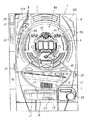
以下、図面を参照して、本発明の実施形態について説明する。まず、図1及び図2を参照して弾球遊技機1の全体の構成について説明する。図1は、実施形態に係る弾球遊技機1の正面図であり、図2は、弾球遊技機1の背面図である。
【0013】
弾球遊技機1は、縦長な方形状に枠組み形成される外枠2と、該外枠2の一側に開閉自在に軸支され且つ弾球遊技機1の主要構成部のほぼすべてが集約して設けられる枠基体3と、該枠基体3の前面上部に開閉自在に設けられるガラス板保持枠4と、から構成されている。枠基体3に設けられる主要構成部としては、ガラス板保持枠4、遊技盤40、上皿12、灰皿21を含む下皿18、操作ハンドル22、機構板50、打球発射装置71がある。また、図示の実施形態では、弾球遊技機1の側方に遊技者に遊技玉を貸し出すためのユニット装置としてのカードユニット装置30が付設されている。
【0014】
ガラス板保持枠4には、後述する遊技盤40の遊技領域をほぼ透視し得る円形透視窓5が開設され、該円形透視窓5の裏面からガラス板が装着されている。また、ガラス板保持枠4には、円形透視窓5の外周に沿って、その上部に装飾LED7が、その左右両側方に装飾蛍光灯6a・6bが設けられている。この装飾LED7や装飾蛍光灯6a・6bは、遊技状態に応じて点灯又は点滅されるものであり、特別の遊技状態の発生時や継続時を遊技者に報知すると共に遊技の雰囲気を盛り上げるものである。また、ガラス板保持枠4の軸支側上部には、払い出すべく景品玉が不足したことを報知する玉切れLED8や、入賞玉の発生に基づいて所定個数の景品玉が払い出されたことを報知する払出LED9が設けられ、更に、ガラス板保持枠4の上部左右に遊技の進行に応じた効果音を発生するスピーカ10a・10bが設けられている。なお、上記した構成のうち、装飾LED7や玉切れLED8及び払出LED9は、複数のLEDがプリント配線基板上に実装されるように構成されるものであるが、このプリント配線基板を金属ベースプリント配線基板で構成することにより、LEDから発生される熱の放熱効果を高めることができる。
【0015】
次に、ガラス板保持枠4の下部で開閉自在に取り付けられる上皿12の構成について説明すると、上皿12は、合成樹脂製の上皿開閉板11の表面に複数の合成樹脂製部材を組合せた皿部材を固着することにより構成されている。上皿開閉板11には、その開放側の上端に玉抜き操作レバー16が設けられている。この玉抜き操作レバー16は、左右方向に移動可能に設けられ、図示しないスプリングの付勢力に抗して一方向に移動させることにより、上皿12に貯留されていた玉を上皿開閉板11の裏面に形成される玉抜き路(図示しない)を流下させて下皿24に誘導するものである。また、上皿12には、その内部に圧電ブザー17が内蔵されている。この圧電ブザー17は、遊技玉の貸出異常が生じたとき(例えば、ピッ、ピッ、ピッという連続音)、あるいは遊技玉の貸出時(例えば、100円相当の遊技玉が払い出される毎にピーという音)に、その旨を報知する報知音が発生されるものである。
【0016】
上記した上皿12について、さらに詳細に説明すると、上皿12は、その上流側に形成される賞球払出口14とその下流側に形成される打球供給口15とを連絡するように貯留整列路13が形成されており、その貯留整列路13の中程底面裏面に上皿玉検出器(図示しない)が設けられている。この上皿玉検出器は、上皿12に残留する打玉を検出するものである。また、上皿12には、弾球遊技機1に隣接して設けられるカードユニット装置30を介して遊技玉を借り受ける際に操作する操作部が設けられている。なお、この操作部は、玉貸スイッチ、返却スイッチ、自動玉貸スイッチ、度数表示LED、及び自動玉貸表示LED(共に図示しない)から構成されている。玉貸スイッチは、カードユニット装置30によって遊技玉を借り受ける際に操作するものである。返却スイッチは、遊技終了の際にカードユニット装置30のカード挿入口33に差し込まれたカードを返却するためのものである。度数表示LEDは、カードユニット装置30のカード挿入口33に差し込まれたカードの残額が表示されるものである。また、自動玉貸スイッチは、借り受けるべき遊技玉を前記玉貸スイッチを操作して行うマニュアルモードと、上皿12の打玉の残量が前記上皿玉検出器によって検出されなくなったときに自動的に遊技玉を払い出す自動モードと、のいずれかのモードに設定するものであり、自動モータが選択設定されているときには、自動玉貸表示LEDが点灯している。
【0017】
しかして、後述する遊技盤40の遊技内容において大当り遊技状態が発生すると、短時間に多量の入賞玉を獲得するチャンスがある。このように大当り遊技状態という遊技者にとって極めて大きなチャンスは、上皿12の残留玉がほとんどなくなった時点で発生する場合もあり、このような場合、続けて打玉を発射させて打玉を可変入賞球装置42の特定入賞領域に入賞させる必要があるにも拘らず、打玉が上皿12に残存しないので、慌てて玉貸スイッチを操作して遊技玉を借り受けなければならない。しかし、玉貸スイッチを操作してから遊技玉が払い出され、しかもその玉が発射されて可変入賞球装置42の特定入賞領域に到達するまでに多少の時間がかかるため、その時間の間に有利なチャンス(継続権の成立)を逃してしまうという不都合があるが、本実施形態においては、自動玉貸スイッチを自動モードに設定しておけば、上皿玉検出器18が打玉の不存在を検出した時点で自動的に遊技玉を上皿12に払い出すので、上記したような不都合は生じない。なお、上皿12として上記した制御を行わないならば、上皿玉検出器及び自動玉貸スイッチを省略したものでも良い。
【0018】
また、枠基体3の下部に取り付けられる下皿18は、前記上皿12から溢れた賞球であって余剰玉通路(図示しない)を介して余剰玉払出口19から排出される余剰の賞球を貯留するものであり、その下皿18の前面壁には、玉抜き操作レバー20がスライド可能に取り付けられるようになっている。この玉抜き操作レバー20を操作することにより、下皿18に貯留されていた賞球を下方に玉抜きして持ち運び可能な玉箱に移し替えることができる。また、下皿の左側には、灰皿21が設けられ、右側には、操作ハンドル22が設けられている。操作ハンドル22は、後述する打球発射装置71の発射装置モータ72の駆動を開始せしめるメインスイッチ及びタッチアンテナ(共に図示しない)を内蔵していると共に、弾発力を調節するものである。
【0019】
弾球遊技機1の正面構造は、概ね上記した通りであるが、図示の実施形態では、弾球遊技機1にカードユニット装置30が隣接されている。このカードユニット装置30は、前記上皿12の上面に設けられる前述した操作部を操作することにより作動されるものである。しかして、カードユニット装置30は、使用可能状態であるか否かを表示する使用可能表示器31と、当該カードユニット装置30がいずれの側の弾球遊技機1に対応しているか否かを表示する連結台方向表示器32と、記録媒体としての磁気カードを挿入するカード投入口33とが設けられている。そして、このように構成されるカードユニット装置30は、独自の制御回路によって制御されるものであるが、上皿12に設けられる玉貸スイッチ、返却スイッチ、及び度数表示LEDや、後述する制御基板ボックス64内に収納された賞球払出制御基板63と接続されている。なお、カードユニット装置30を弾球遊技機1に内蔵しても良い。なお、本実施形態においては、遊技者に遊技玉を貸し出すためのユニット装置としてカードユニット装置30を例示したが、例えば、紙幣等を挿入し得るユニット装置であっても良い。
【0020】
次に、遊技盤40の正面構造について説明すると、遊技盤40は、前記枠基体3の裏面側に一体的に形成される遊技盤収納枠(図示しない)に収納固定されるべく、ほぼ正方形状の合板により形成され、その表面には、円形うず巻き状に誘導レール(図示しない)が取り付けられ、該誘導レールの内側が遊技領域とされて発射された打玉が落下するものである。遊技領域には、図示の場合、ドラム状可変表示装置41や可変入賞球装置42やドラム状可変表示装置41の可変表示を許容する始動入賞口43が設けられると共に、単に打玉を入賞とする入賞口44・45、打玉の流下方向及び速度を変化せしめる風車又は多数の障害釘が設けられ、また、遊技領域の最下方には、いずれの入賞領域にも入賞しない打玉が取り込まれるアウト口46が設けられている。
【0021】
一方、弾球遊技機1の裏面側には、図2に示すように、機構板50が開閉自在に設けられている。機構板50の中央には窓開口51が開設され、該窓開口51からは、前記遊技盤40の裏面に取り付けられた入賞玉集合カバー体52が貫通されている。入賞玉集合カバー体52には、中継基板53と、ドラム表示制御回路基板54を備えた前記ドラム状可変表示装置41と、が設けられている。なお、各基板53・54は、相互間で接続されている。また、中継基板53には、遊技盤40上の各種電気部品が接続されると共に、後述する遊技制御回路基板61が接続されている。一方、ドラム表示制御回路基板54には、前記可変表示装置41を構成する各種電気部品(ドラムモータ、ドラムランプ、ドラムセンサ等)が接続されると共に、遊技制御回路基板61が接続されている。
【0022】
また、前記機構板50には、発生した入賞玉に基づいて所定個数の賞球を払い出す玉タンク55と、賞球払出装置56と、玉タンク55内の玉を賞球払出装置56に送る玉整列レール57、カーブ樋58、及び通路体59と、玉止め部材60a及び入賞玉排出ソレノイド60bを備えた入賞玉処理装置60と、遊技制御回路基板61を収納した回路基板ボックス62と、賞球払出制御基板63を収納した制御基板ボックス64と、ユニット中継基板65を収納した中継基板ボックス66と、ターミナル基板67を収納したターミナル基板ボックス68と、が設けられている。遊技制御回路基板61は、CPU、RAM、及びROMを備えてドラム式可変表示装置41や可変入賞球装置42等の遊技装置の遊技動作を制御するものである。賞球払出制御基板63は、賞球払出装置56の動作を制御するものである。ユニット中継基板65は、弾球遊技機1とカードユニット装置30との配線を中継するものである。ターミナル基板67は、遊技制御回路基板61に電源を供給するものである。また、弾球遊技機1の裏面には、上記した機構板50以外の領域に、装飾制御基板69を収納した制御基板ボックス70と、発射装置モータ72を備えた打球発射装置71とが設けられている。装飾制御基板69は、遊技制御回路基板61からの指令又はデータに基づいて弾球遊技機1の前面に設けられる電気的装飾部品(ランプ等)の動作を制御するものである。
【0023】
なお、上記した各種基板及び装置には、所定の配線を接続するためのコネクタが設けられており、特に、ターミナル基板ボックス68に収納されるターミナル基板67は、遊技制御回路基板61に電源を供給するだけでなく、弾球遊技機1に設けられる各種電気的装置、例えば、上記した各基板及び打球発射装置71にも電源を供給すると共に、弾球遊技機1の内部での信号線の中継、あるいは弾球遊技機1と外部との信号線の中継を行うための端子も設けられている。
【0024】
次に、各種制御用の回路基板を収納してなる基板ボックスの構成について回路基板ボックス62を例に挙げて説明する。回路基板ボックス62は、図3に示すように、前記遊技制御回路基板61を内部に収納する蓋体80及びボックス本体100の組付体からなり、この組付体が取付台120を介して前記機構板50に取り付けられて構成される。先ず、ボックス62内に収納される遊技制御回路基板61について図6を参照して説明する。回路基板61は、図6に示すように、長方形状のプリント配線基板によって構成されており、その上面の大部分はROM等の電子部品73を実装する電子部品実装領域74として形成される一方、幅方向一側の領域がコネクタ75を実装するコネクタ実装領域76として形成されている。また、回路基板61には、幅方向一側の両端に止め穴77が穿設される一方、幅方向他側の両端には係合穴78が穿設されている。なお、回路基板61の上面及び下面における止め穴77の外周には、メッキ部79が設けられている。このメッキ部79は、回路基板61を後述の本体枠107にビス119止めする際、回路基板61のグランドライン61aと本体枠107とを導通させるためのものであり、ボックス62内で発生する静電気から回路基板61を保護するようになっている。
【0025】
蓋体80は、図4に示すように、透視性を有する上板81と、金属製の蓋枠86と、透視性及び導電性を有する導電板94と、を備えている。上板81は、透明合成樹脂の長方形板からなり、その下面側の外周端部には、所定間隔を置いて複数の溶着突起82が突設されている。また、上板81の長手方向の両端には、複数(実施形態中では、4つ)の取付片部83a〜83dが並設されている。取付片部83a〜83dには、相互間を連結する連結片89a〜89cが一体成形されている。なお、各取付片部83a〜83d間には、スリット状の溝が形成され、連結片89は、取付片部83a〜83dの外壁面から突出した状態で設けられている。連結片89の上方に位置する上板81の上壁部分には、溝部92が形成され、これによって各取付片部83a〜83dと対応する上板81の上壁部分は、切断可能な連結部81a〜81dとして形成されている。また、取付片部83a〜83dには、それぞれ取付穴99aが穿設されると共に、その取付穴99aの穿設部分を含む内壁側には係合突起99bが形成されている(図7(B)参照)。なお、この係合突起99bは、後述する蓋枠86側の切欠部86bとの係合により上板81と蓋枠86との取り付け強度を向上させると共に、ボックス本体100との組み付け状態でその内向面(係合突起99bの先端面)が後述する本体枠107の側壁外面と当接して隙間をなくすことにより、取付穴99aを止めるワンウェイネジ130の切断を防止するようになっている。また、取付片部83a〜83d及び取付片部83a〜83dと対応する上板81の上壁面には、図9(A)及び図10に示すように、それぞれ復元示唆用に「1〜4」の刻印131〜134が施されている。具体的には、取付片部83aに対応するものが「1」の刻印131であり、取付片部83bに対応するものが「2」の刻印132であり、取付片部83cに対応するものが「3」の刻印133であり、取付片部83cに対応するものが「4」の刻印134である。なお、取付片部83a〜83dは、上板81の長手方向の両端で非対称に設けられている。例えば、長手方向一端の取付片部83aと対向する位置には、長手方向他端の取付片部83dが配されており、長手方向一端の取付片部83dと対向する位置には、長手方向他端の取付片部83aが配されている。また、上板81の上面側の一部には、凹部85が形成されており、該凹部85には復元示唆シール84が貼着されている。復元示唆シール84には、図9(B)に示すように、回路基板ボックス62を開放した後に再度閉塞状態に復元する手順と、機種名(図9(B)中には「A」と記載)と、が記されている。なお、機種名シールを別途設けた構成としてもよい。また、回路基板ボックス62の復元手順は後で詳述する。
【0026】
蓋枠86は、上面に開口部87を有すると共に、その外周縁部には全周に亘って側壁を有する形状となっている。なお、幅方向の一側壁は、その他の側壁に比べて下方に突出して設けられ、回路基板61の収納状態で電子部品実装領域74とコネクタ実装領域76とを蓋枠86の内外に仕切る仕切り壁86aとして形成されている(図7(A)参照)。開口部87以外となる残りの上面領域には、上板81側の複数の溶着突起82を個々に挿通する挿通穴88が複数穿設され、長手方向両端の側壁には、上板81との組み付け状態で取付片部83a〜83dの各係合突起99bを個々に係止する切欠部86bが並設されている。一方、仕切り壁86aが形成された幅方向側壁には、収納する回路基板61からの発熱を外部に放出するための放熱穴91が穿設されている。また、仕切り壁86aが形成さない蓋枠86の幅方向側壁には、取付穴90が穿設されている。この取付穴90は、後で詳述するボックス本体100との組み付け時にビス(皿ネジ)93の頭部が蓋枠86の側壁面に入り込むようなテーパー形状をなしている。
【0027】
導電板94は、上板81と同様に透明合成樹脂の長方形板からなり、その上面側には黒色塗装を施した導電性繊維95が全域に接合して設けられている。導電板94の外周端部には、蓋枠86に穿設された挿通穴88と同様に、上板81側の溶着突起82を個々に挿通する挿通穴96が複数穿設されている。ここで、導電性繊維について簡単に説明すると、導電性繊維は、大きく分けて金属製(銅、黄銅、ニッケル、アルミニューム等)のフィラメントを網状に織ったものと、合成繊維に導電性粒子(銅、カーボン等)を塗布又は含浸させたものと、があり、いずれの種類の導電性繊維においても、電磁シールド効果及び光線透過率の見地から、50〜250メッシュ(特に、100〜200メッシュがよい)程度で、その開口率10〜90%(特に、30〜80%がよい)であることが望ましい。そして、メッシュという構造上、どうしても透視性が悪くなるが、本実施形態では、これを抑制するために、導電性繊維95を金属色を避けた濃色(実施形態中では、黒色)にすることで透視性を向上させている。
【0028】
なお、本実施形態では、透明合成樹脂板に導電性繊維95を接合することで導電板94を構成しているが、導電板の構成はこれに限定するものではなく、透明合成樹脂板に導電性繊維を埋設して導電板(俗にCRTフィルターなどともいう)を構成してもよい。この場合、その透明合成樹脂板を濃色とすることにより透視性を向上させることができる。また、透明導電層の形成によって導電板を構成してもよい。この透明導電層について簡単に説明すると、透明導電層は、金、白金、銀、錫、アルミニウム、ニッケル、パラジウム、あるいはアンチモン等の金属や酸化インジウムあるいは酸化錫等の金属酸化物、又はこれらの混合物を真空蒸着、スパッタリング、イオンプレーティング、CVD等の方法により導電性と透視性を有する厚みの層として樹脂材等の表面に形成されるものである。透明導電層の厚みは、通常5〜1000nm程度であり、その電気伝導性は、10000Ω/□以下、好ましくは1000Ω/□以下の電気抵抗率が適当である。
【0029】
しかして、蓋体80は、図5(A)(B)に示すように、蓋枠86の挿通穴88及び導電板94の挿通穴96を挿通した上板81の溶着突起82が超音波溶着されることで、上板81、蓋枠86、及び導電板94の組付体として構成されている。また、このような溶着突起82の溶着により、導電板94の導電性繊維95は、蓋枠86と確実に導通される。なお、溶着突起82の溶着において、上板81(溶着突起82)と導電板94とを同一素材で形成した場合には、溶着突起82の溶着部分が導電板94に混じり合い、より一層強固な溶着が可能になる。また、蓋体80の組み付け方法は、超音波溶着以外にも熱溶着したり、溶剤又は接着剤を用いてもよい。また、このような蓋体80の組み付け状態において、上板81側の係合突起99bは、蓋枠86側の切欠部114と係合した状態にある。また、上板81の上面と蓋枠86の側面との間には、長方形状のホログラムシール98が貼着されており、これによって蓋体80の組み付け状態が担保されている。
【0030】
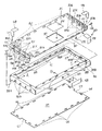
一方、ボックス本体100は、図6に示すように、透視性を有する底板101と、金属製の本体枠107と、を備えている。底板101は、透明合成樹脂の長方形板からなり、その上面側には、回路基板61の下面を支承するためのフランジ片102が四隅近傍部及び幅方向の両端中央部に立設されている。なお、幅方向一側の二隅近傍部に立設されたフランジ片102には、後述する係合片113との干渉を逃がすためのスリット部103が形成されている。一方、底板101の下面側には、本体枠107との間で所定間隔を保持するためのフランジ片104が立設されている。また、底板101には、幅方向他側の各隅角部及び長手方向一側のほぼ中央部にそれぞれ切欠部105a・105b・106が穿設されている。切欠部105a・105bは、回路基板61のビス止め部分との干渉を逃がすための切り欠きであり、切欠部106は、取付台120への取り付け状態で後述する係合突起124との干渉を逃がすための切り欠きである。
【0031】
本体枠107は、下面に開口部108を有すると共に、その外周縁部には全周に亘って側壁を有する形状となっている。開口部108の内周縁部には、その幅方向両側に断面L字状をなす係合片109が所定の条設長さで形成され、内周縁部の長手方向一側には、係止穴110aを穿設した係止片110が形成されている。また、開口部108以外となる残りの下面領域には、楕円形状をなす複数の透視穴111が穿設されている。下面領域における幅方向一側の両端には、取付穴112aを穿設した取付片112が形成され、下面領域における幅方向他側の両端には、係合突起113aを備えた係合片113が形成されている。また、上記した係合片109は、後で詳述する取付台120への取り付け時に取付台120側の係合レール121と係合し易いように先端部分が若干下方に折曲されている。
【0032】
一方、本体枠107の幅方向一側壁には、取付穴114aを穿設した取付片114が断面L字状をなして内向側に折曲形成されると共に、複数の放熱穴115が穿設されている。本体枠107の長手方向の両側壁には、上板81側の各取付片部83a〜83dの取付穴99aと対応する複数(4つ)の取付穴116が穿設されている。また、本体枠107の幅方向の両側壁には、その長手方向の両端部に補強片118が延設されている。この補強片118は、延設部分から内向側に折曲されることで本体枠107の長手方向両側壁を内側から押さえ、本体枠107の強度を向上するようになっている。また、側壁間の隙間を塞ぐので、側壁間を広げて不正に改造しようとしてもできない。なお、このような補強片は、本体枠107に限らず蓋枠86側に設けてもよい。
【0033】
しかして、上記した蓋体80及びボックス本体100は、以下に示す組み付けによって回路基板61を収納した組付体(回路基板ボックス62)として構成される。先ず、回路基板61と底板101とを重畳して本体枠107に装着する。そして、回路基板61の係合穴78に係合片113の係合突起113aを挿通する一方、回路基板61の止め穴77を取付片112の取付穴112aにビス119止めすることで、底板101を挟んで本体枠107に回路基板61を固定する。また、このような回路基板61の取り付け固定において、止め穴77と取付穴112aとの穴位置を合せる際、回路基板61が若干ズレることで係合突起113aと係合穴78とが係合し、ビス止めされない回路基板61の幅方向一側も固定される。
【0034】
次に、上面が開放しているボックス本体100に蓋体80を被せる。このとき、蓋体80の仕切り壁86aは、回路基板61の電子部品実装領域74とコネクタ実装領域76とを蓋枠86の内外に仕切った状態にある。これにより、蓋体80を取り外すことなく、コネクタ75への配線取り付け及び配線取り外しが可能になる。そして、図4及び図6に示すB方向において、蓋枠86の取付穴90と本体枠107の取付穴114aとをビス93で共締めし、そのビス93止め部分を長方形状のホログラムシール98で封印する。また、図4及び図6に示すA・Cの2方向において、取付片部83aの取付穴99aと本体枠107の取付穴116とをワンウェイネジ(ビス)130で共締めし(図7(B)参照)、そのビス130止め部分を長方形状のホログラムシール98で封印する。これにより、蓋体80とボックス本体100との内部空間に回路基板61を止着状態にて収納した組付体(回路基板ボックス62)が構成される。また、このような蓋体80とボックス本体100との組み付け状態において、各取付片部83a〜83d間のスリット状溝には、ワンウェイネジ130が螺着されずに予備的に取り付けられている。なお、ワンウェイネジ130は、ネジ130締め方向にしか回らない特殊なネジであり、一旦締め付けるとネジ130を破壊しない限り取り外すことができない。具体的には、図8に示すように、その頭部130aに設けられたネジ溝が当接面部130bと凹部130cとから構成されている。これにより、マイナスドライバーでネジ130締めを行う場合には、マイナスドライバーが当接面部130bと当接することで、一方向(図8(A)の時計回り方向)に頭部130aが回転してネジ130締めが行われる。一方、マイナスドライバーで頭部130aを他方向(図8(A)の反時計回り方向)に回転させてネジ130を取り外そうとした場合には、マイナスドライバーが凹部130cに入り込んで滑ってしまい頭部130aを回転させることができず、ひいてはネジ130を取り外すことができない。
【0035】
また、上記した蓋体80及びボックス本体100の組み付けを行うビス93・130は、それぞれ螺着状態で蓋枠86の側壁面に入り込む構成となっている。このため、ビス93・130止め部分を封印するホログラムシール98は、突起のない平坦面上に貼付され、シール98の剥れ及び損傷が防止できると共に、シール98に対する不正行為の判別が容易になる。ここで、ホログラムシールについて簡単に説明すると、ホログラムシールは、ホログラム層と光反射層と接着剤層とを備え、ホログラム層に形成されるホログラム図柄を偽造困難な図柄に構成することで、不正行為に伴うシールの貼り替えを防止するようになっている。このホログラム図柄は、ホログラムシールの表面に入射したコヒーレント光(レーザー光)がホログラム層のエンボス面を透して光反射層に入り、光反射層からホログラム干渉光としてホログラムシールの外方に反射されることで形成される。また、ホログラムシールを剥した場合は、もう一度貼り直してもホログラム図柄が元の形状にならないので、剥した痕跡が残る。
【0036】
以上のように、回路基板ボックス62は、蓋体80とボックス本体100とのビス93・130止め部分をホログラムシール98で封印することにより回路基板61の被覆状態を担保している。また、ボックス62内に設けられた導電板94によって電磁シールド効果を奏し得るようになっている。さらに、回路基板ボックス62は、その上壁面を構成する上板81と導電板94、及び下壁面を構成する底板101をそれぞれ透視性を有する素材から形成することで、回路基板61の実装面(上面)及びハンダ面(下面)を外部から透視できるようにしている。このため、回路基板61に不正な工作(例えば、ジャンパー配線を接続したり、電子部品を実装したりする不正工作)が施された場合には、直ちにその不正工作が判るようになっている。
【0037】
次に、上記した回路基板ボックス62を機構板50に取り付けるための取付台120について図3を参照して説明する。取付台120は、図3に示すように、合成樹脂(金属でもよい)によって形成された長方形板からなり、その基板中央には断面逆L字状をなす一対の係合レール121が所定間隔を置いて条設されている。なお、係合レール121の条設方向は、取付台120の長辺部に沿った左右方向となっている。取付台120の各長辺部(前後端縁)には、基板面に対して直交するガイド片122が突設されている。取付台120の右側端部には、弾性変形する解除レバー123が形成されており、該解除レバー123の基部には、ボックス本体100側の係止穴110aと係合する係合突起124が突設されている。また、取付台120の基板面には、機構板50側の取付ボス(図示しない)に取付台120をビス止めするための止め穴125が穿設されている。
【0038】
しかして、上記した取付台120は、止め穴125を介して機構板50にビス止めされることで機構板50上の所定部位に固定される。また、この取付台120に回路基板ボックス62を取り付けるときには、取付台120に対してボックス62を左側方からスライド装着させる。このとき、取付台120側の係合レール121は、ボックス62側の係合片109と係合した状態にあり、ガイド片122は、ボックス62のスライド移動を案内する。そして、このようなボックス62のスライド移動によって取付台120側の解除レバー123が下方に弾性変形し、遂には、ボックス62側の係止穴110aが取付台120側の係合突起124と係合してボックス62の装着が完了する。一方、回路基板ボックス62を取付台120から取り外すときには、解除レバー123を下方に押して係止穴110aと係合突起124との係合を解除し、この状態からボックス62を左側方にスライドさせることで簡単に取り外すことができる。即ち、回路基板ボックス62は、機構板50にビス止め固定された取付台120に対して着脱自在な構成となっている。
【0039】
次に、上記した回路基板ボックス62を回路基板61の検査(出荷納入後にROMが正規のものか否かを検査する)等で開放した後に再度閉塞状態に復元する手順を図10に基づいて説明する。先ず、図10(A)に示す回路基板ボックス62の閉塞状態において、取付穴90に貼着されたホログラムシール98を剥した後にビス93を取り外し、また、取付片部83aに貼着されたホログラムシール98を剥した後に「1」の刻印131を目印に連結部81aと連結片89aとをニッパー等の切断工具で切断する。これにより、取付片部83aは、蓋体80から完全に分離され且つワンウェイネジ130によってボックス本体100に固着された状態となる。即ち、ボックス本体100に対する蓋体80の固着が全て解除されて、回路基板ボックス62の開放が可能になる。なお、このとき、取付片部83aは、係合突起99bが本体枠107の外壁面と当接した状態にあり、ボックス本体100への固着状態がより一層強固なものとなっている。そして、図10(B)に示すように、ボックス本体100から蓋体80を取り外して回路基板61の検査等を行う。また、このような蓋体80の取り外し時(取付片部83aの切断時)、各取付片部83a・83b間のスリット状溝に予備的に取り付けられたワンウェイネジ130が取り出される。その後、回路基板ボックス62を閉塞するときには、蓋体80をボックス本体100に被せた状態で、取付穴90にビス93を螺着し、その螺着部分に新しいホログラムシール98を貼着する。また、取り出されたワンウェイネジ130を「2」の刻印132を目印に取付片部83bの取付穴99aに螺着する。これにより、取付片部83bの取付穴99aとこれに対応する本体枠107の取付穴116とがワンウェイネジ130によって共締めされる。そして、この取付片部83bの共締め部分に新しいホログラムシール98を貼着することで、回路基板ボックス62が再度閉塞状態に復元される。
【0040】
その後、回路基板ボックス62を再度開放(2回目の開放)して閉塞状態に復元する場合には、取付穴90に貼着されたホログラムシール98を剥した後にビス93を取り外し、「2」の刻印132を目印に連結部81bと連結片89bとを切断工具で切断することで、取付片部83bを蓋体80から分離させて回路基板ボックス62を開放する。後は同様に、取付穴90にビス93を螺着してその螺着部分に新しいホログラムシール98を貼着し、また、取付片部83bの切断に伴って取り出されたワンウェイネジ130を「3」の刻印133を目印に取付片部83cの取付穴99aに螺着し、新しいホログラムシール98を貼着する。これにより、回路基板ボックス62が再度閉塞状態に復元される。それ以降、回路基板ボックス62を開放(3回目の開放)して閉塞状態に復元する場合には、取付穴90に貼着されたホログラムシール98を剥した後にビス93を取り外し、「3」の刻印133を目印に連結部81cと連結片89cとを切断工具で切断することで、取付片部83cを蓋体80から分離させて回路基板ボックス62を開放し、取付穴90にビス93を螺着してその螺着部分に新しいホログラムシール98を貼着すると共に、取付片部83cの切断に伴って取り出されたワンウェイネジ130を「4」の刻印134を目印に取付片部83dの取付穴99aに螺着して新しいホログラムシール98を貼着する。その後の回路基板ボックス62の開放(4回目の開放)については、全ての取付片部83a〜83dが蓋体80から切り離された状態となるため、回路基板ボックス62を開放するだけで閉塞状態に復元することはできない。
【0041】
ところで、上記した回路基板ボックス62の閉塞状態においては、連結部81a〜81d乃至連結片89a〜89cを切断して取付片部83a〜83dと上板81との連結を解除しない限り、回路基板ボックス62が開放できないようになっている。従って、回路基板61の検査以外で連結部81a〜81d乃至連結片89a〜89cが切断されるような場合は、この切断により回路基板61に不正が行われたことが即座に且つ確実に判別できるため、回路基板ボックス62の防犯効果を高めることができる。また、回路基板ボックス62の構成では、上板81の溶着突起82を切り離しても、上板81は、取付片部83aのビス130止めにより取り外すことができず、然も導電板94が回路基板61上に落ち込む。このため、溶着突起82を切り離した隙間から回路基板61に細工をしようとしても導電板94がそれを阻止する。また、ホログラムシール98を剥してビス93を外した場合には、ホログラムシール98の痕跡がしっかりと残るため不正が行われたことが即座に分かる。また、回路基板ボックス62の復元において、蓋体80のビス130止め箇所は、図9(A)に示すように、蓋体80を平面から見て対角線上になるように設定されている。このため、ビス130止め箇所を蓋体80の一側に偏らせることがないので、開放後に復元した回路基板ボックス62でも防犯効果の高さを維持することができる。
【0042】
以上のように、本実施形態に係る回路基板ボックス62は、ボックス本体100と蓋体80とを備え、ボックス本体100及び蓋体80のうち少なくとも一方には、ワンウェイネジ130により前記ボックス本体100と前記蓋体80とを固着状態に取り付ける第一の取付片部83aと、該取付片部83aを切り離して前記ボックス本体100と前記蓋体80との固着状態を解除する連結部81a及び連結片89aと、該連結部81a及び連結片89aの切断状態でワンウェイネジ130により前記ボックス本体100と前記蓋体80とを再び固着状態に取り付ける第二の取付片部83b〜83dと、該取付片部83b〜83dを切り離して前記ボックス本体100と前記蓋体80との固着状態を解除する連結部81b〜81d及び連結片89b・89cと、が形成され、前記取付片部83a〜83dを集約的に設けたことを特徴とする。このように構成することにより、出荷納入後に回路基板61を検査する場合でも、取付片部83b〜83dをワンウェイネジ130で固着することにより、別の新しい回路基板ボックスに取り替えることなく、再度防犯効果の高い回路基板ボックス62に復元することができる。また、このような構成では、複数の取付片部83a〜83dを集約的に設けることにより、固着状態にある取付片部が一瞥できるので、回路基板ボックス62の開閉作業が容易になり、検査の迅速化を招来することができる。
【0043】
また、前記ワンウェイネジ130は、回路基板ボックス62に複数(3個)装備されると共に、前記取付片部83b〜83dの切り離し毎に1つずつ取り出される構成としたので、蓋体80とボックス本体100との固着状態を解除する作業が容易になり、然も蓋体80とボックス本体100とを固着するためのワンウェイネジ130を事前に用意しておく必要がないので、回路基板ボックス62の復元作業が行い易くなる。
【0044】
また、前記取付片部83a〜83dは、前記連結片89a〜89cを介して並設され、前記ワンウェイネジ130は、前記連結片89a〜89cが切断されることによって取り出される構成としたので、連結片89a〜89cを切断した時点でボックス本体100と蓋体80とを固着するワンウェイネジ130が取り出されるので、ボックス本体100と蓋体80との固着作業及びその解除作業が容易になる。
【0045】
また、前記ボックス本体100及び前記蓋体80を固着状態とする前記取付片部83a〜83dの外壁面が平坦になるようにし、その外壁面に封印部材(ホログラムシール98)を貼着したので、回路基板ボックス62の閉塞状態をホログラムシール98で担保することができ、また、そのホログラムシール98は、突起のない平坦面上に貼付されるのでシール98の剥れ及び損傷が防止できると共にシール98に対する不正行為の判別が容易になる。
【0046】
また、取付状態において、前記蓋体80が表面側になるように取り付けられ、その蓋体80にのみ前記取付片部83a〜83dを形成したので、回路基板ボックス62の外壁面に取付片部83a〜83dを配した構成となるので、取付片部83a〜83dを切り離したことがよく分かる。
【0047】
また、前記連結片89a〜89cは、その並設方向と直交する方向に切断し易い構造としたので、1つの連結片を切断する際、同時に他の連結片まで切断する虞がない。
【0048】
また、前記取付片部83a〜83dは、平板状で且つ回路基板ボックス62の側面に沿って形成された構成としたので、取付片部83a〜83dが突出しないので破損などを防止することができる。
【0049】
また、前記蓋体80は、金属製の蓋枠86と合成樹脂製の上板81とを備え、該上板81に前記取付片部83a〜83dを形成したので、取付片部83a〜83dを合成樹脂で形成することによりその切り離し作業を容易にすることができる一方、蓋体80の一部に金属を使用することで強度を向上することができる。また、このように蓋体80の一部に金属を使用することで、静電気に強い回路基板ボックス62を構成することができる。
【0050】
なお、上記した実施形態では、本発明における複数の取付部(取付片部83a〜83d)の集約箇所を回路基板ボックスの2箇所(二側辺)としているが、この構成に限定するものではない。例えば、蓋体の一側をボックス本体に対して回動自在に軸支し、その開放側の1箇所に取付部を集約的に設けてもよく、さらには2箇所以上の複数箇所に複数の取付部を集約して設けてもよい。また、集約して設ける部位についても特に限定しない。例えば、回路基板ボックスの側面部分でなく上面部分でもよく、切り離し易いように外側に突出して設けたり、切断部を突出させてもよい。但し、本実施形態のように取付部を突出させずに設けた場合は、取付部を破損し難い構成とすることができる。また、取付部は切断後に回路基板ボックスの一部として残るようにしてもよいし、残らないようにしてもよい。また、ワンウェイネジの螺着方向は特に限定しない。
【0051】
また、取付部の集約も並列的なものに限定しない。例えば、回路基板ボックスの閉塞状態で回路基板のROMの上方に位置する蓋体部分に開口を設けると共に、該開口を四角形状の平板で閉塞し、その平板の全側辺に設けた取付部のうち対向する二側辺の取付部を固着するようにしてもよい。また、取付部の材質は、金属や合成樹脂などいずれの材質であってもよいが、望ましくは切断させ易い合成樹脂がよい。また、出荷納入時点で蓋体とボックス本体とを固着する第一及び第二の固着手段は、ワンウェイネジに限らず、溶着であれば溶着するための溶剤であり、接着であれば接着剤である。また、切り離し可能な取付部は、必ずしも蓋体側に設ける必要はなく、ボックス本体側に設けたり、あるいは蓋体とボックス本体との両側に設けた構成としてもよい。また、回路基板ボックスに装備されるビスの装備箇所は、例えば、取付部の裏面側としてもよい。
【0052】
また、上記した実施形態では、蓋体80から切断可能な取付片部を4つ並設することで、回路基板ボックス62の4回の開放と3回の復元とを可能にしているが、取付片部は複数であればいずれの並設個数であってもよい。但し、並設個数を多く設定すればする程、回路基板ボックスの開放回数と復元回数とをより多くすることができる。また、本実施形態では、締まる方向にしか回らないワンウェイネジ130で取付片部83a〜83dを締め付ける構成となっているが、これに替えて破断取付ネジやリベット等で取付片部83a〜83dを締め付ける構成としてもよい。また、取付片部83a〜83dは、溶着や接着によって取り外しできないようにしてもよい。また、取付片部83b〜83dのワンウェイネジ130は、必ずしも回路基板ボックス62に装備させる必要はなく、検査時に支給するものであってもよい。また、実施形態中では、復元内容(手順)を示唆する本発明の示唆内容表示部を復元示唆シール84及び刻印131〜134としているが、復元示唆シール84の内容を回路基板ボックス62の外壁面に刻印したものであってもよい。また、実施形態中では、取付片部83a〜83dが形成された蓋体80の二側辺を平行する二側辺とすると共に、蓋体80のビス130止め箇所を対角線上になるように設定しているが、この構成に限定するものではない。即ち、固着状態の復元を複数回行う場合、蓋体の一側辺で取付部を固着していく方向と、蓋体の他側辺で取付部を固着していく方向と、を逆方向にした構成であればよく、この構成にすることで、ビス130止め箇所を蓋体80の一側に偏らせることなく、開放後に復元した回路基板ボックス62でも防犯効果の高さを維持することができる。
【0053】
また、上記した実施形態では、本発明の基板収納ボックスを弾球遊技機用の遊技制御回路基板を収納する回路基板ボックスとしているが、これに限定するものではない。例えば、賞球払出制御基板などを収納する基板収納ボックスでもよい。即ち、内部の回路基板に対する不正行為を防止する必要がある基板収納ボックスであればよい。また、遊技機としては、弾球遊技機以外の遊技機(例えば、スロットマシンやコインゲーム等)であってもよい。さらには、各種構成部材を形成する素材については、取り分け実施形態中に記載のものに限定するものではない。例えば、透視性を有する上板を透明合成樹脂ではなく、ガラス素材から形成してもよい。
【0054】
なお、以上説明した実施形態から把握できる発明又は変形例として以下のものがある。
(1)回路基板を被覆状態にて収納する遊技機の基板収納ボックスにおいて、前記回路基板を取り付けるボックス本体と、該ボックス本体を上方から覆う蓋体と、を備え、前記ボックス本体を金属平板から折曲形成すると共に、その折曲形成したボックス本体の側壁を溶接することなく前記蓋体の側壁に固着したことを特徴とする遊技機の基板収納ボックス。このように構成することにより、基板収納ボックスとしての強度を保証した上で溶接コストを削減することができる。
(2)回路基板を被覆状態にて収納する遊技機の基板収納ボックスにおいて、前記回路基板を取り付けるボックス本体と、該ボックス本体を上方から覆う蓋体と、を備え、前記蓋体を金属平板から折曲形成すると共に、その折曲形成した蓋体の側壁を溶接することなく前記ボックス本体の側壁に固着したことを特徴とする遊技機の基板収納ボックス。このように構成することにより、基板収納ボックスとしての強度を保証した上で溶接コストを削減することができる。
(3)透視板は、蓋枠に取り付けられる方が組み付け易いので望ましいが、透視板をボックス本体側に取り付けるようにして、ボックス本体と蓋体とを分離させなければ透視板が取れないものでも本実施形態と同様の効果が得られる。蓋体とボックス本体との固着を解除して初めて透視板をボックス本体から取り外し得る構成としたことを特徴とする遊技機の基板収納ボックス。
(4)本実施形態では、底板を用いて基板の底側を見えるようにしたが、底板がなくボックス本体の底面に大きな開口がないもの、つまり、上面を開放した箱状の本体枠のみのものでもよい。また、導電板がないものでもよく、透視板は、蓋枠の上下どちらに取り付けられるものでもよい。
(5)封印部材は、ホログラムシールに限定することなく、痕跡(剥した跡など)が残るものであればよい。例えば、色が変わったり一部が剥れずに残るものなど。
(6)ホログラムシール(封印部材)が透視板と蓋体とに跨がって貼付されるか、又は透視板と蓋体と取付基板(本体枠)とに跨がって貼付されるものであれば、そのシール(封印部材)が固着部に貼付されていないものでもよく、特に貼付する位置は限定しない。また、固着部に貼付されるシール(封印部材)と、透視板及び蓋体に跨がって貼付されるシール(封印部材)と、は別体でもよい。
(7)ワンウェイネジ以外のネジ止めもしているが、ネジ止めは、ワンウェイネジ(破壊して初めて取り外し可能な固着手段)のみのものでもよい。また、ネジ止め以外の係止部があってもよい。
(8)蓋体と透視板との取り付けは、ネジ止めに限らず、はまり込んで係止するものでもよい。
(9)蓋枠及び本体枠は、合成樹脂製のものでもよく、さらには導電性のものが好ましい。
(10)封印部材は、ビス自体に貼付しないものでもよいし、取付片部の連結部に貼付しないものでもよい。
(11)連結片に切断順序を示唆する番号を刻印してもよく、また切断すべき部分を着色するなどしてもよい。なお、連結片に切断順序を刻印した場合には、連結片を切断した時点で刻印が破断し、連結片が切断されていることを明確にすることができる。
(12)取り出されるビスの径と取付穴の径とを異ならせて、1つの取付穴に対して1つのビスしか取り付かないようにしてもよい。また、ビスとビス穴に色を付けてビス止め部分を分かり易くしてもよい。
【0055】
【発明の効果】
以上、説明したところから明らかなように、本発明の請求項1においては、回路基板を収納する基体及び蓋体を備えた遊技機の基板収納ボックスにおいて、前記蓋体に設けられ、前記基体と前記蓋体とを固着させる固着手段が取り付けられる第一の取付片部と、前記第一の取付片部を前記蓋体から切り離して前記基体と前記蓋体との固着状態を解除するために切断される第一の切断部と、前記第一の切断部が切断され、前記第一の取付片部が前記蓋体から切り離されて前記基体と前記蓋体との固着状態が解除されても再び前記基体と前記蓋体とを固着させる固着手段が取り付けられる第二の取付片部と、前記第二の取付片部を前記蓋体から切り離して前記基体と前記蓋体との固着状態を解除するために切断される第二の切断部と、前記第二の取付片部に取り付けられる予備の固着手段が保持される予備保持部と、が形成され、前記第一及び第二の取付片部を並設させて前記蓋体の平行に対向する二側辺に各々設けたことを特徴とする。このように構成することにより、出荷納入後に回路基板を検査する場合でも、取付部を第二の固着手段で固着することにより、別の新しい基板収納ボックスに取り替えることなく、再度防犯効果の高い基板収納ボックスに復元することができる。さらに、複数回検査しても防犯効果を高く維持することができる。また、このような構成では、複数の取付部を蓋体の平行に対向する二側辺に各々設けることにより、固着状態にある取付部が一瞥できるので、基板収納ボックスの開閉作業が容易になり、検査の迅速化を招来することができる。
【0056】
また、前記第二の固着手段は、基板収納ボックスに複数装備されるので、蓋体と基体とを固着するための第二の固着手段を事前に用意しておく必要がないため、基板収納ボックスの復元作業が行い易くなる。
【0057】
【0058】
【0059】
【0060】
【0061】
【0062】
【図面の簡単な説明】
【図1】 本発明の一実施形態における弾球遊技機を示す正面図である。
【図2】 弾球遊技機を示す背面図である。
【図3】 回路基板ボックス及び取付台を示す斜視図である。
【図4】 蓋体を示す分解斜視図である。
【図5】 同図(A)(B)はそれぞれ溶着突起の溶着状態を示す説明図である。
【図6】 蓋枠を示す展開図である。
【図7】 同図(A)は蓋体とボックス本体との組み付け状態を示す縦断面図であり、同図(B)はワンウェイネジによって蓋体をボックス本体に組み付けた状態を示す部分断面図である。
【図8】 同図(A)(B)はそれぞれワンウェイネジを示す説明図である。
【図9】 同図(A)は「1〜4」の刻印が施された回路基板ボックスを示す平面図であり、同図(B)は復元示唆シールを示す平面図である。
【図10】 同図(A)〜(C)はそれぞれ回路基板ボックスの復元手順を示す側面図である。
【符号の説明】
1 弾球遊技機
40 遊技盤
50 機構板
61 遊技制御回路基板(回路基板)
62 回路基板ボックス(基板収納ボックス)
80 蓋体
81 上板
81a 連結部(第一の切断部)
81b〜81d 連結部(第二の切断部)
82 溶着突起
83a 取付片部(第一の取付片部)
83b〜83d 取付片部(第二の取付片部)
84 復元示唆シール
86 蓋枠
89a 連結片(第一の切断部)
89b・89c 連結片(第二の切断部)
94 導電板
95 導電性繊維
98 ホログラムシール(封印部材)
99a 取付穴
99b 係合突起
100 ボックス本体(基体)
101 底板
107 本体枠
116 取付穴
120 取付台
130 ワンウェイネジ(第一及び第二の固着手段)
131〜134 刻印
[0001]
BACKGROUND OF THE INVENTION
The present invention relates to a board storage box of a gaming machine that stores a circuit board in a covered state.
[0002]
[Prior art]
Conventionally, many circuit boards are provided in pachinko gaming machines and slot machines. In particular, a lot of electronic elements such as MPU, ROM, and RAM constituting a microcomputer are mounted on a game control circuit board that controls game operations. In many cases, it is possible to realize different game contents by exchanging the ROM storing the program for controlling the game operation. For this reason, the game control circuit board is usually housed and provided in a resin box in order to prevent fraud. This board storage box is composed of a box body to which a circuit board is attached and a cover body covering the circuit board. The cover body is fixed to the box body with a one-way screw so that the board storage box itself is not destroyed. It was a configuration that could not be opened as much as possible, and increased the crime prevention effect to prevent fraud against the circuit board (unauthorized work connecting jumper wiring or mounting electronic components).
[0003]
[Problems to be solved by the invention]
However, in the conventional board storage box, when the circuit board was inspected after delivery, it was necessary to destroy the board storage box, so it was necessary to replace it with another new board storage box in one inspection. . The present invention has been made in view of the above-described circumstances, and the object of the present invention is to quickly provide a board storage box having a high crime prevention effect without replacing it with another new circuit board box even when inspecting the circuit board. An object of the present invention is to provide a board storage box for a gaming machine that can be restored.
[0004]
[Means for Solving the Problems]
In order to achieve the above object, the solution adopted by claim 1 of the present invention is that a base body (box body) for housing a circuit board (game control circuit board 61) as shown in FIGS. 100) and a board storage box (circuit board box 62) of a gaming machine (bullet ball gaming machine 1) provided with a lid 80, provided on the lid 80, to fix the base body 100 and the lid 80 together. The first attachment piece 83a to which the fixing means (one-way screw 130) is attached and the first attachment piece 83a are separated from the lid body 80 to release the adhesion state of the base body 100 and the lid body 80. Therefore, the first cutting portion (the connecting portion 81a and the connecting piece 89a) to be cut and the first cutting portions 81a and 89a are cut, and the first mounting piece portion 83a is cut off from the lid body 80. The group Second mounting pieces 83b to 83d to which fixing means (one-way screw 130) for fixing the base body 100 and the lid body 80 again is attached even if the adhesive state between the lid 100 and the lid body 80 is released; The second attachment pieces 83b to 83d are separated from the lid body 80, and the second cutting portions (the coupling portions 81b to 81d and the coupling portions are cut to release the fixed state between the base body 100 and the lid body 80). Pieces 89b and 89c) and a preliminary holding portion (slit-like groove between the mounting pieces 83a to 83d) for holding a preliminary fixing means (one-way screw 130) attached to the second mounting pieces 83b to 83d. And the first and second attachment pieces 83a to 83d are arranged side by side to form the lid 80. In parallel Each of the two opposing sides is provided. With this configuration, even when the circuit board 61 is inspected after delivery, the mounting pieces 83b to 83d are fixed with the one-way screws 130, so that the crime prevention effect can be obtained again without replacing with another new circuit board box. The circuit board box 62 having a high height can be restored. Furthermore, even if it inspects several times, the crime prevention effect can be maintained high. In such a configuration, the plurality of attachment pieces 83 a to 83 d are attached to the lid 80. In parallel By providing each on the two opposing sides, the mounting pieces in the fixed state can be gathered together, so that the circuit board box 62 can be easily opened and closed, and the inspection can be speeded up.
[0005]
In addition, as shown in FIG. 10, a plurality (three) of the one-way screws 130 are installed in the circuit board box 62. So the lid There is no need to prepare a one-way screw 130 for fixing the body 80 and the box body 100 in advance. For The restoration work of the circuit board box 62 is facilitated.
[0006]
[0007]
[0008]
[0009]
[0010]
[0011]
[0012]
DETAILED DESCRIPTION OF THE INVENTION
Embodiments of the present invention will be described below with reference to the drawings. First, the overall configuration of the ball game machine 1 will be described with reference to FIGS. 1 and 2. FIG. 1 is a front view of a ball game machine 1 according to the embodiment, and FIG. 2 is a rear view of the ball game machine 1.
[0013]
The ball game machine 1 includes an outer frame 2 that is formed into a vertically long rectangular frame, and is pivotally supported on one side of the outer frame 2 so as to be openable and closable. Almost all of the main components of the ball game machine 1 are aggregated. And a glass plate holding frame 4 that can be freely opened and closed on the front upper portion of the frame base 3. The main components provided in the frame base 3 include the glass plate holding frame 4, the game board 40, the upper plate 12, the lower plate 18 including the ashtray 21, the operation handle 22, the mechanism plate 50, and the ball hitting device 71. In the illustrated embodiment, a card unit device 30 as a unit device for lending a game ball to a player is attached to the side of the ball game machine 1.
[0014]
The glass plate holding frame 4 is provided with a circular see-through window 5 through which a game area of a game board 40 described later can be substantially seen through, and a glass plate is mounted from the back surface of the circular see-through window 5. Further, the glass plate holding frame 4 is provided with a decorative LED 7 on the upper portion thereof along the outer periphery of the circular see-through window 5 and decorative fluorescent lamps 6a and 6b on the left and right sides thereof. The decorative LED 7 and the decorative fluorescent lamps 6a and 6b are lit or flashed in accordance with the gaming state, notifying the player of the occurrence or continuation of a special gaming state and increasing the gaming atmosphere. is there. In addition, a ball out LED 8 for notifying that there is a shortage of premium balls to be paid out, or a predetermined number of premium balls are paid out to the upper part of the glass plate holding frame 4 based on the occurrence of winning balls. Is provided, and speakers 10a and 10b that generate sound effects according to the progress of the game are provided on the upper left and right of the glass plate holding frame 4. Of the above-described configurations, the decorative LED 7, the ball-out LED 8, and the payout LED 9 are configured such that a plurality of LEDs are mounted on the printed wiring board. By comprising with a board | substrate, the thermal radiation effect of the heat | fever generated from LED can be heightened.
[0015]
Next, the structure of the upper plate 12 that can be freely opened and closed at the lower part of the glass plate holding frame 4 will be described. The upper plate 12 combines a plurality of synthetic resin members on the surface of the upper plate opening and closing plate 11 made of synthetic resin. It is comprised by adhering the plate member. The upper plate opening / closing plate 11 is provided with a doffing operation lever 16 at the upper end on the open side. The ball removal operation lever 16 is provided so as to be movable in the left-right direction, and moves the ball stored in the upper plate 12 in one direction against the urging force of a spring (not shown), thereby allowing the upper plate opening / closing plate 11 to move. A ball removal path (not shown) formed on the back surface of the glass is caused to flow down and guided to the lower plate 24. Further, the upper plate 12 has a piezoelectric buzzer 17 incorporated therein. The piezoelectric buzzer 17 is called a beep when a gaming ball lending abnormality occurs (for example, a continuous sound of a beep, a beep or a beep) or when a gaming ball is lended (for example, every time a gaming ball equivalent to 100 yen is paid out). Sound) is generated to notify that effect.
[0016]
The above-described upper plate 12 will be described in more detail. The upper plate 12 is stored and aligned so as to communicate a prize ball outlet 14 formed on the upstream side thereof and a hitting ball supply port 15 formed on the downstream side thereof. A path 13 is formed, and an upper plate ball detector (not shown) is provided on the bottom bottom surface in the middle of the storage alignment path 13. The upper plate ball detector detects a hit ball remaining on the upper plate 12. In addition, the upper plate 12 is provided with an operation unit that is operated when borrowing a game ball via a card unit device 30 provided adjacent to the ball game machine 1. The operation unit includes a ball lending switch, a return switch, an automatic ball lending switch, a frequency display LED, and an automatic ball lending display LED (both not shown). The ball lending switch is operated when borrowing a game ball by the card unit device 30. The return switch is for returning the card inserted into the card insertion slot 33 of the card unit device 30 at the end of the game. The frequency display LED displays the remaining amount of the card inserted into the card insertion slot 33 of the card unit device 30. Further, the automatic ball lending switch automatically operates when the game ball to be borrowed is operated by operating the ball lending switch and when the remaining amount of hitting balls on the upper plate 12 is not detected by the upper plate ball detector. The automatic ball lending display LED is turned on when the automatic motor is selected and set.
[0017]
Thus, when a big hit gaming state occurs in the game content of the gaming board 40 described later, there is a chance to win a large number of winning balls in a short time. In this way, a very big chance for the player in the big hit gaming state may occur when there is almost no remaining ball on the upper plate 12, and in such a case, the hit ball is continuously fired to change the hit ball. Although it is necessary to win in the specific winning area of the winning ball apparatus 42, the hit ball does not remain on the upper plate 12, so the ball lending switch must be operated and the game ball must be borrowed. However, since it takes some time for the game ball to be paid out after the ball lending switch is operated, and to reach the specific winning area of the variable winning ball device 42 after that ball is fired, Although there is an inconvenience that an advantageous chance (establishment of the continuation right) is missed, in the present embodiment, if the automatic ball lending switch is set to the automatic mode, the upper plate ball detector 18 does not hit the ball. Since the game balls are automatically paid out to the upper plate 12 when the presence is detected, the above-described inconvenience does not occur. If the above-described control is not performed for the upper plate 12, the upper plate ball detector and the automatic ball lending switch may be omitted.
[0018]
The lower plate 18 attached to the lower portion of the frame base 3 is a prize ball overflowing from the upper plate 12 and is a surplus prize ball discharged from the excess ball discharge outlet 19 through a surplus ball passage (not shown). A doffing operation lever 20 is slidably attached to the front wall of the lower plate 18. By operating the doffing operation lever 20, the prize balls stored in the lower plate 18 can be dipped downward and transferred to a portable crate box. An ashtray 21 is provided on the left side of the lower plate, and an operation handle 22 is provided on the right side. The operation handle 22 incorporates a main switch and a touch antenna (both not shown) for starting driving of a launcher motor 72 of a hitting ball launcher 71 described later, and adjusts the resilience.
[0019]
The front structure of the ball game machine 1 is substantially as described above, but in the illustrated embodiment, the card unit device 30 is adjacent to the ball game machine 1. The card unit device 30 is operated by operating the aforementioned operation unit provided on the upper surface of the upper plate 12. Thus, the card unit device 30 displays an availability indicator 31 that displays whether or not the card unit device 30 is in a usable state, and whether or not the card unit device 30 corresponds to which side of the ball game machine 1. A connection table direction indicator 32 for displaying and a card slot 33 for inserting a magnetic card as a recording medium are provided. And the card unit apparatus 30 comprised in this way is controlled by an original control circuit, The ball lending switch provided in the top plate 12, a return switch, frequency display LED, and the control board mentioned later The prize ball payout control board 63 housed in the box 64 is connected. Note that the card unit device 30 may be built in the ball game machine 1. In the present embodiment, the card unit device 30 is illustrated as a unit device for lending a game ball to a player. However, for example, a unit device into which a bill or the like can be inserted may be used.
[0020]
Next, the front structure of the game board 40 will be described. The game board 40 has a substantially square shape so as to be housed and fixed in a game board housing frame (not shown) integrally formed on the back side of the frame base 3. A guide rail (not shown) is attached to the surface of the plywood in a circular spiral shape, and a shot hit with the inside of the guide rail as a game area falls. In the illustrated example, the game area is provided with a start winning opening 43 that allows variable display of the drum-shaped variable display device 41, the variable winning ball device 42, and the drum-shaped variable display device 41, and the ball is simply awarded as a prize. Winning holes 44 and 45, windmills that change the flow direction and speed of the ball or a number of obstacle nails are provided, and the ball that does not win any winning area is taken out at the bottom of the game area. A mouth 46 is provided.
[0021]
On the other hand, as shown in FIG. 2, a mechanism plate 50 is provided on the back side of the ball game machine 1 so as to be freely opened and closed. A window opening 51 is formed at the center of the mechanism plate 50, and a winning ball collective cover body 52 attached to the back surface of the game board 40 is penetrated from the window opening 51. The winning ball collective cover body 52 is provided with a relay board 53 and the drum-like variable display device 41 provided with a drum display control circuit board 54. The substrates 53 and 54 are connected to each other. In addition, various electrical components on the game board 40 are connected to the relay board 53, and a game control circuit board 61 to be described later is connected. On the other hand, the drum display control circuit board 54 is connected to various electrical components (drum motor, drum lamp, drum sensor, etc.) constituting the variable display device 41 and a game control circuit board 61.
[0022]
Further, the mechanism plate 50 sends a ball tank 55 for paying out a predetermined number of prize balls based on the generated winning balls, a prize ball payout device 56, and balls in the ball tank 55 to the prize ball payout device 56. Ball alignment rail 57, curve rod 58, passage body 59, winning ball processing device 60 provided with ball stopping member 60a and winning ball discharge solenoid 60b, circuit board box 62 containing game control circuit board 61, award A control board box 64 in which the ball payout control board 63 is housed, a relay board box 66 in which the unit relay board 65 is housed, and a terminal board box 68 in which the terminal board 67 is housed are provided. The game control circuit board 61 includes a CPU, a RAM, and a ROM, and controls game operations of game devices such as the drum-type variable display device 41 and the variable winning ball device 42. The prize ball payout control board 63 controls the operation of the prize ball payout device 56. The unit relay board 65 relays the wiring between the ball game machine 1 and the card unit device 30. The terminal board 67 supplies power to the game control circuit board 61. Further, on the back surface of the ball game machine 1, a control board box 70 in which the decoration control board 69 is accommodated and a hitting ball launcher 71 having a launcher motor 72 are provided in an area other than the mechanism plate 50 described above. ing. The decoration control board 69 controls the operation of electrical decoration parts (such as lamps) provided on the front surface of the ball game machine 1 based on commands or data from the game control circuit board 61.
[0023]
The various boards and devices described above are provided with connectors for connecting predetermined wirings. In particular, the terminal board 67 accommodated in the terminal board box 68 supplies power to the game control circuit board 61. In addition to supplying power to various electrical devices provided in the ball game machine 1, for example, each of the above-described substrates and the ball hitting device 71, the signal lines are relayed inside the ball game machine 1. Alternatively, a terminal for relaying a signal line between the ball game machine 1 and the outside is also provided.
[0024]
Next, the configuration of a board box containing various control circuit boards will be described by taking the circuit board box 62 as an example. As shown in FIG. 3, the circuit board box 62 includes an assembly of a lid body 80 and the box main body 100 that accommodates the game control circuit board 61 therein. It is configured to be attached to the mechanism plate 50. First, the game control circuit board 61 housed in the box 62 will be described with reference to FIG. As shown in FIG. 6, the circuit board 61 is composed of a rectangular printed wiring board, and most of the upper surface thereof is formed as an electronic component mounting region 74 for mounting an electronic component 73 such as a ROM. A region on one side in the width direction is formed as a connector mounting region 76 on which the connector 75 is mounted. Further, the circuit board 61 is provided with stop holes 77 at both ends on one side in the width direction, and engagement holes 78 are formed at both ends on the other side in the width direction. A plated portion 79 is provided on the outer periphery of the stop hole 77 on the upper and lower surfaces of the circuit board 61. The plated portion 79 is used to electrically connect the ground line 61a of the circuit board 61 and the main body frame 107 when the circuit board 61 is fixed to the main body frame 107 to be described later. The circuit board 61 is protected from the above.
[0025]
As shown in FIG. 4, the lid 80 includes a transparent upper plate 81, a metal lid frame 86, and a conductive plate 94 having transparency and conductivity. The upper plate 81 is made of a transparent synthetic resin rectangular plate, and a plurality of welding projections 82 project from the outer peripheral end of the lower surface side at a predetermined interval. A plurality (four in the embodiment) of mounting pieces 83 a to 83 d are arranged in parallel at both ends of the upper plate 81 in the longitudinal direction. Connection pieces 89a to 89c are formed integrally with the attachment pieces 83a to 83d. In addition, a slit-shaped groove is formed between the attachment piece portions 83a to 83d, and the connecting piece 89 is provided in a state of protruding from the outer wall surface of the attachment piece portions 83a to 83d. A groove portion 92 is formed in the upper wall portion of the upper plate 81 located above the connecting piece 89, whereby the upper wall portion of the upper plate 81 corresponding to each of the attachment piece portions 83a to 83d can be cut. 81a to 81d are formed. Each of the attachment pieces 83a to 83d is provided with an attachment hole 99a, and an engagement protrusion 99b is formed on the inner wall side including the portion of the attachment hole 99a (FIG. 7B). )reference). The engagement protrusion 99b improves the attachment strength between the upper plate 81 and the lid frame 86 by engaging with a notch 86b on the lid frame 86 described later, and inwardly in the assembled state with the box body 100. The surface (the front end surface of the engaging projection 99b) abuts on the outer surface of the side wall of the main body frame 107, which will be described later, to eliminate the gap, thereby preventing the one-way screw 130 that stops the mounting hole 99a from being cut. Moreover, as shown to FIG. 9 (A) and FIG. 10, on the upper wall surface of the upper piece 81 corresponding to the attachment piece parts 83a-83d and the attachment piece parts 83a-83d, "1-4" for restoration suggestion, respectively. Are engraved 131-134. Specifically, the one corresponding to the mounting piece portion 83a is the stamp 131 of "1", the one corresponding to the mounting piece portion 83b is the stamp 132 of "2," and the one corresponding to the mounting piece portion 83c. A stamp “3” 133 and a stamp 134 corresponding to the attachment piece 83c are a stamp “4”. The attachment pieces 83 a to 83 d are provided asymmetrically at both ends in the longitudinal direction of the upper plate 81. For example, a mounting piece portion 83d at the other end in the longitudinal direction is arranged at a position facing the mounting piece portion 83a at one end in the longitudinal direction, and a position in the longitudinal direction or the like is disposed at a position facing the mounting piece portion 83d at one end in the longitudinal direction. An end mounting piece 83a is arranged. Further, a recess 85 is formed in a part on the upper surface side of the upper plate 81, and a restoration suggestion seal 84 is attached to the recess 85. As shown in FIG. 9B, the restoration suggesting seal 84 includes a procedure for restoring the closed state after the circuit board box 62 is opened, and a model name (“A” in FIG. 9B). ) And are written. In addition, it is good also as a structure which provided the model name seal separately. The restoration procedure of the circuit board box 62 will be described in detail later.
[0026]
The lid frame 86 has an opening 87 on the upper surface, and has a shape having a side wall on the entire outer periphery thereof. One side wall in the width direction protrudes downward as compared with the other side wall, and partitions the electronic component mounting area 74 and the connector mounting area 76 into the inside and outside of the lid frame 86 when the circuit board 61 is stored. 86a (see FIG. 7A). A plurality of insertion holes 88 through which the plurality of welding projections 82 on the upper plate 81 side are individually inserted are formed in the remaining upper surface region other than the opening 87, and the side walls at both ends in the longitudinal direction are connected to the upper plate 81. Notched portions 86b for individually locking the engaging protrusions 99b of the mounting piece portions 83a to 83d in the assembled state are provided side by side. On the other hand, in the width direction side wall where the partition wall 86a is formed, a heat radiating hole 91 for radiating heat generated from the circuit board 61 to be stored to the outside is formed. A mounting hole 90 is formed in the side wall in the width direction of the lid frame 86 that is not formed by the partition wall 86a. The mounting hole 90 has a tapered shape such that the head of a screw (head screw) 93 enters the side wall surface of the lid frame 86 when assembled with the box body 100 described in detail later.
[0027]
The conductive plate 94 is formed of a transparent synthetic resin rectangular plate like the upper plate 81, and a conductive fiber 95 coated with black paint is provided on the upper surface side thereof so as to be bonded to the entire region. A plurality of insertion holes 96 through which the welding projections 82 on the upper plate 81 side are individually inserted are formed in the outer peripheral end portion of the conductive plate 94, similarly to the insertion holes 88 formed in the lid frame 86. Here, the conductive fiber will be briefly described. The conductive fiber is roughly divided into a metal (copper, brass, nickel, aluminum, etc.) filaments woven in a net, and a synthetic fiber with conductive particles ( Copper, carbon, etc.) are applied or impregnated, and in any type of conductive fiber, from the viewpoint of electromagnetic shielding effect and light transmittance, 50 to 250 mesh (especially 100 to 200 mesh) It is desirable that the aperture ratio is 10 to 90% (particularly 30 to 80% is good). In addition, in the present embodiment, the transparency is inevitably deteriorated due to the structure of the mesh, but in this embodiment, in order to suppress this, the conductive fiber 95 is made a dark color (in the embodiment, black) avoiding the metal color. The transparency is improved.
[0028]
In this embodiment, the conductive plate 94 is configured by bonding the conductive fibers 95 to the transparent synthetic resin plate. However, the configuration of the conductive plate is not limited to this, and the conductive plate 95 is electrically conductive. A conductive plate (commonly referred to as a CRT filter or the like) may be formed by embedding conductive fibers. In this case, the transparency can be improved by making the transparent synthetic resin plate dark. Moreover, you may comprise a conductive plate by formation of a transparent conductive layer. The transparent conductive layer will be briefly described. The transparent conductive layer is made of a metal such as gold, platinum, silver, tin, aluminum, nickel, palladium, or antimony, a metal oxide such as indium oxide or tin oxide, or a mixture thereof. Is formed on the surface of a resin material or the like as a layer having a thickness having conductivity and transparency by a method such as vacuum deposition, sputtering, ion plating, or CVD. The thickness of the transparent conductive layer is usually about 5 to 1000 nm, and the electrical conductivity is suitably 10,000Ω / □ or less, preferably 1000Ω / □ or less.
[0029]
As shown in FIGS. 5A and 5B, the lid 80 has ultrasonic welding of the welding projection 82 of the upper plate 81 inserted through the insertion hole 88 of the lid frame 86 and the insertion hole 96 of the conductive plate 94. By doing so, it is configured as an assembly of the upper plate 81, the lid frame 86, and the conductive plate 94. Moreover, the conductive fibers 95 of the conductive plate 94 are reliably connected to the lid frame 86 by such welding of the welding projections 82. In the welding of the welding projection 82, when the upper plate 81 (welding projection 82) and the conductive plate 94 are formed of the same material, the welded portion of the welding projection 82 is mixed with the conductive plate 94 and becomes stronger. Welding becomes possible. Further, the lid 80 may be assembled by heat welding other than ultrasonic welding, or using a solvent or an adhesive. Further, in the assembled state of the lid 80, the engagement protrusion 99b on the upper plate 81 side is engaged with the notch 114 on the lid frame 86 side. Further, a rectangular hologram seal 98 is adhered between the upper surface of the upper plate 81 and the side surface of the lid frame 86, thereby assuring the assembled state of the lid body 80.
[0030]
On the other hand, as shown in FIG. 6, the box body 100 includes a bottom plate 101 having transparency and a metal body frame 107. The bottom plate 101 is made of a transparent synthetic resin rectangular plate, and on its upper surface side, flange pieces 102 for supporting the lower surface of the circuit board 61 are erected in the vicinity of the four corners and in the center of both ends in the width direction. Note that a slit portion 103 is formed in the flange piece 102 erected in the vicinity of the two corners on one side in the width direction for releasing interference with an engagement piece 113 described later. On the other hand, a flange piece 104 is erected on the lower surface side of the bottom plate 101 to maintain a predetermined distance from the main body frame 107. Further, the bottom plate 101 is provided with notches 105a, 105b, and 106 at the respective corners on the other side in the width direction and the substantially central part on the one side in the longitudinal direction. The notches 105a and 105b are notches for releasing the interference with the screw-fixed portion of the circuit board 61, and the notches 106 let the interference with the engagement protrusions 124, which will be described later, be attached to the mounting base 120. It is a notch for.
[0031]
The main body frame 107 has an opening 108 on the lower surface, and has a shape having a side wall on the entire outer periphery thereof. Engagement pieces 109 having an L-shaped cross section are formed on the inner peripheral edge of the opening 108 on both sides in the width direction with a predetermined length, and a locking hole is formed on one side in the longitudinal direction of the inner peripheral edge. A locking piece 110 having a hole 110a is formed. Further, in the remaining lower surface area other than the opening 108, a plurality of see-through holes 111 having an elliptical shape are formed. Attachment pieces 112 having attachment holes 112a are formed at both ends on one side in the width direction in the lower surface region, and engagement pieces 113 having engagement protrusions 113a are formed at both ends on the other side in the width direction in the lower surface region. Is formed. Further, the engaging piece 109 is slightly bent at the tip portion so as to be easily engaged with the engaging rail 121 on the mounting base 120 side when attached to the mounting base 120 described in detail later.
[0032]
On the other hand, on one side wall in the width direction of the main body frame 107, an attachment piece 114 having an attachment hole 114a is bent inward with an L-shaped cross section, and a plurality of heat radiation holes 115 are provided. ing. A plurality (four) of attachment holes 116 corresponding to the attachment holes 99a of the attachment pieces 83a to 83d on the upper plate 81 side are formed in both side walls in the longitudinal direction of the main body frame 107. Reinforcing pieces 118 are extended on both side walls in the longitudinal direction of the body frame 107 in the width direction. The reinforcing piece 118 is bent inward from the extended portion to press both side walls in the longitudinal direction of the main body frame 107 from the inside, thereby improving the strength of the main body frame 107. Moreover, since the gap between the side walls is closed, it is impossible to illegally attempt to remodel by widening the side walls. Such a reinforcing piece is not limited to the main body frame 107 and may be provided on the lid frame 86 side.
[0033]
Thus, the lid 80 and the box body 100 described above are configured as an assembly (circuit board box 62) in which the circuit board 61 is accommodated by the following assembly. First, the circuit board 61 and the bottom plate 101 are overlapped and attached to the main body frame 107. Then, the engaging projections 113 a of the engaging piece 113 are inserted into the engaging holes 78 of the circuit board 61, while the fixing holes 113 of the circuit board 61 are fixed to the attaching holes 112 a of the attaching piece 112 with screws 119, so that the bottom plate 101. Then, the circuit board 61 is fixed to the main body frame 107. Further, in such mounting and fixing of the circuit board 61, when the hole positions of the stop hole 77 and the mounting hole 112a are aligned, the circuit board 61 is slightly shifted so that the engaging protrusion 113a and the engaging hole 78 are engaged. The one side in the width direction of the circuit board 61 that is not screwed is also fixed.
[0034]
Next, the lid body 80 is put on the box body 100 whose upper surface is open. At this time, the partition wall 86 a of the lid 80 is in a state in which the electronic component mounting area 74 and the connector mounting area 76 of the circuit board 61 are partitioned into the inside and outside of the lid frame 86. Thereby, it is possible to attach and remove the wiring to the connector 75 without removing the lid 80. 4 and 6, the mounting hole 90 of the lid frame 86 and the mounting hole 114 a of the main body frame 107 are fastened together with screws 93, and the screw 93 fixing portion is fixed with a rectangular hologram seal 98. Seal. 4 and 6, the mounting hole 99a of the mounting piece 83a and the mounting hole 116 of the main body frame 107 are fastened together with a one-way screw (screw) 130 (FIG. 7B). )), And the screw 130 is sealed with a rectangular hologram seal 98. As a result, an assembly (circuit board box 62) in which the circuit board 61 is housed in a fixed state in the internal space between the lid body 80 and the box body 100 is configured. Further, in the assembled state of the lid body 80 and the box body 100, the one-way screw 130 is preliminarily attached to the slit-like grooves between the attachment piece portions 83a to 83d without being screwed. The one-way screw 130 is a special screw that rotates only in the tightening direction of the screw 130. Once tightened, the one-way screw 130 cannot be removed unless the screw 130 is destroyed. Specifically, as shown in FIG. 8, a thread groove provided in the head portion 130a is composed of a contact surface portion 130b and a recess portion 130c. Accordingly, when the screw 130 is tightened with a flat head screwdriver, the head screw 130a is rotated in one direction (clockwise direction in FIG. 8A) by the flat head screwdriver coming into contact with the contact surface portion 130b. 130 tightening is performed. On the other hand, when the head 130a is rotated in the other direction (counterclockwise direction in FIG. 8A) with a flathead screwdriver to remove the screw 130, the flathead screwdriver enters the recess 130c and slips. The head 130a cannot be rotated, and consequently the screw 130 cannot be removed.
[0035]
Further, the screws 93 and 130 for assembling the lid body 80 and the box body 100 described above are configured to enter the side wall surface of the lid frame 86 in a screwed state. For this reason, the hologram seal 98 for sealing the screw 93/130 stop portion is affixed on a flat surface having no protrusions, so that the seal 98 can be prevented from being peeled and damaged, and fraudulent acts on the seal 98 can be easily discriminated. . Here, the hologram sticker will be briefly described. The hologram sticker includes a hologram layer, a light reflecting layer, and an adhesive layer, and the hologram pattern formed on the hologram layer is configured to be a counterfeit by making it difficult to counterfeit. This prevents the sticker from being replaced. In this hologram pattern, coherent light (laser light) incident on the surface of the hologram seal enters the light reflection layer through the embossed surface of the hologram layer, and is reflected from the light reflection layer to the outside of the hologram seal as hologram interference light. Is formed. In addition, when the hologram sticker is peeled off, the hologram pattern does not return to its original shape even if it is applied again, so that the peeled trace remains.
[0036]
As described above, the circuit board box 62 secures the covering state of the circuit board 61 by sealing the screw 93 and 130 stopper portions between the lid 80 and the box body 100 with the hologram seal 98. In addition, an electromagnetic shielding effect can be achieved by the conductive plate 94 provided in the box 62. Further, the circuit board box 62 is formed by forming the upper plate 81 and the conductive plate 94 constituting the upper wall surface thereof and the bottom plate 101 constituting the lower wall surface from a material having transparency, so that the mounting surface ( The upper surface) and the solder surface (lower surface) can be seen through from the outside. For this reason, when an unauthorized work (for example, an unauthorized work in which a jumper wiring is connected or an electronic component is mounted) is performed on the circuit board 61, the unauthorized work is immediately known.
[0037]
Next, the mounting base 120 for mounting the circuit board box 62 to the mechanism plate 50 will be described with reference to FIG. As shown in FIG. 3, the mounting base 120 is made of a rectangular plate made of synthetic resin (which may be metal), and a pair of engagement rails 121 having an inverted L-shaped cross section are provided at a predetermined interval at the center of the substrate. It is laid down. Note that the direction in which the engagement rail 121 is provided is the left-right direction along the long side portion of the mounting base 120. Guide pieces 122 that are orthogonal to the substrate surface project from the long side portions (front and rear end edges) of the mounting base 120. A release lever 123 that is elastically deformed is formed at the right end of the mounting base 120, and an engagement protrusion 124 that engages with the locking hole 110 a on the box body 100 side protrudes from the base of the release lever 123. It is installed. Further, a stop hole 125 for screwing the mounting base 120 to a mounting boss (not shown) on the mechanism plate 50 side is formed in the board surface of the mounting base 120.
[0038]
Thus, the mounting base 120 is fixed to a predetermined portion on the mechanism plate 50 by being screwed to the mechanism plate 50 through the stop hole 125. When the circuit board box 62 is attached to the mounting base 120, the box 62 is slid from the left side of the mounting base 120. At this time, the engagement rail 121 on the mounting base 120 is in a state of being engaged with the engagement piece 109 on the box 62 side, and the guide piece 122 guides the sliding movement of the box 62. The release lever 123 on the mounting base 120 side is elastically deformed downward by such sliding movement of the box 62. Finally, the locking hole 110a on the box 62 side engages with the engaging protrusion 124 on the mounting base 120 side. Then, the mounting of the box 62 is completed. On the other hand, when removing the circuit board box 62 from the mounting base 120, the release lever 123 is pushed downward to release the engagement between the locking hole 110a and the engagement protrusion 124, and the box 62 is slid to the left from this state. Can be removed easily. That is, the circuit board box 62 is configured to be detachable from the mounting base 120 fixed to the mechanism plate 50 with screws.
[0039]
Next, a procedure for restoring the closed state again after opening the circuit board box 62 by inspection of the circuit board 61 (inspecting whether the ROM is genuine after delivery) or the like will be described with reference to FIG. To do. First, in the closed state of the circuit board box 62 shown in FIG. 10A, the screws 93 are removed after removing the hologram seal 98 attached to the attachment hole 90, and the hologram attached to the attachment piece 83a. After the seal 98 is peeled off, the connecting portion 81a and the connecting piece 89a are cut with a cutting tool such as a nipper using the mark 131 of “1” as a mark. As a result, the attachment piece 83 a is completely separated from the lid 80 and is fixed to the box body 100 by the one-way screw 130. In other words, the cover 80 is completely fixed to the box body 100 and the circuit board box 62 can be opened. At this time, the attachment piece portion 83a is in a state where the engagement protrusion 99b is in contact with the outer wall surface of the main body frame 107, and the attachment state to the box main body 100 is further strengthened. Then, as shown in FIG. 10B, the lid body 80 is removed from the box body 100 and the circuit board 61 is inspected. Further, when the lid 80 is removed (when the attachment piece 83a is cut), the one-way screw 130 preliminarily attached to the slit-like groove between the attachment pieces 83a and 83b is taken out. Thereafter, when the circuit board box 62 is closed, a screw 93 is screwed into the mounting hole 90 with the lid 80 placed on the box body 100, and a new hologram seal 98 is stuck to the screwed portion. Further, the one-way screw 130 taken out is screwed into the mounting hole 99a of the mounting piece 83b with the mark 132 of “2” as a mark. Thereby, the attachment hole 99a of the attachment piece part 83b and the attachment hole 116 of the main body frame 107 corresponding to this are fastened together by the one-way screw 130. The circuit board box 62 is restored to the closed state again by attaching a new hologram seal 98 to the joint portion of the mounting piece 83b.
[0040]
Thereafter, when the circuit board box 62 is reopened (opened for the second time) to restore the closed state, the hologram seal 98 attached to the mounting hole 90 is peeled off, and then the screw 93 is removed. By cutting the connecting portion 81b and the connecting piece 89b with a cutting tool using the marking 132 as a mark, the mounting piece portion 83b is separated from the lid 80 and the circuit board box 62 is opened. Thereafter, similarly, a screw 93 is screwed into the mounting hole 90, and a new hologram seal 98 is attached to the screwed portion, and the one-way screw 130 taken out along with the cutting of the mounting piece 83b is attached to “3”. And the new hologram seal 98 is attached to the attachment hole 99a of the attachment piece 83c. As a result, the circuit board box 62 is restored to the closed state again. Thereafter, when the circuit board box 62 is opened (the third opening) to restore the closed state, the hologram seal 98 attached to the mounting hole 90 is removed, and then the screw 93 is removed. By cutting the connecting portion 81c and the connecting piece 89c with a cutting tool using the marking 133 as a mark, the mounting piece portion 83c is separated from the lid 80, the circuit board box 62 is opened, and the screw 93 is screwed into the mounting hole 90. A new hologram seal 98 is affixed to the screwed portion, and the one-way screw 130 taken out along with the cutting of the attachment piece 83c is attached to the attachment hole of the attachment piece 83d using the mark "4" as a mark 134. A new hologram seal 98 is attached by screwing to 99a. With respect to the subsequent opening (fourth opening) of the circuit board box 62, since all the mounting pieces 83a to 83d are separated from the lid 80, the circuit board box 62 is opened only by being opened. It cannot be restored.
[0041]
By the way, in the closed state of the circuit board box 62 described above, unless the connection portions 81a to 81d to the connection pieces 89a to 89c are cut and the connection between the attachment pieces 83a to 83d and the upper plate 81 is released, the circuit board box. 62 cannot be opened. Therefore, when the connecting portions 81a to 81d to the connecting pieces 89a to 89c are cut other than the inspection of the circuit board 61, it is possible to immediately and reliably determine that the fraud has been performed on the circuit board 61 by this cutting. Therefore, the crime prevention effect of the circuit board box 62 can be enhanced. Further, in the configuration of the circuit board box 62, even if the welding protrusion 82 of the upper plate 81 is cut off, the upper plate 81 cannot be removed by fixing the screw 130 of the mounting piece 83a, and the conductive plate 94 is still the circuit board. 61 drops on top. For this reason, even if it tries to work on the circuit board 61 from the clearance gap which cut | disconnected the welding protrusion 82, the electrically-conductive board 94 prevents it. Further, when the hologram seal 98 is peeled off and the screw 93 is removed, the trace of the hologram seal 98 remains firmly, and it is immediately known that fraud has been performed. Further, in the restoration of the circuit board box 62, the screw 130 fixing portion of the lid 80 is set so as to be on a diagonal line when the lid 80 is viewed from the plane, as shown in FIG. 9A. For this reason, since the screw 130 stop portion is not biased to one side of the lid 80, the circuit board box 62 restored after being opened can maintain the high crime prevention effect.
[0042]
As described above, the circuit board box 62 according to the present embodiment includes the box body 100 and the lid body 80, and at least one of the box body 100 and the lid body 80 is connected to the box body 100 by the one-way screw 130. A first attachment piece 83a for attaching the lid body 80 in a fixed state, and a connecting portion 81a and a connection piece 89a for releasing the attachment state between the box body 100 and the lid body 80 by separating the attachment piece portion 83a. And second attachment pieces 83b to 83d for attaching the box main body 100 and the lid body 80 to the fixed state again by the one-way screw 130 in the cut state of the connection portion 81a and the connection piece 89a, and the attachment piece portion 83b. Connection parts 81b to 81d and connection piece 8 for releasing the fixed state between the box body 100 and the lid body 80 by separating ~ 83d And b · 89c, are formed, characterized by providing the attachment piece portion 83a~83d intensive. With this configuration, even when the circuit board 61 is inspected after delivery, the mounting pieces 83b to 83d are fixed with the one-way screws 130, so that the crime prevention effect can be obtained again without replacing with another new circuit board box. The circuit board box 62 having a high height can be restored. Further, in such a configuration, since the plurality of attachment pieces 83a to 83d are collectively provided, the attachment pieces in the fixed state can be taken together, so that the circuit board box 62 can be easily opened and closed, and the inspection can be performed. Speed up can be invited.
[0043]
Further, since the circuit board box 62 is provided with a plurality (three) of the one-way screws 130 and is taken out one by one every time the mounting piece portions 83b to 83d are detached, the lid body 80 and the box body The operation of releasing the fixing state with respect to 100 becomes easy, and it is not necessary to prepare a one-way screw 130 for fixing the lid 80 and the box body 100 in advance. Work becomes easier.
[0044]
In addition, the mounting piece portions 83a to 83d are arranged in parallel via the connecting pieces 89a to 89c, and the one-way screw 130 is taken out by cutting the connecting pieces 89a to 89c. When the pieces 89a to 89c are cut, the one-way screw 130 for fixing the box body 100 and the lid body 80 is taken out, so that the box body 100 and the lid body 80 can be easily fixed and released.
[0045]
In addition, since the outer wall surfaces of the attachment piece portions 83a to 83d that fix the box body 100 and the lid 80 are flat, and a sealing member (hologram seal 98) is attached to the outer wall surfaces, The closed state of the circuit board box 62 can be secured by the hologram seal 98. Further, since the hologram seal 98 is affixed on a flat surface without projections, the seal 98 can be prevented from being peeled off and damaged, and the seal 98 can be prevented. It is easy to discriminate fraud against
[0046]
Further, in the attached state, the lid 80 is attached so as to be on the surface side, and the attachment pieces 83 a to 83 d are formed only on the lid 80, so that the attachment pieces 83 a are formed on the outer wall surface of the circuit board box 62. Since it becomes the structure which has arrange | positioned -83d, it turns out well that the attachment piece parts 83a-83d were cut off.
[0047]
Further, since the connecting pieces 89a to 89c have a structure that can be easily cut in a direction perpendicular to the juxtaposed direction, there is no possibility of cutting to one connecting piece at the same time when cutting one connecting piece.
[0048]
Further, since the mounting piece portions 83a to 83d are formed in a flat plate shape and along the side surface of the circuit board box 62, the mounting piece portions 83a to 83d do not protrude, so that damage or the like can be prevented. .
[0049]
The lid 80 includes a metal lid frame 86 and a synthetic resin upper plate 81. Since the attachment pieces 83a to 83d are formed on the upper plate 81, the attachment pieces 83a to 83d are formed. While the separation work can be facilitated by forming the synthetic resin, the strength can be improved by using a metal for a part of the lid 80. In addition, by using a metal for part of the lid 80 in this way, the circuit board box 62 resistant to static electricity can be configured.
[0050]
In the above-described embodiment, the aggregated portions of the plurality of attachment portions (attachment piece portions 83a to 83d) in the present invention are two locations (two side sides) of the circuit board box, but are not limited to this configuration. . For example, one side of the lid may be pivotally supported with respect to the box main body, and the mounting portion may be provided collectively at one location on the open side, and a plurality of locations may be provided at two or more locations. You may provide an attachment part collectively. In addition, there are no particular limitations on the parts provided in a consolidated manner. For example, the upper surface portion may be used instead of the side surface portion of the circuit board box, and the circuit board box may be provided so as to protrude outward or the cutting portion may be protruded. However, when the attachment portion is provided without protruding as in the present embodiment, the attachment portion can be configured to be difficult to break. Further, the attachment portion may be left as a part of the circuit board box after cutting or may not be left. Further, the screwing direction of the one-way screw is not particularly limited.
[0051]
Further, the aggregation of the mounting portions is not limited to a parallel one. For example, in the closed state of the circuit board box, an opening is provided in the lid portion located above the ROM of the circuit board, the opening is closed with a rectangular flat plate, and mounting portions provided on all sides of the flat plate are provided. You may make it fix the attaching part of the two opposite sides among them. The material of the mounting portion may be any material such as metal or synthetic resin, but preferably a synthetic resin that can be easily cut. The first and second fixing means for fixing the lid and the box body at the time of delivery are not limited to one-way screws, but are solvents for welding if welding, and adhesives if bonding. is there. Further, the detachable attachment portion is not necessarily provided on the lid body side, and may be provided on the box body side or may be provided on both sides of the lid body and the box body. Moreover, the installation location of the screw with which a circuit board box is equipped is good also as the back surface side of an attaching part, for example.
[0052]
Further, in the above-described embodiment, four mounting pieces that can be cut from the lid 80 are arranged side by side so that the circuit board box 62 can be opened four times and restored three times. As long as there are a plurality of pieces, any number may be provided. However, the greater the number of juxtaposed pieces, the more the circuit board box can be opened and restored. In the present embodiment, the attachment pieces 83a to 83d are tightened with the one-way screw 130 that rotates only in the tightening direction. Instead, the attachment pieces 83a to 83d are attached with breakage attachment screws or rivets. It is good also as a structure to tighten. Further, the attachment pieces 83a to 83d may be prevented from being removed by welding or adhesion. Further, the one-way screws 130 of the attachment pieces 83b to 83d are not necessarily provided in the circuit board box 62, and may be supplied at the time of inspection. Further, in the embodiment, the suggestion content display portion of the present invention that suggests the restoration content (procedure) is the restoration suggestion seal 84 and the stamps 131 to 134, but the content of the restoration suggestion seal 84 is the outer wall surface of the circuit board box 62. It may be engraved on. Further, in the embodiment, the two sides of the lid 80 on which the mounting pieces 83a to 83d are formed are set as two parallel sides, and the screw 130 fixing portion of the lid 80 is set to be diagonal. However, the present invention is not limited to this configuration. That is, when restoring the fixed state multiple times, the direction in which the attachment portion is fixed on one side of the lid and the direction in which the attachment is fixed on the other side of the lid are reversed. With this configuration, it is possible to maintain the high crime prevention effect even in the circuit board box 62 restored after opening without biasing the screw 130 stop portion to one side of the lid 80. it can.
[0053]
In the above-described embodiment, the board storage box of the present invention is a circuit board box for storing a game control circuit board for a ball game machine, but is not limited to this. For example, a substrate storage box that stores a prize ball payout control substrate or the like may be used. In other words, any substrate storage box that needs to prevent unauthorized actions on the internal circuit board may be used. Further, the gaming machine may be a gaming machine other than the ball and ball gaming machine (for example, a slot machine or a coin game). Furthermore, the materials forming the various constituent members are not limited to those described in the embodiment. For example, the transparent upper plate may be formed from a glass material instead of a transparent synthetic resin.
[0054]
In addition, there exist the following as an invention or modification which can be grasped | ascertained from embodiment described above.
(1) A board storage box of a gaming machine that stores a circuit board in a covering state, comprising: a box main body to which the circuit board is attached; and a lid that covers the box main body from above; A board storage box for a gaming machine, wherein the board storage box is bent and fixed to the side wall of the lid without welding the side wall of the bent box body. By comprising in this way, welding cost can be reduced, ensuring the intensity | strength as a board | substrate storage box.
(2) A board storage box of a gaming machine that stores a circuit board in a covering state, comprising: a box main body to which the circuit board is attached; and a lid that covers the box main body from above; A board storage box of a gaming machine, wherein the board storage box is bent and fixed to the side wall of the box body without welding the side wall of the bent lid. By comprising in this way, welding cost can be reduced, ensuring the intensity | strength as a board | substrate storage box.
(3) It is desirable that the see-through plate is attached to the lid frame because it is easier to assemble. However, the see-through plate cannot be removed unless the see-through plate is attached to the box body side and the box body and the lid are separated. The same effect as this embodiment can be obtained. A board storage box for a gaming machine, characterized in that the see-through plate can be detached from the box body only after the lid and the box body are fixed.
(4) In the present embodiment, the bottom side of the substrate is made visible using the bottom plate, but there is no bottom plate and there is no large opening on the bottom surface of the box body, that is, only the box-shaped body frame with the top surface opened. It may be a thing. Moreover, the thing without a conductive plate may be sufficient and a see-through board may be attached to the upper and lower sides of a cover frame.
(5) The sealing member is not limited to the hologram seal, and may be any member that leaves a trace (such as a peeled mark). For example, the color changes or some remains unstripped.
(6) A hologram seal (sealing member) is affixed across the see-through plate and the lid, or is affixed across the see-through plate, the lid and the mounting substrate (main body frame). If present, the seal (sealing member) may not be affixed to the adhering portion, and the position for affixing is not particularly limited. Further, the seal (sealing member) attached to the fixing portion and the seal (sealing member) attached across the see-through plate and the lid may be separate.
(7) Although screws other than one-way screws are also used, only one-way screws (fixing means that can be removed only after breaking) may be used. Moreover, there may be a locking part other than the screwing.
(8) The attachment of the lid and the see-through plate is not limited to screwing, and may be fitted and locked.
(9) The lid frame and the main body frame may be made of synthetic resin, and more preferably conductive.
(10) The sealing member may not be affixed to the screw itself, or may not be affixed to the connecting portion of the mounting piece.
(11) A number suggesting the cutting order may be imprinted on the connecting piece, or a portion to be cut may be colored. In addition, when the cutting order is marked on the connecting piece, the marking is broken when the connecting piece is cut, and it is possible to clarify that the connecting piece is cut.
(12) The diameter of the screw to be taken out may be different from the diameter of the mounting hole so that only one screw can be attached to one mounting hole. Also, the screws and screw holes may be colored to make the screw-fastening portions easy to understand.
[0055]
【The invention's effect】
As described above, as is apparent from the above description, in claim 1 of the present invention, in a board storage box of a gaming machine provided with a base body for storing a circuit board and a lid body, the base body and the base body are provided. A first mounting piece portion to which a fixing means for fixing the lid body is fixed, and a cutting portion for cutting the first mounting piece portion from the lid body and releasing the fixing state between the base body and the lid body The first cutting portion and the first cutting portion are cut, and the first attachment piece portion is separated from the lid body, and the fixed state between the base body and the lid body is released again. A second mounting piece portion to which a fixing means for fixing the base body and the lid body is attached, and the second mounting piece portion are separated from the lid body to release the fixing state between the base body and the lid body. A second cutting part to be cut for the second cutting A spare holder preliminary fixing means attached to the urging piece is held, is formed, of the lid by juxtaposed first and second mounting piece portion In parallel Each of the two opposing sides is provided. With this configuration, even when a circuit board is inspected after delivery, a board with a high crime prevention effect can be obtained again without replacing it with another new board storage box by fixing the mounting portion with the second fixing means. Can be restored to storage box. Furthermore, even if it inspects several times, the crime prevention effect can be maintained high. Further, in such a configuration, a plurality of mounting portions are attached to the lid In parallel By providing each on the two opposing sides, the mounting portions in the fixed state can be taken together, so the opening / closing operation of the substrate storage box is facilitated, and the inspection can be speeded up.
[0056]
A plurality of the second adhering means are provided in the substrate storage box. So the lid There is no need to prepare a second fixing means for fixing the body and the base in advance. For, It becomes easy to perform restoration work of the board storage box.
[0057]
[0058]
[0059]
[0060]
[0061]
[0062]
[Brief description of the drawings]
FIG. 1 is a front view showing a ball game machine according to an embodiment of the present invention.
FIG. 2 is a rear view showing a ball game machine.
FIG. 3 is a perspective view showing a circuit board box and a mounting base.
FIG. 4 is an exploded perspective view showing a lid.
FIGS. 5A and 5B are explanatory views showing the welding state of the welding protrusions, respectively.
FIG. 6 is a development view showing a lid frame.
7A is a longitudinal sectional view showing the assembled state of the lid and the box body, and FIG. 7B is a partial sectional view showing the state where the lid is assembled to the box body with a one-way screw. It is.
FIGS. 8A and 8B are explanatory views showing one-way screws, respectively.
FIG. 9A is a plan view showing a circuit board box marked with “1 to 4”, and FIG. 9B is a plan view showing a restoration suggesting seal.
FIGS. 10A to 10C are side views showing the restoration procedure of the circuit board box, respectively.
[Explanation of symbols]
1 Ball game machine
40 game board
50 Mechanism plate
61 Game control circuit board (circuit board)
62 Circuit board box (board storage box)
80 lid
81 Upper plate
81a connecting part (first cutting part)
81b to 81d connecting part (second cutting part)
82 Welding protrusion
83a Mounting piece (first mounting piece)
83b to 83d mounting piece (second mounting piece)
84 Restoration suggestion seal
86 lid frame
89a Connecting piece (first cutting part)
89b / 89c connecting piece (second cutting part)
94 Conductive plate
95 Conductive fiber
98 Hologram seal (sealing member)
99a Mounting hole
99b engagement protrusion
100 Box body (base)
101 Bottom plate
107 Body frame
116 Mounting hole
120 Mounting base
130 One-way screw (first and second fixing means)
131-134 stamp

Claims (1)

回路基板を収納する基体及び蓋体を備えた遊技機の基板収納ボックスにおいて、
前記蓋体に設けられ、前記基体と前記蓋体とを固着させる固着手段が取り付けられる第一の取付片部と、
前記第一の取付片部を前記蓋体から切り離して前記基体と前記蓋体との固着状態を解除するために切断される第一の切断部と、
前記第一の切断部が切断され、前記第一の取付片部が前記蓋体から切り離されて前記基体と前記蓋体との固着状態が解除されても再び前記基体と前記蓋体とを固着させる固着手段が取り付けられる第二の取付片部と、
前記第二の取付片部を前記蓋体から切り離して前記基体と前記蓋体との固着状態を解除するために切断される第二の切断部と、
前記第二の取付片部に取り付けられる予備の固着手段が保持される予備保持部と、が形成され、
前記第一及び第二の取付片部を並設させて前記蓋体の平行に対向する二側辺に各々設けたことを特徴とする遊技機の基板収納ボックス。
In a board storage box of a gaming machine provided with a base and a lid for storing a circuit board,
A first attachment piece provided on the lid, to which a fixing means for fixing the base and the lid is attached;
A first cutting portion that is cut to release the first attachment piece from the lid and to release the fixed state between the base and the lid;
Even if the first cutting portion is cut and the first mounting piece is cut off from the lid and the fixing state between the base and the lid is released, the base and the lid are fixed again. A second mounting piece to which the fixing means to be mounted is attached
A second cutting portion that is cut in order to separate the second attachment piece from the lid and release the fixed state between the base and the lid;
A preliminary holding portion for holding a preliminary fixing means attached to the second mounting piece portion is formed,
A board storage box for a gaming machine, wherein the first and second mounting pieces are provided in parallel on the two opposite sides of the lid.
JP07896997A 1997-03-12 1997-03-12 Board storage box for gaming machines Expired - Fee Related JP3788841B2 (en)

Priority Applications (1)

Application Number Priority Date Filing Date Title
JP07896997A JP3788841B2 (en) 1997-03-12 1997-03-12 Board storage box for gaming machines

Applications Claiming Priority (1)

Application Number Priority Date Filing Date Title
JP07896997A JP3788841B2 (en) 1997-03-12 1997-03-12 Board storage box for gaming machines

Related Child Applications (1)

Application Number Title Priority Date Filing Date
JP2004043471A Division JP4057544B2 (en) 2004-02-19 2004-02-19 Board storage box for gaming machines

Publications (2)

Publication Number Publication Date
JPH10249020A JPH10249020A (en) 1998-09-22
JP3788841B2 true JP3788841B2 (en) 2006-06-21

Family

ID=13676738

Family Applications (1)

Application Number Title Priority Date Filing Date
JP07896997A Expired - Fee Related JP3788841B2 (en) 1997-03-12 1997-03-12 Board storage box for gaming machines

Country Status (1)

Country Link
JP (1) JP3788841B2 (en)

Families Citing this family (2)

* Cited by examiner, † Cited by third party
Publication number Priority date Publication date Assignee Title
JP2009082190A (en) * 2007-09-27 2009-04-23 Sammy Corp Game machine
JP2009165569A (en) * 2008-01-14 2009-07-30 Taiyo Elec Co Ltd Game machine

Also Published As

Publication number Publication date
JPH10249020A (en) 1998-09-22

Similar Documents

Publication Publication Date Title
JP3735370B2 (en) Gaming machine board box
JP3747978B2 (en) Game machine
JP3747977B2 (en) Game machine
JP4427107B2 (en) Board storage box for gaming machines
JP3661907B2 (en) Board storage box for gaming machines
JP4059904B2 (en) Game machine
JP3788841B2 (en) Board storage box for gaming machines
JP4057544B2 (en) Board storage box for gaming machines
JP4094038B2 (en) Board storage box for gaming machines
JP4558011B2 (en) Board storage box for gaming machines
JPH10249019A (en) Circuit board housing box for game machine
JP4094039B2 (en) Board storage box for gaming machines
JP4094037B2 (en) Board storage box for gaming machines
JP4057625B2 (en) Board storage box for gaming machines
JP3788981B2 (en) Board storage box for gaming machines
JP2006289138A5 (en)
JP2007244914A5 (en)
JP3748079B2 (en) Game machine
JP2006289139A5 (en)
JP2006289141A5 (en)
JP2006289137A5 (en)
JP2006255459A5 (en)
JP2006289140A5 (en)
JP2006255459A (en) Board housing box for game machine
JP2006289140A (en) Board storage box of game machine

Legal Events

Date Code Title Description
A521 Written amendment

Free format text: JAPANESE INTERMEDIATE CODE: A523

Effective date: 20050216

A871 Explanation of circumstances concerning accelerated examination

Free format text: JAPANESE INTERMEDIATE CODE: A871

Effective date: 20050216

A975 Report on accelerated examination

Free format text: JAPANESE INTERMEDIATE CODE: A971005

Effective date: 20050222

A131 Notification of reasons for refusal

Free format text: JAPANESE INTERMEDIATE CODE: A131

Effective date: 20050308

A521 Written amendment

Free format text: JAPANESE INTERMEDIATE CODE: A523

Effective date: 20050428

TRDD Decision of grant or rejection written
A01 Written decision to grant a patent or to grant a registration (utility model)

Free format text: JAPANESE INTERMEDIATE CODE: A01

Effective date: 20060322

A61 First payment of annual fees (during grant procedure)

Free format text: JAPANESE INTERMEDIATE CODE: A61

Effective date: 20060324

R150 Certificate of patent or registration of utility model

Free format text: JAPANESE INTERMEDIATE CODE: R150

S531 Written request for registration of change of domicile

Free format text: JAPANESE INTERMEDIATE CODE: R313531

FPAY Renewal fee payment (event date is renewal date of database)

Free format text: PAYMENT UNTIL: 20090407

Year of fee payment: 3

R350 Written notification of registration of transfer

Free format text: JAPANESE INTERMEDIATE CODE: R350

FPAY Renewal fee payment (event date is renewal date of database)

Free format text: PAYMENT UNTIL: 20090407

Year of fee payment: 3

FPAY Renewal fee payment (event date is renewal date of database)

Free format text: PAYMENT UNTIL: 20090407

Year of fee payment: 3

FPAY Renewal fee payment (event date is renewal date of database)

Free format text: PAYMENT UNTIL: 20100407

Year of fee payment: 4

FPAY Renewal fee payment (event date is renewal date of database)

Free format text: PAYMENT UNTIL: 20100407

Year of fee payment: 4

FPAY Renewal fee payment (event date is renewal date of database)

Free format text: PAYMENT UNTIL: 20110407

Year of fee payment: 5

FPAY Renewal fee payment (event date is renewal date of database)

Free format text: PAYMENT UNTIL: 20110407

Year of fee payment: 5

FPAY Renewal fee payment (event date is renewal date of database)

Free format text: PAYMENT UNTIL: 20120407

Year of fee payment: 6

FPAY Renewal fee payment (event date is renewal date of database)

Free format text: PAYMENT UNTIL: 20130407

Year of fee payment: 7

FPAY Renewal fee payment (event date is renewal date of database)

Free format text: PAYMENT UNTIL: 20130407

Year of fee payment: 7

FPAY Renewal fee payment (event date is renewal date of database)

Free format text: PAYMENT UNTIL: 20140407

Year of fee payment: 8

R250 Receipt of annual fees

Free format text: JAPANESE INTERMEDIATE CODE: R250

R250 Receipt of annual fees

Free format text: JAPANESE INTERMEDIATE CODE: R250

LAPS Cancellation because of no payment of annual fees