JP3756409B2 - Data hazard detection system - Google Patents
Data hazard detection system Download PDFInfo
- Publication number
- JP3756409B2 JP3756409B2 JP2001002038A JP2001002038A JP3756409B2 JP 3756409 B2 JP3756409 B2 JP 3756409B2 JP 2001002038 A JP2001002038 A JP 2001002038A JP 2001002038 A JP2001002038 A JP 2001002038A JP 3756409 B2 JP3756409 B2 JP 3756409B2
- Authority
- JP
- Japan
- Prior art keywords
- register
- scoreboard
- registers
- register identifier
- bits
- Prior art date
- Legal status (The legal status is an assumption and is not a legal conclusion. Google has not performed a legal analysis and makes no representation as to the accuracy of the status listed.)
- Expired - Fee Related
Links
- 238000001514 detection method Methods 0.000 title claims description 61
- 238000000034 method Methods 0.000 claims description 29
- 238000004590 computer program Methods 0.000 claims description 14
- 230000008569 process Effects 0.000 claims description 11
- 230000004044 response Effects 0.000 description 12
- 238000010586 diagram Methods 0.000 description 6
- 230000007812 deficiency Effects 0.000 description 2
- 230000009471 action Effects 0.000 description 1
- 230000008859 change Effects 0.000 description 1
- 230000000694 effects Effects 0.000 description 1
- 230000006870 function Effects 0.000 description 1
- 230000005389 magnetism Effects 0.000 description 1
- 230000007246 mechanism Effects 0.000 description 1
- 238000012986 modification Methods 0.000 description 1
- 230000004048 modification Effects 0.000 description 1
Images


Classifications
-
- G—PHYSICS
- G06—COMPUTING; CALCULATING OR COUNTING
- G06F—ELECTRIC DIGITAL DATA PROCESSING
- G06F9/00—Arrangements for program control, e.g. control units
- G06F9/06—Arrangements for program control, e.g. control units using stored programs, i.e. using an internal store of processing equipment to receive or retain programs
- G06F9/30—Arrangements for executing machine instructions, e.g. instruction decode
- G06F9/38—Concurrent instruction execution, e.g. pipeline, look ahead
- G06F9/3836—Instruction issuing, e.g. dynamic instruction scheduling or out of order instruction execution
- G06F9/3838—Dependency mechanisms, e.g. register scoreboarding
-
- G—PHYSICS
- G06—COMPUTING; CALCULATING OR COUNTING
- G06F—ELECTRIC DIGITAL DATA PROCESSING
- G06F9/00—Arrangements for program control, e.g. control units
- G06F9/06—Arrangements for program control, e.g. control units using stored programs, i.e. using an internal store of processing equipment to receive or retain programs
- G06F9/30—Arrangements for executing machine instructions, e.g. instruction decode
- G06F9/38—Concurrent instruction execution, e.g. pipeline, look ahead
- G06F9/3854—Instruction completion, e.g. retiring, committing or graduating
- G06F9/3858—Result writeback, i.e. updating the architectural state or memory
Description
【0001】
【発明の属する技術分野】
本発明は、一般にデータ処理技術に関し、特に、1つの命令の実行によって生成されるデータが、他の命令の実行において使用可能であるときを効率的に示すことで、その1つの命令に関連するデータハザードを検出できるようにする処理システムおよび方法に関する。本発明は、特に、1つの命令のデータを生成するレイテンシが比較的長い場合に有利である。
【0002】
【従来の技術】
多くのプロセッサの性能を向上させるために、パイプライン処理が開発されている。パイプライン処理では、プロセッサは、複数の命令を同時に処理することができる少なくとも1つのパイプラインを備えている。従って、パイプラインにおける1つの命令の実行が、そのパイプラインにおける先行する命令の実行の結果が使用可能になる前に開始する場合があり、それによって、いくつかのデータハザードが生成される。
【0003】
例えば、第1の命令が、実行時に、データを生成し特定のレジスタにそのデータを書込み、第2の命令が、実行時に、第1の命令によって生成されたデータを利用する場合がある。第1の命令によって生成されたデータが使用可能になる前に第2の命令を実行する場合、データエラーが発生する。従って、第1の命令によって生成されるデータが使用可能になるまで、2つの命令間にはデータハザードが存在する。このタイプのデータハザードは一般に「リードアフタライト」(RAW)データハザードと呼ばれる。
【0004】
他の状況において、第2の命令が、実行時に、第2の命令の前に実行を開始した第1の命令と同じレジスタにデータを書込む場合がある。第2の命令が第1の命令の前にそのデータを生成しレジスタに書込む場合、データエラーの可能性がある。なぜなら、両命令が完全に実行され処理された後、レジスタは第2の命令ではなく第1の命令のデータを有することになるためである。従って、第1の命令によって生成されるデータがレジスタに書込まれるまで、2つの命令間にはデータハザードが存在する。このタイプのデータハザードは一般に「ライトアフタライト」(WAW)データハザードと呼ばれる。
【0005】
上述したデータハザードおよび他のタイプのデータハザードからのエラーを防止するために、ほとんどのスーパスカラプロセッサは、プロセッサのパイプラインによって処理されている命令に関連するデータハザードを検出するハザード検出回路を有する。ハザード検出回路は、通常、使用可能なデータをまだ生成していない前の命令と同じレジスタを後の命令が利用する(例えば、書込むまたは読出す)時を検出することによって、上述のデータハザードを検出する。
【0006】
しかしながら、第1の命令によって生成されるデータは、第1の命令を処理しているパイプラインによって第1の命令が完全に退避(retire)される後まで(例えば、第1の命令がパイプラインを完全に出る後まで)、他の命令による使用またはプロセッサの特定のレジスタへの書込みについて、使用可能とならない場合がある。例えば、ロード命令は、実行時に、プロセッサの外部のメモリからデータを検索する要求を生成する場合がある。上述の要求に応答してデータをプロセッサに返すまでに、メモリ階層のどこにデータが存在しているかによって数クロックサイクルで済む場合から数千クロックサイクルかかる場合まである。従って、プロセッサは、第1の命令がプロセッサのパイプラインを出るかまたは他の方法で退避される後まで、第1の命令によって生成されるデータを受取ることはできない。言い換えれば、第1の命令によって生成されるデータは、第1の命令がプロセッサのパイプラインを出るかまたは他の方法で退避される後まで、他の命令の実行について使用可能とならない。命令がパイプラインによって退避された後に使用可能なデータを生成する、上述したロード命令等の命令を、本明細書では「長レイテンシ命令」と呼称する。
【0007】
長レイテンシ命令に対するデータハザードを検出するプロセスを容易にするために、プロセッサには通常、一般に「スコアボード」と呼ばれるレジスタファイルが備えられている。これは、プロデューサ(すなわち、データを生成する命令)の先行する実行に応答して生成されたデータを、プロセッサがまだ受取っていない時を示すものである。言い換えれば、スコアボードは、汎用レジスタへの書込み保留状態(pending write)がある時を示す。本明細書で使用されるように、「書込み保留状態」という用語は、前に実行された命令によって生成されたデータが、ある汎用レジスタへ書込まれる予定であるけれども、まだその汎用レジスタに書込まれてはいない状況を表すために使用される。本技術分野において周知のように、「汎用レジスタ」は、書込み命令の実行によって書込まれ、および/または読出し命令の実行によって読出される1組のレジスタのうちの1つである。
【0008】
スコアボードは、各レジスタが1ビット値を含む複数のレジスタを有している。スコアボードレジスタとそこに含まれるビット値はそれぞれ、書込み命令の実行によって生成されるデータを受取るプロセッサの汎用レジスタの1つに対応している。書込み命令によって生成されたデータがそのデータを受取るべき汎用レジスタに書込まれる前に、書込み命令が退避された場合、その汎用レジスタに対応するスコアボードレジスタにおけるビット値はアサート(assert)される。さらに、書込み命令によって生成されたデータが最終的に汎用レジスタに書込まれると、上述したビット値はデアサート(deassert)される。従って、1つの汎用レジスタに対応するスコアボードレジスタのビット値を分析することによって、その汎用レジスタに対する書込み保留状態があるか否かを判断することができる。
【0009】
スコアボードにおける各アサートされたビット値は、アサートされたビット値に対応する汎用レジスタへの書込み保留状態があることを示す。従って、RAWまたはWAWデータハザードからのエラーを防止するために、少なくとも書込み保留状態が終了するまで(すなわち、汎用レジスタに書込まれるよう予定されたデータがその汎用レジスタに実際に書込まれるまで)、プロセッサによって処理されているいかなる命令も、上述した汎用レジスタに対し書込みまたは読出しを行わないようにしなければいけない。さらに、スコアボードにおける各デアサートされたビット値は、現時点で、デアサートされたビット値に対応する汎用レジスタへの書込み保留状態が無いことを示す。従って、プロセッサによって処理されている命令は、RAWまたはWAWデータハザードからのいかなるエラーも生成せずに、上述の汎用レジスタに対する読出しまたは書込みを行うことができる。
【0010】
スコアボードを分析すること等によりRAWまたはWAWデータハザードが検出された場合、プロセッサによって処理されている1つまたは複数の命令をストールすることによって、RAWまたはWAWデータハザードからのエラーを防止することが多い。1999年9月7日に出願された、「Superscalar Processing System and Method for Efficiently Performing In Order Processing of Instructions」と題された出願番号第09/390,199号の米国特許出願は、データハザードを防止するために命令をストールするプロセスをより詳細に述べている。命令がストールされると、そのストールを引き起こしているデータハザードが終了するまで、プロセッサは一時的に命令の更なる処理を行わないようにする。
【0011】
【発明が解決しようとする課題】
しかしながら、一般にスコアボードに対する書込みおよび読出しに使用する配線および他の回路は相対的に複雑であり、プロセッサ内で相対的に大量の表面領域を利用することが多々ある。プロセッサのコストを最小限にするために、データハザードを検出するのに必要な回路を最小限にすることが望ましい。特に、スコアボードに対する書込みおよび読出しに必要な回路を最小限にしかつ簡略化することが望ましい。
【0012】
このように、本業界において、データハザードを検出するためにスコアボードを利用する効率的なシステムおよび方法に対する未解決の要請が存在する。
【0013】
【課題を解決するための手段】
本発明は、上述した従来技術の欠点および欠陥を克服する。一般に、本発明は、コンピュータプログラムの命令を実行し、命令の実行に使用される汎用レジスタへの書込み保留状態の存在を効率的に示す、システムおよび方法を提供する。
【0014】
構造的に、本発明の処理システムは、複数の汎用レジスタと、複数の接続と、パイプラインと、スコアボードと、ハザード検出回路と、を利用する。複数の接続は、それぞれ汎用レジスタに対応する。スコアボードは、各ビットが対応するレジスタへの書込み保留状態があるか否かを示す、複数のビットを保持する。スコアボードは、1つの汎用レジスタに対する書込み保留状態が存在するか否かを示す1つのビットを、その1つのビットの値に基づいて、およびその1つのビットを送信するためにいずれの接続が使用されるかに基づいて、ハザード検出回路に送信する。そして、ハザード検出回路は、その1つのビットに基づいてデータハザードが存在するか否かを検出する。
【0015】
本発明の別の特徴によると、汎用レジスタのうちの1つに書込まれているデータに関連するレジスタ識別子を復号化するために、デコーダが使用される。デコーダは、スコアボードとハザード検出回路との両方にレジスタ識別子を送信する。ハザード検出回路は、レジスタ識別子を用いてデータハザードを検出することができ、スコアボードは、レジスタ識別子を用いてそのスコアボードのビットのうちの1つを変更することができる。
【0016】
また、本発明は、コンピュータプログラムの命令を処理する方法を提供するものとしてみることができる。本方法は、次のステップにより広く概念化することができる。すなわち、複数の汎用レジスタを提供するステップと、各々が汎用レジスタのうちの1つにそれぞれ対応する複数のビットを保持するステップと、各々が汎用レジスタのうちの1つにそれぞれ対応する複数の接続を提供するステップと、ビットを介していずれの汎用レジスタが書込み保留状態に関連するかを示すステップと、汎用レジスタのうちの特定の1つに対応するビットのうちの1つを、特定の1つの汎用レジスタに対応する接続のうちの特定の1つを介して送信するステップと、特定の1つの接続を介して送信される1ビットに基づいてデータハザードを検出するステップと、である。
【0017】
本発明の他の特徴および利点は、当業者にとって以下の詳細な説明により明らかとなろう。かかるすべての特徴および利点は、本明細書において本発明の範囲内に含まれ、特許請求の範囲によって保護されるよう意図されている。
【0018】
【発明の実施の形態】
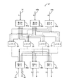
本発明は、一般に、最少量の回路と複雑さを持ち、長レイテンシ命令のデータハザードを効率的に検出する処理システムに関する。本発明の原理をよりよく説明するために、まず図1を参照する。図1は、従来のスーパスカラ処理システム15(以下、単に処理システム15とする)を示す。処理システム15は、コンピュータプログラムの命令を受取り、各命令を複数のパイプライン21のうちの1つに割当てる命令分配ユニット18を含んでいる。各パイプライン21は、そのパイプライン21に割当てられた各命令を、適当であれば処理および実行するよう構成されている。
【0019】
通常、各パイプライン21は、特定のタイプの命令(例えば、整数演算、浮動小数点演算、メモリ演算等)のみを処理するように構成されている。従って、命令分配ユニット18は、各命令をその命令と適合するパイプライン21にのみ割当てるよう構成されている。さらに図1では、簡潔のために、制御回路24と、ハザード検出回路25と、「スコアボード」と呼ばれることが多いレジスタファイル27とが、1つのパイプライン21に結合されているように示されているが、各パイプライン21が同様に制御回路24とハザード検出回路25とスコアボード27と結合されていることに留意するべきである。しかしながら、望ましいならば、長レイテンシ命令を処理しないパイプライン21については、スコアボード27の書込みポートに1つのパイプライン21を結合する接続31を取除いてもよい。
【0020】
処理システム15によって受取られる命令の実行時に、処理システム15に関連する汎用レジスタ29に対しデータの書込みおよび読出しが行われることが多い、ということは周知である。さらに、命令の実行時に汎用レジスタ29が利用される(すなわち、書込みまたは読出しが行われる)場合、通常、命令は汎用レジスタ29を識別するレジスタ識別子を含む。レジスタ識別子は、通常、レジスタ識別子によって識別される汎用レジスタ29に対して一意である、nビットの符号化されたバイナリ値である。
【0021】
ハザード検出回路25は、パイプライン21によって処理されている命令に含まれるレジスタ識別子を受取って比較することにより、RAWおよび/またはWAWデータハザード等のあらゆるデータハザードが、パイプライン21によって処理される命令間に存在するか否かを判断するように構成されている。ハザード検出回路25がデータハザードを検出すると、ハザード検出回路25は、パイプライン21におけるどの命令がデータハザードに関連しているかを示して、制御回路24に対し通知信号を送信する。これに応じて制御回路24は、データハザードに関連するデータエラーを防止するために、1つまたは複数のパイプライン21に制御信号を送信して、その1つまたは複数のパイプライン21をストールさせるようにする(すなわち、一時的に命令の更なる処理を行わないようにする)。データハザードが終了すると、制御回路24はストールされた命令の処理の再開を可能にする。
【0022】
命令の実行には、外部レジスタまたは処理システム15の外部のメモリにおけるロケーションからデータを検索するものもある。かかるデータが処理システム15によって受取られると、処理システム15は通常、データを検索した命令によって識別される汎用レジスタ29に対しデータを書込む。通常、続いてそのデータは後の命令を実行するために利用される。
【0023】
データの検索に必要な時間はデータの位置する場所によって異なり、データの検索を要求する命令は処理システム15によってデータが受取られる前に退避されることが多い。しかしながら、命令が退避されパイプライン21を出てしまうと、ハザード検出回路25は、通常、検索されたデータが少なくとも処理システム15によって受取られるまでは、かかるデータハザードが存在するとしても、パイプライン21にある命令のレジスタ識別子を比較するだけでは、その命令に関連するRAWまたはWAWデータハザードを検出することができなくなる。
【0024】
従って、退避された命令に関連するデータハザードを検出するために、通常、追加のステップがとられる。例えば、図1に示す実施の形態において、退避されかかっているプロデューサにより書込み保留状態がもたらされる場合、プロデューサに含まれかつ書込み保留状態に関連する(すなわち、書込みがなされる汎用レジスタ29を識別する)レジスタ識別子が、1組の接続31を介してスコアボード27に送信される。なお、簡単のために、図1はパイプライン21のうちの1つをスコアボード27に結合する1組の接続31のみを示しているが、一般的に、複数のパイプライン21をスコアボード27の異なる書込みポートにそれぞれ結合する複数組の接続31があることを留意するべきである。長レイテンシ命令を処理する各パイプライン21は、図1において接続31の組がそのパイプライン21のうちの1つをスコアボード27に結合するようにスコアボード27に結合されなければならないが、必要であれば、複数のパイプライン21が同様にスコアボード27に結合されてもよい。
【0025】
スコアボード27は、図2に示すように、複数のレジスタ32(以下、スコアボードレジスタ32とする)を含む。スコアボードレジスタ32の各々は、汎用レジスタ29(図1)のうちの異なる1つにそれぞれ対応し、1ビット値を有する。スコアボード27は、接続31に結合された書込みポート34aを含む。書込みポート34aは、書込み保留状態に関連するプロデューサに含まれる上述したレジスタ識別子を受取り、受取ったレジスタ識別子によって識別される汎用レジスタ29に対応するスコアボードレジスタ32のビット値をアサートする。レジスタ識別子は符号化されていることが多く、従って書込みポート34aは、適当なスコアボードレジスタ32のビットをアサートする前に、レジスタ識別子を復号化する。
【0026】
再び図1を参照すると、書込み保留状態に関連する汎用レジスタ29に書込まれるデータは、通常、汎用レジスタ29を識別するレジスタ識別子と共にインタフェース42によって受取られる。インタフェース42は、上記のデータを識別された汎用レジスタ29に送信し、接続45aを介してレジスタ識別子をスコアボード27に送信する。スコアボード27は、書込みポート34b(図2)を有している。この書込みポート34bは、接続45aに結合されており、接続45aからレジスタ識別子を受取り、レジスタ識別子によって識別される汎用レジスタ29に対応するスコアボードレジスタ32のビット値をデアサートする。
【0027】
インタフェース42は1サイクルで複数のレジスタ識別子を受取る場合があるため、処理システム15は、図1および図2に示すように、インタフェース42によってスコアボード27に受取られたレジスタ識別子の各々をそれぞれ送信しかつ受取るために、接続45b等の複数組の他の接続と、書込みポート34c等の複数の他の書込みポートとを有してもよい。さらにスコアボード27は、通常、種々のパイプライン21からレジスタ識別子を受取るために、それら種々のパイプライン21にそれぞれ結合された複数の書込みポート34aを含む。従って、書込みポート34a、34b、34cの数は非常に大きくなる可能性があり、従って、書込みポート34a、34b、34cをスコアボードレジスタ32とインタフェースする回路は、複雑かつ高価となる可能性がある。
【0028】
上述したように、スコアボードレジスタ32のビット値をアサートおよびデアサートすることにより、ハザード検出回路25は、スコアボード27のスコアボードレジスタ32に含まれるビットに基づいて、退避された命令に関連するデータハザードを検出することができる。すなわち、スコアボードレジスタ32に含まれる、レジスタ29のうちの特定の1つに対応するビットがアサートされている場合、1つの汎用レジスタ29に対する書込み保留状態が存在する。従って、パイプライン21によって処理されている別の命令が1つの汎用レジスタ29からのデータを利用する場合、RAWまたはWAWデータハザードが存在する可能性がある。しかしながら、上記スコアボードレジスタ32に含まれるビットがデアサートされている場合、その時点で、退避された命令による1つの汎用レジスタ29への書込み保留状態はない。従って、1つの汎用レジスタ29に書込む退避された命令に関連するRAWまたはWAWデータハザードは、存在しないはずである。
【0029】
各パイプライン21は、通常、パイプライン21のうちの1つについて図1および図2によって示されているように、1つの読出しポート48aに結合されている。パイプライン21における保留状態の命令と前に退避された命令との間のデータハザードを検出するために、パイプライン21は、通常、接続49を介して、保留状態の命令を実行する際に使用する汎用レジスタ29を識別する符号化したnビットレジスタ識別子を送信する。読出しポート48aは、レジスタ識別子を受取り復号化する。また、読出しポート48aは、レジスタ識別子によって識別される汎用レジスタ29に対応するスコアボードレジスタ32に含まれるビットを分析する。上記スコアボードレジスタ32のビットが、レジスタ識別子によって識別される汎用レジスタ29に対する書込み保留状態があることを示す場合、読出しポート48aは、接続52を介して、先行する命令に関連するデータハザードが存在する可能性があることを示す信号を送信する。例えば、読出しポート48aによって分析されるスコアボードレジスタ32のビットがアサートされている場合、読出しポート48aはアサートされた1ビット信号を送信する。あるいは、読出しポート48aはデアサートされた1ビット信号を送信する。接続52を介して送信された信号に基づいて、ハザード検出回路25は保留状態の命令に関連するデータハザードが存在するか否かを判断する。
【0030】
スコアボード27に対する書込みおよびスコアボード27からの読出しに関連する有限量の遅延があることに留意されたい。従って、ハザード検出回路25に迅速な更新を提供するために、インタフェース42を介してスコアボード27に送信されるレジスタ識別子はまた、バイパス接続54aおよび/または54bを介してスコアボード27をバイパスする。状況によっては、ハザード検出回路25は、バイパス接続54aおよび/または54bからのレジスタ識別子を利用して、パイプライン21のうちの1つにおける命令に対するストールを防止するかまたは取除くことができる。
【0031】
さらに、各命令は、実行時に複数の汎用レジスタ29を利用してもよく、そのため、複数のレジスタ識別子を含んでもよい。別個の組の接続49、52および別個の読出しポート48aは、通常、それぞれ可能性のあるレジスタ識別子について提供される。例えば、システム15の構造が、各パイプライン21における各命令が3つまでのレジスタ識別子を含むことができるようなものである場合、通常、3組の接続49を介して各パイプライン21に結合される少なくとも3つの読出しポート48a、48b、48cがある。従って、当業者は認めるだろうが、システム15における読出しポート48a、48b、48cおよび接続49、52の数は、多くのスーパスカラプロセッサについて非常に多くなる可能性があり、それによって、書込みの量およびシステム15の複雑さが増大する。システム15の複雑さおよびコストを低減するため、およびシステム15における貴重な空間を維持するために、書込みポート34a、34bおよび/または34cと読出しポート48a、48bおよび/または48cとを含むスコアボード27に対する書込みおよびスコアボード27からの読出しに利用される回路を最小限にすることが望ましい。
【0032】
一般に、本発明は、効率的にかつ回路の量と複雑さを最小限にしつつ、退避された命令によってもたらされる書込み保留状態を追跡する処理システムを提供する。図3は、本発明の好ましい実施の形態の原理に従う処理システム50を示す。図3に示すように、処理システム50は、メモリ59に格納されたコンピュータプログラム57からの命令を実行するために、コンピュータシステム55内で採用することができる。
【0033】
処理システム50は、1つまたは複数のバスを含むことができるローカルインタフェース62を介して、コンピュータシステム55内の他の要素と通信しかつそれらを駆動する。さらに、例えばキーボードまたはマウス等の入力装置64を用いて、コンピュータシステム55のユーザからデータを入力することができ、スクリーンディスプレイ66またはプリンタ68を用いて、ユーザにデータを出力することができる。ディスク格納機構71はローカルインタフェース62に接続されて、不揮発性ディスク(例えば、磁気、光等)に対しおよび不揮発性ディスクからデータを転送することができる。コンピュータシステム55は、コンピュータシステム55をネットワーク75とデータを交換することができるようにするネットワークインタフェース73に接続することが可能である。
【0034】
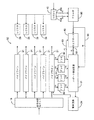
従来のシステム15と同様、図4に示すように、処理システム50は、少なくとも1つのパイプライン21と、制御回路24と、ハザード検出回路81と、スコアボード82と、を含む。図4において、制御回路24およびハザード検出回路81には1つのパイプライン21のみが結合されているが、好ましい実施の形態では、制御回路24およびハザード検出回路81に対し他のパイプライン21が同様に結合されている。さらに図4は、接続83およびデコーダ84を介してスコアボード82に結合された1つのパイプライン21を示す。好ましい実施の形態では、長レイテンシ命令を処理する各パイプライン21が同様にスコアボード82に結合されているが、必要な場合、スコアボード82に対し他のパイプライン21を同様に結合することも可能である。
【0035】
従来のハザード検出回路25と同様に、好ましい実施の形態のハザード検出回路81は、前の命令のレジスタ識別子に基づき、パイプライン21によって処理されている命令に関連するデータハザードを検出する。このため、パイプライン21における各命令のレジスタ識別子はハザード検出回路81に送信され、ハザード検出回路81はレジスタ識別子を比較してデータハザードを検出する。しかしながら、ハザード検出回路81に送信される各nビット符号化レジスタ識別子は、まずデコーダ84によって復号化されてmビットレジスタ識別子となる。ここで、mは、処理システム50が命令の実行によって生成されるデータを読出しおよび書込みするために使用する汎用レジスタ29の数に対応する。
【0036】
ここで、mビット復号化レジスタ識別子の各ビットは、特定の汎用レジスタ29に対応する。デコーダ84は、汎用レジスタ29のうちの1つを識別するnビットレジスタ識別子を受取ると、その1つの汎用レジスタ29に対応するmビットレジスタ識別子におけるビットをアサートし、mビットレジスタ識別子における残りのビットをデアサートするよう構成されている。従って、mビットの復号化レジスタ識別子においていずれのビットがアサートされているかを検出することにより、mビットの復号化レジスタ識別子によりいずれの汎用レジスタ29が識別されているかを判断することができる。「System and Method for Efficiently Detecting Data Hazards Between Instructions of a Computer Program」と題する、本願と同一の譲受人に譲渡された米国特許出願(代理人整理番号第10971185号)と、「System and Method for Utilizing Instruction Attributes to Detect Data Hazards」と題する、本願と同一の譲受人に譲渡された米国特許出願(代理人整理番号第10971333号)とは、参照によりその開示内容が本明細書に援用されたものとするが、デコーダ84を実現するために使用することができる回路構成と、ハザード検出回路81が2つの命令のうちのレジスタ識別子が一致する時、そして2つの命令間にデータハザードが存在する時を検出するために使用することができる回路構成とを詳細に述べている。
【0037】
従来のスコアボード27と同様、図5に示すように、スコアボード82は複数のスコアボードレジスタ32を有し、各スコアボードレジスタ32およびそこに含まれるビット値は、特定の汎用レジスタ29に対応する。スコアボードレジスタ32のビットは、アサートされると、対応する汎用レジスタ29の退避された命令による書込み保留状態があるということを示す。スコアボードレジスタ32のビットは、デアサートされると、かかる書込み保留状態が存在しないということを示す。
【0038】
従って、スコアボード82は、従来からのスコアボード27と同様に、退避された命令によってもたらされる書込み保留状態に、いずれの汎用レジスタ29が関連しているかを示す。しかしながら、上述したように、スコアボード27は一般的に書込みポート34a、34b、34cを介して接続31、45a、45bによって送信されるレジスタ識別子を復号化する。図5に示すように、好ましい実施の形態では、スコアボード82は接続83を介してデコーダ84のうちの少なくとも1つに結合されている。従って、上記デコーダ84は、ハザード検出回路81とスコアボード82との両方に対し、mビットの復号化したレジスタ識別子を提供する。接続83によって送信されるレジスタ識別子がmビットを有しているので、接続83の各々をスコアボードレジスタ32に直接結合することができ、そのため、スコアボード82における書込みポート34a(図2)の必要が無くなる。
【0039】
すなわち、接続83のうちの1つによって送信される各ビットは、そのビットと同じ汎用レジスタ29に対応するスコアボードレジスタ32に提供される。言い換えれば、接続83によって送信されるmビットレジスタ識別子が、汎用レジスタ29のうちの特定の1つを識別する場合、その1つの汎用レジスタ29に対応するスコアボードレジスタ32のみがアサートされたビットを受取るべきであり、他のスコアボードレジスタ32はデアサートされたビットを受取るべきである。その結果、スコアボード82によって受取られたレジスタ識別子によって識別される汎用レジスタ29にどのスコアボードレジスタ32が対応するかを検出するために、スコアボード82に書込みポート34a(図2)を必要としない。代りに、適当なスコアボードレジスタ32に適当なビット値を提供するために、ハザード検出回路81にmビットレジスタ識別子を提供する同じデコーダ84が使用されてもよい。従って、好ましい実施の形態において、データハザードを検出し、かつスコアボード82のビットを適当にアサートするために必要な、回路の量および複雑性が最小化される。
【0040】
さらに、接続45a、45bから受取られるレジスタ識別子は、好ましくは、スコアボード82における書込みポート34b、34c(図2)の代りにデコーダ85によって復号化される。すなわち、デコーダ85は、インタフェース42から現時点で送信されているnビットの符号化レジスタ識別子を受取り、同じサイクルで受取られるnビットのレジスタ識別子によって識別される汎用レジスタ29の各々を識別するmビットの復号化レジスタ識別子を出力するよう、構成されている。
【0041】
好ましい実施の形態では、値mは処理システム50における汎用レジスタ29の数に対応し、デコーダ85によって送信されるmビットの復号化レジスタ識別子の各ビットは、異なる汎用レジスタ29に対応する。デコーダ85は、同じサイクルで受取られたnビットレジスタ識別子のうちの1つによって識別される汎用レジスタ29に対応する、mビットの復号化レジスタ識別子の各ビットをアサートし、かつ、mビットの復号化レジスタ識別子の残りのビットをデアサートするよう、構成されている。従って、復号化レジスタ識別子の対応するビットがアサートされている時、汎用レジスタ29は、デコーダ85によって送信されるmビットの復号化レジスタ識別子によって識別される。
【0042】
スコアボード82は、デコーダ85から新たな復号化レジスタ識別子を受取ると、復号化レジスタ識別子によって識別される汎用レジスタ29に対応するスコアボードレジスタ32におけるビットをデアサートするよう設計されている。これは、上記汎用レジスタ29に対する書込み保留状態が、すでに存在していないはずだからである。
【0043】
すなわち、各スコアボードレジスタ32は、デコーダ85から復号化されたレジスタ識別子のビットを受取る。スコアボードレジスタ32は、好ましくは、スコアボードレジスタ32によって受取られたビットと同じ汎用レジスタ29に対応する。言い換えれば、デコーダ85からの復号化レジスタ識別子が汎用レジスタ29のうちの1つを識別する場合、識別された汎用レジスタ29に対応するスコアボードレジスタ32は、デコーダ85からアサートされたビットを受取らなければならない。さらに、デコーダ85から受取ったビットの値がアサートされている場合、アサートされたビット値を受取るスコアボードレジスタ32は、スコアボードレジスタ32に含まれるビット値をクリアする(例えば、デアサートする)よう設計されている。その結果、汎用レジスタ29のうちの特定の1つに対応するスコアボードレジスタ32のアサートされたビットは、現時点でその1つの汎用レジスタ29に対する書込み保留状態があることを示し、スコアボードレジスタ32のデアサートされたビットは、現時点でかかる書込み保留状態が無いことを示す。
【0044】
望ましい場合、スコアボード82は、ハザード検出回路81がRAWおよびWAWデータハザード等のデータハザードを適切に検出することができるように、スコアボードレジスタ32に含まれるデータに対応する信号を、接続88を介してハザード検出回路81に送信する。好ましい実施の形態では、接続88の各々がスコアボードレジスタ32のうちの異なる1つに結合されており、それによって接続88に結合された1つのスコアボードレジスタ32と同じ汎用レジスタ29に対応する。従って、ハザード検出回路81に送信される信号は、mビットデータワードであり、mビットデータワードの各ビットは、異なるスコアボードレジスタ32からのビット値に対応する。その結果、mビットデータワードにおける各アサートされたビットは、汎用レジスタ29のうちの特定の1つに対する書込み保留状態があることを示す。mビットデータワードは、本質的に、複数の汎用レジスタ29を同時に識別することができるmビットレジスタ識別子である。好ましい実施の形態では、スコアボードレジスタ32の各々が接続88のうちの1つを介してハザード検出回路83に直接結合されているので、従来のスコアボード27における読出しポート48a、48b、48c(図2)を削除することができる。
【0045】
しかしながら、スコアボード27に対する書込みおよびスコアボード27からの読出しにおいて有限量の遅延があるため、スコアボード82によって送信されるデータは、必ずしも更新されるとは限らない。その結果、書込み保留状態が実際に最近終了した場合、接続88を介して送信されるデータワードは書込み保留状態が存在することを示してしまう可能性がある。ハザード検出回路81に対して使用可能な最新の情報を提供するために、従来の処理システム15のバイパス接続54a、54bと同様に、スコアボード82をバイパスするバイパス接続94は、デコーダ85からの復号化mビットレジスタ識別子をハザード検出回路81に提供する。
【0046】
ハザード検出回路81は、パイプライン21からデコーダ84を介して受取るmビットレジスタ識別子を、接続88および/または94から受取るmビットレジスタ識別子と比較して、データハザードを検出する。図6は、パイプライン21から受取ったmビットレジスタ識別子を、接続88または94から受取ったmビットレジスタ識別子と比較することによってデータハザードを検出するために使用することができる、回路101の例示的な実現を示す。
【0047】
各ANDゲート104は、パイプライン21からmビットレジスタ識別子の1ビット、および接続88または94からmビットレジスタ識別子の1ビットを受取る。さらに、同じANDゲート104によって受取られる各ビットは、同じ汎用レジスタ29に対応する。従って、ANDゲート104のうちの1つは、パイプライン21からのmビットレジスタ識別子が、接続88または94からのmビットレジスタ識別子によって識別される汎用レジスタ29のうちの1つを識別する場合にのみ、アサートされた出力を生成しなければならない。その結果、ANDゲート104のうちの1つがアサートされた出力を生成する場合、パイプライン21からのmビットレジスタ識別子に関連する命令は、書込み保留状態下にある汎用レジスタ29を利用し、従って上記の命令に関連するデータハザードが存在する可能性がある。
【0048】
従って、ANDゲート104のうちの1つがアサートされた出力を生成する場合、ハザード検出回路81は、パイプライン21から受取るmビットレジスタ識別子に関連する命令に関連するデータハザードを検出する。一方、ANDゲート104のうちのいずれもアサートされた出力を生成しない場合、パイプライン21から受取ったmビットレジスタ識別子によって識別される汎用レジスタ29に関連する書込み保留状態はないはずである。従って、パイプライン21からのmビットレジスタ識別子に関連する命令によって利用される汎用レジスタ29への書込み保留状態はないはずであり、ハザード検出回路81は、上記の命令に関連するデータハザードを検出しない。
【0049】
上記の方法に従って、ハザード検出回路81は、データハザードを検出しパイプライン21における命令の1つに関連するデータハザードが存在することを示す信号を制御回路24に送信してもよい。これに応じて制御回路24は、検出されたデータハザードからのデータエラーを防止するために、上記の命令がストールされるべきであることを示す制御信号をその命令を処理しているパイプライン21に送信してもよい。これに応じてパイプライン21は、好ましくは命令をストールする。
【0050】
ハザード検出回路81は、上記の命令に関連するmビットレジスタ識別子を、接続88または94から受取るmビットレジスタ識別子と比較することにより、上述したデータハザードがもはや存在しないことを検出してもよい。すなわち、命令によって利用される汎用レジスタ29に書込まれるよう予定されたデータが、処理システム50によって受取られていてもよく、それにより、上述したデータハザードが終了する。ハザード検出回路81により上述した命令に関連するデータハザードが検出されなかったことに応答して、制御回路24は、命令がストールされるべきではないことを示す制御信号を、その命令を処理しているパイプライン21に送信する。これに応答してパイプライン21は、命令に対するストールを取除き、パイプライン21による命令の処理を再開する。
【0051】
なお、デコーダ85は、本発明の必要な特徴ではないことに留意されたい。すなわち、必要ならば、スコアボード82に接続45aおよび/または45bから受取られるレジスタ識別子を復号化するための回路を含めることが可能であり、接続45aおよび/または45bによって送信されるレジスタ識別子は、従来の処理システム15と同様、ハザード検出回路81に対して直接送信されてもよい。かかる実施の形態では、ハザード検出回路81は、必要であれば、接続45aおよび/または45bによって送信されるレジスタ識別子を適切に復号化するためのデコーダを含んでもよい。
【0052】
さらに、簡単のために本明細書では、処理システム15および50が4つの汎用レジスタ29のみを含むものとして示してきた。従って、mの値は、好ましくは、図面に示す実施の形態において4に等しい。しかしながら、他の実施の形態において、処理システム50はいかなる数のレジスタ29を有することも可能であり、従って他の実施の形態では、mの値は他の整数値とすることができる。さらに、レジスタ識別子は、mより大きいかまたは小さい長さのデータワードに復号化または符号化することが可能であるが、かかる実施の形態は、通常、好ましい実施の形態より効率的ではない。すなわち、ハザード検出回路81にmビットレジスタ識別子を提供することにより、処理システム50の回路構成を縮小することができるのみでなく、ハザード検出回路81によるデータハザードの検出を簡略化しおよび/またはより適切に行うことができる。
【0053】
さらに、図5を図2と比較することによって分かるように、好ましい実施の形態の構成は、スコアボード82における読出しポート48a、48b、48cを不要にする。さらに、デコーダ84のうちの1つは、スコアボード82とハザード検出回路81との両方に対して送信されるレジスタ識別子を復号化する機能を効率的に実行することができる。その結果、好ましい実施の形態では、処理システム50の実現に必要な回路の量が最小化され、それにより、処理システム50のコストおよび複雑さが最小化される。
【0054】
動作
処理システム50および関連する方法の好ましい使用および動作を以下に述べる。
【0055】
コンピュータプログラム57(図3)の命令の処理において、処理システム50(図4)は、実行時にメモリ59からデータ(以下、「検索データ」と言う)を検索して処理システム50の汎用レジスタ29に格納する、第1の命令を受取るものとする。また、処理システム50は、後にコンピュータプログラム57から、実行時に検索データを利用する第2の命令を受取るものとする。両命令を実行するために上記汎用レジスタ29が利用されるので、第1の命令および第2の命令は共に、上記汎用レジスタ29を識別するレジスタ識別子を含む。
【0056】
第1の命令および第2の命令がパイプライン21によって同時に処理される間、ハザード検出回路81は、2つの命令の復号化レジスタ識別子を比較することにより、2つの命令間のRAWデータハザードを検出することができる。ある時点で、制御回路24は、RAWデータハザードに関連するエラーを防止するために第2の命令がストールされるようにしてもよい。検索データが処理システム50によって受取られる前に第1の命令が退避された場合、第1の命令が退避されていても、RAWハザードが第1の命令と第2の命令との間に存在する可能性がある。
【0057】
第1の命令が退避された後にハザード検出回路81がRAWハザードを検出することができるようにするために、検索データを受取る汎用レジスタ29を識別するmビットレジスタ識別子は、第1の命令を処理するパイプライン21に結合された接続83を介してスコアボード82に送信される。これに応じて、スコアボード82は、上記レジスタ識別子によって識別される汎用レジスタ29(すなわち、検索データを受取る汎用レジスタ29)に対応するスコアボードレジスタ32(図5)のビットをアサートする。
【0058】
上記スコアボードレジスタ32に含まれるビット値および第2の命令のレジスタ識別子に基づき、ハザード検出回路81は、第1の命令が退避されていても、上述したRAWデータハザードを検出することができる。これに応じて、制御回路24は、第2の命令がストールされるようにしてもよい。
【0059】
検索データがインタフェース42によって受取られると、検索データを受取る汎用レジスタ29を識別するレジスタ識別子が、接続45aまたは45bを介してデコーダ85に送信される。デコーダ85は、レジスタ識別子に応じて、少なくとも上記汎用レジスタ29を識別するmビットの復号化レジスタ識別子を生成する。ここで、上記汎用レジスタ29に対応する、復号化レジスタ識別子のビットがアサートされる。そして、このmビットレジスタ識別子は、スコアボード82に送信され、復号化レジスタ識別子のアサートされたビットに応じて、スコアボード82は上記汎用レジスタ29に対応するスコアボードレジスタ32(図5)のビットをデアサートする。また、スコアボード82に送信されたmビットレジスタ識別子は、バイパス接続94を介してハザード検出回路81に送信される。
【0060】
上述したスコアボードレジスタ32のデアサートされたビット値かまたはバイパス接続94によって送信された上記mビットレジスタ識別子のいずれかに基づいて、ハザード検出回路81はRAWハザードがすでに存在しないことを検出する。これに応じて、制御回路24は第2の命令に対するストールを取除き、上述したRAWデータハザードに関連するデータエラーをもたらすことなく、第2の命令の処理が再開される。
【0061】
本発明は、本明細書において、長レイテンシ命令によって生成されるデータが使用可能でない時を示すためにスコアボード82を利用するものとして説明されたが、あらゆるタイプの命令によって生成されるデータが使用不可能である時を示すために、スコアボード82を同様に使用することもできることに留意されたい。特に、保留状態の命令(すなわち、まだ退避されておらず、パイプライン21によってまだ処理中である命令)によって生成されるデータが使用不可能であるか否かを示すために、スコアボード82を使用することができる。さらに、本発明を、本明細書においていくつかの例において、ロード命令によって生成されたデータが使用不可能であるか否かを示すためにスコアボード82を利用するものとして述べたが、そのように限定されるべきではなく、スコアボード82は、あらゆる他のタイプの命令によって生成されるデータが使用不可能であるか否かを示すために使用することができる。
【0062】
本発明の精神および原理から実質的に逸脱することなく、多くの変形および変更を本発明の上記実施の形態に対して行うことができる。
【0063】
本発明は例として以下の実施形態を含む。
(1) コンピュータプログラム(57)の命令を処理するシステム(50)であって、
複数のレジスタ(32)と、
該レジスタ(32)にそれぞれ対応する複数の接続(88)と、
前記命令の少なくとも1つを処理し実行するよう構成され、該1つの命令が前記レジスタ(32)のうちの1つを識別するレジスタ識別子に関連しているパイプライン(21)と、
前記複数の接続(88)と前記パイプライン(21)とに結合され、前記複数のレジスタ(32)にそれぞれ対応する複数のビットを有し、前記第1のレジスタ識別子を受取り該第1のレジスタ識別子に応じて該1つのレジスタ(32)に対応する該ビットのうちの1つをアサートするよう構成され、少なくとも該1つのレジスタ(32)を識別する第2のレジスタ識別子を受取り該第2のレジスタ識別子に応じて該1ビットをデアサートするよう構成され、さらに、前記接続(88)の1つによって該1ビットを送信するように構成されており、該1ビットが、該1ビットの値に基づいておよび該接続(88)のうちのいずれが該1ビットを送信しているかに基づいて該1つのレジスタ(32)に対する書込み保留状態が存在するか否かを示す、スコアボード(82)と、
前記複数の接続(88)に結合され、前記1ビットを受取ると共に該1ビットに基づいてデータハザードが存在するか否かを検出するよう構成された、ハザード検出回路(81)と、
を含むシステム(50)。
【0064】
(2) 前記スコアボード(82)は前記複数のビットの各々を含むデータワードを前記ハザード検出回路(81)に送信するようさらに構成され、該データワードの各アサートされたビットが、前記レジスタ(32)の異なる1つが書込み保留状態に関連していることを示す、前記(1)に記載のシステム(50)。
【0065】
(3) 前記スコアボード(82)は複数のレジスタ(32)を含み、該レジスタ(32)の各々が前記ビットの異なる1つを含むと共に前記接続(88)の異なる1つに結合されている、前記(1)に記載のシステム(50)。
【0066】
(4) 前記第1のレジスタ識別子は復号化レジスタ識別子であって、
前記命令によって規定された符号化レジスタ識別子を受取るとともに、該符号化レジスタ識別子を復号化して前記復号化レジスタ識別子にするよう構成され、該復号化レジスタ識別子を前記スコアボード(82)に送信するようさらに構成されたデコーダ(84)をさらに含む、前記(1)に記載のシステム(50)。
【0067】
(5) 前記デコーダ(84)は前記復号化レジスタ識別子を前記ハザード検出回路(81)に送信するようさらに構成されている、前記(4)に記載のシステム(50)。
【0068】
(6) 前記復号化レジスタ識別子は複数のビットを含み、前記1つのレジスタ(32)に対応する該復号化レジスタ識別子の該ビットのうちの1つはアサートされ、該復号化レジスタ識別子の残りのビットはデアサートされる、前記(4)に記載のシステム(50)。
【0069】
(7) コンピュータプログラムの命令を処理する方法であって、
複数のレジスタ(32)を提供するステップと、
各々のビットが、該レジスタ(32)の対応する1つが書込み保留状態に関連しているか否かを示す、複数のビットを保持するステップと、
該ビットの各々を含むデータワードを送信し、該データワードの各アサートされたビットが、前記レジスタ(32)の異なる1つが書込み保留状態に関連していることを示すステップと、
前記データワードを受取るステップと、
該データワードに基づいてデータハザードを検出するステップと、
を含む方法。
【0070】
(8) 命令を処理するステップと、
該命令に関連する符号化レジスタ識別子を受取るステップと、
該符号化レジスタ識別子を復号化して復号化レジスタ識別子にするステップと、
該復号化レジスタ識別子を他のレジスタ識別子と比較するステップと、
該比較するステップに基づいてデータハザードを検出するステップと、
前記復号化レジスタ識別子に基づいて前記ビットのうちの1つを変更するステップと、
をさらに含む前記(7)に記載の方法。
【0071】
(9) コンピュータプログラムの命令を処理する方法であって、
複数のレジスタ(32)を提供するステップと、
各々が該レジスタ(32)のうちの1つにそれぞれ対応する複数のビットを保持するステップと、
各々が該レジスタ(32)のうちの1つにそれぞれ対応する複数の接続(88)を提供するステップと、
前記ビットを介して、該レジスタ(32)のいずれが書込み保留状態に関連しているかを示すステップと、
前記接続(88)のうちの特定の1つにより該レジスタ(32)のうちの特定の1つに対応する前記ビットのうちの1つを送信し、該特定の1つの接続(88)が、該特定の1つのレジスタ(32)に対応しているステップと、
該特定の1つの接続(88)によって送信される該1ビットに基づいてデータハザードを検出するステップと、
を含む方法。
【0072】
(10) 命令を処理するステップと、
該命令に関連するレジスタ識別子を受取るステップと、
該レジスタ識別子のビットを前記特定の1つの接続(88)によって送信される前記特定の1ビットと比較するステップと、
該比較するステップに基づいて前記検出するステップを実行するステップと、をさらに含む前記(9)に記載の方法。
【0073】
【発明の効果】
本発明によれば、データハザードを検出するためにスコアボードを利用するシステムを実現するのに必要な回路の量が最小化され、それによりシステムのコストおよび複雑さが最小化される。
【図面の簡単な説明】
【図1】従来の処理システムを示すブロック図である。
【図2】図1に示す処理システムのスコアボードを示すブロック図である。
【図3】本発明による処理システムを採用するコンピュータシステムを示すブロック図である。
【図4】図3に示す処理システムを示すブロック図である。
【図5】図4に示す処理システムのスコアボードを示すブロック図である。
【図6】図4に示すハザード検出回路を実現するために使用することができる回路を示すブロック図である。
【符号の説明】
21 パイプライン
32 スコアボードレジスタ
50 処理システム
57 コンピュータプログラム
81 ハザード検出回路
82 スコアボード
84 デコーダ
88 接続[0001]
BACKGROUND OF THE INVENTION
The present invention relates generally to data processing techniques, and in particular, relates to an instruction by efficiently indicating when data generated by the execution of one instruction is available in the execution of another instruction. The present invention relates to a processing system and method that enables detection of data hazards. The present invention is particularly advantageous when the latency for generating data for one instruction is relatively long.
[0002]
[Prior art]
Pipelining has been developed to improve the performance of many processors. In pipeline processing, the processor includes at least one pipeline that can process multiple instructions simultaneously. Thus, execution of an instruction in a pipeline may begin before the result of execution of a previous instruction in the pipeline becomes available, thereby creating several data hazards.
[0003]
For example, the first instruction may generate data and write the data to a specific register at the time of execution, and the second instruction may use data generated by the first instruction at the time of execution. If the second instruction is executed before the data generated by the first instruction is available, a data error occurs. Thus, there is a data hazard between the two instructions until the data generated by the first instruction is available. This type of data hazard is commonly referred to as a “read after write” (RAW) data hazard.
[0004]
In other situations, when executed, the second instruction may write data to the same register as the first instruction that started executing before the second instruction. If the second instruction generates and writes its data to the register before the first instruction, there is a possibility of a data error. This is because after both instructions are completely executed and processed, the register will have data for the first instruction rather than the second instruction. Therefore, there is a data hazard between the two instructions until the data generated by the first instruction is written to the register. This type of data hazard is commonly referred to as a “write after light” (WAW) data hazard.
[0005]
To prevent errors from the data hazards described above and other types of data hazards, most superscalar processors have a hazard detection circuit that detects data hazards associated with instructions being processed by the processor pipeline. The hazard detection circuit typically detects the data hazard described above by detecting when a subsequent instruction uses (eg, writes or reads) the same register as the previous instruction that has not yet generated usable data. Is detected.
[0006]
However, the data generated by the first instruction is not until the first instruction is completely retired by the pipeline processing the first instruction (for example, the first instruction is pipelined). May not be available for use by other instructions or for writing to certain registers of the processor. For example, a load instruction may generate a request to retrieve data from memory external to the processor when executed. Depending on where the data is in the memory hierarchy, it may take several clock cycles to thousands of clock cycles before returning the data to the processor in response to the above request. Thus, the processor cannot receive the data generated by the first instruction until after the first instruction exits the processor pipeline or is otherwise saved. In other words, the data generated by the first instruction is not available for execution of other instructions until after the first instruction exits the processor pipeline or is otherwise saved. An instruction such as the load instruction described above that generates usable data after the instruction is saved by the pipeline is referred to as a “long latency instruction” in this specification.
[0007]
To facilitate the process of detecting data hazards for long latency instructions, the processor is typically provided with a register file, commonly referred to as a “scoreboard”. This indicates when the processor has not yet received the data generated in response to the previous execution of the producer (ie, the instruction that generates the data). In other words, the scoreboard indicates when there is a pending write to the general register. As used herein, the term “write pending state” means that data generated by a previously executed instruction will be written to a general-purpose register, but is still written to that general-purpose register. Used to represent a situation that is not included. As is well known in the art, a “general purpose register” is one of a set of registers that is written by execution of a write instruction and / or read by execution of a read instruction.
[0008]
The scoreboard has a plurality of registers, each register containing a 1-bit value. Each of the scoreboard registers and the bit values contained therein corresponds to one of the general purpose registers of the processor that receives data generated by execution of the write instruction. If the write instruction is saved before the data generated by the write instruction is written to the general purpose register that should receive the data, the bit value in the scoreboard register corresponding to that general purpose register is asserted. Furthermore, when the data generated by the write instruction is finally written into the general-purpose register, the above bit value is deasserted. Therefore, by analyzing the bit value of the scoreboard register corresponding to one general-purpose register, it can be determined whether there is a write pending state for that general-purpose register.
[0009]
Each asserted bit value in the scoreboard indicates that there is a write pending state to the general register corresponding to the asserted bit value. Therefore, to prevent errors from RAW or WAW data hazards, at least until the write pending state ends (ie, until the data intended to be written to the general register is actually written to that general register). Any instruction being processed by the processor must not write to or read from the general purpose registers described above. Further, each deasserted bit value in the scoreboard indicates that there is currently no write pending state to the general register corresponding to the deasserted bit value. Thus, instructions being processed by the processor can read or write to the general purpose registers described above without generating any errors from the RAW or WAW data hazards.
[0010]
Preventing errors from RAW or WAW data hazards by stalling one or more instructions being processed by the processor if a RAW or WAW data hazard is detected, such as by analyzing a scoreboard Many. U.S. Patent Application No. 09 / 390,199, filed September 7, 1999, entitled `` Superscalar Processing System and Method for Efficiently Performing In Order Processing of Instructions '', is designed to prevent data hazards. Describes the process of stalling instructions in more detail. When an instruction is stalled, the processor temporarily prevents further processing of the instruction until the data hazard causing the stall is complete.
[0011]
[Problems to be solved by the invention]
However, the wiring and other circuitry typically used for writing to and reading from the scoreboard is relatively complex and often utilizes a relatively large amount of surface area within the processor. In order to minimize processor costs, it is desirable to minimize the circuitry required to detect data hazards. In particular, it is desirable to minimize and simplify the circuitry required for writing to and reading from the scoreboard.
[0012]
Thus, there is an open need in the industry for an efficient system and method that utilizes scoreboards to detect data hazards.
[0013]
[Means for Solving the Problems]
The present invention overcomes the deficiencies and deficiencies of the prior art described above. In general, the present invention provides a system and method for executing instructions of a computer program and efficiently indicating the presence of a write pending state in a general purpose register used to execute the instructions.
[0014]
Structurally, the processing system of the present invention utilizes a plurality of general purpose registers, a plurality of connections, a pipeline, a scoreboard, and a hazard detection circuit. Each of the plurality of connections corresponds to a general purpose register. The scoreboard holds a plurality of bits that indicate whether there is a write pending state for the register to which each bit corresponds. The scoreboard uses one bit to indicate whether there is a write pending state for one general register, based on the value of that one bit, and which connection is used to send that one bit Based on whether or not it is transmitted to the hazard detection circuit. The hazard detection circuit detects whether a data hazard exists based on the one bit.
[0015]
According to another feature of the invention, a decoder is used to decode a register identifier associated with data being written to one of the general purpose registers. The decoder sends a register identifier to both the scoreboard and the hazard detection circuit. The hazard detection circuit can detect a data hazard using the register identifier, and the scoreboard can change one of the bits of the scoreboard using the register identifier.
[0016]
The present invention can also be viewed as providing a method for processing instructions of a computer program. The method can be broadly conceptualized by the following steps. A step of providing a plurality of general-purpose registers; a step of holding a plurality of bits each corresponding to one of the general-purpose registers; and a plurality of connections each corresponding to one of the general-purpose registers , Indicating via a bit which general register is associated with a write pending state, and one of the bits corresponding to a particular one of the general purpose registers with a particular one Transmitting over a specific one of the connections corresponding to one general purpose register and detecting a data hazard based on one bit transmitted over the specific one connection.
[0017]
Other features and advantages of the present invention will become apparent to those skilled in the art from the following detailed description. All such features and advantages are intended to be included herein within the scope of the present invention and protected by the following claims.
[0018]
DETAILED DESCRIPTION OF THE INVENTION
The present invention generally relates to a processing system having a minimum amount of circuitry and complexity and efficiently detecting data hazards of long latency instructions. To better explain the principles of the present invention, reference is first made to FIG. FIG. 1 shows a conventional superscalar processing system 15 (hereinafter simply referred to as processing system 15). The
[0019]
Typically, each
[0020]
It is well known that data is often written to and read from general purpose registers 29 associated with the
[0021]
The
[0022]
Some instruction executions retrieve data from an external register or a location in memory external to the
[0023]
The time required for data retrieval depends on where the data is located, and instructions that require data retrieval are often saved before the data is received by the
[0024]
Thus, additional steps are usually taken to detect data hazards associated with saved instructions. For example, in the embodiment shown in FIG. 1, if a write pending state is caused by a producer that is about to be evacuated, the general purpose register 29 included in the producer and associated with the write pending state (ie, the write is made) ) A register identifier is sent to the
[0025]
As shown in FIG. 2, the
[0026]
Referring again to FIG. 1, data written to general purpose register 29 associated with a write pending state is typically received by
[0027]
Since the
[0028]
As described above, by asserting and deasserting the bit value of the
[0029]
Each
[0030]
Note that there is a finite amount of delay associated with writing to and reading from the
[0031]
Further, each instruction may use a plurality of general purpose registers 29 at the time of execution, and thus may include a plurality of register identifiers. A separate set of
[0032]
In general, the present invention provides a processing system that tracks write pending conditions caused by saved instructions while efficiently and minimizing the amount and complexity of circuitry. FIG. 3 illustrates a
[0033]
The
[0034]
Similar to the
[0035]
Similar to the conventional
[0036]
Here, each bit of the m-bit decoding register identifier corresponds to a specific general-
[0037]
Like the
[0038]
Thus, the
[0039]
That is, each bit transmitted by one of the
[0040]
Furthermore, register identifiers received from
[0041]
In the preferred embodiment, the value m corresponds to the number of general purpose registers 29 in the
[0042]
When the
[0043]
That is, each
[0044]
If desired, the
[0045]
However, because there is a finite amount of delay in writing to and reading from the
[0046]
The
[0047]
Each AND
[0048]
Thus, if one of the AND
[0049]
In accordance with the method described above,
[0050]
The
[0051]
It should be noted that the
[0052]
Further, for simplicity,
[0053]
Further, as can be seen by comparing FIG. 5 with FIG. 2, the preferred embodiment configuration eliminates the need for
[0054]
Action
Preferred uses and operations of the
[0055]
In processing instructions of the computer program 57 (FIG. 3), the processing system 50 (FIG. 4) retrieves data (hereinafter referred to as “search data”) from the
[0056]
While the first instruction and the second instruction are processed simultaneously by the
[0057]
The m-bit register identifier identifying the
[0058]
Based on the bit value included in the
[0059]
When search data is received by the
[0060]
Based on either the deasserted bit value of the
[0061]
Although the present invention has been described herein as utilizing the
[0062]
Many variations and modifications may be made to the above-described embodiments of the invention without departing substantially from the spirit and principles of the invention.
[0063]
The present invention includes the following embodiments as examples.
(1) A system (50) for processing instructions of a computer program (57),
Multiple registers (32),
A plurality of connections (88) each corresponding to the register (32);
A pipeline (21) configured to process and execute at least one of said instructions, said one instruction being associated with a register identifier identifying one of said registers (32);
A plurality of bits coupled to the plurality of connections (88) and the pipeline (21), each of which corresponds to the plurality of registers (32), and receives the first register identifier; Responsive to an identifier configured to assert one of the bits corresponding to the one register (32), receiving a second register identifier identifying at least the one register (32), and the second Configured to deassert the 1 bit in response to a register identifier, and further configured to transmit the 1 bit over one of the connections (88), wherein the 1 bit is set to the value of the 1 bit. And a scoreboard (82) indicating whether there is a write pending state for the one register (32) based on which of the connections (88) is transmitting the one bit And,
A hazard detection circuit (81) coupled to the plurality of connections (88) and configured to receive the one bit and detect whether a data hazard exists based on the one bit;
Including system (50).
[0064]
(2) The scoreboard (82) is further configured to transmit a data word including each of the plurality of bits to the hazard detection circuit (81), wherein each asserted bit of the data word is stored in the register ( 32. The system (50) of (1) above, indicating that a different one of 32) is associated with a write pending state.
[0065]
(3) The scoreboard (82) includes a plurality of registers (32), each of the registers (32) including a different one of the bits and coupled to a different one of the connections (88). The system (50) according to (1) above.
[0066]
(4) The first register identifier is a decryption register identifier,
Receiving an encoded register identifier defined by the instruction, configured to decode the encoded register identifier into the decoded register identifier, and transmit the decoded register identifier to the scoreboard (82); The system (50) of (1), further comprising a configured decoder (84).
[0067]
(5) The system (50) according to (4), wherein the decoder (84) is further configured to transmit the decoding register identifier to the hazard detection circuit (81).
[0068]
(6) The decoding register identifier includes a plurality of bits, one of the bits of the decoding register identifier corresponding to the one register (32) is asserted, and the remaining of the decoding register identifier The system (50) of (4) above, wherein the bit is deasserted.
[0069]
(7) A method of processing instructions of a computer program,
Providing a plurality of registers (32);
Holding a plurality of bits, each bit indicating whether a corresponding one of the registers (32) is associated with a write pending state;
Transmitting a data word including each of the bits, each asserted bit of the data word indicating that a different one of the registers (32) is associated with a write pending state;
Receiving the data word;
Detecting a data hazard based on the data word;
Including methods.
[0070]
(8) processing the instruction;
Receiving an encoded register identifier associated with the instruction;
Decoding the encoded register identifier into a decoded register identifier;
Comparing the decrypted register identifier with other register identifiers;
Detecting a data hazard based on the comparing step;
Changing one of the bits based on the decoding register identifier;
The method according to (7), further comprising:
[0071]
(9) A method of processing instructions of a computer program,
Providing a plurality of registers (32);
Holding a plurality of bits, each corresponding to one of the registers (32);
Providing a plurality of connections (88) each corresponding to one of the registers (32);
Via the bit indicating which of the registers (32) is associated with a write pending state;
Transmitting one of the bits corresponding to a particular one of the registers (32) by a particular one of the connections (88), the particular one connection (88) being A step corresponding to the one particular register (32);
Detecting a data hazard based on the one bit transmitted by the particular one connection (88);
Including methods.
[0072]
(10) processing the instruction;
Receiving a register identifier associated with the instruction;
Comparing the bit of the register identifier with the particular one bit transmitted by the particular one connection (88);
The method according to (9), further comprising: performing the detecting step based on the comparing step.
[0073]
【The invention's effect】
In accordance with the present invention, the amount of circuitry required to implement a system that utilizes a scoreboard to detect data hazards is minimized, thereby minimizing system cost and complexity.
[Brief description of the drawings]
FIG. 1 is a block diagram showing a conventional processing system.
FIG. 2 is a block diagram showing a score board of the processing system shown in FIG.
FIG. 3 is a block diagram illustrating a computer system employing a processing system according to the present invention.
4 is a block diagram showing the processing system shown in FIG. 3. FIG.
FIG. 5 is a block diagram showing a score board of the processing system shown in FIG. 4;
6 is a block diagram showing a circuit that can be used to implement the hazard detection circuit shown in FIG. 4;
[Explanation of symbols]
21 Pipeline
32 Scoreboard register
50 treatment system
57 Computer program
81 Hazard detection circuit
82 Scoreboard
84 Decoder
88 connections
Claims (3)
複数のレジスタと、
該レジスタにそれぞれ対応する複数の接続と、
前記命令を処理し実行するよう構成された少なくとも1つのパイプラインと、
前記複数の接続と前記少なくとも1つのパイプラインとに結合され、前記複数のレジスタにそれぞれ対応する複数のビットを有し、前記複数のレジスタの1つに対する書込み保留状態が存在するか否かを示す、前記ビットの各々を、前記複数の接続の異なるものを介して送信するスコアボードと、
前記命令の少なくとも1つに関連した、少なくとも1つの符号化レジスタ識別子を、前記複数のレジスタにそれぞれ対応する複数のビットを有し、前記複数のレジスタの少なくとも1つを識別する復号化レジスタ識別子へ復号化するように構成された復号回路と、
前記複数の接続の各々に結合され、前記送信されたビットの各々を、前記復号化レジスタ識別子のビットのそれぞれと比較し、前記送信されたビットの、前記復号化レジスタ識別子のビットとの比較に基づいてデータハザードを検出するよう構成された、ハザード検出回路と、を含み、
前記復号回路は、前記少なくとも1つのパイプラインから前記符号化レジスタ識別子を受け取り、復号化レジスタ識別子へ復号化するように構成され、さらに、復号化レジスタ識別子をハザード検出回路とスコアボードへ送信するように構成されたデコーダを含むコンピュータ・システム。A computer system for processing instructions of a computer program,
Multiple registers,
A plurality of connections each corresponding to the register;
At least one pipeline configured to process and execute the instructions;
Coupled to the plurality of connections and the at least one pipeline, each having a plurality of bits corresponding to the plurality of registers, indicating whether a write pending state exists for one of the plurality of registers; A scoreboard that transmits each of the bits over a different one of the plurality of connections;
At least one encoded register identifier associated with at least one of the instructions to a decoded register identifier having a plurality of bits each corresponding to the plurality of registers and identifying at least one of the plurality of registers A decoding circuit configured to decode;
Coupled to each of the plurality of connections, comparing each of the transmitted bits with each of the bits of the decoding register identifier, and comparing the transmitted bits with the bits of the decoding register identifier A hazard detection circuit configured to detect a data hazard based on the
The decoding circuit is configured to receive the encoding register identifier from the at least one pipeline and decode it into a decoding register identifier, and further transmit the decoding register identifier to the hazard detection circuit and the scoreboard. A computer system comprising a decoder configured in
少なくとも1つのパイプラインと、
複数のレジスタと、
該レジスタの異なるものに各々が対応する複数の接続と、
複数のビットを保持し、該ビットを介して複数のレジスタのうちのどれが書込み保留状態に関連しているかを示す手段であって、複数のビットを複数の接続を介して送信するように構成され、複数の接続の各々により送信される各々のビットは、各々の接続に対応するレジスタが、書込み保留状態に関連しているかを示す手段と、
前記複数のビットと、前記少なくとも1つのパイプラインに現在存在する少なくとも1つの命令に関連する、復号化レジスタ識別子との比較を実行するように構成され、さらに、該比較に基づいて少なくとも1つのデータハザードを検出するよう構成された、ハザード検出回路と、
前記少なくとも1つのパイプラインから、前記少なくとも1つの命令に関連した符号化レジスタ識別子を受け取り、該符号化レジスタ識別子を、複数のレジスタの少なくとも1つを識別する、復号化レジスタ識別子へ復号化する手段であって、復号化レジスタ識別子を前記ハザード検出回路と前記保持手段へ送信するように構成された手段とを含むシステム。A system for processing instructions of a computer program,
At least one pipeline,
Multiple registers,
A plurality of connections each corresponding to a different one of the registers;
Means for holding a plurality of bits and indicating which of the plurality of registers are associated with a write pending state via the bits and configured to transmit the plurality of bits over a plurality of connections Each bit transmitted by each of the plurality of connections means for indicating whether a register corresponding to each connection is associated with a write pending state;
Configured to perform a comparison of the plurality of bits with a decoding register identifier associated with at least one instruction currently present in the at least one pipeline, and further comprising at least one data based on the comparison A hazard detection circuit configured to detect a hazard;
Means for receiving an encoded register identifier associated with the at least one instruction from the at least one pipeline and decoding the encoded register identifier into a decoded register identifier that identifies at least one of a plurality of registers; A system comprising: a decryption register identifier; and means configured to transmit the hazard detection circuit to the holding means.
命令を少なくとも1つのパイプラインを介して処理するステップと、
複数のレジスタを提供するステップと、
各々が該レジスタのうちの1つにそれぞれ対応する複数のビットを、スコアボード内に保持するステップと、
各々が該レジスタのうちの1つにそれぞれ対応する複数の接続を提供するステップと、
前記ビットを介して、該レジスタのいずれが書込み保留状態に関連しているかを示すステップと、
前記複数の接続の異なるものを介して前記ビットの各々を、スコアボードから送信するステップと、
前記命令の少なくとも1つに関連した、少なくとも1つのレジスタ識別子を、前記複数のレジスタにそれぞれ対応する複数のビットを有し、前記複数のレジスタの少なくとも1つを識別する復号化レジスタ識別子へ、デコーダを介して復号化するステップと
前記送信されたビットの各々を、前記復号化レジスタ識別子のビットのそれぞれと比較するステップと、
該比較に基づいてデータハザードを検出するステップと、
前記復号化レジスタ識別子に基づいて、前記スコアボードビットのうちの1つを変更するステップと、
前記少なくとも1つのレジスタ識別子を、前記少なくとも1つのパイプラインから前記デコーダへ送信するステップと、
前記復号化レジスタ識別子を、前記デコーダから前記スコアボードへ送信するステップと、を含む方法。A method for processing instructions of a computer program comprising:
Processing instructions through at least one pipeline;
Providing a plurality of registers;
Holding a plurality of bits in the scoreboard, each corresponding to a respective one of the registers;
Providing a plurality of connections, each corresponding to one of the registers;
Via the bit, indicating which of the registers are associated with a write pending state;
Transmitting each of the bits from the scoreboard via different ones of the plurality of connections;
A decoder for decoding at least one register identifier associated with at least one of the instructions into a decoding register identifier having a plurality of bits each corresponding to the plurality of registers and identifying at least one of the plurality of registers; Deciphering via: and comparing each of the transmitted bits with each of the bits of the decoding register identifier;
Detecting a data hazard based on the comparison;
Changing one of the scoreboard bits based on the decoding register identifier;
Transmitting the at least one register identifier from the at least one pipeline to the decoder;
Transmitting the decoding register identifier from the decoder to the scoreboard.
Applications Claiming Priority (2)
| Application Number | Priority Date | Filing Date | Title |
|---|---|---|---|
| US09/490,392 US6643762B1 (en) | 2000-01-24 | 2000-01-24 | Processing system and method utilizing a scoreboard to detect data hazards between instructions of computer programs |
| US09/490392 | 2000-01-24 |
Publications (3)
| Publication Number | Publication Date |
|---|---|
| JP2001209537A JP2001209537A (en) | 2001-08-03 |
| JP2001209537A5 JP2001209537A5 (en) | 2005-06-02 |
| JP3756409B2 true JP3756409B2 (en) | 2006-03-15 |
Family
ID=23947846
Family Applications (1)
| Application Number | Title | Priority Date | Filing Date |
|---|---|---|---|
| JP2001002038A Expired - Fee Related JP3756409B2 (en) | 2000-01-24 | 2001-01-10 | Data hazard detection system |
Country Status (2)
| Country | Link |
|---|---|
| US (2) | US6643762B1 (en) |
| JP (1) | JP3756409B2 (en) |
Families Citing this family (15)
| Publication number | Priority date | Publication date | Assignee | Title |
|---|---|---|---|---|
| US7373484B1 (en) * | 2004-01-12 | 2008-05-13 | Advanced Micro Devices, Inc. | Controlling writes to non-renamed register space in an out-of-order execution microprocessor |
| US7487337B2 (en) * | 2004-09-30 | 2009-02-03 | Intel Corporation | Back-end renaming in a continual flow processor pipeline |
| US7698536B2 (en) * | 2005-08-10 | 2010-04-13 | Qualcomm Incorporated | Method and system for providing an energy efficient register file |
| US7370176B2 (en) * | 2005-08-16 | 2008-05-06 | International Business Machines Corporation | System and method for high frequency stall design |
| US20090055636A1 (en) * | 2007-08-22 | 2009-02-26 | Heisig Stephen J | Method for generating and applying a model to predict hardware performance hazards in a machine instruction sequence |
| US9311085B2 (en) * | 2007-12-30 | 2016-04-12 | Intel Corporation | Compiler assisted low power and high performance load handling based on load types |
| TW201101177A (en) * | 2009-06-23 | 2011-01-01 | Rdc Semiconductor Co Ltd | Microprocessor and data write-in method thereof |
| US9529596B2 (en) | 2011-07-01 | 2016-12-27 | Intel Corporation | Method and apparatus for scheduling instructions in a multi-strand out of order processor with instruction synchronization bits and scoreboard bits |
| US9858077B2 (en) * | 2012-06-05 | 2018-01-02 | Qualcomm Incorporated | Issuing instructions to execution pipelines based on register-associated preferences, and related instruction processing circuits, processor systems, methods, and computer-readable media |
| JP6024281B2 (en) * | 2012-08-21 | 2016-11-16 | 富士通株式会社 | Processor |
| CN103235716B (en) * | 2013-04-19 | 2016-03-02 | 中国科学院自动化研究所 | A kind of for detecting the relevant device of pipeline data |
| US11175924B2 (en) | 2017-10-06 | 2021-11-16 | International Business Machines Corporation | Load-store unit with partitioned reorder queues with single cam port |
| US10606591B2 (en) | 2017-10-06 | 2020-03-31 | International Business Machines Corporation | Handling effective address synonyms in a load-store unit that operates without address translation |
| US10417002B2 (en) | 2017-10-06 | 2019-09-17 | International Business Machines Corporation | Hazard detection of out-of-order execution of load and store instructions in processors without using real addresses |
| EP4276625A3 (en) * | 2018-01-29 | 2024-01-24 | Micron Technology, Inc. | Memory controller |
Family Cites Families (14)
| Publication number | Priority date | Publication date | Assignee | Title |
|---|---|---|---|---|
| US4903196A (en) * | 1986-05-02 | 1990-02-20 | International Business Machines Corporation | Method and apparatus for guaranteeing the logical integrity of data in the general purpose registers of a complex multi-execution unit uniprocessor |
| US4891753A (en) * | 1986-11-26 | 1990-01-02 | Intel Corporation | Register scorboarding on a microprocessor chip |
| DE69311330T2 (en) * | 1992-03-31 | 1997-09-25 | Seiko Epson Corp | COMMAND SEQUENCE PLANNING FROM A RISC SUPER SCALAR PROCESSOR |
| US5630149A (en) * | 1993-10-18 | 1997-05-13 | Cyrix Corporation | Pipelined processor with register renaming hardware to accommodate multiple size registers |
| US6108769A (en) * | 1996-05-17 | 2000-08-22 | Advanced Micro Devices, Inc. | Dependency table for reducing dependency checking hardware |
| US5860017A (en) | 1996-06-28 | 1999-01-12 | Intel Corporation | Processor and method for speculatively executing instructions from multiple instruction streams indicated by a branch instruction |
| US5859999A (en) | 1996-10-03 | 1999-01-12 | Idea Corporation | System for restoring predicate registers via a mask having at least a single bit corresponding to a plurality of registers |
| US5784588A (en) * | 1997-06-20 | 1998-07-21 | Sun Microsystems, Inc. | Dependency checking apparatus employing a scoreboard for a pair of register sets having different precisions |
| US6272520B1 (en) * | 1997-12-31 | 2001-08-07 | Intel Corporation | Method for detecting thread switch events |
| US6266766B1 (en) * | 1998-04-03 | 2001-07-24 | Intel Corporation | Method and apparatus for increasing throughput when accessing registers by using multi-bit scoreboarding with a bypass control unit |
| EP1004959B1 (en) * | 1998-10-06 | 2018-08-08 | Texas Instruments Incorporated | Processor with pipeline protection |
| US6550001B1 (en) * | 1998-10-30 | 2003-04-15 | Intel Corporation | Method and implementation of statistical detection of read after write and write after write hazards |
| US6219781B1 (en) * | 1998-12-30 | 2001-04-17 | Intel Corporation | Method and apparatus for performing register hazard detection |
| US6304955B1 (en) * | 1998-12-30 | 2001-10-16 | Intel Corporation | Method and apparatus for performing latency based hazard detection |
-
2000
- 2000-01-24 US US09/490,392 patent/US6643762B1/en not_active Expired - Lifetime
-
2001
- 2001-01-10 JP JP2001002038A patent/JP3756409B2/en not_active Expired - Fee Related
-
2003
- 2003-08-07 US US10/636,073 patent/US7146490B2/en not_active Expired - Fee Related
Also Published As
| Publication number | Publication date |
|---|---|
| US20040030867A1 (en) | 2004-02-12 |
| JP2001209537A (en) | 2001-08-03 |
| US6643762B1 (en) | 2003-11-04 |
| US7146490B2 (en) | 2006-12-05 |
Similar Documents
| Publication | Publication Date | Title |
|---|---|---|
| JP4829541B2 (en) | Digital data processing apparatus with multi-level register file | |
| JP3561915B2 (en) | System and method for assigning tags to control instruction processing in a superscalar processor | |
| US6493820B2 (en) | Processor having multiple program counters and trace buffers outside an execution pipeline | |
| EP0380859B1 (en) | Method of preprocessing multiple instructions | |
| US6115808A (en) | Method and apparatus for performing predicate hazard detection | |
| JP3756409B2 (en) | Data hazard detection system | |
| US20080082755A1 (en) | Administering An Access Conflict In A Computer Memory Cache | |
| US20060206693A1 (en) | Method and apparatus to execute an instruction with a semi-fast operation in a staggered ALU | |
| JP3631146B2 (en) | System for detecting data hazards | |
| JP2001092660A (en) | System and method for processing super scaler for efficiently preventing error generated caused by write- after-write data hazard | |
| US7373486B2 (en) | Partially decoded register renamer | |
| US9588770B2 (en) | Dynamic rename based register reconfiguration of a vector register file | |
| US6715060B1 (en) | Utilizing a scoreboard with multi-bit registers to indicate a progression status of an instruction that retrieves data | |
| KR101466934B1 (en) | Distributed dispatch with concurrent, out-of-order dispatch | |
| JP3704046B2 (en) | System and method for fusing data used to detect data hazards | |
| JP3756410B2 (en) | System that provides predicate data | |
| US5848256A (en) | Method and apparatus for address disambiguation using address component identifiers | |
| JP3756411B2 (en) | System for detecting data hazards | |
| US6829700B2 (en) | Circuit and method for supporting misaligned accesses in the presence of speculative load instructions | |
| US7457932B2 (en) | Load mechanism | |
| US20020124163A1 (en) | System and method for supporting precise exceptions in a data processor having a clustered architecture |
Legal Events
| Date | Code | Title | Description |
|---|---|---|---|
| A521 | Request for written amendment filed |
Free format text: JAPANESE INTERMEDIATE CODE: A523 Effective date: 20040810 |
|
| A621 | Written request for application examination |
Free format text: JAPANESE INTERMEDIATE CODE: A621 Effective date: 20040810 |
|
| A977 | Report on retrieval |
Free format text: JAPANESE INTERMEDIATE CODE: A971007 Effective date: 20051209 |
|
| TRDD | Decision of grant or rejection written | ||
| A01 | Written decision to grant a patent or to grant a registration (utility model) |
Free format text: JAPANESE INTERMEDIATE CODE: A01 Effective date: 20051220 |
|
| A61 | First payment of annual fees (during grant procedure) |
Free format text: JAPANESE INTERMEDIATE CODE: A61 Effective date: 20051221 |
|
| R150 | Certificate of patent or registration of utility model |
Free format text: JAPANESE INTERMEDIATE CODE: R150 |
|
| LAPS | Cancellation because of no payment of annual fees |