JP3698139B2 - ELECTRO-OPTICAL DEVICE WITH MOUNTING CASE, PROJECTION TYPE DISPLAY DEVICE, AND MOUNTING CASE - Google Patents
ELECTRO-OPTICAL DEVICE WITH MOUNTING CASE, PROJECTION TYPE DISPLAY DEVICE, AND MOUNTING CASE Download PDFInfo
- Publication number
- JP3698139B2 JP3698139B2 JP2002370075A JP2002370075A JP3698139B2 JP 3698139 B2 JP3698139 B2 JP 3698139B2 JP 2002370075 A JP2002370075 A JP 2002370075A JP 2002370075 A JP2002370075 A JP 2002370075A JP 3698139 B2 JP3698139 B2 JP 3698139B2
- Authority
- JP
- Japan
- Prior art keywords
- electro
- optical device
- fins
- mounting case
- cover
- Prior art date
- Legal status (The legal status is an assumption and is not a legal conclusion. Google has not performed a legal analysis and makes no representation as to the accuracy of the status listed.)
- Expired - Fee Related
Links
Images


Classifications
-
- G—PHYSICS
- G02—OPTICS
- G02F—OPTICAL DEVICES OR ARRANGEMENTS FOR THE CONTROL OF LIGHT BY MODIFICATION OF THE OPTICAL PROPERTIES OF THE MEDIA OF THE ELEMENTS INVOLVED THEREIN; NON-LINEAR OPTICS; FREQUENCY-CHANGING OF LIGHT; OPTICAL LOGIC ELEMENTS; OPTICAL ANALOGUE/DIGITAL CONVERTERS
- G02F1/00—Devices or arrangements for the control of the intensity, colour, phase, polarisation or direction of light arriving from an independent light source, e.g. switching, gating or modulating; Non-linear optics
- G02F1/01—Devices or arrangements for the control of the intensity, colour, phase, polarisation or direction of light arriving from an independent light source, e.g. switching, gating or modulating; Non-linear optics for the control of the intensity, phase, polarisation or colour
- G02F1/13—Devices or arrangements for the control of the intensity, colour, phase, polarisation or direction of light arriving from an independent light source, e.g. switching, gating or modulating; Non-linear optics for the control of the intensity, phase, polarisation or colour based on liquid crystals, e.g. single liquid crystal display cells
- G02F1/133—Constructional arrangements; Operation of liquid crystal cells; Circuit arrangements
- G02F1/1333—Constructional arrangements; Manufacturing methods
- G02F1/133308—Support structures for LCD panels, e.g. frames or bezels
-
- G—PHYSICS
- G02—OPTICS
- G02F—OPTICAL DEVICES OR ARRANGEMENTS FOR THE CONTROL OF LIGHT BY MODIFICATION OF THE OPTICAL PROPERTIES OF THE MEDIA OF THE ELEMENTS INVOLVED THEREIN; NON-LINEAR OPTICS; FREQUENCY-CHANGING OF LIGHT; OPTICAL LOGIC ELEMENTS; OPTICAL ANALOGUE/DIGITAL CONVERTERS
- G02F1/00—Devices or arrangements for the control of the intensity, colour, phase, polarisation or direction of light arriving from an independent light source, e.g. switching, gating or modulating; Non-linear optics
- G02F1/01—Devices or arrangements for the control of the intensity, colour, phase, polarisation or direction of light arriving from an independent light source, e.g. switching, gating or modulating; Non-linear optics for the control of the intensity, phase, polarisation or colour
- G02F1/13—Devices or arrangements for the control of the intensity, colour, phase, polarisation or direction of light arriving from an independent light source, e.g. switching, gating or modulating; Non-linear optics for the control of the intensity, phase, polarisation or colour based on liquid crystals, e.g. single liquid crystal display cells
-
- H—ELECTRICITY
- H04—ELECTRIC COMMUNICATION TECHNIQUE
- H04N—PICTORIAL COMMUNICATION, e.g. TELEVISION
- H04N9/00—Details of colour television systems
- H04N9/12—Picture reproducers
- H04N9/31—Projection devices for colour picture display, e.g. using electronic spatial light modulators [ESLM]
- H04N9/3141—Constructional details thereof
- H04N9/3144—Cooling systems
-
- G—PHYSICS
- G02—OPTICS
- G02F—OPTICAL DEVICES OR ARRANGEMENTS FOR THE CONTROL OF LIGHT BY MODIFICATION OF THE OPTICAL PROPERTIES OF THE MEDIA OF THE ELEMENTS INVOLVED THEREIN; NON-LINEAR OPTICS; FREQUENCY-CHANGING OF LIGHT; OPTICAL LOGIC ELEMENTS; OPTICAL ANALOGUE/DIGITAL CONVERTERS
- G02F1/00—Devices or arrangements for the control of the intensity, colour, phase, polarisation or direction of light arriving from an independent light source, e.g. switching, gating or modulating; Non-linear optics
- G02F1/01—Devices or arrangements for the control of the intensity, colour, phase, polarisation or direction of light arriving from an independent light source, e.g. switching, gating or modulating; Non-linear optics for the control of the intensity, phase, polarisation or colour
- G02F1/13—Devices or arrangements for the control of the intensity, colour, phase, polarisation or direction of light arriving from an independent light source, e.g. switching, gating or modulating; Non-linear optics for the control of the intensity, phase, polarisation or colour based on liquid crystals, e.g. single liquid crystal display cells
- G02F1/133—Constructional arrangements; Operation of liquid crystal cells; Circuit arrangements
- G02F1/1333—Constructional arrangements; Manufacturing methods
- G02F1/133382—Heating or cooling of liquid crystal cells other than for activation, e.g. circuits or arrangements for temperature control, stabilisation or uniform distribution over the cell
- G02F1/133385—Heating or cooling of liquid crystal cells other than for activation, e.g. circuits or arrangements for temperature control, stabilisation or uniform distribution over the cell with cooling means, e.g. fans
-
- G—PHYSICS
- G02—OPTICS
- G02F—OPTICAL DEVICES OR ARRANGEMENTS FOR THE CONTROL OF LIGHT BY MODIFICATION OF THE OPTICAL PROPERTIES OF THE MEDIA OF THE ELEMENTS INVOLVED THEREIN; NON-LINEAR OPTICS; FREQUENCY-CHANGING OF LIGHT; OPTICAL LOGIC ELEMENTS; OPTICAL ANALOGUE/DIGITAL CONVERTERS
- G02F2201/00—Constructional arrangements not provided for in groups G02F1/00 - G02F7/00
- G02F2201/36—Airflow channels, e.g. constructional arrangements facilitating the flow of air
Description
【0001】
【発明の属する技術分野】
本発明は、液晶プロジェクタ等の投射型表示装置にライトバルブとして用いられる液晶パネル等の電気光学装置を実装するための実装ケース、また該実装ケースに当該電気光学装置が実装或いは収容されてなる実装ケース入り電気光学装置、及びこのような実装ケース入り電気光学装置を備えてなる投射型表示装置の技術分野に属する。
【0002】
【背景技術】
一般に、液晶パネルを液晶プロジェクタにおけるライトバルブとして用いる場合、該液晶パネルは、液晶プロジェクタを構成する筐体等にいわば裸の状態で設置されるのではなく、該液晶パネルを適当な実装ケースに実装ないし収容した上で、この実装ケース入り液晶パネルを、前記筐体等に設置することが行われる。これは、当該実装ケースに適当なねじ孔等を設けておくことで、液晶パネルの前記筐体等に対する固着を容易に実施することなどが可能となるからである。
【0003】
このような液晶プロジェクタでは、光源から発せられた光源光は、当該実装ケース入り液晶パネルに対して集光された状態で投射されることになる。そして、液晶パネルを透過した光は、スクリーン上に拡大投射されて画像の表示が行われることになる。このように液晶プロジェクタにおいては、拡大投射が一般に予定されているため、前記光源光としては、例えばメタルハライドランプ等の光源から発せられる比較的強力な光が使用されることになる。
【0004】
すると、まず、実装ケース入り液晶パネル、とりわけ液晶パネルの温度上昇が問題となる。すなわち、このような温度上昇が生じると、液晶パネル内において一対の透明基板間に挟持されている液晶の温度も上昇して、該液晶の特性劣化を招く。また特に光源光にむらがあった場合には、部分的に液晶パネルが加熱されて所謂ホットスポットが発生して、液晶の透過率のムラができて投射画像の画質が劣化する。
【0005】
このような液晶パネルの昇温を防止する技術としては、例えば特許文献1等に開示されているものが知られている。この特許文献1では、液晶パネル及び該液晶パネルを収容保持するとともに放熱板が備えられたパッケージ(本明細書にいう「実装ケース」に該当する。)からなる液晶表示モジュールにおいて、前記液晶パネル及び前記放熱板間に放熱シートを設けることにより、液晶パネルの昇温を防止する技術が開示されている。
【0006】
また、このような問題点に対処するため、その他にも、液晶パネルの光入射側に位置する基板に遮光膜を設けること、液晶パネルを実装あるいは収納してなる実装ケースを光反射性材料から構成すること等といった技術も知られている。
【0007】
【特許文献1】
再表WO98/36313
【0008】
【発明が解決しようとする課題】
しかしながら、従来における液晶パネルの昇温防止対策には次のような問題点がある。すなわち、光源光からの強力な光が投射される限り、液晶パネルの温度上昇の問題は常に顕在化するおそれがあるから、更なる高画質化等を図るためには、上記各種の対策に代えて又は加えて、より効率的な温度上昇の防止対策が要求されているという点である。
【0009】
例えば、前記の特許文献1で開示されている放熱シートを利用する対策では、たしかに液晶パネルに蓄積されていく熱を外部へと有効に放射することが可能になるとは考えられるものの、この特許文献1では、放熱「板」或いは放熱「シート」というように、或いは特許文献1のFig2等に示されているように、該放熱シートは、基板全面を覆うようにして設けられることが前提とされているようであるから、反射型の液晶パネルには利用できても、透過型の液晶パネルに対しては無力である。
【0010】
また、遮光膜及び実装ケースによる光反射対策では、それらの面積を増大させれば反射光量が増大するから、たしかに液晶パネルの温度上昇の防止を相応に達成することができると考えられるものの、反射光量をむやみ増大させると、実装ケース入り液晶パネルを収納するハウジング内の迷光を増加させることとなって、画像の品質に悪影響を及ぼすことが考えられる。また、遮光膜については、その面積を広げれば広げるほど、液晶パネルに本来入射・透過されるべき光源光の量が減ることになるから、画像が暗くなってしまうことが考えられる。これでは、より明るい画像を表示しようとして、強力な光源光を用いているという趣旨に反することになる。このように、上記の対策は、抜本的に問題を解決するものとはいえない点にも問題がある。
【0011】
本発明は、上記問題点に鑑みてなされたものであり、比較的強力な投射光が入射される電気光学装置における温度上昇を効率的に抑制可能とする、実装ケース入り電気光学装置及びこれを備えてなる投射型表示装置を提供することを課題とする。また、本発明は、このような実装ケース入り電気光学装置に使用されて好適な実装ケースを提供することをも課題とする。
【0012】
【課題を解決するための手段】
本発明の実装ケース入り電気光学装置は、上記課題を解決するため、画像表示領域に光源から光が入射される電気光学装置と、該電気光学装置の一面に対向するように配置されるプレートと、前記プレートとで前記電気光学装置を収容するカバーとからなり、前記電気光学装置における前記画像表示領域の周辺に位置する周辺領域の少なくとも一部を前記プレート及び前記カバーの少なくとも一方で保持して当該電気光学装置を収納する実装ケースとを備えた実装ケース入り電気光学装置であって、前記カバーは、その表面積を増大させる表面積増大手段を備えている。さらに具体的には、前記プレートは、前記電気光学装置の側面に対向する折り曲げ部を備え、前記カバーは、前記カバーの内側面が前記プレートの前記折り曲げ部に接するとともに、前記カバーの外表面には表面積増大手段として複数のフィンを備えている。
また、本発明の実装ケース入り電気光学装置は、画像表示領域に光源から光が入射される電気光学装置と、
該電気光学装置の一面に対向するように配置されるプレートと、前記プレートとで前記電気光学装置を収容するカバーとからなり、前記電気光学装置における前記画像表示領域の周辺に位置する周辺領域の少なくとも一部を前記プレートで保持するように当該電気光学装置を収納する実装ケースとを備えた実装ケース入り電気光学装置であって、
前記プレートは、前記電気光学装置の側面に対向する折り曲げ部を備え、
前記カバーは、前記電気光学装置の側面に対向する側壁部を有し、前記側壁部の内側面が前記プレートの前記折り曲げ部に接するとともに、前記側壁部の外表面には前記折り曲げ部に対向する位置に複数のフィンを備えていることを特徴とする。
【0013】
本発明の実装ケース入り電気光学装置によれば、画像表示領域に光源から光が入射される電気光学装置が、カバー及びプレートからなる実装ケース内に実装される。このような電気光学装置としては、例えば投射型表示装置におけるライトバルブとして実装される液晶装置或いは液晶パネルが挙げられる。なお、このような実装ケースには、電気光学装置の周辺領域を少なくとも部分的に覆うことにより、当該周辺領域における光抜けを防止したり或いは周辺領域から画像表示領域内に迷光が進入するのを防止する遮光機能を持たせてもよい。
【0014】
そして、本発明では特に、前記カバーは、その表面積を増大させる表面積増大手段を備えている。これにより、カバーの放熱能力を高めることができ、もって電気光学装置の効果的な冷却を実現することができる。これは以下の事情による。
【0015】
まず、電気光学装置には前記光が入射されることにより、該電気光学装置の温度は上昇する。すると、この電気光学装置の熱は、前記周辺領域を保持するプレート及びカバーの少なくとも一方に直接的に伝達され、或いはプレートに伝達された熱は前記当接する部分を介してカバーに間接的に伝達されることになる。この場合、これらプレート及びカバーは、電気光学装置に対するヒートシンクとして機能しているということができる。ここで、本発明においては、カバーには表面積増大手段が備えられていることにより、該カバーの放熱能力、或いは冷却能力は高められている。したがって、カバーは、殆ど常に、好適に冷却された状態にされているということができる。このことは、該カバーが、前述のヒートシンクとしてよりよく機能するということを意味する。
【0016】
以上の結果、本発明によれば、電気光学装置の効果的な冷却が実現されることになるのである。したがって、本発明では、電気光学装置の温度上昇によって発生する不具合(例えば、該電気光学装置を構成し得る液晶層の特性劣化、或いは該液晶層中におけるホットスポットの発生等)を被らなくて済むから、より高品質な画像を表示することが可能となる。
【0017】
本発明の実装ケース入り電気光学装置の一態様では、前記カバーは、前記電気光学装置の側面に対向する側壁部を有し、前記表面積増大手段は、前記側壁部の表面積を増大させる。
【0018】
この態様によれば、表面積増大手段によって、カバーの表面積が増大されるのは、前記側壁部ということになる。ここで、側壁部とは、上述のように電気光学装置の側面に対向する部分であることから、カバー全体において占める割合は、そもそも当初より大きいということができる。本態様では、このようなカバー全体の中で比較的広範な面積を有している側壁部において、前記表面積増大手段が備えられていることにより、カバー全体の面積増大効果をより効果的に享受できることになる。
【0019】
したがって、本態様によれば、前述したようなカバーの放熱能力をより効果的に向上させ、もって電気光学装置の冷却効果をより効果的に享受することができることになる。
【0020】
本発明の実装ケース入り電気光学装置の他の態様では、前記表面積増大手段は、前記カバーの表面に突出するように形成されたフィンを含む。
【0021】
この態様によれば、比較的容易にカバーの表面積を増大させることができる。
【0022】
なお、本態様にいう「フィン」は、カバー本体を形成するのに併せて又はその後に、例えば切削加工、鍛造加工、プレス加工、射出成形又は鋳造等により形成することが可能である。
【0023】
本発明の実装ケース入り電気光学装置の他の態様では、前記フィンは、当該実装ケース入り電気光学装置に対して送られてくる冷却風の流れに沿うようにして形成されている。
【0024】
この態様によれば、フィンは、実装ケース入り電気光学装置に対して送られてくる冷却風の流れに沿うようにして形成されているから、当該フィンに起因するカバーの冷却効果を効果的に引き出すことができる。
【0025】
すなわち仮に、フィンが冷却風の流れを阻害するように形成されているとすると、当該冷却風は、それ以降の部分に流れることが困難となるため、カバーの冷却を効果的に行うことができなくなる。しかし、フィンが冷却風の流れに沿うようにして形成されていれば、当該フィンが冷却風の流れをストップするということがなく、カバー全体に冷却風を行き渡らせることが可能である。これにより、本態様によればカバーの冷却を効果的に行うことができるのである。
【0026】
なお、本態様の「フィンは、冷却風に沿うようにして形成されている」とは、具体的には次のような各場合を含む。例えば第一に、冷却風がカバー周囲を直線的に流れているという場合には、フィンが、当該方向に一致するように形成されているという場合を含む。第二に、冷却風がカバー周囲を渦巻くように流れているという場合においては、当該フィンのカバー上の設置場所に応じて、当該フィンが、その方向を変じて形成されているなどという場合を含む。その他、実装ケース入り電気光学装置を中心として、冷却風がやや不規則な流れをみせる場合においても、当該フィンのカバー上の設置場所に応じて、当該フィンが、前記不規則な流れの方向の全部又は一部に一致するように、その方向を変じて形成されているなどという場合も含む。
【0027】
本発明の実装ケース入り電気光学装置の他の態様では、前記フィンは、直線状に形成されている。
【0028】
この態様によれば、直線状に突出したフィンにより、カバーの表面積を増大することができる。したがって、本態様によれば、カバーの放熱能力を向上させることができる。
【0029】
本発明の実装ケース入り電気光学装置の他の態様では、前記フィンは、千鳥足状に配列されるように形成されている
この態様においては、一般に、「フィン」は複数の小フィン(後述も参照)からなるとともに、これら複数の小フィンが、千鳥足状に配列されるように(より具体的には、「当該小フィンが二列間で交互に配置されるように」、或いは「平面視して市松模様を形成するように」等)形成されているという場合が典型的には想定される。このような態様によれば、千鳥足状に突出したフィンにより、カバーの表面積を増大することができる。したがって、本態様によれば、カバーの放熱能力を向上させることができる。
【0030】
この態様では、前記千鳥足状に配列されるように形成されたフィンは、複数の小フィンが列状に配列されて構成される第1列のフィンと、これに平行に延在し且つ複数の小フィンが列状に配列されて構成される第2列のフィンとを含み、前記第2列のフィンを構成する前記小フィンの少なくとも一つは、前記第1列のフィンを構成し且つ相隣接する前記小フィン間の間隙の位置に対応するように形成されているように構成してもよい。
【0031】
このような構成によれば、前述の千鳥足状に配列されるように形成された「フィン」の配置態様が、より具体的に限定されている。すなわち、本態様では、前記の第1列のフィンを構成する小フィンと、第2列のフィンを構成する小フィンとが、いわば相互に重ならないように且つ互い違いに形成されるようになっている。例えば、第1列のフィンを構成する小フィンに、順番に1(1)、1(2)、…、1(n)という番号を付し、第2列のフィンを構成する小フィンにも、同様に2(1)、2(2)、…、2(n)という番号を付すとすると、1(m)番と1(m+1)番(但し、m=1,2,…,n−1)の小フィン間には、同一列(第1列)に属する小フィンは存在しないが、列を変えた第2列には2(m)番の小フィンが存在するなどという配置態様が採られることになる。
【0032】
これによれば、前記の小フィンが適度な密度でもって配列されることにより、カバーの放熱能力を更に向上させることが可能である。例えば、前述の番号を用いて、仮に、2(m)番の小フィンが、1(m)番の小フィンの隣に存在するような場合を仮定すると、この場合には、これら2(m)番及び1(m)番の小フィンが互いに熱を放散することよって、その周囲(特に、両小フィン間の空気)の温度が上昇し、該両小フィンにおける熱の放散がされにくくなるなどという事態が考えられる。しかるに、本態様によれば、少なくとも、2(m)番の小フィンの「隣」に1(m)番の小フィンが存在するなどということはないから、前述のような不具合を被らなくて済むのである。
【0033】
なお、本態様の表現に代えて、「第1列のフィンを構成する前記小フィンの一つは、前記第2列のフィンを構成し且つ相隣接する前記小フィン間の間隙の位置に対応するように形成されている」というように言い換えても同じである。
【0034】
また、本態様では、あたかも第1列のフィン及び第2列のフィンしか存在しないようであるが、場合によって、二列のフィンに加えて、三列目、四列目、…のフィンが備えられていてよい。このような場合、本態様にいう「第1列のフィン」と「第2列のフィン」との関係は、普遍的に適用され得る。例えば、全部で3列のフィンが形成されているとして、そのうちの1番目の列のフィンと2番目の列のフィンとが、それぞれ、本態様の「第1列のフィン」と「第2列のフィン」との関係を満たし、2番目の列のフィンと3番目の列のフィンとが、それぞれ、本態様の「第2列のフィン」と「第1列のフィン」との関係を満たしているというようである。
【0035】
このような構成では、前記小フィン間の間隙は、前記小フィンの長さよりも大きいように構成してもよい。
【0036】
このような構成によれば、前述のように第2列のフィンを構成する小フィンの一つを、「第1列のフィンを構成する小フィン間の間隙の位置に対応するように形成」すると、当該小フィンの一つを、いわば前記間隙内に完全に収めるように形成することができる。
【0037】
したがって、前述したような小フィンにおける放熱性の向上をより確実に享受することができる。というのも、本構成によれば、2(m)番の小フィンと1(m)番の小フィンとが、隣り合わないことは勿論、前者の一部が後者の一部に「重なり合う」ということもないから、各小フィンにおける放熱作用は、如何なく発揮されることになるからである。
【0038】
また、本構成によれば特に、前記の千鳥足状に配列されるフィンの成形を比較的容易に行うことができる。例えば、本態様にかかるフィンは、以下に述べるような射出成形法等で好適に形成することができる。すなわち、山部及び谷部が交互に形成されたジグザグの型を二つ用意し、一方の型の山部(又は谷部)が他方の型の谷部(又は山部)に噛み合うように、且つ、山型のてっぺんと谷型の底との間に所定の隙間が形成されるように、これら二つの型を配置した後、前記の隙間を用いて射出注入を実施すれば、前述のような配置態様を有する、千鳥足状に配列・形成されたフィンを容易に作ることができる。この場合特に、前記の製造方法において必然的に必要となる型抜きは、極めて容易に行われることになる(前記の二つの型を互いに離間させるように移動させればよい。)。
【0039】
なお、本態様にいう「小フィンの長さ」とは、上の説明からも明らかなように、当該小フィンにおける前記第1列又は前記第2列の列方向に沿った長さのことを言う。
【0040】
或いは、前記小フィン間の間隙を含む前記小フィン間のピッチは3mm以上とされているように構成してもよい。
【0041】
このような構成によれば、小フィン間のピッチが好適に設定されていることにより、前述した当該フィンの形成容易性、或いは放熱性の向上という作用効果を、より効果的に享受することができる。
【0042】
或いは更に、前記小フィンの高さは0.5mm以上、幅は0.3mm以上とされているように構成してもよい。
【0043】
このような構成によれば、小フィンの大きさが好適に設定されることにより、カバーの表面積増大量が十分に確保される。したがって、カバーの放熱能力を有効に向上させることができる。
【0044】
なお、本態様にいう「小フィンの高さ」とは、「カバーの表面に突出」したフィンの先端部から、カバーの表面に至るまでの長さを意味し、「幅」とは、当該小フィンにおける前記第1列又は前記第2列の列方向に交差する方向に沿った長さをいう。
【0045】
本発明の実装ケース入り電気光学装置の他の態様では、前記フィンは、第1列のフィンと、これに平行に延在する第2列のフィンとを含み、前記第1列のフィンと前記第2列のフィンとの間の間隔は1mm以上とされている。
【0046】
この態様によれば、前記フィンは、第1列のフィンと第2列のフィンからなる。この場合、ここにいう「第1列のフィン」及び「第2列のフィン」とは、それぞれ、フィンが千鳥足状に配列されるように形成される場合においては、既に述べたような「第1列のフィン」及び「第2列のフィン」がそのまま該当すると考えることができる。また、この他、フィンが直線状に形成される場合においては、「第1列のフィン」としての直線状のフィンと、「第2列のフィン」としての直線状のフィンとが二列形成されているなどという場合を考えることができる。
【0047】
そして、本態様においては、このような二列のフィンの間隔が1mm以上とされている。これにより、当該実装ケース入り電気光学装置に対して冷却風が送り込まれる場合等においては、その冷却風を前記二列のフィン間にも無理なく行き届かせることが可能となる。
【0048】
特に、投射型表示装置内に本発明に係る実装ケース入り電気光学装置を装着する場合を想定すると、該投射型表示装置に別途設置される冷却ファンと当該実装ケース入り電気光学装置とは、通常、他の構成要素を配置等しなけれならない関係から、相当程度距離を離して設置しなければならなかったり、両者間の位置関係を完全に対向させるように配置することが困難な場合が想定される。このような場合、実装ケース入り電気光学装置には、静圧が低く、風量が小さい冷却風しか送られてこないことが考えられることになる。
【0049】
ここで本態様においては、前述のように二列のフィン間の距離が、1mm以上と比較的大きく設定されていることから、これら二列のフィン間にも、前述のような静圧が低く風量が小さい冷却風を吹きぬかせることが可能となる。そして、これによれば、冷却風に曝されることになるフィンの表面積が増大することになるから、当該フィンの放熱性は更に向上することになる。
【0050】
したがって、本態様によれば、カバー全体の放熱能力を更に向上させることができる。
【0051】
本発明の実装ケース入り電気光学装置の他の態様では、前記表面積増大手段は、前記カバーの表面に窪みをつけるように形成されたディンプルを含む。
【0052】
この態様によれば、比較的容易にカバーの表面積を増大させることができる。
【0053】
なお、本態様にいう「ディンプル」と前記の「フィン」との相違点は、「カバーの表面」を基準面として突出しているか、或いは凹んでいるかということにある。
【0054】
或いは、場合により、本態様にいう「ディンプル」は、「当該実装ケース入り電気光学装置に対して送られてくる冷却風の流れを全く阻害しない」という属性を有していてもよい。この観点からすると、前記のフィンは、前記冷却風の流れを全く阻害しないということはない、という属性を有するものと解した上で、この点について、ディンプル及びフィン間の相違点を設定するという考え方を採ることも可能である。
【0055】
また、本態様にいう「窪みをつけるように」とは、当該ディンプルをカバーの表面に形成する場合において、実際に「窪みをつける」ような加工を実施しなければならないということを意味しない。当該ディンプルの形成方法としては、前記のフィンと同様、カバー本体を形成するのに併せて又はその後に、例えば切削加工、鍛造加工、プレス加工、射出成形又は鋳造等により形成することが可能である。
【0056】
本発明の実装ケース入り電気光学装置の他の態様では、前記カバーは、高熱伝導率材料から構成されている。
【0057】
この態様によれば、カバーが高熱伝導率材料からなるから、前記のフィン、或いはディンプル等の表面積増大手段に起因する作用効果とも相俟って、カバーの放熱能力をより高めることができる。
【0058】
なお、本態様にいう「高熱導電率材料」とは、具体的には例えば、アルミニウム、マグネシウム、銅又はこれらそれぞれの合金等を好適には挙げることができる。
【0059】
本発明の実装ケースは、上記課題を解決するために、画像表示領域に光源から光が入射される電気光学装置の一面に対向するように配置されるプレートと、前記電気光学装置を覆い前記プレートと当接する部分を有するカバーとからなり、前記電気光学装置における前記画像表示領域の周辺に位置する周辺領域の少なくとも一部を前記プレート及び前記カバーの少なくとも一方で保持して当該電気光学装置を収納する実装ケースであって、前記カバーは、その表面積を増大させる表面積増大手段を備えている。
【0060】
本発明の実装ケースによれば、前述の本発明の実装ケース入り電気光学装置に使用されて好適な実装ケースを提供することができる。
【0061】
本発明の実装ケースの一態様では、前記カバーは、前記電気光学装置の側面に対向する側壁部を有し、前記表面積増大手段は、前記側壁部の表面積を増大させる。
【0062】
この態様によれば、前述の本発明の実装ケース入り電気光学装置において、カバーが側壁部を有し、表面積増大手段が、この側壁部の表面積を増大させる態様に使用されて好適な実装ケースを提供することができる。
【0063】
本発明の投射型表示装置は、上記課題を解決するために、前述の本発明の実装ケース入り電気光学装置(但し、その各種態様を含む)と、前記光源と、前記投射光を前記電気光学装置に導く光学系と、前記電気光学装置から出射される投射光を投射する投射光学系と、前記実装ケース入り電気光学装置に対して冷却風を送出する冷却風送出手段とを備えている。
【0064】
本発明の投射型表示装置によれば、前述の本発明の実装ケース入り電気光学装置を具備してなるから、当該実装ケースを構成するカバーの表面積が増大していることにより、また、当該投射型表示装置には前記冷却風送出手段が設けられていることにより、電気光学装置の効果的な冷却を実現することができるから、より高品質な画像を表示することが可能である。
【0065】
本発明のこのような作用及び他の利得は次に説明する実施の形態から明らかにされる。
【0066】
【発明の実施の形態】
以下、本発明の実施の形態を図面に基づいて説明する。
【0067】
(投射型液晶装置の実施形態)
まず、図1を参照して、本発明による投射型液晶装置の実施形態について、その光学ユニットに組み込まれている光学系を中心に説明する。本実施形態の投射型表示装置は、実装ケース入りの電気光学装置の一例たる液晶ライトバルブが3枚用いられてなる複板式カラープロジェクタとして構築されている。
【0068】
図1において、本実施形態における複板式カラープロジェクタの一例たる、液晶プロジェクタ1100は、駆動回路がTFTアレイ基板上に搭載された電気光学装置を含む液晶ライトバルブを3個用意し、夫々RGB用のライトバルブ100R、100G及び100Bとして用いたプロジェクタとして構成されている。液晶プロジェクタ1100では、メタルハライドランプ等の白色光源のランプユニット1102から投射光が発せられると、3枚のミラー1106及び2枚のダイクロイックミラー1108によって、RGBの3原色に対応する光成分R、G及びBに分けられ、各色に対応するライトバルブ100R、100G及び100Bに夫々導かれる。この際特にB光は、長い光路による光損失を防ぐために、入射レンズ1122、リレーレンズ1123及び出射レンズ1124からなるリレーレンズ系1121を介して導かれる。そして、ライトバルブ100R、100G及び100Bにより夫々変調された3原色に対応する光成分は、ダイクロイックプリズム1112により再度合成された後、投射レンズ1114を介してスクリーン1120にカラー画像として投射される。
【0069】
本実施形態のライトバルブ100R、100G及び100Bとしては、例えば、後述の如きTFTをスイッチング素子として用いたアクティブマトリクス駆動方式の液晶装置が使用される。また、当該ライトバルブ100R、100G及び100Bは、後に詳述するように実装ケース入り電気光学装置として構成されている。
【0070】
また、この液晶プロジェクタ1100には、図1に示すように、ライトバルブ100R、100G及び100Bに冷却風を送るためのシロッコファン1300(本発明にいう「冷却風送出手段」の一例に該当する。)が設けられている。このシロッコファン1300は、その側面に複数のブレード1301を備えた略円筒形状の部材を含んでおり、該円筒形状の部材がその軸を中心として回転することで前記ブレード1301が風を生じさせるようになっている。なお、このような原理から、シロッコファン1300で作り出される風は、図1に示されるように、らせん状に渦巻いたものとなる。
【0071】
このような風は、図1において図示されない風路を通じて各ライトバルブ100R、100G及び100Bに送給され、各ライトバルブ100R、100G及び100Bの近傍に設けられた吹き出し口100RW、100GW及び100BWから、これらライトバルブ100R、100G及び100Bに対して送り出されるようになっている。
【0072】
ちなみに、前述したようなシロッコファン1300を用いれば、静圧が高くライトバルブ100R、100G及び100B周囲の狭い空間にも風を送りやすいという利点が得られる。
【0073】
以上説明した構成においては、強力な光源たるランプユニット1102からの投射光により各ライトバルブ100R、100G及び100Bで温度が上昇する。この際、過度に温度が上昇してしまうと、各ライトバルブ100R、100G、100Bを構成する液晶が劣化したり、光源光のむらによる部分的な液晶パネルの加熱によるホットスポットの出現により透過率にムラが生じたりする。そこで、本実施形態では特に、各ライトバルブ100R、100G、100Bは、後述のように、電気光学装置を冷却する能力を有する実装ケースを備えている。このため、後述の如く各ライトバルブ100R、100G、100Bの温度上昇は効率的に抑制されている。
【0074】
なお、本実施形態では好ましくは、液晶プロジェクタ1100のハウジング内には、各ライトバルブ100R、100G、100Bの周辺空間に、冷却媒体を流す循環装置等からなる冷却手段を備える。これにより、後述の如き放熱作用を持つ実装ケース入りの電気光学装置からの放熱を一層効率的に行うことができる。
【0075】
(電気光学装置の実施形態)
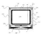
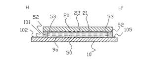
次に本発明の電気光学装置に係る実施形態の全体構成について、図2及び図3を参照して説明する。ここでは、電気光学装置の一例である駆動回路内蔵型のTFTアクティブマトリクス駆動方式の液晶装置を例にとる。本実施形態に係る電気光学装置は、上述した液晶プロジェクタ1100における液晶ライトバルブ100R、100G、100Bとして使用されるものである。ここに、図2は、TFTアレイ基板をその上に形成された各構成要素と共に対向基板の側から見た電気光学装置の平面図であり、図3は、図2のH−H’断面図である。
【0076】
図2及び図3において、本実施形態に係る電気光学装置では、TFTアレイ基板10と対向基板20とが対向配置されている。TFTアレイ基板10と対向基板20との間に液晶層50が封入されており、TFTアレイ基板10と対向基板20とは、画像表示領域10aの周囲に位置するシール領域に設けられたシール材52により相互に接着されている。
【0077】
シール材52は、両基板を貼り合わせるための、例えば紫外線硬化樹脂、熱硬化樹脂等からなり、製造プロセスにおいてTFTアレイ基板10上に塗布された後、紫外線照射、加熱等により硬化させられたものである。また、シール材52中には、TFTアレイ基板10と対向基板20との間隔(基板間ギャップ)を所定値とするためのグラスファイバ或いはガラスビーズ等のギャップ材が散布されている。即ち、本実施形態の電気光学装置は、プロジェクタのライトバルブ用として小型で拡大表示を行うのに適している。
【0078】
シール材52が配置されたシール領域の内側に並行して、画像表示領域10aの額縁領域を規定する遮光性の額縁遮光膜53が、対向基板20側に設けられている。但し、このような額縁遮光膜53の一部又は全部は、TFTアレイ基板10側に内蔵遮光膜として設けられてもよい。
【0079】
画像表示領域の周辺に広がる領域のうち、シール材52が配置されたシール領域の外側に位置する周辺領域には、データ線駆動回路101及び外部回路接続端子102がTFTアレイ基板10の一辺に沿って設けられており、走査線駆動回路104が、この一辺に隣接する2辺に沿って設けられている。更にTFTアレイ基板10の残る一辺には、画像表示領域10aの両側に設けられた走査線駆動回路104間をつなぐための複数の配線105が設けられている。また図2に示すように、対向基板20の4つのコーナー部には、両基板間の上下導通端子として機能する上下導通材106が配置されている。他方、TFTアレイ基板10にはこれらのコーナーに対向する領域において上下導通端子が設けられている。これらにより、TFTアレイ基板10と対向基板20との間で電気的な導通をとることができる。
【0080】
図3において、TFTアレイ基板10上には、画素スイッチング用のTFTや走査線、データ線等の配線が形成された後の画素電極9a上に、配向膜が形成されている。他方、対向基板20上には、対向電極21の他、格子状又はストライプ状の遮光膜23、更には最上層部分に配向膜が形成されている。また、液晶層50は、例えば一種又は数種類のネマティック液晶を混合した液晶からなり、これら一対の配向膜間で、所定の配向状態をとる。
【0081】
尚、図2及び図3に示したTFTアレイ基板10上には、これらのデータ線駆動回路101、走査線駆動回路104等に加えて、画像信号線上の画像信号をサンプリングしてデータ線に供給するサンプリング回路、複数のデータ線に所定電圧レベルのプリチャージ信号を画像信号に先行して各々供給するプリチャージ回路、製造途中や出荷時の当該電気光学装置の品質、欠陥等を検査するための検査回路等を形成してもよい。
【0082】
このように構成された電気光学装置の場合、その動作時には、図3の上側から強力な投射光が照射される。すると、対向基板20、液晶層50、TFTアレイ基板10等における光吸収による発熱によって、当該電気光学装置の温度が上昇する。このような温度上昇は、液晶層50等の劣化を早めると共に、表示画像の品位を劣化させる。
【0083】
そこで、本実施形態では特に、以下に説明する実装ケース入り電気光学装置によって、このような温度上昇を効率的に抑制している。
【0084】
(実装ケース入り電気光学装置―第1実施形態―)
次に、図4から図14を参照して、本発明の第1実施形態に係る実装ケース入り電気光学装置について説明する。
【0085】
ここではまず、図4から図14を参照して、第1実施形態に係る実装ケースの基本構成について説明する。ここに、図4は第1実施形態に係る実装ケースを、前述した電気光学装置とともに示す分解斜視図であり、図5は当該実装ケース入りの電気光学装置の正面図、図6は図5のX1−X1´断面図、図7は図5のY1−Y1´断面図であり、図8は図5のZ1方向から臨んだ後面図である。なお、図4から図8は、電気光学装置を内部に収容した状態における実装ケースを夫々示している。また、図9は当該実装ケースを構成するプレート部の正面図、図10は図9のZ2方向から臨んだ後面図であり、図11は図9のZ3方向から臨んだ側面図である。さらに、図12は当該実装ケースを構成するカバー部の正面図、図13は図12のZ4方向から臨んだ後面図であり、図14は図12のZ5方向から臨んだ側面図である。
【0086】
図4から図8に示すように、実装ケース601は、プレート部610とカバー部620とを備える。実装ケース601内に収容される電気光学装置500は、図2及び図3に示した電気光学装置に加えて、その表面に重ねられた反射防止板等の他の光学要素とを備えてなり、更にその外部回路接続端子にフレキシブルコネクタ501が接続されてなる。尚、偏光板や位相差板は、液晶プロジェクタ1100の光学系に備えるようにしても良いし、電気光学装置500の表面に重ねてもよい。
【0087】
また、TFTアレイ基板10及び対向基板20それぞれの液晶層50に対向しない側には、防塵用基板400が設けられている(図4、図6及び図7参照)。この防塵用基板400は、所定の厚さを有するよう構成されている。これにより、電気光学装置500の周囲に漂うゴミや埃等が、該電気光学装置の表面に直接に付着することが防止される。したがって、拡大投射された画像上に、これらゴミや埃の像が結ばれるという不具合を有効に解消することができる。これは、防塵用基板400が所定の厚さを有することで、光源光の焦点ないしその近傍が、該ゴミや埃が存在する位置(すなわち、防塵用基板400表面)からは外れることによる(デフォーカス作用)。
【0088】
このようにTFTアレイ基板10及び対向基板20並びに防塵用基板400等を備えた電気光学装置500は、図4等に示すように、プレート部610及びカバー部620からなる実装ケース601内に収容されているが、これら電気光学装置500及び実装ケース601間には、図6及び図7に示すように、モールド材630が装填されている。このモールド材630によって、電気光学装置500及び実装ケース601間の接着が確実に行われるとともに、前者の後者の内部における位置ずれの発生が極力防止される。
【0089】
なお、第1実施形態においては、カバー部620の側から光が入射し、電気光学装置500を透過して、プレート部610の側から出射するということを前提とする。つまり、図1でいえば、ダイクロイックプリズム1112に対向するのは、カバー部620ではなくて、プレート部610ということになる。
【0090】
さて、以下では実装ケース601を構成するプレート部610及びカバー部620の構成についてのより詳細な説明を行う。
【0091】
まず第一に、プレート部610は、図4から図11に示すように、平面視して略四辺形状を有する板状の部材であって、電気光学装置500の一面に対向するように配置される。第1実施形態では、プレート部610と電気光学装置500とは相互に直接に当接し、後者が前者に載置されるが如き状態が採られる。
【0092】
より詳細には、プレート部610は、窓部615、強度補強部614、折り曲げ部613、カバー部固定孔612、並びに取付孔611a乃至611d及び611eを有する。
【0093】
窓部615は、略四辺形状を有する部材の一部が開口形状に形成されており、例えば図6中、上方から下方への光の透過を可能とする部分である。電気光学装置500を透過してきた光の出射は、この窓部615によって可能となる。なお、これにより、プレート部610上に電気光学装置500を載置した場合には、該電気光学装置500における画像表示領域10aの周辺に位置する周辺領域が、窓部615の辺縁に当接されるが如き状態になる。プレート部610は、このようにして電気光学装置500の保持を実現する。
【0094】
強度補強部614は、略四辺形状を有する部材の一部を、他の部分の平面からみて盛り上げるような加工を施すことによって形成されており、立体的な形状を有する部分である。これにより、該プレート部614の強度は補強されることになる。なお、該強度補強部614は、電気光学装置500の一辺に略接するが如き位置に形成するとよい(図7参照。ただし、図7では、両者は厳密には接していない。)。
【0095】
折り曲げ部613は、略四辺形状を有する部材の対向する二辺それぞれの一部が、該四辺形状の内側に向かって折り曲げられている部分である。この折り曲げ部613の外側面は、プレート部610及びカバー部620の組み付け時、該カバー部620の内側面に接するようにされている(図6参照)。また、該折り曲げ部613の内側面は、モールド材630を介して電気光学装置500の外側面に接するようにされている(同じく図6参照)。これにより、プレート部610上における電気光学装置500のある程度の位置決めが実現されることになる。
【0096】
加えて、折り曲げ部613の内側面が、モールド材630を介して電気光学装置500の外側面に接するようにされていることは、後者から前者への熱の吸い上げを可能とする。すなわち、プレート部610を、電気光学装置500に対するヒートシンクとして機能させることが可能となる。これによれば、ランプユニット1102による電気光学装置500に対する強力な光照射によって、該電気光学装置500における熱の蓄積の生じることを有効に防止することができる。また、該折り曲げ部613の外側面は、前述のようにカバー部620の内側面に接していることから、前者から後者への熱の伝達も実現されることになる。このように、電気光学装置500からの熱の奪取は、原理的には、プレート部610及びカバー部620の双方において観念される熱容量の分だけ行い得るから、当該電気光学装置500の冷却は、極めて有効に行われることになる。
【0097】
カバー部固定孔612は、カバー部620において対応する位置に形成された凸部621と嵌合するための孔部である。プレート部610及びカバー部620とは、このカバー部固定孔612及び凸部621が互いに嵌合することによって相互に固定される。なお、第1実施形態においては、該カバー部固定孔612は、各図に示すように、二つの孔部からなる(以下、これらの区別が必要な場合には、カバー部固定孔612a及び612bと呼ぶことがある。)。また、これに対応するように、前記凸部621もまた、二つの凸部からなる(以下、これらの区別が必要な場合には、凸部621a及び621bと呼ぶことがある。)。
【0098】
取付孔611a乃至611dは、当該実装ケース入り電気光学装置を、図1に示した如き液晶プロジェクタ1100内に取り付けする際に利用される。第1実施形態においては、該取付孔611a乃至611dは、略四辺形状を有する部材の四隅に設けられている。また、第1実施形態では、該取付孔611a乃至611dの他に、取付孔611eが設けられている。この取付孔611eは、前記の取付孔611a乃至611dのうち、取付孔611c及び611dとともに、三角形を形作るように配置されている(すなわち、取付孔611e、611c及び611dは、三角形の「各頂点」に配置されるように形成されている。)。これにより、第1実施形態では、四隅の取付孔611a乃至611dを用いた四点固定を実施すること、及び、取付孔611e、611c及び611dを用いた三点固定を実施することの双方が可能となっている。
【0099】
次に第二に、カバー部620は、図4から図8及び図12から図14に示すように、略立方体形状を有する部材であって、電気光学装置500の他の面に対向するように配置される。
【0100】
このカバー部620は、電気光学装置500の周辺領域における光抜けを防止すると共に周辺領域から迷光が画像表示領域10a内に進入するのを防ぐように、好ましくは遮光性の樹脂、金属製等からなる。また、該カバー部620は、プレート部610、或いは電気光学装置500に対するヒートシンクとして機能させることが好ましいから、該カバー部620は、熱伝導率の比較的大きい材料、より具体的には、アルミニウム、マグネシウム、銅又はこれらそれぞれの合金等から構成するようにするとよい。
【0101】
より詳細には、カバー部620は、凸部621、冷却風導入部622、冷却風排出部624及びカバー本体部623を有する。まず、凸部621は、既に述べたように、プレート部610との固定の際に用いられ、前記カバー部固定孔612a及び612bそれぞれに対応する位置に、二つの凸部621a及び621bを含むものとして形成されている。なお、第1実施形態に係る凸部621は、図5に示されるように、冷却風導入部622、ないしは後述するテーパ部622Tの一部を構成するようにして形成されている(図5の視点からは、本来凸部621は図示されないが、図5では特にこれを示した。)。
【0102】
冷却風導入部622は、図4、図5、図7、図12、或いは図14等によく示されているように、テーパ部622T及び導風板622Pからなる。第1実施形態において、テーパ部622Tは、概略、その底面が直角三角形となる三角柱の如き外形を有している。そして、テーパ部622Tは、カバー本体部623の一側面に、前記三角柱の一側面が付着されたような外形を呈している。この場合、当該三角柱の一側面は、該三角柱の底面における直角部とこれに隣接する角部との間に挟まれた辺を含んでいる。したがって、テーパ部622Tは、カバー本体部623の側面上において最大高さとなる根元部622T1を有し(ただし、ここでいう「高さ」とは、図7中、上下方向の距離をいう。図7では目安として当該方向に延びる破線を示した。)、そこから次第に高さを減じた先端部622T2を有するという形状となっている。一方、導風板622Pは、前記三角柱の底面において直角部を除く他の二角に挟まれた一辺に沿って立設された壁の如き外形を呈している。前記「高さ」を用いて説明すると、該導風板622Pの高さは、前記根元部622T1から前記先端部622T2へ向けてテーパ部622Tの高さが減ずるにもかかわらず、これら根元部622T1及び先端部622T2間のどの部分においても一定である。
【0103】
冷却風排出部624は、図4、図5、図8、図12、或いは図13等によく示されているように、フレキシブルコネクタ導出部624C及びリアフィン部624Fからなる。このうちフレキシブルコネクタ導出部624Cは、前記テーパ部622Tが形成されているカバー本体部623の側面に対向する側面上に形成されている。より具体的には、図8又は図13に示すように、該側面上に、断面がコの字状となる部材が、該コの字状断面の開口部を図8又は図13中下方に向けて取り付けられたような形状を呈している。電気光学装置500に接続されたフレキシブルコネクタ501は、このコの字に囲われた空間を抜けて、外部へと引き出されるようになっている。
【0104】
他方、リアフィン部624Fは、フレキシブルコネクタ導出部624Cにおける前記コの字状断面のいわば天井板上に設けられている。このリアフィン部624Fは、より詳しくは、図4、図5、図8、図12、或いは図13等によく示されているように、後述するサイドフィン部627たる直線状の突出した部分が延在する方向と符号を合わせるように、前記天井板から直線状に突出した部分が複数並列(図4等では、「四つ」の直線状に突出した部分が並列)された形状を含んでいる。これにより、カバー部620の表面積は増大することになる。
【0105】
最後に、カバー本体部623は、図4から図8及び図12から図14に示されているように、概略、直方体形状を有する部材であって、前述した冷却風導入部622及び冷却風排出部624間に挟まれるようにして存在している。ただし、前記の直方体形状の内方は、電気光学装置500を収容するため、いわばくり抜かれたような状態となっている。すなわち、カバー本体部623は、より正確にいえば、蓋なき箱型の如き形状を有する部材となっている(なお、このような表現によれば、ここにいう「蓋」としては、前記プレート部610が該当すると考えることができる。)。
【0106】
このカバー本体部623は、より詳細には、窓部625及びサイドフィン部627を有している。このうち窓部625は、前記箱型の形状の底面(図4、あるいは図6等では、「上面」ということになる。)が開口形状に形成されており、図6中、上方から下方への光の透過を可能とする部分である。図1に示した液晶プロジェクタ1100内のランプユニット1102から発せられた光は、この窓部625を通過して電気光学装置500に入射可能となる。なお、このような窓部625を有するカバー本体部623においては、プレート部610における窓部615に関して述べたのと同様に、電気光学装置500における画像表示領域10aの周辺に位置する周辺領域を、窓部625の辺縁に当接させるように構成してよい。これによれば、カバー本体部623、特にその窓部625の辺縁によっても、電気光学装置500の保持を実現することが可能となる。
【0107】
そして第1実施形態においては特に、カバー本体部623の両側面には、本発明にいう「表面積増大手段」、或いは「フィン」の一例たるサイドフィン部627が形成されている。ただし、ここにいう両側面とは、前述した冷却風導入部622及び冷却風排出部624が存在する側面以外の側面をいう。また、この両側面(以下では、これら両側面を「側壁部62W」と呼ぶこととする。)のそれぞれは、例えば図6等からわかるように、電気光学装置500の一側面及び該一側面に対向する他の側面にそれぞれ対向する。さらに、側壁部62Wの内側面には、カバー部620及びプレート部610の組み付け時、プレート部610における折り曲げ部613の外側面が接するようにされている(図6参照)。以上より、第1実施形態に係る側壁部62Wは特に、前記折り曲げ部613を介して、電気光学装置500の前記一側面及び他の側面に対向しているということができる(本発明にいう「対向する」には、このような場合を含む。)。
【0108】
前記サイドフィン部627は、より詳しくは、図4、あるいは図6及び図13等によく示されているように、冷却風導入部622から冷却風排出部624へ向けて、前記側面から直線状に突出した部分が複数並列した形状を含んでいる。第1実施形態においては特に、直線状のフィンが二列並列されるようにして形成されている。
【0109】
また、これら二列のフィン間の距離g(図13及び図14参照)は1mm以上となるようにされている。また、これら二列のフィンの大きさは、そのそれぞれの高さh及び幅w(図12及び図13参照)が、それぞれ0.5mm以上、0.3mm以上とされている。
【0110】
このようなサイドフィン部627の存在により、カバー本体部623、ないしはカバー部620の表面積は増大することになる。とりわけ、第1実施形態においては、サイドフィン部627が、カバー部620全体において占める割合が比較的大きい側壁部62Wに形成されていることから、前述の表面積増大効果はより効果的に享受されることになる。また、前記二列のフィンの高さh及び幅wが、上述のように設定されていることからしても、表面積増大効果は十分に確保されるということができる。
【0111】
ちなみに、前述のような形状を有するサイドフィン部627は、カバー部620を形成するのに併せて又はその後に、例えば切削加工、鍛造加工、プレス加工、射出成形又は鋳造等により形成することが可能である。このような方法によれば、当該サイドフィン部627を比較的容易に形成することができる。
【0112】
さて、カバー部620が以上のような構成をとることにより、図1に示した如き液晶プロジェクタ1100に備えられたシロッコファン1300から送られてきた風は、実装ケース601、ないしカバー部620の周囲において、図15に示すように流れることになる。ここに図15は実装ケース入り電気光学装置の斜視図であって、当該実装ケース入り電気光学装置に対する典型的な風の流れ方を示す図である。なお、図1に示した液晶プロジェクタ1100において、図15に示すような冷却風の流れを実現するためには、図1を参照して説明した吹き出し口100RW、100GW及び100BWが、カバー部620を構成する冷却風導入部622と対向するように、実装ケース入り電気光学装置、すなわちライトバルブ100R、100G及び100Bを設置する必要がある。
【0113】
まず、冷却風は、冷却風導入部622のテーパ部622Tをあたかも駆け上がるようにして、電気光学装置500の表面が露出するカバー本体部623へと吹き抜けることになる(符号W1参照)。また、冷却風導入部622には、導風板622Pが設けられていることにより、冷却風がどの方向からきても、その大部分をテーパ部622T上、ひいてはカバー本体部623へと導くことが可能となっている(符号W2参照)。このように、第1実施形態によれば、カバー本体部623へ向けて風を効率よく送り出すことが可能となっており、電気光学装置500で発生した熱を直接的に奪う(即ち、冷却する)ことが可能な他、カバー部620に蓄えられた熱をも効率的に奪うことができる。
【0114】
また、冷却風導入部622の導風板622Pの外側(すなわち、テーパ部622Tに対向しない側)にあたった風(符号W3参照)、或いは前記のように電気光学装置500の表面ないしその近傍に至った後、カバー本体部623の側面に流れる風等は、サイドフィン部627に至ることになる。このサイドフィン部627では、上述のように直線状のフィンが備えられており、カバー本体部623の表面積が増大されていることから、当該カバー本体部623ないしカバー部620の効率的な冷却を実現することができる。しかも、第1実施形態においては、前述のように、サイドフィン部627が側壁部62Wに形成されていること、或いは該サイドフィン部627を構成する二列のフィンの高さh及び幅wがそれぞれ好適に設定されていること等から、その表面積増大効果が十分に確保されることにより、前記のカバー部620の効率的な冷却は極めて有効に実現されることになる。
【0115】
さらに、前記のように電気光学装置500の表面ないしその近傍に至った後、そのままカバー本体部623の後端へ抜ける風等は、リアフィン部624Fに至ることになる(符号W1参照)。このリアフィン部624Fでは、上述のように直線状の突出した部分が備えられ、冷却風排出部624の表面積が増大されていることから、当該冷却風排出部624ないしカバー部620の効率的な冷却を実現することができる。
【0116】
以上のように、第1実施形態に係る実装ケース601では、総じて、冷却風による効率的な冷却が実現されるようになっている。そして、このことは、前述のように電気光学装置500、プレート部610及びカバー部620の順に伝達される熱を、最終的に外部へと放散するのに非常に有効である。また、カバー部620が効率的に冷却されるということは、電気光学装置500から折り曲げ部613等を介してプレート部610に、あるいはカバー部620へという熱の流れを、いつでも有効に維持しうることを意味する。すなわち、カバー部620は、常態において好適に冷却された状態にあるから、ヒートシンクとしての機能をいつでも有効に維持することにより、該カバー部620からみて、プレート部610からの熱の奪取、ひいては電気光学装置500からの熱の奪取をいつでも有効に行い得るのである。なお、これに加えて、第1実施形態におけるカバー部620を、上述のようにアルミニウム、マグネシウム、銅又はこれらそれぞれの合金等のような高熱伝導率材料からなるように構成すれば、前記の作用効果は更に効果的に発揮されることになるのは言うまでもない。
【0117】
よって、第1実施形態においては、電気光学装置500が過剰に熱を蓄えこむということがないから、液晶層50の劣化、あるいはホットスポットの発生等は未然に防止されることになり、これに基づく画像の劣化等を招くおそれは極めて低減されることになる。
【0118】
そして、第1実施形態においては特に、前記サイドフィン部627、或いは該サイドフィン部627と冷却風の流れとの関係に関して、次のような各種の特徴があることから、前述の電気光学装置500の冷却効果を十二分に引き出すことが可能となっている。
【0119】
まず第一に、サイドフィン部627は、上述のように直線状のフィンが二列並列されるように形成されているが、この直線状のフィンは、図15に示すように、冷却風(特に、符号W3を付した冷却風参照。)の流れに沿うようにして形成されていることがわかる。これにより、サイドフィン部627に起因するカバー部620の冷却効果を効果的に引き出すことができる。これは、該サイドフィン部627が、冷却風の流れを過度に阻害することがなく、該冷却風を、後段へ後段へと自然に導くことが可能となっていることによる。
【0120】
なお、図15の冷却風W2をみるとわかるように、前記直線状のフィンの延在方向とは必ずしも一致しない方向に冷却風が吹く場合も当然にあり得る。また、本実施形態において、液晶プロジェクタ1100に備えられた冷却風送出手段の一例たるシロッコファン1300は、既に説明したように、らせん状に渦巻いた風を送り出す(図1参照)。したがって、厳密にいうと、冷却風は、ライトバルブ100R、100G又は100Bたる実装ケース入り電気光学装置に対して必ずしも直線的な方向でもって流れるとは限らないということができる。
【0121】
しかしながら、第1実施形態に係るサイドフィン部627は、これらの事情を考慮するとしても、本発明にいう「冷却風の流れに沿うようにして」形成されているという場合に含まれる。これは、前記の事情の存在にもかかわらず、図15に示す冷却風の流れの大勢は、冷却風導入部622、カバー本体部623及び冷却風排出部624の順に流れているとみることができるからである。
【0122】
このように、本発明の「フィンは、冷却風に沿うようにして形成されている」というのは、フィンが、冷却風の流れに厳密に或いは完全に一致して形成されている場合(そのような場合が含まれるのは当然である。)のみを意味するのではない。前述のように、実装ケース入り電気光学装置を中心として、フィンが、冷却風の流れの大勢の方向に一致して形成されているという場合も含むのである。
【0123】
また第二に、第1実施形態に係るサイドフィン部627を構成する二列の直線状のフィンは、上述のように、それぞれの間に1mm以上の間隔を設けて形成されている。これにより、図15に示す冷却風W3の静圧が低く風量が低い場合であっても、当該冷却風W3を前記二列の直線状のフィン間に無理なく行き届かせることが可能となる。
【0124】
特に、第1実施形態では、実装ケース入り電気光学装置が、図1に示したような液晶プロジェクタ1100のライトバルブ100R、100G又は100Bとして装着されることになるから、当該実装ケース入り電気光学装置(即ち、ライトバルブ100R、100G及び100B)とシロッコファン1300とは、他の構成要素(例えば、入射レンズ1122、或いはリレーレンズ1123等)を配置しなけれならない関係から、相当程度距離を離して設置しなければならなかったり、両者間の位置関係を完全に対向させるように配置することが困難となっている。このような場合、実装ケース入り電気光学装置には、静圧が低く、風量が小さい冷却風しか送られてこないことが考えられることになる。
【0125】
しかるに、第1実施形態においては、前述のように二列のフィン間の距離が、1mm以上と比較的大きく設定されていることから、これら二列のフィン間にも、前述のような静圧が低く風量が小さい冷却風を吹きぬかせることが可能となる。そして、これによれば、冷却風に曝されることになるフィンの表面積が増大することになるから、当該フィンの放熱性は更に向上することになる。したがって、第1実施形態によれば、カバー部620全体の放熱能力を更に向上させることができる。
【0126】
(実装ケース入り電気光学装置―第2実施形態―)
次に、図16から図18を参照して、第2実施形態に係る実装ケース入り電気光学装置について説明する。ここに図16から図18は、それぞれ、図12から図14と同趣旨の図であって、サイドフィン部の形態が異なるものを示すものである。なお、第2実施形態では、上述した「投射型表示装置」、「電気光学装置」及び「実装ケース入り電気光学装置」の主要な部分に係る構成及び作用は、上記の第1実施形態と全く同様である。したがって、以下では、これらの説明については省略することとし、主に第2実施形態において特徴的な部分についてのみ説明を加えることとする。
【0127】
第2実施形態では、図16から図18に示すように、上記第1実施形態においては、カバー本体部623の一側面につき直線状の二列のフィンが形成されていたのに代えて、千鳥足状に配列されるように形成された複数の小フィンからなるサイドフィン部628が形成されている。
【0128】
このサイドフィン部628は、より詳細には、図16から図18に示すように、カバー本体部623の一側面につき6個ずつ、即ちカバー部620全体について合計12個の小フィンからなっている。このうち一方の側面のみに着目すると、サイドフィン部628は、例えば図18によく示されているように、それぞれ図中左右方向に走る第1列のフィン及び第2列のフィンを含んでいる。そして、第1列のフィンは、小フィン1(1)、1(2)及び1(3)という三つの小フィンを含み、第2列のフィンは、小フィン2(1)、2(2)及び2(3)という三つの小フィンを含んでいる。
【0129】
なお、これら各小フィン1(1)乃至1(3)及び2(1)乃至2(3)は、すべて同じ形状及び同じ大きさでもって形成されている。その際、各小フィン1(1)乃至1(3)及び2(1)乃至2(3)の高さh(図16及び図17参照)、幅w(図17及び図18参照)が、それぞれ、0.5mm以上及び0.3mm以上という条件を満たしているのが好ましい。
【0130】
第2実施形態において、前記の第1列のフィン及び第2列のフィン間には次のような関係がある。すなわち第2列のフィンを構成する小フィン2(1)は、第1列のフィンを構成し且つ相隣接する小フィン1(1)及び1(2)間の間隙の位置に対応するように形成されている。また、小フィン2(2)についても、小フィン1(2)及び1(3)間の間隙の位置に対応するように形成されている。さらに、視点を転じて、小フィン1(2)は、小フィン2(1)及び2(2)間、小フィン1(3)は、小フィン2(2)及び2(3)間、それぞれの間隙の位置に対応するように形成されているということができる。要するに、第2実施形態において、第1列のフィンを構成する小フィン1(1)乃至1(3)と、第2列のフィンを構成する小フィン2(1)乃至2(3)とは、いわば相互に重ならないように、且つ、互い違いに形成されているということができる。
【0131】
ここで第2実施形態においては特に、例えば、前記の小フィン1(1)及び1(2)間の間隙の大きさqは、小フィン2(1)の長さlよりも大きくされている。このような関係は、前述したすべての小フィンについて当てはまる。
【0132】
また、第1列のフィンを構成する小フィン1(1)乃至1(3)間の配列ピッチp(図18参照)は3mm以上となるようにされている。これは、第2列のフィンを構成する小フィン2(1)乃至2(3)についても同様である。
【0133】
さらに、第1列のフィン及び第2列のフィン間の間隙g(図17及び図18参照)は、1mm以上とされている。これは、上記第1実施形態において、直線状の二列のフィン間の間隙gが1mm以上とされていたことと同様な作用効果をもたらすことになる(後にも改めて述べる。)。
【0134】
このようなサイドフィン部628が形成されていることにより、第2実施形態では以下のような作用効果が得られることになる。まず、第2実施形態においても、図15で示したような冷却風の流れが実現されて、カバー部620の冷却、ひいては電気光学装置500の冷却が効果的に実現されることには変わりはない。
【0135】
そして、第2実施形態においては特に、前記のサイドフィン部628が前記の作用効果を更に促進させることになる。
【0136】
第一に、前記各小フィン1(1)乃至1(3)及び2(1)乃至2(3)は、上述のように、いわば相互に重ならないように、且つ、互い違いになるように形成されていることから、これら各小フィン1(1)乃至1(3)及び2(1)乃至2(3)は適度な密度でもって配列されているということができ、当該各小フィンにおける放熱作用を如何なく享受することができる。例えば、図18において仮に、小フィン2(1)、2(2)及び2(3)のそれぞれが、小フィン1(1)、1(2)及び1(3)の隣(図中直下)に存在するような場合を仮定すると、この場合には、これら小フィン2(r)及び小フィン1(r)(但し、r=1,2,3)が互いに熱を放散することよって、周囲(特に、両小フィン2(r)及び1(r)間の空気)の温度が上昇し、該両小フィン2(r)及び1(r)における熱の放散がされにくくなるなどという事態が考えられるが、第2実施形態によれば、そのような不具合を被らなくて済むのである。このような効果は、小フィン間の間隙の大きさqが小フィンの長さlよりも大きくされていたこと、更には第1列及び第2列のフィンそれぞれを構成する小フィン間のピッチpが3mm以上とされていたことによっても支援される。
【0137】
第二に、第1列のフィン及び第2列のフィン間の間隙gが1mm以上とされていたことにより、前記の第1実施形態と同様に、静圧が低く風量の小さい冷却風であっても、これら第1列のフィン及び第2列のフィン間を吹き抜けることが可能である。したがって、当該フィンの放熱性は更に向上することになり、第2実施形態においても、カバー部620全体の放熱能力を更に向上させることができる。また、第2実施形態に係るサイドフィン部628、ないしは前記の各小フィン1(1)乃至1(3)及び2(1)乃至2(3)は、第1実施形態と同様に、冷却風の流れに沿うようにして形成されているということができるから、その点についても前記第1実施形態と略同様な作用効果が得られることになる。
【0138】
ちなみに、第2実施形態においては、このようなカバー部620の冷却等ということに加えて、サイドフィン部628を構成する前記各小フィン1(1)乃至1(3)及び2(1)乃至2(3)が、上述のように、いわば相互に重ならないように、且つ、互い違いになるように形成されていることにより、次のような特有の作用効果も発揮される。すなわち、これによれば、本発明にいう「千鳥足状」に配列されたフィンの成形を比較的容易に行うことができる。例えば、このような形態となるフィンは、以下に述べるような射出成形法等で好適に形成することができる。すなわち、山部及び谷部が交互に形成されたジグザグの型を二つ用意し、一方の型の山部(又は谷部)が他方の型の谷部(又は山部)に噛み合うように、且つ、山型のてっぺんと谷型の底との間に所定の隙間が形成されるように、これら二つの型を配置した後、前記の隙間を用いて射出注入を実施すれば、前述のような配置態様を有する、千鳥足状に配列されるように形成されたフィンを容易に作ることができる。この場合特に、前記の製造方法において必然的に必要となる型抜きは、極めて容易に行われることになる(前記の二つの型を互いに離間させるように移動させればよい。)。
【0139】
(実装ケース入り電気光学装置―第3実施形態―)
次に、図19及び図20を参照して、第3実施形態に係る実装ケース入り電気光学装置について説明する。ここに図19は、前記の図18と同趣旨の図であって、サイドフィン部の形態が、ディンプルが形成されている点につき異なるものを示すものであり、図20は図19のW−W´線断面図であって、特に小フィン及びディンプルの断面形状のみを示すものである。なお、第3実施形態では、上述した「投射型表示装置」、「電気光学装置」及び「実装ケース入り電気光学装置」の主要な部分に係る構成及び作用は、上記の第1実施形態と全く同様である(ただし、サイドフィン部は、第2実施形態で説明したような千鳥足状に配列された小フィンから構成されている。)。したがって、以下では、これらの説明については省略することとし、主に第3実施形態において特徴的な部分についてのみ説明を加えることとする。
【0140】
第3実施形態では、図19及び図20に示すように、上記第2実施形態で説明した千鳥足状に配列されるように形成された複数の小フィンからなるサイドフィン部に加えて、ディンプル629が形成されている。このディンプル629は、前記の各小フィン1(1)乃至1(3)及び2(1)乃至2(3)間を埋めるように複数形成されている。
【0141】
このようなディンプル629を備えることにより、カバー部620表面積は更に増大されることとなるのは言うまでもない。したがって、第3実施形態によれば、前記第1及び第2実施形態にも増して、カバー部620の効果的な冷却が実現されることとなり、もって電気光学装置500の効果的な冷却が実現されることとなる。
【0142】
なお、図20において、第3実施形態のディンプル629と小フィン2(1)との相違点は、「カバーの表面」を基準面F(図20参照)として突出しているか、或いは凹んでいるかということにある。
【0143】
或いは、場合により、本発明にいう「ディンプル」は、「当該実装ケース入り電気光学装置に対して送られてくる冷却風の流れを全く阻害しない」という属性を有していてもよい。第3実施形態に係るディンプル629は、このような属性を有しているということができる。すなわち、図20に示すように、該図において紙面こちら側から向こう側へ流れる冷却風W4は、ディンプル629の存在によって、その流れが阻害されるということが全くない。他方、この観点からすると、図20における小フィン2(1)は、冷却風の流れを全く阻害しないということはない、という属性を有するものと解することができる(特に、図20の冷却風W5参照)。したがって、「ディンプル」及び「フィン」間の相違点は、このような点にあるという考え方を採ることも可能である。
【0144】
また、本発明において、「ディンプル」の具体的形状は、図19及び図20に示すような、平面視して円形状のものに限られない。例えば、長手方向に溝が掘られたような形態のものも含む。
【0145】
なお、本発明は、上記の各実施形態に限定されるわけではない。以下、本発明の範囲内にあるが、上記の各実施形態では触れることのできなかった変形形態について説明する。
【0146】
まず第一に、上記の各実施形態では、サイドフィン部627及び628は、冷却風導入部622から冷却風排出部624へ向けて、直線状に延在するような形となっていたが、本発明は、このような形態に限定されない。既に述べたように、図1に示すような液晶プロジェクタ1100においては、シロッコファン1300から送り出されてくる風がらせん状に渦巻いたものとなるため、ライトバルブ100R、100G又は100Bたる実装ケース入り電気光学装置の周囲では、必ずしも直線的に冷却風が吹いているとは限らない。したがって、本発明に係るフィンにおいては、このような場合ではあるが当該冷却風の流れ方はある程度定型的に把握され得るというときには、その事情を汲んだ上で、当該フィンの配置態様を決定することができる。
【0147】
そのような具体例としては、例えば図21のような配置態様を採用することができる。ここに図21は、図18と同趣旨の図であって、小フィンの配置態様が異なるものを示している。この図21において、実装ケース入り電気光学装置の周囲には、冷却風W6が、いわば斜めに吹いている。もし、このような冷却風W6の流れが、全体的にみても大勢を占めているということが高い確度で推測される場合においては、フィンについてもそれに合わせるように配置することが好ましい。したがって、図21においては、実際に、小フィン1´(1)等が、前記冷却風W6の流れに合わせるようにして、斜め約45°の角度をもって配置されるようになっている。このようにすれば、冷却風W6の流れを過度に阻害することなく、カバー部620の冷却を効果的に実現することができる。
【0148】
また第二に、上記各実施形態においては、サイドフィン部627及び628ともに、二列のフィンを有する形態とされていたが、場合により、一列のフィンのみを有する形態としたり、或いは図22に示すように三列以上のフィンを有する形態としてもよい。ここに図22は、図18と同趣旨の図であって、小フィン群が三列配置されている態様を示している。ちなみに、この図22のように三列以上のフィンを備える形態では、その各列のフィンが、前記第2実施形態で述べたような配置関係を満たしていることが好ましい。すなわち、図22における三列目のフィンを構成する小フィン3(1)、3(2)及び3(3)は、二列目のフィンを構成する各小フィン2(1)、2(2)及び2(3)間の間隙の位置に対応するように配置され、また、小フィン3(1)、3(2)及び3(3)それぞれの長さは、小フィン2(1)、2(2)及び2(3)間の間隙の大きさよりも小さく、更には、これら三列目のフィンと二列目のフィン間の間隙は1mm以上とされているなどということである。この場合、三列目のフィンと二列目のフィンとが、それぞれ、本発明の「第1列のフィン」と「第2列のフィン」に該当すると考えることができる。このように、本発明にいう「第1列のフィン」と「第2列のフィン」とは、実際に形成されているフィンの列数にかかわらず、普遍的に適用され得る概念である。
【0149】
本発明は、上述した実施形態に限られるものではなく、請求の範囲及び明細書全体から読み取れる発明の要旨、あるいは思想に反しない範囲で適宜変更可能であり、そのような変更を伴う実装ケース入り光学装置及び投射型表示装置並びに実装ケースもまた、本発明の技術的範囲に含まれるものである。電気光学装置としては液晶パネルの他に、電気泳動装置やエレクトロルミネッセンス装置等にも適用できる。
【図面の簡単な説明】
【図1】 本発明に係る投射型液晶装置の実施形態の平面図である。
【図2】 本発明に係る電気光学装置の実施形態の平面図である。
【図3】 図2のH−H′断面図である。
【図4】 本発明の第1実施形態に係る実装ケースを、電気光学装置とともに示す分解斜視図である。
【図5】 本発明の第1実施形態に係る実装ケース入り電気光学装置の正面図である。
【図6】 図5のX1−X1´断面図である。
【図7】 図5のY1−Y1´断面図である。
【図8】 図5のZ1方向から臨んだ後面図である。
【図9】 本発明の第1実施形態に係る実装ケースを構成するプレート部の正面図である。
【図10】 図9のZ2方向から臨んだ後面図である。
【図11】 図9のZ3方向から臨んだ側面図である。
【図12】 本発明の第1実施形態に係る実装ケースを構成するカバー部の正面図である。
【図13】 図12のZ4方向から臨んだ後面図である。
【図14】 図12のZ5方向から臨んだ側面図である。
【図15】 本発明の第1実施形態に係る実装ケース入り電気光学装置の斜視図であって、当該実装ケース入り電気光学装置に対する風の流れを示す図である。
【図16】 図12と同趣旨の図であって、該図とはフィンの形態が異なるものを示す正面図である。
【図17】 図16のZ4方向から臨んだ後面図である。
【図18】 図16のZ5方向から臨んだ側面図である。
【図19】 図18と同趣旨の図であって、サイドフィン部の形態が、ディンプルが形成されている点につき異なるものを示している。
【図20】 図19のW−W´線断面図であって、特に小フィン及びディンプルの断面形状のみを示すものである。
【図21】 図18と同趣旨の図であって、小フィンの配置態様が異なるものを示している。
【図22】 図18と同趣旨の図であって、小フィン群が三列配置されている態様を示している。
【符号の説明】
10…TFTアレイ基板、20…対向基板、400…防塵用基板、50…液晶層、500…電気光学装置
601…実装ケース、610…プレート部
620…カバー部
622…冷却風導入部、622T…テーパ部、622P…導風板
623…カバー本体部、62W…側壁部、627、628…サイドフィン部、
1(1)、1(2)、1(3)、2(1)、2(2)、2(3)、3(1)、3(2)、3(3)…小フィン
h…小フィンの高さ、w…小フィンの幅、l…小フィンの長さ
p…小フィン間のピッチ
g…各列間の間隙の大きさ
624…冷却風排出部、624F…リアフィン部
100R、100G、100B…ライトバルブ、1100…液晶プロジェクタ、
1102…ランプユニット、1300…シロッコファン[0001]
BACKGROUND OF THE INVENTION
The present invention relates to a mounting case for mounting an electro-optical device such as a liquid crystal panel used as a light valve on a projection display device such as a liquid crystal projector, and a mounting formed by mounting or accommodating the electro-optical device in the mounting case The present invention belongs to a technical field of a case-type electro-optical device and a projection display device including such a mounting case-containing electro-optical device.
[0002]
[Background]
In general, when a liquid crystal panel is used as a light valve in a liquid crystal projector, the liquid crystal panel is not installed in a so-called bare state in a casing constituting the liquid crystal projector, but the liquid crystal panel is mounted in an appropriate mounting case. In addition, the housing-cased liquid crystal panel is installed in the housing or the like after being accommodated. This is because it is possible to easily fix the liquid crystal panel to the casing or the like by providing an appropriate screw hole or the like in the mounting case.
[0003]
In such a liquid crystal projector, the light source light emitted from the light source is projected in a focused state on the liquid crystal panel with the mounting case. And the light which permeate | transmitted the liquid crystal panel is enlarged and projected on a screen, and an image is displayed. As described above, since enlargement projection is generally scheduled in a liquid crystal projector, relatively strong light emitted from a light source such as a metal halide lamp is used as the light source light.
[0004]
Then, first, the temperature rise of the liquid crystal panel with a mounting case, especially the liquid crystal panel becomes a problem. That is, when such a temperature rise occurs, the temperature of the liquid crystal sandwiched between the pair of transparent substrates in the liquid crystal panel also rises, leading to deterioration of the characteristics of the liquid crystal. In particular, when the light source has unevenness, the liquid crystal panel is partially heated to generate a so-called hot spot, causing unevenness in the transmittance of the liquid crystal and degrading the image quality of the projected image.
[0005]
As a technique for preventing such a temperature rise of the liquid crystal panel, for example, a technique disclosed in
[0006]
In addition, in order to cope with such problems, a light shielding film is provided on a substrate located on the light incident side of the liquid crystal panel, and a mounting case in which the liquid crystal panel is mounted or housed is made of a light reflective material. Techniques such as configuring are also known.
[0007]
[Patent Document 1]
Table WO98 / 36313
[0008]
[Problems to be solved by the invention]
However, the conventional measures for preventing the temperature rise of the liquid crystal panel have the following problems. That is, as long as powerful light from the light source is projected, the problem of the temperature rise of the liquid crystal panel may always become apparent. Therefore, in order to further improve the image quality, the above-mentioned various measures are taken. In addition or in addition, more efficient measures to prevent temperature rise are required.
[0009]
For example, in the measure using the heat dissipating sheet disclosed in
[0010]
Further, in the light reflection countermeasures by the light shielding film and the mounting case, if the area is increased, the amount of reflected light increases. Therefore, although it is thought that the prevention of the temperature rise of the liquid crystal panel can be achieved appropriately, Increasing the amount of light unnecessarily increases stray light in the housing that houses the liquid crystal panel containing the mounting case, which may adversely affect image quality. In addition, with respect to the light shielding film, the larger the area, the smaller the amount of light source light that should be incident / transmitted on the liquid crystal panel. This is contrary to the spirit of using powerful light source light to display a brighter image. As described above, the above measures have a problem in that they cannot be fundamentally solved.
[0011]
The present invention has been made in view of the above problems, and an electro-optical device with a mounting case that can efficiently suppress a temperature rise in an electro-optical device to which relatively strong projection light is incident. It is an object of the present invention to provide a projection display device provided. Another object of the present invention is to provide a mounting case suitable for use in such an electro-optical device with a mounting case.
[0012]
[Means for Solving the Problems]
In order to solve the above problems, an electro-optical device with a mounting case according to the present invention includes an electro-optical device in which light is incident on an image display region from a light source, and a plate disposed to face one surface of the electro-optical device. A cover for accommodating the electro-optical device with the plate, and holding at least a part of a peripheral region located around the image display region in the electro-optical device by at least one of the plate and the cover. An electro-optical device with a mounting case including a mounting case for housing the electro-optical device, wherein the cover includes surface area increasing means for increasing the surface area. More specifically, the plate includes a bent portion that faces a side surface of the electro-optical device, and the cover has an inner surface that is in contact with the bent portion of the plate, and an outer surface of the cover. Has a plurality of fins as surface area increasing means.
The electro-optical device with a mounting case according to the present invention includes an electro-optical device in which light is incident on the image display region from a light source
A plate disposed so as to face one surface of the electro-optical device; and a cover for accommodating the electro-optical device by the plate; and a peripheral region positioned around the image display region in the electro-optical device. A mounting case-containing electro-optical device comprising a mounting case for storing the electro-optical device so that at least a part of the plate is held by the plate,
The plate includes a bent portion facing a side surface of the electro-optical device;
The cover includes a side wall portion facing a side surface of the electro-optical device, and an inner side surface of the side wall portion is in contact with the bent portion of the plate, and an outer surface of the side wall portion is opposed to the bent portion. A plurality of fins are provided at the position.
[0013]
According to the electro-optical device with a mounting case of the present invention, the electro-optical device in which light from the light source enters the image display region is mounted in the mounting case including the cover and the plate. Examples of such an electro-optical device include a liquid crystal device or a liquid crystal panel mounted as a light valve in a projection display device. Note that, in such a mounting case, at least partially covering the peripheral area of the electro-optical device prevents light leakage in the peripheral area or prevents stray light from entering the image display area from the peripheral area. You may give the light-shielding function to prevent.
[0014]
And especially in this invention, the said cover is provided with the surface area increase means which increases the surface area. As a result, the heat dissipation capability of the cover can be increased, and thus effective cooling of the electro-optical device can be realized. This is due to the following circumstances.
[0015]
First, when the light is incident on the electro-optical device, the temperature of the electro-optical device rises. Then, the heat of the electro-optical device is directly transmitted to at least one of the plate and the cover holding the peripheral region, or the heat transmitted to the plate is indirectly transmitted to the cover through the abutting portion. Will be. In this case, it can be said that the plate and the cover function as a heat sink for the electro-optical device. Here, in the present invention, the cover is provided with surface area increasing means, so that the heat dissipation capability or the cooling capability of the cover is enhanced. Therefore, it can be said that the cover is almost always properly cooled. This means that the cover functions better as the aforementioned heat sink.
[0016]
As a result, according to the present invention, effective cooling of the electro-optical device is realized. Therefore, the present invention does not suffer from a problem (for example, deterioration of characteristics of a liquid crystal layer that can constitute the electro-optical device or generation of a hot spot in the liquid crystal layer) caused by a temperature increase of the electro-optical device. As a result, a higher quality image can be displayed.
[0017]
In one aspect of the electro-optical device with a mounting case according to the present invention, the cover has a side wall portion facing a side surface of the electro-optical device, and the surface area increasing means increases the surface area of the side wall portion.
[0018]
According to this aspect, the side surface portion increases the surface area of the cover by the surface area increasing means. Here, since the side wall portion is a portion facing the side surface of the electro-optical device as described above, it can be said that the proportion of the entire cover in the whole cover is larger than the beginning. In this aspect, since the surface area increasing means is provided in the side wall portion having a relatively wide area in the entire cover, the area increasing effect of the entire cover is more effectively enjoyed. It will be possible.
[0019]
Therefore, according to this aspect, the heat dissipation capability of the cover as described above can be improved more effectively, and the cooling effect of the electro-optical device can be more effectively enjoyed.
[0020]
In another aspect of the mounting case-encased electro-optical device of the present invention, the surface area increasing means includes a fin formed so as to protrude from the surface of the cover.
[0021]
According to this aspect, the surface area of the cover can be increased relatively easily.
[0022]
In addition, the “fin” referred to in this aspect can be formed by, for example, cutting, forging, pressing, injection molding, casting, or the like in conjunction with or after forming the cover body.
[0023]
In another aspect of the electro-optical device with a mounting case according to the present invention, the fin is formed so as to follow a flow of cooling air sent to the electro-optical device with the mounting case.
[0024]
According to this aspect, since the fin is formed so as to follow the flow of cooling air sent to the electro-optical device with the mounting case, the cooling effect of the cover due to the fin is effectively reduced. It can be pulled out.
[0025]
That is, if the fins are formed so as to obstruct the flow of the cooling air, it becomes difficult for the cooling air to flow to the subsequent portions, so that the cover can be cooled effectively. Disappear. However, if the fins are formed so as to follow the flow of the cooling air, the fins do not stop the flow of the cooling air, and the cooling air can be spread over the entire cover. Thereby, according to this aspect, the cover can be cooled effectively.
[0026]
In addition, “the fin is formed so as to follow the cooling air” in this aspect specifically includes the following cases. For example, first, the case where the cooling air flows linearly around the cover includes the case where the fin is formed so as to coincide with the direction. Secondly, in the case where the cooling air is swirling around the cover, depending on the installation location of the fin on the cover, the fin may be formed in a different direction. Including. In addition, even when the cooling air shows a slightly irregular flow centered on the mounting case electro-optical device, depending on the installation location on the fin cover, the fin may be in the direction of the irregular flow. It also includes the case where it is formed by changing its direction so as to match all or part of it.
[0027]
In another aspect of the electro-optical device with a mounting case of the present invention, the fin is formed in a straight line shape.
[0028]
According to this aspect, the surface area of the cover can be increased by the fins protruding linearly. Therefore, according to this aspect, the heat dissipation capability of the cover can be improved.
[0029]
In another aspect of the electro-optical device with a mounting case according to the present invention, the fins are formed to be arranged in a staggered pattern.
In this aspect, in general, the “fin” includes a plurality of small fins (see also below), and the plurality of small fins are arranged in a staggered pattern (more specifically, “the small fins” Are typically arranged in such a way that they are alternately arranged between two rows, or “to form a checkerboard pattern in plan view”). According to such an aspect, the surface area of the cover can be increased by the fins protruding in a staggered pattern. Therefore, according to this aspect, the heat dissipation capability of the cover can be improved.
[0030]
In this aspect, the fins formed so as to be arranged in a staggered pattern include a first row of fins configured by arranging a plurality of small fins in a row, a plurality of fins extending in parallel therewith, and a plurality of fins. And at least one of the small fins constituting the second row of fins constitutes the first row of fins and is associated with the second row of fins. You may comprise so that it may form corresponding to the position of the gap | interval between the said adjacent small fins.
[0031]
According to such a structure, the arrangement | positioning aspect of the "fin" formed so that it may arrange in the above-mentioned zigzag form is more specifically limited. That is, in this aspect, the small fins constituting the first row of fins and the small fins constituting the second row of fins are formed so as not to overlap each other. Yes. For example, the numbers 1 (1), 1 (2),..., 1 (n) are sequentially assigned to the small fins constituting the first row of fins, and the small fins constituting the second row of fins are also assigned. Similarly, if the numbers 2 (1), 2 (2),..., 2 (n) are attached, the numbers 1 (m) and 1 (m + 1) (where m = 1, 2,..., N− There is no small fin belonging to the same row (first row) between the small fins of 1), but there is an arrangement mode in which the 2 (m) -th small fin exists in the second row where the row is changed. Will be taken.
[0032]
According to this, it is possible to further improve the heat dissipation capability of the cover by arranging the small fins with an appropriate density. For example, assuming that the 2 (m) small fin exists next to the 1 (m) small fin using the aforementioned numbers, in this case, these 2 (m) ) And 1 (m) small fins dissipate heat from each other, so that the temperature of the surroundings (especially, the air between both small fins) rises, and it is difficult for heat to be dissipated in both small fins. Such a situation can be considered. However, according to this aspect, at least “next to” the 2 (m) small fin does not have the 1 (m) small fin, so that the above-described problems do not occur. You can do it.
[0033]
In place of the expression of this aspect, “one of the small fins constituting the first row of fins corresponds to the position of the gap between the adjacent small fins constituting the second row of fins”. In other words, it is the same.
[0034]
Further, in this aspect, it seems that only the first row fins and the second row fins exist, but in some cases, in addition to the two rows fins, the third row, fourth row,... Fins are provided. It may be done. In such a case, the relationship between the “first row fins” and the “second row fins” in this aspect can be universally applied. For example, assuming that three rows of fins are formed in total, the first row of fins and the second row of fins are the “first row of fins” and “second row” of this aspect, respectively. The fins in the second row and the fins in the third row satisfy the relationship between the “fins in the second row” and the “fins in the first row”, respectively. It seems that.
[0035]
In such a configuration, the gap between the small fins may be configured to be larger than the length of the small fins.
[0036]
According to such a configuration, as described above, one of the small fins constituting the second row of fins is “formed so as to correspond to the position of the gap between the small fins constituting the first row of fins”. Then, one of the small fins can be formed so as to completely fit in the gap.
[0037]
Therefore, the improvement in heat dissipation in the small fins as described above can be enjoyed more reliably. This is because according to this configuration, the 2 (m) small fin and the 1 (m) small fin are not adjacent to each other, and part of the former “overlaps” part of the latter. This is because the heat dissipating action of each small fin is exhibited without any concern.
[0038]
In addition, according to this configuration, the fins arranged in a staggered pattern can be formed relatively easily. For example, the fin according to this aspect can be suitably formed by an injection molding method as described below. That is, two zigzag molds in which peaks and valleys are alternately formed are prepared, so that the peak (or valley) of one mold meshes with the valley (or peak) of the other mold, And, after placing these two molds so that a predetermined gap is formed between the top of the mountain shape and the bottom of the valley shape, if injection injection is carried out using the gap, as described above It is possible to easily make fins arranged and formed in a staggered pattern having various arrangement modes. In this case, in particular, the die cutting that is inevitably necessary in the manufacturing method is performed very easily (the two die may be moved so as to be separated from each other).
[0039]
In addition, as is clear from the above description, “the length of the small fin” in the present aspect refers to the length along the row direction of the first row or the second row in the small fin. To tell.
[0040]
Or you may comprise so that the pitch between the said small fins including the clearance gap between the said small fins shall be 3 mm or more.
[0041]
According to such a configuration, since the pitch between the small fins is suitably set, it is possible to more effectively enjoy the above-described effects of ease of formation of the fins or improvement in heat dissipation. it can.
[0042]
Alternatively, the small fin may have a height of 0.5 mm or more and a width of 0.3 mm or more.
[0043]
According to such a configuration, the amount of increase in the surface area of the cover is sufficiently ensured by suitably setting the size of the small fins. Therefore, the heat dissipation capability of the cover can be effectively improved.
[0044]
As used herein, “the height of the small fin” means the length from the tip of the fin that “projects to the surface of the cover” to the surface of the cover, and the “width” The length along the direction intersecting the row direction of the first row or the second row in the small fin.
[0045]
In another aspect of the electro-optical device encased in the mounting case according to the aspect of the invention, the fin includes a first row of fins and a second row of fins extending in parallel therewith, and the first row of fins and the fin The distance between the fins in the second row is 1 mm or more.
[0046]
According to this aspect, the fin includes a first row of fins and a second row of fins. In this case, the “first-row fins” and the “second-row fins” referred to here are the “first-row fins” as described above in the case where the fins are formed in a staggered pattern. It can be considered that “one row of fins” and “second row of fins” correspond as they are. In addition, in the case where the fins are formed in a straight line, the linear fins as “fins in the first row” and the linear fins as “fins in the second row” are formed in two rows. You can think of the case where it is.
[0047]
In this embodiment, the distance between the two rows of fins is 1 mm or more. As a result, when cooling air is sent to the electro-optical device with the mounting case, the cooling air can be easily distributed between the two rows of fins.
[0048]
In particular, assuming a case where the mounting case-encased electro-optical device according to the present invention is mounted in a projection display device, a cooling fan separately installed on the projection display device and the mounting case-containing electro-optical device are usually In other cases, it may be difficult to arrange the components so that they must be placed at a considerable distance from the relationship in which other components must be arranged, or the positional relationship between them is completely opposed. The In such a case, it is considered that only the cooling air with a low static pressure and a small air volume is sent to the electro-optical device with a mounting case.
[0049]
Here, in this embodiment, as described above, the distance between the two rows of fins is set to a relatively large value of 1 mm or more, so the static pressure as described above is also low between these two rows of fins. It becomes possible to blow cooling air with a small air volume. And according to this, since the surface area of the fin which will be exposed to cooling air will increase, the heat dissipation of the said fin will further improve.
[0050]
Therefore, according to this aspect, the heat dissipation capability of the entire cover can be further improved.
[0051]
In another aspect of the electro-optical device encased in the mounting case according to the present invention, the surface area increasing means includes dimples formed so as to make a recess in the surface of the cover.
[0052]
According to this aspect, the surface area of the cover can be increased relatively easily.
[0053]
The difference between the “dimple” in the present embodiment and the “fin” described above is that the “surface of the cover” protrudes from the reference surface or is recessed.
[0054]
Alternatively, in some cases, the “dimple” referred to in this aspect may have an attribute of “not obstructing the flow of cooling air sent to the electro-optical device with the mounting case at all”. From this point of view, it is understood that the fin has an attribute that it does not obstruct the flow of the cooling air at all, and a difference between the dimple and the fin is set for this point. It is also possible to take an idea.
[0055]
Further, “so as to make a dent” in this aspect does not mean that when the dimple is formed on the surface of the cover, a process such as “to make a dent” must actually be performed. As the method for forming the dimple, it can be formed by, for example, cutting, forging, pressing, injection molding, casting, or the like in conjunction with or after the formation of the cover body in the same manner as the fins. .
[0056]
In another aspect of the electro-optical device with a mounting case of the present invention, the cover is made of a high thermal conductivity material.
[0057]
According to this aspect, since the cover is made of a high thermal conductivity material, the heat radiation capability of the cover can be further enhanced in combination with the effects resulting from the surface area increasing means such as the fins or dimples.
[0058]
In addition, specifically, the “high thermal conductivity material” referred to in this embodiment can preferably include, for example, aluminum, magnesium, copper, or an alloy thereof.
[0059]
In order to solve the above problems, the mounting case of the present invention includes a plate disposed so as to face one surface of the electro-optical device in which light is incident on the image display region, and covers the electro-optical device. The electro-optical device is housed by holding at least one part of a peripheral region located around the image display region in the electro-optical device at least one of the plate and the cover. The cover includes a surface area increasing means for increasing the surface area of the cover.
[0060]
According to the mounting case of the present invention, it is possible to provide a mounting case suitable for use in the above-described electro-optical device with a mounting case of the present invention.
[0061]
In one aspect of the mounting case of the present invention, the cover has a side wall portion facing a side surface of the electro-optical device, and the surface area increasing means increases the surface area of the side wall portion.
[0062]
According to this aspect, in the above-described electro-optical device with a mounting case according to the present invention, the cover has the side wall portion, and the surface area increasing means is used in an aspect for increasing the surface area of the side wall portion. Can be provided.
[0063]
In order to solve the above-described problem, the projection display device of the present invention includes the above-described electro-optical device with a mounting case according to the present invention (including various aspects thereof), the light source, and the projection light as the electro-optical device. An optical system that leads to the apparatus, a projection optical system that projects the projection light emitted from the electro-optical device, and cooling air sending means that sends cooling air to the mounting case-containing electro-optical device are provided.
[0064]
According to the projection type display device of the present invention, since the electro-optical device with the mounting case according to the present invention is provided, the surface area of the cover constituting the mounting case is increased, and the projection is also performed. Since the cooling air sending means is provided in the mold display device, effective cooling of the electro-optical device can be realized, so that a higher quality image can be displayed.
[0065]
Such an operation and other advantages of the present invention will become apparent from the embodiments described below.
[0066]
DETAILED DESCRIPTION OF THE INVENTION
Hereinafter, embodiments of the present invention will be described with reference to the drawings.
[0067]
(Embodiment of Projection Type Liquid Crystal Device)
First, an embodiment of a projection type liquid crystal device according to the present invention will be described with reference to FIG. 1, focusing on an optical system incorporated in the optical unit. The projection type display device of this embodiment is constructed as a multi-plate color projector using three liquid crystal light valves as an example of an electro-optical device with a mounting case.
[0068]
In FIG. 1, a
[0069]
As the
[0070]
Further, as shown in FIG. 1, the
[0071]
Such wind is supplied to each
[0072]
Incidentally, if the
[0073]
In the configuration described above, the temperature rises in each of the
[0074]
In the present embodiment, it is preferable that the housing of the
[0075]
(Embodiment of electro-optical device)
Next, the overall configuration of the embodiment according to the electro-optical device of the invention will be described with reference to FIGS. Here, a TFT active matrix driving type liquid crystal device with a built-in driving circuit, which is an example of an electro-optical device, is taken as an example. The electro-optical device according to this embodiment is used as the liquid crystal
[0076]
2 and 3, in the electro-optical device according to the present embodiment, the
[0077]
The sealing
[0078]
A light-shielding frame light-shielding
[0079]
In the peripheral area located outside the sealing area where the sealing
[0080]
In FIG. 3, on the
[0081]
2 and 3, on the
[0082]
In the case of the electro-optical device configured as described above, strong projection light is irradiated from the upper side of FIG. Then, the temperature of the electro-optical device rises due to heat generated by light absorption in the
[0083]
Therefore, in this embodiment, in particular, such a temperature rise is efficiently suppressed by an electro-optical device with a mounting case described below.
[0084]
(Electro-optical device with mounting case-first embodiment-)
Next, with reference to FIGS. 4 to 14, a mounting case-encased electro-optical device according to the first embodiment of the invention will be described.
[0085]
First, the basic configuration of the mounting case according to the first embodiment will be described with reference to FIGS. 4 to 14. 4 is an exploded perspective view showing the mounting case according to the first embodiment together with the above-described electro-optical device, FIG. 5 is a front view of the electro-optical device including the mounting case, and FIG. X1-X1 ′ sectional view, FIG. 7 is a Y1-Y1 ′ sectional view of FIG. 5, and FIG. 8 is a rear view viewed from the Z1 direction of FIG. 5. 4 to 8 show the mounting cases in a state where the electro-optical device is housed inside. 9 is a front view of the plate portion constituting the mounting case, FIG. 10 is a rear view as viewed from the Z2 direction in FIG. 9, and FIG. 11 is a side view as viewed from the Z3 direction in FIG. 12 is a front view of the cover portion constituting the mounting case, FIG. 13 is a rear view facing from the Z4 direction in FIG. 12, and FIG. 14 is a side view facing from the Z5 direction in FIG.
[0086]
As shown in FIGS. 4 to 8, the mounting case 601 includes a
[0087]
A
[0088]
As described above, the electro-
[0089]
In the first embodiment, it is assumed that light enters from the
[0090]
In the following, a more detailed description will be given of the configuration of the
[0091]
First, as shown in FIGS. 4 to 11, the
[0092]
More specifically, the
[0093]
The
[0094]
The
[0095]
The
[0096]
In addition, the fact that the inner side surface of the
[0097]
The cover portion fixing hole 612 is a hole portion for fitting with a convex portion 621 formed at a corresponding position in the
[0098]
The mounting
[0099]
Secondly, as shown in FIGS. 4 to 8 and FIGS. 12 to 14, the
[0100]
The
[0101]
More specifically, the
[0102]
The cooling
[0103]
The cooling
[0104]
On the other hand, the
[0105]
Finally, as shown in FIGS. 4 to 8 and FIGS. 12 to 14, the cover
[0106]
More specifically, the cover
[0107]
In the first embodiment,
[0108]
More specifically, the
[0109]
Further, the distance g (see FIGS. 13 and 14) between the two rows of fins is set to 1 mm or more. The two rows of fins have a height h and a width w (see FIGS. 12 and 13) of 0.5 mm or more and 0.3 mm or more, respectively.
[0110]
Due to the presence of the
[0111]
Incidentally, the
[0112]
Now, since the
[0113]
First, the cooling air blows up to the cover
[0114]
Further, the wind (see reference numeral W3) that hits the outside of the
[0115]
Furthermore, after reaching the surface of the electro-
[0116]
As described above, the mounting case 601 according to the first embodiment generally achieves efficient cooling with the cooling air. This is very effective in finally dissipating the heat transferred in the order of the electro-
[0117]
Therefore, in the first embodiment, since the electro-
[0118]
In the first embodiment, the electro-
[0119]
First of all, the
[0120]
As can be seen from the cooling air W2 in FIG. 15, there may naturally be cases where the cooling air blows in a direction that does not necessarily coincide with the extending direction of the linear fins. In the present embodiment, the
[0121]
However, the
[0122]
Thus, “the fins are formed along the cooling air” according to the present invention means that the fins are formed strictly or completely in accordance with the flow of the cooling air (that is, It is natural that such a case is included.) It does not mean only. As described above, the case where the fins are formed so as to coincide with the general direction of the flow of the cooling air is included with the electro-optical device including the mounting case as a center.
[0123]
Secondly, as described above, the two rows of linear fins constituting the
[0124]
In particular, in the first embodiment, the electro-optical device with a mounting case is mounted as the
[0125]
However, in the first embodiment, the distance between the two rows of fins is set to a relatively large value of 1 mm or more as described above. It is possible to blow cooling air with a low air volume and a low air volume. And according to this, since the surface area of the fin which will be exposed to cooling air will increase, the heat dissipation of the said fin will further improve. Therefore, according to 1st Embodiment, the thermal radiation capability of the
[0126]
(Electro-optical device with mounting case-second embodiment)
Next, an electro-optical device with a mounting case according to the second embodiment will be described with reference to FIGS. FIGS. 16 to 18 are diagrams having the same concept as FIGS. 12 to 14, respectively, and show different side fin portions. In the second embodiment, the configuration and operation of the main parts of the above-described “projection display device”, “electro-optical device”, and “electro-optical device with mounting case” are the same as those in the first embodiment. It is the same. Therefore, in the following, these descriptions will be omitted, and only the characteristic parts in the second embodiment will be mainly described.
[0127]
In the second embodiment, as shown in FIGS. 16 to 18, in the first embodiment, instead of the fact that two straight lines of fins are formed on one side surface of the
[0128]
More specifically, as shown in FIGS. 16 to 18, the
[0129]
The small fins 1 (1) to 1 (3) and 2 (1) to 2 (3) are all formed with the same shape and the same size. At that time, the height h (see FIGS. 16 and 17) and width w (see FIGS. 17 and 18) of each of the small fins 1 (1) to 1 (3) and 2 (1) to 2 (3) are It is preferable that the conditions of 0.5 mm or more and 0.3 mm or more are satisfied, respectively.
[0130]
In the second embodiment, the following relationship exists between the fins in the first row and the fins in the second row. That is, the small fins 2 (1) constituting the second row of fins correspond to the positions of the gaps between the adjacent small fins 1 (1) and 1 (2) constituting the first row of fins. Is formed. The small fins 2 (2) are also formed so as to correspond to the positions of the gaps between the small fins 1 (2) and 1 (3). Further, turning the viewpoint, the small fin 1 (2) is between the small fins 2 (1) and 2 (2), and the small fin 1 (3) is between the small fins 2 (2) and 2 (3), respectively. It can be said that they are formed so as to correspond to the positions of the gaps. In short, in the second embodiment, the small fins 1 (1) to 1 (3) constituting the first row of fins and the small fins 2 (1) to 2 (3) constituting the second row of fins are as follows. In other words, it can be said that they are formed so as not to overlap each other.
[0131]
Here, particularly in the second embodiment, for example, the size q of the gap between the small fins 1 (1) and 1 (2) is made larger than the length l of the small fins 2 (1). . Such a relationship is true for all the small fins described above.
[0132]
Further, the arrangement pitch p (see FIG. 18) between the small fins 1 (1) to 1 (3) constituting the first row of fins is set to 3 mm or more. The same applies to the small fins 2 (1) to 2 (3) constituting the second row of fins.
[0133]
Further, the gap g (see FIGS. 17 and 18) between the first row fins and the second row fins is 1 mm or more. This brings about an effect similar to that in the first embodiment described above in which the gap g between the two linear fins is 1 mm or more (will be described later).
[0134]
By forming such a
[0135]
And especially in 2nd Embodiment, the said
[0136]
First, the small fins 1 (1) to 1 (3) and 2 (1) to 2 (3) are formed so as not to overlap with each other as described above. Therefore, it can be said that these small fins 1 (1) to 1 (3) and 2 (1) to 2 (3) are arranged with an appropriate density. You can enjoy the action without any problems. For example, in FIG. 18, suppose that the small fins 2 (1), 2 (2), and 2 (3) are next to the small fins 1 (1), 1 (2), and 1 (3) (just below in the drawing). In this case, the small fins 2 (r) and the small fins 1 (r) (where r = 1, 2, 3) dissipate heat from each other, (In particular, the air between the two small fins 2 (r) and 1 (r)) rises in temperature, making it difficult to dissipate heat in the two small fins 2 (r) and 1 (r). Though conceivable, according to the second embodiment, it is not necessary to suffer such a problem. Such an effect is that the size q of the gap between the small fins is larger than the length l of the small fins, and further, the pitch between the small fins constituting each of the fins in the first row and the second row. This is also supported by the fact that p is 3 mm or more.
[0137]
Secondly, since the gap g between the fins in the first row and the fins in the second row is 1 mm or more, the cooling air has a low static pressure and a small air volume, as in the first embodiment. However, it is possible to blow through between the fins in the first row and the fins in the second row. Therefore, the heat dissipation of the fin is further improved, and the heat dissipation capability of the
[0138]
Incidentally, in the second embodiment, in addition to such cooling of the
[0139]
(Electro-optical device with mounting case-Third embodiment-)
Next, an electro-optical device with a mounting case according to the third embodiment will be described with reference to FIGS. FIG. 19 is a view having the same concept as FIG. 18 described above, and shows that the side fin portions are different in the form of dimples, and FIG. FIG. 4 is a cross-sectional view taken along line W ′, and particularly shows only the cross-sectional shapes of small fins and dimples. In the third embodiment, the configuration and operation of the main parts of the above-described “projection display device”, “electro-optical device”, and “electro-optical device with mounting case” are the same as those in the first embodiment. It is the same (however, the side fin portion is composed of small fins arranged in a staggered pattern as described in the second embodiment). Therefore, in the following, these descriptions will be omitted, and only the characteristic parts in the third embodiment will be mainly described.
[0140]
In the third embodiment, as shown in FIGS. 19 and 20, in addition to the side fin portions composed of a plurality of small fins formed so as to be arranged in a staggered pattern described in the second embodiment, dimples 629 are provided. Is formed. A plurality of
[0141]
Needless to say, by providing such a
[0142]
In FIG. 20, the difference between the
[0143]
Alternatively, in some cases, the “dimple” referred to in the present invention may have an attribute of “not obstructing the flow of cooling air sent to the electro-optical device with the mounting case at all”. It can be said that the
[0144]
In the present invention, the specific shape of the “dimple” is not limited to a circular shape in plan view as shown in FIGS. 19 and 20. For example, the thing of the form where the groove | channel was dug in the longitudinal direction is also included.
[0145]
The present invention is not limited to the above embodiments. Hereinafter, modifications that are within the scope of the present invention but could not be touched in the above embodiments will be described.
[0146]
First of all, in each of the above embodiments, the
[0147]
As such a specific example, for example, an arrangement mode as shown in FIG. 21 can be adopted. FIG. 21 is a diagram having the same concept as in FIG. 18, and shows a configuration in which small fins are arranged differently. In FIG. 21, the cooling air W6 is blown obliquely around the electro-optical device with a mounting case. If it is estimated with high accuracy that the flow of the cooling air W6 occupies a large amount as a whole, it is preferable that the fins are also arranged so as to match it. Accordingly, in FIG. 21, the
[0148]
Second, in each of the above-described embodiments, both the
[0149]
The present invention is not limited to the above-described embodiment, and can be appropriately changed without departing from the gist or concept of the invention that can be read from the claims and the entire specification, and includes a mounting case with such a change. An optical device, a projection display device, and a mounting case are also included in the technical scope of the present invention. In addition to the liquid crystal panel, the electro-optical device can be applied to an electrophoresis device, an electroluminescence device, and the like.
[Brief description of the drawings]
FIG. 1 is a plan view of an embodiment of a projection type liquid crystal device according to the present invention.
FIG. 2 is a plan view of an electro-optical device according to an embodiment of the invention.
FIG. 3 is a cross-sectional view taken along line HH ′ of FIG.
FIG. 4 is an exploded perspective view showing the mounting case according to the first embodiment of the present invention together with the electro-optical device.
FIG. 5 is a front view of the electro-optical device with a mounting case according to the first embodiment of the present invention.
6 is a cross-sectional view taken along line X1-X1 ′ of FIG.
7 is a sectional view taken along the line Y1-Y1 ′ of FIG.
FIG. 8 is a rear view as viewed from the Z1 direction in FIG. 5;
FIG. 9 is a front view of a plate portion constituting the mounting case according to the first embodiment of the present invention.
10 is a rear view as viewed from the Z2 direction in FIG. 9. FIG.
11 is a side view as viewed from the Z3 direction in FIG. 9;
FIG. 12 is a front view of a cover portion constituting the mounting case according to the first embodiment of the present invention.
FIG. 13 is a rear view as viewed from the Z4 direction of FIG.
14 is a side view as viewed from the Z5 direction in FIG. 12. FIG.
FIG. 15 is a perspective view of the mounting case-encased electro-optical device according to the first embodiment of the present invention, and is a diagram illustrating a flow of wind with respect to the mounting case-containing electro-optical device.
FIG. 16 is a front view showing the same concept as FIG. 12 and showing a fin having a different form.
17 is a rear view from the Z4 direction of FIG.
FIG. 18 is a side view as viewed from the Z5 direction of FIG.
FIG. 19 is a diagram having the same concept as in FIG. 18, and shows that the side fin portion has a different form in that dimples are formed.
FIG. 20 is a cross-sectional view taken along the line WW ′ of FIG. 19, and particularly shows only the cross-sectional shapes of small fins and dimples.
FIG. 21 is a view having the same concept as in FIG. 18 and showing a different arrangement of small fins.
FIG. 22 is a diagram having the same concept as in FIG. 18, and shows a mode in which three rows of small fin groups are arranged.
[Explanation of symbols]
DESCRIPTION OF
601 ... Mounting case, 610 ... Plate part
620 ... Cover part
622 ... Cooling air introduction part, 622T ... Tapered part, 622P ... Air guide plate
623 ... Cover body part, 62W ... Side wall part, 627, 628 ... Side fin part,
1 (1), 1 (2), 1 (3), 2 (1), 2 (2), 2 (3), 3 (1), 3 (2), 3 (3) ... small fins
h ... height of small fin, w ... width of small fin, l ... length of small fin
p ... Pitch between small fins
g: Size of the gap between each row
624 ... Cooling air discharge part, 624F ... Rear fin part
100R, 100G, 100B ... light valve, 1100 ... liquid crystal projector,
1102 ... Lamp unit, 1300 ... Sirocco fan
Claims (14)
該電気光学装置の一面に対向するように配置されるプレートと、前記プレートとで前記電気光学装置を収容するカバーとからなり、前記電気光学装置における前記画像表示領域の周辺に位置する周辺領域の少なくとも一部を前記プレートで保持するように当該電気光学装置を収納する実装ケースとを備えた実装ケース入り電気光学装置であって、
前記プレートは、前記電気光学装置の側面に対向する折り曲げ部を備え、
前記カバーは、前記電気光学装置の側面に対向する側壁部を有し、前記側壁部の内側面が前記プレートの前記折り曲げ部に接するとともに、前記側壁部の外表面には前記折り曲げ部に対向する位置に複数のフィンを備えていることを特徴とする実装ケース入り電気光学装置。An electro-optical device in which light from a light source enters the image display area;
A plate disposed so as to face one surface of the electro-optical device; and a cover for accommodating the electro-optical device by the plate; and a peripheral region positioned around the image display region in the electro-optical device. A mounting case-containing electro-optical device comprising a mounting case for storing the electro-optical device so that at least a part of the plate is held by the plate,
The plate includes a bent portion facing a side surface of the electro-optical device;
The cover has a side wall portion facing a side surface of the electro-optical device, and an inner side surface of the side wall portion is in contact with the bent portion of the plate, and an outer surface of the side wall portion faces the bent portion. An electro-optical device with a mounting case comprising a plurality of fins at positions.
前記第2列のフィンを構成する前記小フィンの一つは、
前記第1列のフィンを構成し且つ相隣接する前記小フィン間の間隙の位置に対応するように形成されていることを特徴とする請求項4に記載の実装ケース入り電気光学装置。The fins formed so as to be arranged in a staggered pattern include a first row of fins configured by arranging a plurality of small fins in a row, and a plurality of small fins extending in parallel therewith. A second row of fins arranged in a shape,
One of the small fins constituting the second row of fins is:
5. The electro-optical device with a mounting case according to claim 4, wherein the electro-optical device includes a mounting case and is formed so as to correspond to a position of a gap between the adjacent small fins.
前記第1列のフィンと前記第2列のフィンとの間の間隔は1mm以上とされていることを特徴とする請求項5に記載の実装ケース入り電気光学装置。The fins include a first row of fins and a second row of fins extending parallel thereto,
6. The mounting case-encased electro-optical device according to claim 5, wherein an interval between the first row of fins and the second row of fins is 1 mm or more.
前記プレートは、前記電気光学装置の側面に対向する折り曲げ部を備え、
前記カバーは、前記電気光学装置の側面に対向する側壁部を有し、前記側壁部の内側面が前記プレートの前記折り曲げ部に接するとともに、前記側壁部の外表面には前記折り曲げ部に対向する位置に複数のフィンを備えていることを特徴とする実装ケース。An image display area includes a plate disposed to face one surface of an electro-optical device that receives light from a light source, and a cover that accommodates the electro-optical device with the plate, and the image in the electro-optical device A mounting case for holding the electro-optical device by holding at least one of the peripheral region located around the display region and at least one of the plate and the cover;
The plate includes a bent portion facing a side surface of the electro-optical device;
The cover has a side wall portion facing a side surface of the electro-optical device, and an inner side surface of the side wall portion is in contact with the bent portion of the plate, and an outer surface of the side wall portion faces the bent portion. A mounting case comprising a plurality of fins at a position.
前記表面積増大手段は、前記側壁部の表面積を増大させることを特徴とする請求項12に記載の実装ケース。The cover has a side wall portion facing a side surface of the electro-optical device,
The mounting case according to claim 12, wherein the surface area increasing means increases the surface area of the side wall.
前記光源と、
前記投射光を前記電気光学装置に導く光学系と、
前記電気光学装置から出射される投射光を投射する投射光学系と、
前記実装ケース入り電気光学装置に対して冷却風を送出する冷却風送出手段と
を備えたことを特徴とする投射型表示装置。An electro-optical device with a mounting case according to any one of claims 1 to 11,
The light source;
An optical system for guiding the projection light to the electro-optical device;
A projection optical system for projecting projection light emitted from the electro-optical device;
A projection type display device comprising: cooling air sending means for sending cooling air to the electro-optical device with a mounting case.
Priority Applications (5)
| Application Number | Priority Date | Filing Date | Title |
|---|---|---|---|
| JP2002370075A JP3698139B2 (en) | 2002-12-20 | 2002-12-20 | ELECTRO-OPTICAL DEVICE WITH MOUNTING CASE, PROJECTION TYPE DISPLAY DEVICE, AND MOUNTING CASE |
| US10/725,420 US7018054B2 (en) | 2002-12-20 | 2003-12-03 | Electro-optical device encased in mounting case, projection display apparatus, and mounting case |
| TW092135243A TWI249150B (en) | 2002-12-20 | 2003-12-12 | Electro-optical device in installing shell, projecting displaying device and installing shell |
| KR1020030093250A KR100582320B1 (en) | 2002-12-20 | 2003-12-18 | Electro-optical device encased in mounting case, projection display apparatus, and mounting case |
| CNB2003101215360A CN1296754C (en) | 2002-12-20 | 2003-12-19 | Electro-optical device in installing shell, projecting displaying device and installing shell |
Applications Claiming Priority (1)
| Application Number | Priority Date | Filing Date | Title |
|---|---|---|---|
| JP2002370075A JP3698139B2 (en) | 2002-12-20 | 2002-12-20 | ELECTRO-OPTICAL DEVICE WITH MOUNTING CASE, PROJECTION TYPE DISPLAY DEVICE, AND MOUNTING CASE |
Publications (3)
| Publication Number | Publication Date |
|---|---|
| JP2004198940A JP2004198940A (en) | 2004-07-15 |
| JP2004198940A5 JP2004198940A5 (en) | 2005-09-08 |
| JP3698139B2 true JP3698139B2 (en) | 2005-09-21 |
Family
ID=32766117
Family Applications (1)
| Application Number | Title | Priority Date | Filing Date |
|---|---|---|---|
| JP2002370075A Expired - Fee Related JP3698139B2 (en) | 2002-12-20 | 2002-12-20 | ELECTRO-OPTICAL DEVICE WITH MOUNTING CASE, PROJECTION TYPE DISPLAY DEVICE, AND MOUNTING CASE |
Country Status (5)
| Country | Link |
|---|---|
| US (1) | US7018054B2 (en) |
| JP (1) | JP3698139B2 (en) |
| KR (1) | KR100582320B1 (en) |
| CN (1) | CN1296754C (en) |
| TW (1) | TWI249150B (en) |
Families Citing this family (16)
| Publication number | Priority date | Publication date | Assignee | Title |
|---|---|---|---|---|
| JP3722141B2 (en) * | 2002-12-20 | 2005-11-30 | セイコーエプソン株式会社 | ELECTRO-OPTICAL DEVICE WITH MOUNTING CASE, PROJECTION TYPE DISPLAY DEVICE, AND MOUNTING CASE |
| KR100713132B1 (en) * | 2005-05-27 | 2007-05-02 | 삼성전자주식회사 | Projector |
| JP5025127B2 (en) * | 2005-12-20 | 2012-09-12 | 三菱電機株式会社 | Cooling device for reflective display element module |
| JP4379507B2 (en) * | 2007-09-05 | 2009-12-09 | ソニー株式会社 | Liquid crystal display device and liquid crystal panel |
| US8004648B2 (en) * | 2007-11-16 | 2011-08-23 | Manufacturing Resources International, Inc. | Air curtain for display |
| KR101796718B1 (en) | 2009-06-03 | 2017-11-10 | 매뉴팩처링 리소시스 인터내셔널 인코포레이티드 | Dynamic dimming led backlight |
| FR2967842B1 (en) * | 2010-11-22 | 2012-11-30 | Valeo Equip Electr Moteur | VOLTAGE REGULATING MONOBLOCK ASSEMBLY - ROTATING ELECTRIC MACHINE BRUSH HOLDER AND ROTATING ELECTRICAL MACHINE COMPRISING SUCH AN ASSEMBLY |
| WO2014158642A1 (en) | 2013-03-14 | 2014-10-02 | Manufacturing Resources International, Inc. | Rigid lcd assembly |
| WO2015003130A1 (en) | 2013-07-03 | 2015-01-08 | Manufacturing Resources International, Inc. | Airguide backlight assembly |
| JP6026972B2 (en) | 2013-08-07 | 2016-11-16 | アスモ株式会社 | Reducer motor |
| US10191212B2 (en) | 2013-12-02 | 2019-01-29 | Manufacturing Resources International, Inc. | Expandable light guide for backlight |
| US10527276B2 (en) | 2014-04-17 | 2020-01-07 | Manufacturing Resources International, Inc. | Rod as a lens element for light emitting diodes |
| US10649273B2 (en) | 2014-10-08 | 2020-05-12 | Manufacturing Resources International, Inc. | LED assembly for transparent liquid crystal display and static graphic |
| JP6604745B2 (en) * | 2015-05-15 | 2019-11-13 | キヤノン株式会社 | Light modulation element unit and image projection apparatus |
| US10261362B2 (en) | 2015-09-01 | 2019-04-16 | Manufacturing Resources International, Inc. | Optical sheet tensioner |
| JP6279687B2 (en) * | 2016-10-12 | 2018-02-14 | アスモ株式会社 | Reducer motor |
Family Cites Families (20)
| Publication number | Priority date | Publication date | Assignee | Title |
|---|---|---|---|---|
| JP2834798B2 (en) | 1989-11-07 | 1998-12-14 | 三洋電機株式会社 | Reflection type projection device |
| US5170195A (en) * | 1990-09-17 | 1992-12-08 | Pioneer Electronic Corporation | Cooling device for a liquid crystal panel |
| JPH04125538A (en) | 1990-09-17 | 1992-04-27 | Pioneer Electron Corp | Cooling device for polarizing plate and liquid crystal panel |
| DE4207383A1 (en) | 1992-03-09 | 1993-09-16 | Herberts Gmbh | METHOD FOR RECOVERY OF THE OVERSPRAY OF AQUEOUS COATING AGENTS ON THE SPRAY APPLICATION IN SPRAYING CABINS |
| JPH0667143A (en) | 1992-08-17 | 1994-03-11 | Sony Corp | Liquid crystal type projector |
| JPH06265855A (en) | 1993-03-11 | 1994-09-22 | Nec Corp | Projection type display device and display panel unit for the same |
| JPH07248480A (en) | 1994-03-09 | 1995-09-26 | Furukawa Electric Co Ltd:The | Cooler of liquid crystal projector |
| WO1998036313A1 (en) | 1997-02-12 | 1998-08-20 | Hitachi, Ltd. | Liquid crystal display |
| JPH10232629A (en) | 1997-02-20 | 1998-09-02 | Sony Corp | Liquid crystal display element and projection type liquid crystal display device formed by using the same |
| JPH10319379A (en) | 1997-05-22 | 1998-12-04 | Hitachi Ltd | Display device |
| JPH1184350A (en) | 1997-09-08 | 1999-03-26 | Sony Corp | Liquid crystal display device |
| JP3319996B2 (en) * | 1997-10-20 | 2002-09-03 | 株式会社日立製作所 | Video display mechanism and video display device |
| JP3448492B2 (en) | 1998-11-17 | 2003-09-22 | 三洋電機株式会社 | Liquid crystal panel and projection device using the liquid crystal panel |
| JP3490953B2 (en) | 2000-03-22 | 2004-01-26 | 三洋電機株式会社 | LCD projector |
| JP2001318361A (en) | 2000-05-11 | 2001-11-16 | Seiko Epson Corp | Optical modulating device and projector using the same |
| JP3583062B2 (en) | 2000-09-29 | 2004-10-27 | シャープ株式会社 | Display element and projection type liquid crystal display device |
| JP2002296568A (en) | 2001-03-29 | 2002-10-09 | Victor Co Of Japan Ltd | Reflection type liquid crystal display element and manufacturing method therefor |
| US6814445B2 (en) * | 2001-06-30 | 2004-11-09 | Texas Instruments Incorporated | DMD heat sink socket assembly |
| JP2004045680A (en) | 2002-07-11 | 2004-02-12 | Sony Corp | Liquid crystal display device and projector |
| JP3736522B2 (en) * | 2002-12-20 | 2006-01-18 | セイコーエプソン株式会社 | ELECTRO-OPTICAL DEVICE WITH MOUNTING CASE, PROJECTION TYPE DISPLAY DEVICE, AND MOUNTING CASE |
-
2002
- 2002-12-20 JP JP2002370075A patent/JP3698139B2/en not_active Expired - Fee Related
-
2003
- 2003-12-03 US US10/725,420 patent/US7018054B2/en not_active Expired - Lifetime
- 2003-12-12 TW TW092135243A patent/TWI249150B/en not_active IP Right Cessation
- 2003-12-18 KR KR1020030093250A patent/KR100582320B1/en active IP Right Grant
- 2003-12-19 CN CNB2003101215360A patent/CN1296754C/en not_active Expired - Lifetime
Also Published As
| Publication number | Publication date |
|---|---|
| KR100582320B1 (en) | 2006-05-22 |
| TW200414101A (en) | 2004-08-01 |
| TWI249150B (en) | 2006-02-11 |
| US7018054B2 (en) | 2006-03-28 |
| CN1296754C (en) | 2007-01-24 |
| KR20040055657A (en) | 2004-06-26 |
| JP2004198940A (en) | 2004-07-15 |
| US20040169783A1 (en) | 2004-09-02 |
| CN1510469A (en) | 2004-07-07 |
Similar Documents
| Publication | Publication Date | Title |
|---|---|---|
| JP3736522B2 (en) | ELECTRO-OPTICAL DEVICE WITH MOUNTING CASE, PROJECTION TYPE DISPLAY DEVICE, AND MOUNTING CASE | |
| JP3722141B2 (en) | ELECTRO-OPTICAL DEVICE WITH MOUNTING CASE, PROJECTION TYPE DISPLAY DEVICE, AND MOUNTING CASE | |
| JP3698139B2 (en) | ELECTRO-OPTICAL DEVICE WITH MOUNTING CASE, PROJECTION TYPE DISPLAY DEVICE, AND MOUNTING CASE | |
| JP3736523B2 (en) | ELECTRO-OPTICAL DEVICE WITH MOUNTING CASE, PROJECTION TYPE DISPLAY DEVICE, AND MOUNTING CASE | |
| JP3711987B2 (en) | ELECTRO-OPTICAL DEVICE WITH MOUNTING CASE, PROJECTION TYPE DISPLAY DEVICE, AND MOUNTING CASE | |
| JP3707480B2 (en) | ELECTRO-OPTICAL DEVICE WITH MOUNTING CASE, PROJECTION TYPE DISPLAY DEVICE, AND MOUNTING CASE | |
| JP3698147B2 (en) | ELECTRO-OPTICAL DEVICE WITH MOUNTING CASE, PROJECTION TYPE DISPLAY DEVICE, AND MOUNTING CASE | |
| JP3731598B2 (en) | Projection display | |
| JP3707470B2 (en) | ELECTRO-OPTICAL DEVICE WITH MOUNTING CASE AND PROJECTION TYPE DISPLAY DEVICE | |
| JP4325188B2 (en) | ELECTRO-OPTICAL DEVICE WITH MOUNTING CASE, PROJECTION TYPE DISPLAY DEVICE, AND MOUNTING CASE | |
| JP4385598B2 (en) | ELECTRO-OPTICAL DEVICE WITH MOUNTING CASE, PROJECTION TYPE DISPLAY DEVICE, AND MOUNTING CASE | |
| JP4378945B2 (en) | ELECTRO-OPTICAL DEVICE WITH MOUNTING CASE, PROJECTION TYPE DISPLAY DEVICE, AND MOUNTING CASE | |
| JP4215029B2 (en) | ELECTRO-OPTICAL DEVICE WITH MOUNTING CASE, PROJECTION TYPE DISPLAY DEVICE, AND MOUNTING CASE | |
| JP2004294895A (en) | Electro-optic device housed in packaging case, projection display device, and packaging case | |
| JP4168801B2 (en) | ELECTRO-OPTICAL DEVICE WITH MOUNTING CASE, PROJECTION TYPE DISPLAY DEVICE, AND MOUNTING CASE | |
| JP2004198938A (en) | Electrooptical device encased in mounting case, projection display apparatus, and mounting case |
Legal Events
| Date | Code | Title | Description |
|---|---|---|---|
| A521 | Request for written amendment filed |
Free format text: JAPANESE INTERMEDIATE CODE: A523 Effective date: 20050315 |
|
| A871 | Explanation of circumstances concerning accelerated examination |
Free format text: JAPANESE INTERMEDIATE CODE: A871 Effective date: 20050315 |
|
| A975 | Report on accelerated examination |
Free format text: JAPANESE INTERMEDIATE CODE: A971005 Effective date: 20050325 |
|
| A131 | Notification of reasons for refusal |
Free format text: JAPANESE INTERMEDIATE CODE: A131 Effective date: 20050405 |
|
| A521 | Request for written amendment filed |
Free format text: JAPANESE INTERMEDIATE CODE: A523 Effective date: 20050523 |
|
| TRDD | Decision of grant or rejection written | ||
| A01 | Written decision to grant a patent or to grant a registration (utility model) |
Free format text: JAPANESE INTERMEDIATE CODE: A01 Effective date: 20050614 |
|
| A61 | First payment of annual fees (during grant procedure) |
Free format text: JAPANESE INTERMEDIATE CODE: A61 Effective date: 20050627 |
|
| R150 | Certificate of patent or registration of utility model |
Free format text: JAPANESE INTERMEDIATE CODE: R150 |
|
| FPAY | Renewal fee payment (event date is renewal date of database) |
Free format text: PAYMENT UNTIL: 20080715 Year of fee payment: 3 |
|
| FPAY | Renewal fee payment (event date is renewal date of database) |
Free format text: PAYMENT UNTIL: 20090715 Year of fee payment: 4 |
|
| FPAY | Renewal fee payment (event date is renewal date of database) |
Free format text: PAYMENT UNTIL: 20100715 Year of fee payment: 5 |
|
| FPAY | Renewal fee payment (event date is renewal date of database) |
Free format text: PAYMENT UNTIL: 20110715 Year of fee payment: 6 |
|
| FPAY | Renewal fee payment (event date is renewal date of database) |
Free format text: PAYMENT UNTIL: 20110715 Year of fee payment: 6 |
|
| FPAY | Renewal fee payment (event date is renewal date of database) |
Free format text: PAYMENT UNTIL: 20120715 Year of fee payment: 7 |
|
| FPAY | Renewal fee payment (event date is renewal date of database) |
Free format text: PAYMENT UNTIL: 20120715 Year of fee payment: 7 |
|
| FPAY | Renewal fee payment (event date is renewal date of database) |
Free format text: PAYMENT UNTIL: 20130715 Year of fee payment: 8 |
|
| S531 | Written request for registration of change of domicile |
Free format text: JAPANESE INTERMEDIATE CODE: R313531 |
|
| R350 | Written notification of registration of transfer |
Free format text: JAPANESE INTERMEDIATE CODE: R350 |
|
| LAPS | Cancellation because of no payment of annual fees |