JP3697937B2 - Electro-optical device and projection display device - Google Patents
Electro-optical device and projection display device Download PDFInfo
- Publication number
- JP3697937B2 JP3697937B2 JP11252599A JP11252599A JP3697937B2 JP 3697937 B2 JP3697937 B2 JP 3697937B2 JP 11252599 A JP11252599 A JP 11252599A JP 11252599 A JP11252599 A JP 11252599A JP 3697937 B2 JP3697937 B2 JP 3697937B2
- Authority
- JP
- Japan
- Prior art keywords
- microlens
- light
- substrate
- electro
- optical device
- Prior art date
- Legal status (The legal status is an assumption and is not a legal conclusion. Google has not performed a legal analysis and makes no representation as to the accuracy of the status listed.)
- Expired - Fee Related
Links
Images


Description
【0001】
【発明の属する技術分野】
本発明は、薄膜トランジスタ(以下適宜、TFTと称する)駆動によるアクティブマトリクス駆動方式の液晶装置等の電気光学装置及び投射型表示装置の技術分野に属し、特に入射光の利用効率を向上するためのマイクロレンズを有する電気光学装置の技術分野に属する。
【0002】
【従来の技術】
従来、液晶装置等の電気光学装置がプロジェクタ等のライトバルブとして用いられる場合には一般に、液晶層を挟んでTFTアレイ基板に対向配置される対向基板の側から投射光が入射される。ここで、投射光がTFTのa−Si(アモルファスシリコン)膜やp−Si(ポリシリコン)膜から構成されたチャネル領域に入射すると、この領域において光電変換効果により光電流が発生してしまい、TFTのトランジスタ特性が劣化する。このため、対向基板には、各TFTに夫々対向する位置に、Cr(クロム)などの金属材料や樹脂ブラックなどからブラックマトリクス或いはブラックマスクと呼ばれる遮光膜が形成されるのが一般的である。この遮光膜は、各画素の開口領域(即ち、投射光が透過する領域)を規定することにより、TFTのp−Si膜に対する遮光の他に、コントラストの向上、色材の混色防止などの機能を果たしている。
【0003】
他方、この種の液晶装置では、画面を明るくするために、液晶装置の画像表示領域全体に対する画素の開口領域の比率である画素開口率を高めることが重要であるが、Al(アルミニウム)等からなるデータ線、ポリシリコン等からなる走査線や容量線、半導体層や絶縁層を含むTFTなどが画像表示領域内に非開口領域をなすため、画素開口率を高めるのには一定の限界がある。特に、画素密度を上げて高精細な画像を表示可能とするため及び液晶装置の大きさを小型化するために画素ピッチを小さくすると、このような非開口領域をなす各種配線やTFT等を小さくすることに一定の限界があるが故に、画素開口率を高めることも困難となる。
【0004】
そこで、例えば特開昭60−165621号〜165624号公報、特開平5−196926号公報等に開示されているように、入射光の利用効率を向上するためのマイクロレンズが対向基板上に設けられた形式の液晶装置が開発されている。この場合、画素開口率が同じであれば、液晶装置に対向基板の側から入射した光は、開口領域に入るように集光されるので、開口率が同じであっても、各開口を通過する光の強度が増加するため、即ち各画素における実効開口率が高くなり、液晶装置により表示される画像を明るく出来る。
【0005】
【発明が解決しようとする課題】
しかしながら、液晶装置の技術分野における表示画像の高品位化や省エネルギ化という一般的要請の下では、上述した従来のマイクロレンズを用いた液晶装置においても、入射光の利用効率は十分とは言えない。
【0006】
特に、前述した従来の技術のように、対向基板側に遮光膜が形成されているため、この遮光膜の存在により、必然的に入射光における光損失が発生してしまうという問題点がある。
【0007】
また、TFT基板には、画素電極周辺の走査線やデータ線といった各種配線、TFT等により非開口領域を規定する遮光領域となる。従って、対向基板とTFTアレイ基板とを機械的に貼り合わせる際に発生する組ずれの度合いに応じて、対向基板の遮光膜とTFT基板の遮光領域の一方が他方から平面的にみてはみ出すことにより開口領域は狭くなり、入射光の利用効率が更に低下してしまうという問題がある。
【0008】
そこで入射光の利用効率を高めるために、対向基板側の遮光膜を無くして光損失を抑えると共に遮光領域のみで画素の開口領域を規定することも考えられるが、このように構成すると、対向基板における機械的強度が低下して、接着材により周辺のみでTFTアレイ基板に接着される対向基板には反りや歪みが、より顕著に生じてしまう。また、このように構成すると、入射光と共に対向基板側から入射する熱を対向基板において遮断する能力が極度に低下するため、液晶における温度上昇を招き、延いては、液晶の寿命を短くしてしまう。更に、マイクロレンズの境界を突き抜ける光が液晶に入射するため、多重反射等による迷光が液晶装置内に発生して画像劣化の原因となってしまう。マイクロレンズを対向基板に設ける限りは、上述した種々の理由により、この対向基板上に遮光膜が必要となり、この結果、光の損失が無視し得ない程度に生じてしまうという問題点がある。
【0009】
本発明は上述の問題点に鑑みなされたものであり、比較的簡単な構成を用いて入射光の利用効率を改善し得ると共に高品位の画像を表示可能な液晶装置等の電気光学装置を提供することを課題とする。
【0010】
【課題を解決するための手段】
本発明の電気光学装置は上記課題を解決するために、複数の画素がマトリクス状に配置された第1基板と、前記第1基板に対向して配置され、各前記画素に対応してマトリクス状に配置されるとともに入射光を集光する第1マイクロレンズが前記第1基板側に設けられた第2基板と、前記第2基板の前記第1基板側と反対側に設けられ、各前記画素に対応してマトリクス状に配置されるとともに前記入射光を集光する第2マイクロレンズが前記第1基板側に設けられた第3基板と、前記第2基板の前記第1マイクロレンズの表面に接着剤を介して前記第1基板側に設けられる第1カバーガラスと、前記第3基板の前記第2マイクロレンズの表面に接着剤を介して前記第1基板側に設けられる第2カバーガラスと、前記第1基板と前記第1カバーガラスの間に挟持された電気光学物質とを備え、前記第2カバーガラスと前記第2基板は応力を弾性で吸収させることができるゲル状の接着剤で接着されていることを特徴とする。
【0011】
本発明の電気光学装置によれば、入射光を集光するために、各画素毎に第1マイクロレンズと第2マイクロレンズとを備えている。そして、まず入射光は第2マイクロレンズにより集光され、さらに第2基板に入射された光は第1マイクロレンズにより集光される。即ち、第1マイクロレンズは、第2マイクロレンズにより集光された光が入射されるため、第2基板の集光領域から第2基板の第1遮光膜を外して配置することができる。従って、第1遮光膜による入射光の光損失の発生を未然に防ぐことができ、光の利用効率を高めることができる。同時に、第1遮光膜の存在により、第2基板における機械的強度及び熱遮断性能は各々、当該第1遮光膜がなかった場合と比較して顕著に高められる。
【0012】
本発明の電気光学装置の他の態様は、前記第1マイクロレンズと前記第2マイクロレンズとは対向配置されてなることを特徴とする。
【0013】
この態様によれば、投射光を最も効率よく各画素に集光させることができる。
【0014】
本発明の電気光学装置の一態様は、前記第2マイクロレンズが、前記第2基板の前記第1基板と反対側に配置された第3基板上に設けられていることを特徴とする。
【0015】
この態様によれば、第3基板を設けない場合には第2基板の外側に塵埃、傷等が付着しやすくなるが、第3基板を設ける場合は、第3基板の外面に塵埃、傷等が付着するため、第2基板の外面を保護することが可能となる。具体的には例えば、本発明の電気光学装置をプロジェクタ等に用いた場合、対向基板の外面は、集光光学系によりフォーカスされる電気光学装置の電気光学物質層に対して1mm程度しか離れていないため、対向基板の外面もフォーカス状態にある。このため、10μm〜20μm程度の塵埃や傷が存在しても拡大投影されて投射画像の画質を著しく低下させる可能性がある。しかるに、本発明のこの態様によれば、第2基板の外側に第3基板を有するため、塵埃や傷は第2基板の代わりに第3基板に付着しやすくなる。しかし、第3基板に付着した塵埃や傷は第2基板の外面よりも電気光学物質層から離れるため、これらの塵埃や傷はデフォーカスされることになり表示品位の低下を防ぐことができる。
【0016】
本発明の電気光学装置の他の態様は、前記第3基板の厚さは前記第2基板の厚さよりも厚いことを特徴とする。
本発明の電気光学装置の他の態様は、前記第1カバーガラス上の前記第1マイクロレンズ間の境界に夫々対向する位置には第1遮光膜を有することを特徴とする。
また本発明に係る電気光学装置、複数の画素がマトリクス状に配置された第1基板と、前記第1基板に対向して配置され、各前記画素に対応してマトリクス状に配置されるとともに入射光を集光する第1マイクロレンズが一方の面に設けられ、第2マイクロレンズが他方の面に設けられた第2基板と、前記第2基板の両面に前記第1マイクロレンズおよび前記第2マイクロレンズの表面に夫々接着剤を介して設けられる一対のカバーガラスと、 前記第1基板と前記一対のカバーガラスの一方との間に挟持された電気光学物質とを備え、前記第1マイクロレンズと前記第2マイクロレンズとは対向配置されてなることを特徴とする。
【0017】
この態様によれば、第2基板を厚くすると、第3基板に形成されている第2マイクロレンズの曲率半径を大きくすることが必要であるため、第2基板の厚さを極度に厚くすることはできない。しかし、前記第2マイクロレンズを前記第3基板の前記第2基板側に配置し、且つ第3基板をできるだけ厚くすることにより、第2マイクロレンズの曲率半径を小さくすることができるとともに、塵埃や傷がつきやすい第3基板の外面は電気光学物質層からさらに離れるので、上述のデフォーカス効果を高めることができる。
【0018】
本発明の電気光学装置の他の態様は、前記第1マイクロレンズは前記第2基板の前記第1基板側に配置されてなり、前記第2マイクロレンズは前記第2基板の前記第1基板と反対側に配置されてなることを特徴とする。
【0019】
この態様によれば、前記第2基板の両面に第1マイクロレンズと第2マイクロレンズがそれぞれ配置されているため、前記第2マイクロレンズを電気光学物質層に近い位置に配置することができる。従って、第2マイクロレンズの曲率半径の大きさを抑えることができ、さらに電気光学装置を小型化することができる。
【0020】
本発明の電気光学装置に他の態様は、前記第1遮光膜はアルミニウムからなることを特徴とする。
【0021】
この態様によれば、第1遮光膜はアルミニウムにより形成されているので、その反射率を例えば90数パーセントといったように従来のCrに比べて非常に高くすることができる。従って、電気光学装置内部へ入射しようとする入射光に対する第1遮光膜の反射機能を向上でき、これに応じて電気光学装置における温度上昇を抑制できる。
【0022】
本発明の電気光学装置の他の態様は、前記第1基板上には複数の走査線と、前記走査線に交差する複数のデータ線と、前記走査線と前記データ線に接続されたトランジスタと、前記トランジスタに接続された画素電極とを有し、前記第1基板上において前記画素電極の周辺の画素開口領域を相互に区切る遮光領域を少なくとも部分的に規定する第2遮光膜を有し、前記第1遮光膜は、平面的にみて前記遮光領域に覆われていることを特徴とする。
【0023】
この態様によれば、第1遮光膜は、第1基板上において複数の画素電極に夫々対応する複数の画素開口領域を相互に区切る遮光領域に覆われている。即ち、第1基板の側から見て、遮光領域の輪郭の内側に第1遮光膜の輪郭が位置している。従って、第1基板及び第2基板を機械的に貼り合わせる際の組みずれにより、遮光領域に対して第1遮光膜が平面的にずれてたとしても、両輪郭間の距離に応じて、第1遮光膜の遮光領域からの平面的なはみ出しは、全部或いは部分的に吸収することができる。
【0024】
本発明の電気光学装置の他の態様は、前記第2遮光膜は、前記薄膜トランジスタの少なくともチャネル領域を前記第1基板の側からみて覆う位置に形成されていることを特徴とする。
【0025】
この態様によれば、チャネル領域を覆うように第2遮光膜が形成されているため、第1基板側からの戻り光等が薄膜トランジスタのチャネル領域に入射して薄膜トランジスタの特性が劣化する事態を未然に防ぐことができる。
【0026】
本発明の電気光学装置の他の態様は、前記第1遮光膜は、前記複数の第1マイクロレンズの境界に沿って網目状に形成されていることを特徴とする。
【0027】
この態様によれば、第1遮光膜は網目状であり、遮光領域の輪郭と相似あるいは略相似する。従って、遮光領域に覆われる範囲で第1遮光膜の形成領域を大きくすれば、電気光学装置内部へ入射しようとする入射光に対する第1遮光膜の遮光や反射の機能が向上でき、これに応じて電気光学装置における温度上昇を抑制できる。さらに、遮光領域の機能を第1遮光膜に冗長的に持たせることができる。
【0028】
本発明の電気光学装置の他の態様は、前記第1遮光膜は、前記複数の第1マイクロレンズの境界のうち前記走査線に沿った方向の境界に夫々沿って縞状に形成されている。
【0029】
この態様によれば、形成が比較的容易な縞状の輪郭を持つ第1遮光膜により、電気光学装置内部へ入射しようとする入射光を遮光や反射できるので、電気光学装置における温度上昇を抑制することができる。
【0030】
本発明の電気光学装置の他の態様では、前記第1遮光膜は、前記複数の第1マイクロレンズの境界のうち前記走査線に沿った方向の境界に夫々沿って島状に形成されている。
【0031】
この態様によれば、形成が比較的容易な島状の輪郭を持つ第1遮光膜により、電気光学装置内部へ入射しようとする投射光を遮光や反射できるので、電気光学装置における温度上昇を抑制できる。特に第1遮光膜は遮光領域を規定する機能をもたなくても、第2基板における強度を出すために必要最低限の領域にのみ、島状に第1遮光膜を形成することにより、第1基板と第2基板の貼り合わせ精度にマージンを持たせることができる。
【0032】
本発明の電気光学装置の他の態様は、前記第1マイクロレンズと前記第2マイクロレンズとは同じ平面構造を有することを特徴とする。
【0033】
この態様によれば、第2マイクロレンズで集光されなかった投射光を第1マイクロレンズで集光させることができるため、投射光の利用効率を高めることができる。
【0034】
本発明の電気光学装置の他の態様は、前記画素電極上において前記第1マイクロレンズの集光領域にはみださないように前記第1マイクロレンズの集光角度に応じて前記遮光領域が規定されていることを特徴とする。
【0035】
第1マイクロレンズ及び第2マイクロレンズの集光角度あるいは集光能力が大きいほど、画素電極上における集光領域は小さくなるので、このように集光領域にはみ出さない範囲で、遮光領域を大きく設定すれば、第1マイクロレンズの集光角度によらず、第1及び第2遮光膜における遮光による光損失を低く抑えることができる。
【0036】
本発明の電気光学装置の他の態様は、前記第2マイクロレンズは入射光を平行光にするように構成されていることを特徴とする。
【0037】
この態様によれば、第1マイクロレンズで集光された光をさらに第2マイクロレンズで集光することにより、画素領域の局部的に集光するのを緩和し、入射光による液晶あるいは配向膜等の劣化を防ぐことができる。
【0038】
本発明の電気光学装置を用いた投射型表示装置では、光源と、該光源から出射された光を集光しながら前記電気光学装置に導く集光光学系と、当該電気光学装置で光変調した光を投射面に拡大投影する拡大投影光学系とを有することを特徴とする。
【0039】
本発明の投射型表示装置によれば、高画質の画像表示が可能な投射型表示装置を実現できる。
【0040】
本発明のこのような作用及び他の利得は次に説明する実施形態から明らかにする。
【0041】
【発明の実施の形態】
以下、本発明の実施形態を図面に基づいて説明する。
【0042】
(電気光学装置の画素)
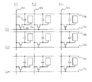
本発明による電気光学装置の一例として液晶装置を用いて説明する。まず、液晶装置の画素について、図1から図4を参照して説明する。図1は、液晶装置の画像表示領域を構成するマトリクス状に形成された複数の画素における各種素子、配線等の等価回路である。図2は、データ線、走査線、画素電極、第1遮光膜等が形成されたTFTアレイ基板の相隣接する複数の画素群並びに対向基板に形成された第1遮光膜及びマイクロレンズの平面図である。図3は、対向基板に形成されたマイクロレンズにより入射光が集光される様子を擬似断面にて示す模式図であり、図4は、図3に示したTFT1個に係るTFTアレイ基板部分を拡大して示す拡大断面図である。尚、図3及び図4においては、各層や各部材を図面上で認識可能な程度の大きさとするため、各層や各部材毎に縮尺を異ならしめてあり、更に、図3では、集光の様子を理解し易く描くために、マイクロレンズ及びTFTの配置関係を、実際の配置関係とは異ならしめてある。即ち、実際には、図2に示すように、マイクロレンズは、そのレンズ中心が各画素中心に一致するように配置されており、TFTは、遮光領域の交点にほぼ対応するように配置されている。
【0043】
図1において、本実施形態による液晶装置の画像表示領域を構成するマトリクス状に形成された複数の画素は、画素電極9aと当該画素電極9aを制御するためのTFT30がマトリクス状に複数形成されており、画像信号が供給されるデータ線6aが当該TFT30のソースに電気的に接続されている。データ線6aに書き込む画像信号S1、S2、…、Snは、この順に線順次に供給しても構わないし、相隣接する複数のデータ線6a同士に対して、グループ毎に供給するようにしても良い。また、TFT30のゲートに走査線3aが電気的に接続されており、所定のタイミングで、走査線3aにパルス的に走査信号G1、G2、…、Gmを、この順に線順次で印加するように構成されている。画素電極9aは、TFT30のドレインに電気的に接続されており、スイッチング素子であるTFT30を一定期間だけそのスイッチを閉じることにより、データ線6aから供給される画像信号S1、S2、…、Snを所定のタイミングで書き込む。画素電極9aを介して電気光学物質としての液晶に書き込まれた所定レベルの画像信号S1、S2、…、Snは、対向基板(後述する)に形成された対向電極(後述する)との間で一定期間保持される。ここで、保持された画像信号がリークするのを防ぐために、画素電極9aと対向電極との間に形成される液晶容量と並列に蓄積容量70を付加する。蓄積容量70を形成するために容量線3bを設けても良いし、前段の走査線3aとの間で蓄積容量70を形成しても良い。例えば、画素電極9aの電圧は、ソース電圧が印加された時間よりも3桁も長い時間だけ蓄積容量70により保持される。これにより、保持特性は更に改善され、コントラスト比の高い液晶装置が実現できる。
【0044】
図2において、液晶装置のTFTアレイ基板上には、マトリクス状に複数の透明な画素電極9a(点線により輪郭が示されている)が設けられており、画素電極9aの縦横の境界に各々沿ってデータ線6a、走査線3a及び容量線3bが設けられている。また、これらの配線の各交点にほぼ対応してTFT30が設けられている。図中、1点鎖線で示されており上下方向に伸びる各データ線6aは、コンタクトホール5を介してポリシリコン膜等からなる半導体層1aのうちTFT30のソース領域に電気接続されている。画素電極9aは、コンタクトホール8を介して半導体層1aのうちTFT30のドレイン領域に電気接続されている。また、図中左右方向に伸びる各走査線3aは、半導体層1aのうちチャネル領域1a’(図中右下りの斜線の領域)に対向するように配置されており、走査線3aはTFT30のゲート電極として機能する。
【0045】
容量線3bは、走査線3aに沿ってほぼ直線状に伸びる本線部と、データ線6aと交差する箇所からデータ線6aに沿って図中上向きに突出した突出部とを有する。そして、半導体層1aは、TFT30から容量線3bに沿って蓄積容量電極1fとして延設されており、この蓄積容量電極1fと容量線3bとが誘電体としての後述の絶縁薄膜を介して対向配置されることにより、蓄積容量が形成されている。
【0046】
図中、1点鎖線で示されており走査線3a及び容量線3bに沿って左右方向に伸びる領域に、複数の縞状部分からなる下地遮光膜11aが設けられていてもよい。より具体的には、下地遮光膜11aは、走査線3a及び容量線3bの本線部に沿って伸びる複数の縞状部分に分断されており、更に各縞状部分は、データ線6aと交差する個所からデータ線6aに沿って図中下方向に夫々突出しており、この突出部により、半導体層1aの少なくともチャネル領域1a’を含む領域を夫々覆うように構成されている。
【0047】
図2には更に、対向基板に、各画素電極11aに夫々対向して形成される複数のマイクロレンズのマイクロレンズ端500aと、対向基板上において複数のマイクロレンズ端500aに夫々対向配置された網目状の第1遮光膜23(図中、右上がりの斜線領域)とが示されている。
【0048】
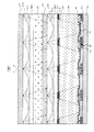
まず、図3の模式図の断面構造の上半分の断面部分について説明する。尚、図3の下半分の断面図部分は図4を用いて詳しく説明する。図3に示されるように、ガラス基板や石英基板からなる対向基板20の外側に設けられた透明基板25には入射光を第1マイクロレンズ500に夫々集光するために各画素に対応してマトリクス状に複数の第2マイクロレンズ503が配置されている。第2マイクロレンズ503の表面全体には第2接着剤504により第2カバーガラス505が貼り付けられている。対向基板20には第2マイクロレンズ503により集光された光を複数の画素電極9aに夫々集光するために各画素に対応して、マトリクス状に複数の第1マイクロレンズ500が配置されている。さらに、複数の第1マイクロレンズ500の相互の境界に夫々対向する位置には第1遮光膜23が形成されている。第1マイクロレンズ500の表面全体には、第1接着剤501により第1カバーガラス502が貼り付けられており、この上に(図中下側に)更に第1遮光膜23及び対向電極21及び配向膜22が順次積層するように形成されている。さらに、第2カバーガラス505はゲル状の接着剤26により対向基板20に接着されている。このように、第2カバーガラス505の面と対向基板20の面とを接着剤26により固着させてもよいし、第2カバーガラス505の周辺と対向基板20の周辺とを接着剤26で固着し、中央部を空気層としてもよい。ゲル状の接着剤26としては、硬化後もゲル状を呈するシリコン系接着剤(弾性を有する接着剤)が用いられ、これにより当該接着剤26を硬化させる際の応力を接着剤26そのものの弾性で吸収させることができる。従って、液晶装置において透明基板25に歪み等が発生することを防止することができる。尚、対向基板20に設けらた第1マイクロレンズ500と透明基板25に設けられた第2マイクロレンズ503とは対応するように、好ましくは互いの光軸が一致し、さらに画素の中央の垂線に一致するように設けると、光の利用効率をさらに向上させることができる。
【0049】
第1マイクロレンズ500は、後述のように、感光性樹脂からなり、第1接着剤501は、空気に近い屈折率を有するアクリル系の接着剤からなり、両者間の屈折率の違いにより、第1マイクロレンズ500は、集光レンズとしての機能を果たす。さらに、第1接着剤501の屈折率と第1マイクロレンズ500の屈折率との関係が
第1接着剤501の屈折率<第1マイクロレンズ500の屈折率
となるように、当該第1接着剤501及び第1マイクロレンズ500の材質が設定されているとよい。
【0050】
尚、第2接着剤504の屈折率と第2マイクロレンズ503の屈折率の関係が、
第2接着剤504の屈折率<第2マイクロレンズ503の屈折率
となるように、当該第2接着剤504及び第2マイクロレンズ503の材質が設定されているとよい。
【0051】
ここで、透明基板25としては例えば石英基板を用いる場合には、その屈折率は1.46なので、対向基板20、第1カバーガラス502、第2カバーガラス505、第1接着剤501、第2接着剤504並びに接着剤26としても当該屈折率に近い屈折率を有する材質を使用することが好ましい。
【0052】
尚、第1接着剤501及び第2接着剤504は、例えばアクリル接着剤を用いる。
【0053】
上述の構成によれば、対向基板20上に備えられた第1マイクロレンズ500及び第2マイクロレンズ503により、対向基板20側からの入射光は、複数の画素電極9a上に夫々集光される。従って、第1マイクロレンズ500及び第2マイクロレンズ503が無い場合と比較して、各画素における実効開口率が高められている。また、上述のように透明基板25に入射された光は第2マイクロレンズ503により集光されて対向基板20に入射し、さらに対向基板20に入射される光は第1マイクロレンズ500により集光されて画素電極9aに集光される。即ち、対向基板20には透明基板25に配置された第2マイクロレンズ503により集光された光が入射されるため、対向基板20の集光領域から第1遮光膜23を外して配置でき、入射光が第1遮光膜23によりさまたげられるのを防ぎ、光損失を防ぐことができる。しかも入射光が第1マイクロレンズ500の境界を通過して、TFT30のチャネル領域に直接入射したり、多重反射等により迷光となった後に入射する事態を未然に防げる。さらにまた、第1遮光膜23の存在により、対向基板20における機械的強度及び熱遮断性能は各々、当該第1遮光膜23がなかった場合と比較して顕著に高められる。さらに、本実施形態は、基板外面に付着する塵埃、傷等をデフォーカスさせる効果がある。即ち、透明基板25を有さない構成を例えば投射型表示装置に用いた場合、対向基板20の外面は、集光光学系によりフォーカスされている液晶装置の液晶層に対して1mm程度しか離れていないため対向基板20の外面もフォーカス状態にあり、このため、10〜20μm程度の塵埃や傷が存在しても拡大投射されて投射画像の画質を著しく低下させるという問題点がある。しかし、本実施形態の如く対向基板20の外側に透明基板25を有する場合、塵埃や傷は対向基板20ではなく透明基板25のほうに付着されやすくなる。そのため、透明基板25を対向基板20に面接着すれば、たとえ透明基板25の外面に塵埃や傷ががついても、これらの塵埃や傷は液晶層50から離れデフォーカスされるので表示品位の低下を防止することができる。この場合、透明基板25は対向基板20と同等の厚さもしくはそれ以上の厚さを有すれば、塵埃等をデフォーカスするために効果的である。
【0054】
上記の構成に加えて、本実施形態の特徴となる構成について図2及び図4を用いて説明する。
【0055】
図4は、図3の下半分の断面構造に関し、特に図3に示したTFT30の1個に係わるTFTアレイ基板10部分を拡大して示す拡大断面図である。図4に示されるように、TFTアレイ基板10には、画素電極9aが設けられており、その上側には、ラビング処理等の所定の配向処理が施された配向膜16が設けられている。画素電極9aは例えば、ITO(Indium Tin Oxide)膜などの透明導電性薄膜からなる。また配向膜16は例えば、ポリイミド薄膜などの有機薄膜からなる。
【0056】
図4に示すように、TFTアレイ基板10には、各画素電極9aに隣接する位置に、各画素電極9aをスイッチング制御する画素スイッチング用TFT30が設けられている。
【0057】
このように構成され、画素電極9aと対向電極21とが対面するように配置されたTFTアレイ基板10と対向基板20との間には、後述のシール材(図13及び図14参照)により囲まれた空間に電気光学物質である液晶が封入され、液晶層50が形成される。液晶層50は、画素電極9aからの電界が印加されていない状態で配向膜16及び図3に示した配向膜22により所定の配向状態を採る。液晶層50は、例えば一種又は数種類のネマティック液晶を混合した液晶からなる。シール材は、TFTアレイ基板10及び対向基板20をそれらの周辺で貼り合わせるための、例えば光硬化性樹脂や熱硬化性樹脂からなる接着剤であり、両基板間の距離を所定値とするためのグラスファイバー或いはガラスビーズ等のスペーサが混入されている。
【0058】
図4に示すように、画素スイッチング用TFT30に各々対向する位置においてTFTアレイ基板10と各画素スイッチング用TFT30との間には、下地遮光膜11aが設けられている。下地遮光膜11aは、好ましくは不透明な高融点金属であるTi(チタン)、Cr、W(タングステン)、Ta(タンタル)、Mo(モリブデン)及びPb(鉛)のうちの少なくとも一つを含む、金属単体、合金、金属シリサイド等から構成される場合がある。このような材料から構成すれば、TFTアレイ基板10上の下地遮光膜11aの形成工程の後に行われる画素スイッチング用TFT30の形成工程における高温処理により、下地遮光膜11aが破壊されたり溶融しないようにできる。
【0059】
また、下地遮光膜11aと複数の画素スイッチング用TFT30との間には、第1層間絶縁膜12が設けられている。第1層間絶縁膜12は、画素スイッチング用TFT30を構成する半導体層1aを下地遮光膜11aから電気的絶縁するために設けられるものである。更に、第1層間絶縁膜12は、TFTアレイ基板10の全面に形成されることにより、画素スイッチング用TFT30のための下地膜としての機能をも有する。即ち、TFTアレイ基板10の表面の研磨時における荒れや、洗浄後に残る汚れ等で画素スイッチング用TFT30の特性の劣化を防止する機能を有する。第1層間絶縁膜12は、例えば、NSG(ノンドープトシリケートガラス)、PSG(リンシリケートガラス)、BSG(ボロンシリケートガラス)、BPSG(ボロンリンシリケートガラス)などの高絶縁性ガラス又は、酸化シリコン膜、窒化シリコン膜等からなる。第1層間絶縁膜12により、下地遮光膜11aが画素スイッチング用TFT30等を汚染する事態を未然に防ぐこともできる。
【0060】
図4において、画素スイッチング用TFT30は、LDD(Lightly Doped Drain)構造を有しており、走査線3a、当該走査線3aからの電界によりチャネルが形成される半導体層1aのチャネル領域1a’、走査線3aと半導体層1aとを絶縁する絶縁薄膜2、データ線6a、半導体層1aの低濃度ソース領域1b及び低濃度ドレイン領域1c、半導体層1aの高濃度ソース領域1d並びに高濃度ドレイン領域1eを備えている。高濃度ドレイン領域1eには、複数の画素電極9aのうちの対応する一つが接続されている。本実施形態では特にデータ線6aは、Al等の低抵抗な金属膜や金属シリサイド等の合金膜などの遮光性の薄膜から構成されている。また、走査線3a、絶縁薄膜2及び第1層間絶縁膜12の上には、第2層間絶縁膜4が形成されている。第2層間絶縁膜4に形成されたコンタクトホール5を介して、データ線6aは高濃度ソース領域1dに電気接続されている。更に、データ線6a及び第2層間絶縁膜4の上には、第3層間絶縁膜7が形成されている。第3層間絶縁膜7に形成されたコンタクトホール8を介して、画素電極9aは高濃度ドレイン領域1eに電気接続されている。画素電極9aは、このように構成された第3層間絶縁膜7の上面に設けられている。尚、画素電極9aと高濃度ドレイン領域1eとは、データ線6aと同一のAl膜や走査線3bと同一のポリシリコン膜を中継しての電気接続するようにしてもよい。
【0061】
本実施形態では、絶縁薄膜2を走査線3aに対向する位置から延設して誘電体膜として用い、半導体層1aを延設して第1蓄積容量電極1fとし、更にこれらに対向する容量線3bの一部を第2蓄積容量電極とすることにより、蓄積容量70が構成されている。より詳細には、半導体層1aの高濃度ドレイン領域1eが、データ線6a及び走査線3aの下に延設されて、同じくデータ線6a及び走査線3aに沿って伸びる容量線3b部分に絶縁薄膜2を介して対向配置されて、第1蓄積容量電極1fとされている。特に蓄積容量70の誘電体としての絶縁薄膜2は、高温酸化によりポリシリコン膜上に形成されるTFT30のゲート絶縁膜としても機能するので、薄く且つ高耐圧の絶縁膜とすることができ、蓄積容量70は比較的小面積で大容量の蓄積容量として構成できる。
【0062】
この結果、データ線6a下の領域及び走査線3aに沿って液晶のディスクリネーションが発生する領域(即ち、容量線3bが形成された領域)という開口領域を外れたスペースを有効に利用して、画素電極9aの蓄積容量を増やすことが出来る。
【0063】
このような構成において、本実施形態では特に、図2に示されるように、TFTアレイ基板の網目状の遮光領域は、下地遮光膜11aと遮光性の金属膜の一例としてのAl(アルミニウム)膜からなるデータ線6aとから、網目状の第1遮光膜23は平面的に、この遮光領域により覆われている。即ち、平面的に見て第1遮光膜23の輪郭は、遮光領域の輪郭内に含まれている。そして、遮光領域に囲まれた各画素電極9aにより、入射光が透過する領域である画素開口領域が規定されている。第1マイクロレンズ500により集光された入射光は、図中、破線で示される円形の集光領域500bに集光される。即ち、入射光は下地遮光膜11a及びデータ線6aにより規定される遮光領域(図2参照)内に、即ち第1マイクロレンズ500による画素電極9a上の集光領域500bから外れて位置する。このため、対向基板20側からの入射光が第1マイクロレンズ500を介してTFT30のチャネル領域1a'に入射することは実用上殆ど又は全くない。さらに、TFTアレイ基板10と対向基板20を機械的に貼り合わせる際の組みずれにより、遮光領域(或いは、下地遮光膜11a)に対して第1遮光膜23が平面的にずれてたとしても、両輪郭間の距離に応じて、第1遮光膜23の下地遮光膜11a或いはデータ線6aからの平面的なはみ出しは、全部或いは部分的に吸収される。言い換えれば、第1遮光膜23は、遮光領域或いは画素開口領域を規定する機能を持たず、上述のように第1マイクロレンズ500の境界にだけ最低限設けておけば足りるので、TFTアレイ基板10と対向基板20とを接着する際の組みずれを見込んで、第1遮光膜23の形成領域を小さめに設定しておくことにより、この組みずれが画素開口率には何等影響しないようにできる。このため、所定許容範囲内にある多少の組みずれによっては、画素開口領域は全く狭くならないか或いは少ししか狭くならないで済む。
【0064】
以上のように、仮にTFT30のチャネル領域1a’における対向基板20側の遮光を金属薄膜からなるデータ線6aにより施さなくても、対向基板20側からの入射光に対するTFT30のチャネル領域1a’における遮光は、マイクロレンズ500及び第1遮光膜23により十分に施される。他方、前述のように下地遮光膜11aにより、各TFT30のチャネル領域1a’は、TFTアレイ基板10側から見て夫々覆われる。従って、TFTアレイ基板10側からの戻り光等がTFT30のチャネル領域1a’に入射してTFT30のトランジスタ特性が劣化する事態を未然に防ぐことが出来る。以上の結果、入射光や戻り光等のTFT30のチャネル領域1a’への入射により、TFT30の特性が劣化することは実践上殆ど又は全く無く、本実施形態の液晶装置では、TFT30による精度の高い液晶駆動が可能とされる。
【0065】
これらに加えて、下地遮光膜11aとデータ線6aとにより規定される遮光領域は、コントラストの向上、色材の混色防止などの機能をも有する。
【0066】
更にまた、第1遮光膜23は、上述のように画素開口率にほぼ又は全く影響しないので、従来のCr等と比べて寸法精度が出ない材料を第1遮光膜23の材料として使用することも可能となる。従って、従来のCr等と比べて反射率が高いが精度を出し難い、例えばAl等の材料を第1遮光膜23として使用することも可能となる。Al膜は反射率が例えば90数パーセントといったように従来のCrに比べて非常に高くできる。これにより仮に対向基板20側から入射する入射光が第1遮光膜23にあたったとしても、高反射率で反射することが出来るので、第1遮光膜23の形成面積に応じて当該液晶装置の温度上昇をより効率的に抑えることも可能となる。
【0067】
本実施形態では特に、図2乃至図4に示したように、画素電極9a上において第1マイクロレンズ500の集光領域500bにはみ出さないように第1マイクロレンズ500の集光角度に応じて、下地遮光膜11a及びデータ線6aからなる遮光領域が規定されている。ここで、第1マイクロレンズ500の集光角度或いは集光能力が大きい程、画素電極9a上における集光領域500bの面積は小さくなるので、このように集光領域500bにはみ出さない範囲で、遮光領域を大きく設定すれば、第1マイクロレンズ500の集光角度によらず、下地遮光膜11a及び第1遮光膜23における遮光による光損失を低く抑えられる。従って、各種の曲率や形状を持つ第1マイクロレンズ500を用いて本実施形態の液晶装置を構成することが可能となる。
【0068】
更にまた、コンタクトホール5は、対向基板20の側から見てデータ線6aの下に開孔されている。このため、コンタクトホール5は、画素の開口領域から外れており、しかも画素スイッチング用TFT30や第1蓄積容量電極1fが形成されていない第1層間絶縁膜12の部分に設けられているので、画素領域の有効利用を図りつつ、コンタクトホール5の形成によるTFT30や他の配線等の不良化を防ぐことができる。
【0069】
以上説明したように、本実施形態の液晶装置により、比較的簡単な構成を用いて、各画素における実効開口率を高めつつ、高精細な画像を表示できる。
【0070】
(マイクロレンズの製造方法)
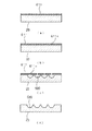
次に、本実施形態に用いられる第1マイクロレンズ500及び第2マイクロレンズ503の製造方法について、第1マイクロレンズ500を例として図5を参照して説明する。
【0071】
先ず図5(a)に示すように、ネオセラム等のガラス基板や石英基板からなる対向基板20上に、感光性樹脂510を塗布する。
【0072】
次に図5(b)に示すように、各第1マイクロレンズ500となる部分に対応する凸部が残るように所定パターンを有するマスク520を介して、感光性樹脂510をマスク露光し、その後、図5(c)に示すように、ウェット又はドライエッチングにより現像する。
【0073】
次に図5(d)に示すように、熱フローを印加し、感光性樹脂510の熱変形及び表面張力により、滑らかな各マイクロレンズの凸面を持つ感光性樹脂510からなる、図2及び図3に示したような複数のマイクロレンズ500を形成する。この際特に、熱フローを基板面上で制御することにより、所定の集光能力を有し且つ隙間が殆ど空かないように複数の第1マイクロレンズ500を形成する。
【0074】
次に図5(e)に示すように、第1マイクロレンズ500の表面にアクリル系接着剤501を塗布してネオセラム等からなるカバーガラス502gを接着する。
【0075】
次に図5(f)に示すように、カバーガラス502gを研磨して、図3に示した如き、所定の厚みを有するカバーガラス502とする。
【0076】
最後に図5(g)に示すように、第1遮光膜23及び対向電極21をスパッタリング、コーティング等によりこの順に成膜して、図3に示した如き第1マイクロレンズ500及び第1遮光膜23を備えた対向基板20を完成させる。上記の製造方法によれば、凸型のマイクロレンズが形成されるが、凹型のマイクロレンズとしては次の製造方法について図6を用いて説明する。
【0077】
先ず図6(a)に示すように、ネオセラム等のガラス基板や石英基板からなる対向基板20上に、マスク層611を形成する。
【0078】
次に図6(b)に示すように、マスク層611に所定の平面配列で開口部611aをフォトリソグラフィ法のパターニング処理により形成する。この時、開口部611aの開口径は実際に形成しようとする凹曲面部の径よりも小さいことが望ましい。
【0079】
次に、図6(c)に示すように、マスク層611の開口部611aから対向基板20の表面を等方的にエッチング処理し、凹曲面部600を形成する。このエッチング処理は、フッ酸を主体とするエッチング液を用いた湿式エッチングで行う。
【0080】
次に、図6(d)に示すようにマスク層611をエッチング処理によって除去する。図6(d)以降の工程は、上述の凹型マイクロレンズの製造方法の図5(e)以降と同様な工程を有するため、その説明及び図示を省略する。
【0081】
尚、第1マイクロレンズ500は、例えば、特開平6−194502号公報に開示されている公知の製造方法や伝統的な所謂「熱変形法」により形成してもよい。このように形成された第1マイクロレンズ500を有する対向基板20をシール材を介してTFTアレイ基板10と貼りあわせる。第2マイクロレンズ503を有する透明基板25は、第1マイクロレンズ500と図5(g)までは同様の工程で形成し、第1遮光膜23及び対向電極21は形成しないようにする。その後、第1マイクロレンズを有する対向基板20と第2マイクロレンズ503を有する透明基板25とをゲル状の接着剤26により貼りあわせる。この接着剤26を対向基板20と透明基板25の面接着させてもよいが、対向基板20と透明基板25のそれぞれの対向する面の周辺で接着剤により固着させて、中央部を空気層としても良い。また、第1マイクロレンズと第2マイクロレンズとを同一平面構造を有するようにすれば、同一工程で夫々のマイクロレンズを作成することができ、歩留まりを向上させることができる。また、同一平面構造を有すれば第2マイクロレンズ503で集光されなかった投射光を第1マイクロレンズ500で集光することができ、投射光の利用効率を高めることができる。
【0082】
〔第2実施形態〕
次に、本発明に係る液晶装置の第2実施形態について、図7を用いて説明する。
【0083】
なお、図7は第2実施形態に係る液晶装置の構造を示す断面模式図である。
【0084】
また、第2実施形態の液晶装置の全体構成及び平面形状は第1実施形態の液晶装置と同一であるので、細部の説明は省略する。
【0085】
上述の第1実施形態においては、対向基板20上に第1マイクロレンズ500を形成すると共に、透明基板25上に第2マイクロレンズ503を形成する構成としたが、第2実施形態では、対向基板20の両面に第1マイクロレンズ500と第2マイクロレンズ503を形成している。
【0086】
その他のTFTアレイ基板10の構成等は第1実施形態の液晶装置と同一であるので、細部の説明は省略する。
【0087】
このとき、投射光を画素電極9aへ集光させるためには、第2マイクロレンズ503の屈折率と第2接着剤504の屈折率との関係について、
第2マイクロレンズ503の屈折率<第2接着剤504の屈折率
となる関係にあり、一方、第1マイクロレンズ500の屈折率と第1接着剤501の屈折率との関係については、
第1マイクロレンズ500の屈折率>第1接着剤501の屈折率
となる関係になる。
【0088】
なお、対向基板20の両面に第1マイクロレンズ500及び第2マイクロレンズ503を形成するための製造方法としては、上述した図5における第1工程乃至第4工程(図5(a)乃至図5(d)に示す。)を対向基板20の両面について同様に形成し、第1マイクロレンズ500側に第1遮光膜23、対向電極21、配向膜22を形成すればよい。
【0089】
以上説明したように、第2実施形態の液晶装置の構成によっても、第1マイクロレンズに第1遮光膜23を形成した場合でも投射光の利用効率を向上させることができる。
【0090】
更に、この効果に加えて、第2マイクロレンズ503を画素電極9aに対してより近い位置に配置することができるので、必要な投射光の集光を得るために必要な第2マイクロレンズ503の平面形状をより小さくできる。
【0091】
更に、第2マイクロレンズ503自体を薄くして液晶装置全体を薄くできるので、第2実施形態の構成は液晶装置の小型化に好適である。
【0092】
〔第3実施形態〕
次に、本発明に係る液晶装置の第3実施形態について、図8を用いて説明する。
【0093】
なお、図8は第3実施形態に係る液晶装置の構造を示す断面模式図である。
【0094】
また、第3実施形態の液晶装置の全体構成及び平面形状は第1実施形態の液晶装置と同一であるので、細部の説明は省略する。
【0095】
上述の第1実施形態においては、対向基板20上に第1マイクロレンズ500を形成すると共に、透明基板25上に第2マイクロレンズ503を形成し、当該第2マイクロレンズ503を接着剤26及び第2カバーガラス504を介して対向基板20に接着する構成としたが、第3実施形態では、当該第2マイクロレンズ503が形成された透明基板25を第2接着剤504により直接対向基板20に接着する構成としている。
【0096】
その他のTFTアレイ基板10の構成等は第1実施形態の液晶装置と同一であるので、細部の説明は省略する。
【0097】
このとき、投射光を画素電極9aへ集光させるためには、第2マイクロレンズ503の屈折率と第2接着剤504の屈折率との関係について、
第2マイクロレンズ503の屈折率>第2接着剤504の屈折率
なる関係があり、一方、第1マイクロレンズ500の屈折率と第1接着剤501の屈折率との関係については、
第1マイクロレンズ500の屈折率>第1接着剤501の屈折率
なる関係が必要となる。
【0098】
また、対向基板20に第1マイクロレンズ500を形成する製造方法及び透明基板25に第2マイクロレンズ503を形成する製造方法は、それぞれ図5における製造方法を用いて形成することができる。
【0099】
以上説明したように、第3実施形態の液晶装置の構成によれば、第2実施形態の液晶装置の構成の効果と同様の効果を奏することができる。
【0100】
〔第4実施形態〕
次に、本発明に係る液晶装置の第4実施形態について、図9を用いて説明する。
【0101】
なお、図9は第4実施形態に係る液晶装置の構造を示す断面模式図である。
【0102】
また、第4実施形態の液晶装置の全体構成及び平面形状は第1実施形態の液晶装置と同一であるので、細部の説明は省略する。
【0103】
上述の第1乃至第3実施形態においては、第1マイクロレンズ500又は第2マイクロレンズ503を凸レンズとして形成したが、第4実施形態では、対向基板20に形成される第1マイクロレンズ500及び透明基板25に形成される第2マイクロレンズ503を夫々凹レンズとして形成している。
【0104】
その他のTFTアレイ基板10の構成等は第1実施形態の液晶装置と同一であるので、細部の説明は省略する。
【0105】
このとき、投射光を画素電極9aへ集光させるためには、第2マイクロレンズ503の屈折率と第2接着剤504の屈折率との関係について、
第2マイクロレンズ503の屈折率<第2接着剤504の屈折率
なる関係があり、一方、第1マイクロレンズ500の屈折率と第1接着剤501の屈折率との関係については、
第1マイクロレンズ500の屈折率<第1接着剤501の屈折率
なる関係がある。
【0106】
以上説明したように、第4実施形態の液晶装置の構成によれば、第2実施形態の液晶装置又は第3実施形態の液晶装置と同様の効果を奏することができる。
【0107】
また、対向基板20に第1マイクロレンズ500を形成する製造方法及び透明基板25に第2マイクロレンズ503を形成する製造方法は、それぞれ図6における製造方法を用いて形成することができる。
【0108】
〔第5実施形態〕
次に、本発明に係る液晶装置の第5実施形態について、図10を用いて説明する。
【0109】
なお、図10は第5実施形態に係る液晶装置の構造を示す断面模式図である。
【0110】
また、第5実施形態の液晶装置の全体構成及び平面形状は第1実施形態の液晶装置と同一であるので、細部の説明は省略する。
【0111】
上述の第4実施形態においては、凹レンズ型の第1マイクロレンズ500を対向基板20上に形成し、他方凹レンズ型の第2マイクロレンズ503を透明基板25上に形成したが、第5実施形態では、対向基板20の両面に夫々凹レンズ型の第1マイクロレンズ500及び第2マイクロレンズ503を形成している。
【0112】
その他のTFTアレイ基板10の構成等は第1実施形態の液晶装置と同一であるので、細部の説明は省略する。
【0113】
このとき、投射光を画素電極9aへ集光させるためには、第2マイクロレンズ503の屈折率と第2接着剤504の屈折率との関係について、
第2マイクロレンズ503の屈折率>第2接着剤504の屈折率
なる関係があり、一方、第1マイクロレンズ500の屈折率と第1接着剤501の屈折率との関係については、
第1マイクロレンズ500の屈折率<第1接着剤501の屈折率
なる関係が必要となる。
【0114】
以上説明したように、第5実施形態の液晶装置の構成によれば、第2実施形態の液晶装置から第4実施形態の液晶装置うちのいずれか一の液晶装置と同様の効果を奏することができる。
【0115】
また、対向基板20に第1マイクロレンズ500及びマイクロレンズ503を形成する製造方法は、それぞれ図6における製造方法を用いて形成することができる。
【0116】
〔第6実施形態〕
次に、本発明に係る液晶装置の第6実施形態について、図11を用いて説明する。
【0117】
なお、図11は第6実施形態に係る液晶装置の構造を示す断面模式図である。
【0118】
また、第6実施形態の液晶装置の全体構成及び平面形状は第1実施形態の液晶装置と同一であるので、細部の説明は省略する。
【0119】
上述の第4実施形態又は第5実施形態においては、第1マイクロレンズ500及び第2マイクロレンズ503を双方とも凹レンズ形状としたが、第6実施形態では、第1マイクロレンズ500を凹レンズ型とし、一方で第2マイクロレンズ503を凸レンズ型とし、更に、第1マイクロレンズ500及び第2マイクロレンズ503の双方を対向基板20の両面に形成している。
【0120】
その他のTFTアレイ基板10の構成等は第1実施形態の液晶装置と同一であるので、細部の説明は省略する。
【0121】
このとき、投射光を画素電極9aへ集光させるためには、第2マイクロレンズ503の屈折率と第2接着剤504の屈折率との関係について、
第2マイクロレンズ503の屈折率>第2接着剤504の屈折率
なる関係があり、一方、第1マイクロレンズ500の屈折率と第1接着剤501の屈折率との関係については、
第1マイクロレンズ500の屈折率<第1接着剤501の屈折率
なる関係が必要となる。
【0122】
なお、対向基板20の片面に凸レンズ型の第2マイクロレンズ503を形成するためには、上述した図5における第1工程乃至第4工程(図5(a)乃至図5(d)に示す。)を対向基板20の当該片面について行えばよい。
【0123】
以上説明したように、第6実施形態の液晶装置の構成によれば、第2実施形態の液晶装置から第5実施形態の液晶装置うちのいずれか一の液晶装置と同様の効果を奏することができる。
【0124】
また、対向基板20に第1マイクロレンズ500を形成する製造方法は図6のおける製造方法を用いて、第2マイクロレンズ503を形成する製造方法は、図5における製造方法を用いて形成することができる。
【0125】
〔第7実施形態〕
次に、本発明に係る液晶装置の第7実施形態について、図12を用いて説明する。
【0126】
なお、図12は第7実施形態に係る液晶装置の構造を示す断面模式図である。
【0127】
また、第7実施形態の液晶装置の全体構成及び平面形状は第1実施形態の液晶装置と同一であるので、細部の説明は省略する。
【0128】
上述の第6実施形態においては、第1マイクロレンズ500を凹レンズ型とし、第2マイクロレンズ503を凸レンズ型としたが、第7実施形態では、第1マイクロレンズ500を凸レンズ型とし、一方で第2マイクロレンズ503を凹レンズ型とし、更に、第1マイクロレンズ500及び第2マイクロレンズ503の双方を対向基板20の両面に形成している。
【0129】
その他のTFTアレイ基板10の構成等は第1実施形態の液晶装置と同一であるので、細部の説明は省略する。
【0130】
このとき、投射光を画素電極9aへ集光させるためには、第2マイクロレンズ503の屈折率と第2接着剤504の屈折率との関係について、
第2マイクロレンズ503の屈折率<第2接着剤504の屈折率
なる関係があり、一方、第1マイクロレンズ500の屈折率と第1接着剤501の屈折率との関係については、
第1マイクロレンズ500の屈折率>第1接着剤501の屈折率
なる関係が必要となる。
【0131】
なお、対向基板20の片面に凸レンズ型の第1マイクロレンズ500を形成するためには、上述した図5における第1工程乃至第4工程(図5(a)乃至図5(d)に示す。)を対向基板20の当該片面について行えばよい。
【0132】
以上説明したように、第7実施形態の液晶装置の構成によれば、第2実施形態の液晶装置から第6実施形態の液晶装置うちのいずれか一の液晶装置と同様の効果を奏することができる。
【0133】
また、対向基板20に第1マイクロレンズ500を形成する製造方法は図5における製造方法を用いることができ、また対向基板20に第2マイクロレンズ503を形成する製造方法は、それぞれ図6における製造方法を用いて形成することができる。
【0134】
なお、上述の各実施形態においては、各画素電極9aに設けられているTFT30としては、正スタガ型又はコプラナー型等のポリシリコン薄膜TFTであるとして説明したが、これ以外に、逆スタガ型のTFTやアモルファスシリコンTFT等の他形式のトランジスタに対しても、各実施形態は有効である。
【0135】
また、各実施形態では、TFTを用いて画素電極9aに駆動電圧を印加するように構成したが、TFT以外の、例えぱ、TFD(Thin Film Diode:薄膜ダイオード)等のアクティブマトリクス素子を用いることも可能であり、更に、液晶装置をパッシブマトリクス型の液晶装置として構成することも可能である。
【0136】
このような場合であっても、マイクロレンズで画素電極上に投射光を集光する構成を採る限り、投射光の利用効率を向上させる上で本実施形態の場合と同様に有効である。
【0137】
更に、第2マイクロレンズ503の配置については、これを透明基板25の更に外側に設けてもよい。
【0138】
更にまた、透明基板250の液晶層50に対向している面と反対の面(投射光の出射面)に、第1マイクロレンズ500及び第2マイクロレンズ503で集光した投射光を平行光に戻すためのマイクロレンズを更に設ける構成としてもよい。
【0139】
次に、対向基板20上における第1遮光膜23の形状については、図13(A)から図13(C)に示すように各種の形状とすることが可能である。
【0140】
先ず、図2に示したと同様に、図13(A)に示すように、右下がりの斜線はTFTアレイ基板10上の走査線3a、データ線6a、TFT30等により規定される遮光領域を示し、この遮光領域は右上がりの斜線で示される前記第1遮光膜23により平面的に覆われるように、第1遮光膜23を網目状に形成してもよい。このように遮光領域に覆われる範囲で第1遮光膜23の形成領域を大きくすれば、電気光学装置内部へ入射しようとする入射光に対する第1遮光膜23の遮光や反射の機能を向上でき、これに応じて電気光学装置における温度上昇を抑制できる。さらに、遮光領域の機能を第1遮光膜に冗長的に持たせることができる。
【0141】
或いは、図13(B)に示すように、右下がりの斜線で示す遮光領域により平面的に覆われる右上がりの斜線で示した領域に、走査線3aに沿って(図中、左右方向に)伸びる縞状の第1遮光膜23’を形成してもよい。形成が比較的容易な縞状の輪郭を持つ第1遮光膜23’により、電気光学装置内部へ入射しようとする入射光を遮光や反射できるので、電気光学装置における温度上昇を抑制することができる。
【0142】
或いは、図13(C)に示すように、右下がりの斜線で示す遮光領域により平面的に覆われる右上がりの斜線で示した領域に、走査線に沿って画素毎に分断された島状の第1遮光膜23”を形成してもよい。
【0143】
この態様によれば、形成が比較的容易な島状の輪郭を持つ第1遮光膜23”により、電気光学装置内部へ入射しようとする投射光を遮光や反射できるので、電気光学装置における温度上昇を抑制できる。特に第1遮光膜23”は遮光領域を規定する機能をもたなくても、対向基板における強度を出すために必要最低限の領域にのみ、島状に第1遮光膜23”を形成することにより、TFTアレイ基板と対向基板20の貼り合わせ精度にマージンを持たせることができる。
【0144】
これら図13(A)から図13(C)に示したいずれの形態によっても、対向基板20の強度を高めることが出来ると共に、液晶層への熱入射を低減することが出来る。上記3つの形状は、第1実施形態1乃至第7実施形態のいずれにも適用可能である。
【0145】
また、上述の実施形態では、第1マイクロレンズ500で集光された光をさらに第2マイクロレンズ503により集光するようにしたが、入射光を第2マイクロレンズ503により平行光にすることも可能である。このように第1マイクロレンズで集光された光をさらに第2マイクロレンズにより平行光になるように集光すれば、入射光が画素領域に局部的に集光するのを緩和し、入射光による液晶あるいは配向膜等の劣化を防ぐことができる。
【0146】
(液晶装置の全体構成)
以上のように構成された液晶装置の各実施形態の全体構成を図14から図15を参照して説明する。図14は、TFTアレイ基板10をその上に形成された各構成要素と共に対向基板20の側から見た平面図であり、図15は、対向基板20を含めて示す図14のH−H’断面図である。
【0147】
図14において、TFTアレイ基板10の上には、シール材52がその縁に沿って設けられており、その内側に並行して、例えば第1遮光膜23と同じ或いは異なる材料から成る額縁としての第2遮光膜53が設けられている。シール材52の外側の領域には、データ線駆動回路101及び外部回路接続端子102がTFTアレイ基板10の一辺に沿って設けられており、走査線駆動回路104が、この一辺に隣接する2辺に沿って設けられている。走査線3aに供給される走査信号遅延が問題にならないのならば、走査線駆動回路104は片側だけでも良いことは言うまでもない。また、データ線駆動回路101を画像表示領域の辺に沿って両側に配列してもよい。例えば奇数列のデータ線6aは画像表示領域の一方の辺に沿って配設されたデータ線駆動回路101から画像信号を供給し、偶数列のデータ線6aは前記画像表示領域の反対側の辺に沿って配設されたデータ線駆動回路101から画像信号を供給するようにしてもよい。この様にデータ線6aを櫛歯状に駆動するようにすれば、データ線駆動回路101の占有面積を拡張することができるため、複雑な回路を構成することが可能となる。更にTFTアレイ基板10の残る一辺には、画像表示領域の両側に設けられた走査線駆動回路104間をつなぐための複数の配線105が設けられている。また、対向基板20のコーナー部の少なくとも1箇所においては、TFTアレイ基板10と対向基板20との間で電気的導通をとるための導通材106が設けられている。そして、図15に示すように、図14に示したシール材52とほぼ同じ輪郭を持つ対向基板20が当該シール材52によりTFTアレイ基板10に固着されている。
【0148】
以上説明した各実施形態における液晶装置は、カラー液晶プロジェクタに適用されるため、3枚の液晶装置がRGB用のライトバルブとして各々用いられ、各液晶装置には各々RGB色分解用のダイクロイックミラーを介して分解された各色の光が投射光として各々入射されることになる。従って、各実施形態では、対向基板20に、カラーフィルタは設けられていない。しかしながら、第1遮光膜23の形成されていない画素電極9aに対向する所定領域にRGBのカラーフィルタをその保護膜と共に、対向基板20上に形成してもよい。このようにすれば、液晶プロジェクタ以外の直視型や反射型のカラー液晶テレビなどのカラー液晶装置に各実施形態における液晶装置を適用できる。更にまた、対向基板20上に、何層もの屈折率の相違する干渉層を堆積することで、光の干渉を利用して、RGB色を作り出すダイクロイックフィルタを形成してもよい。このダイクロイックフィルタ付き対向基板によれば、より明るいカラー液晶装置が実現できる。
【0149】
また従来は、TFTアレイ基板10の裏面側での反射を防止するために、反射防止用のAR(Anti Reflection)被膜された偏光板を別途配置したり、ARフィルムを貼り付ける必要があった。しかし、各実施形態では、TFTアレイ基板10の表面と半導体層1aの少なくともチャネル領域1a’に下地遮光膜11aが形成されているため、このようなAR被膜された偏光板やARフィルムを用いたり、TFTアレイ基板10そのものをAR処理した基板を使用する必要が無くなる。従って、各実施形態によれば、材料コストを削減でき、また偏光板貼り付け時に、ごみ、傷等により、歩留まりを落とすことがなく大変有利である。また、耐光性が優れているため、明るい光源を使用したり、偏光ビームスプリッタにより偏光変換して、光利用効率を向上させても、光によるクロストーク等の画質劣化を生じない。
【0150】
更にまた、第1マイクロレンズ500及び第2マイクロレンズ503の集光能力としては、集光領域500b(図2参照)が開口領域に丁度収まる程度に集光できれば十分であり、必要以上に集光領域500bを小さくする必要はない。更に、第1マイクロレンズ500及び第2マイクロレンズ503により、各画素における実効開口率が高められているので、画素開口領域を広げるために、走査線3a、容量線3b及びデータ線6aの線幅やTFT30の平面的なサイズを必要以上に小さくする必要はない。従って、本実施形態は、画素ピッチを小さくして、各画素の微細化を行う場合に非常に適している。
【0151】
また、液晶装置に限らず、各種の電気光学装置、例えばエレクトロルミネッセンス、プラズマディスレプレイ等の電気光学装置に本実施形態は有効である。
【0152】
図16に本実施形態を用いた応用例として液晶プロジェクタの構成について説明する。液晶プロジェクタ1100は、上述の電気光学装置としての液晶装置を含む液晶モジュールを3個用意し、各々RGB用のライトバルブ100R、100G及び100Bとして用いたプロジェクタとして構成されている。液晶プロジェクタ1100では、メタルハライドランプ等の白色光源のランプユニット1102から投射光が発せられると、3枚のミラー1106及び2枚のダイクロイックミラー1108によって、RGBの3原色に対応する光成分R、G、Bに分けられ、各色に対応するライトバルブ100R、100G及び100Bに各々導かれる。この際特にB光は、長い光路による光損失を防ぐために、入射レンズ1122、リレーレンズ1123及び出射レンズ1124からなるリレーレンズ系1121を介して導かれる。そして、ライトバルブ100R、100G及び100Bにより各々変調された3原色に対応する光成分は、ダイクロイックプリズム1112により再度合成された後、投射レンズ1114を介してスクリーン1120にカラー画像として投射される。
【0153】
本実施形態では特に、下地遮光膜11aがTFT30の下側にも設けられているため、当該液晶装置からの投射光に基づく液晶プロジェクタ内の投射光学系による反射光、投射光が通過する際の液晶装置用基板の表面からの反射光、他の液晶装置から出射した後にダイクロイックプリズム1112を突き抜けてくる投射光の一部等が、戻り光として液晶装置用基板の側から入射しても、画素電極9aのスイッチング用のTFT等30のチャネル領域1aに対する遮光を十分に行うことができる。このため、小型化に適したプリズムを投射光学系に用いても、各液晶装置の液晶装置用基板とプリズムとの間において、戻り光防止用のARフィルムを貼り付けたり、偏光板にAR被膜処理を施したりすることが不要となるので、構成を小型且つ簡易化する上で大変有利である。
【0154】
さらに、本実施形態は、下地遮光膜によりチャネル領域への戻り光を防ぐことができるため、液晶装置に戻り光防止処理を施した偏光板を直接貼りつけず、偏光板を液晶装置から離して形成するようにしてもよい。より具体的には、一方の偏光板(図示せず)をダイクロイックプリズム1112に貼り付けることが可能である。このように、偏光板をプリズムユニットに貼り付けることにより、偏光板の熱は、プリズムユニットあるいはレンズで吸収されるため、液晶装置の温度上昇を防ぐことができる。また、このような構成の場合、液晶装置と偏光板との間を離して形成することができるため、液晶装置と偏光板との間には空気層ができる。そこでプリズムユニットの上側あるいは下側の一方に冷却手段(図示せず)を設け、冷却手段から液晶装置と偏光手段との間に冷風等の送風を送り込むことにより、液晶装置の温度上昇をさらに防ぐことができ、液晶装置の温度上昇による誤動作を防ぐことができる。また、本実施形態は、対向基板側に形成された第1マイクロレンズと第2マイクロレンズを利用して画素電極に入射光を集光させる際に、第1遮光膜による光損失を防ぎ、光の利用効率を向上させることができ、明るい表示を提供することができる。
【0155】
【発明の効果】
以上詳細に説明したように本発明の電気光学装置によれば、比較的簡単な構成を用いて、各画素における実効開口率を高めつつ、高精細な画像を表示できる。また、対向基板における強度を高めることも可能となり、更に、入射光に伴う電気光学物質への熱入射を抑制することにより、電気光学物質の寿命を長めることも可能となる。
【図面の簡単な説明】
【図1】本発明の液晶装置の実施形態における画像表示領域を構成するマトリクス状の複数の画素に設けられた各種素子、配線等の等価回路である。
【図2】液晶装置の実施形態におけるTFTアレイ基板をその上に形成された各構成要素と共に対向基板の側から見た平面図である。
【図3】対向基板に設けられたマイクロレンズにより入射光を集光する様子を示す模式図である。
【図4】図3のTFT1個に係るTFTアレイ基板部分の拡大断面図である。
【図5】図3に示したマイクロレンズの製造方法を順を追って示す工程図である。
【図6】別のマイクロレンズの製造方法を順を追って示す工程図である。
【図7】本実施形態におけるマイクロレンズの第2実施形態がの画素における対向基板の拡大断面図である。
【図8】本実施形態におけるマイクロレンズの第3実施形態がの画素における対向基板の拡大断面図である。
【図9】本実施形態におけるマイクロレンズの第4実施形態がの画素における対向基板の拡大断面図である。
【図10】本実施形態におけるマイクロレンズの第5実施形態がの画素における対向基板の拡大断面図である。
【図11】本実施形態におけるマイクロレンズの第6実施形態がの画素における対向基板の拡大断面図である。
【図12】本実施形態におけるマイクロレンズの第7実施形態がの画素における対向基板の拡大断面図である。
【図13】本実施形態における第1遮光膜についての各種の形態を夫々示す平面図である。
【図14】液晶装置の各実施形態におけるTFTアレイ基板をその上に形成された各構成要素と共に対向基板の側から見た平面図である。
【図15】図13のH−H’断面図である。
【図16】本実施形態の液晶装置を用いた電子機器の一例である液晶プロジェクタの構成図である。
【符号の説明】
1a…半導体層
1a’…チャネル領域
1b…低濃度ソース領域
1c…低濃度ドレイン領域
1d…高濃度ソース領域
1e…高濃度ドレイン領域
1f…第1蓄積容量電極
2…絶縁薄膜
3a…走査線
3b…容量線
4…第2層間絶縁膜
5…コンタクトホール
6a…データ線
7…第3層間絶縁膜
8…コンタクトホール
9a…画素電極
10…TFTアレイ基板
11a…下地遮光膜
12…第1層間絶縁膜
16…配向膜
20…対向基板
21…対向電極
22…配向膜
23…第1遮光膜
25…透明基板
26…ゲル状の接着剤
30…画素スイッチング用TFT
50…液晶層
52…シール材
53…第2遮光膜
70…蓄積容量
101…データ線駆動回路
104…走査線駆動回路
500…第1マイクロレンズ
501…第1接着剤
502…第1カバーガラス
503…第2マイクロレンズ
504…第2接着剤
505…第2カバーガラス[0001]
BACKGROUND OF THE INVENTION
The present invention belongs to the technical field of electro-optical devices such as active matrix driving type liquid crystal devices driven by thin film transistors (hereinafter referred to as TFTs as appropriate) and projection display devices, and in particular, is a micro-device for improving the utilization efficiency of incident light. The present invention belongs to the technical field of electro-optical devices having lenses.
[0002]
[Prior art]
Conventionally, when an electro-optical device such as a liquid crystal device is used as a light valve for a projector or the like, generally, projection light is incident from the side of a counter substrate disposed opposite to the TFT array substrate with a liquid crystal layer interposed therebetween. Here, when the projection light is incident on a channel region composed of an a-Si (amorphous silicon) film or a p-Si (polysilicon) film of the TFT, a photocurrent is generated in this region due to a photoelectric conversion effect, The transistor characteristics of the TFT deteriorate. Therefore, a light shielding film called a black matrix or a black mask is generally formed on the counter substrate at a position facing each TFT from a metal material such as Cr (chromium) or resin black. This light shielding film defines the opening area of each pixel (that is, the area through which the projection light is transmitted), thereby improving the contrast and preventing color mixture of the color materials in addition to shielding the TFT p-Si film. Plays.
[0003]
On the other hand, in this type of liquid crystal device, in order to brighten the screen, it is important to increase the pixel aperture ratio, which is the ratio of the pixel aperture area to the entire image display area of the liquid crystal device. Data lines, scanning lines made of polysilicon, capacitor lines, TFTs including semiconductor layers and insulating layers form non-opening regions in the image display region, and there is a certain limit to increasing the pixel aperture ratio. . In particular, when the pixel pitch is reduced in order to increase the pixel density so that a high-definition image can be displayed and in order to reduce the size of the liquid crystal device, various wirings, TFTs, and the like forming such a non-opening region are reduced. Since there is a certain limit to this, it is difficult to increase the pixel aperture ratio.
[0004]
Therefore, for example, as disclosed in JP-A-60-165621 to 165624, JP-A-5-196926, etc., a microlens for improving the utilization efficiency of incident light is provided on the counter substrate. A type of liquid crystal device has been developed. In this case, if the pixel aperture ratio is the same, the light incident on the liquid crystal device from the side of the counter substrate is condensed so as to enter the aperture region, so that even if the aperture ratio is the same, it passes through each aperture. Since the intensity of light increases, that is, the effective aperture ratio in each pixel increases, and the image displayed by the liquid crystal device can be brightened.
[0005]
[Problems to be solved by the invention]
However, under the general demand for high-quality display images and energy saving in the technical field of liquid crystal devices, even in the above-described conventional liquid crystal devices using microlenses, the use efficiency of incident light is sufficient. Absent.
[0006]
In particular, since the light shielding film is formed on the counter substrate side as in the conventional technique described above, there is a problem in that light loss in incident light inevitably occurs due to the presence of this light shielding film.
[0007]
In addition, the TFT substrate serves as a light shielding region that defines a non-opening region by various wirings such as scanning lines and data lines around the pixel electrode, TFTs, and the like. Therefore, depending on the degree of misalignment that occurs when the counter substrate and the TFT array substrate are mechanically bonded together, one of the light shielding film of the counter substrate and the light shielding region of the TFT substrate protrudes in plan view from the other. There is a problem that the opening area becomes narrow and the utilization efficiency of incident light is further lowered.
[0008]
Therefore, in order to increase the utilization efficiency of incident light, it is conceivable to eliminate the light shielding film on the counter substrate side to suppress light loss and to define the pixel opening area only by the light shielding area. As a result, the counter substrate bonded to the TFT array substrate only at the periphery by the adhesive is warped and distorted more significantly. Also, with this configuration, the ability of the counter substrate to block heat incident from the counter substrate side along with the incident light is extremely reduced, leading to an increase in the temperature of the liquid crystal and thus shortening the life of the liquid crystal. End up. Furthermore, since light penetrating the boundary of the microlens enters the liquid crystal, stray light due to multiple reflection or the like is generated in the liquid crystal device and causes image deterioration. As long as the microlens is provided on the counter substrate, a light-shielding film is required on the counter substrate for the various reasons described above. As a result, there is a problem in that light loss cannot be ignored.
[0009]
The present invention has been made in view of the above-described problems, and provides an electro-optical device such as a liquid crystal device capable of improving the use efficiency of incident light using a relatively simple configuration and displaying a high-quality image. The task is to do.
[0010]
[Means for Solving the Problems]
In order to solve the above problems, an electro-optical device according to an aspect of the invention includes a first substrate in which a plurality of pixels are arranged in a matrix, and the first substrate that is opposed to the first substrate, and a matrix that corresponds to each of the pixels. A first microlens disposed on the first substrate side and disposed on the opposite side of the second substrate to the first substrate side, and each of the pixels Are arranged in a matrix and a second microlens for condensing the incident light is provided on a surface of the first microlens of the second substrate, and a third substrate provided on the first substrate side. A first cover glass provided on the first substrate side via an adhesive, and a second cover glass provided on the first substrate side via an adhesive on the surface of the second microlens of the third substrate; The first substrate and the first cover And an electro-optical material sandwiched between the glass, the said second cover glass second substrate is characterized by being bonded with a gel-like adhesive that can absorb the stress by the elastic.
[0011]
According to the electro-optical device of the present invention, the first microlens and the second microlens are provided for each pixel in order to collect incident light. First, incident light is collected by the second microlens, and light incident on the second substrate is collected by the first microlens. That is, since the light condensed by the second microlens is incident on the first microlens, the first light shielding film of the second substrate can be removed from the condensing region of the second substrate. Therefore, it is possible to prevent the occurrence of light loss of incident light by the first light shielding film, and it is possible to improve the light use efficiency. At the same time, due to the presence of the first light-shielding film, the mechanical strength and the heat shielding performance of the second substrate are remarkably enhanced as compared with the case without the first light-shielding film.
[0012]
In another aspect of the electro-optical device of the present invention, the first microlens and the second microlens are arranged to face each other.
[0013]
According to this aspect, the projection light can be condensed on each pixel most efficiently.
[0014]
One aspect of the electro-optical device of the present invention is characterized in that the second microlens is provided on a third substrate disposed on the opposite side of the second substrate to the first substrate.
[0015]
According to this aspect, when the third substrate is not provided, dust, scratches, etc. are likely to adhere to the outside of the second substrate. However, when the third substrate is provided, dust, scratches, etc. on the outer surface of the third substrate. As a result, the outer surface of the second substrate can be protected. Specifically, for example, when the electro-optical device of the present invention is used in a projector or the like, the outer surface of the counter substrate is separated from the electro-optical material layer of the electro-optical device focused by the condensing optical system by about 1 mm. Therefore, the outer surface of the counter substrate is also in focus. For this reason, even if dust and scratches of about 10 μm to 20 μm are present, the projection may be enlarged and the image quality of the projected image may be significantly reduced. However, according to this aspect of the present invention, since the third substrate is provided outside the second substrate, dust and scratches are likely to adhere to the third substrate instead of the second substrate. However, since dust and scratches adhering to the third substrate are further away from the electro-optical material layer than the outer surface of the second substrate, these dust and scratches are defocused, and deterioration of display quality can be prevented.
[0016]
In another aspect of the electro-optical device of the invention, the thickness of the third substrate is larger than the thickness of the second substrate.
Another aspect of the electro-optical device of the present invention is characterized in that a first light-shielding film is provided at each position facing the boundary between the first microlenses on the first cover glass.
In addition, the electro-optical device according to the present invention includes a first substrate on which a plurality of pixels are arranged in a matrix, and is arranged to face the first substrate, and is arranged in a matrix corresponding to each of the pixels and incident. A first microlens for condensing light is provided on one surface, a second microlens is provided on the other surface, and the first microlens and the second on both surfaces of the second substrate. A pair of cover glasses provided on the surface of each microlens via an adhesive; and an electro-optic material sandwiched between the first substrate and one of the pair of cover glasses, the first microlens And the second microlens are arranged to face each other.
[0017]
According to this aspect, when the thickness of the second substrate is increased, it is necessary to increase the radius of curvature of the second microlens formed on the third substrate. Therefore, the thickness of the second substrate is extremely increased. I can't. However, by arranging the second microlens on the second substrate side of the third substrate and making the third substrate as thick as possible, the radius of curvature of the second microlens can be reduced, and dust or Since the outer surface of the third substrate that is easily scratched is further away from the electro-optic material layer, the above-described defocus effect can be enhanced.
[0018]
According to another aspect of the electro-optical device of the invention, the first microlens is disposed on the first substrate side of the second substrate, and the second microlens is connected to the first substrate of the second substrate. It is arranged on the opposite side.
[0019]
According to this aspect, since the first microlens and the second microlens are respectively disposed on both surfaces of the second substrate, the second microlens can be disposed at a position close to the electro-optic material layer. Accordingly, the radius of curvature of the second microlens can be suppressed, and the electro-optical device can be further downsized.
[0020]
In another aspect of the electro-optical device of the invention, the first light shielding film is made of aluminum.
[0021]
According to this aspect, since the first light-shielding film is made of aluminum, the reflectance can be made extremely higher than that of conventional Cr, such as 90 percent. Accordingly, it is possible to improve the reflection function of the first light-shielding film with respect to incident light entering the electro-optical device, and accordingly, it is possible to suppress a temperature increase in the electro-optical device.
[0022]
According to another aspect of the electro-optical device of the invention, a plurality of scanning lines on the first substrate, a plurality of data lines intersecting the scanning lines, a transistor connected to the scanning lines and the data lines, A second light-shielding film that at least partially defines a light-shielding region that separates pixel opening regions around the pixel electrode on the first substrate, the pixel electrode connected to the transistor, The first light shielding film is covered with the light shielding region in plan view.
[0023]
According to this aspect, the first light-shielding film is covered with the light-shielding regions that divide the plurality of pixel opening regions respectively corresponding to the plurality of pixel electrodes on the first substrate. That is, when viewed from the first substrate side, the contour of the first light shielding film is located inside the contour of the light shielding region. Therefore, even if the first light-shielding film is planarly displaced with respect to the light-shielding region due to a misalignment when the first substrate and the second substrate are mechanically bonded together, The planar protrusion from the light shielding region of one light shielding film can be absorbed in whole or in part.
[0024]
In another aspect of the electro-optical device according to the aspect of the invention, the second light-shielding film is formed at a position covering at least a channel region of the thin film transistor when viewed from the first substrate side.
[0025]
According to this aspect, since the second light-shielding film is formed so as to cover the channel region, the situation where the return light or the like from the first substrate enters the channel region of the thin film transistor and the characteristics of the thin film transistor are deteriorated in advance. Can be prevented.
[0026]
In another aspect of the electro-optical device according to the aspect of the invention, the first light-shielding film is formed in a mesh shape along boundaries of the plurality of first microlenses.
[0027]
According to this aspect, the first light shielding film has a mesh shape, and is similar or substantially similar to the outline of the light shielding region. Therefore, if the formation area of the first light shielding film is enlarged within the range covered by the light shielding area, the function of shielding and reflecting the first light shielding film with respect to incident light entering the electro-optical device can be improved. Thus, temperature rise in the electro-optical device can be suppressed. Further, the function of the light shielding region can be provided redundantly in the first light shielding film.
[0028]
In another aspect of the electro-optical device according to the aspect of the invention, the first light-shielding film is formed in a stripe shape along boundaries in the direction along the scanning line among the boundaries of the plurality of first microlenses. .
[0029]
According to this aspect, the first light-shielding film having a striped contour that is relatively easy to form can block or reflect incident light that is about to enter the electro-optical device, thereby suppressing temperature rise in the electro-optical device. can do.
[0030]
In another aspect of the electro-optical device according to the aspect of the invention, the first light shielding film is formed in an island shape along boundaries in the direction along the scanning line among the boundaries of the plurality of first microlenses. .
[0031]
According to this aspect, the first light-shielding film having an island-shaped contour that is relatively easy to form can block or reflect the projection light that is about to enter the electro-optical device, thereby suppressing a temperature rise in the electro-optical device. it can. In particular, even if the first light-shielding film does not have a function of defining the light-shielding area, the first light-shielding film is formed in an island shape only in the minimum necessary area for obtaining the strength in the second substrate. A margin can be given to the bonding accuracy between the first substrate and the second substrate.
[0032]
In another aspect of the electro-optical device of the invention, the first microlens and the second microlens have the same planar structure.
[0033]
According to this aspect, since the projection light that has not been collected by the second microlens can be collected by the first microlens, the utilization efficiency of the projection light can be increased.
[0034]
According to another aspect of the electro-optical device of the invention, the light-shielding region is formed on the pixel electrode according to a light collection angle of the first microlens so as not to protrude from the light collection region of the first microlens. It is specified.
[0035]
The larger the condensing angle or condensing capability of the first microlens and the second microlens, the smaller the condensing area on the pixel electrode. If set, light loss due to light shielding in the first and second light shielding films can be suppressed to a low level regardless of the condensing angle of the first microlens.
[0036]
Another aspect of the electro-optical device of the present invention is characterized in that the second microlens is configured to make incident light parallel light.
[0037]
According to this aspect, the light condensed by the first microlens is further condensed by the second microlens, so that the local focusing of the pixel region is alleviated and the liquid crystal or alignment film by the incident light is reduced. Etc. can be prevented.
[0038]
In the projection type display device using the electro-optical device of the present invention, the light source, the condensing optical system that guides the light emitted from the light source to the electro-optical device while condensing the light, and the light is modulated by the electro-optical device. And an enlargement projection optical system for enlarging and projecting light onto the projection surface.
[0039]
According to the projection display device of the present invention, a projection display device capable of displaying a high-quality image can be realized.
[0040]
Such an operation and other advantages of the present invention will become apparent from the embodiments described below.
[0041]
DETAILED DESCRIPTION OF THE INVENTION
Hereinafter, embodiments of the present invention will be described with reference to the drawings.
[0042]
(Pixel of electro-optical device)
A liquid crystal device will be described as an example of the electro-optical device according to the present invention. First, pixels of the liquid crystal device will be described with reference to FIGS. FIG. 1 is an equivalent circuit of various elements, wirings, and the like in a plurality of pixels formed in a matrix that forms an image display area of a liquid crystal device. FIG. 2 is a plan view of a plurality of adjacent pixel groups of a TFT array substrate on which data lines, scanning lines, pixel electrodes, a first light shielding film, and the like are formed, and a first light shielding film and a microlens formed on a counter substrate. It is. FIG. 3 is a schematic diagram showing, in a pseudo section, how incident light is collected by the microlens formed on the counter substrate. FIG. 4 shows a TFT array substrate portion related to one TFT shown in FIG. It is an expanded sectional view expanding and showing. In FIGS. 3 and 4, the scale of each layer and each member is made different in order to make each layer and each member recognizable on the drawing. Further, in FIG. In order to facilitate understanding, the arrangement relationship between the microlens and the TFT is different from the actual arrangement relationship. That is, as shown in FIG. 2, the microlens is actually arranged such that the center of the lens coincides with the center of each pixel, and the TFT is arranged so as to substantially correspond to the intersection of the light shielding regions. Yes.
[0043]
In FIG. 1, a plurality of pixels formed in a matrix form constituting the image display area of the liquid crystal device according to the present embodiment has a plurality of
[0044]
In FIG. 2, on the TFT array substrate of the liquid crystal device, a plurality of
[0045]
The
[0046]
In the drawing, a base light-shielding
[0047]
FIG. 2 further shows a microlens end 500a of a plurality of microlenses formed on the counter substrate so as to oppose each
[0048]
First, the upper half cross-sectional portion of the cross-sectional structure in the schematic diagram of FIG. 3 will be described. 3 will be described in detail with reference to FIG. As shown in FIG. 3, the
[0049]
As will be described later, the
Refractive index of first adhesive 501 <refractive index of
The materials of the
[0050]
The relationship between the refractive index of the
First (2) Refractive index of adhesive 504 <refractive index of
The materials of the
[0051]
Here, when a quartz substrate is used as the
[0052]
For example, acrylic adhesive is used for the
[0053]
According to the above configuration, the incident light from the
[0054]
In addition to the above configuration, a configuration that is a feature of the present embodiment will be described with reference to FIGS.
[0055]
FIG. 4 is an enlarged cross-sectional view showing, in an enlarged manner, a portion of the
[0056]
As shown in FIG. 4, the
[0057]
The
[0058]
As shown in FIG. 4, a base
[0059]
A first
[0060]
In FIG. 4, the
[0061]
In the present embodiment, the insulating
[0062]
As a result, the space outside the opening area, that is, the area under the
[0063]
In such a configuration, particularly in the present embodiment, as shown in FIG. 2, the mesh-like light shielding region of the TFT array substrate is an Al (aluminum) film as an example of the base
[0064]
As described above, even if the light shielding on the
[0065]
In addition to these, the light-shielding region defined by the base light-shielding
[0066]
Furthermore, since the first light-shielding
[0067]
Particularly in the present embodiment, as shown in FIGS. 2 to 4, according to the condensing angle of the
[0068]
Furthermore, the contact hole 5 is opened under the
[0069]
As described above, the liquid crystal device of the present embodiment can display a high-definition image while increasing the effective aperture ratio in each pixel using a relatively simple configuration.
[0070]
(Microlens manufacturing method)
Next, a method for manufacturing the
[0071]
First, as shown in FIG. 5A, a
[0072]
Next, as shown in FIG. 5 (b), the
[0073]
Next, as shown in FIG. 5D, a heat flow is applied, and the
[0074]
Next, as shown in FIG. 5E, an
[0075]
Next, as shown in FIG. 5F, the cover glass 502g is polished to obtain a
[0076]
Finally, as shown in FIG. 5G, the first light-shielding
[0077]
First, as shown in FIG. 6A, a
[0078]
Next, as shown in FIG. 6B,
[0079]
Next, as shown in FIG. 6C, the surface of the
[0080]
Next, as shown in FIG. 6D, the
[0081]
The
[0082]
[Second Embodiment]
Next, a second embodiment of the liquid crystal device according to the present invention will be described with reference to FIG.
[0083]
FIG. 7 is a schematic cross-sectional view showing the structure of the liquid crystal device according to the second embodiment.
[0084]
The overall configuration and planar shape of the liquid crystal device according to the second embodiment are the same as those of the liquid crystal device according to the first embodiment, and thus detailed description thereof is omitted.
[0085]
In the first embodiment described above, the
[0086]
Since other configurations of the
[0087]
At this time, in order to focus the projection light on the
Refractive index of
When On the other hand, regarding the relationship between the refractive index of the
Refractive index of
When It becomes a relationship.
[0088]
In addition, as a manufacturing method for forming the
[0089]
As described above, even with the configuration of the liquid crystal device of the second embodiment, even when the first
[0090]
Further, in addition to this effect, the
[0091]
Furthermore, since the
[0092]
[Third Embodiment]
Next, a third embodiment of the liquid crystal device according to the present invention will be described with reference to FIG.
[0093]
FIG. 8 is a schematic cross-sectional view showing the structure of the liquid crystal device according to the third embodiment.
[0094]
The overall configuration and planar shape of the liquid crystal device according to the third embodiment are the same as those of the liquid crystal device according to the first embodiment, and thus detailed description thereof is omitted.
[0095]
In the first embodiment described above, the
[0096]
Since other configurations of the
[0097]
At this time, in order to focus the projection light on the
Refractive index of
On the other hand, regarding the relationship between the refractive index of the
Refractive index of
Is necessary.
[0098]
Further, a manufacturing method for forming the
[0099]
As described above, according to the configuration of the liquid crystal device of the third embodiment, the same effects as the configuration of the liquid crystal device of the second embodiment can be obtained.
[0100]
[Fourth Embodiment]
Next, a fourth embodiment of the liquid crystal device according to the present invention will be described with reference to FIG.
[0101]
FIG. 9 is a schematic cross-sectional view showing the structure of the liquid crystal device according to the fourth embodiment.
[0102]
The overall configuration and planar shape of the liquid crystal device according to the fourth embodiment are the same as those of the liquid crystal device according to the first embodiment, and thus detailed description thereof is omitted.
[0103]
In the first to third embodiments described above, the
[0104]
Since other configurations of the
[0105]
At this time, in order to focus the projection light on the
Refractive index of
On the other hand, regarding the relationship between the refractive index of the
Refractive index of
There is a relationship.
[0106]
As described above, according to the configuration of the liquid crystal device of the fourth embodiment, the same effects as the liquid crystal device of the second embodiment or the liquid crystal device of the third embodiment can be obtained.
[0107]
Further, the manufacturing method for forming the
[0108]
[Fifth Embodiment]
Next, a fifth embodiment of the liquid crystal device according to the present invention will be described with reference to FIG.
[0109]
FIG. 10 is a schematic cross-sectional view showing the structure of the liquid crystal device according to the fifth embodiment.
[0110]
The overall configuration and planar shape of the liquid crystal device according to the fifth embodiment are the same as those of the liquid crystal device according to the first embodiment, and thus detailed description thereof is omitted.
[0111]
In the above-described fourth embodiment, the concave lens-type
[0112]
Since other configurations of the
[0113]
At this time, in order to focus the projection light on the
Refractive index of
On the other hand, regarding the relationship between the refractive index of the
Refractive index of
Is necessary.
[0114]
As described above, according to the configuration of the liquid crystal device of the fifth embodiment, the same effect as that of any one of the liquid crystal devices of the second embodiment to the liquid crystal device of the fourth embodiment can be obtained. it can.
[0115]
Moreover, the manufacturing method which forms the 1st
[0116]
[Sixth Embodiment]
Next, a sixth embodiment of the liquid crystal device according to the present invention will be described with reference to FIG.
[0117]
FIG. 11 is a schematic cross-sectional view showing the structure of the liquid crystal device according to the sixth embodiment.
[0118]
The overall configuration and planar shape of the liquid crystal device according to the sixth embodiment are the same as those of the liquid crystal device according to the first embodiment, and thus detailed description thereof is omitted.
[0119]
In the fourth embodiment or the fifth embodiment described above, both the
[0120]
Since other configurations of the
[0121]
At this time, in order to focus the projection light on the
Refractive index of
On the other hand, regarding the relationship between the refractive index of the
Refractive index of
Is necessary.
[0122]
In order to form the convex microlens-type
[0123]
As described above, according to the configuration of the liquid crystal device of the sixth embodiment, the same effect as that of any one of the liquid crystal devices of the second embodiment to the liquid crystal device of the fifth embodiment can be obtained. it can.
[0124]
Further, the manufacturing method for forming the
[0125]
[Seventh Embodiment]
Next, a seventh embodiment of the liquid crystal device according to the present invention will be described with reference to FIG.
[0126]
FIG. 12 is a schematic cross-sectional view showing the structure of the liquid crystal device according to the seventh embodiment.
[0127]
The overall configuration and planar shape of the liquid crystal device according to the seventh embodiment are the same as those of the liquid crystal device according to the first embodiment, and thus detailed description thereof is omitted.
[0128]
In the sixth embodiment described above, the
[0129]
Since other configurations of the
[0130]
At this time, in order to focus the projection light on the
Refractive index of
On the other hand, regarding the relationship between the refractive index of the
Refractive index of
Is necessary.
[0131]
In order to form the convex lens type
[0132]
As described above, according to the configuration of the liquid crystal device of the seventh embodiment, the same effect as that of any one of the liquid crystal devices of the second embodiment to the liquid crystal device of the sixth embodiment can be obtained. it can.
[0133]
5 can be used as the manufacturing method for forming the
[0134]
In each of the above-described embodiments, the
[0135]
In each embodiment, the driving voltage is applied to the
[0136]
Even in such a case, as long as a configuration in which the projection light is condensed on the pixel electrode by the microlens is adopted, it is effective as in the case of the present embodiment in improving the utilization efficiency of the projection light.
[0137]
Furthermore, regarding the arrangement of the
[0138]
Furthermore, the projection light condensed by the
[0139]
Next, the shape of the first light-shielding
[0140]
First, as shown in FIG. 2, as shown in FIG. 13A, the diagonally downward slanting line indicates a light shielding region defined by the
[0141]
Alternatively, as shown in FIG. 13B, along the
[0142]
Alternatively, as shown in FIG. 13C, island-like regions divided for each pixel along the scanning line in the region indicated by the upward-sloping diagonal line covered by the light-shielding region indicated by the downward-sloping diagonal line. A first
[0143]
According to this aspect, the first light-shielding
[0144]
In any of the modes shown in FIGS. 13A to 13C, the strength of the
[0145]
In the above-described embodiment, the light collected by the
[0146]
(Overall configuration of liquid crystal device)
The overall configuration of each embodiment of the liquid crystal device configured as described above will be described with reference to FIGS. FIG. 14 is a plan view of the
[0147]
In FIG. 14, a sealing
[0148]
Since the liquid crystal device in each embodiment described above is applied to a color liquid crystal projector, three liquid crystal devices are used as RGB light valves, and each liquid crystal device has a dichroic mirror for RGB color separation. The light of each color resolved through the light enters as projection light. Therefore, in each embodiment, the
[0149]
Conventionally, in order to prevent reflection on the back surface side of the
[0150]
Furthermore, as the light condensing ability of the first
[0151]
The present embodiment is effective not only for liquid crystal devices but also for various electro-optical devices, for example, electro-optical devices such as electroluminescence and plasma display.
[0152]
FIG. 16 illustrates a configuration of a liquid crystal projector as an application example using the present embodiment. The
[0153]
In the present embodiment, in particular, since the base
[0154]
Furthermore, in this embodiment, since the return light to the channel region can be prevented by the base light shielding film, the polarizing plate subjected to the return light prevention treatment is not directly attached to the liquid crystal device, and the polarizing plate is separated from the liquid crystal device. You may make it form. More specifically, one polarizing plate (not shown) can be attached to the
[0155]
【The invention's effect】
As described above in detail, according to the electro-optical device of the present invention, it is possible to display a high-definition image while increasing the effective aperture ratio in each pixel using a relatively simple configuration. In addition, it is possible to increase the strength of the counter substrate, and it is also possible to extend the life of the electro-optical material by suppressing heat incidence to the electro-optical material due to incident light.
[Brief description of the drawings]
FIG. 1 is an equivalent circuit of various elements, wirings, and the like provided in a plurality of matrix pixels that form an image display area in an embodiment of a liquid crystal device of the present invention.
FIG. 2 is a plan view of a TFT array substrate in an embodiment of a liquid crystal device as viewed from the side of a counter substrate together with each component formed thereon.
FIG. 3 is a schematic diagram illustrating a state in which incident light is collected by a microlens provided on a counter substrate.
4 is an enlarged cross-sectional view of a TFT array substrate portion related to one TFT in FIG. 3;
FIGS. 5A to 5D are process diagrams sequentially showing a method for manufacturing the microlens shown in FIG. 3; FIGS.
FIG. 6 is a process chart showing another microlens manufacturing method step by step.
FIG. 7 is an enlarged cross-sectional view of a counter substrate in a pixel according to a second embodiment of a microlens in the present embodiment.
FIG. 8 is an enlarged cross-sectional view of a counter substrate in a pixel according to a third embodiment of a microlens in the present embodiment.
FIG. 9 is an enlarged cross-sectional view of a counter substrate in a pixel according to a fourth embodiment of a microlens in the present embodiment.
FIG. 10 is an enlarged cross-sectional view of a counter substrate in a pixel according to a fifth embodiment of a microlens in the present embodiment.
FIG. 11 is an enlarged cross-sectional view of a counter substrate in a pixel according to a sixth embodiment of a microlens in the present embodiment.
FIG. 12 is an enlarged cross-sectional view of a counter substrate in a pixel according to a seventh embodiment of a microlens in the present embodiment.
FIG. 13 is a plan view showing various forms of the first light-shielding film in the present embodiment.
FIG. 14 is a plan view of a TFT array substrate in each embodiment of the liquid crystal device as viewed from the counter substrate side together with the components formed thereon.
15 is a cross-sectional view taken along the line HH ′ of FIG.
FIG. 16 is a configuration diagram of a liquid crystal projector which is an example of an electronic apparatus using the liquid crystal device of the present embodiment.
[Explanation of symbols]
1a ... Semiconductor layer
1a '... channel region
1b ... low concentration source region
1c: low concentration drain region
1d ... High concentration source region
1e ... High concentration drain region
1f: first storage capacitor electrode
2… Insulating thin film
3a ... scan line
3b ... Capacity line
4. Second interlayer insulating film
5 ... Contact hole
6a ... Data line
7 ... Third interlayer insulating film
8 ... Contact hole
9a: Pixel electrode
10 ... TFT array substrate
11a: Base light shielding film
12 ... 1st interlayer insulation film
16 ... Alignment film
20 ... Counter substrate
21 ... Counter electrode
22 ... Alignment film
23. First light shielding film
25 ... Transparent substrate
26 ... Gel adhesive
30 ... TFT for pixel switching
50 ... Liquid crystal layer
52 ... Sealing material
53. Second light shielding film
70 ... Storage capacity
101: Data line driving circuit
104: Scanning line driving circuit
500 ... 1st micro lens
501: First adhesive
502 ... 1st cover glass
503 ... Second microlens
504 ... Second adhesive
505 ... Second cover glass
Claims (15)
前記第1基板に対向して配置され、各前記画素に対応してマトリクス状に配置されるとともに入射光を集光する第1マイクロレンズが前記第1基板側に設けられた第2基板と、
前記第2基板の前記第1基板側と反対側に設けられ、各前記画素に対応してマトリクス状に配置されるとともに前記入射光を集光する第2マイクロレンズが前記第1基板側に設けられた第3基板と、
前記第2基板の前記第1マイクロレンズの表面に接着剤を介して前記第1基板側に設けられる第1カバーガラスと、
前記第3基板の前記第2マイクロレンズの表面に接着剤を介して前記第1基板側に設けられる第2カバーガラスと、
前記第1基板と前記第1カバーガラスの間に挟持された電気光学物質とを備え、
前記第2カバーガラスと前記第2基板は応力を弾性で吸収させることができるゲル状の接着剤で接着されていることを特徴とする電気光学装置。A first substrate having a plurality of pixels arranged in a matrix;
A second substrate disposed opposite to the first substrate, arranged in a matrix corresponding to each of the pixels, and provided with a first microlens on the first substrate side for collecting incident light;
A second microlens provided on the opposite side of the second substrate from the first substrate side and arranged in a matrix corresponding to each pixel and condensing the incident light is provided on the first substrate side. A third substrate formed;
A first cover glass provided on the first substrate side via an adhesive on the surface of the first microlens of the second substrate;
A second cover glass provided on the first substrate side via an adhesive on the surface of the second microlens of the third substrate;
An electro-optic material sandwiched between the first substrate and the first cover glass,
The electro-optical device, wherein the second cover glass and the second substrate are bonded with a gel adhesive capable of absorbing stress elastically.
前記第1基板に対向して配置され、各前記画素に対応してマトリクス状に配置されるとともに入射光を集光する第1マイクロレンズが一方の面に設けられ、第2マイクロレンズが他方の面に設けられた第2基板と、
前記第2基板の両面に前記第1マイクロレンズおよび前記第2マイクロレンズの表面に夫々接着剤を介して設けられる一対のカバーガラスと、
前記第1基板と前記一対のカバーガラスの一方との間に挟持された電気光学物質とを備え、
前記第1マイクロレンズと前記第2マイクロレンズとは対向配置されてなることを特徴とする電気光学装置。A first substrate having a plurality of pixels arranged in a matrix;
A first microlens arranged opposite to the first substrate, arranged in a matrix corresponding to each pixel and condensing incident light is provided on one surface, and a second microlens is arranged on the other A second substrate provided on the surface;
A pair of cover glasses provided on both surfaces of the second substrate through adhesives on the surfaces of the first microlens and the second microlens, respectively;
An electro-optic material sandwiched between the first substrate and one of the pair of cover glasses,
The electro-optical device, wherein the first microlens and the second microlens are arranged to face each other.
Priority Applications (1)
| Application Number | Priority Date | Filing Date | Title |
|---|---|---|---|
| JP11252599A JP3697937B2 (en) | 1999-04-20 | 1999-04-20 | Electro-optical device and projection display device |
Applications Claiming Priority (1)
| Application Number | Priority Date | Filing Date | Title |
|---|---|---|---|
| JP11252599A JP3697937B2 (en) | 1999-04-20 | 1999-04-20 | Electro-optical device and projection display device |
Publications (3)
| Publication Number | Publication Date |
|---|---|
| JP2000305472A JP2000305472A (en) | 2000-11-02 |
| JP2000305472A5 JP2000305472A5 (en) | 2004-09-30 |
| JP3697937B2 true JP3697937B2 (en) | 2005-09-21 |
Family
ID=14588837
Family Applications (1)
| Application Number | Title | Priority Date | Filing Date |
|---|---|---|---|
| JP11252599A Expired - Fee Related JP3697937B2 (en) | 1999-04-20 | 1999-04-20 | Electro-optical device and projection display device |
Country Status (1)
| Country | Link |
|---|---|
| JP (1) | JP3697937B2 (en) |
Families Citing this family (10)
| Publication number | Priority date | Publication date | Assignee | Title |
|---|---|---|---|---|
| JP2003167534A (en) * | 2001-09-21 | 2003-06-13 | Seiko Epson Corp | Optoelectronic device, manufacturing method therefor, and electronic equipment |
| JP4285425B2 (en) | 2005-03-09 | 2009-06-24 | セイコーエプソン株式会社 | Image display device and projector |
| JP4158776B2 (en) | 2005-03-09 | 2008-10-01 | セイコーエプソン株式会社 | Image display device and projector |
| JP6269266B2 (en) * | 2014-04-01 | 2018-01-31 | セイコーエプソン株式会社 | Liquid crystal device, electronic apparatus, and method of manufacturing liquid crystal device |
| JP6337604B2 (en) * | 2014-05-14 | 2018-06-06 | セイコーエプソン株式会社 | Electro-optical device manufacturing method, electro-optical device, and electronic apparatus |
| JP6299431B2 (en) * | 2014-05-28 | 2018-03-28 | セイコーエプソン株式会社 | Microlens array substrate, electro-optical device, and electronic device |
| JP6714880B2 (en) | 2018-09-25 | 2020-07-01 | セイコーエプソン株式会社 | Electro-optical device and electronic equipment |
| JPWO2020149115A1 (en) * | 2019-01-16 | 2021-11-25 | ソニーセミコンダクタソリューションズ株式会社 | Display element and projection type display device |
| JP6769501B2 (en) * | 2019-02-15 | 2020-10-14 | セイコーエプソン株式会社 | Electro-optics, electronic devices, and methods of manufacturing electro-optics |
| JP7243692B2 (en) * | 2020-07-28 | 2023-03-22 | セイコーエプソン株式会社 | liquid crystal devices and electronic devices |
-
1999
- 1999-04-20 JP JP11252599A patent/JP3697937B2/en not_active Expired - Fee Related
Also Published As
| Publication number | Publication date |
|---|---|
| JP2000305472A (en) | 2000-11-02 |
Similar Documents
| Publication | Publication Date | Title |
|---|---|---|
| JP3938099B2 (en) | Microlens manufacturing method, microlens, microlens array plate, electro-optical device, and electronic apparatus | |
| KR100537250B1 (en) | Electro-optical device and electronic equipment | |
| JP2002108248A (en) | Electro-optical device, substrate therefor, and projection type display device | |
| JP2002189228A (en) | Electro-optical device and manufacturing method therefor, and projective display device | |
| US20020036818A1 (en) | Electro-optical apparatus, electronic device, substrate for use in an electro-optical apparatus, method of producing a substrate for use in an electro-optical apparatus, and light shielding film | |
| JP3697937B2 (en) | Electro-optical device and projection display device | |
| JP3796973B2 (en) | Electro-optical device and projection display device | |
| JP3608531B2 (en) | Electro-optical device and projection display device | |
| JP2006010859A (en) | Electrooptical device and electronic apparatus, and method for manufacturing electrooptical device | |
| JP3931547B2 (en) | Electro-optical device and manufacturing method thereof | |
| JP3501125B2 (en) | Electro-optical device | |
| JP4438312B2 (en) | Electro-optical device and electronic apparatus | |
| JP4161582B2 (en) | Microlens array plate, electro-optical device, and electronic device | |
| JP4956903B2 (en) | Microlens substrate and manufacturing method thereof, electro-optical device and manufacturing method thereof, and electronic apparatus | |
| JP2007333771A (en) | Electro-optical device, its manufacturing method, and electronic equipment | |
| JP3965935B2 (en) | Electro-optical device and projection display device | |
| JP5141536B2 (en) | Electro-optical device and electronic apparatus | |
| JP2001330859A (en) | Electrooptical device | |
| JP4023107B2 (en) | Electro-optical device and electronic apparatus including the same | |
| JP2001330857A (en) | Electrooptical device | |
| JP2004070283A (en) | Method for manufacturing microlens, microlens, microlens array plate, electrooptical device, and electronic equipment | |
| JP2003140127A (en) | Optoelectronic device, manufacturing method therefor and electronic instrument | |
| JP4063260B2 (en) | Electro-optical device and projection display device | |
| JP4154965B2 (en) | Electro-optical substrate, and electro-optical device and electronic apparatus including the same | |
| JP3966305B2 (en) | Electro-optical device and projection display device |
Legal Events
| Date | Code | Title | Description |
|---|---|---|---|
| A977 | Report on retrieval |
Free format text: JAPANESE INTERMEDIATE CODE: A971007 Effective date: 20041221 |
|
| A131 | Notification of reasons for refusal |
Free format text: JAPANESE INTERMEDIATE CODE: A131 Effective date: 20050118 |
|
| A521 | Written amendment |
Free format text: JAPANESE INTERMEDIATE CODE: A523 Effective date: 20050318 |
|
| TRDD | Decision of grant or rejection written | ||
| A01 | Written decision to grant a patent or to grant a registration (utility model) |
Free format text: JAPANESE INTERMEDIATE CODE: A01 Effective date: 20050614 |
|
| A61 | First payment of annual fees (during grant procedure) |
Free format text: JAPANESE INTERMEDIATE CODE: A61 Effective date: 20050627 |
|
| R150 | Certificate of patent or registration of utility model |
Free format text: JAPANESE INTERMEDIATE CODE: R150 |
|
| FPAY | Renewal fee payment (event date is renewal date of database) |
Free format text: PAYMENT UNTIL: 20080715 Year of fee payment: 3 |
|
| FPAY | Renewal fee payment (event date is renewal date of database) |
Free format text: PAYMENT UNTIL: 20090715 Year of fee payment: 4 |
|
| FPAY | Renewal fee payment (event date is renewal date of database) |
Free format text: PAYMENT UNTIL: 20100715 Year of fee payment: 5 |
|
| FPAY | Renewal fee payment (event date is renewal date of database) |
Free format text: PAYMENT UNTIL: 20110715 Year of fee payment: 6 |
|
| FPAY | Renewal fee payment (event date is renewal date of database) |
Free format text: PAYMENT UNTIL: 20110715 Year of fee payment: 6 |
|
| FPAY | Renewal fee payment (event date is renewal date of database) |
Free format text: PAYMENT UNTIL: 20120715 Year of fee payment: 7 |
|
| FPAY | Renewal fee payment (event date is renewal date of database) |
Free format text: PAYMENT UNTIL: 20120715 Year of fee payment: 7 |
|
| FPAY | Renewal fee payment (event date is renewal date of database) |
Free format text: PAYMENT UNTIL: 20130715 Year of fee payment: 8 |
|
| S531 | Written request for registration of change of domicile |
Free format text: JAPANESE INTERMEDIATE CODE: R313531 |
|
| R350 | Written notification of registration of transfer |
Free format text: JAPANESE INTERMEDIATE CODE: R350 |
|
| LAPS | Cancellation because of no payment of annual fees |