JP3676579B2 - Magneto-impedance element - Google Patents
Magneto-impedance element Download PDFInfo
- Publication number
- JP3676579B2 JP3676579B2 JP22176698A JP22176698A JP3676579B2 JP 3676579 B2 JP3676579 B2 JP 3676579B2 JP 22176698 A JP22176698 A JP 22176698A JP 22176698 A JP22176698 A JP 22176698A JP 3676579 B2 JP3676579 B2 JP 3676579B2
- Authority
- JP
- Japan
- Prior art keywords
- magnetic
- thin film
- film
- magneto
- impedance element
- Prior art date
- Legal status (The legal status is an assumption and is not a legal conclusion. Google has not performed a legal analysis and makes no representation as to the accuracy of the status listed.)
- Expired - Fee Related
Links
Images


Classifications
-
- B—PERFORMING OPERATIONS; TRANSPORTING
- B82—NANOTECHNOLOGY
- B82Y—SPECIFIC USES OR APPLICATIONS OF NANOSTRUCTURES; MEASUREMENT OR ANALYSIS OF NANOSTRUCTURES; MANUFACTURE OR TREATMENT OF NANOSTRUCTURES
- B82Y25/00—Nanomagnetism, e.g. magnetoimpedance, anisotropic magnetoresistance, giant magnetoresistance or tunneling magnetoresistance
-
- H—ELECTRICITY
- H01—ELECTRIC ELEMENTS
- H01F—MAGNETS; INDUCTANCES; TRANSFORMERS; SELECTION OF MATERIALS FOR THEIR MAGNETIC PROPERTIES
- H01F10/00—Thin magnetic films, e.g. of one-domain structure
- H01F10/32—Spin-exchange-coupled multilayers, e.g. nanostructured superlattices
- H01F10/324—Exchange coupling of magnetic film pairs via a very thin non-magnetic spacer, e.g. by exchange with conduction electrons of the spacer
- H01F10/3254—Exchange coupling of magnetic film pairs via a very thin non-magnetic spacer, e.g. by exchange with conduction electrons of the spacer the spacer being semiconducting or insulating, e.g. for spin tunnel junction [STJ]
Description
【0001】
【発明の属する技術分野】
本発明は磁気センサに関し、特に薄膜磁気インピーダンス素子を用いた高感度磁気センサに関する。
【0002】
【従来の技術】
最近の情報機器や計測・制御機器の急速な発展にともない小型・低コストで高感度・高速応答の磁気センサの要求がますます大きくなっている。たとえば、コンピュータの外部記憶装置のハードディスク装置では、バルクタイプの誘導型磁気ヘッドから薄膜磁気ヘッド、磁気抵抗効果(MR)ヘッドと高性能化が進んできており、モーターの回転センサであるロータリーエンコーダではマグネットリングの磁極数が多くなり従来用いられている磁気抵抗効果(MR)センサに代わり微弱な表面磁束を感度良く検出できる磁気センサが必要となってきている。また、非破壊検査や紙幣検査に用いることができる高感度磁気センサの需要も大きくなっている。
【0003】
現在用いられている代表的な磁気検出素子として誘導型再生磁気ヘッド、磁気抵抗効果(MR)素子、フラックスゲートセンサ、ホール素子等がある。また、最近、アモルファスワイヤの磁気インピーダンス効果を利用した高感度の磁気センサが提案されており(特開平6−176930号公報、特開平7−181239号公報、特開平7−333305号公報参照)、また磁性薄膜の磁気インピーダンス効果を利用した高感度の磁気センサも提案されている(特開平8−75835号公報、日本応用磁気学会誌vol.20,553(1996)参照)。
【0004】
誘導型再生磁気ヘッドはコイル巻線が必要であるため磁気ヘッド自体が大型化し、また、小型化すると磁気ヘッドと媒体の相対速度が低下して検出感度が著しく低下するという問題がある。これに対して、強磁性膜による磁気抵抗効果(MR)素子が用いられるようになってきた。MR素子は磁束の時間変化ではなく磁束そのものを検出するものであり、これにより磁気ヘッドの小型化が進められてきた。しかし、現在のMR素子の電気抵抗の変化率は約2%であり、また、スピンバルブ素子を用いたMR素子でさえ電気抵抗の変化率が最大6%以下と小さく、また数%の抵抗変化を得るのに必要な外部磁界は1600A/m以上と大きい。従って磁気抵抗感度は0.001%/(A/m)以下の低感度である。また、最近、磁気抵抗変化率が数10%を示す人工格子による巨大磁気抵抗効果(GMR)が見いだされてきた。しかし数10%の抵抗変化を得るためには数万A/mの外部磁界が必要であり、磁気センサとしての実用化はされていない。
【0005】
従来の高感度磁気センサであるフラックスゲートセンサはフェライト、パーマロイ等の高透磁率磁心の対称なB−H特性が外部磁界によって変化することを利用して磁気の測定を行うものであり、高分解能と±1°の高指向性を持つ。しかし、検出感度をあげるために大型の磁心を必要としセンサ全体の寸法を小さくすることが難しく、また、消費電力が大きいという問題点を持つ。
【0006】
ホール素子を用いた磁界センサは電流の流れる面に垂直に磁界を印加すると、電流と印加磁界の両方向に対して垂直な方向に電界が生じてホール素子に起電力が誘起される現象を利用したセンサである。ホール素子はコスト的には有利であるが磁界検出感度が低く、また、SiやGaAsなどの半導体で構成されるため温度変化に対して半導体内の格子の熱振動による散乱によって電子、または正孔の移動度が変化するため磁界感度の温度特性が悪いという欠点を持つ。
【0007】
特開平6−176930号公報、特開平7−181239号公報、特開平7−333305号公報に記載されているように、磁気インピーダンス素子が提案され大幅な磁界感度の向上を実現している。この磁気インピーダンス素子は時間的に変化する電流を磁性線に印加することによって生じる円周磁束の時間変化に対する電圧のみを外部印加磁界による変化として検出することを基本原理としている磁気インピーダンス素子である。図16はその磁気インピーダンス素子の例を示したものである。この磁性線として(FeCoSiB)等の零磁歪の直径30μm程度のアモルファスワイヤ(線引後、張力アニールしたワイヤ)が用いられており、図17はワイヤのインピーダンス変化の印加磁界依存性を示したものである。長さ1mm程度の微小寸法のワイヤでも1MHz程度の高周波電流を通電するとワイヤの電圧の振幅がMR素子の100倍以上である約0.1%/(A/m)の高感度で変化する。
【0008】
【発明が解決しようとする課題】
磁気センサとして、小型で低コスト、かつ、検出磁界に対する出力の直線性、温度特性に優れた高感度磁気センサが求められており、アモルファスワイヤの磁気インピーダンス効果を利用した磁気センサは高感度の磁界検出特性を示す。また、特開平6−176930号公報、特開平6−347489号公報に示されるものにおいてはバイアス磁界を加えることによりインピーダンス変化の印加磁界依存性の直線性が改善されること、およびアモルファスワイヤに負帰還コイルを巻き、アモルファスワイヤの両端の電圧に比例した電流をコイルに通電し負帰還を施すことにより、直線性の優れたしかもセンサ部の温度変化に対して磁界検出感度の不変な磁気センサを提供できることを示されている。
【0009】
しかしながらこの高感度磁気インピーダンス素子は直径30μm程度のアモルファスワイヤからなるため微細加工には適しておらず、超小型の磁気検出素子を提供することは困難であった。また、バイアスコイル、および負帰還コイルはともに細い銅線を巻き回しコイルを作製しなければならず小型化に限界があり、また生産性にも問題があった。
【0010】
一方、小型化の試みとして特開平8−75935号公報では磁性薄膜を用いた磁気インピーダンス素子を提案し、素子の小型化をはかっている。また、発明者らは特願平9−269084号において薄膜コイルを薄膜磁気コアの周囲に立体的に巻き回しバイアスコイルと負帰還コイルを具備した小型の磁気インピーダンス素子を提案している。しかし、これらの発明はいずれも磁性膜の構造は単層構造である。
【0011】
詳細は実施の形態で述べるが、図3の(a)に示した磁区構造は理想的なものであり、実際には単層の薄膜パターンの幅方向に一軸異方性を付与したときには幅方向に反磁界が生じ、その反磁界エネルギーを最小にするために磁区構造は図5に示すように磁化ベクトルが閉じた状態になる。しかし、磁化ベクトルが薄膜パターンの長さ方向に向いているときにはHexによる幅方向の透磁率μθはほとんど変化しないのでMI効果は非常に小さくなる。つまり、図5に示す90°磁区の部分のMI効果は非常に小さいものであり、薄膜全体のMI効果を小さくしている。
本発明は上記事情を鑑みてなされたものであり、小型で低コスト、かつ、検出磁界に対する感度特性に優れた高感度磁気センサを提供することである。
【0012】
上記の本発明の目的を達成するため、本発明の一態様によれば、非磁性体からなる基板と、該基板上に形成された薄膜磁気コアと、該薄膜磁気コアの長手方向両端に設けられた第一の電極および第二の電極と、を有する磁気インピーダンス素子において、前記薄膜磁気コアは、間に非磁性薄膜を挟んで積層される複数の磁性膜を有し、前記積層された磁性膜の厚みが不揃いであることを特徴とする磁気インピーダンス素子を提供するものである。
また、本発明の一態様によれば、非磁性体からなる基板と、該基板上に形成された薄膜磁気コアと、該薄膜磁気コアの長手方向両端に設けられた第一の電極および第二の電極と、を有する磁気インピーダンス素子において、前記薄膜磁気コアは、間に非磁性薄膜を挟んで積層される複数の磁性膜を有し、前記複数枚の磁性膜のうち、奇数番目のそれぞれの磁性膜の厚みと磁化の大きさの積の合計量と、偶数番目のそれぞれの磁性膜の厚みと磁化の大きさの積の合計量がおおむね等しいことを特徴とする磁気インピーダンス素子を提供するものである。
また、本発明の一態様によれば、非磁性体からなる基板と、該基板上に形成された薄膜磁気コアと、該薄膜磁気コアの長手方向両端に設けられた第一の電極および第二の電極と、を有する磁気インピーダンス素子において、前記薄膜磁気コアの周囲に、絶縁体を媒介して交互に巻回されるバイアスコイルおよび負帰還コイルを備え、前記薄膜磁気コアは、間に非磁性薄膜を挟んで積層される複数の磁性膜を有することを特徴とする磁気インピーダンス素子を提供するものである。
また、本発明の一態様によれば、前記磁性膜間に介在する前記非磁性薄膜は電気伝導体であることを特徴とする磁気インピーダンス素子を提供するものである。
また、本発明の一態様によれば、前記磁性膜間に介在する前記非磁性薄膜は絶縁体であり、前記積層された磁性膜の両方の端部は両端側でそれぞれ互いに電気的に接続されていることを特徴とする磁気インピーダンス素子を提供するものである。
また、本発明の一態様によれば、前記薄膜磁気コアを構成する前記磁性膜は、NiFe、CoFe、NiFeP、FeNiP 、FeCoP 、FeNiCoP 、CoB 、NiCoB 、FeNiCoB 、FeCoB 、CoFeNiのめっき膜により形成されていることを特徴とする磁気インピーダンス素子を提供するものである。
また、本発明の一態様によれば、前記薄膜磁気コアを構成する前記磁性膜は、CoZrNb、FeSiB 、CoSiB のアモルファススパッタ膜により形成されていることを特徴とする磁気インピーダンス素子を提供するものである。
また、本発明の一態様によれば、前記薄膜磁気コアを構成する前記磁性膜は、NiFeスパッタ膜により形成されていることを特徴とする磁気インピーダンス素子を提供するものである。
【0013】
【発明の実施の形態】
以下、本発明の一実施の形態を、図面を参照して説明する。
磁気インピーダンス効果( MI効果) は高透磁率磁性体に高周波電流を通電すると、その両端間のインピーダンスが通電方向に印加した外部磁場によって変化する現象である。つまり、磁性体の内部インダクタンス分Liと、表皮効果によって電流周波数fとともに増加する抵抗分RwによるインピーダンスZ
Z= Rw(μθ )+ j ωLi( μθ ) (1)
が、外部から磁界を印加することにより変化する磁性体の幅方向の透磁率μの関数として変化することによるものである。
薄膜の場合、表皮効果が顕著な高周波領域(膜厚d》2δ)における薄膜の抵抗Rwは直流抵抗をRdcとすると
Rw = Rdc (d / 2 δ)
と表すことができる。
一方、 d》2δの場合、インダクタンスは
L = Li(2 δ/ d )
と表すことができる。
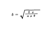
ここで、δは表皮深さを示し、図1に示す値となる。
従って薄膜のインピーダンスは
Z = Rdc (d / 2δ)+j ωLi(2 δ/ d )
となる。
ここで薄膜の厚さはd=2aとし、また、幅W、長さlとすると薄膜のインピーダンスは図2に示すものとなる。
ここで表皮深さδは図1で示すところであるので、薄膜のインピーダンスZは透磁率μθの関数となる。
【0014】
図3の(a)に示されるように薄膜のパターンの幅方向に一軸異方性が付与されているとき、磁化ベクトルは幅方向を向いて磁区構造は180°磁壁を持つ構造となる。ところで、この薄膜の長さ方向に高周波電流を流した場合、幅方向の高周波磁界が生じるが、180°磁壁の移動は渦電流制動により妨げられる。また、高周波磁界方向と磁化ベクトルの向きが同じ方向であるため回転磁化は起こりにくい。このため磁束の変化は少なく透磁率μθは小さい。
【0015】
一方、薄膜パターンの長さ方向に外部磁界Hexを印加すると磁化ベクトルの向きが幅方向から傾くので、高周波電流により生じる磁界により磁化ベクトルの回転が起こり(回転磁化)磁束の変化が生じるので透磁率μθが大きくなる。外部磁界Hexが膜パターンの異方性磁界Hkと同じになったとき透磁率μθは最大となり、このときインピーダンスZは最大となる。さらに外部磁界Hexが大きく(Hex>Hk)なると磁化ベクトルはHexに固定されるため磁化ベクトルの回転が抑制され、透磁率μθは小さくなっていき、それにともないインピーダンスZも小さくなっていく。
【0016】
これらの現象を回転磁化モデルに基づき図3の(b)を用いて検証する。H θ=0の場合回転角θ0は次式のエネルギー極小条件により定まる。
E0 = -Ku cos2(π/2 - θ0) - Ms Hex cos θ0 (3)
従って、
Hk = 2 Ku / Ms を用いて
θ0 = Hex / Hk
が得られる。
ここでHθによる回転角の変化 Δθ《θ0とすると幅方向の磁化変化分ΔMは次式で表せられる。
ΔM = Ms cosθ0 Δθ (4)
またHθによる項を含めた全エネルギーは次式で表せられる。

従ってHex<Hkでは磁界の増加とともに透磁率μθすなわちインピーダンスZが増加し、Hex=Hkで最大値をとった後、磁界の増加とともに減少することが示される。
また、磁化ベクトルが薄膜パターンの長さ方向に向いているときには外部磁界Hexによる幅方向の透磁率μθはほとんど変化しないのでMI効果は非常に小さくなる。
【0017】
ところで、図3の(a)に示した磁区構造は理想的なものであり、実際には単層の薄膜パターンの幅方向に一軸異方性を付与したときには幅方向に反磁界が生じ、その反磁界エネルギーを最小にするために磁区構造は図5に示すように磁化ベクトルが閉じた状態になる。この磁区構造をとることにより磁性体薄膜の内部磁化エネルギーは最小になり安定する。
【0018】
しかし、前述したように、磁化ベクトルが薄膜パターンの長さ方向に向いているときには外部磁界Hexによる幅方向の透磁率μθはほとんど変化しないのでMI効果は非常に小さくなる。つまり、図5に示す90°磁区の部分のMI効果は非常に小さいものであり、薄膜全体のMI効果を小さくしている。
【0019】
図6に示すように、幅方向に一軸異方性を付与し、かつ、中間に非磁性膜を挿入し磁性薄膜を2層にすることにより、静磁結合により上下の磁性膜の磁化ベクトルが結合し閉じた状態になる。この状態により薄膜の内部磁化エネルギーは最小となり安定化する。また、2層構造とした薄膜は180°磁区のみにより構成されるようになり、そのMI効果は単層膜に比べて大きくなる。
【0020】
図6に示される磁気インピーダンス素子の磁性膜はCoZrNb、FeSiB 、CoFeB 等のアモルファススパッタ膜、NiFeスパッタ膜等の軟磁性膜が用いられる。たとえば、NiFeスパッタ膜を用いた例を説明する。非磁性・絶縁性基板上にNiFeスパッタ膜を約2.5μmの厚さだけ成膜し、さらに、Ti等の非磁性膜を約10nm成膜し、最後にNiFeスパッタ膜を約2.5μmの厚さだけ成膜した。その後、所定の磁気コア形状のフォトレジストパターンを該薄膜上に形成し、該フォトレジストパターンをエッチング用マスクとして用い、イオンミーリング等のエッチング手段によりエッチングする。そして、フォトレジストパターンを有機溶剤等により除去することにより磁気インピーダンス素子を作製した。
【0021】
このときの非磁性膜の厚さは上下の磁性膜の交換結合を遮断できる厚さである必要があり、その厚さは10nm程度以上あれば良い。さらに、MI素子は表皮効果の透磁率依存性を用いているため、中間の非磁性膜にはTi、Ta、Cu、Al、Au、Ag、Pt等の導電性のある薄膜を用いることが望ましい。なお、これを絶縁薄膜で形成する場合は、積層された磁性膜の両方の端部を、両端側でそれぞれ互いに電気的に接続して、積層された磁性膜を電気的に並列接続させる。
【0022】
また、上下の磁性膜の磁化ベクトルが結合し全体の内部磁気エネルギーを最小にするためには、上下の磁性膜の磁化の総量を等しくする必要がある。この条件として、上層の磁性膜の磁化をMs1 、厚みをt1、下層の磁性膜の磁化をMs2 、厚みをt2とすると、Ms1 ×t1=Ms2 ×t2を満たすことが必要となる。
【0023】
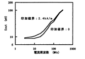
図7はTiを中間膜として用いNiFeスパッタ膜約2.5μm×2層の構造で作製した薄膜磁気インピーダンス素子に、素子の長さ方向に0および2.4kA/mの外部磁界(Hex)を印加したときのセンサ両端電極E(E=Z*I)の通電電流周波数特性である。Hex=0のときと、Hex=2.4kA/mのときのEの差ΔEは通電電流の周波数20MHz付近で最大であった。
【0024】
図8は本発明によるNiFeの2層薄膜磁気インピーダンス素子(2.5μm×2層)に通電電流周波数を20MHz(10mA)一定としたときのインピーダンスの変化率の印加磁界(Hex)依存性を示したものである。比較としてNiFe単層薄膜磁気インピーダンス素子(5μm)の特性を併記する。印加磁界を大きくしていくとインピーダンスの変化率ΔZ/Z0は大きくなり、素子の異方性磁界HkのところでΔZ/Z0は最大となり、さらにHex>HkではΔZ/Z0は小さくなっていく。これらの結果は前述の理論式で示した特性となった。また、インピーダンスの変化率は単層膜磁気インピーダンス素子の75%に対して2層膜磁気インピーダンス素子は90%と大きい値であった。このとき、単位印加磁界あたりのインピーダンスの変化量(磁界感度)はHex=1.6kA/m前後で最大となり0.08%/(A/m)の磁界感度を示した。
【0025】
また、本発明に関する薄膜磁気インピーダンス素子の作製方法としての他の実施例をあげる。所定の薄膜磁気コアの反転形状を薄い金属板に作製し、その金属板をスパッタマスクとして用い非磁性基板をマスクし、NiFeスパッタ膜を約2.5μmの厚さ、Ti等の非磁性膜を約10nmの厚さ、さらにNiFeスパッタ膜を約2.5μmの厚さだけ成膜し、磁気インピーダンス素子を作製する方法もある。
【0026】
NiFe、CoFe、NiFeP 、FeNiP 、FeCoP 、FeNiCoP 、CoB 、NiCoB 、FeNiCoB 、FeCoB 、CoFeNi等のめっき膜を磁性膜として用いた実施例を示す。まず、50nm程度の厚さのNiFeスパッタ膜をめっき用のシード層とするために形成する。そのシード層の上に所定のコイル形状の反転パターンのフォトレジストパターンを形成し、フォトレジストパターンの間にNiFeめっきを約2.5μmの厚さだけ埋め込む。つぎに、Cuなどの非磁性金属を約10nmめっき法にて堆積させる。さらに、その上にNiFeめっきを約2.5μmの厚さだけ埋め込む。その後、フォトレジストパターンを有機溶剤等により除去し、NiFeめっき膜のシード層をエッチングにより除去することにより磁気インピーダンス素子形成される。CoFeNi等のめっき膜を薄膜磁気コアとして用いたときも同様のプロセスで作製する。
【0027】
また、上記のいずれの方法で作製した薄膜磁気コアも、作製した後、回転磁場中、および静止磁場中で熱処理を行うと磁気特性の向上がはかれる。
【0028】
3層以上の多層膜において、つまり非磁性薄膜を介してn層(n≧3)積層されており、膜の間の非磁性膜が電気伝導体であり、また、それぞれ偶数番目の磁性膜の厚みと磁化の大きさの積の総和が、それぞれ奇数番目の磁性膜の厚みと磁化の大きさの積の総和におおむね等しい場合にそれぞれの層の磁性膜の磁化ベクトルは静磁結合をし、こ薄膜の内部磁化エネルギーは最小となり安定化する。また、この条件で多層構造とした薄膜は180°磁区のみにより構成されるようになり、そのMI効果は単層膜に比べて大きくなる。
【0029】
図9は3層構造の場合の実施例であり、このとき、最上層の磁性膜の磁化をMs1 、厚みをt1、第2層の磁性膜の磁化をMs2 、厚みをt2、最下層の磁性膜の磁化をMs3 、厚みをt3、とすると、Ms1 ×t1+Ms3 ×t3=Ms2 ×t2を満たすときそれぞれの磁性層の磁化ベクトルは静磁結合し、薄膜は180°磁区のみにより構成されるようになる。
【0030】
図10は4層構造の場合の実施の形態であり、このとき、最上層の磁性膜の磁化を Ms1、厚みをt1、第2層の磁性膜の磁化をMs2 、厚みをt2、第3層の磁性膜の磁化をMs3 、厚みをt3、第4層の磁性膜の磁化をMs4 、厚みをt4とすると、Ms1 ×t1+Ms3 ×t3=Ms2 ×t2+Ms4 ×t4を満たすときそれぞれの磁性層の磁化ベクトルは静磁結合し、薄膜は180°磁区のみにより構成されるようになる。
【0031】
また、図示はしていないが、n層構造の場合、最上層の磁性膜の磁化をMs1 、厚みをt1、第2層の磁性膜の磁化をMs2 、厚みをt2、……… 第n 層の磁性膜の磁化をMsn 、厚みをtn、とすると、偶数番目の磁性膜の厚みと磁化の大きさの積の総和が、それぞれ奇数番目の磁性膜の厚みと磁化の大きさの積の総和におおむね等しい条件を満たすとき、それぞれの磁性層の磁化ベクトルは静磁結合し、薄膜は180°磁区のみにより構成されるようになる。
【0032】
つぎに、2層薄膜磁気インピーダンス素子を用いて作製した薄膜磁気インピーダンス素子の特性について述べる。図11は本発明の実施の形態に用いられる薄膜磁気インピーダンス(MI)素子の構造を模式的に示した正面図、図12は図11のA−B線に沿って切断した断面図であり、図13は図11のC−D線に沿って切断した断面図である。実際の薄膜MIセンサ全体は薄膜セラミックス板、ガラス板のような板状体の上に形成されているが、図11ではこれを省略して示している。図11、図12及び図13において、1は平面形状が長方形の薄板状に形成された薄膜磁気コアであるMIセンサ板である。このMIセンサ板としての薄膜磁気コアの形状は、幅20μm、厚さ5μm、長さ500μmである。該MIセンサ板1の周囲には、絶縁物層2、3を介して、バイアスコイル4と負帰還コイル5が同一方向に且つ交互に巻回されている。図には正確に示してはいないが、これらコイルの巻数は、それぞれ20ターンである。バイアス用、負帰還用コイルを同一面上に交互に薄膜磁気コアに巻き回わす構造により磁気コアの各部位に均等にバイアス磁界、および負帰還磁界を加えることができ磁気センサとしての感度特性の直線性が向上する。バイアスコイル4の両端には、バイアスコイル端子6、7が接続され、負帰還コイル5の両端には、負帰還コイル端子8、9が接続されている。MIセンサ板1の両端には、MIセンサ端子10、11が接続されている。これら端子はAu金属薄膜から成り、先端の巾広部は、外部配線用のパッドとなる。なお、12は、MIセンサ全体を覆う絶縁保護膜である。
【0033】
薄膜磁気インピーダンス素子を磁気センサとして用いるときは最大感度のところに動作点を持ってくることによりセンサ感度を向上することができる。このため、バイアスコイルに電流を流すことによりバイアス磁界を加え動作点を変えることができ、1.6kA/mのバイアス磁界を薄膜コイルにを用いて磁気コアに印加することにより印加磁界0のところに磁界感度が最大になるようにした。
【0034】
一方、バイアスコイルを用いて印加磁界0に最大感度を持ってくるように動作点を移動した場合、磁界に対するインピーダンスの変化(出力の変化)の直線性はあまり良くないものとなる。この直線性を改善する方法として出力信号をフィードバックし負帰還コイルを用いて磁界に対する出力の非直線性を補正するだけの磁界を薄膜磁気コアに負帰還磁界として加えることにより出力信号を補正し直線性を得る方法がとられる。図14にリニア磁界MIセンサの出力検出部の電子回路のブロック図を示す。この回路により動作点を最大感度の点に移動し、出力信号をフィードバックし、薄膜コアに負帰還磁界を加え感度特性の直線性を高めている。
【0035】
図15は図14の回路を用いてバイアスコイル磁界1.6kA/m、負帰還率50%の負帰還をかけたときの印加磁界に対する出力電圧の関係を示したものである。ここで通電電流の周波数は20MHzであり出力の増幅度は500倍である。図に示すように±240A/mの測定磁界内で優れた直線性を示し、かつ、10-4A/mの磁界分解能を示した。これらの結果はリニア磁界センサとして良好な特性である。
【0036】
以上、本発明を上述の実施の形態により説明したが、本発明の主旨の範囲内で種々の変形や応用が可能であり、これらの変形や応用を本発明の範囲から排除するものではない。
【0037】
【発明の効果】
以上詳細に説明したように、本願の請求項1乃至9に係る発明では、薄膜磁気インピーダンス素子において、中間に非磁性膜を挿入し磁性薄膜を2層にすることにより、静磁結合により上下の磁性膜の磁化ベクトルが結合し閉じた状態にせしめ、この状態により薄膜の内部磁化エネルギーを最小とし、また、2層構造とした薄膜は180°磁区のみにより構成されるようになり、そのMI効果は単層膜に比べて大きくなる。これらのことから高感度の磁気インピーダンス素子を提供できる。
【図面の簡単な説明】
【図1】図1は、表皮深さδを表す方程式図である。
【図2】図2は、薄膜MI素子のインピーダンスを表す方程式図である。
【図3】図3は、薄膜MI素子の磁気コア部の磁区構造モデル図である。
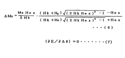
【図4】図4は、ΔM0の値を示す方程式図である。
【図5】図5は、本発明の一実施形態の磁気コア部の磁区構造モデル図である。
【図6】図6は、本発明の他の実施形態の磁気コア部の磁区構造モデル図である。
【図7】図7は、薄膜MI素子の通電電流周波数特性図である。
【図8】図8は、薄膜MI素子の印加磁界に対するインピーダンス変化率を示す特性図である。
【図9】図9は、本発明のもう一つ他の実施形態の磁気コア部の磁区構造モデル図である。
【図10】図10は、本発明のさらにもう一つ他の実施形態の磁気コア部の磁区構造モデル図である。
【図11】図11は、本発明に用いる薄膜磁気インピーダンス素子の構造を模式的に示した正面図である。
【図12】図12は、図1のA−B線に沿って切断した断面図である。
【図13】図13は、図1のC−D線に沿って切断した断面図である。
【図14】図14は、本発明に係る薄膜MI素子を用いた磁気センサの出力検出部の回路ブロック図である。
【図15】図15は、図14の回路における印加磁界に対するセンサ出力を示す特性図である。
【図16】図16は、磁性線からなるMI素子を用いた従来の磁気センサの回路ブロック図である。
【図17】図17は、図16に示す磁性線のインピーダンス変化の印加磁界依存性を示した特性図である。
【符号の説明】
1・・・・・MIセンサ板
2・・・・・絶縁物層
3・・・・・絶縁物層
4・・・・・バイアスコイル
5・・・・・負帰還コイル
6・・・・・バイアスコイル端子
7・・・・・バイアスコイル端子
8・・・・・負帰還コイル端子
9・・・・・負帰還コイル端子
10・・・・・MIセンサ端子
11・・・・・MIセンサ端子
12・・・・・絶縁保護膜
20・・・・・非磁性基板[0001]
BACKGROUND OF THE INVENTION
The present invention relates to a magnetic sensor, and more particularly to a high-sensitivity magnetic sensor using a thin film magneto-impedance element.
[0002]
[Prior art]
With the recent rapid development of information equipment and measurement / control equipment, there is an increasing demand for small, low-cost, high-sensitivity, high-speed response magnetic sensors. For example, hard disk drives for computer external storage devices have been improved in performance from bulk-type induction magnetic heads to thin film magnetic heads and magnetoresistive effect (MR) heads. As the number of magnetic poles of the magnet ring increases, a magnetic sensor capable of detecting a weak surface magnetic flux with high sensitivity is required in place of a conventionally used magnetoresistive effect (MR) sensor. There is also a growing demand for high-sensitivity magnetic sensors that can be used for nondestructive inspection and banknote inspection.
[0003]
Typical magnetic detection elements currently used include an inductive reproducing magnetic head, a magnetoresistive effect (MR) element, a fluxgate sensor, and a Hall element. Recently, a high-sensitivity magnetic sensor using the magneto-impedance effect of an amorphous wire has been proposed (see JP-A-6-176930, JP-A-7-181239, JP-A-7-333305), A high-sensitivity magnetic sensor using the magnetic impedance effect of a magnetic thin film has also been proposed (see Japanese Patent Application Laid-Open No. 8-75835, Journal of Applied Magnetics Society of Japan, vol. 20, 553 (1996)).
[0004]
The induction type reproducing magnetic head requires a coil winding, so that the magnetic head itself becomes large, and if the size is reduced, the relative speed between the magnetic head and the medium is lowered, and the detection sensitivity is remarkably lowered. On the other hand, a magnetoresistive effect (MR) element using a ferromagnetic film has been used. The MR element detects not the time change of the magnetic flux but the magnetic flux itself, and the miniaturization of the magnetic head has been promoted. However, the current MR element has a change rate of about 2%, and even an MR element using a spin valve element has a small change rate of an electric resistance of 6% or less and a resistance change of several%. The external magnetic field required to obtain the value is as large as 1600 A / m or more. Therefore, the magnetoresistive sensitivity is a low sensitivity of 0.001% / (A / m) or less. Recently, a giant magnetoresistance effect (GMR) using an artificial lattice having a magnetoresistance change rate of several tens of percent has been found. However, in order to obtain a resistance change of several tens of percent, an external magnetic field of tens of thousands of A / m is required, and it has not been put into practical use as a magnetic sensor.
[0005]
The conventional fluxgate sensor, which is a high-sensitivity magnetic sensor, measures magnetism by utilizing the fact that the symmetric BH characteristics of high-permeability magnetic cores such as ferrite and permalloy are changed by an external magnetic field. And high directivity of ± 1 °. However, a large magnetic core is required to increase detection sensitivity, and it is difficult to reduce the overall size of the sensor, and power consumption is high.
[0006]
A magnetic field sensor using a Hall element utilizes a phenomenon in which, when a magnetic field is applied perpendicularly to the plane of current flow, an electric field is generated in a direction perpendicular to both the current and applied magnetic fields, and an electromotive force is induced in the Hall element. It is a sensor. Although the Hall element is advantageous in terms of cost, it has low magnetic field detection sensitivity, and since it is composed of a semiconductor such as Si or GaAs, electrons or holes are scattered by scattering due to thermal oscillation of the lattice in the semiconductor against temperature changes. Has the disadvantage that the temperature characteristics of the magnetic field sensitivity are poor.
[0007]
As described in JP-A-6-176930, JP-A-7-181239, and JP-A-7-333305, a magneto-impedance element has been proposed to achieve a significant improvement in magnetic field sensitivity. This magneto-impedance element is a magneto-impedance element whose basic principle is to detect only a voltage with respect to a time change of a circumferential magnetic flux generated by applying a time-varying current to a magnetic wire as a change caused by an externally applied magnetic field. FIG. 16 shows an example of the magneto-impedance element. As this magnetic wire, an amorphous wire (wire subjected to tension annealing after drawing) having a diameter of about 30 μm with zero magnetostriction such as (FeCoSiB) is used, and FIG. 17 shows the applied magnetic field dependence of the impedance change of the wire. It is. Even if a wire with a minute dimension of about 1 mm in length is applied with a high frequency current of about 1 MHz, the amplitude of the voltage of the wire changes with a high sensitivity of about 0.1% / (A / m), which is 100 times or more that of the MR element.
[0008]
[Problems to be solved by the invention]
As a magnetic sensor, there is a demand for a high-sensitivity magnetic sensor that is small, low-cost, excellent in output linearity with respect to the detected magnetic field, and excellent in temperature characteristics. A magnetic sensor that uses the magneto-impedance effect of amorphous wire is a highly sensitive magnetic field. The detection characteristics are shown. In addition, in the ones disclosed in Japanese Patent Laid-Open Nos. 6-176930 and 6-347490, the linearity of the applied magnetic field dependency of the impedance change is improved by applying a bias magnetic field, and the amorphous wire is negatively affected. By winding a feedback coil and applying negative current by applying a current proportional to the voltage across the amorphous wire to the coil, a magnetic sensor with excellent linearity and invariable magnetic field detection sensitivity to changes in temperature of the sensor section can be obtained. Shown that you can offer.
[0009]
However, since this high-sensitivity magneto-impedance element is made of an amorphous wire having a diameter of about 30 μm, it is not suitable for fine processing, and it has been difficult to provide an ultra-small magnetic detection element. In addition, both the bias coil and the negative feedback coil have to be manufactured by winding a thin copper wire, and there is a limit to downsizing, and there is a problem in productivity.
[0010]
On the other hand, as an attempt to reduce the size, Japanese Patent Application Laid-Open No. 8-75935 proposes a magnetic impedance element using a magnetic thin film to reduce the size of the element. The inventors have proposed a small magneto-impedance element having a bias coil and a negative feedback coil by three-dimensionally winding a thin film coil around a thin film magnetic core in Japanese Patent Application No. 9-269084. However, in any of these inventions, the magnetic film has a single layer structure.
[0011]
Although details will be described in the embodiment, the magnetic domain structure shown in FIG. 3A is an ideal one. Actually, when uniaxial anisotropy is given in the width direction of the single-layer thin film pattern, the width direction In order to minimize the demagnetizing field energy, the magnetic domain structure has a magnetization vector closed as shown in FIG. However, since the magnetic permeability μθ in the width direction due to Hex hardly changes when the magnetization vector is oriented in the length direction of the thin film pattern, the MI effect becomes very small. That is, the MI effect in the 90 ° magnetic domain portion shown in FIG. 5 is very small, and the MI effect of the entire thin film is reduced.
The present invention has been made in view of the above circumstances, and provides a high-sensitivity magnetic sensor that is small in size, low in cost, and excellent in sensitivity characteristics with respect to a detection magnetic field.
[0012]
In order to achieve the above-described object of the present invention, according to one aspect of the present invention, a non-magnetic substrate, a thin film magnetic core formed on the substrate, and both ends in the longitudinal direction of the thin film magnetic core are provided. In the magneto-impedance element having the first electrode and the second electrode formed, the thin film magnetic core has a plurality of magnetic films stacked with a nonmagnetic thin film interposed therebetween, and the stacked magnetic The present invention provides a magnetoimpedance element characterized in that the thickness of the film is uneven.
Moreover, according to one aspect of the present invention, a substrate made of a non-magnetic material, a thin film magnetic core formed on the substrate, a first electrode and a second electrode provided at both ends in the longitudinal direction of the thin film magnetic core The thin film magnetic core has a plurality of magnetic films stacked with a nonmagnetic thin film interposed therebetween, and each of the odd-numbered magnetic films among the plurality of magnetic films. Provided is a magneto-impedance element characterized in that the total amount of the product of the thickness of the magnetic film and the magnitude of magnetization is substantially equal to the total amount of the product of the thickness and the magnitude of magnetization of each even-numbered magnetic film It is.
Moreover, according to one aspect of the present invention, a substrate made of a non-magnetic material, a thin film magnetic core formed on the substrate, a first electrode and a second electrode provided at both ends in the longitudinal direction of the thin film magnetic core A bias coil and a negative feedback coil that are alternately wound with an insulator interposed around the thin film magnetic core, the thin film magnetic core being non-magnetic A magneto-impedance element having a plurality of magnetic films stacked with a thin film interposed therebetween is provided.
According to another aspect of the present invention, there is provided a magneto-impedance element, wherein the non-magnetic thin film interposed between the magnetic films is an electric conductor.
Also, according to one aspect of the present invention, the nonmagnetic thin film interposed between the magnetic films is an insulator, and both ends of the laminated magnetic film are electrically connected to each other at both ends. A magneto-impedance element is provided.
Further, according to one aspect of the present invention, the magnetic film constituting the thin film magnetic core is formed of a plated film of NiFe, CoFe, NiFeP, FeNiP, FeCoP, FeNiCoP, CoB, NiCoB, FeNiCoB, FeCoB, CoFeNi. A magneto-impedance element is provided.
According to another aspect of the present invention, there is provided a magneto-impedance element, wherein the magnetic film constituting the thin film magnetic core is formed of an amorphous sputtered film of CoZrNb, FeSiB, or CoSiB. is there.
According to another aspect of the present invention, there is provided a magnetic impedance element wherein the magnetic film constituting the thin film magnetic core is formed of a NiFe sputtered film.
[0013]
DETAILED DESCRIPTION OF THE INVENTION
Hereinafter, an embodiment of the present invention will be described with reference to the drawings.
The magneto-impedance effect (MI effect) is a phenomenon in which when a high-frequency magnetic material is energized with a high-frequency current, the impedance between both ends is changed by an external magnetic field applied in the energizing direction. That is, the impedance Z due to the internal inductance component Li of the magnetic material and the resistance component Rw that increases with the current frequency f by the skin effect.
Z = Rw (μθ) + j ωLi (μθ) (1)
However, it is because it changes as a function of the magnetic permeability μ in the width direction of the magnetic material, which changes by applying a magnetic field from the outside.
In the case of a thin film, the resistance Rw of the thin film in the high frequency region (film thickness d >> 2δ) where the skin effect is remarkable is defined as the DC resistance is Rdc.
Rw = Rdc (d / 2 δ)
It can be expressed as.
On the other hand, if d >> 2δ, the inductance is
L = Li (2 δ / d)
It can be expressed as.
Here, δ represents the skin depth, which is the value shown in FIG.
Therefore, the impedance of the thin film is
Z = Rdc (d / 2δ) + jωLi (2δ / d)
It becomes.
Here, if the thickness of the thin film is d = 2a, and if the width is W and the length is 1, the impedance of the thin film is as shown in FIG.
Here, since the skin depth δ is as shown in FIG. 1, the impedance Z of the thin film is a function of the permeability μθ.
[0014]
As shown in FIG. 3A, when uniaxial anisotropy is imparted in the width direction of the thin film pattern, the magnetization vector faces in the width direction, and the magnetic domain structure has a 180 ° domain wall. By the way, when a high-frequency current is passed in the length direction of this thin film, a high-frequency magnetic field is generated in the width direction, but the movement of the 180 ° domain wall is hindered by eddy current braking. Further, since the direction of the high-frequency magnetic field and the direction of the magnetization vector are the same, rotational magnetization is unlikely to occur. For this reason, the change in magnetic flux is small and the permeability μθ is small.
[0015]
On the other hand, when the external magnetic field Hex is applied in the length direction of the thin film pattern, the direction of the magnetization vector is tilted from the width direction. Therefore, the magnetization vector is rotated by the magnetic field generated by the high-frequency current (rotational magnetization), and the magnetic flux is changed. μθ increases. When the external magnetic field Hex becomes the same as the anisotropic magnetic field Hk of the film pattern, the magnetic permeability μθ becomes maximum, and at this time, the impedance Z becomes maximum. Further, when the external magnetic field Hex increases (Hex> Hk), the magnetization vector is fixed to Hex, so that the rotation of the magnetization vector is suppressed, the permeability μθ decreases, and the impedance Z decreases accordingly.
[0016]
These phenomena are verified using FIG. 3B based on the rotational magnetization model. When Hθ = 0, the rotation angle θ0 is determined by the energy minimum condition of the following equation.
E0 = -Ku cos2 (π / 2-θ0)-Ms Hex cos θ0 (3)
Therefore,
Θk = Hex / Hk using Hk = 2 Ku / Ms
Is obtained.
Here, if the change in rotation angle due to Hθ is Δθ << θ0, the magnetization change ΔM in the width direction is expressed by the following equation.
ΔM = Ms cosθ0 Δθ (4)
The total energy including the term due to Hθ is expressed by the following equation.
Therefore, it is shown that when Hex <Hk, the magnetic permeability μθ, that is, the impedance Z increases as the magnetic field increases, and decreases as the magnetic field increases after taking the maximum value when Hex = Hk.
Further, when the magnetization vector is oriented in the length direction of the thin film pattern, the MI effect is very small because the permeability μθ in the width direction by the external magnetic field Hex hardly changes.
[0017]
By the way, the magnetic domain structure shown in FIG. 3 (a) is ideal. Actually, when uniaxial anisotropy is given in the width direction of the single-layer thin film pattern, a demagnetizing field is generated in the width direction. In order to minimize the demagnetizing field energy, the magnetic domain structure is in a state in which the magnetization vector is closed as shown in FIG. By taking this magnetic domain structure, the internal magnetization energy of the magnetic thin film is minimized and stabilized.
[0018]
However, as described above, when the magnetization vector is oriented in the length direction of the thin film pattern, the magnetic permeability μθ in the width direction by the external magnetic field Hex hardly changes, so the MI effect becomes very small. That is, the MI effect in the 90 ° magnetic domain portion shown in FIG. 5 is very small, and the MI effect of the entire thin film is reduced.
[0019]
As shown in FIG. 6, by giving uniaxial anisotropy in the width direction and inserting a non-magnetic film in the middle to form two magnetic thin films, the magnetization vectors of the upper and lower magnetic films can be obtained by magnetostatic coupling. Combined and closed. In this state, the internal magnetization energy of the thin film is minimized and stabilized. In addition, a thin film having a two-layer structure is configured only by a 180 ° magnetic domain, and its MI effect is larger than that of a single-layer film.
[0020]
As the magnetic film of the magneto-impedance element shown in FIG. 6, an amorphous sputtered film such as CoZrNb, FeSiB, or CoFeB, or a soft magnetic film such as a NiFe sputtered film is used. For example, an example using a NiFe sputtered film will be described. A NiFe sputtered film with a thickness of about 2.5 μm is formed on a nonmagnetic / insulating substrate, and a nonmagnetic film such as Ti is formed with a thickness of about 10 nm. Finally, a NiFe sputtered film with a thickness of about 2.5 μm is formed. Only the thickness was formed. Thereafter, a photoresist pattern having a predetermined magnetic core shape is formed on the thin film, and the photoresist pattern is used as an etching mask and is etched by an etching means such as ion milling. Then, the magnetoimpedance element was produced by removing the photoresist pattern with an organic solvent or the like.
[0021]
The thickness of the nonmagnetic film at this time needs to be a thickness that can block the exchange coupling between the upper and lower magnetic films, and the thickness should be about 10 nm or more. Furthermore, since the MI element uses the magnetic permeability dependence of the skin effect, it is desirable to use a conductive thin film such as Ti, Ta, Cu, Al, Au, Ag, and Pt as the intermediate nonmagnetic film. . When this is formed of an insulating thin film, both ends of the laminated magnetic films are electrically connected to each other at both ends, and the laminated magnetic films are electrically connected in parallel.
[0022]
Further, in order to combine the magnetization vectors of the upper and lower magnetic films to minimize the total internal magnetic energy, it is necessary to make the total amount of magnetization of the upper and lower magnetic films equal. As this condition, if the magnetization of the upper magnetic film is Ms1, the thickness is t1, the magnetization of the lower magnetic film is Ms2, and the thickness is t2, it is necessary to satisfy Ms1 × t1 = Ms2 × t2.
[0023]
FIG. 7 shows a thin film magneto-impedance element manufactured with a NiFe sputtered film of about 2.5 μm × 2 layers using Ti as an intermediate film, and an external magnetic field (Hex) of 0 and 2.4 kA / m in the length direction of the element. It is an energization current frequency characteristic of sensor both-ends electrode E (E = Z * I) when applying. The difference ΔE in E when Hex = 0 and Hex = 2.4 kA / m was the maximum near the frequency of the applied current of 20 MHz.
[0024]
FIG. 8 shows the applied magnetic field (Hex) dependence of the rate of change in impedance when the current carrying frequency is constant at 20 MHz (10 mA) in the NiFe two-layer thin film magnetoimpedance element (2.5 μm × 2 layers) according to the present invention. It is a thing. For comparison, the characteristics of a NiFe single-layer thin film magneto-impedance element (5 μm) are also shown. As the applied magnetic field is increased, the impedance change rate ΔZ / Z0 is increased, ΔZ / Z0 is maximized at the anisotropic magnetic field Hk of the element, and ΔZ / Z0 is decreased when Hex> Hk. These results were the characteristics shown by the above theoretical formula. The rate of change in impedance was as high as 90% for the double-layer film magnetic impedance element compared to 75% for the single-layer film magnetic impedance element. At this time, the amount of change in the impedance per unit applied magnetic field (magnetic field sensitivity) was maximum at around Hex = 1.6 kA / m, indicating a magnetic field sensitivity of 0.08% / (A / m).
[0025]
Another embodiment of a method for producing a thin film magneto-impedance element according to the present invention will be given. A reverse shape of a predetermined thin-film magnetic core is produced on a thin metal plate, the metal plate is used as a sputtering mask, a nonmagnetic substrate is masked, a NiFe sputtered film is about 2.5 μm thick, a nonmagnetic film such as Ti There is also a method in which a magneto-impedance element is fabricated by forming a NiFe sputtered film with a thickness of about 10 nm and a thickness of about 2.5 μm.
[0026]
An example is shown in which a plating film such as NiFe, CoFe, NiFeP, FeNiP, FeCoP, FeNiCoP, CoB, NiCoB, FeNiCoB, FeCoB, and CoFeNi is used as a magnetic film. First, a NiFe sputtered film having a thickness of about 50 nm is formed to serve as a seed layer for plating. A photoresist pattern having an inverted pattern having a predetermined coil shape is formed on the seed layer, and NiFe plating is embedded between the photoresist patterns to a thickness of about 2.5 μm. Next, a nonmagnetic metal such as Cu is deposited by about 10 nm plating. Further, NiFe plating is embedded thereon with a thickness of about 2.5 μm. Thereafter, the photoresist pattern is removed with an organic solvent or the like, and the seed layer of the NiFe plating film is removed by etching to form a magneto-impedance element. The same process is used when a plated film such as CoFeNi is used as the thin film magnetic core.
[0027]
In addition, when a thin film magnetic core manufactured by any of the above methods is manufactured and then subjected to heat treatment in a rotating magnetic field and in a static magnetic field, the magnetic properties are improved.
[0028]
In a multilayer film of three or more layers, that is, n layers (n ≧ 3) are laminated via a nonmagnetic thin film, the nonmagnetic film between the films is an electric conductor, and each of the even-numbered magnetic films When the sum of the product of the thickness and the magnitude of magnetization is approximately equal to the sum of the products of the thickness and the magnitude of magnetization of the odd-numbered magnetic films, the magnetization vectors of the magnetic films of the respective layers are magnetostatically coupled, The internal magnetization energy of this thin film is minimized and stabilized. In addition, a thin film having a multilayer structure under these conditions is composed of only 180 ° magnetic domains, and the MI effect is larger than that of a single layer film.
[0029]
FIG. 9 shows an embodiment in the case of a three-layer structure. At this time, the magnetization of the uppermost magnetic film is Ms1, the thickness is t1, the magnetization of the second magnetic film is Ms2, the thickness is t2, and the lowermost magnetic film is magnetic. When the magnetization of the film is Ms3 and the thickness is t3, when Ms1 × t1 + Ms3 × t3 = Ms2 × t2 is satisfied, the magnetization vector of each magnetic layer is magnetostatically coupled, and the thin film is composed only of 180 ° magnetic domains Become.
[0030]
FIG. 10 shows an embodiment in the case of a four-layer structure. At this time, the magnetization of the uppermost magnetic film is Ms1, the thickness is t1, the magnetization of the second magnetic film is Ms2, the thickness is t2, and the third layer. If the magnetization of the magnetic film is Ms3, the thickness is t3, the magnetization of the fourth magnetic film is Ms4, and the thickness is t4, the magnetization vector of each magnetic layer when Ms1 × t1 + Ms3 × t3 = Ms2 × t2 + Ms4 × t4 is satisfied Are magnetostatically coupled, and the thin film is composed only of 180 ° magnetic domains.
[0031]
Although not shown, in the case of the n-layer structure, the magnetization of the uppermost magnetic film is Ms1, the thickness is t1, the magnetization of the second magnetic film is Ms2, the thickness is t2,... If the magnetization of the magnetic film is Msn and the thickness is tn, the sum of the products of the even-numbered magnetic film thickness and the magnetization size is the sum of the product of the odd-numbered magnetic film thickness and the magnetization size, respectively. When almost equal conditions are satisfied, the magnetization vectors of the respective magnetic layers are magnetostatically coupled, and the thin film is composed of only 180 ° magnetic domains.
[0032]
Next, the characteristics of a thin film magneto-impedance element fabricated using a two-layer thin film magneto-impedance element will be described. FIG. 11 is a front view schematically showing the structure of a thin film magneto-impedance (MI) element used in the embodiment of the present invention. FIG. 12 is a cross-sectional view taken along the line AB of FIG. 13 is a cross-sectional view taken along the line CD in FIG. The entire actual thin film MI sensor is formed on a plate-like body such as a thin film ceramic plate or glass plate, but this is omitted in FIG. 11, 12, and 13,
[0033]
When a thin film magneto-impedance element is used as a magnetic sensor, the sensitivity of the sensor can be improved by bringing the operating point to the maximum sensitivity. For this reason, by applying a current to the bias coil, a bias magnetic field can be applied to change the operating point. By applying a bias magnetic field of 1.6 kA / m to the magnetic core using a thin film coil, the applied magnetic field is zero. The magnetic field sensitivity was maximized.
[0034]
On the other hand, when the operating point is moved so as to bring the maximum sensitivity to the applied
[0035]
FIG. 15 shows the relationship of the output voltage to the applied magnetic field when negative feedback with a bias coil magnetic field of 1.6 kA / m and a negative feedback rate of 50% is applied using the circuit of FIG. Here, the frequency of the energization current is 20 MHz, and the amplification factor of the output is 500 times. As shown in the figure, it showed excellent linearity in a measured magnetic field of ± 240 A / m and a magnetic field resolution of 10 −4 A / m. These results are good characteristics as a linear magnetic field sensor.
[0036]
As mentioned above, although this invention was demonstrated by the above-mentioned embodiment, various deformation | transformation and application are possible within the range of the main point of this invention, and these deformation | transformation and application are not excluded from the scope of the present invention.
[0037]
【The invention's effect】
As described above in detail, in the inventions according to
[Brief description of the drawings]
FIG. 1 is an equation diagram representing skin depth δ.
FIG. 2 is an equation diagram showing the impedance of a thin film MI element.
FIG. 3 is a magnetic domain structure model diagram of a magnetic core portion of a thin film MI element.
FIG. 4 is an equation diagram showing a value of ΔM0.
FIG. 5 is a magnetic domain structure model diagram of a magnetic core part according to an embodiment of the present invention.
FIG. 6 is a magnetic domain structure model diagram of a magnetic core part according to another embodiment of the present invention.
FIG. 7 is a diagram of current-current frequency characteristics of the thin film MI element.
FIG. 8 is a characteristic diagram showing an impedance change rate with respect to an applied magnetic field of the thin film MI element.
FIG. 9 is a magnetic domain structure model diagram of a magnetic core part according to another embodiment of the present invention.
FIG. 10 is a magnetic domain structure model diagram of a magnetic core portion according to still another embodiment of the present invention.
FIG. 11 is a front view schematically showing the structure of a thin-film magnetoimpedance element used in the present invention.
12 is a cross-sectional view taken along the line AB in FIG. 1. FIG.
13 is a cross-sectional view taken along line CD in FIG. 1. FIG.
FIG. 14 is a circuit block diagram of an output detection unit of a magnetic sensor using a thin film MI element according to the present invention.
15 is a characteristic diagram showing sensor output with respect to an applied magnetic field in the circuit of FIG.
FIG. 16 is a circuit block diagram of a conventional magnetic sensor using an MI element made of a magnetic wire.
FIG. 17 is a characteristic diagram showing the applied magnetic field dependence of the impedance change of the magnetic wire shown in FIG. 16;
[Explanation of symbols]
DESCRIPTION OF
Claims (8)
前記薄膜磁気コアは、間に非磁性薄膜を挟んで積層される複数の磁性膜を有し、
前記積層された磁性膜の厚みが不揃いであることを特徴とする磁気インピーダンス素子。In a magneto-impedance element having a substrate made of a non-magnetic material, a thin film magnetic core formed on the substrate, and a first electrode and a second electrode provided at both longitudinal ends of the thin film magnetic core,
The thin film magnetic core has a plurality of magnetic films stacked with a nonmagnetic thin film interposed therebetween,
A magneto-impedance element, wherein the laminated magnetic films are uneven in thickness.
前記薄膜磁気コアは、間に非磁性薄膜を挟んで積層される複数の磁性膜を有し、
前記複数枚の磁性膜のうち、奇数番目のそれぞれの磁性膜の厚みと磁化の大きさの積の合計量と、偶数番目のそれぞれの磁性膜の厚みと磁化の大きさの積の合計量がおおむね等しいことを特徴とする磁気インピーダンス素子。In a magneto-impedance element having a substrate made of a non-magnetic material, a thin film magnetic core formed on the substrate, and a first electrode and a second electrode provided at both longitudinal ends of the thin film magnetic core,
The thin film magnetic core has a plurality of magnetic films stacked with a nonmagnetic thin film interposed therebetween,
Of the plurality of magnetic films, the total amount of the product of the thickness of each odd-numbered magnetic film and the magnitude of magnetization and the total amount of the product of the thickness of each even-numbered magnetic film and the magnitude of magnetization are A magneto-impedance element characterized by being substantially equal.
前記薄膜磁気コアの周囲に絶縁体を媒介して交互に巻回されるバイアスコイルおよび負帰還コイルを備え、
前記薄膜磁気コアは、間に非磁性薄膜を挟んで積層される複数の磁性膜を有することを特徴とする磁気インピーダンス素子。In a magneto-impedance element having a substrate made of a non-magnetic material, a thin film magnetic core formed on the substrate, and a first electrode and a second electrode provided at both longitudinal ends of the thin film magnetic core,
A bias coil and a negative feedback coil that are alternately wound around an insulator around the thin film magnetic core;
The thin film magnetic core has a plurality of magnetic films stacked with a nonmagnetic thin film interposed therebetween, wherein the magnetoimpedance element is characterized in that:
Priority Applications (3)
| Application Number | Priority Date | Filing Date | Title |
|---|---|---|---|
| JP22176698A JP3676579B2 (en) | 1998-08-05 | 1998-08-05 | Magneto-impedance element |
| US09/366,547 US6472868B1 (en) | 1998-08-05 | 1999-08-04 | Magnetic impedance element having at least two thin film-magnetic cores |
| US10/231,169 US6650112B2 (en) | 1998-08-05 | 2002-08-30 | Magnetics impedance element having a thin film magnetics core |
Applications Claiming Priority (1)
| Application Number | Priority Date | Filing Date | Title |
|---|---|---|---|
| JP22176698A JP3676579B2 (en) | 1998-08-05 | 1998-08-05 | Magneto-impedance element |
Publications (2)
| Publication Number | Publication Date |
|---|---|
| JP2000055995A JP2000055995A (en) | 2000-02-25 |
| JP3676579B2 true JP3676579B2 (en) | 2005-07-27 |
Family
ID=16771875
Family Applications (1)
| Application Number | Title | Priority Date | Filing Date |
|---|---|---|---|
| JP22176698A Expired - Fee Related JP3676579B2 (en) | 1998-08-05 | 1998-08-05 | Magneto-impedance element |
Country Status (1)
| Country | Link |
|---|---|
| JP (1) | JP3676579B2 (en) |
Cited By (1)
| Publication number | Priority date | Publication date | Assignee | Title |
|---|---|---|---|---|
| CN109085523A (en) * | 2018-07-23 | 2018-12-25 | 中国科学院深圳先进技术研究院 | Suppressing method, device, equipment and the medium of cerebrospinal fluid signal in vascular wall imaging |
Families Citing this family (5)
| Publication number | Priority date | Publication date | Assignee | Title |
|---|---|---|---|---|
| JP2001119081A (en) * | 1999-08-09 | 2001-04-27 | Alps Electric Co Ltd | Magnetic impedance effect element and manufacturing method therefor |
| JP3882895B2 (en) * | 2001-12-14 | 2007-02-21 | スタンレー電気株式会社 | Crossed MI element |
| US7609478B2 (en) * | 2006-03-28 | 2009-10-27 | Seagate Technology Llc | Magnetic writer pole with a graded magnetic moment |
| JP4893367B2 (en) * | 2006-03-31 | 2012-03-07 | Tdk株式会社 | Thin film magnetic device |
| JP6549821B2 (en) * | 2014-07-04 | 2019-07-24 | ローム株式会社 | Semiconductor device |
-
1998
- 1998-08-05 JP JP22176698A patent/JP3676579B2/en not_active Expired - Fee Related
Cited By (2)
| Publication number | Priority date | Publication date | Assignee | Title |
|---|---|---|---|---|
| CN109085523A (en) * | 2018-07-23 | 2018-12-25 | 中国科学院深圳先进技术研究院 | Suppressing method, device, equipment and the medium of cerebrospinal fluid signal in vascular wall imaging |
| CN109085523B (en) * | 2018-07-23 | 2020-05-22 | 中国科学院深圳先进技术研究院 | Method, device, equipment and medium for inhibiting cerebrospinal fluid signals in vascular wall imaging |
Also Published As
| Publication number | Publication date |
|---|---|
| JP2000055995A (en) | 2000-02-25 |
Similar Documents
| Publication | Publication Date | Title |
|---|---|---|
| JP3022023B2 (en) | Magnetic recording / reproducing device | |
| JP2008197089A (en) | Magnetic sensor element and method for manufacturing the same | |
| US7145331B2 (en) | Magnetic sensor having a closed magnetic path formed by soft magnetic films | |
| US6650112B2 (en) | Magnetics impedance element having a thin film magnetics core | |
| JP3341237B2 (en) | Magnetic sensor element | |
| JP4047955B2 (en) | Magnetic impedance sensor | |
| KR100270148B1 (en) | Magnetoresistive head and the manufacturing method | |
| US6307708B1 (en) | Exchange coupling film having a plurality of local magnetic regions, magnetic sensor having the exchange coupling film, and magnetic head having the same | |
| JP3360168B2 (en) | Magnetic impedance element | |
| JP3676579B2 (en) | Magneto-impedance element | |
| JP4418986B2 (en) | Magnetic field detection element and magnetic field detection method using the same | |
| Fry et al. | Off-diagonal magnetoimpedance in NiFe-Au-NiFe layered film and its application to linear magnetic sensors | |
| JP4026050B2 (en) | Magnetic field detection element | |
| CN115128519A (en) | Magnetic sensor | |
| EP3851864B1 (en) | Magnetic sensor and current sensor | |
| JP4291455B2 (en) | Magnetic field sensor | |
| US6154348A (en) | Magnetoresistive head and method of initialization having a non-planar anti-ferromagnetic layer | |
| JP2003130932A (en) | Magnetic field detecting device | |
| JP3523834B2 (en) | Magnetic field sensor and magnetic field sensing system | |
| JP4034661B2 (en) | Guide sensor resistance value measuring method and thin film magnetic head manufacturing method | |
| JP3845695B2 (en) | Magnetic resonance type magnetic field detection element | |
| JP4474835B2 (en) | Magneto-impedance element | |
| JPH09106913A (en) | Magnetoelectric transducer | |
| JP3360172B2 (en) | Magnetic impedance head module | |
| JPH1183967A (en) | Method, system and element for detection of magnetic field |
Legal Events
| Date | Code | Title | Description |
|---|---|---|---|
| A977 | Report on retrieval |
Free format text: JAPANESE INTERMEDIATE CODE: A971007 Effective date: 20040802 |
|
| RD03 | Notification of appointment of power of attorney |
Free format text: JAPANESE INTERMEDIATE CODE: A7423 Effective date: 20041006 |
|
| A131 | Notification of reasons for refusal |
Free format text: JAPANESE INTERMEDIATE CODE: A131 Effective date: 20041217 |
|
| A521 | Request for written amendment filed |
Free format text: JAPANESE INTERMEDIATE CODE: A523 Effective date: 20050215 |
|
| TRDD | Decision of grant or rejection written | ||
| A01 | Written decision to grant a patent or to grant a registration (utility model) |
Free format text: JAPANESE INTERMEDIATE CODE: A01 Effective date: 20050426 |
|
| A61 | First payment of annual fees (during grant procedure) |
Free format text: JAPANESE INTERMEDIATE CODE: A61 Effective date: 20050428 |
|
| R150 | Certificate of patent or registration of utility model |
Free format text: JAPANESE INTERMEDIATE CODE: R150 |
|
| FPAY | Renewal fee payment (event date is renewal date of database) |
Free format text: PAYMENT UNTIL: 20090513 Year of fee payment: 4 |
|
| FPAY | Renewal fee payment (event date is renewal date of database) |
Free format text: PAYMENT UNTIL: 20090513 Year of fee payment: 4 |
|
| FPAY | Renewal fee payment (event date is renewal date of database) |
Free format text: PAYMENT UNTIL: 20100513 Year of fee payment: 5 |
|
| FPAY | Renewal fee payment (event date is renewal date of database) |
Free format text: PAYMENT UNTIL: 20110513 Year of fee payment: 6 |
|
| FPAY | Renewal fee payment (event date is renewal date of database) |
Free format text: PAYMENT UNTIL: 20110513 Year of fee payment: 6 |
|
| FPAY | Renewal fee payment (event date is renewal date of database) |
Free format text: PAYMENT UNTIL: 20120513 Year of fee payment: 7 |
|
| FPAY | Renewal fee payment (event date is renewal date of database) |
Free format text: PAYMENT UNTIL: 20130513 Year of fee payment: 8 |
|
| FPAY | Renewal fee payment (event date is renewal date of database) |
Free format text: PAYMENT UNTIL: 20140513 Year of fee payment: 9 |
|
| R250 | Receipt of annual fees |
Free format text: JAPANESE INTERMEDIATE CODE: R250 |
|
| LAPS | Cancellation because of no payment of annual fees |