JP3568183B2 - Variable transmission band method and apparatus for orthogonal frequency division multiplex modulation - Google Patents
Variable transmission band method and apparatus for orthogonal frequency division multiplex modulation Download PDFInfo
- Publication number
- JP3568183B2 JP3568183B2 JP01403398A JP1403398A JP3568183B2 JP 3568183 B2 JP3568183 B2 JP 3568183B2 JP 01403398 A JP01403398 A JP 01403398A JP 1403398 A JP1403398 A JP 1403398A JP 3568183 B2 JP3568183 B2 JP 3568183B2
- Authority
- JP
- Japan
- Prior art keywords
- clock
- unit
- transmission
- signal
- clock rate
- Prior art date
- Legal status (The legal status is an assumption and is not a legal conclusion. Google has not performed a legal analysis and makes no representation as to the accuracy of the status listed.)
- Expired - Fee Related
Links
Images


Description
【0001】
【発明の属する技術分野】
本発明は、直交周波数分割多重変調方式のディジタル伝送装置に関する。
【0002】
【従来の技術】
近年、ヨーロッパやアメリカ及び日本では、テレビジョン放送のディジタル化が検討されているが、その変調方式としては、OFDM(Orthogonal Frequency Division Multiplex)変調方式の採用が有力視されている。該OFDM変調方式は、マルチキャリア変調方式の一種で、多数のディジタル変調波を加え合わせたもので、このときの各キャリアの変調方式には、QPSK(Quadrature Phase Shift Keying)方式等が用いられる。
そして、このOFDM信号を式で表現すると、以下のように表される。
まず、各キャリアのQPSK信号をαk(t)とすると、これは式(1)で表せる。
αk(t)=ak(t)×cos(2πkft)+bk(t)×sin(2πkft) ……………(1)
ここで、kはキャリアの番号を示し、ak(t)、bk(t)は、k番目のキャリアのデータで、[−1]または[1]の値をとる。
次に、キャリアの本数をNとすると、OFDM信号はN本のキャリアの合成であり、これをβk(t)とすると、これは次の式(2)で表すことができる。
βk(t)=Σαk(t) ………………………………………………(2)
ここで、k=1〜N の値をとる。
【0003】
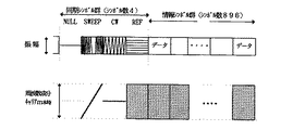
OFDM信号は、上記信号単位から構成される。 この信号単位シンボルは、例えば、有効サンプル1024サンプルのデータに、ガードインターバルデータ32サンプルを付加した、1056サンプルのシンボル396組に、4組の同期シンボルを付加した全400シンボルからなるフレームと呼ぶ、ストリーム単位の繰り返しで構成されている。
図6は、OFDM変復調装置の基本構成を示すブロック図である。
以下、OFDM変復調装置の構成と動作について、図7も用いて説明する。
連続的に入力されるデータDinは、レート変換部1でレート変換され、例えば400シンボルからなるフレーム周期毎に、後述の同期シンボル期間に対応する4シンボル期間と、各情報シンボルにおける、273から752サンプルまでの期間に対応する不要キャリア用ブランクを除いた期間に、データDiiとして出力される。
なおレート変換部1は、他の各部に同期シンボル期間の開始を示すFST信号をフレーム周期である400シンボル毎に出力する。
符号化部2Tは、入力データを符号化し、IとQの2軸にマッピングした符号化データRfとIfを出力する。
【0004】
IFFT(Inverse Fast Fourier Transform:逆フーリエ変換)部3Aは、符号化データRfとIfを周波数成分と見なし、1024サンプルからなる時間軸信号RとIに変換する。
ガード付加部3Bは、1024サンプルからなる信号RとIの開始期間波形の例えば最初の32サンプルの波形を1024サンプル後に付加し、合計1056サンプルの時間波形信号RgとIgを出力する。
同期シンボル挿入部5は、当該情報シンボルm個ごとに、予めメモリ等に記憶された、例えば4シンボルからなる同期シンボルの挿入された信号RsgとIsgを作成、出力する。
この信号は、直交変調処理部8にて直交変調され、図7の(b)に示すようなフレーム構成のOFDM変調波信号となり、送信側から受信側に送信される。
なお、クロック発振器11からのクロックCKは各部に供給される。
送信されたOFDM変調波は、受信側の直交復調処理部9にて、ベースバンドのOFDM信号に直交復調され、時間軸信号R’sgとI’sgとなり出力される。
当該信号R’sgとI’sgは、同期検出器4に入力され、ここで同期シンボル群が検出され、フレーム周期を表すFST’rパルスが各部に出力される。
また、時間軸信号R’sgとI’sgはFFT部3Cに入力され、時間波形信号から周波数成分信号R’fとI’fに変換される。
この信号R’fとI’fは、復号化部2Rで復号され、信号D’oが出力される。
そして、レート逆変換部7で連続したデータ信号Doutに変換後、出力される。
【0005】
次に、各部の詳細な構成、動作について述べる。
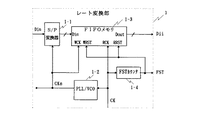
まず、レート変換部1の一例を図8に示し、説明する。
レート変換部1に入力されたクロックCKはPLL/VCO1−2に入力され、PLL/VCO1−2は、N/G倍の周波数のクロックCKmを出力する。
また、クロックCKは、FSTカウンタ1−4にも入力され、ここで送信側における処理のフレーム基準となるFSTパルスを発生、出力する。
なお、このFSTパルスは、FIFOメモリ1−3のWRST端子とRRST端子に入力され、書込みと読出しのリセットの基準になる。
そして、入力された連続データDinは、シリアル/パラレル(S/P)変換器1−1にてパラレル信号となり、FIFOメモリ1−3に入力され、ここで前述のごときブランク期間を有するデータ信号Dii(図7(a))が出力される。
【0006】
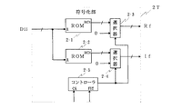
次に、符号化部2Tの一例を図9に示し、説明する。
上記レート変換部1出力の信号Diiは、マッピングROM2−1,2−2に入力され、I,Q軸の所定点の信号に変換される。 図7の(a)に示す、不要キャリアに相当する期間の信号は、選択器2−3,2−4にて”0”に置換され、前述の信号RfとIfが作成される。 この選択器2−3,2−4は、上記クロックCKとFSTパルスに基づきタイミングの定められたコントローラ2−5により制御される。
次に、IFFT変換部3Aの一例を図10に示し、説明する。
上記クロックCKとFSTパルスとでタイミングを決められたコントローラ3A−2により、ガード期間を含めたシンボル周期の信号を基準とし、上記入力信号RfとIfを、上記時間波形信号RとIに変換する。 これは、具体的には例えば、プレッシー社のPDSP16510等を用いれば実現できる。
【0007】
次に、ガード付加部3Bの一例を図11に示し、説明する。
ここに入力された上記信号RとIは、1024サンプルだけ信号を遅延する遅延器3B−1,3B−2と選択器3B−3,3B−4にそれぞれ入力され、各選択器3B−3,3B−4において、1から1024サンプル目までは遅延されない信号RとIが、1025サンプルから1056サンプル目までは遅延器3B−1,3B−2で1024サンプル遅延された信号が選択され、出力される。
その結果、出力される1シンボルが1056サンプルからなる信号Rg,Igは、1025サンプル目から1056サンプル目に1サンプルから32サンプル間の時間波形が付加される。 この選択器3B−3,3B−4は、上記クロックCKとFSTパルスとでタイミングを決められたコントローラ3B−5によって制御される。
次に、同期シンボル挿入部5の一例を図12に示し、説明する。
上記クロックCKとFSTパルスによってタイミングを決められたコントローラ5−5によって制御されるROM5−1,5−2は、前述の同期シンボル信号をFSTパルスに応じたタイミングで発生する。
同様に、クロックCKとFSTパルスとでタイミングを決められたコントローラ5−6により制御される選択器5−3,5−4は、上記ガード付加部3Bで作成されたガード付時間信号RgとIgの現段階では無信号期間である、4シンボル期間のみ、ROM5−1,5−2からの同期シンボル信号を選択して出力する。その結果、同期シンボル信号の挿入された、図7の(a)に示す時間波形信号RsgとIsgが出力される。
【0008】
ここで、図7の(b)に記載のNULLシンボルは、同期シンボル群の存在を大まかに見つけるためのもので、このシンボル期間は信号を一切出力しない。 また、SWEEPシンボルは、各シンボルの切り替わり点を正確に求めるためのものであり、1シンボル期間に伝送帯域の下限周波数から上限周波数に変化する波形からなる。
そして、直交変調処理部8のD/A変換器81において、上記時間波形信号の実数部信号Rsgと虚数部信号IsgのD/A変換を行ない、直交変調器82で実数部信号に対してはローカル発振器83からの周波数fcのキャリア信号で、一方、虚数部信号に対してはローカル発振器83の周波数fcのキャリア信号を90°移相した信号で直交変調し、これらの信号を合成しOFDM信号を得る。
【0009】
次に、受信側の構成、動作について説明する。
まず、前述伝送されたフレーム構成の信号が直交復調処理部9に入力される。ここでの処理は、送信側とは逆に、直交復調器91にて、電圧制御発振器93のキャリア信号で復調したものを実数部信号、90°移相したキャリア信号で復調した出力を虚数部信号として取り出すものである。 これら実数部、虚数部の各復調アナログ信号は、A/D変換器94にてディジタル信号に変換される。
次に、同期検出器4の一例を図13に示し、説明する。
上記直交復調されたディジタル信号R’sgとI’sgは、NULL終了検出器4−1とSWEEP演算部4−2とに入力される。
NULL終了検出器4−1は、フレーム構成のシンボル群の中から、無信号の期間であるNULLシンボルを検出し、同期シンボルの大まかな位置を検出し、NULL終了時点から図示しないタイマ回路にてSWEEPシンボル開始時期を推定してSWEEP期間フラグパルスを出力する。
SWEEP演算部4−2は、SWEEP期間フラグパルスを参照し、NULLシンボルの後に存在するSWEEPシンボルによって、各シンボルの正確な切り替わりタイミングを捜索する。具体的には、予めSWEEPシンボルのパターンを内蔵メモリに記憶しておき、入力されたOFDM信号と該メモリに記憶された信号を相関演算し、メモリの信号パターンとOFDM信号のパターンが一致した時点で、一致パルスをフレームカウンタ4−4のリセット端子に入力する。
【0010】
フレームカウンタ4−4は、カウント数がフレーム周期を構成する値、例えば422400(=1056×400)に到達すると、その値を0に戻すとともに、フレーム開始時期を示すFSTrパルスを出力し、再びカウントを開始する。
以後は、一定カウント、即ちフレーム開始点毎にFSTrパルスが出力され、フレーム開始時期を示す。 受信側では、このFSTrパルスをFFT部3C、復号化部2R、レート逆変換部7における開始タイミングとする。
FFT変換部5は、FSTrパルスを基にシンボルを区切り、フーリエ変換を行うことでOFDM復調を行い、上記周波数成分信号R’fとI’fを出力する。
復号化部2Rは、例えばROMテーブル手法にて、これら信号R’fとI’fを識別し、復号化信号D’oを算出する。
レート逆変換部7は、上記クロックCKrとFSTrパルスによって動作タイミングが決定され、レート変換部1の構成を反転(逆に)した構成である。
ところで、伝送されるOFDM信号の帯域幅は、ベースバンド信号Rsg,Isgの帯域の2倍となる。 ベースバンド信号Rsg,Isgの帯域は、IFFT部3Aに入力するキャリアに相当するデータに依存して決定される。
【0011】
ここで、IFFT部3Aの動作について、図14を使い説明する。
周波数成分である信号Rfは、周期1/Sのクロックに同期し順次入力される。
1番目のデータf0は、直流成分であるキャリア0の振幅レベルを決定する。2番目のデータf1は、周期1024/Sのキャリア1の振幅レベルを決定し、3番目のデータf2は、周期512/Sのキャリア2の振幅レベルを決定する。
このようにして入力された最高周波数成分がIFFT変換によって作成される時間波形の最高周波数、すなわち帯域幅を決定する。
なお、このようにして個別の振幅を決定されて変換作成された各キャリアは、これらが総加算されて、時間波形信号Rが作成される。
ただし、この時間波形信号Rは、計1024サンプルのデータから構成されており、各サンプルデータは周期1/Sのクロックに同期して出力される。即ち、キャリア1は、入力クロック周期の1024倍の周波数となる。
【0012】
【発明が解決しようとする課題】
以上説明した従来構成の伝送装置において、伝送帯域幅の変更を行なう場合、以下の部分の変更が必要となる。
1)伝送容量の変更に伴い、送信側のレート変換部1のPLL/VCO1−4のN/G特性。
2)送信側の符号化部2Tにおいて、不要キャリア振幅を0にするため置換する0の期間の変更をするコントローラ2−5の制御特性。
3)帯域変更に伴い、送信側の同期挿入部5において、SWEEPシンボルに対応する周波数パターンを記憶しているROM5−1,5−2のデータ。
4)受信側の同期検出器4のSWEEP演算部4−2の内蔵メモリに記憶されたSWEEPシンボルパターン。
5)受信側のレート逆変換部7のPLL/VCO特性。
このように従来の伝送装置では、伝送帯域幅を変更しようとしても、送信側と受信側の双方で変更しなければならない部分が多く、また、送信側で行った帯域可変処理に受信側が追随しないため、伝送帯域幅を容易に、かつ瞬時に変更することができない。
本発明はこれらの欠点を除去し、帯域幅の可変を容易に行える伝送システムの実現を目的とする。
【0013】
【課題を解決するための手段】
本発明は、上記目的を達成するため、送信側において各部に供給するクロックレートを変更し、受信側では、受信信号から検出した同期信号と受信側クロックを分周して作成したフレーム信号とを位相比較し、その結果により受信クロック発振部のクロック周波数を制御し、受信側で復調する帯域を送信側の帯域に自動追随させて伝送帯域を可変するようにしたものである。
即ち、送信側のIFFT変換において、n番目のデータfnは、n番目のキャリアの周期1024/(n・S)の振幅レベルを決定する。 ここで、IFFT変換部に供給されるクロックの周期を変更すれば、n番目のキャリアの周波数も変更される。伝送帯域幅は、発生するキャリアの最高周波数で決定される。
すなわち、帯域の可変が、クロックの周期を変更することにより実現できる。また、クロックの周期の変更でシンボル周期も変更され、このシンボル数で決定されるフレーム周期も変更される。
受信側では、受信信号から検出したNULLシンボルとSWEEPシンボルの周期、すなわち、送信側のフレーム周期と、フレームカウンタで定められているFSTr周期とを比較し、差分を解消するように、受信側クロックの周期を制御する。
これにより、送信側で行った帯域可変処置に自動追随する伝送システムを構築できる。
【0014】
【発明の実施の形態】
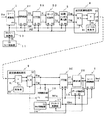
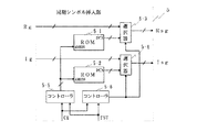
本発明の帯域可変伝送システムの一実施例の全体ブロック構成を図1に示し、説明する。
送信側において、クロック発振器11のクロック出力端子は、クロックレート変換部10に接続される。 クロックレート変換部10のクロック出力端子は、レート変換部1、符号化部2T、IFFT部3A、ガード付加部3B、同期シンボル挿入部5、直交変調処理部8の各クロック端子に接続される。
受信側において、同期検出器15の出力VCは、電圧制御クロック発振器12の端子VCに接続される。 同期検出器15の出力FSTrは、FFT部3C、レート逆変換部7のFST端子に接続される。 電圧制御クロック発振器12の出力CKrは、FFT部3C、レート逆変換部7、直交復調処理部9、同期検出器15のクロックCK端子に接続される。
【0015】
まず、送信側における帯域可変処理動作について説明する。
伝送帯域幅の変更を行う場合、クロックレート変換部10において、クロック発振器11からのクロックCKを、変更する帯域幅に応じたレートのクロックに変換する。 すなわち、クロックレート変換部10は、クロックCKのレートの(V/NR)倍したレートのクロックCKdを出力する。
ここで、レート変換部1から出力される前述のフレーム周期パルスFSTは、例えば、上記クロックCKdの1056×400カウント毎に出力されるため、クロックCKdとフレーム周期パルスFSTとを基準に動作する符号化部2T、IFFT部3A、ガード付加部3B、同期シンボル挿入部5、直交変調処理部8では、それぞれサンプルレートが(V/NR)倍となった出力データを、それぞれ(NR/V)倍の期間をかけて出力することになる。
また、レート変換部1内のPLL/VCO1−4(図8)は、入力するクロックレートが(V/NR)倍になるため、N/Gの比率のクロックCKmも(V/NR)倍となり、取り込まれるデータDinのレートも(V/NR)倍になる。
ここで、例えば、(V/NR)を1/2とした場合について説明する。
この場合、IFFT部3Aにおいて、サンプルクロックCKdが1/2になると各キャリア間隔は1/2に、またシンボル周期は2倍になる。
このとき、キャリアの本数を変更していないため、(V/NR)が1/2の本例の場合、帯域幅は、キャリア間隔×キャリア本数で決定され、半分となる。
即ち、クロックレートを(V/NR)倍にすることにより、帯域幅を(V/NR)倍に変更することができる。
【0016】
次に、受信側における帯域可変処理動作について説明する。
同期検出器15は、前述のようにして、入力された信号R’sgとI’sgから検出したNULL期間を基準としてSWEEPシンボルを探し、受信フレーム周期を示す一致パルスと位相比較してクロックCKrcの周波数を制御する。また、このクロックCKrcを、例えば1056×400カウントして作成したフレーム周期パルスFSTrcを出力する。
ここで、FFT部3C、レート逆変換部7は、このパルスFSTrcとクロックCKrcにより動作するため、送信側でのサンプルレートがV/NR倍されている場合、FSTrcパルスとの位相比較基準である一致パルスは、NR/V倍の周期であるから、このクロックCKrcが、通常時のV/NR倍の周波数にまで変更された場合に、FSTrcパルスと一致パルスの周期及び位相が合致する。
【0017】
図2に、この同期検出器15の具体的構成を示し、説明する。
入力される信号R’sgとI’sgは、NULL終了検出器15−1とSWEEP演算部15−2に入力される。 NULL終了検出器15−1出力であるSWEEP期間フラグパルスは、SWEEP演算部15−2のST端子に入力される。
NULL終了検出器15−1、SWEEP演算部15−2、フレームカウンタ15−4のCK端子には、クロックCKrcが入力される。
SWEEP演算部4−2の出力である一致パルスは、PLL15−3のR端子に入力される。
また、クロックCKrcを1056×400数えるフレームカウンタ15−4の出力FSTrcは、後段の回路およびPLL15−3のV端子に入力される。
PLL15−3は、V端子とR端子にそれぞれ入力されるパルスの位相に応じて電圧が変化する信号VCを出力する。
そして、電圧制御型のクロック発振器12は、同期検出器15から印加される上記信号VCの電圧の高低に応じて、即ち、送信側のクロックCKdのクロックレート変換に応じて、出力するクロックCKrcの周波数を上下させる。
以上説明した処理によって、受信側において用いるクロックCKrcとフレーム周期パルスFSTrcを、送信側において変更したクロックCKdとフレーム周期パルスFSTに追随させることができる。
【0018】
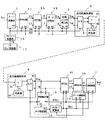
次に、本発明の帯域可変伝送システムの第2の実施例のブロック構成を図3に示し、上記図1と異なる部分を中心にして説明する。
受信側のクロック発振器16の出力クロックCKrcは、クロックレート変換部17に入力される。クロックレート変換部17の出力クロックCKrcは、FFT部3C、レート逆変換部7、データ確認部18のCK端子に接続される。
データ確認部18のFST端子には、同期検出器15のFSTrcパルスが入力され、D端子には復号化部2Rの出力D’oが入力される。
前述の如く、送信側で伝送帯域幅を、V/NR(例えば、1/2)にした場合、キャリア本数を変更しないため、キャリア間隔はV/NRになる。
ここで、受信側において、元々のクロックレートでFFT変換動作を行うと、即ち、キャリア間隔が1倍のままFFT変換を行うと、その結果として復号化部2Rから得られる出力D’oは、1本おきに”0”となる歯抜け状態となる。また、逆に送信側のクロックレートが1倍で、受信側がV/NR倍のクロックレートで動作すると、復号化部2Rから得られる出力D’oは、周波数の高い方のキャリアのデータが無い状態となってしまう。
そこで、データ確認部18にて、この出力D’oの状態を調べ、送信側におけるクロックレートの変更状態を確認する。
【0019】
そして、データ確認部18では、受信側におけるクロックレートが、送信側のクロックレート変更に対応するクロックレートになる様、クロックレート変換部17に対し、クロックレートの変更を指示する制御信号を出力する。
これにより、クロックレート変換部17は、受信側におけるクロックCKrcをデータ確認部18からの制御信号に基づき、送信側のクロックレート変更に対応したクロックレートに変更する。
ここで、送信側のクロックレート変換を、単純な1/2倍や1/3倍等とすることにより、受信側のデータ確認部18の確認動作において、誤検出することが少なくなる。
以上説明した構成によって、受信側において用いるクロックCKrcとフレーム周期パルスFSTrcを、送信側において変更したクロックCKdとフレーム周期パルスFSTに追随させることができる。
【0020】
次に、本発明の帯域可変伝送システムの第3の実施例のブロック構成を図4に示す。これは、図1の構成に、レート変換部17とデータ確認部18を追加した構成であり、動作説明を省略する。
ここで、クロックレート変換部10,17は、論理素子による分周動作のみにより、クロックレートを、1/2,1/3,1/4等に変える機能のみとする。これは、受信側の電圧制御型のクロック発振器12の周波数変化幅が狭い範囲でしか可変できない場合に、主に用いられる構成である。
次に、本発明を適用した帯域自動可変伝送システムの構成を図5に示す。
回線状態監視装置106は、使用する回線の電波使用状態を調べ、空き具合に応じて使用する周波数と使える帯域幅を決定するもので、切換制御信号S1を帯域可変変調装置101の制御端子に出力する。また、切換制御信号S2を周波数変換送信装置102の制御端子に出力する。
帯域可変変調装置101、周波数変換送信装置102は、図1、図3、図4の送信側の構成を大きくブロック化して示したもので、帯域可変変調装置101はレート変換部1〜同期シンボル挿入部5等に対応し、周波数変換送信装置102は、直交変調処理部8に対応する。いずれも、外部から切換コントロール可能な機能が付加されたものである。
また、帯域可変復調装置104は、キャリアの有無等の復調状態から切換制御信号S3を、周波数変換受信装置103に送る。
周波数変換受信装置103、帯域可変復調装置104は、図1、図3、図4の受信側の構成を大きくブロック化して示したもので、周波数変換受信装置103は直交復調処理部9に対応し、帯域可変復調装置104はFFT部3C〜レート逆変換部7等に対応するものである。
【0021】
以下、この動作について述べる。
まず、伝送開始に先立ち、送信側では、回線状態監視装置106により、使用回線の電波使用状態を調べ、回線の空き具合に応じて、使用する周波数と使える帯域幅を決定する。
そして、切換制御信号S1により使用する帯域幅を、切換制御信号S2により使用する周波数を、それぞれ帯域可変変調装置101、周波数変換送信装置102に指定する。
これにより、帯域可変変調装置101では、使用する帯域幅になるよう、前述のようなクロックレート変更が行われ、使用する帯域幅になる。 また、周波数変換送信装置102では、使用する周波数となるように、ローカル発振周波数が制御され、使用する周波数となる。 そして、使用する周波数、帯域幅となった送信信号が、受信側に送出される。
一方、受信側では、帯域可変復調装置104において、全てのキャリアが存在しない状態、キャリアの一部のみが存在する状態、予定したキャリアがおおよそ存在する状態のいずれであるかを判別し、対応する切換制御信号S3を周波数変換受信装置103に出力する。
周波数変換受信装置103では、この切換制御信号S3によって、受信周波数が切換えられ、送信側からの送信信号を受信できるようになる。
これら構成をとることで、空きチャネルを自動探索してその空き帯域に応じた伝送帯域幅でデータ伝送を行うシステムを構築できる。
【0022】
ここで、図15に、クロックレートを1倍とした場合のフレーム周期時間と、その際の周波数成分の関係を示す。 また、図16に、クロックレートを高めた場合のフレーム周期時間と、その際の周波数成分の関係を示す。
前述のように、クロックレートを1/2に下げればフレーム周期は2倍になるが、周波数帯域は1/2になる。
従って、図15の場合の1チャネル(ch)分の帯域を、図16の場合は、別個に利用することができる。
つまり、図5に示す伝送システムにおいて、送信および受信周波数を、1/2ch単位に変更できる周波数変換送信装置102と、周波数変換受信装置103とを組み合わせる。
これにより、1ch分の帯域を複数伝送に利用することができるようになり、限られた伝送帯域を有効に利用することができる。
【0023】
【発明の効果】
以上説明したように、本発明によれば、送信側にてクロックレートを変更することで帯域可変は可能となり、かつ、受信側はその変更に自動的に追尾する伝送システムを実現できる。
【図面の簡単な説明】
【図1】本発明のデータ伝送システムの全体構成を示すブロック図
【図2】本発明で用いる同期検出器15の構成を示すブロック図
【図3】本発明の他のデータ伝送システムの全体構成を示すブロック図
【図4】本発明の他のデータ伝送システムの全体構成を示すブロック図
【図5】本発明を適用した帯域自動可変伝送システムの全体構成を示すブロック図
【図6】従来のデータ伝送システムの全体構成を示すブロック図
【図7】本発明の各部の波形タイムチャートおよびフレーム構成波形図
【図8】レート変換部1の構成を示すブロック図
【図9】符号化部2Tの構成を示すブロック図
【図10】IFFT部3Aの構成を示すブロック図
【図11】ガード付加部3Bの構成を示すブロック図
【図12】同期シンボル挿入部5の構成を示すブロック図
【図13】同期検出器4の構成を示すブロック図
【図14】IFFT部3Aの動作を説明する図
【図15】クロックレート1倍の場合のフレーム周期時間と周波数成分の関係を示す図
【図16】クロックレートのアップ時のフレーム周期時間と周波数成分の関係を示す図
【符号の説明】
1:レート変換部、2T:符号化部、3A:IFFT部、3B:ガード付加部、5:同期シンボル挿入部、3C:FFT部、2R:復号化部、7:レート逆変換部、8:直交変調処理部、9:直交復調処理部、10,17:クロックレート変換部、11,12,16:クロック発振器、15:同期検出器、18:データ確認部、15−1:NULL終了検出器、15−2:SWEEP演算部、15−4:フレームカウンタ、15−3:PLL。[0001]
TECHNICAL FIELD OF THE INVENTION
The present invention relates to an orthogonal frequency division multiplex modulation digital transmission apparatus.
[0002]
[Prior art]
In recent years, digitization of television broadcasting has been studied in Europe, the United States, and Japan, and the adoption of an OFDM (Orthogonal Frequency Division Multiplex) modulation system is considered to be the most promising modulation system. The OFDM modulation system is a type of multi-carrier modulation system in which a large number of digitally modulated waves are added. At this time, a QPSK (Quadrature Phase Shift Keying) system or the like is used as a modulation system for each carrier.
When this OFDM signal is expressed by an equation, it is expressed as follows.
First, the QPSK signal of each carrier is set to α k Assuming (t), this can be expressed by equation (1).
α k (T) = a k (T) × cos (2πkft) + b k (T) × sin (2πkft) (1)
Here, k indicates a carrier number, and a k (T), b k (T) is the data of the k-th carrier and takes a value of [-1] or [1].
Next, assuming that the number of carriers is N, the OFDM signal is a combination of N carriers, which is represented by β k Assuming (t), this can be represented by the following equation (2).
β k (T) = Σα k (T) …………………………… (2)
Here, values of k = 1 to N are taken.
[0003]
An OFDM signal is composed of the above signal units. This signal unit symbol is referred to as, for example, a frame composed of 1024 valid sample data to which 32 pieces of guard interval data are added, 396 sets of 1056 sample symbols, and 4 sets of synchronization symbols added to all 400 symbols. It consists of repetitions in stream units.
FIG. 6 is a block diagram showing a basic configuration of the OFDM modem.
Hereinafter, the configuration and operation of the OFDM modem will be described with reference to FIG.
The continuously input data Din is rate-converted by the
Note that the
The
[0004]
An IFFT (Inverse Fast Fourier Transform)
The
The synchronization
This signal is quadrature-modulated by the quadrature
The clock CK from the clock oscillator 11 is supplied to each unit.
The transmitted OFDM modulated wave is orthogonally demodulated into a baseband OFDM signal by an orthogonal
The signals R'sg and I'sg are input to the
Further, the time axis signals R'sg and I'sg are input to the
The signals R'f and I'f are decoded by the
Then, after being converted into a continuous data signal Dout by the rate
[0005]
Next, the detailed configuration and operation of each unit will be described.
First, an example of the
The clock CK input to the
The clock CK is also input to the FST counter 1-4, where it generates and outputs an FST pulse that serves as a frame reference for processing on the transmission side.
The FST pulse is input to the WRST terminal and the RRST terminal of the FIFO memory 1-3, and serves as a reference for resetting writing and reading.
Then, the input continuous data Din is converted into a parallel signal by the serial / parallel (S / P) converter 1-1 and input to the FIFO memory 1-3. Here, the data signal Dii having the blank period as described above. (FIG. 7A) is output.
[0006]
Next, an example of the
The signal Dii output from the
Next, an example of the
The
[0007]
Next, an example of the
The signals R and I input here are input to
As a result, the output signals Rg and Ig each consisting of 1056 samples are added with a time waveform from 1 sample to 32 samples from the 1025th sample to the 1056th sample. The
Next, an example of the synchronization
The ROMs 5-1 and 5-2 controlled by the controller 5-5 whose timing is determined by the clock CK and the FST pulse generate the synchronization symbol signal at a timing corresponding to the FST pulse.
Similarly, the selectors 5-3 and 5-4 controlled by the controller 5-6 whose timing is determined by the clock CK and the FST pulse output the guarded time signals Rg and Ig generated by the
[0008]
Here, the NULL symbol shown in FIG. 7B is for roughly detecting the existence of a group of synchronization symbols, and does not output any signal during this symbol period. The SWEEP symbol is for accurately determining the switching point of each symbol, and has a waveform that changes from the lower limit frequency to the upper limit frequency of the transmission band in one symbol period.
Then, the D /
[0009]
Next, the configuration and operation of the receiving side will be described.
First, the transmitted frame-structured signal is input to the quadrature
Next, an example of the
The quadrature-demodulated digital signals R'sg and I'sg are input to the NULL end detector 4-1 and the SWEEP operation unit 4-2.
The NULL end detector 4-1 detects a NULL symbol, which is a period of no signal, from the symbol group of the frame structure, detects a rough position of the synchronization symbol, and uses a timer circuit (not shown) from the NULL end time point. A SWEEP symbol start time is estimated to output a SWEEP period flag pulse.
The SWEEP operation unit 4-2 refers to the SWEEP period flag pulse and searches for an accurate switching timing of each symbol by using the SWEEP symbol existing after the NULL symbol. More specifically, the pattern of the SWEEP symbol is stored in the built-in memory in advance, the input OFDM signal is correlated with the signal stored in the memory, and the correlation between the signal pattern of the memory and the pattern of the OFDM signal is determined. Input the coincidence pulse to the reset terminal of the frame counter 4-4.
[0010]
When the counted number reaches a value constituting the frame period, for example, 422400 (= 1056 × 400), the frame counter 4-4 returns the value to 0, outputs an FSTr pulse indicating a frame start time, and counts again. To start.
Thereafter, an FSTr pulse is output at a constant count, that is, at each frame start point, indicating the frame start time. On the receiving side, the FSTr pulse is used as a start timing in the
The
The
The operation of the rate
By the way, the bandwidth of the transmitted OFDM signal is twice the bandwidth of the baseband signals Rsg and Isg. The bands of the baseband signals Rsg and Isg are determined depending on the data corresponding to the carrier input to the
[0011]
Here, the operation of the
The signal Rf as a frequency component is sequentially input in synchronization with a clock having a period of 1 / S.
The first data f0 determines the amplitude level of
The highest frequency component thus input determines the highest frequency of the time waveform created by the IFFT conversion, that is, the bandwidth.
Note that the respective carriers that have been converted and created by determining the individual amplitudes in this way are added up to generate the time waveform signal R.
However, the time waveform signal R is composed of a total of 1024 samples of data, and each sample data is output in synchronization with a clock having a period of 1 / S. That is, the
[0012]
[Problems to be solved by the invention]
In the transmission device having the conventional configuration described above, when the transmission bandwidth is changed, the following changes are required.
1) N / G characteristics of the PLL / VCO 1-4 of the
2) Control characteristics of the controller 2-5 for changing the period of 0 to be replaced in order to reduce the unnecessary carrier amplitude to 0 in the
3) Data in the ROMs 5-1 and 5-2 storing frequency patterns corresponding to SWEEP symbols in the
4) The SWEEP symbol pattern stored in the internal memory of the SWEEP operation unit 4-2 of the
5) PLL / VCO characteristics of the
As described above, in the conventional transmission device, even if an attempt is made to change the transmission bandwidth, there are many parts that need to be changed on both the transmission side and the reception side, and the reception side does not follow the band variable processing performed on the transmission side. Therefore, the transmission bandwidth cannot be easily and instantaneously changed.
An object of the present invention is to eliminate these drawbacks and to realize a transmission system capable of easily changing the bandwidth.
[0013]
[Means for Solving the Problems]
In order to achieve the above object, the present invention changes the clock rate supplied to each unit on the transmitting side, and on the receiving side, converts the synchronization signal detected from the received signal and the frame signal generated by dividing the receiving side clock. The phase is compared, the clock frequency of the receiving clock oscillator is controlled based on the result, and the transmission band is varied by automatically following the band demodulated on the receiving side to the band on the transmitting side.
That is, in the IFFT conversion on the transmission side, the n-th data fn determines the amplitude level of the cycle 1024 / (n · S) of the n-th carrier. Here, if the period of the clock supplied to the IFFT conversion unit is changed, the frequency of the n-th carrier is also changed. The transmission bandwidth is determined by the highest frequency of the generated carrier.
That is, the band can be varied by changing the clock cycle. Further, the symbol period is changed by changing the clock period, and the frame period determined by the number of symbols is also changed.
On the receiving side, the period of the NULL symbol and the SWEEP symbol detected from the received signal, that is, the frame period on the transmitting side is compared with the FSTr period determined by the frame counter, and the clock on the receiving side is removed so as to eliminate the difference. Control the cycle of
This makes it possible to construct a transmission system that automatically follows the band variable procedure performed on the transmission side.
[0014]
BEST MODE FOR CARRYING OUT THE INVENTION
An overall block configuration of an embodiment of the variable bandwidth transmission system according to the present invention will be described with reference to FIG.
On the transmitting side, a clock output terminal of the clock oscillator 11 is connected to the
On the receiving side, the output VC of the
[0015]
First, the band variable processing operation on the transmitting side will be described.
When changing the transmission bandwidth, the
Here, since the above-described frame cycle pulse FST output from the
In the PLL / VCO 1-4 (FIG. 8) in the
Here, for example, a case where (V / NR) is set to 1/2 will be described.
In this case, in the
At this time, since the number of carriers is not changed, in the present example where (V / NR) is 2, the bandwidth is determined by the carrier interval × the number of carriers, and is halved.
That is, by increasing the clock rate by (V / NR) times, the bandwidth can be changed to (V / NR) times.
[0016]
Next, the band variable processing operation on the receiving side will be described.
As described above, the
Here, since the
[0017]
FIG. 2 shows a specific configuration of the
The input signals R'sg and I'sg are input to the NULL end detector 15-1 and the SWEEP operation unit 15-2. The SWEEP period flag pulse output from the null end detector 15-1 is input to the ST terminal of the SWEEP operation unit 15-2.
The clock CKrc is input to the CK terminals of the NULL end detector 15-1, the SWEEP operation unit 15-2, and the frame counter 15-4.
The coincidence pulse output from the SWEEP operation unit 4-2 is input to the R terminal of the PLL 15-3.
The output FSTrc of the frame counter 15-4 that counts the clock CKrc by 1056 × 400 is input to a circuit at the subsequent stage and the V terminal of the PLL 15-3.
The PLL 15-3 outputs a signal VC whose voltage changes according to the phases of the pulses input to the V terminal and the R terminal.
Then, the voltage controlled
By the processing described above, the clock CKrc and the frame cycle pulse FSTrc used on the receiving side can follow the clock CKd and the frame cycle pulse FST changed on the transmitting side.
[0018]
Next, FIG. 3 shows a block configuration of a band variable transmission system according to a second embodiment of the present invention, and a description will be given focusing on parts different from FIG.
The output clock CKrc of the
The FSTrc pulse of the
As described above, when the transmission bandwidth is set to V / NR (for example, 1/2) on the transmission side, the carrier interval is V / NR because the number of carriers is not changed.
Here, when the FFT conversion operation is performed at the original clock rate on the receiving side, that is, when the FFT conversion is performed with the carrier interval being 1, the output D′ o obtained from the
Therefore, the data check
[0019]
Then, the
Thereby, the clock
Here, by making the clock rate conversion on the transmission side simple 1/2 times, 1/3 times or the like, erroneous detection is reduced in the confirmation operation of the
With the configuration described above, the clock CKrc and the frame period pulse FSTrc used on the receiving side can follow the clock CKd and the frame period pulse FST changed on the transmitting side.
[0020]
Next, FIG. 4 shows a block configuration of a third embodiment of the variable bandwidth transmission system of the present invention. This is a configuration in which a
Here, the
Next, FIG. 5 shows a configuration of an automatic band variable transmission system to which the present invention is applied.
The line
The band
The variable-
The frequency
[0021]
Hereinafter, this operation will be described.
First, on the transmitting side, before starting transmission, the line
Then, the bandwidth used by the switching control signal S1 and the frequency used by the switching control signal S2 are specified to the variable
As a result, in the variable-
On the receiving side, on the other hand, the band
In the frequency
With these configurations, it is possible to construct a system for automatically searching for an empty channel and transmitting data with a transmission bandwidth corresponding to the empty band.
[0022]
Here, FIG. 15 shows the relationship between the frame cycle time when the clock rate is set to 1 and the frequency component at that time. FIG. 16 shows the relationship between the frame cycle time when the clock rate is increased and the frequency component at that time.
As described above, if the clock rate is reduced to 1 /, the frame period is doubled, but the frequency band is 1 /.
Therefore, the band for one channel (ch) in the case of FIG. 15 can be used separately in the case of FIG.
That is, in the transmission system shown in FIG. 5, the frequency
As a result, the band for one channel can be used for a plurality of transmissions, and the limited transmission band can be used effectively.
[0023]
【The invention's effect】
As described above, according to the present invention, by changing the clock rate on the transmitting side, it is possible to change the band, and the receiving side can realize a transmission system that automatically tracks the change.
[Brief description of the drawings]
FIG. 1 is a block diagram showing the overall configuration of a data transmission system according to the present invention.
FIG. 2 is a block diagram showing a configuration of a
FIG. 3 is a block diagram showing the overall configuration of another data transmission system of the present invention.
FIG. 4 is a block diagram showing the overall configuration of another data transmission system of the present invention.
FIG. 5 is a block diagram showing an overall configuration of an automatic band variable transmission system to which the present invention is applied;
FIG. 6 is a block diagram showing the overall configuration of a conventional data transmission system.
FIG. 7 is a waveform time chart and a frame configuration waveform diagram of each unit according to the present invention.
FIG. 8 is a block diagram showing a configuration of a
FIG. 9 is a block diagram showing a configuration of an
FIG. 10 is a block diagram showing a configuration of an
FIG. 11 is a block diagram showing a configuration of a
FIG. 12 is a block diagram showing a configuration of a synchronization
FIG. 13 is a block diagram showing a configuration of a
FIG. 14 is a diagram for explaining the operation of the
FIG. 15 is a diagram showing a relationship between a frame cycle time and a frequency component when the clock rate is 1 time.
FIG. 16 is a diagram showing a relationship between a frame cycle time and a frequency component when the clock rate is increased.
[Explanation of symbols]
1: Rate conversion unit, 2T: coding unit, 3A: IFFT unit, 3B: guard addition unit, 5: synchronization symbol insertion unit, 3C: FFT unit, 2R: decoding unit, 7: rate inverse conversion unit, 8: Quadrature modulation processing unit, 9: quadrature demodulation processing unit, 10, 17: clock rate conversion unit, 11, 12, 16: clock oscillator, 15: synchronization detector, 18: data confirmation unit, 15-1: NULL end detector , 15-2: SWEEP operation unit, 15-4: frame counter, 15-3: PLL.
Claims (4)
送信側では、送信側クロック発振器の出力をクロックレート変換して作成したクロックを、レート変換部、符号化部、IFFT部、ガード付加部、同期シンボル挿入部、直交変調処理部に供給する際、伝送帯域に応じてクロックレートを変更することで上記作成したクロックの周波数を切り換え、
受信側では、受信側クロック発振器の出力をクロックレート変換して作成したクロックと受信信号から検出した同期信号とに基づいて上記受信信号をFFT変換後、復号化処理し、該復号化処理により得られた出力データの状態に応じてクロックレートを変更することで上記作成したクロックの周波数を切り換え、
受信側で復調する伝送帯域を、送信側の上記伝送帯域に自動追随させることを特徴とする直交周波数分割多重方式の伝送帯域変更方法。In a transmission band changing method of an orthogonal frequency division multiplexing transmission device,
On the transmission side, when a clock created by clock rate conversion of the output of the transmission side clock oscillator is supplied to a rate conversion unit, an encoding unit, an IFFT unit, a guard addition unit, a synchronization symbol insertion unit, and a quadrature modulation processing unit, By changing the clock rate according to the transmission band, the frequency of the clock created above is switched,
On the receiving side, the received signal is subjected to FFT conversion based on a clock generated by converting the output of the receiving-side clock oscillator at a clock rate and a synchronization signal detected from the received signal, and then subjected to a decoding process. By changing the clock rate according to the state of the output data obtained, the frequency of the clock created above is switched,
A transmission band changing method of an orthogonal frequency division multiplexing method, wherein a transmission band demodulated on a receiving side is automatically made to follow the transmission band on the transmitting side.
送信側クロック発振器の出力をクロックレート変換して作成したクロックを、レート変換部、符号化部、IFFT部、ガード付加部、同期シンボル挿入部、直交変調処理部に供給するクロックレート変換部を送信装置に備え、
受信側クロック発振器の出力をクロックレート変換するクロックレート変換部と、該クロックレート変換部の出力と受信信号から検出した同期信号とに基づいて上記受信信号をFFT変換した後に復号化する信号処理部と、該信号処理部の出力データの状態に応じて上記クロックレート変換部を制御するデータ確認部を受信装置に備え、
受信側で復調する伝送帯域を、送信側の伝送帯域に自動追随させることを特徴とする直交周波数分割多重方式の伝送装置。In an orthogonal frequency division multiplexing transmission device,
It transmits the output of the transmission side clock oscillator created by clock rate conversion clock rate conversion unit, the encoding unit, IFFT unit, a guard addition section, synchronization symbol insertion section, the clock rate conversion unit is supplied to the orthogonal modulation processing unit In preparation for the device,
A clock rate conversion unit that converts the output of the clock oscillator on the receiving side into a clock rate, and a signal processing unit that performs FFT conversion on the reception signal based on the output of the clock rate conversion unit and a synchronization signal detected from the reception signal and then decodes the signal. And a receiving device including a data confirmation unit that controls the clock rate conversion unit according to a state of output data of the signal processing unit,
A transmission apparatus of an orthogonal frequency division multiplex system, wherein a transmission band demodulated on a reception side is automatically made to follow a transmission band on a transmission side.
上記送信装置に接続され、電波使用状態を調べることにより得られた空き伝送帯域に応じて伝送帯域幅を決める回線状態監視部を備え、上記空き伝送帯域に応じて決まった上記伝送帯域幅でデータ伝送を行うことを特徴とする直交周波数分割多重方式の伝送装置。 In the transmission apparatus of an orthogonal frequency division multiplexing according to claim 2,
A line state monitoring unit connected to the transmitting device and determining a transmission bandwidth according to an available transmission band obtained by checking a radio wave use state, wherein data is transmitted at the transmission bandwidth determined according to the available transmission band. An orthogonal frequency division multiplexing transmission device for performing transmission.
ここで用いる変調方式をQAM方式としたことを特徴とする直交周波数分割多重方式の伝送装置。 The transmission apparatus of the orthogonal frequency division multiplex system according to claim 2 or 3,
An orthogonal frequency division multiplexing transmission apparatus, wherein a modulation method used here is a QAM method.
Priority Applications (3)
| Application Number | Priority Date | Filing Date | Title |
|---|---|---|---|
| JP01403398A JP3568183B2 (en) | 1998-01-27 | 1998-01-27 | Variable transmission band method and apparatus for orthogonal frequency division multiplex modulation |
| EP99101093A EP0932284A3 (en) | 1998-01-27 | 1999-01-26 | Multicarrier transmission system, with modifiable bandwidth |
| US09/236,601 US6611493B1 (en) | 1998-01-27 | 1999-01-26 | Communication, transmission and receiving method and apparatus using orthogonal frequency division multiplexing modulation system |
Applications Claiming Priority (1)
| Application Number | Priority Date | Filing Date | Title |
|---|---|---|---|
| JP01403398A JP3568183B2 (en) | 1998-01-27 | 1998-01-27 | Variable transmission band method and apparatus for orthogonal frequency division multiplex modulation |
Publications (2)
| Publication Number | Publication Date |
|---|---|
| JPH11215093A JPH11215093A (en) | 1999-08-06 |
| JP3568183B2 true JP3568183B2 (en) | 2004-09-22 |
Family
ID=11849845
Family Applications (1)
| Application Number | Title | Priority Date | Filing Date |
|---|---|---|---|
| JP01403398A Expired - Fee Related JP3568183B2 (en) | 1998-01-27 | 1998-01-27 | Variable transmission band method and apparatus for orthogonal frequency division multiplex modulation |
Country Status (1)
| Country | Link |
|---|---|
| JP (1) | JP3568183B2 (en) |
Families Citing this family (4)
| Publication number | Priority date | Publication date | Assignee | Title |
|---|---|---|---|---|
| JP2003101506A (en) * | 2001-09-25 | 2003-04-04 | Sony Corp | Wireless communication apparatus and wireless communication method, wireless communication system, and channel assignment system |
| WO2004077712A1 (en) | 2003-02-28 | 2004-09-10 | Ntt Docomo, Inc. | Radio communication system and radio communication method |
| US9313067B2 (en) * | 2007-08-14 | 2016-04-12 | Qualcomm Incorporated | Multi-bandwidth communication system using a shared baseband processor |
| JP6155085B2 (en) * | 2012-09-28 | 2017-06-28 | 日本放送協会 | OFDM transmitter for wireless microphone, receiver, and transmission / reception system |
-
1998
- 1998-01-27 JP JP01403398A patent/JP3568183B2/en not_active Expired - Fee Related
Also Published As
| Publication number | Publication date |
|---|---|
| JPH11215093A (en) | 1999-08-06 |
Similar Documents
| Publication | Publication Date | Title |
|---|---|---|
| CN1309484B (en) | Sampling offset correction method and system and in quadrature frequency division multiplex receiver | |
| CN1293714C (en) | Local oscillator frequency correction in quadrature frequency-division multiplex system | |
| CN103973626B (en) | Low power remote transmitter | |
| US6192056B1 (en) | Demodulating apparatus and demodulating method | |
| EP0682426B1 (en) | OFDM transmitter and receiver | |
| US5761190A (en) | OFDM broadcast wave receiver | |
| US6064695A (en) | Spread spectrum communication system utilizing differential code shift keying | |
| US5657313A (en) | Signal transmitting apparatus and signal receiving apparatus using orthogonal frequency division multiplexing | |
| US6611493B1 (en) | Communication, transmission and receiving method and apparatus using orthogonal frequency division multiplexing modulation system | |
| JP4288777B2 (en) | Multi-carrier signal transmitter and multi-carrier signal receiver | |
| JP3568183B2 (en) | Variable transmission band method and apparatus for orthogonal frequency division multiplex modulation | |
| EP0991238B1 (en) | Generation and decoding of multi-carrier signal | |
| JP3568184B2 (en) | Orthogonal frequency division multiplexing modulation transmission band variable method and apparatus therefor | |
| JPH11331133A (en) | Two-way digital transmission method and device thereof | |
| JP3761397B2 (en) | Digital transmission system | |
| JP3580107B2 (en) | OFDM demodulator and method | |
| JP3636006B2 (en) | Digital transmission equipment | |
| JP3729481B2 (en) | Data transmission apparatus synchronization detection control method and apparatus | |
| JP2000068974A (en) | Ofdm receiver | |
| JP4142037B2 (en) | DIGITAL TRANSMISSION SYSTEM AND DIGITAL TRANSMISSION SYSTEM TRANSMISSION STATUS NOTIFICATION METHOD | |
| JP3651875B2 (en) | Data transmission device | |
| JP3770585B2 (en) | Digital transmission equipment | |
| JP4519371B2 (en) | Transmission device, transmission device, and reception device | |
| JP3518739B2 (en) | Orthogonal frequency division multiplex signal receiving apparatus and orthogonal frequency division multiplex signal receiving method | |
| JP3518764B2 (en) | Orthogonal frequency division multiplex signal receiving apparatus and orthogonal frequency division multiplex signal receiving method |
Legal Events
| Date | Code | Title | Description |
|---|---|---|---|
| A977 | Report on retrieval |
Free format text: JAPANESE INTERMEDIATE CODE: A971007 Effective date: 20040202 |
|
| A131 | Notification of reasons for refusal |
Free format text: JAPANESE INTERMEDIATE CODE: A131 Effective date: 20040315 |
|
| A521 | Written amendment |
Free format text: JAPANESE INTERMEDIATE CODE: A523 Effective date: 20040514 |
|
| TRDD | Decision of grant or rejection written | ||
| A01 | Written decision to grant a patent or to grant a registration (utility model) |
Free format text: JAPANESE INTERMEDIATE CODE: A01 Effective date: 20040614 |
|
| A61 | First payment of annual fees (during grant procedure) |
Free format text: JAPANESE INTERMEDIATE CODE: A61 Effective date: 20040614 |
|
| R150 | Certificate of patent or registration of utility model |
Free format text: JAPANESE INTERMEDIATE CODE: R150 |
|
| FPAY | Renewal fee payment (event date is renewal date of database) |
Free format text: PAYMENT UNTIL: 20090625 Year of fee payment: 5 |
|
| FPAY | Renewal fee payment (event date is renewal date of database) |
Free format text: PAYMENT UNTIL: 20100625 Year of fee payment: 6 |
|
| FPAY | Renewal fee payment (event date is renewal date of database) |
Free format text: PAYMENT UNTIL: 20110625 Year of fee payment: 7 |
|
| FPAY | Renewal fee payment (event date is renewal date of database) |
Free format text: PAYMENT UNTIL: 20120625 Year of fee payment: 8 |
|
| FPAY | Renewal fee payment (event date is renewal date of database) |
Free format text: PAYMENT UNTIL: 20130625 Year of fee payment: 9 |
|
| FPAY | Renewal fee payment (event date is renewal date of database) |
Free format text: PAYMENT UNTIL: 20140625 Year of fee payment: 10 |
|
| LAPS | Cancellation because of no payment of annual fees |