JP3112223U - Bullet ball machine - Google Patents

Bullet ball machine Download PDF

Info

Publication number
JP3112223U
JP3112223U JP2005002731U JP2005002731U JP3112223U JP 3112223 U JP3112223 U JP 3112223U JP 2005002731 U JP2005002731 U JP 2005002731U JP 2005002731 U JP2005002731 U JP 2005002731U JP 3112223 U JP3112223 U JP 3112223U
Authority
JP
Japan
Prior art keywords
control board
data
power
prize ball
game
Prior art date
Legal status (The legal status is an assumption and is not a legal conclusion. Google has not performed a legal analysis and makes no representation as to the accuracy of the status listed.)
Expired - Fee Related
Application number
JP2005002731U
Other languages
Japanese (ja)
Other versions
JP3112223U7 (en
Inventor
敏博 内ヶ島
隆寛 内ヶ島
正吾 巽
Original Assignee
株式会社高尾
Priority date (The priority date is an assumption and is not a legal conclusion. Google has not performed a legal analysis and makes no representation as to the accuracy of the date listed.)
Filing date
Publication date
Application filed by 株式会社高尾 filed Critical 株式会社高尾
Priority to JP2005002731U priority Critical patent/JP3112223U/en
Application granted granted Critical
Publication of JP3112223U publication Critical patent/JP3112223U/en
Publication of JP3112223U7 publication Critical patent/JP3112223U7/ja
Anticipated expiration legal-status Critical
Expired - Fee Related legal-status Critical Current

Links

Images

Abstract

【課題】ノイズや不正行為による賞球制御基板のデータクリアを防止する。
【解決手段】賞球制御基板は、電源基板の電源スイッチをオンすることによるリセットから予め定められた設定時間T1内に、データクリアコマンドを入力した場合には記憶保持手段により記憶されたデータをクリアし、予め定められた設定時間T1経過後にデータクリアコマンドを入力してもデータをクリアすることを禁止する。電源基板の電源スイッチをオンすることによりリセットされたときから予め定められた設定時間T2経過後から設定時間T1が経過するまでの間に、データクリアコマンドを入力した場合のみバックアップRAM69に記憶保持により記憶されたデータをクリアする。
【選択図】図22
To prevent data clear of a prize ball control board due to noise or fraud.
When a clear data command is input within a preset time T1 from a reset by turning on a power switch of a power supply board, the prize ball control board stores the data stored by the storage holding means. Clearing and prohibiting data clear even if a data clear command is input after a predetermined set time T1 has elapsed. Only when a data clear command is input during a period from when the preset time T2 elapses until the set time T1 elapses after being reset by turning on the power switch of the power supply board, the backup RAM 69 is stored and retained. Clear stored data.
[Selection] Figure 22

Description

本考案は弾球遊技機に関し、特に賞球制御基板の電源投入時の賞球に係るデータのクリアに関する。   The present invention relates to a ball game machine, and more particularly to clearing data related to a prize ball when a prize ball control board is powered on.

近年の弾球遊技機は、停電時にも遊技状態及び賞球データ等の遊技データを記憶保持し、停電復帰後には停電発生時のゲームから再開することが行われている。停電時に記憶保持された遊技データは、製造メーカから出荷時やパチンコホールでの営業開始時にはクリアする必要が生じる場合もあり、遊技データをクリアするデータクリアスイッチも備えられている。   In recent years, a ball game machine stores game data such as a game state and prize ball data even in the event of a power failure, and resumes from a game at the time of the power failure after a power failure. The game data stored and retained at the time of a power failure may need to be cleared at the time of shipment from the manufacturer or at the start of business in the pachinko hall, and a data clear switch for clearing the game data is also provided.

この遊技データは、パチンコ店の営業中はクリアされるべきデータではなく、また誤操作によりクリアされるべきデータでもない。
このための発明が種々が為されている。例えば、特許文献1と特許文献2に開示される発明では、電源基板にクリアスイッチが設けられているが、遊技データをクリアするという観点にたてば、遊技制御基板にデータクリアスイッチを設けるのが好適である。また、電源基板からのノイズや不正防止の観点からも遊技制御基板にデータクリアスイッチを設けるのが好適である。遊技制御基板にデータクリアスイッチを設けた発明は、特許文献1に開示されている(同文献1の図14、図23、図19)
This game data is not data that should be cleared during the operation of the pachinko parlor, and is not data that should be cleared due to an erroneous operation.
Various inventions for this purpose have been made. For example, in the inventions disclosed in Patent Document 1 and Patent Document 2, a clear switch is provided on the power supply board, but from the viewpoint of clearing game data, a data clear switch is provided on the game control board. Is preferred. In addition, it is preferable to provide a data clear switch on the game control board from the viewpoint of noise from the power supply board and fraud prevention. An invention in which a data clear switch is provided on a game control board is disclosed in Patent Document 1 (FIGS. 14, 23, and 19 of the same document 1).

ここで、遊技データは1回の操作で遊技制御基板及び賞球制御基板に記憶保持されたデータをクリアするほうが操作性の面で好適である(同文献1の図14、図23(a)及び(b))。   Here, it is more preferable in terms of operability to clear the game data stored in the game control board and the prize ball control board in one operation (FIGS. 14 and 23 (a) of the same document 1). And (b)).

電源投入時に遊技制御基板のデータクリアスイッチを押下し、遊技制御基板及び賞球制御基板に記憶保持されたデータを共にクリアする場合には、データクリアスイッチが押下されると遊技制御基板から賞球制御基板にデータクリアコマンドを出力する必要がある(同文献1の図23(a))。   When the data clear switch on the game control board is pressed when the power is turned on to clear both the data stored and held in the game control board and the prize ball control board, when the data clear switch is pressed, the game control board receives the prize ball. It is necessary to output a data clear command to the control board (FIG. 23 (a) of the document 1).

一方、データクリアスイッチと、電源スイッチの誤操作防止の観点から、特許文献2に開示される発明がなされている。即ち、この発明は、弾球遊技機において、制御基板のRAMをクリアするRAMクリアスイッチの誤操作による不用意なRAMクリアを防止するため、クリア許容スイッチ671と、クリア許容スイッチ671のオンに応じて出力され、当該出力時期に予めRAMクリアスイッチ666がオン状態のときRAMをクリアすることを許容するクリア許容信号を一時的に出力するクリア許容信号出力手段674とを備えることで、RAMクリアスイッチ661が有効に働く時期がクリア許容スイッチ671をオンする際に制限するものである。
特開2001−232002号公報 特開2001−346945号公報
On the other hand, the invention disclosed in Patent Document 2 has been made from the viewpoint of preventing erroneous operation of the data clear switch and the power switch. That is, according to the present invention, in the ball game machine, in order to prevent inadvertent RAM clear due to erroneous operation of the RAM clear switch for clearing the RAM of the control board, the clear allow switch 671 and the clear allow switch 671 are turned on. The RAM clear switch 661 is provided with clear permission signal output means 674 that is output and temporarily outputs a clear permission signal that allows the RAM to be cleared when the RAM clear switch 666 is in an ON state in advance at the output timing. When the clearing tolerance switch 671 is turned on, the time at which is effectively operated is limited.
JP 2001-232002 A JP 2001-346945 A

ここで、特許文献2に開示される考案を利用して、遊技制御基板のデータクリアスイッチを押下した状態で電源基板の電源スイッチをオンさせることによりデータをクリアする構成が望まれる。しかしながら、こうした構成を採用したとしても、ノイズや不正行為により賞球制御基板にデータクリアコマンドに対応したデータが入力されれば、賞球制御基板に記憶保持されたデータがクリアされてしまう可能性が残り不都合である。また、特許文献1、2では、1つの基板からデータクリアコマンドとリセットコマンドを入力する構成であるので、不正がされ易いおそれがある。   Here, using the idea disclosed in Patent Document 2, a configuration is desired in which data is cleared by turning on the power switch of the power supply board while the data clear switch of the game control board is pressed. However, even if such a configuration is adopted, if data corresponding to the data clear command is input to the prize ball control board due to noise or fraud, the data stored and retained on the prize ball control board may be cleared. Is inconvenient. Further, since Patent Documents 1 and 2 are configured to input a data clear command and a reset command from a single substrate, there is a risk of fraud.

請求項1記載の弾球遊技機では、図1を参照すると、遊技の進行を司り、電源投入時にROMに記憶されたプログラムが正規なプログラムであるか否かをチェックするセキュリティチェック手段を設けた遊技制御基板と、遊技者に賞球を払い出す賞球制御基板と、前記遊技御基板及び賞球制御基板に電源を供給するCPUを搭載しない電源基板と、前記遊技制御基板及び賞球制御基板に記憶されるデータを停電時に記憶保持する記憶保持手段と、該記憶保持手段により記憶保持されるデータをクリアするためのクリアスイッチと、を備え、前記電源基板に設けられた電源スイッチをオンするときに、前記クリアスイッチがオン状態であれば前記記憶保持されたデータをクリアする弾球遊技機において、前記クリアスイッチを前記遊技制御基板に設け、前記遊技制御基板は、前記電源基板の電源スイッチをオンすることによりリセットされる場合に前記クリアスイッチがオン状態であれば前記セキュリティチェック手段によるチェック後に前記記憶保持により記憶保持されたデータをクリアすると共に、前記賞球制御基板に記憶保持されたデータをクリアするためのデータクリアコマンドを出力し、前記賞球制御基板は、前記電源基板の電源スイッチをオンすることによりリセットされたときから予め定められた設定時間T1内に、前記データクリアコマンドを入力した場合には前記記憶保持手段により記憶されたデータをクリアし、前記予め定められた設定時間T1経過後に前記データクリアコマンドが出力されてもクリアすることを禁止する、よう構成したことを特徴とする(図22参照)。   In the ball game machine according to claim 1, referring to FIG. 1, there is provided a security check means for controlling the progress of the game and checking whether the program stored in the ROM is a legitimate program when the power is turned on. A game control board, a prize ball control board for paying out a prize ball to a player, a power board not equipped with a CPU for supplying power to the game board and the prize ball control board, and the game control board and the prize ball control board A memory holding means for storing and holding the data stored in a power failure, and a clear switch for clearing the data stored and held by the memory holding means, and turns on a power switch provided on the power supply board When the clear switch is in an on state, in the ball game machine that clears the stored data, the clear switch is connected to the game control board. If the clear switch is turned on when the game control board is reset by turning on the power switch of the power board, the game control board stores the data held by the memory holding after the check by the security check means. And clearing and outputting a data clear command for clearing data stored in the prize ball control board, and the prize ball control board is reset by turning on the power switch of the power board. When the data clear command is input within a predetermined set time T1, the data stored by the storage holding means is cleared, and the data clear command is output after the predetermined set time T1 has elapsed. The feature is that it is forbidden to clear even if See 2).

請求項2記載の弾球遊技機では、請求項1に記載の弾球遊技機において、前記賞球制御基板は、前記電源基板の電源スイッチをオンすることによるリセットから予め定められた設定時間T2経過後、前記設定時間T1が経過するまでの間に、前記データクリアコマンドを入力した場合には前記記憶保持手段により記憶されたデータをクリアし、前記設定時間T2を経過しない間に前記データクリアコマンドが出力されてもクリアすることを禁止する、よう構成したことを特徴とする(図22参照)。ここで、設定時間T2が経過しない間にデータクリアコマンドが出力されてもクリアすることを禁止するとは、賞球制御基板がデータクリアコマンドを入力してもクリアすることを禁止することは言うに及ばず、設定時間T2が経過する迄は入力できない、又は入力しない状態とすることも含む。   In the ball game machine according to claim 2, in the ball game machine according to claim 1, the prize ball control board has a predetermined set time T2 from a reset by turning on a power switch of the power board. If the data clear command is input after the set time T1 elapses, the data stored by the storage holding means is cleared, and the data clear is performed before the set time T2 elapses. The configuration is such that clearing is prohibited even if a command is output (see FIG. 22). Here, prohibiting the clearing even if the data clear command is output before the set time T2 elapses means that the clearing is prohibited even if the winning ball control board inputs the data clear command. This includes not being able to input until the set time T2 elapses, or not being input.

請求項3記載の弾球遊技機では、請求項2に記載の弾球遊技機において、前記設定時間T2を、前記セキュリティチェック手段によるチェック時間に対応させたことを特徴とする。   The bullet ball game machine according to claim 3 is characterized in that in the bullet ball game machine according to claim 2, the set time T2 corresponds to a check time by the security check means.

請求項2及び3において、設定時間T2以内に賞球制御基板がセキュリティチェックを終了する構成を付加しても何ら問題ない。   In the second and third aspects, there is no problem even if a configuration in which the prize ball control board finishes the security check within the set time T2.

請求項4記載の弾球遊技機では、遊技の進行を司り、電源投入時にROMに記憶されたプログラムが正規なプログラムであるか否かをチェックするセキュリティチェック手段を設けた遊技制御基板と、遊技者に賞球を払い出し、電源投入時にROMに記憶されたプログラムが正規なプログラムであるか否かをチェックするセキュリティチェック手段を設けた賞球制御基板と、前記遊技制御基板及び賞球制御基板に電源を供給する電源基板と、前記遊技制御基板及び賞球制御基板に記憶されるデータを停電時に記憶保持する記憶保持手段と、該記憶保持手段により記憶保持されるデータをクリアするためのクリアスイッチと、を備え、前記電源基板に設けられた電源スイッチをオンするときに、前記クリアスイッチがオン状態であれば前記記憶保持されたデータをクリアする弾球遊技機において、前記クリアスイッチを前記遊技制御基板に設け、電源投入時に行われる前記遊技制御基板のセキュリティチェック手段によるチェックが前記前記賞球制御基板のセキュリティチェック手段によるチェックより早く終了するよう構成し、前記遊技制御基板は、前記セキュリティチェック手段によるチェック終了後に前記クリアスイッチがオン状態であれば、前記電源基板の電源スイッチをオンすることによりリセットされたときから予め定められた設定時間T3が経過するまで待機した後に前記記憶保持手段により記憶保持されたデータをクリアすると共に、前記賞球制御基板に記憶保持されたデータをクリアするためのデータクリアコマンドを出力し、前記賞球制御基板は、前記電源基板の電源スイッチをオンすることによりリセットされたときから予め定められた設定時間T3を経過するまで待機した後から予め定められた設定時間T1迄に、前記データクリアコマンドを入力した場合には、前記記憶保持手段により記憶されたデータをクリアし、前記設定時間T3が経過する迄、及び、前記予め定められた設定時間T1経過後は、前記データクリアコマンドが出力されても前記記憶保持手段により記憶保持されたデータをクリアすることを禁止する、よう構成したことを特徴とする(図1、図26参照)。   In the bullet ball game machine according to claim 4, a game control board provided with security check means for controlling the progress of the game and checking whether or not the program stored in the ROM when the power is turned on is a legitimate program, A prize ball control board provided with a security check means for paying a prize ball to the player and checking whether the program stored in the ROM is a legitimate program when the power is turned on; the game control board and the prize ball control board; A power supply board for supplying power; storage holding means for storing and holding data stored in the game control board and prize ball control board in the event of a power failure; and a clear switch for clearing data stored and held by the storage holding means When the power switch provided on the power board is turned on, if the clear switch is in the on state, the memory holding In the ball game machine that clears the recorded data, the clear switch is provided on the game control board, and the check by the security check means of the game control board that is performed when the power is turned on is performed by the security check means of the prize ball control board The game control board is configured to end earlier than the check, and if the clear switch is in an on state after the check by the security check means, the game control board is preset in advance from when it is reset by turning on the power switch of the power board. After waiting until a predetermined set time T3 elapses, the data stored and held by the storage holding means is cleared, and a data clear command for clearing the data stored and held on the prize ball control board is output. The prize ball control board is a power supply of the power supply board. When the data clear command is input from the time when the preset time T3 elapses after the reset by turning on the switch to the time when the preset time T3 elapses, the memory holding is performed. The data stored by the means is cleared, and until the set time T3 elapses and after the predetermined set time T1 elapses, even if the data clear command is output, it is stored and held by the memory holding means. It is characterized by prohibiting the clearing of the data (see FIGS. 1 and 26).

請求項4において、設定時間T3以内に、賞球制御基板のセキュリティチェック手段によるチェック時間Teを設定することが好ましい。例えば、設定時間T3をチェック時間Teと同じ時間に設定する、或いは、所定時間を加えた時間に設定することが挙げられる。   Preferably, the check time Te by the security check means of the prize ball control board is set within the set time T3. For example, the set time T3 may be set to the same time as the check time Te, or may be set to a time obtained by adding a predetermined time.

尚、賞球制御基板は、セキュリティチェックを行っても良いし、行わない構成でも良い。但し、賞球制御基板も電源投入時にセキュリティチェックを行う構成では、設定時間T2が経過する以前にセキュリティチェックを終了させる構成とすることが好ましい。   The prize ball control board may perform a security check or may not perform the security check. However, in the configuration in which the security check is also performed when the prize ball control board is turned on, it is preferable that the security check is terminated before the set time T2 elapses.

請求項1の弾球遊技機によれば、賞球制御基板は、電源基板の電源スイッチをオンすることによりリセットされたときから予め定められた設定時間T1内に、データクリアコマンドを入力した場合には記憶保持手段により記憶されたデータをクリアし、予め定められた設定時間T1経過後に前記データクリアコマンドを入力してもクリアすることを禁止するので、設定時間T1経過後には記憶保持されたデータはクリアされることなく好適に保護される。しかも、設定時間T1は、電源基板の電源スイッチをオンすることによるリセット時に基づき計測され、データクリアコマンドは遊技技制御基板から入力する構成なので、換言すれば異なる基板からの信号によりデータクリアコマンドの有効無効を判断するのでノイズや不正防止の対策に効果を発揮する。
また、電源基板はCPUを搭載しないので、電源基板からの不正防止対策に効果的である。何故ならば、電源基板にCPUを搭載しないので、電源基板を介しての不正行為は発覚し易いからである。
さらに、別々の基板からデータクリアコマンドとリセットコマンドを入力する構成であるので、不正がされ難い。
According to the ball game machine of claim 1, when the data clear command is inputted within the predetermined set time T1 from when the prize ball control board is reset by turning on the power switch of the power board. In this case, the data stored by the memory holding means is cleared, and even if the data clear command is input after a predetermined set time T1 has elapsed, it is prohibited to clear the data, so that the data is stored and held after the set time T1 has elapsed. Data is preferably protected without being cleared. In addition, the set time T1 is measured based on a reset by turning on the power switch of the power supply board, and the data clear command is input from the game control board. In other words, the data clear command is received by a signal from a different board. Effective / invalid is judged, so it is effective for noise and fraud prevention measures.
Further, since the power board does not have a CPU, it is effective for preventing unauthorized use from the power board. This is because the CPU is not mounted on the power supply board, so that illegal acts through the power supply board are easily detected.
Furthermore, since the data clear command and the reset command are input from different substrates, fraud is not easily performed.

請求項2の弾球遊技機によれば、賞球制御基板は、電源基板の電源スイッチをオンすることによりリセットされたときから予め定められた設定時間T2経過後から設定時間T1が経過するまでの間に、データクリアコマンドを入力した場合のみ記憶保持手段により記憶されたデータをクリアする構成なので、ノイズや不正防止対策の効果が一層顕著である。即ち、電源投入直後などに不正行為により賞球制御基板にデータクリアコマンドを入力させても、賞球制御基板は記憶保持されたデータをクリアしないので、記憶保持されたデータは好適に保護される。   According to the ball game machine of claim 2, the prize ball control board is reset by turning on the power switch of the power supply board until a set time T1 elapses after a predetermined set time T2 elapses. During this period, the data stored by the memory holding means is cleared only when a data clear command is input, so that the effects of noise and fraud prevention measures are more remarkable. In other words, even if a data clear command is input to the prize ball control board by improper action immediately after the power is turned on, the prize ball control board does not clear the stored data, so the stored data is suitably protected. .

請求項3の弾球遊技機によれば、設定時間T2を、遊技制御基板のセキュリティチェック手段によるチェック時間Tdに対応させたので、請求項2に記載の効果が一層顕著である。即ち、遊技制御基板がセキュリティチェックを行っている間は、遊技制御基板からデータクリアコマンドが送信されることはないので、この期間に入力されたデータクリアコマンドは正規のデータでないと判断することができるからである。   According to the ball game machine of claim 3, since the set time T2 is made to correspond to the check time Td by the security check means of the game control board, the effect of claim 2 is more remarkable. That is, while the game control board is performing a security check, a data clear command is not transmitted from the game control board, so it can be determined that the data clear command input during this period is not legitimate data. Because it can.

請求項4の弾球遊技機によれば、請求項1〜2と同様の効果を奏する弾球遊技機を提供できる上に、遊技制御基板において設定時間T3経過後までデータクリアを待機するので、一層効果がある。さらに遊技制御基板のセキュリティチェック手段によるセキュリティチェックを賞球制御基板のセキュリティチェック手段によるセキュリティチェックより早く終了させることができるので、性能のよいCPU、例えばクロック時間の短いものを搭載した遊技制御基板を採用した弾球遊技機にも適用することができる。   According to the ball game machine of claim 4, in addition to providing a ball game machine having the same effect as in claims 1 and 2, the game control board waits for data clear until the set time T3 has elapsed. More effective. Furthermore, since the security check by the security check means of the game control board can be completed earlier than the security check by the security check means of the prize ball control board, a game control board equipped with a high performance CPU, for example, a clock with a short clock time can be installed. It can also be applied to the adopted ball game machine.

以下に、本考案の好適な実施形態1を図面に基づいて説明する。
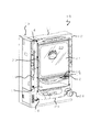
図2に示すように、本実施形態1のパチンコ機10は、大きくは長方形の外枠11と前面枠12とからなり、外枠11の左隣に公知のカードリーダ(プリペイドカードユニット)13が設けられている。前面枠12は、左端上下のヒンジ14により外枠11に対し回動可能に取り付けられている。
前面枠12の下方には上皿15が設けられ、この上皿15に貸出釦16、精算釦17及び残高表示部18が設けられている。カードリーダ13のカード口19にプリペイドカードを挿入すると、記憶された残高が残高表示部18に表示され、貸出釦16を押下すると遊技球の貸出しが実行され上皿15の払い出し口より遊技球が排出される。
A preferred embodiment 1 of the present invention will be described below with reference to the drawings.
As shown in FIG. 2, the pachinko machine 10 according to the first embodiment includes a rectangular outer frame 11 and a front frame 12. A known card reader (prepaid card unit) 13 is located on the left side of the outer frame 11. Is provided. The front frame 12 is rotatably attached to the outer frame 11 by hinges 14 at the upper and lower left ends.
An upper plate 15 is provided below the front frame 12, and a lending button 16, a settlement button 17 and a balance display unit 18 are provided on the upper plate 15. When a prepaid card is inserted into the card slot 19 of the card reader 13, the stored balance is displayed on the balance display unit 18, and when the lending button 16 is pressed, the game ball is lent out and the game ball is loaded from the payout slot of the upper plate 15. Discharged.

前面枠12には、窓状の金枠20が前面枠12に対して解放可能に取り付けられている。この金枠20には板ガラス21が二重にはめ込まれている。板ガラス21の奥には遊技盤22が収納されている。
上皿15の前面枠12下部には、下皿23が設けられ、下皿23の右側には発射ハンドル24が取り付けられている。この発射ハンドル24の外周には、図示しない回動リングが擁され、時計方向に回動すれば遊技球を遊技盤22上に発射することができる。
上皿15と下皿23とは連結されていて、上皿15が遊技球で満杯状態になれば下皿23に遊技球を誘導するよう構成されている。
A window-shaped metal frame 20 is removably attached to the front frame 12 with respect to the front frame 12. A plate glass 21 is double fitted in the metal frame 20. A game board 22 is stored behind the plate glass 21.
A lower plate 23 is provided at the lower part of the front frame 12 of the upper plate 15, and a firing handle 24 is attached to the right side of the lower plate 23. A rotation ring (not shown) is held on the outer periphery of the launch handle 24, and the game ball can be launched onto the game board 22 by rotating clockwise.
The upper plate 15 and the lower plate 23 are connected to each other, and are configured to guide the game ball to the lower plate 23 when the upper plate 15 is full of game balls.

図3はパチンコ機10の裏面図である。図示するように、前述した遊技盤22を脱着可能に取り付ける機構盤26が前述した外枠11に収納されている。この機構盤26には、上方から、球タンク27,誘導樋28及び賞球払出装置29が設けられている。この構成により、遊技盤22上の入賞口に遊技球の入賞があれば球タンク27から誘導樋28を介して所定個数の遊技球を賞球払出装置29により前述した上皿15に排出することができる。
また、機構盤26には遊技制御基板30及び賞球制御基板31が脱着可能に、遊技盤22には特別図柄表示装置32が、前面枠左下部には発射制御基板33が、特別図柄表示装置32の左側に外部接続端子基板50が、各々取り付けられている。
FIG. 3 is a back view of the pachinko machine 10. As shown in the drawing, a mechanism board 26 to which the above-described game board 22 is detachably attached is housed in the above-described outer frame 11. The mechanism panel 26 is provided with a ball tank 27, a guide rod 28, and a prize ball payout device 29 from above. With this configuration, if there is a winning game ball in the winning slot on the game board 22, a predetermined number of gaming balls are discharged from the ball tank 27 via the guide rod 28 to the above-described upper plate 15 by the winning ball dispensing device 29. Can do.
In addition, a game control board 30 and a prize ball control board 31 can be attached to and detached from the mechanism board 26, a special symbol display device 32 is provided on the game board 22, a launch control board 33 is provided on the lower left part of the front frame, and a special symbol display device is provided. External connection terminal boards 50 are respectively attached to the left side of 32.

次に図4を用いて遊技盤22について説明する。
図4に示すように遊技盤22には、中央に特別図柄表示装置32を構成するLCDパネルユニット(以下、「LCD」という。)32a、その下部に第1種始動口としての普通電動役物36、LCD32a上部の普通図柄表示装置37、普通図柄表示装置37に表示される図柄の変動開始に用いられるLCD32aの左右の普通図柄作動ゲート38及び39、普通電動役物36下部の大入賞口40、盤面最下部のアウト口41、その他の各種入賞口、風車及び図示しない遊技釘等が備えられている。
この構成により、前述した発射ハンドル24を回動すれば発射制御基板33により駆動される発射モータ33aが駆動されて上皿15上の遊技球がガイドレールを介して遊技盤22上に発射される。発射された遊技球が各入賞口に入賞すれば遊技球は盤面裏面にセーフ球として取り込まれ、入賞しなければアウト口41を介してアウト球として同様に盤面裏面に取り込まれる。
Next, the game board 22 will be described with reference to FIG.
As shown in FIG. 4, the game board 22 has an LCD panel unit (hereinafter referred to as “LCD”) 32a constituting a special symbol display device 32 at the center, and a normal electric accessory serving as a first type starting port at the lower part thereof. 36, the normal symbol display device 37 on the upper side of the LCD 32a, the normal symbol operation gates 38 and 39 on the left and right of the LCD 32a used for starting the variation of the symbol displayed on the normal symbol display device 37, and the big winning opening 40 on the lower side of the normal electric accessory 36 Further, an out port 41 at the bottom of the board surface, other various winning ports, a windmill, a game nail (not shown) and the like are provided.
With this configuration, when the above-described launch handle 24 is rotated, the launch motor 33a driven by the launch control board 33 is driven, and the game ball on the upper plate 15 is launched onto the game board 22 via the guide rail. . If the launched game ball wins each winning hole, the game ball is taken into the back of the board as a safe ball, and if not won, it is taken into the back of the board through the out port 41 as well.

続いて前述したパチンコ機10の電気的構成を図5のブロック図を用いて説明する。
パチンコ機10の電気回路は、図示するように、前述した遊技制御基板30、賞球制御基板31、特別図柄表示装置32、発射制御基板33、ランプ制御基板34及び音制御基板35等から構成されている。尚、この回路図には、信号の受け渡しを行うために所謂中継基板等は記載していない。
Next, the electrical configuration of the pachinko machine 10 described above will be described with reference to the block diagram of FIG.
As shown in the figure, the electric circuit of the pachinko machine 10 includes the game control board 30, the prize ball control board 31, the special symbol display device 32, the launch control board 33, the lamp control board 34, the sound control board 35, and the like. ing. In this circuit diagram, a so-called relay board or the like is not shown in order to exchange signals.

遊技制御基板30は、遊技制御プログラムを記憶したROM及び演算等の作業領域として働くRAM68,69を内蔵した8ビットワンチップマイコンを中心とした論理演算回路として構成され、この他各基板又は各種スイッチ類及び各種アクチェータ類との入出力を行うための外部入出力回路も設けられている。
遊技制御基板30の入力側には、第1種始動口スイッチ36a、普通図柄作動スイッチ38a及び39a、役物連続作動スイッチ(以下、単に「Vスイッチ」と呼ぶ)40a、カウントスイッチ40b、満タンスイッチ43、補給スイッチ44、複数のその他入賞口スイッチ45、玉抜スイッチ46等が接続されている。また、出力側には、大入賞口ソレノイド40c、Vソレノイド40b、普通役物ソレノイド36b及び外部接続端子基板50等が接続されている。
The game control board 30 is configured as a logic operation circuit centered on an 8-bit one-chip microcomputer incorporating a ROM 68 that stores a game control program and RAMs 68 and 69 that serve as work areas for operations, etc. An external input / output circuit for inputting / outputting data from / to various actuators is also provided.
On the input side of the game control board 30, there are a first type start port switch 36a, normal symbol operation switches 38a and 39a, an accessory continuous operation switch (hereinafter simply referred to as "V switch") 40a, a count switch 40b, a full tank A switch 43, a replenishment switch 44, a plurality of other prize opening switches 45, a ball removal switch 46, and the like are connected. On the output side, a special prize opening solenoid 40c, a V solenoid 40b, a normal accessory solenoid 36b, an external connection terminal board 50, and the like are connected.

第1種始動スイッチ36aは前述した遊技盤22上の普通電動役物36内、普通図柄作動スイッチ38a及び39aは各々普通図柄作動ゲート38及び39内、Vスイッチ40aは大入賞口40内の特定領域内、同じくカウントスイッチ40bは大入賞口40内、満タンスイッチ43は下皿16内、補給スイッチ44は球タンク27内、その他入賞口スイッチ45は普通電動役物36及び大入賞口40以外の盤面上の各々の入賞口、玉抜スイッチ46は賞球払出装置29の近傍に各々取り付けられている。ここで、Vスイッチ40aは大入賞口40内に入賞した遊技球が特別装置作動領域(以下、「特別領域」という。)を通過したことを、カウントスイッチ40bは大入賞口40内に入賞する全ての遊技球を、満タンスイッチ43は下皿16内に遊技球が満タン状態になったことを、補給スイッチ44は球タンク27内に遊技球が存在することを、その他入賞口スイッチ45は普通電動役物36及び大入賞口40以外の盤面上の各々の入賞口に遊技球が入賞したことを、玉抜スイッチ46は玉抜操作ボタンが押下されたことを各々検出するものである。
また、出力側に接続された大入賞口ソレノイド40cは大入賞口40、Vソレノイドは大入賞口40内の特別領域、普通役物ソレノイド36bは普通電動役物36の開閉に各々使用されるものである。
The first type start switch 36a is in the normal electric accessory 36 on the game board 22 described above, the normal symbol operation switches 38a and 39a are in the normal symbol operation gates 38 and 39, respectively, and the V switch 40a is in the special winning opening 40. In the same area, the count switch 40 b is also in the big prize opening 40, the full tank switch 43 is in the lower tray 16, the replenishment switch 44 is in the ball tank 27, and the other prize opening switch 45 is other than the ordinary electric accessory 36 and the big prize opening 40. Each winning opening and ball removal switch 46 on the board surface is attached in the vicinity of the prize ball payout device 29. Here, the V switch 40a wins the prize winning opening 40 when the game ball that has won the prize winning opening 40 has passed the special device operating area (hereinafter referred to as "special area"). For all game balls, the full tank switch 43 indicates that the game ball is full in the lower plate 16, the replenishment switch 44 indicates that there is a game ball in the ball tank 27, and the other prize opening switch 45. Indicates that a game ball has won a prize on each of the prize holes on the board other than the ordinary electric accessory 36 and the big prize opening 40, and the ball removal switch 46 detects that the ball removal operation button has been pressed. .
The large winning opening solenoid 40c connected to the output side is used for the large winning opening 40, the V solenoid is used for a special area in the large winning opening 40, and the ordinary accessory solenoid 36b is used for opening and closing the ordinary electric accessory 36, respectively. It is.

特別図柄表示装置32は、前述したLCD32aと、このLCD32aを駆動制御する図柄表示装置制御基板(以下、単に「図柄制御基板」(「画像制御基板」ともいう。)という。)32b及びバックライト及びインバータ基板等の付属ユニットから構成されている。図柄制御基板32bは、前述した遊技制御基板30と同様8ビットワンチップマイコンを中心とした論理演算回路として構成されている。   The special symbol display device 32 includes the LCD 32a described above, a symbol display device control board (hereinafter simply referred to as “design control board” (hereinafter also referred to as “image control board”)) 32b, a backlight, It consists of accessory units such as an inverter board. Similar to the game control board 30 described above, the symbol control board 32b is configured as a logic operation circuit centered on an 8-bit one-chip microcomputer.

賞球制御基板31は、遊技制御基板30と同様マイクロコンピュータを用いた論理演算回路として構成され、その入力回路には賞球払出スイッチ31a及び貸玉払出スイッチ31bが接続され、出力回路には玉切モータ31c及び玉貸モータ31dが接続されている。また、賞球制御基板31には、前述したカードリーダ13が双方向に接続され、カードリーダ13にはCR精算表示基板47が接続されている。賞球払出スイッチ31aは、遊技制御基板30にも接続されている。
玉切モータ31c及び玉貸モータ31dは、前述した賞球払出装置29に設けられ、誘導樋28から供給される遊技球を下方に所定個数流下させるものである。玉切モータ31cから払い出される遊技球は賞球払出スイッチ31aにより検出され、玉貸モータ31dから払い出される遊技球は貸玉払出スイッチ31bにより検出される。
CR精算表示基板47は、前述した上皿15の貸出釦16、精算釦17及び残高表示部18等から構成されている。尚、CR精算表示基板47を賞球制御基板31に直接に接続する構成としても良い。
The prize ball control board 31 is configured as a logical operation circuit using a microcomputer like the game control board 30, and a prize ball payout switch 31 a and a ball rental payout switch 31 b are connected to the input circuit, and a ball is supplied to the output circuit. A cutting motor 31c and a ball lending motor 31d are connected. Further, the card reader 13 described above is bidirectionally connected to the prize ball control board 31, and a CR settlement display board 47 is connected to the card reader 13. The prize ball payout switch 31 a is also connected to the game control board 30.
The ball cutting motor 31c and the ball lending motor 31d are provided in the prize ball payout device 29 described above, and flow down a predetermined number of game balls supplied from the guide rod 28. A game ball paid out from the ball cutting motor 31c is detected by the prize ball payout switch 31a, and a game ball paid out from the ball rental motor 31d is detected by the ball rental payout switch 31b.
The CR adjustment display board 47 includes the lending button 16, the adjustment button 17, and the balance display unit 18 of the upper plate 15 described above. The CR adjustment display board 47 may be connected directly to the prize ball control board 31.

前記構成により遊技制御基板30から賞球払い出し指令のデータが送信されると、このデータを受信した賞球制御基板31は、未払の賞球データに送信されたデータが示す賞球個数を加算して新たな賞球データとして記憶し、所定個数の遊技球を賞球として払い出した後に賞球払出スイッチ31aにより検出された遊技球を記憶した賞球データから減算処理を実行して新たな賞球データとし、この賞球データの値が零になるまで払い出し処理を実行する。
一方、CR精算表示基板47の貸出釦16を押下すると、100円の場合はカードリーダ13から賞球制御基板31に1パルスの信号が送信され、500円の場合には5パルスの信号が送信される。賞球制御基板31は、1パルスの信号に対して25個の遊技球が貸玉払出スイッチ31bにより検出されるまで玉貸モータ31dを駆動制御して貸し玉を払い出す処理を実行する。
When prize ball payout command data is transmitted from the game control board 30 with the above configuration, the prize ball control board 31 that has received this data adds the number of prize balls indicated by the transmitted data to the unpaid prize ball data. Then, it is stored as new prize ball data, and after subtracting a predetermined number of game balls as prize balls, a subtraction process is executed from the prize ball data stored with the game balls detected by the prize ball payout switch 31a to obtain a new prize. The payout process is executed until the value of the prize ball data becomes zero.
On the other hand, when the lending button 16 on the CR adjustment display board 47 is pressed, a 1-pulse signal is transmitted from the card reader 13 to the prize ball control board 31 in the case of 100 yen, and a 5-pulse signal is transmitted in the case of 500 yen. Is done. The prize ball control board 31 executes a process of paying out the lending balls by drivingly controlling the ball lending motor 31d until 25 game balls are detected by the ball lending payout switch 31b for one pulse signal.

発射制御基板33は、遊技者が操作する発射ハンドル24の回動量に応じて発射モータ33aを駆動制御するものであり、その他遊技者が発射停止スイッチ24bを押下したとき発射を停止させたり、発射ハンドル24に内蔵された前記タッチスッチ24aがオン状態のときタッチランプ48を点灯させるものである。
タッチスイッチ24aは発射ハンドル24に内蔵され遊技者が発射ハンドル24に触れていることを検出する。
The launch control board 33 drives and controls the launch motor 33a according to the amount of rotation of the launch handle 24 operated by the player. When the player presses the launch stop switch 24b, the launch control board 33 stops firing or launches. When the touch switch 24a built in the handle 24 is in an ON state, the touch lamp 48 is turned on.
The touch switch 24 a is built in the firing handle 24 and detects that the player is touching the firing handle 24.

ランプ制御基板34は主としてトランジスタ等の駆動素子から構成されており、遊技制御基板30からの指令を受けて普通図柄表示装置37、大当たりランプやエラーランプ等のランプ類及びLED等の各種ランプ類を点灯表示させるものである。   The lamp control board 34 is mainly composed of drive elements such as transistors. Upon receiving a command from the game control board 30, the normal symbol display device 37, lamps such as jackpot lamps and error lamps, and various lamps such as LEDs are provided. Lights up and displays.

音制御基板35は音源IC及びアンプ等から構成されており、遊技制御基板30の指令を受けてスピーカ49を駆動制御するものである。   The sound control board 35 includes a sound source IC, an amplifier, and the like, and controls driving of the speaker 49 in response to a command from the game control board 30.

前述した特別図柄表示装置32、賞球制御基板31、発射制御基板33、ランプ制御基板34及び音制御基板35への送信は、遊技制御基板30からのみ送信することができるよう一方向通信の回路として構成されている。この一方向通信の回路は、インバータ回路又はラッチ回路を用いて具現化することができる。一方向通信の回路に代えて、双方向通信の回路としてもよい。   A circuit for one-way communication so that transmission to the special symbol display device 32, prize ball control board 31, launch control board 33, lamp control board 34, and sound control board 35 described above can be transmitted only from the game control board 30. It is configured as. This one-way communication circuit can be realized using an inverter circuit or a latch circuit. A bidirectional communication circuit may be used instead of the one-way communication circuit.

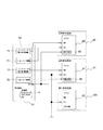
前記遊技制御基板30、賞球制御基板31、図柄制御基板32b、発射制御基板33、ランプ制御基板34及び音制御基板35等へは、図6に示すように、電源基板51から各種電源が供給されている。
電源基板51は、24V交流電源からDC32V、DC12V、DC5V、更にコンデンサによりDC5Vのバックアップ電源を生成し、各制御基に必要な電源を供給するよう構成されている。
DC5Vのバックアップ電源は、遊技制御基板30と賞球制御基板31に供給されている。
As shown in FIG. 6, various power supplies are supplied from the power supply board 51 to the game control board 30, the prize ball control board 31, the symbol control board 32b, the launch control board 33, the lamp control board 34, the sound control board 35, and the like. Has been.
The power supply board 51 is configured to generate a backup power of DC5V from a 24V AC power supply using DC32V, DC12V, DC5V, and a capacitor, and supply necessary power to each control base.
The backup power of DC5V is supplied to the game control board 30 and the prize ball control board 31.

図7に示す通り、電源基板51と、遊技制御基板30、賞球払出制御基板31を含む遊技機各部との間の給電および信号系を示す。各パチンコ遊技機10の電源基板51は、パチンコ店側に設けられたAC24V電源を電源スイッチ52を介して電源生成回路53が受けており、電源生成回路53が、図示の遊技制御基板30、賞球払出制御基板31を含む遊技機各部に給電する。電源スイッチ52はオンまたはオフの操作をするとその状態を保持するタイプが用いられる。   As shown in FIG. 7, the power supply and signal system between the power supply board 51 and each part of the gaming machine including the game control board 30 and the prize ball payout control board 31 are shown. The power supply board 51 of each pachinko gaming machine 10 receives the AC 24V power provided on the pachinko parlor side via the power switch 52 by the power supply generation circuit 53, and the power supply generation circuit 53 is connected to the game control board 30 shown in the figure. Power is supplied to each part of the gaming machine including the ball payout control board 31. The power switch 52 is of a type that maintains its state when turned on or off.

電源生成回路53における全波24V出力は電源電圧監視回路54に入力し、電源電圧監視回路54による全波24V出力の有無の検出結果に基づいてリセット信号発生回路55がリセット信号を出力もしくは解除する。すなわち、電源電圧監視回路54は所定の基準電圧以上の非出力状態が所定の時間、維持すれば全波24V出力停止と判断し、リセット信号発生回路55は全波24V出力停止との判断に応じてリセット信号を出力する。一方、全波24V出力が開始されるとリセット信号は解除される。ここで、リセット信号の出力とはロウレベルの信号を出力することであり、解除とはロウレベルからハイレベルに変化することをいう。なお、リセット信号の解除は、全波24V出力の検出時点から遅延時間Taの後になされる(図13参照)。   The full-wave 24V output in the power generation circuit 53 is input to the power supply voltage monitoring circuit 54, and the reset signal generation circuit 55 outputs or cancels the reset signal based on the detection result of the presence or absence of the full-wave 24V output by the power supply voltage monitoring circuit 54. . That is, the power supply voltage monitoring circuit 54 determines that the full-wave 24V output is stopped if the non-output state higher than the predetermined reference voltage is maintained for a predetermined time, and the reset signal generation circuit 55 responds to the determination that the full-wave 24V output is stopped. Output a reset signal. On the other hand, when full wave 24V output is started, the reset signal is canceled. Here, the output of the reset signal is to output a low level signal, and the release is to change from the low level to the high level. The reset signal is released after the delay time Ta from the time point when the full-wave 24V output is detected (see FIG. 13).

リセット信号発生回路55の出力は遊技制御基板30、賞球払出制御基板31それぞれの遅延回路56,57を介して各制御基板30、31のCPU60、61のリセット端子に出力される。遊技制御基板30の遅延回路56ではリセット信号の解除に所定の遅延時間Tcが与えられ、賞球払出制御基板31の遅延回路57ではリセット信号の解除に所定の遅延時間Tbが与えられる(図13参照)。図8に示す通り、図柄制御基板32bのCPUについても同様である。   The output of the reset signal generation circuit 55 is output to the reset terminals of the CPUs 60 and 61 of the control boards 30 and 31 via the delay circuits 56 and 57 of the game control board 30 and the prize ball payout control board 31, respectively. The delay circuit 56 of the game control board 30 is given a predetermined delay time Tc for releasing the reset signal, and the delay circuit 57 of the prize ball payout control board 31 is given a predetermined delay time Tb for releasing the reset signal (FIG. 13). reference). The same applies to the CPU of the symbol control board 32b as shown in FIG.

電源電圧監視回路54の出力と接続する入力を備える停電信号発生回路64が設けてあり、停電等の電源遮断時に停電信号を各制御基板CPU60、61のNMI端子に出力するようになっている。停電信号は電源遮断に伴ってハイレベルからロウレベルに変化する信号であり、リセット信号が出力するに先立って出力するように出力タイミングが設定されている。   A power failure signal generation circuit 64 having an input connected to the output of the power supply voltage monitoring circuit 54 is provided, and a power failure signal is output to the NMI terminals of the control board CPUs 60 and 61 when the power supply is interrupted such as a power failure. The power failure signal is a signal that changes from a high level to a low level when the power is cut off, and the output timing is set so that it is output before the reset signal is output.

また、電源基板51は、コンデンサを含み構成されたバックアップ電源生成回路65によりDC5Vのバックアップ電源(VBB)を生成する構成となっており、バックアップ電源(VBB)出力は各制御基板CPU60、61のバックアップ端子(VBB)に出力され、停電時には後述するように各制御基板30、31のバッテリバックアップRAM68,69の記憶内容をそれぞれ保持する。   The power supply board 51 is configured to generate a DC5V backup power supply (VBB) by a backup power supply generation circuit 65 including a capacitor, and the backup power supply (VBB) output is a backup of each control board CPU60, 61. It is output to the terminal (VBB), and holds the stored contents of the battery backup RAMs 68 and 69 of the control boards 30 and 31, respectively, at the time of a power failure, as will be described later.

遊技制御基板30は、RAMクリアスイッチ66を備えている。RAMクリアスイッチ66は制御基板CPU60、61のバッテリバックアップRAM68,69に記憶されている内容をクリアするために設けられる。RAMクリアスイッチ66の出力信号はRAMクリア信号発生回路67に入力される。またリセット信号発生回路55のリセット出力は、RAMクリア信号発生回路67に入力される。   The game control board 30 includes a RAM clear switch 66. The RAM clear switch 66 is provided to clear the contents stored in the battery backup RAMs 68 and 69 of the control board CPUs 60 and 61. The output signal of the RAM clear switch 66 is input to the RAM clear signal generation circuit 67. The reset output of the reset signal generation circuit 55 is input to the RAM clear signal generation circuit 67.

RAMクリアスイッチ66には押下時のみオンする押し釦タイプのものが用いられ、上記リセット信号の立ち上がり時にRAMクリアスイッチ66がオンであれば、遊技制御基板30に設けたRAMクリア信号発生回路67が、ハイレベルの信号であるRAMクリア信号を遊技制御基板30、賞球制御基板31それぞれの入力ポート71、72に一定時間Tgの間、出力する(図13参照)。すなわち、RAMクリア信号はリセット信号が解除される電源投入時のみ出力される。ここで電源スイッチ52のオンからリセット信号立ち上がりまでの遅延時間Taは例えば100msに設定され、RAMクリア信号を発生させるにはRAMクリアスイッチ66を押下しながら電源スイッチ52をオンすることになる。なお、各制御基板CPU60、61は入力ポート71、72におけるRAMクリア信号の有無をデータバスを介して監視する。   The RAM clear switch 66 is a push button type that is turned on only when pressed, and if the RAM clear switch 66 is turned on at the rising edge of the reset signal, a RAM clear signal generating circuit 67 provided on the game control board 30 is used. The RAM clear signal, which is a high level signal, is output to the input ports 71 and 72 of the game control board 30 and the prize ball control board 31 for a predetermined time Tg (see FIG. 13). That is, the RAM clear signal is output only when the power is turned on when the reset signal is released. Here, the delay time Ta from the turn-on of the power switch 52 to the rise of the reset signal is set to 100 ms, for example. To generate the RAM clear signal, the power switch 52 is turned on while the RAM clear switch 66 is depressed. Each control board CPU 60, 61 monitors the presence or absence of a RAM clear signal at the input ports 71, 72 via the data bus.

次に、図8に示すように、電源基板51の電源電圧監視回路54には、リセット1回路74及びリセット2回路75、バックアップ1電圧監視回路76およびバックアップ2電圧監視回路77が備えられている。
リセット1回路74は、遊技制御基板30のCPU60のリセット端子RESに接続されている。
リセット2回路75は、賞球制御基板31のCPU61のリセット端子RES、図柄制御基板32bのCPU62のリセット端子RES等に接続されている。
バックアップ1電圧監視回路76は、遊技制御基板30のCPU60の強制割り込み端子NMIに接続されている。
バックアップ2電圧監視回路77は、賞球制御基板31のCPU61の強制割り込み端子NMIに接続されている。
尚、前述したように、5Vバックアップ電源は、遊技制御基板30のCPU60のバックアップ端子VBB、及び賞球制御基板31のCPU61のバックアップ端子VBBに接続されている。
Next, as shown in FIG. 8, the power supply voltage monitoring circuit 54 of the power supply substrate 51 includes a reset 1 circuit 74 and a reset 2 circuit 75, a backup 1 voltage monitoring circuit 76, and a backup 2 voltage monitoring circuit 77. .
The reset 1 circuit 74 is connected to the reset terminal RES of the CPU 60 of the game control board 30.
The reset 2 circuit 75 is connected to the reset terminal RES of the CPU 61 of the winning ball control board 31, the reset terminal RES of the CPU 62 of the symbol control board 32b, and the like.
The backup 1 voltage monitoring circuit 76 is connected to the forced interrupt terminal NMI of the CPU 60 of the game control board 30.
The backup 2 voltage monitoring circuit 77 is connected to the forced interrupt terminal NMI of the CPU 61 of the prize ball control board 31.
As described above, the 5V backup power source is connected to the backup terminal VBB of the CPU 60 of the game control board 30 and the backup terminal VBB of the CPU 61 of the prize ball control board 31.

リセット1回路74は、図9に示すように、電圧監視IC11、抵抗器R17、R18及びR19、バイバスコンデンサC10等から構成されている。電圧監視IC11の入力端子であるVSB端子には、抵抗器R17とR18とで分圧したDC12Vの電源が供給され、出力端子であるRESET端子は、抵抗器R19でDC5Vにプルアップされている。
前記構成により電圧監視IC11の出力端子であるRESET端子は、DC12V電源の電圧が9.39〜10.21V以下に低下すると、出力するリセット信号1を、ハイレベルからロウレベルに変化させる。
As shown in FIG. 9, the reset 1 circuit 74 includes a voltage monitoring IC 11, resistors R17, R18 and R19, a bypass capacitor C10, and the like. The VSB terminal that is the input terminal of the voltage monitoring IC 11 is supplied with a DC12V power source divided by the resistors R17 and R18, and the RESET terminal that is the output terminal is pulled up to DC5V by the resistor R19.
With the above configuration, the RESET terminal, which is the output terminal of the voltage monitoring IC 11, changes the reset signal 1 to be output from the high level to the low level when the voltage of the DC12V power supply decreases to 9.39 to 10.21V or less.

リセット2回路75は、図10に示すように、電圧監視IC8、抵抗器R38、R39及び40、バイパスコンデンサC22及びC23等から構成されている。電圧監視IC8の入力端子であるVS端子には、抵抗器R39とR40とで分圧したDC12Vの電源が供給され、出力端子であるRESET端子は、抵抗器R38でDC5Vにプルアップされている。
前記構成により電圧監視IC8の出力端子であるRESET端子は、DC12V電源の電圧が7.20〜7.75V以下に低下すると、出力するリセット信号2を、ハイレベルからロウレベルに変化させる。
As shown in FIG. 10, the reset 2 circuit 75 includes a voltage monitoring IC 8, resistors R38, R39 and 40, bypass capacitors C22 and C23, and the like. The VS terminal that is the input terminal of the voltage monitoring IC 8 is supplied with a DC12V power source divided by the resistors R39 and R40, and the RESET terminal that is the output terminal is pulled up to DC5V by the resistor R38.
With the above configuration, the RESET terminal that is the output terminal of the voltage monitoring IC 8 changes the reset signal 2 to be output from the high level to the low level when the voltage of the DC12V power supply drops to 7.20 to 7.75 V or less.

バックアップ1電圧監視回路76は、図11に示すように、コンパレータIC1A、抵抗器R41〜45等から構成されている。コンパレータIC1Aのマイナス入力端子には、抵抗器R43とR44とで分圧したDC5Vの電源が供給され、プラス入力端子には、抵抗器R41とR42とで分圧したDC12Vの電源が供給され、出力端子は抵抗器R45でDC5Vにプルアップされている。
前記構成によりコンパレータIC1Aの出力端子は、DC12V電源の電圧が10.25〜10.70V以下に低下すると、出力するバックアップ信号1を、ハイレベルからロウレベルに変化させる。
As shown in FIG. 11, the backup 1 voltage monitoring circuit 76 includes a comparator IC 1A, resistors R41 to R41, and the like. The negative input terminal of the comparator IC1A is supplied with a DC5V power source divided by resistors R43 and R44, and the positive input terminal is supplied with a DC12V power source divided by resistors R41 and R42 for output. The terminal is pulled up to DC5V by resistor R45.
With the configuration described above, the output terminal of the comparator IC1A changes the backup signal 1 to be output from the high level to the low level when the voltage of the DC12V power supply decreases to 10.25 to 10.70V or less.

バックアップ2電圧監視回路77は、図12に示すように、コンパレータIC2A、抵抗器R51〜R55等から構成されている。コンパレータIC2Aのマイナス入力端子には、抵抗器R53とR54とで分圧したDC5Vの電源が供給され、プラス入力端子には、抵抗器R51とR52とで分圧したDC12Vの電源が供給され、出力端子は抵抗器R55でDC5Vにプルアップされている。
前記構成によりコンパレータIC2Aの出力端子は、DC12V電源の電圧が8.00〜9.23V以下に低下すると、出力するバックアップ信号2を、ハイレベルからロウレベルに変化させる。
As shown in FIG. 12, the backup 2 voltage monitoring circuit 77 includes a comparator IC 2A, resistors R51 to R55, and the like. The negative input terminal of the comparator IC2A is supplied with a DC5V power source divided by resistors R53 and R54, and the positive input terminal is supplied with a DC12V power source divided by resistors R51 and R52 for output. The terminal is pulled up to DC5V by a resistor R55.
With the configuration described above, the output terminal of the comparator IC2A changes the backup signal 2 to be output from the high level to the low level when the voltage of the DC12V power supply decreases to 8.00 to 9.23V or less.

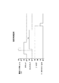
本パチンコ遊技機10の電源投入時の処理の流れについて図13を参照して説明する。RAMクリアスイッチ66を押下しながら電源スイッチ52をオンし電源基板51から給電を開始した時の電源基板51、遊技制御基板30および賞球制御基板31各部の作動状態を示す。   A flow of processing when the pachinko gaming machine 10 is turned on will be described with reference to FIG. The operation state of each part of the power supply board 51, the game control board 30, and the prize ball control board 31 when the power supply switch 52 is turned on while the RAM clear switch 66 is pressed and power supply is started from the power supply board 51 is shown.

電源スイッチ52のオンから時間Ta経過後にリセット信号が解除され、このリセット信号解除が遊技制御基板CPU60においては時間Tc経過後に、賞球制御基板CPU61においては時間Tb経過後に有効になると、有効になった時点から各制御基板CPU60、61がセキュリティチェックを開始する。ここで、遊技制御基板CPU60の遅延時間Tcが賞球制御基板CPU61の遅延時間Tbよりも長く設定されている。セキュリティチェック時間Td,TeはCPUの種類、システムクロック周波数等にもよるが、本具体例において遊技制御基板CPU60、賞球制御基板CPU61両方に使用したLE2080A-PA(システムクロック周波数6MHz)では、それぞれ、439ms、200msとした。Td,Teは同一値(例えば、185ms)でもよい。なお、セキュリティチェックとは、周知のごとくワンチップマイコンである各CPU60、61等が遊技の進行内容を書き込んだROMの内容が正規の内容であるか否かをチェックすることである。   The reset signal is released after the time Ta has elapsed since the power switch 52 was turned on. This reset signal release becomes effective when the time Tc elapses in the game control board CPU60 and after the time Tb elapses in the prize ball control board CPU61. Each control board CPU 60, 61 starts a security check from that time. Here, the delay time Tc of the game control board CPU60 is set longer than the delay time Tb of the prize ball control board CPU61. The security check times Td and Te depend on the CPU type, system clock frequency, etc., but in the LE2080A-PA (system clock frequency 6 MHz) used for both the game control board CPU 60 and the prize ball control board CPU 61 in this specific example, respectively. 439 ms and 200 ms. Td and Te may be the same value (for example, 185 ms). As is well known, the security check is to check whether or not the contents of the ROM in which the CPU 60, 61, etc., which are one-chip microcomputers, write the game progress contents are regular contents.

遊技制御基板CPU60のセキュリティチェック時間Tdが賞球制御基板CPU61のセキュリティチェック時間Teと同等以上で、かつ、遊技制御基板CPU60のセキュリティチェック開始時期が賞球制御基板CPU61のセキュリティチェック開始時期よりも遅く実行されるようになっていれば(Tb<Tc)、遊技制御基板CPU60のセキュリティチェック完了時には賞球制御基板CPU61はセキュリティチェックが完了し、遊技制御基板CPU60がROMに書き込まれたプログラムにしたがって遊技の制御を開始する時には、賞球制御基板CPU61は既に遊技の制御を実行している。この結果、電源投入後、遊技制御基板CPU60が直ちに賞球制御基板CPU61にデータを送信しても、賞球制御基板CPU61はセキュリティチェックを終え自身の制御を実行しているので確実にデータを受信することができる。なお、遊技制御基板CPU60のセキュリティチェック時間Tdが賞球制御基板CPU61のセキュリティチェック時間Teと同一或いは短くてしてもよい。   The security check time Td of the game control board CPU60 is equal to or longer than the security check time Te of the prize ball control board CPU61, and the security check start time of the game control board CPU60 is later than the security check start time of the prize ball control board CPU61. If it is to be executed (Tb <Tc), when the security check of the game control board CPU 60 is completed, the prize ball control board CPU 61 completes the security check, and the game control board CPU 60 follows the program written in the ROM. When starting this control, the prize ball control board CPU 61 has already executed the game control. As a result, even if the game control board CPU60 immediately sends data to the prize ball control board CPU61 after the power is turned on, the prize ball control board CPU61 has finished the security check and has executed its own control, so it has received the data reliably. can do. The security check time Td of the game control board CPU 60 may be the same as or shorter than the security check time Te of the prize ball control board CPU 61.

一方、RAMクリアスイッチ66を押しながら電源スイッチ52をオンしているので、遊技制御基板30からは、リセット信号が立ち上がった時点からRAMクリア信号が時間Tgの間、各基板60,61の入力ポート71,72に出力されることになる。ここで、RAMクリア信号の出力時間Tgを、セキュリティチェックの遅く完了する遊技制御基板CPU60についてのリセット信号解除からセキュリティチェック完了までの時間(リセット信号遅延時間Tc+セキュリティチェック時間Td)を考慮して、賞球制御基板CPU61がセキュリティチェック完了後にRAMクリア信号を確実に受信できるようにする。   On the other hand, since the power switch 52 is turned on while the RAM clear switch 66 is being pressed, the game control board 30 receives the RAM clear signal for the time Tg from the time when the reset signal rises. 71 and 72 are output. Here, the RAM clear signal output time Tg is taken into consideration the time from the reset signal release to the security check completion (reset signal delay time Tc + security check time Td) for the game control board CPU 60 that is completed late in the security check. The award ball control board CPU 61 can reliably receive the RAM clear signal after the security check is completed.

パチンコ機10に電源が投入されたときの遊技制御基板30と、遊技制御基板30以外のサブ制御基板である、賞球制御基板31及び図柄制御基板32b等との各々のCPUの動作又は制御動作の立ち上がり状態を、図14に示すタイミングチャートに従って説明する。
パチンコ機10に電源が投入されると、電源基板51によりDC32V、DC12V、バッテリバックアップ電源(VBB)であるDC5Vが生成される。この生成された各電源は各制御基板に供給されるが、リセット1回路74及びリセット2回路75の働きにより賞球制御基板31等の各サブ制御基板及び遊技制御基板30は次のように動作の立ち上げ処理を行う。
CPU operation or control operation of the game control board 30 when the power is turned on to the pachinko machine 10 and the sub-control board other than the game control board 30 such as the prize ball control board 31 and the symbol control board 32b Will be described with reference to the timing chart shown in FIG.
When the pachinko machine 10 is powered on, the power board 51 generates DC 32V, DC 12V, and DC 5V, which is a battery backup power source (VBB). Each generated power supply is supplied to each control board, but the sub-control board such as the prize ball control board 31 and the game control board 30 operate as follows by the action of the reset 1 circuit 74 and the reset 2 circuit 75. Start up processing.

図14に示すように、電源基板51に電源が投入されると(ポイントP1)、DC12V電源の電圧は放物線を描いて漸次0Vから12Vに立ち上がる。この漸次立ち上がるDC12V電源の電圧が、基準値LV2(本具体例では、7.20〜7.75V)になるとリセット2回路60の出力信号であるリセット信号2がロウレベルからハイレベルとなる。これにより、サブ制御基板の各CPUのリセットが解除され、賞球制御基板31のCPU61がセキュリティチェック動作を開始する(ポイントP2)。このとき、本具体例では、賞球制御基板31を除く図柄制御基板32b等の各サブ制御基板は、セキュリティチェック動作は実行せずに本来の制御を実行するよう構成されている。
DC12Vの電源電圧が基準値LV2のときには、リセット1回路74の出力信号であるリセット信号1は、まだロウレベルの状態を維持している。従って、遊技制御基板30のCPU60は、まだ立ち上がっていない。
As shown in FIG. 14, when the power supply is turned on to the power supply board 51 (point P1), the voltage of the DC12V power supply gradually rises from 0V to 12V in a parabolic manner. When the voltage of the DC12V power supply that gradually rises to the reference value LV2 (in this specific example, 7.20 to 7.75V), the reset signal 2 that is the output signal of the reset 2 circuit 60 changes from the low level to the high level. Thereby, the reset of each CPU of the sub control board is released, and the CPU 61 of the prize ball control board 31 starts a security check operation (point P2). At this time, in this specific example, each sub-control board such as the symbol control board 32b excluding the prize ball control board 31 is configured to execute the original control without executing the security check operation.
When the power supply voltage of DC12V is the reference value LV2, the reset signal 1 that is the output signal of the reset 1 circuit 74 is still in the low level state. Therefore, the CPU 60 of the game control board 30 has not been started up yet.

DC12Vの電源電圧が基準値LV2から基準値LV1(本具体例では、9.39〜10.21V)に上昇すると、リセット1回路74のリセット信号1は、ロウレベルからハイレベルとなる。これにより、遊技制御基板30のCPU60のリセットが解除され、CPU60がセキュリティチェック動作を開始する(ポイントP3)。
遊技制御基板30のCPU60のセキュリティチェック設定時間Tdは、賞球制御基板31のCPU61のセキュリティチェック設定時間Teと同等かそれ以上長くなるように設計されている。
尚、セキュリティチェックとは、周知の如く、ワンチップマイコンであるCPU63及び64が遊技の進行内容を書き込んだROMの内容が正規の内容であるか否かをチェックする機能のことである。
When the power supply voltage of DC12V rises from the reference value LV2 to the reference value LV1 (in this specific example, 9.39 to 10.21V), the reset signal 1 of the reset 1 circuit 74 changes from the low level to the high level. Thereby, reset of CPU60 of game control board 30 is canceled, and CPU60 starts security check operation (point P3).
The security check setting time Td of the CPU 60 of the game control board 30 is designed to be equal to or longer than the security check setting time Te of the CPU 61 of the prize ball control board 31.
As is well known, the security check is a function in which the CPUs 63 and 64, which are one-chip microcomputers, check whether or not the content of the ROM into which the game progress is written is normal.

遊技制御基板30のセキュリティチェック設定時間Tdが賞球制御基板31のセキュリティチェック設定時間Te以上であり、且つ遊技制御基板30のCPU60のリセット解除時点が各サブ制御基板のCPUのリセット解除時点より遅い。これにより、遊技制御基板30のCPU60がROMに書き込まれたプログラムに従って遊技の制御を実行開始するときには、各サブ制御基板は既に遊技の制御を実行している。この結果、電源投入後直ちに、遊技制御基板30のCPU60が各サブ制御基板にデータを送信しても、各サブ制御基板は本来の制御を実行しているので確実にデータを受信することができる。
尚、本具体例では、セキュリティチェック設定時間Tdは約439msであり、遊技制御基板30のCPU60が電源の投入から遊技の制御を実行するまでの時間は、約529ms〜549msである。また、セキュリティチェック設定時間Teは約200msであり、サブ制御基板の1つである賞球制御基板31のCPU61が電源の投入から遊技の制御を実行するまでの時間は、約202ms〜203msである。
The security check setting time Td of the game control board 30 is equal to or longer than the security check setting time Te of the prize ball control board 31, and the reset release time of the CPU 60 of the game control board 30 is later than the reset release time of the CPU of each sub control board 30. . Thereby, when the CPU 60 of the game control board 30 starts to execute the game control according to the program written in the ROM, each sub-control board has already executed the game control. As a result, even if the CPU 60 of the game control board 30 transmits data to each sub-control board immediately after the power is turned on, each sub-control board is executing the original control, so that the data can be reliably received. .
In this specific example, the security check setting time Td is about 439 ms, and the time from when the CPU 60 of the game control board 30 turns on the power to the control of the game is about 529 ms to 549 ms. The security check set time Te is about 200 ms, and the time from when the CPU 61 of the prize ball control board 31 which is one of the sub-control boards is turned on to control the game is about 202 ms to 203 ms. .

なお、パチンコ遊技機10への電源投入が遮断されるときの動作については、説明は省略する。これについては特許第3444485号の段落第0041〜0044及び図12、図13を参照されたい。バックアップRAM68,69に記憶されるデータは電源遮断時の賞球払い出し状態及び/又は玉貸しの貸し出し状態を示すデータである(以下、単にデータという)。なお、ステップを単にSと略記する。   In addition, description is abbreviate | omitted about operation | movement when the power supply to the pachinko machine 10 is interrupted | blocked. Refer to paragraphs 0041 to 0044 of FIGS. 3444485 and FIGS. 12 and 13 for this. The data stored in the backup RAMs 68 and 69 is data indicating a prize ball payout state and / or a ball lending state when the power is shut off (hereinafter simply referred to as data). The step is simply abbreviated as S.

図15に主制御基板CPU60の電源投入時処理のフローチャートを示す。セキュリティチェックが完了しバッテリバックアップRAM68へのアクセスが許可されると(S101)、RAMクリア信号がオンか否か(S102)、バックアップフラグ(非停電復旧時又は停電復旧時かのいずれかを「0」「1」で示す)がオンか否か(S103)に基づいてパチンコ遊技機10を初期状態から起動する(S104〜S109)か、パチンコ遊技機10を電源遮断前の状態から起動する(S110〜S111)かを判断する。   FIG. 15 shows a flowchart of the power-on process of the main control board CPU60. When the security check is completed and access to the battery backup RAM 68 is permitted (S101), whether or not the RAM clear signal is ON (S102) and the backup flag (when the power failure is restored or when the power failure is restored are set to “0”. "Indicated by" 1 ") is turned on (S103), the pachinko gaming machine 10 is started from the initial state (S104 to S109), or the pachinko gaming machine 10 is started from the state before power-off (S110). To S111).

S102が肯定判断された場合、S103が否定判断された場合には、スタックの設定処理(S104)、RAM68の作業領域のクリア処理(S105)を実行し、作業領域を初期化する(S106)。次いで、特別図柄表示装置32へ、初期画面を表示する旨のコマンドデータを送信し(S107)、ランプ制御基板34へ、初期装飾を表示すべき旨のコマンドデータを送信する(S108)。以降、通常時の処理となる(S109)。   If S102 is affirmed or if S103 is negative, stack setting processing (S104) and work area clear processing (S105) of the RAM 68 are executed to initialize the work area (S106). Next, command data for displaying the initial screen is transmitted to the special symbol display device 32 (S107), and command data for displaying the initial decoration is transmitted to the lamp control board 34 (S108). Thereafter, the normal processing is performed (S109).

S103が否定判断された場合には、電源遮断前の記憶内容をRAM68が保持しているということであり、電源復帰時処理が実行され(S110)、バックアップされたパチンコ遊技機10の状態を示す情報に基づいて停電発生により中断された遊技進行プログラムが再開される(S111)。電源復帰時処理では各サブ制御基板31〜35に停電から復旧したことを報知するコマンドコードを送信する。このコマンドコードを受信した特別図柄表示装置32はLCD32aの画面上に「停電復旧処理中」、「停電前のゲーム内容から続行しています」等のメッセージを表示する処理を行う。あるいは音制御基板35が音声により上記メッセージと同等の内容で停電があったことを報知する。   If the determination in S103 is negative, it means that the RAM 68 holds the memory content before the power is shut off, and the power recovery process is executed (S110), indicating the state of the pachinko gaming machine 10 that has been backed up. Based on the information, the game progress program suspended due to the occurrence of a power failure is resumed (S111). In the power recovery process, a command code notifying that the sub-control boards 31 to 35 have recovered from the power failure is transmitted. Upon receiving this command code, the special symbol display device 32 performs a process of displaying a message such as “Now recovering from power failure” or “Continue from game content before power failure” on the screen of the LCD 32a. Alternatively, the sound control board 35 notifies the user that a power failure has occurred with the same content as the message.

このルーチンにより、停電復旧時か否か判断されるが、本具体例では、DC5Vのバックアップ電源は、前述したように、コンデンサにより約1時間20分〜約3時間30分間CPU60及びCPU61のRAM68,69に記憶されたデータを記憶保持するよう構成されている。このため、停電ではなく、営業が終了してから翌朝に電源を投入する通常状態では、RAM68,69のデータは記憶保持されていない。これにより、停電時にRAM68,69の所定領域に書き込まれた所定値は、記憶保持されることなく所定値とは異なった値となっている。一方、瞬停を含む一般的な停電は、1時間もあれば復旧する。斯かる停電時には、RAM68,69の所定領域に書き込まれた所定値は、変化することなく記憶保持されている。従って、RAM68,69の所定領域に書き込まれた値を比較することにより、停電復旧時か否かが判定される。   In this specific example, it is determined by this routine whether or not the power failure is restored. As described above, the backup power source of DC5V is supplied from the CPUs 60 and 61 by the capacitors 60 to 61 for about 1 hour 20 minutes to about 3 hours 30 minutes. The data stored in 69 is stored and held. For this reason, the data in the RAMs 68 and 69 are not stored and held in a normal state in which the power is turned on the next morning after the end of business rather than a power failure. Thereby, the predetermined value written in the predetermined area of the RAMs 68 and 69 at the time of a power failure is a value different from the predetermined value without being stored and held. On the other hand, a general power failure including a momentary power outage is restored after one hour. At the time of such a power failure, the predetermined value written in the predetermined area of the RAMs 68 and 69 is stored and held without change. Therefore, by comparing the values written in the predetermined areas of the RAMs 68 and 69, it is determined whether or not the power is restored.

また、RAMクリア信号がオンの時にパチンコ遊技機10を初期状態に戻すことができるが、RAMクリア信号は上記のごとくRAMクリアスイッチ66を押下しながら電源スイッチ52をオンした時にのみ生成されるから、RAMクリアスイッチ66を電源スイッチ52をオンする時以外で押下してもRAMクリアがなされることがなく不用意にパチンコ遊技機10が初期状態に戻されることを防止できる。   Further, the pachinko gaming machine 10 can be returned to the initial state when the RAM clear signal is on, but the RAM clear signal is generated only when the power switch 52 is turned on while pressing the RAM clear switch 66 as described above. Even if the RAM clear switch 66 is pressed other than when the power switch 52 is turned on, the RAM is not cleared and the pachinko gaming machine 10 can be prevented from being returned to the initial state carelessly.

本パチンコ遊技機10は、電源スイッチ52と、電源スイッチ52のオンに応じてリセット信号は出力するリセット信号発生回路55と、RAMクリアスイッチ66と、RAMクリア信号発生回路67と、を具備している。ここで電源スイッチ52の投入に伴うリセット信号はロウレベルからハイレベルへの変化であり、この変化は、電源スイッチ52のオンに際して一度だけ生じる。そして、遊技の進行を制御する遊技制御基板CPU60、賞球・貸球の制御を行う賞球制御基板CPU61は、電源スイッチ52の投入によるリセット信号の出力時期に予めクリアスイッチがオン状態のとき、メモリであるRAM68,69をクリアする構成として、クリアスイッチのオン時期を、電源スイッチ52をオンする際に制限したから、誤操作を防止することができる。   The pachinko gaming machine 10 includes a power switch 52, a reset signal generation circuit 55 that outputs a reset signal when the power switch 52 is turned on, a RAM clear switch 66, and a RAM clear signal generation circuit 67. Yes. Here, the reset signal accompanying the turning on of the power switch 52 is a change from the low level to the high level, and this change occurs only once when the power switch 52 is turned on. Then, the game control board CPU 60 that controls the progress of the game, and the prize ball control board CPU 61 that controls the prize ball / rental ball, when the clear switch is turned on in advance at the output timing of the reset signal when the power switch 52 is turned on, Since the RAMs 68 and 69, which are memories, are cleared, the on-time of the clear switch is limited when the power switch 52 is turned on, so that an erroneous operation can be prevented.

従って、クリア許容信号が電源投入の際以外では生成されず、メモリクリアの機会がさらに限定され、誤操作の回避を図ることができる。   Accordingly, the clear permission signal is not generated except when the power is turned on, the opportunities for clearing the memory are further limited, and an erroneous operation can be avoided.

また、電源スイッチ52とRAMクリアスイッチ66とを別基板に形成しているので、RAMクリアが不用意になされない。しかも、電源制御基板51及び遊技制御基板30において、それぞれ、電源スイッチ52およびRAMクリアスイッチ66を脱着可能なカバー(図示略)で覆い、RAMクリア時にはスイッチ52、66操作に先立ってカバー(図示略)を外すことを作業者に要求することになるので、より、誤操作の回避を図ることができる。   Further, since the power switch 52 and the RAM clear switch 66 are formed on different substrates, the RAM clear is not inadvertently performed. Moreover, in the power control board 51 and the game control board 30, the power switch 52 and the RAM clear switch 66 are respectively covered with a removable cover (not shown), and when the RAM is cleared, the cover (not shown) is provided prior to the operation of the switches 52 and 66. ) Is requested from the operator, so that it is possible to avoid erroneous operations.

次に遊技制御基板CPU60は、バックアップRAM68のデータクリア及び賞球制御基板31へ送信するデータクリアコマンドの発生について、図16のデータクリア制限1の処理を行う。不正防止及びノイズによる賞球制御基板31側でのデータの変化による弊害を防止するためである。電源スイッチ52によるリセットか否かを判定し(S210)、肯定判定ならクリアスイッチ67がオンか否かを判定し(S220)、肯定判定ならセキュリティチェックを行い(S230)、バックアップ(記憶保持)されたデータをクリアし(S240)、データクリアコマンドを賞球制御基板31に送信し(S250)、リターンに抜ける。S210及びS220で否定判定なら、リターンに抜ける。   Next, the game control board CPU 60 performs the process of data clear restriction 1 in FIG. 16 for the data clear of the backup RAM 68 and the generation of the data clear command to be transmitted to the prize ball control board 31. This is to prevent fraud and adverse effects caused by changes in data on the prize ball control board 31 due to noise. It is determined whether or not the power switch 52 is reset (S210). If the determination is affirmative, it is determined whether or not the clear switch 67 is on (S220). If the determination is affirmative, a security check is performed (S230). The data is cleared (S240), a data clear command is transmitted to the winning ball control board 31 (S250), and the process returns. If a negative determination is made in S210 and S220, the process returns.

図17に示す通り、遊技制御基板30は、電源基板51の電源スイッチ52をオンすることによりリセットされる場合、クリアスイッチ67がオン状態であればセキュリティチェックによるチェック時間Tdの経過後に、バックアップRAM68に記憶保持により記憶保持されたデータをクリアすると共に、賞球制御基板31に記憶保持されたデータをクリアするためのデータクリアコマンドを出力する。   As shown in FIG. 17, when the game control board 30 is reset by turning on the power switch 52 of the power board 51, if the clear switch 67 is in the on state, after the check time Td by the security check elapses, the backup RAM 68 In addition to clearing the data held and held by the memory holding, a data clear command for clearing the data held and held in the prize ball control board 31 is output.

図15及び図16の処理の後、CPU60は、図18に示す周知の「通常処理」を2ms毎のハード割り込みにより定期的に実行する。即ち、このメインルーチンは、本処理と残余処理とからなり、詳細は略すが、正常割り込みか否かの判定(S300)、初期設定処理(S310)、乱数更新処理(S320)、各入力処理(S330)、当否判定処理(S340)、画像出力処理(S350)、各出力処理(S360)、外れ図柄更新処理(S370)の各処理を行う。これにより、遊技制御基板30のCPU60は、停電発生時には、停電前のゲームの進行状態から続行してゲームの制御を司ることができ、遊技者に不測の不利益や違和感を与えることがない。   After the processing of FIGS. 15 and 16, the CPU 60 periodically executes the well-known “normal processing” shown in FIG. 18 by a hardware interrupt every 2 ms. That is, this main routine is composed of this process and the remaining process. Although not described in detail, it is determined whether or not there is a normal interrupt (S300), an initial setting process (S310), a random number update process (S320), and each input process ( S330), determination processing (S340), image output process (S350), each output process (S360), and out symbol update process (S370) are performed. Thereby, when a power failure occurs, the CPU 60 of the game control board 30 can continue to control the game by continuing from the progress state of the game before the power failure, and does not give the player an unexpected disadvantage or discomfort.

図19に賞球制御基板31の電源投入時処理のフローチャートを示す。電源が投入され、セキュリティチェックが終了すると、賞球制御基板31は、図19に示す「電源投入時ルーチン」を実行する。このルーチンは、リセット端子RESがローレベルからハイレベルに変化する信号の立ち上げ時に1回だけ実行される。まず、セキュリティチェックが完了しRAM69へのアクセスが許可されると(S401)、S402、S403でRAM69をクリアすべきか否かを判断し、RAM69をクリアすべきであればS404以降の手順を実行してパチンコ遊技機10を初期状態から起動せしめ、クリアすべきでなければS408以降の手順を実行し、電源遮断前の状態から各部の作動を開始する。   FIG. 19 shows a flowchart of the power-on process of the prize ball control board 31. When the power is turned on and the security check is finished, the prize ball control board 31 executes a “power-on routine” shown in FIG. This routine is executed only once when the signal at which the reset terminal RES changes from low level to high level. First, when the security check is completed and access to the RAM 69 is permitted (S401), it is determined whether or not the RAM 69 should be cleared in S402 and S403, and if the RAM 69 should be cleared, the procedure from S404 is executed. The pachinko gaming machine 10 is started from the initial state, and if it is not to be cleared, the procedure after S408 is executed, and the operation of each part is started from the state before the power is shut off.

S402ではRAMクリア信号がオンか否かを判断し、肯定判断されるとS404に進み、スタックの設定処理(S404)、RAM69の作業領域のクリア処理(S405)を実行し、作業領域を初期化する(S406)。以降、通常時の処理となる(S407)。   In S402, it is determined whether or not the RAM clear signal is on. If an affirmative determination is made, the process proceeds to S404, stack setting processing (S404), RAM 69 work area clear processing (S405) is executed, and the work area is initialized. (S406). Thereafter, the normal processing is performed (S407).

S402が否定判断された場合にはS403でバックアップフラグがオンか否かを判断し、否定判断されると、RAMクリア信号入力の場合と同様にS404以降の手順を実行する。   If a negative determination is made in S402, it is determined in S403 whether the backup flag is on. If a negative determination is made, the procedure from S404 is executed as in the case of the RAM clear signal input.

S403が肯定判断されると、電源遮断前の記憶内容をRAM69が保持しているということであり、電源復帰時処理が実行され(S408)、バックアップされたパチンコ遊技機10の状態を示す情報に基づいて停電発生により中断された遊技進行プログラムが再開される(S409)。   If the determination in S403 is affirmative, it means that the RAM 69 holds the stored contents before the power is shut off, and the power recovery process is executed (S408), and information indicating the state of the pachinko gaming machine 10 that has been backed up is displayed. Based on this, the game progress program suspended due to the occurrence of a power failure is resumed (S409).

図20に示す通り、バックアップRAM69のデータクリアに関連して、賞球制御基板31はデータクリア制限2の処理を行う。まず、電源スイッチ52をオンすることによりリセットされたときから予め定められた設定時間T1が経過したか否かを判定し(S510)、否定判定、即ち設定時間T1が経過しないと判定した場合、遊技制御基板30からデータクリアコマンドを入力したか否かを判定し、肯定判定の場合には、バッテリバックアップRAM69に記憶されたデータをクリアし(S530)、リターンに抜ける。S510で肯定判定の場合、即ち、予め定められた設定時間T1経過後に前記データクリアコマンドを入力したか否かを判定し(S540)、肯定判定の場合、前記データをクリアすることを禁止し(S550)、リターンに抜ける。   As shown in FIG. 20, the prize ball control board 31 performs the data clear restriction 2 process in connection with the data clear of the backup RAM 69. First, it is determined whether or not a predetermined set time T1 has elapsed since the time when the power switch 52 was reset (S510), and a negative determination, that is, when it is determined that the set time T1 has not elapsed, It is determined whether or not a data clear command is input from the game control board 30. If the determination is affirmative, the data stored in the battery backup RAM 69 is cleared (S530), and the process returns. In the case of an affirmative determination in S510, that is, whether or not the data clear command has been input after a predetermined set time T1 has elapsed (S540), and in the case of an affirmative determination, it is prohibited to clear the data ( S550), return to return.

これにより、賞球制御基板31は、電源基板51の電源スイッチ52をオンすることによりリセットされたときから予め定められた設定時間T1内に、遊技制御基板30からデータクリアコマンドを入力した場合にはバッテリバックアップRAM69により記憶されたデータをクリアし(図22のデータクリア(1)参照)、予め定められた設定時間T1経過後にデータクリアコマンドを入力してもクリアすることを禁止する(図22のデータクリア(2)参照)。   As a result, the prize ball control board 31 receives a data clear command from the game control board 30 within a predetermined set time T1 from when it is reset by turning on the power switch 52 of the power board 51. Clears the data stored in the battery backup RAM 69 (see data clear (1) in FIG. 22) and prohibits clearing even if a data clear command is input after a predetermined set time T1 has elapsed (FIG. 22). (See (2)).

図20に追加して、図21に示す通り、賞球制御基板31はデータクリア制限3を行うこともある。即ち、設定時間T2(ここでは、設定時間T1より小さく設定されている。)を経過したか否かを判定し(S610)、肯定判定なら設定時間T1が経過したか否かを判定し(S620)、否定判定ならデータクリアコマンドが入力されたか否かを判定し(S630)、肯定判定なら、バックアップRAM69に記憶されたデータをクリアし、リターンに抜ける。S610で否定判定なら、遊技制御基板30からデータクリアコマンドを入力したか否かを判定し(S650)、肯定判定なら前記データのクリアを禁止し(S660)、リターンに抜ける。S620で肯定判定、S630で否定判定、S650で否定判定ならリターンに抜ける。   In addition to FIG. 20, as shown in FIG. 21, the prize ball control board 31 may perform data clear restriction 3. That is, it is determined whether or not the set time T2 (here, set to be smaller than the set time T1) has elapsed (S610). If the determination is affirmative, it is determined whether or not the set time T1 has elapsed (S620). If the determination is negative, it is determined whether or not a data clear command has been input (S630). If the determination is affirmative, the data stored in the backup RAM 69 is cleared and the process returns. If a negative determination is made in S610, it is determined whether or not a data clear command has been input from the game control board 30 (S650). If an affirmative determination is made, the clearing of the data is prohibited (S660), and the process returns. If a positive determination is made in S620, a negative determination is made in S630, and a negative determination is made in S650, the process returns.

これにより、賞球制御基板31は、電源基板51の電源スイッチ52をオンすることによりリセットされたときから予め定められた設定時間T2経過後から設定時間T1が経過するまでの間に、データクリアコマンドを入力した場合にはバッテリバックアップRAM69により記憶されたデータをクリアし(図22のデータクリア(1)参照)、設定時間T2経過しない間にデータクリアコマンドを入力してもクリアすることを禁止する(図22のデータクリア(3)参照)。   As a result, the prize ball control board 31 clears the data between the time when the preset time T2 elapses after the preset time T2 elapses after the reset by turning on the power switch 52 of the power board 51. When a command is input, the data stored in the battery backup RAM 69 is cleared (see data clear (1) in FIG. 22), and it is prohibited to clear even if a data clear command is input before the set time T2 has elapsed. (Refer to data clear (3) in FIG. 22).

図19〜図22の動作が終了すると、賞球制御基板31のCPU61は、図23に示す「通常処理」を実行する。このルーチンでは、初期化されたデータ又は記憶保持されたデータに基づき玉切モータ31cを駆動制御して賞球の払い出しを実行し(S710)、玉貸モータ31dを駆動制御して貸し玉の払い出しを実行する(S720)。これにより、停電発生時に未払の賞球データがあれば、停電復旧後に記憶保持されたデータに基づき賞球の払い出しが実行される。同様に、停電発生時に未払の玉貸データがあれば、停電復旧後に記憶保持されたデータに基づき玉貸しの払い出しが実行される。これにより、停電が発生しても遊技者に不利益を与えることはない。   When the operations of FIGS. 19 to 22 are finished, the CPU 61 of the prize ball control board 31 executes the “normal processing” shown in FIG. In this routine, the ball cutting motor 31c is driven and controlled based on the initialized data or stored data, and the prize balls are paid out (S710), and the ball lending motor 31d is driven and controlled and the balls are paid out. Is executed (S720). Thus, if there is unpaid prize ball data at the time of the power failure, the prize balls are paid out based on the data stored and retained after the restoration of the power failure. Similarly, if there is unpaid ball lending data when a power failure occurs, the ball lending is paid out based on the data stored and retained after the power failure is restored. Thereby, even if a power failure occurs, there is no disadvantage to the player.

以上、詳細に説明した本実施形態1による効果を説明する。まず、図19及び図20によれば、賞球制御基板31は、電源基板51の電源スイッチ52をオンすることによるリセットから予め定められた設定時間T1内に、データクリアコマンドを入力した場合には記憶保持手段により記憶されたデータをクリアし、予め定められた設定時間T1経過後にデータクリアコマンドを入力してもデータをクリアすることを禁止するので、設定時間T1経過後には記憶保持されたデータはクリアされることなく好適に保護される。しかも、設定時間T1は、電源基板51の電源スイッチ52をオンすることによるリセット時に基づき計測され、データクリアコマンドは遊技技制御基板30から入力する構成である。換言すれば、賞球制御基板31は、異なる基板である遊技制御基板30からの信号によりデータクリアコマンドの有効無効を判断するのでノイズや不正防止の対策に効果を発揮する。
また、電源基板51はCPUを搭載しないので、電源基板51からの不正防止対策に効果的である。電源基板51にCPUを搭載しないので、電源基板51を介しての不正行為は発覚し易いからである。
The effects of the first embodiment described in detail above will be described. First, according to FIG. 19 and FIG. 20, when the prize ball control board 31 inputs a data clear command within a predetermined set time T1 from a reset by turning on the power switch 52 of the power board 51. Clears the data stored by the memory holding means and prohibits the data from being cleared even if a data clear command is input after the preset set time T1 has elapsed. Therefore, the data is stored and held after the set time T1 has elapsed. Data is preferably protected without being cleared. Moreover, the set time T1 is measured based on a reset by turning on the power switch 52 of the power supply board 51, and the data clear command is input from the game control board 30. In other words, the winning ball control board 31 determines the validity / invalidity of the data clear command based on a signal from the game control board 30 which is a different board, and is thus effective in measures against noise and fraud prevention.
In addition, since the power supply board 51 does not have a CPU, it is effective as a countermeasure against fraud from the power supply board 51. This is because a CPU is not mounted on the power supply board 51, so that an illegal act via the power supply board 51 is easily detected.

また、図21によれば、賞球制御基板31は、電源基板51の電源スイッチ52をオンすることによりリセットされたときから予め定められた設定時間T2経過後から設定時間T1が経過するまでの間に、データクリアコマンドを入力した場合のみバックアップRAM69に記憶保持により記憶されたデータをクリアする構成なので、ノイズや不正防止対策の効果が一層顕著である。即ち、電源スイッチ52による電源投入直後に不正行為により賞球制御基板31にデータクリアコマンドを入力させデータをクリアしようとしても、賞球制御基板31は記憶保持されたデータをクリアしないので、記憶保持されたデータは好適に保護される。   Further, according to FIG. 21, the prize ball control board 31 is reset from turning on the power switch 52 of the power board 51 until the set time T1 elapses after the preset set time T2 elapses. In the meantime, the data stored by storing and holding in the backup RAM 69 is cleared only when the data clear command is input, so that the effects of noise and fraud prevention measures are more remarkable. That is, even if an attempt is made to clear the data by inputting a data clear command to the prize ball control board 31 by improper action immediately after the power is turned on by the power switch 52, the prize ball control board 31 does not clear the stored data. The recorded data is preferably protected.

さらに、別々の基板である遊技制御基板30、電源基板51から、それぞれ、データクリアコマンドとリセットコマンドを賞球制御基板31に入力する構成であるので、賞球制御基板31への不正がされ難い効果がある。   Furthermore, since the data clear command and the reset command are input to the prize ball control board 31 from the game control board 30 and the power supply board 51, which are separate boards, respectively, the prize ball control board 31 is not easily cheated. effective.

遊技制御基板30及び賞球制御基板31も電源投入時にセキュリティチェックを行う構成である場合、設定時間T2が経過する以前に該セキュリティチェックを終了させる構成とすることが好ましい。また、設定時間T2を、遊技制御基板30のセキュリティチェックによるチェック時間Tdに対応させることにすれば、データの保護効果が一層顕著である。即ち、遊技制御基板30がセキュリティチェックを行っている間は、遊技制御基板30からデータクリアコマンドが送信されることはないので、この期間T2に入力されたデータクリアコマンドは正規のデータでないと判断することができる効果がある。なお、賞球制御基板31は、セキュリティチェックを行う構成を例示したが、行わない構成でも良い。   When the game control board 30 and the prize ball control board 31 are also configured to perform a security check when the power is turned on, the security check is preferably terminated before the set time T2 elapses. Further, if the set time T2 is made to correspond to the check time Td by the security check of the game control board 30, the data protection effect is more remarkable. That is, while the game control board 30 is performing the security check, the data clear command is not transmitted from the game control board 30, so it is determined that the data clear command input during this period T2 is not legitimate data. There is an effect that can be done. Note that the prize ball control board 31 is exemplified by the configuration for performing the security check, but may be configured so as not to perform the security check.

次に実施形態2の弾球遊技機を説明すると、電源投入時に行われる遊技制御基板30のセキュリティチェック手段によるチェック時間Tdが賞球制御基板31のセキュリティチェック手段によるチェック時間Teより早く終了するよう構成した実施形態である。遊技制御基板30は、セキュリティチェック手段によるチェック時間Tdが終了後にクリアスイッチ66がオン状態であれば、電源基板51の電源スイッチ52をオンすることによりリセットされたときから予め定められた設定時間T3が経過するまで待機した後に記憶保持手段によりRAM68に記憶保持されたデータをクリアすると共に、賞球制御基板31のRAM69に記憶保持されたデータをクリアするためのデータクリアコマンドを出力する。賞球制御基板31は、電源基板51の電源スイッチ52をオンすることによりリセットされたときから予め定められた設定時間T3を経過するまで待機した後から予め定められた設定時間T1迄に、データクリアコマンドを入力した場合には、記憶保持手段によりRAM69に記憶されたデータをクリアし、設定時間T3が経過する迄、及び、予め定められた設定時間T1経過後は、データクリアコマンドが出力されても記憶保持手段によりRAM69に記憶保持されたデータをクリアすることを禁止するよう構成したものである。実施形態1の説明を援用し、図20〜図22に代えて、図24〜図26を採用する。   Next, the bullet ball game machine according to the second embodiment will be described. The check time Td by the security check means of the game control board 30 performed when the power is turned on ends earlier than the check time Te by the security check means of the prize ball control board 31. It is the configured embodiment. If the clear switch 66 is in an on state after the check time Td by the security check means has ended, the game control board 30 is preset by a preset set time T3 from when it is reset by turning on the power switch 52 of the power board 51. After waiting until the time elapses, the data stored and held in the RAM 68 is cleared by the memory holding means, and a data clear command for clearing the data stored and held in the RAM 69 of the prize ball control board 31 is output. The prize ball control board 31 waits until a predetermined set time T3 elapses from when it is reset by turning on the power switch 52 of the power supply board 51, and then until a predetermined set time T1. When the clear command is input, the data stored in the RAM 69 is cleared by the memory holding means, and the data clear command is output until the set time T3 elapses and after the predetermined set time T1 elapses. However, it is configured to prohibit the data stored in the RAM 69 from being cleared by the memory holding means. The description of Embodiment 1 is used, and FIGS. 24 to 26 are employed instead of FIGS. 20 to 22.

実施形態2では図24のデータクリア制限4の処理を行う。遊技制御基板CPU60は、バックアップRAM68のデータクリア及び賞球制御基板31へ送信するデータクリアコマンドの発生に処理を行い、不正防止及びノイズによる賞球制御基板31側でのデータの変化による弊害を防止する。電源スイッチ52によるリセットか否かを判定し(S810)、肯定判定ならクリアスイッチ67がオンか否かを判定し(S820)、肯定判定ならセキュリティチェックを行い(S830)、設定時間T3が経過したか否かを判定する(S840)。ここで否定判定なら処理をS840の処理を繰り返し、ここで肯定判定ならバックアップ(記憶保持)されたデータをクリアし(S850)、データクリアコマンドを賞球制御基板31に送信し(S860)、リターンに抜ける。S810及びS820で否定判定なら、リターンに抜ける。   In the second embodiment, the process of data clear restriction 4 in FIG. 24 is performed. The game control board CPU 60 performs processing for data clear of the backup RAM 68 and generation of a data clear command to be transmitted to the prize ball control board 31 to prevent fraud and adverse effects caused by changes in data on the prize ball control board 31 side due to noise. To do. It is determined whether the power switch 52 is reset (S810). If the determination is affirmative, it is determined whether the clear switch 67 is on (S820). If the determination is affirmative, a security check is performed (S830), and the set time T3 has elapsed. It is determined whether or not (S840). If the determination is negative, the process of S840 is repeated. If the determination is affirmative, the backed up (stored) data is cleared (S850), a data clear command is transmitted to the winning ball control board 31 (S860), and return is performed. Exit. If a negative determination is made in S810 and S820, the process returns.

これにより遊技制御基板30は、クリアスイッチ66がオンでも、設定時間T3経過後まで待機した後、RAM68に記憶されたデータをクリアする(図26データクリア(1)(2)参照)。これによりデータクリア時期が遅延されデータの保護が確実になる。   Thereby, even if the clear switch 66 is on, the game control board 30 waits until the set time T3 has elapsed, and then clears the data stored in the RAM 68 (see data clear (1) and (2) in FIG. 26). This delays the data clear time and ensures data protection.

図25に示す通り、賞球制御基板31はデータクリア制限5を行う。即ち、設定時間T3(設定時間T1より小さく設定され、チェック時間Teと同等な時間に設定される。)を経過したか否かを判定し(S910)、肯定判定なら設定時間T1が経過したか否かを判定し(S920)、否定判定ならデータクリアコマンドが入力されたか否かを判定し(S930)、肯定判定なら、バックアップRAM69に記憶されたデータをクリアし、リターンに抜ける。S910で否定判定なら、遊技制御基板30からデータクリアコマンドを入力したか否かを判定し(S950)、肯定判定なら前記データのクリアを禁止し(S960)、リターンに抜ける。S920で肯定判定、S930で否定判定、S950で否定判定ならリターンに抜ける。賞球制御基板31は、電源基板51の電源スイッチ52をオンすることによりリセットされたときから予め定められた設定時間T1が経過するまでの間に、データクリアコマンドを入力した場合にはバッテリバックアップRAM69により記憶されたデータをクリアする(図26のデータクリア(3)参照)。設定時間T1を経過した後にデータクリアコマンドを入力してもクリアすることを禁止する(図26のデータクリア(4)参照)。設定時間T3経過しない間にデータクリアコマンドを入力してもクリアすることを禁止する(図26のデータクリア(5)参照)。   As shown in FIG. 25, the prize ball control board 31 performs data clear restriction 5. That is, it is determined whether or not the set time T3 (set to be smaller than the set time T1 and set to a time equivalent to the check time Te) has elapsed (S910). If it is negative (YES), it is determined whether a data clear command has been input (S930). If it is positive, the data stored in the backup RAM 69 is cleared and the process returns. If a negative determination is made in S910, it is determined whether or not a data clear command has been input from the game control board 30 (S950). If an affirmative determination is made, clearing of the data is prohibited (S960), and the process returns. If a positive determination is made in S920, a negative determination is made in S930, and a negative determination is made in S950, the process returns. When the data clear command is input during the period from when the prize ball control board 31 is reset by turning on the power switch 52 of the power board 51 to when a predetermined set time T1 elapses, the backup is performed. The data stored in the RAM 69 is cleared (see data clear (3) in FIG. 26). Clearing is prohibited even when a data clear command is input after the set time T1 has elapsed (see data clear (4) in FIG. 26). Clearing is prohibited even if a data clear command is input before the set time T3 has elapsed (see data clear (5) in FIG. 26).

これにより実施形態1と同様の効果を奏する。即ち、賞球制御基板31は、異なる基板である遊技制御基板30からの信号によりデータクリアコマンドの有効無効を判断するのでノイズや不正防止の対策に効果を発揮する。賞球制御基板31は、電源基板51の電源スイッチ52をオンすることによりリセットされたときから予め定められた設定時間T3経過後から設定時間T1が経過するまでの間に、データクリアコマンドを入力した場合のみバックアップRAM69に記憶保持により記憶されたデータをクリアする構成なので、ノイズや不正防止対策の効果が一層顕著である。即ち、電源スイッチ52による電源投入直後に不正行為により賞球制御基板31にデータクリアコマンドを入力させデータをクリアしようとしても、賞球制御基板31は記憶保持されたデータをクリアしないので、記憶保持されたデータは好適に保護される。別々の基板である遊技制御基板30、電源基板51から、それぞれ、データクリアコマンドとリセットコマンドを賞球制御基板31に入力する構成であるので、賞球制御基板31への不正がされ難い効果がある。遊技制御基板30及び賞球制御基板31も電源投入時にセキュリティチェックを行う構成であるので、設定時間T3が経過する以前にセキュリティチェック時間Teを終了させる構成である。賞球制御基板31がセキュリティチェックを行っている間は、遊技制御基板30からデータクリアコマンドが送信されることはないので、この設定期間T3内に入力されたデータクリアコマンドは正規のデータでないと判断することができる効果がある。   As a result, the same effects as those of the first embodiment are obtained. In other words, the winning ball control board 31 determines the validity / invalidity of the data clear command based on the signal from the game control board 30 which is a different board, so that it is effective for noise and fraud prevention measures. The winning ball control board 31 inputs a data clear command after the preset time T3 elapses until the set time T1 elapses after being reset by turning on the power switch 52 of the power board 51. In this case, the data stored in the backup RAM 69 by clearing and holding is cleared, so that the effects of noise and fraud prevention measures are even more remarkable. That is, even if an attempt is made to clear the data by inputting a data clear command to the prize ball control board 31 by improper action immediately after the power is turned on by the power switch 52, the prize ball control board 31 does not clear the stored data. The recorded data is preferably protected. Since the game clear control board 30 and the power supply board 51, which are separate boards, are configured to input a data clear command and a reset command to the prize ball control board 31, respectively, the prize ball control board 31 is less likely to be fraudulent. is there. Since the game control board 30 and the prize ball control board 31 are also configured to perform a security check when the power is turned on, the security check time Te is terminated before the set time T3 elapses. Since the data clear command is not transmitted from the game control board 30 while the prize ball control board 31 is performing the security check, the data clear command input within the set period T3 is not regular data. There is an effect that can be judged.

さらに、遊技制御基板30のセキュリティチェック手段によるセキュリティチェック時間Tdを賞球制御基板31のセキュリティチェック手段によるセキュリティチェックTeより早く終了させることができるので、性能の高いCPU(クロック時間が短い)を搭載した遊技制御基板30を採用する弾球遊技機に適用することができ、遊技制御基板30に幅広い制御を行わせることができ、実用性が極めて高い。なお、電源基板51はCPUの搭載の有無は問わない。   Further, since the security check time Td by the security check means of the game control board 30 can be finished earlier than the security check Te by the security check means of the prize ball control board 31, a high performance CPU (clock time is short) is installed. The game control board 30 can be applied to a ball and ball game machine, and the game control board 30 can be controlled in a wide range, so that its practicality is extremely high. The power supply board 51 may or may not be equipped with a CPU.

尚、本考案の実施の形態は、下記の実施形態に何ら限定されるものではなく、本考案の技術的範囲に属する限り種々の形態を採り得ることはいうまでもない。   It should be noted that the embodiments of the present invention are not limited to the following embodiments, and it goes without saying that various forms can be adopted as long as they belong to the technical scope of the present invention.

また、本具体例では、プリペードカードを使用して遊技球の貸し出しを行うパチンコ遊技機10について説明したが、本考案は現金の投入により遊技球の貸し出しを行うパチンコ遊技機についても適用することができる。   In this specific example, the pachinko gaming machine 10 that lends a game ball using a prepaid card has been described. However, the present invention can also be applied to a pachinko gaming machine that lends a game ball by inserting cash. it can.

本考案のクレーム対応図である。It is a claim correspondence figure of the present invention. 本考案実施形態1を採用した遊技機10を示す外観斜視図である。1 is an external perspective view showing a gaming machine 10 adopting Embodiment 1 of the present invention. 遊技機10の裏面図である。2 is a rear view of the gaming machine 10. FIG. 遊技機10の遊技盤22の構成を示す正面図である。2 is a front view showing a configuration of a game board 22 of the gaming machine 10. FIG. 遊技機10の電気的構成を示すブロック図である。2 is a block diagram showing an electrical configuration of the gaming machine 10. FIG. 電源基板51から各基板へ電源を供給する構成を示すブロック図である。It is a block diagram which shows the structure which supplies a power supply from the power supply board 51 to each board | substrate. 電源基板51と、遊技制御基板30、賞球制御基板31との信号授受等を示すブロック図である。FIG. 3 is a block diagram showing signal exchange and the like between a power supply board 51, a game control board 30, and a prize ball control board 31. 電源基板51と遊技制御基板30及び各サブ制御基板との関係を示すブロック図である。It is a block diagram which shows the relationship between the power supply board 51, the game control board 30, and each sub control board. リセット1回路74の構成を示す回路図である。3 is a circuit diagram showing a configuration of a reset 1 circuit 74. FIG. リセット2回路75の構成を示す回路図である。3 is a circuit diagram showing a configuration of a reset 2 circuit 75. FIG. バックアップ1電圧監視回路76の構成を示す回路図である。3 is a circuit diagram showing a configuration of a backup 1 voltage monitoring circuit 76. FIG. バックアップ2電圧監視回路77の構成を示す回路図である。3 is a circuit diagram showing a configuration of a backup 2 voltage monitoring circuit 77. FIG. 遊技機10の電源投入時の状態を示すタイミングチャートである。4 is a timing chart showing a state when the gaming machine 10 is turned on. 遊技制御基板CPUとサブCPUの電源投入時の状態を示すタイミングチャートである。It is a timing chart which shows the state at the time of power activation of game control board CPU and a sub CPU. 遊技制御基板30の電源投入時処理を示すフローチャートである。3 is a flowchart showing a power-on process of the game control board 30. 遊技制御基板30のデータクリア制限1の処理を示すフローチャートである。10 is a flowchart showing a process of data clear restriction 1 of the game control board 30. 遊技制御基板30のデータクリア動作及びデータクリアコマンド出力処理を示すタイミングチャートである。4 is a timing chart showing a data clear operation and a data clear command output process of the game control board 30. 遊技制御基板30の通常処理を示すフローチャートである。4 is a flowchart showing normal processing of the game control board 30. 賞球制御基板31の電源投入時処理のフローチャートである。5 is a flowchart of processing when a prize ball control board 31 is turned on. 賞球制御基板31のデータクリア制限2の処理を示すフローチャートである。10 is a flowchart showing a process of data clear restriction 2 of a prize ball control board 31. 賞球制御基板31のデータクリア制限3の処理を示すフローチャートである。10 is a flowchart showing a process of data clear restriction 3 of a prize ball control board 31. 賞球制御基板31のデータクリア動作(1)〜(3)を示すタイミングチャートである。4 is a timing chart showing data clear operations (1) to (3) of a prize ball control board 31. 賞球制御基板31の通常処理で行われる処理を示すフローチャートである。4 is a flowchart showing processing performed in normal processing of a prize ball control board 31. 実施形態2の遊技制御基板30のデータクリア制限4の処理を示すフローチャートである。It is a flowchart which shows the process of the data clear restriction | limiting 4 of the game control board 30 of Embodiment 2. FIG. 実施形態2の賞球制御基板31のデータクリア制限5の処理を示すフローチャートである。It is a flowchart which shows the process of the data clear restriction | limiting 5 of the prize ball control board 31 of Embodiment 2. FIG. 実施形態2の遊技制御基板30のデータクリア動作(1)〜(2)及び賞球制御基板31のデータクリア動作(3)〜(5)を示すタイミングチャートである。10 is a timing chart showing data clear operations (1) to (2) of the game control board 30 and data clear operations (3) to (5) of the prize ball control board 31 according to the second embodiment.

符号の説明Explanation of symbols

10・・・パチンコ機 29・・・賞球払出装置 30・・・主制御基板
31・・・賞球制御基板 32・・・特別図柄表示装置 33・・・発射制御基板
50・・・外部接続端子基板 32a・・・LCDパネルユニット(以下、「LCD」という。) 36・・・普通電動役物 37・・・普通図柄表示装置
38及び39・・・普通図柄作動ゲート 40・・・大入賞口
34・・・ランプ制御基板 35・・・音制御基板
32b・・・図柄表示装置制御基板(以下、単に「図柄制御基板」(「画像制御基板」ともいう。) 51・・・電源基板 52・・・電源スイッチ 53・・・電源生成回路
54・・・電源電圧監視回路 55・・・リセット信号発生回路
56,57・・・遅延回路 60,61,62・・・CPU
64・・・停電信号発生回路 65・・・バックアップ電源生成回路
66・・・クリアスイッチ 67・・・RAMクリア信号発生回路
71,72・・・入力ポート 74・・・リセット1回路 75・・・リセット2回路
76・・・バックアップ1電圧監視回路 77・・・バックアップ2電圧監視回路
NMI・・・強制割り込み端子 Td、Te・・・セキュリティチェック時間
T1,T2・・・設定時間
DESCRIPTION OF SYMBOLS 10 ... Pachinko machine 29 ... Prize ball dispensing device 30 ... Main control board 31 ... Prize ball control board 32 ... Special symbol display device 33 ... Launch control board 50 ... External connection Terminal board 32a ... LCD panel unit (hereinafter referred to as "LCD") 36 ... Ordinary electric accessory 37 ... Ordinary symbol display devices 38 and 39 ... Ordinary symbol actuating gate 40 ... Grand prize Mouth 34... Lamp control board 35... Sound control board 32 b... Symbol display device control board (hereinafter simply referred to as “design control board” (hereinafter also referred to as “image control board”) 51. ... Power switch 53 ... Power generation circuit 54 ... Power supply voltage monitoring circuit 55 ... Reset signal generation circuits 56, 57 ... Delay circuits 60, 61, 62 ... CPU
64 ... Power failure signal generation circuit 65 ... Backup power supply generation circuit 66 ... Clear switch 67 ... RAM clear signal generation circuit 71, 72 ... Input port 74 ... Reset 1 circuit 75 ... Reset 2 circuit 76 ... Backup 1 voltage monitoring circuit 77 ... Backup 2 voltage monitoring circuit NMI ... Forced interrupt terminal Td, Te ... Security check time T1, T2 ... Setting time

Claims (4)

遊技の進行を司り、電源投入時にROMに記憶されたプログラムが正規なプログラムであるか否かをチェックするセキュリティチェック手段を設けた遊技制御基板と、
遊技者に賞球を払い出す賞球制御基板と、
前記遊技御基板及び賞球制御基板に電源を供給するCPUを搭載しない電源基板と、
前記遊技制御基板及び賞球制御基板に記憶されるデータを停電時に記憶保持する記憶保持手段と、
該記憶保持手段により記憶保持されるデータをクリアするためのクリアスイッチと、を備え、前記電源基板に設けられた電源スイッチをオンするときに、前記クリアスイッチがオン状態であれば前記記憶保持されたデータをクリアする弾球遊技機において、
前記クリアスイッチを前記遊技制御基板に設け、
前記遊技制御基板は、前記電源基板の電源スイッチをオンすることによりリセットされる場合に前記クリアスイッチがオン状態であれば前記セキュリティチェック手段によるチェック後に前記記憶保持手段により前記遊技制御基板に記憶保持されたデータをクリアすると共に、前記賞球制御基板に記憶保持されたデータをクリアするためのデータクリアコマンドを出力し、
前記賞球制御基板は、前記電源基板の電源スイッチをオンすることによりリセットされたときから予め定められた設定時間T1内に、前記データクリアコマンドを入力した場合には前記記憶保持手段により記憶保持されたデータをクリアし、前記予め定められた設定時間T1経過後に前記データクリアコマンドが出力されてもクリアすることを禁止する、
よう構成したことを特徴とする弾球遊技機。
A game control board provided with security check means for controlling the progress of the game and checking whether or not the program stored in the ROM is a legitimate program when the power is turned on;
A prize ball control board for delivering a prize ball to a player;
A power supply board not equipped with a CPU for supplying power to the game control board and the prize ball control board;
Memory holding means for storing and holding data stored in the game control board and the prize ball control board in the event of a power failure;
A clear switch for clearing data stored and held by the memory holding means, and when the power switch provided on the power supply board is turned on, the memory is held if the clear switch is on. In a ball game machine that clears the data,
The clear switch is provided on the game control board,
When the game control board is reset by turning on the power switch of the power supply board, if the clear switch is in an on state, the memory holding means stores and holds the game control board after the check by the security check means Output the data clear command for clearing the data stored and held in the prize ball control board,
The prize-ball control board is stored and held by the storage holding means when the data clear command is input within a predetermined set time T1 from when it is reset by turning on the power switch of the power board. Clearing the received data and prohibiting clearing even if the data clear command is output after the predetermined set time T1 has elapsed,
A ball game machine characterized by being configured as described above.
請求項1に記載の弾球遊技機において、
前記賞球制御基板は、前記電源基板の電源スイッチをオンすることによるリセットから予め定められた設定時間T2経過後、前記設定時間T1が経過するまでの間に、前記データクリアコマンドを入力した場合には前記記憶保持手段により記憶されたデータをクリアし、前記設定時間T2を経過しない間に前記データクリアコマンドが出力されてもクリアすることを禁止する、
よう構成したことを特徴とする弾球遊技機。
In the ball game machine according to claim 1,
When the winning ball control board inputs the data clear command after a preset set time T2 elapses from when the power switch of the power board is turned on until the set time T1 elapses Clears the data stored by the storage holding means and prohibits clearing even if the data clear command is output before the set time T2 has elapsed.
A ball game machine characterized by being configured as described above.
請求項2に記載の弾球遊技機において、
前記設定時間T2を、前記セキュリティチェック手段によるチェック時間に対応させたことを特徴とする弾球遊技機。
In the ball game machine according to claim 2,
A ball game machine characterized in that the set time T2 corresponds to a check time by the security check means.
遊技の進行を司り、電源投入時にROMに記憶されたプログラムが正規なプログラムであるか否かをチェックするセキュリティチェック手段を設けた遊技制御基板と、
遊技者に賞球を払い出し、電源投入時にROMに記憶されたプログラムが正規なプログラムであるか否かをチェックするセキュリティチェック手段を設けた賞球制御基板と、
前記遊技制御基板及び賞球制御基板に電源を供給する電源基板と、
前記遊技制御基板及び賞球制御基板に記憶されるデータを停電時に記憶保持する記憶保持手段と、
該記憶保持手段により記憶保持されるデータをクリアするためのクリアスイッチと、
を備え、前記電源基板に設けられた電源スイッチをオンするときに、前記クリアスイッチがオン状態であれば前記記憶保持されたデータをクリアする弾球遊技機において、
前記クリアスイッチを前記遊技制御基板に設け、
電源投入時に行われる前記遊技制御基板のセキュリティチェック手段によるチェックが前記前記賞球制御基板のセキュリティチェック手段によるチェックより早く終了するよう構成し、
前記遊技制御基板は、前記セキュリティチェック手段によるチェック終了後に前記クリアスイッチがオン状態であれば、前記電源基板の電源スイッチをオンすることによりリセットされたときから予め定められた設定時間T3が経過するまで待機した後に前記記憶保持手段により前記遊技制御基板に記憶保持されたデータをクリアすると共に、前記賞球制御基板に記憶保持されたデータをクリアするためのデータクリアコマンドを出力し、
前記賞球制御基板は、前記電源基板の電源スイッチをオンすることによりリセットされたときから予め定められた設定時間T3を経過するまで待機した後から予め定められた設定時間T1迄に、前記データクリアコマンドを入力した場合には、前記記憶保持手段により記憶されたデータをクリアし、前記設定時間T3が経過する迄、及び、前記予め定められた設定時間T1経過後は、前記データクリアコマンドが出力されても前記記憶保持手段により記憶保持されたデータをクリアすることを禁止する、
よう構成したことを特徴とする弾球遊技機。
A game control board provided with security check means for controlling the progress of the game and checking whether or not the program stored in the ROM is a legitimate program when the power is turned on;
A prize ball control board provided with a security check means for paying a player a prize ball and checking whether the program stored in the ROM is a legitimate program when the power is turned on;
A power supply board for supplying power to the game control board and the prize ball control board;
Memory holding means for storing and holding data stored in the game control board and the prize ball control board in the event of a power failure;
A clear switch for clearing data stored and held by the memory holding means;
In a ball game machine that clears the stored data if the clear switch is on when turning on a power switch provided on the power board,
The clear switch is provided on the game control board,
The check by the security check means of the game control board performed at power-on is configured to finish earlier than the check by the security check means of the prize ball control board,
If the game control board is reset by turning on the power switch of the power supply board if the clear switch is on after the check by the security check means is completed, a predetermined set time T3 elapses. Clearing the data stored and held in the game control board by the storage holding means after waiting until the output, and outputs a data clear command for clearing the data stored and held in the prize ball control board,
The prize ball control board waits until a predetermined set time T3 elapses after it is reset by turning on the power switch of the power supply board, and then until the predetermined set time T1. When a clear command is input, the data stored by the memory holding means is cleared, and the data clear command is issued until the set time T3 has elapsed and after the predetermined set time T1 has elapsed. It is prohibited to clear the data stored and held by the storage holding means even if output.
A ball game machine characterized by being configured as described above.
JP2005002731U 2004-04-27 2005-04-27 Bullet ball machine Expired - Fee Related JP3112223U (en)

Priority Applications (1)

Application Number Priority Date Filing Date Title
JP2005002731U JP3112223U (en) 2004-04-27 2005-04-27 Bullet ball machine

Applications Claiming Priority (2)

Application Number Priority Date Filing Date Title
JP2004131219 2004-04-27
JP2005002731U JP3112223U (en) 2004-04-27 2005-04-27 Bullet ball machine

Publications (2)

Publication Number Publication Date
JP3112223U true JP3112223U (en) 2005-08-04
JP3112223U7 JP3112223U7 (en) 2006-01-05

Family

ID=43274654

Family Applications (1)

Application Number Title Priority Date Filing Date
JP2005002731U Expired - Fee Related JP3112223U (en) 2004-04-27 2005-04-27 Bullet ball machine

Country Status (1)

Country Link
JP (1) JP3112223U (en)

Cited By (4)

* Cited by examiner, † Cited by third party
Publication number Priority date Publication date Assignee Title
JP2010158361A (en) * 2009-01-07 2010-07-22 Olympia:Kk Game machine
JP2014124344A (en) * 2012-12-26 2014-07-07 Daiichi Shokai Co Ltd Game machine
JP2014124262A (en) * 2012-12-25 2014-07-07 Daiichi Shokai Co Ltd Game machine
JP2014124351A (en) * 2012-12-26 2014-07-07 Daiichi Shokai Co Ltd Game machine

Cited By (4)

* Cited by examiner, † Cited by third party
Publication number Priority date Publication date Assignee Title
JP2010158361A (en) * 2009-01-07 2010-07-22 Olympia:Kk Game machine
JP2014124262A (en) * 2012-12-25 2014-07-07 Daiichi Shokai Co Ltd Game machine
JP2014124344A (en) * 2012-12-26 2014-07-07 Daiichi Shokai Co Ltd Game machine
JP2014124351A (en) * 2012-12-26 2014-07-07 Daiichi Shokai Co Ltd Game machine

Similar Documents

Publication Publication Date Title
JP3654101B2 (en) Game machine
JP3444485B2 (en) Gaming machine
JP3811794B2 (en) Game machine
JP3112223U (en) Bullet ball machine
JP3112223U7 (en)
JP3994186B2 (en) Pachinko machine
JP3588035B2 (en) Gaming machine
JP4632375B2 (en) Game machine
JP2001079165A (en) Game machine
JP2003325909A (en) Game machine
JP2006026441A (en) Game machine
JP4129532B2 (en) Bullet ball machine
JP3747252B2 (en) Game machine
JP5958996B2 (en) Game machine
JP6298968B2 (en) Game machine
JP6298969B2 (en) Game machine
JP4565073B2 (en) Bullet ball machine
JP4528905B2 (en) Bullet ball machine
JP4374443B2 (en) Bullet ball machine
JP4882043B2 (en) Pachinko machine
JP4590495B2 (en) Pachinko machine
JP2001340607A (en) Pachinko game machine
JP3661765B2 (en) Game machine
JP2005087767A (en) Game machine
JP2017093804A (en) Game machine

Legal Events

Date Code Title Description
A623 Registrability report

Free format text: JAPANESE INTERMEDIATE CODE: A623

Effective date: 20050428

R150 Certificate of patent or registration of utility model

Free format text: JAPANESE INTERMEDIATE CODE: R150

R231 Written correction (descriptions, etc.)

Free format text: JAPANESE INTERMEDIATE CODE: R231

R157 Certificate of patent or utility model (correction)

Free format text: JAPANESE INTERMEDIATE CODE: R157

FPAY Renewal fee payment (event date is renewal date of database)

Free format text: PAYMENT UNTIL: 20080622

Year of fee payment: 3

FPAY Renewal fee payment (event date is renewal date of database)

Free format text: PAYMENT UNTIL: 20110622

Year of fee payment: 6

LAPS Cancellation because of no payment of annual fees