JP2019519803A - LED flash ring surrounding the camera lens - Google Patents
LED flash ring surrounding the camera lens Download PDFInfo
- Publication number
- JP2019519803A JP2019519803A JP2018555901A JP2018555901A JP2019519803A JP 2019519803 A JP2019519803 A JP 2019519803A JP 2018555901 A JP2018555901 A JP 2018555901A JP 2018555901 A JP2018555901 A JP 2018555901A JP 2019519803 A JP2019519803 A JP 2019519803A
- Authority
- JP
- Japan
- Prior art keywords
- light
- led
- printed circuit
- light guide
- circuit board
- Prior art date
- Legal status (The legal status is an assumption and is not a legal conclusion. Google has not performed a legal analysis and makes no representation as to the accuracy of the status listed.)
- Pending
Links
Images


Classifications
-
- G—PHYSICS
- G02—OPTICS
- G02B—OPTICAL ELEMENTS, SYSTEMS OR APPARATUS
- G02B6/00—Light guides; Structural details of arrangements comprising light guides and other optical elements, e.g. couplings
- G02B6/0001—Light guides; Structural details of arrangements comprising light guides and other optical elements, e.g. couplings specially adapted for lighting devices or systems
- G02B6/0011—Light guides; Structural details of arrangements comprising light guides and other optical elements, e.g. couplings specially adapted for lighting devices or systems the light guides being planar or of plate-like form
- G02B6/0013—Means for improving the coupling-in of light from the light source into the light guide
- G02B6/0015—Means for improving the coupling-in of light from the light source into the light guide provided on the surface of the light guide or in the bulk of it
- G02B6/002—Means for improving the coupling-in of light from the light source into the light guide provided on the surface of the light guide or in the bulk of it by shaping at least a portion of the light guide, e.g. with collimating, focussing or diverging surfaces
- G02B6/0021—Means for improving the coupling-in of light from the light source into the light guide provided on the surface of the light guide or in the bulk of it by shaping at least a portion of the light guide, e.g. with collimating, focussing or diverging surfaces for housing at least a part of the light source, e.g. by forming holes or recesses
-
- G—PHYSICS
- G02—OPTICS
- G02B—OPTICAL ELEMENTS, SYSTEMS OR APPARATUS
- G02B6/00—Light guides; Structural details of arrangements comprising light guides and other optical elements, e.g. couplings
- G02B6/0001—Light guides; Structural details of arrangements comprising light guides and other optical elements, e.g. couplings specially adapted for lighting devices or systems
- G02B6/0011—Light guides; Structural details of arrangements comprising light guides and other optical elements, e.g. couplings specially adapted for lighting devices or systems the light guides being planar or of plate-like form
- G02B6/0033—Means for improving the coupling-out of light from the light guide
- G02B6/0035—Means for improving the coupling-out of light from the light guide provided on the surface of the light guide or in the bulk of it
- G02B6/0036—2-D arrangement of prisms, protrusions, indentations or roughened surfaces
-
- G—PHYSICS
- G02—OPTICS
- G02B—OPTICAL ELEMENTS, SYSTEMS OR APPARATUS
- G02B6/00—Light guides; Structural details of arrangements comprising light guides and other optical elements, e.g. couplings
- G02B6/0001—Light guides; Structural details of arrangements comprising light guides and other optical elements, e.g. couplings specially adapted for lighting devices or systems
- G02B6/0011—Light guides; Structural details of arrangements comprising light guides and other optical elements, e.g. couplings specially adapted for lighting devices or systems the light guides being planar or of plate-like form
- G02B6/0033—Means for improving the coupling-out of light from the light guide
- G02B6/005—Means for improving the coupling-out of light from the light guide provided by one optical element, or plurality thereof, placed on the light output side of the light guide
- G02B6/0051—Diffusing sheet or layer
-
- G—PHYSICS
- G02—OPTICS
- G02B—OPTICAL ELEMENTS, SYSTEMS OR APPARATUS
- G02B6/00—Light guides; Structural details of arrangements comprising light guides and other optical elements, e.g. couplings
- G02B6/0001—Light guides; Structural details of arrangements comprising light guides and other optical elements, e.g. couplings specially adapted for lighting devices or systems
- G02B6/0011—Light guides; Structural details of arrangements comprising light guides and other optical elements, e.g. couplings specially adapted for lighting devices or systems the light guides being planar or of plate-like form
- G02B6/0066—Light guides; Structural details of arrangements comprising light guides and other optical elements, e.g. couplings specially adapted for lighting devices or systems the light guides being planar or of plate-like form characterised by the light source being coupled to the light guide
- G02B6/0068—Arrangements of plural sources, e.g. multi-colour light sources
-
- G—PHYSICS
- G02—OPTICS
- G02B—OPTICAL ELEMENTS, SYSTEMS OR APPARATUS
- G02B6/00—Light guides; Structural details of arrangements comprising light guides and other optical elements, e.g. couplings
- G02B6/0001—Light guides; Structural details of arrangements comprising light guides and other optical elements, e.g. couplings specially adapted for lighting devices or systems
- G02B6/0011—Light guides; Structural details of arrangements comprising light guides and other optical elements, e.g. couplings specially adapted for lighting devices or systems the light guides being planar or of plate-like form
- G02B6/0066—Light guides; Structural details of arrangements comprising light guides and other optical elements, e.g. couplings specially adapted for lighting devices or systems the light guides being planar or of plate-like form characterised by the light source being coupled to the light guide
- G02B6/0073—Light emitting diode [LED]
-
- G—PHYSICS
- G03—PHOTOGRAPHY; CINEMATOGRAPHY; ANALOGOUS TECHNIQUES USING WAVES OTHER THAN OPTICAL WAVES; ELECTROGRAPHY; HOLOGRAPHY
- G03B—APPARATUS OR ARRANGEMENTS FOR TAKING PHOTOGRAPHS OR FOR PROJECTING OR VIEWING THEM; APPARATUS OR ARRANGEMENTS EMPLOYING ANALOGOUS TECHNIQUES USING WAVES OTHER THAN OPTICAL WAVES; ACCESSORIES THEREFOR
- G03B15/00—Special procedures for taking photographs; Apparatus therefor
- G03B15/02—Illuminating scene
- G03B15/03—Combinations of cameras with lighting apparatus; Flash units
- G03B15/04—Combinations of cameras with non-electronic flash apparatus; Non-electronic flash units
- G03B15/0442—Constructional details of the flash apparatus; Arrangement of lamps, reflectors, or the like
-
- G—PHYSICS
- G03—PHOTOGRAPHY; CINEMATOGRAPHY; ANALOGOUS TECHNIQUES USING WAVES OTHER THAN OPTICAL WAVES; ELECTROGRAPHY; HOLOGRAPHY
- G03B—APPARATUS OR ARRANGEMENTS FOR TAKING PHOTOGRAPHS OR FOR PROJECTING OR VIEWING THEM; APPARATUS OR ARRANGEMENTS EMPLOYING ANALOGOUS TECHNIQUES USING WAVES OTHER THAN OPTICAL WAVES; ACCESSORIES THEREFOR
- G03B15/00—Special procedures for taking photographs; Apparatus therefor
- G03B15/02—Illuminating scene
- G03B15/03—Combinations of cameras with lighting apparatus; Flash units
- G03B15/05—Combinations of cameras with electronic flash apparatus; Electronic flash units
-
- G—PHYSICS
- G03—PHOTOGRAPHY; CINEMATOGRAPHY; ANALOGOUS TECHNIQUES USING WAVES OTHER THAN OPTICAL WAVES; ELECTROGRAPHY; HOLOGRAPHY
- G03B—APPARATUS OR ARRANGEMENTS FOR TAKING PHOTOGRAPHS OR FOR PROJECTING OR VIEWING THEM; APPARATUS OR ARRANGEMENTS EMPLOYING ANALOGOUS TECHNIQUES USING WAVES OTHER THAN OPTICAL WAVES; ACCESSORIES THEREFOR
- G03B15/00—Special procedures for taking photographs; Apparatus therefor
- G03B15/02—Illuminating scene
- G03B15/06—Special arrangements of screening, diffusing, or reflecting devices, e.g. in studio
-
- G—PHYSICS
- G03—PHOTOGRAPHY; CINEMATOGRAPHY; ANALOGOUS TECHNIQUES USING WAVES OTHER THAN OPTICAL WAVES; ELECTROGRAPHY; HOLOGRAPHY
- G03B—APPARATUS OR ARRANGEMENTS FOR TAKING PHOTOGRAPHS OR FOR PROJECTING OR VIEWING THEM; APPARATUS OR ARRANGEMENTS EMPLOYING ANALOGOUS TECHNIQUES USING WAVES OTHER THAN OPTICAL WAVES; ACCESSORIES THEREFOR
- G03B2215/00—Special procedures for taking photographs; Apparatus therefor
- G03B2215/05—Combinations of cameras with electronic flash units
- G03B2215/0564—Combinations of cameras with electronic flash units characterised by the type of light source
- G03B2215/0567—Solid-state light source, e.g. LED, laser
-
- G—PHYSICS
- G03—PHOTOGRAPHY; CINEMATOGRAPHY; ANALOGOUS TECHNIQUES USING WAVES OTHER THAN OPTICAL WAVES; ELECTROGRAPHY; HOLOGRAPHY
- G03B—APPARATUS OR ARRANGEMENTS FOR TAKING PHOTOGRAPHS OR FOR PROJECTING OR VIEWING THEM; APPARATUS OR ARRANGEMENTS EMPLOYING ANALOGOUS TECHNIQUES USING WAVES OTHER THAN OPTICAL WAVES; ACCESSORIES THEREFOR
- G03B2215/00—Special procedures for taking photographs; Apparatus therefor
- G03B2215/05—Combinations of cameras with electronic flash units
- G03B2215/0564—Combinations of cameras with electronic flash units characterised by the type of light source
- G03B2215/0571—With second light source
-
- G—PHYSICS
- G03—PHOTOGRAPHY; CINEMATOGRAPHY; ANALOGOUS TECHNIQUES USING WAVES OTHER THAN OPTICAL WAVES; ELECTROGRAPHY; HOLOGRAPHY
- G03B—APPARATUS OR ARRANGEMENTS FOR TAKING PHOTOGRAPHS OR FOR PROJECTING OR VIEWING THEM; APPARATUS OR ARRANGEMENTS EMPLOYING ANALOGOUS TECHNIQUES USING WAVES OTHER THAN OPTICAL WAVES; ACCESSORIES THEREFOR
- G03B2215/00—Special procedures for taking photographs; Apparatus therefor
- G03B2215/05—Combinations of cameras with electronic flash units
- G03B2215/0564—Combinations of cameras with electronic flash units characterised by the type of light source
- G03B2215/0575—Ring shaped lighting arrangements
-
- G—PHYSICS
- G03—PHOTOGRAPHY; CINEMATOGRAPHY; ANALOGOUS TECHNIQUES USING WAVES OTHER THAN OPTICAL WAVES; ELECTROGRAPHY; HOLOGRAPHY
- G03B—APPARATUS OR ARRANGEMENTS FOR TAKING PHOTOGRAPHS OR FOR PROJECTING OR VIEWING THEM; APPARATUS OR ARRANGEMENTS EMPLOYING ANALOGOUS TECHNIQUES USING WAVES OTHER THAN OPTICAL WAVES; ACCESSORIES THEREFOR
- G03B2215/00—Special procedures for taking photographs; Apparatus therefor
- G03B2215/05—Combinations of cameras with electronic flash units
- G03B2215/0582—Reflectors
-
- G—PHYSICS
- G03—PHOTOGRAPHY; CINEMATOGRAPHY; ANALOGOUS TECHNIQUES USING WAVES OTHER THAN OPTICAL WAVES; ELECTROGRAPHY; HOLOGRAPHY
- G03B—APPARATUS OR ARRANGEMENTS FOR TAKING PHOTOGRAPHS OR FOR PROJECTING OR VIEWING THEM; APPARATUS OR ARRANGEMENTS EMPLOYING ANALOGOUS TECHNIQUES USING WAVES OTHER THAN OPTICAL WAVES; ACCESSORIES THEREFOR
- G03B2215/00—Special procedures for taking photographs; Apparatus therefor
- G03B2215/05—Combinations of cameras with electronic flash units
- G03B2215/0589—Diffusors, filters or refraction means
Abstract
電子機器のためのフラッシュシステムは、中央開口部を有するリング形状の光ガイドを含む。カメラレンズは、開口部の中または後方に置かれている。第1発光ダイオード(LED)がプリント回路基板(PCB)上にマウントされており、かつ、LEDおよびPCBはフラッシュシステムのモールドされた光ガイドによってカプセル化されている。同一のLEDおよびPCBが、モールドされた光ガイドの反対の端部で(つまり、180度離れて)カプセル化されている。各PCBの背面は、他のPCB上のLEDからの光を拡散反射する。光ガイド表面上の光抽出特徴は、LEDからの光を均一に漏れ出させる。光ガイドの発光プロフィールは、中央開口部の軸と整列されたピークを有し、かつ、カメラの視野のエッジに向けてロールオフしている。
The flash system for the electronic device comprises a ring-shaped light guide with a central opening. The camera lens is placed in or behind the opening. A first light emitting diode (LED) is mounted on a printed circuit board (PCB), and the LED and PCB are encapsulated by the molded light guide of the flash system. The same LED and PCB are encapsulated at the opposite end of the molded light guide (ie, 180 degrees apart). The back of each PCB diffusely reflects light from the LEDs on the other PCB. The light extraction features on the light guide surface allow light from the LED to leak out uniformly. The emission profile of the light guide has a peak aligned with the axis of the central opening and is rolled off towards the edge of the field of view of the camera.
Description
本発明開示は、発光ダイオード(LED)を包含するカメラフラッシュに関する。そして、特定的には、カメラのレンズを取り囲むリング形状のカメラフラッシュに関する。 The present disclosure relates to a camera flash that includes a light emitting diode (LED). And, in particular, it relates to a ring-shaped camera flash surrounding the lens of the camera.
この特許申請は、2014年5月13日に提出された米国仮特許出願第62/327628号について優先権を主張する。これにより、その内容が、完全に明らかにされたかのように、ここにおいて参照により包含されている。 This patent application claims priority to US Provisional Patent Application No. 62 / 327,628, filed May 13, 2014. The contents thereof are hereby incorporated by reference as if they were fully disclosed.
比較的にコンパクトなスマートフォンおよび他の電子機器では、カメラが普及している。カメラのためのフラッシュは、典型的には、1つまたは2つの蛍光体変換、白色光発光ダイオード(「LED」)で形成されている。LEDの総面積が、典型的には、所与の駆動電流パルスについてフラッシュの瞬時輝度(instantaneous brightness)を決定する。裸のLEDダイ(bare LED die)は、GaNベースであって、青色光を放射し、そして、蛍光体(典型的にはYAG)が黄色成分(または、赤色および緑色成分)を加えている。蛍光体を通じて漏れている青色光と、蛍光体自体によって提供される光との組み合わせが、フラッシュのための明るい白色光を生成する。 Cameras are popular for relatively compact smartphones and other electronic devices. The flash for the camera is typically formed of one or two phosphor conversion white light emitting diodes ("LEDs"). The total area of the LED typically determines the instantaneous brightness of the flash for a given drive current pulse. The bare LED die is GaN based and emits blue light and the phosphor (typically YAG) is adding the yellow component (or red and green components). The combination of the blue light leaking through the phosphor and the light provided by the phosphor itself produces bright white light for flashing.
カメラのフラッシュは、典型的には、小さなフレネルレンズ(Fresnel lens)または他のタイプのモールドされたプラスチックレンズを使用しており、カメラの視野における被写体(subject)に大部分の光を方向付けるように光をコリメート(collimate)する。フラッシュレンズは、典型的には小さく、そして、LEDはカメラレンズの片側に離れて存在している。小さなフラッシュユニットをデザインすることが困難であるため、LEDフラッシュユニットによって生成される照明品質は、典型的には低い。小型カメラのためのLEDフラッシュについて改善が必要である。 The camera flash typically uses a small Fresnel lens or other type of molded plastic lens to direct most of the light to the subject in the camera's field of view Collimate the light. The flash lens is typically small, and the LEDs are located remotely on one side of the camera lens. Because of the difficulty in designing small flash units, the illumination quality produced by LED flash units is typically low. Improvements are needed for LED flashes for small cameras.
一つの実施形態においては、白色光LEDが、LEDアセンブリにおける金属コアプリント回路基板(MCPCB)の端部の近くにマウントされている。そうした2つのLEDアセンブリは、リング状の光ガイド(light guide)の中へモールドされており、LEDアセンブリは、光ガイドにおいて180度離れている。光ガイド材料(例えば、透明なアクリル、ポリ(メタクリル酸メチル)(”PMMA”)など)がLEDおよびMCPCBを直接的にカプセル化するので、光ガイド材料に対してLEDの非常に良好な光学的結合(optical coupling)が存在している。スマートフォンの小さなカメラレンズは、光ガイドの中央開口部の中または後方に置かれている。光ガイドの上面は、粗面、プリズム、等といった、注入された光を抽出する光学的特徴(optical features)を有している。 In one embodiment, a white light LED is mounted near the end of a metal core printed circuit board (MCPCB) in the LED assembly. Two such LED assemblies are molded into a ring-shaped light guide, the LED assemblies being 180 degrees apart in the light guide. The light guide material (eg, transparent acrylic, poly (methyl methacrylate) ("PMMA"), etc.) encapsulates the LED and MCPCB directly so that the LED's very good optical to light guide material There is optical coupling. The small camera lens of the smartphone is placed in or behind the central opening of the light guide. The top surface of the light guide has optical features, such as rough surfaces, prisms, etc., to extract the injected light.
2つのLEDから放射された光は、光が出て行くところである、光ガイドの上面に光が当たるまで、全内部反射(”TIR”)によって光ガイドの滑らかな側面および底面で反射される。反対側のLEDアセンブリの反射面に到達する一方のLEDアセンブリからの光は、光ガイドの中で拡散して反射されて戻る。光ガイドの表面上の光学的特徴は、光を均一に漏れ出させるように適合され得る。様々な実施形態において、LEDは、上面放射(top-emitting)LEDであり、または、側面放射(side-emitting)LEDである。光ガイドから突出するMCPCBの部分は、空冷式ヒートシンクとして動作する。ヒートシンクは、ビデオ用または懐中電灯(flash light)としての使用といった、LEDが絶え間なく電源オンされている場合に重要である。 The light emitted from the two LEDs is reflected at the smooth sides and bottom of the light guide by total internal reflection ("TIR") until the light strikes the top of the light guide, where the light exits. Light from one of the LED assemblies reaching the reflective surface of the opposite LED assembly is diffusely reflected back in the light guide. The optical features on the surface of the light guide can be adapted to leak light uniformly. In various embodiments, the LED is a top-emitting LED or a side-emitting LED. The portion of the MCPCB that protrudes from the light guide acts as an air cooled heat sink. Heat sinks are important when the LEDs are constantly turned on, such as for video or use as a flash light.
開示されるLED光ガイドの利点は、所望の発光プロフィールの生成を含んでおり、光は、カメラレンズの周囲に対称的に放射され、カメラレンズの軸方向と整列されたピーク発光を有し、そして、カメラの視野のエッジに向かってロールオフ(roll off)する。 The advantages of the disclosed LED light guide include the generation of the desired emission profile, wherein the light is emitted symmetrically around the camera lens and has peak emission aligned with the axial direction of the camera lens, It then rolls off towards the edge of the field of view of the camera.
追加的な特徴および実施形態が、ここにおいて説明される。 Additional features and embodiments are described herein.
同一または類似の要素には、同じ数字がラベル付けされている。 Elements that are the same or similar are labeled with the same numbers.
図1は、LED10を示している。LED10としての使用のための市販されているLEDの一つの例は、Lumileds Holdings、B.Vによって販売されているモデルLXCL-PWF4フラッシュモジュールである。LED10は、YAG蛍光体層12を用いてコーティングされた、青色発光のGaNベースダイ(GaN-based die)を含んでいる。青色光および黄色光は、写真に適した白色光を生成する。LEDダイは、カソード金属接点14、アノード金属接点16、P型半導体層18、活性層20(量子井戸)、N型半導体層22、および、カソード金属接点14とN型半導体層22との間に電気的接続を形成するためにN型半導体層22まで延在している金属ビア(metal vias)23、を含む。
FIG. 1 shows an
LED10は、メタルコアプリント回路基板(”MCPCB”)24といったプリント回路基板(”PCB”)上にマウントされており、絶縁層26、および、フラッシュ電源を接点14、16に接続するための金属パターン28を有している。MCPCB24は、反射層30によって形成された白色(拡散反射性)背面、いくつかの実施形態においては、TiO2といった白色拡散粒子を含んでいるもの、を有している。MCPCB24の前面(背面反射表面30の反対側)は、また、反射層を用いて被覆されてもよい。一つの実施形態において、LED10は、約1mm幅以下であり、かつ、MCPCB24は、約1−2mm幅であって、そうして、LED10を支持しているMCPCB24の部分が、薄い、アクリルのリング形状の光ガイドの中にカプセル化され得る。光がLED10の上部から(図1での「上(”up”)」方向に)放射されるので、LED10は「上面放射(”top-emitting”)」である。
The
図2は、MCPCB24上の側面放射白色光LED32示しており、ここで、LED32は、図1のものと同一であるが、全ての光がLED32の側面から放射されるように、反射層34(例えば、銀)を伴っている。反射層34は、また、側面放射レンズであってもよい。
FIG. 2 shows a side-emitting
図3は、カメラレンズ42のための中央開口部40を有しているリング形状の光ガイド38の上面図である。スマートフォンのための典型的なカメラレンズは、そのプラスチック支持部材を含めて、約3−7mmの直径である。従って、開口部40は、約3−7mmの直径であってよい。光ガイド38の外径は、5−15mmであってよい。
FIG. 3 is a top view of a ring-
図1からの2つの前面放射LED10は、LED10をカプセル化し、かつ、光を光ガイド38へと光学的に結合するために、透明な光ガイド38の中へモールドされている。光ガイド38を形成しているアクリル材料の屈折率は、光学的結合を最適化するように選択され得る。光ガイド38の厚さは、LED10の幅よりもわずかに大きくてよい。
The two front emitting
MCPCB24の一方の端部は、光ガイド38から延出しており、そして、その接点パッドが、フラッシュモジュールの一部を形成している、別の回路基板上のLEDフラッシュコントローラ52に対して電気的に接続されている。LEDフラッシュコントローラ52は、LED10の輝度および照明時間を様々な使用のためにコントロールするように構成されている。カメラフラッシュとしての使用のために短いパルスを生成する場合や、または、例えば懐中電灯として使用される場合のより長い持続時間、といったものである。光ガイド38を越えて延びるMCPCB24の端部も、また、LED10からの熱を逃がす。
One end of the MCPCB 24 extends from the
図3に示されるように、LED10の一方からの光線46は、内部全反射により、光ガイド38の壁で内部反射し、そして、光線が光ガイド38の上面に当たり、そして、光ガイド38を出て行くまで、他方のMCPCB24の白色背面で反射する。上面は、粗面化され、または、他の光学的特徴を有しており、かなり均一な放射を生成するように光を上面から漏れ出させる。2つのLEDが示されているが、追加の光束のために、より多くが光ガイド38の中へモールドされてよい。各MCPC24の白色背面は、光ガイド38の上面に当たる光線の可能性を増加させるために、光を拡散反射している。
As shown in FIG. 3, the
図3には、また、カメラコントロール回路50も示されている。カメラ写真が撮影されている間、LED10を活動させるためにMCPCB24の接点パッドに対して電流パルスを提供するようにLEDフラッシュコントローラ52を制御するものである。一つの例において、カメラコントロール回路50は、カメラレンズ42によって指し示めされている被写体の照明が不十分であると判断し、そして、それに応答してLED10を活動させる(energize)ようにLEDフラッシュコントローラ52を制御する。
A
図4は、図2の側面放射LED32をカプセル化している光ガイド38の上面図であり、ここで、MCPCB24の上面は、光ガイド38の光放射面に対して平行である。側面放射LED32を使用することは、LED32の上方の目に見える「ホットスポット(”hot spots”)」を低減し、そして、より均一な放射を生成する。光ガイド38から延びるMCPCB24の端部は、図3に示されるLEDフラッシュコントローラ52に対して電気的に接続された接点パッドを有している。
FIG. 4 is a top view of the
光ガイド38は、LEDおよびMCPCBをカプセル化し、かつ、光を十分に混合するために、1−3mmの厚さであってよい。より大きな光ガイド38は、リングの周囲の発光の均一性を改善する。側面放射LEDの高さはMCPCBの幅よりも小さくてよいので、図4における光ガイド38の厚さは、図3における光ガイド38の厚さよりも小さくてよい。
The
図5は、光ガイド38の断面図であって、一つの例に従って、漏れ光のための上面における光抽出特徴56を非常に強調している。光抽出特徴56は、光ガイド38の表面の粗面化を含み、かつ/あるいは、光ガイド38の表面から延在するモールドされたプリズムを含み得る。光ガイドの中の光束は、一般的に、LEDの近く、および、光を反射しているMCPCBの白色背面の近くで最大であるので、光抽出特徴56は、一方のLEDの位置と他方のLEDを支持しているMCPCBとの間の中途でより高い割合の光を抽出するように適合され得る。いくつかの実施例において、光ガイド38の表面上の異なる位置での異なる光抽出特徴は、LEDから放射される異なる量の光を、異なる方向において、抽出するために、形状、サイズ、及び/又は、コンフィグレーションが変動している。実質的に均一な光の出現を提供するためである。2つの光線58が示されており、光ガイド38の上面を出て行くように光抽出特徴56によってリダイレクトされている。
FIG. 5 is a cross-sectional view of the
図6は、本リング形状のフラッシュを使用している従来のスマートフォン60の背面を図示しており、そこでは、光ガイド38およびカメラレンズ42が示されている。スマートフォンにおいて示されているが、リング形状のフラッシュは、スマートフォンにおけるカメラ以外のカメラに使用されてもよい。カメラを組み込んでいる任意の電子機器は、本開示に係るフラッシュシステムを使用することができる。そうした電子機器は、電源を含むか又は電源に対して接続され、電源とカメラとの間での電気的結合を含み、そして、処理コンポーネント、ストレージ、またはメモリ、等といった他の電子コンポーネントを含んでいる。電子機器は、また、ハウジングまたはエンクロージャを含み、その中に電子機器のコンポーネントが配置されている。フラッシュ、カメラ、およびカメラレンズは、カメラがフラッシュによって照明された被写体の画像を獲得することができるように、ハウジングから突出するように配置されている。
FIG. 6 illustrates the back of a conventional
リング形状のフラッシュの機能的な利点に加えて、白色LEDにおいて典型的に存在する非審美的な(unaesthetic)黄色蛍光体が、より少なく見える。LEDが光ガイド38において横向きに取り付けられており(図3)、または、反射層34によって蛍光体が隠されている(図4)ためである。リング形状のフラッシュは、従来の「点光源(”point source”)」LEDフラッシュよりも拡散された光を生成し、そして、人間の被写体の目からの点光源の反射は存在しない。モールドされたフラッシュモジュールは、製造するのが簡単であり、かつ、フラッシュレンズの中にLEDをカプセル化する別個の製造工程を必要としない。丸いフラッシュ(round flash)は、カメラの視野に類似した対称的な円形発光を生成する。LEDとレンズとの間に所定のギャップを必要とするであろう、フラッシュレンズが存在しないので、本発明のフラッシュモジュールのための製造公差(tolerances)は、フラッシュレンズとフラッシュレンズの両方を含むコンフィグレーションと比較して緩和されている。 In addition to the functional benefits of ring-shaped flash, less visible unaesthetic yellow phosphors typically present in white LEDs. This is because the LEDs are mounted laterally on the light guide 38 (FIG. 3) or because the phosphor is hidden by the reflective layer 34 (FIG. 4). The ring shaped flash produces more diffused light than a conventional "point source" LED flash, and there is no reflection of point light source from the human subject's eye. Molded flash modules are simple to manufacture and do not require a separate manufacturing step to encapsulate the LEDs in the flash lens. A round flash produces symmetrical circular light emission similar to the camera's field of view. Because there is no flash lens, which will require a predetermined gap between the LED and the lens, the manufacturing tolerances for the flash module of the present invention include a configuration that includes both the flash lens and the flash lens It is relaxed compared to the
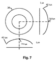
図7は、フラッシュのシミュレーション結果を示しており、ここで、全体の光束は360ルクス(lux)である。測定は、カメラレンズの焦点距離において行われており、スマートフォンのモデルに応じて、約10mmであり得る。示されるように、発光プロフィールは、水平および垂直に実質的に対称であって、中心において74ルクスであるピーク光束を伴い、カメラの視野のエッジにおいて約40ルクスまでロールオフ(rolling off)していて、たいてい被写体がフレームの中央に居るスマートフォンカメラのためにフラッシュが役立つようにしている。対角線上の均一性は、75度の視野については40%より大きいが、光抽出特徴56(図5)を調整することによって改善することができる。 FIG. 7 shows the simulation results of the flash, where the total luminous flux is 360 lux. The measurements are taken at the focal length of the camera lens and may be about 10 mm, depending on the model of the smartphone. As shown, the emission profile is substantially symmetrical horizontally and vertically, with a peak flux of 74 lux at the center, rolling off to about 40 lux at the edge of the camera field of view The flash is usually useful for smartphone cameras where the subject is in the middle of the frame. Diagonal uniformity can be improved by adjusting the light extraction features 56 (FIG. 5), although greater than 40% for a 75 degree field of view.
特定的な実施形態が示され、かつ、説明されてきたが、当業者にとっては、より広範な態様において、本開示から逸脱することなく変更および変形を行うことができること、そして、従って、添付の請求項は、本開示の真の精神および範囲内にあるそうした変更および変形の全てをその範囲内に包含すること、が明らかであろう。 While specific embodiments have been shown and described, those of ordinary skill in the art will be able to make modifications and variations in a broader aspect without departing from the present disclosure and, therefore, attached. It will be apparent that the claims encompass within their scope all such changes and modifications that are within the true spirit and scope of the present disclosure.
Claims (17)
中央開口部を有するリングとして形成された光ガイドであり、該光ガイドの光排出面上に光抽出特徴を有している、光ガイドと、
第1コンダクタを含む第1プリント回路基板であり、第1発光ダイオード(LED)を前記第1コンダクタに対して電気的に接続するための第1表面を有している、第1プリント回路基板と、
前記第1表面上にマウントされ、かつ、前記第1コンダクタに対して電気的に接続されている第1LEDと、を含み、
前記第1プリント回路基板の少なくとも第1部分および前記第1LEDの全てが、前記光ガイドにおいてカプセル化されており、
前記第1プリント回路基板の第2部分が、電源に対して接続されるために前記光ガイドから延びており、かつ、
前記光ガイドは、前記光排出面を通じて放射されるまで、前記第1LEDからの光を、前記光ガイドの中で内部反射するように構成されている、
システム。 A flash system,
A light guide formed as a ring with a central opening, the light guide having light extraction features on the light exit surface of the light guide;
A first printed circuit board including a first conductor, the first printed circuit board having a first surface for electrically connecting a first light emitting diode (LED) to the first conductor; ,
And a first LED mounted on the first surface and electrically connected to the first conductor,
At least a first portion of the first printed circuit board and all of the first LEDs are encapsulated in the light guide,
A second portion of the first printed circuit board extends from the light guide for connection to a power supply, and
The light guide is configured to internally reflect light from the first LED into the light guide until it is emitted through the light exit surface.
system.
前記中央開口部の中または後方に置かれたカメラレンズ、を含む、
請求項1に記載のシステム。 The system further comprises
A camera lens located in or behind the central opening;
The system of claim 1.
第2コンダクタを含む第2プリント回路基板であり、第2LEDを前記第2コンダクタに対して電気的に接続するための第2表面を有している、第2プリント回路基板と、
前記第2表面上にマウントされ、かつ、前記第2コンダクタに対して電気的に接続されている第2LEDと、を含み、
前記第2プリント回路基板の少なくとも第1部分および前記第2LEDの全てが、前記光ガイドにおいてカプセル化されており、
前記第2プリント回路基板の第2部分が、前記電源に対して接続されるために前記光ガイドから延びており、
前記光ガイドは、被写体を照明するために前記光排出面を通じて放射されるまで、前記第1LEDおよび前記第2LEDからの光を、内部反射するように構成されており、
前記第2プリント回路基板の第2背面は、前記第1LEDからの光を反射するように構成されており、かつ、
前記第1プリント回路基板の第1背面は、前記第2LEDからの光を反射するように構成されている、
請求項1に記載のシステム。 The system further comprises
A second printed circuit board comprising a second conductor, the second printed circuit board having a second surface for electrically connecting a second LED to the second conductor;
And a second LED mounted on the second surface and electrically connected to the second conductor,
At least a first portion of the second printed circuit board and all the second LEDs are encapsulated in the light guide,
A second portion of the second printed circuit board extends from the light guide for connection to the power supply,
The light guide is configured to internally reflect light from the first LED and the second LED until emitted through the light exit surface to illuminate the subject.
The second backside of the second printed circuit board is configured to reflect light from the first LED, and
The first back side of the first printed circuit board is configured to reflect light from the second LED,
The system of claim 1.
前記第2プリント回路基板の前記第2背面は、第2拡散性白色表面である、
請求項3に記載のシステム。 The first back side of the first printed circuit board is a first diffuse white surface, and
The second backside of the second printed circuit board is a second diffuse white surface,
The system of claim 3.
前記第1プリント回路基板の前記第1表面は、前記光ガイドの前記光排出面に対して実質的に垂直であり、かつ、
前記第1プリント回路基板は、第1反射性背面を有している、
請求項1に記載のシステム。 The first LED is a top emission LED,
The first surface of the first printed circuit board is substantially perpendicular to the light exit surface of the light guide, and
The first printed circuit board has a first reflective back surface,
The system of claim 1.
前記第1プリント回路基板の前記第1表面は、前記光ガイドの前記光排出面に対して平行である、
請求項1に記載のシステム。 The first LED is a side emission LED, and
The first surface of the first printed circuit board is parallel to the light exit surface of the light guide.
The system of claim 1.
前記光ガイドにおいてカプセル化された、追加のLEDおよびプリント回路基板、を含む、
請求項1に記載のシステム。 The system further comprises
Including additional LEDs and printed circuit boards encapsulated in said light guide,
The system of claim 1.
当たっている光の異なる量を抽出するために、形状、サイズ、及び/又は、コンフィグレーションのうち1つまたはそれ以上が変動しており、前記光排出面の周囲から出て行く光が実質的に均一になるようにしている、
請求項1に記載のシステム。 The light extraction features on the light exit surface are:
One or more of the shape, size, and / or configuration may be varied to extract different amounts of impinging light, and the light exiting from the perimeter of the light emitting surface may be substantially To be uniform,
The system of claim 1.
請求項1に記載のシステム。 The emission profile of light emitted from the light exit surface has a peak substantially aligned with the axis of the central opening at a specific distance from the light guide and is remote from the central opening Rolled off,
The system of claim 1.
ハウジングと、
前記ハウジング上に配置されているフラッシュシステムと、
前記ハウジングの中に配置されているカメラと、
前記カメラに対して結合され、かつ、前記フラッシュシステムの光ガイドの中央開口部の中に配置されているカメラレンズと、を含み、
前記フラッシュシステムは、
前記中央開口部を有するリングとして形成された光ガイドであり、該光ガイドの光排出面上に光抽出特徴を有している、光ガイドと、
第1コンダクタを含む第1プリント回路基板であり、第1発光ダイオード(LED)を前記第1コンダクタに対して電気的に接続するための第1表面を有している、第1プリント回路基板と、
前記第1表面上にマウントされ、かつ、前記第1コンダクタに対して電気的に接続されている第1LEDと、を含み、
前記第1プリント回路基板の少なくとも第1部分および前記第1LEDの全てが、前記光ガイドにおいてカプセル化されており、
前記第1プリント回路基板の第2部分が、電源に対して接続されるために前記光ガイドから延びており、かつ、
前記光ガイドは、前記光排出面を通じて放射されるまで、前記第1LEDからの光を、前記光ガイドの中で内部反射するように構成されている、
電子機器。 An electronic device,
With the housing,
A flash system disposed on the housing;
A camera disposed in the housing;
A camera lens coupled to the camera and disposed in a central opening of a light guide of the flash system;
The flash system is
A light guide formed as a ring with the central opening, the light guide having light extraction features on the light exit surface of the light guide;
A first printed circuit board including a first conductor, the first printed circuit board having a first surface for electrically connecting a first light emitting diode (LED) to the first conductor; ,
And a first LED mounted on the first surface and electrically connected to the first conductor,
At least a first portion of the first printed circuit board and all of the first LEDs are encapsulated in the light guide,
A second portion of the first printed circuit board extends from the light guide for connection to a power supply, and
The light guide is configured to internally reflect light from the first LED into the light guide until it is emitted through the light exit surface.
Electronics.
第2コンダクタを含む第2プリント回路基板であり、第2LEDを前記第2コンダクタに対して電気的に接続するための第2表面を有している、第2プリント回路基板と、
前記第2表面上にマウントされ、かつ、前記第2コンダクタに対して電気的に接続されている第2LEDと、を含み、
前記第2プリント回路基板の少なくとも第1部分および前記第2LEDの全てが、前記光ガイドにおいてカプセル化されており、
前記第2プリント回路基板の第2部分が、前記電源に対して接続されるために前記光ガイドから延びており、
前記光ガイドは、被写体を照明するために前記光排出面を通じて放射されるまで、前記第1LEDおよび前記第2LEDからの光を、内部反射するように構成されており、
前記第2プリント回路基板の第2背面は、前記第1LEDからの光を反射するように構成されており、かつ、
前記第1プリント回路基板の第1背面は、前記第2LEDからの光を反射するように構成されている、
請求項1に記載の電子機器。 The flash system further comprises
A second printed circuit board comprising a second conductor, the second printed circuit board having a second surface for electrically connecting a second LED to the second conductor;
And a second LED mounted on the second surface and electrically connected to the second conductor,
At least a first portion of the second printed circuit board and all the second LEDs are encapsulated in the light guide,
A second portion of the second printed circuit board extends from the light guide for connection to the power supply,
The light guide is configured to internally reflect light from the first LED and the second LED until emitted through the light exit surface to illuminate the subject.
The second backside of the second printed circuit board is configured to reflect light from the first LED, and
The first back side of the first printed circuit board is configured to reflect light from the second LED,
The electronic device according to claim 1.
前記第2プリント回路基板の前記第2背面は、第2拡散性白色表面である、
請求項11に記載の電子機器。 The first back side of the first printed circuit board is a first diffuse white surface, and
The second backside of the second printed circuit board is a second diffuse white surface,
The electronic device according to claim 11.
前記第1プリント回路基板の前記第1表面は、前記光ガイドの前記光排出面に対して実質的に垂直であり、かつ、
前記第1プリント回路基板は、第1反射性背面を有している、
請求項10に記載の電子機器。 The first LED is a top emission LED,
The first surface of the first printed circuit board is substantially perpendicular to the light exit surface of the light guide, and
The first printed circuit board has a first reflective back surface,
The electronic device of Claim 10.
前記第1プリント回路基板の前記第1表面は、前記光ガイドの前記光排出面に対して平行である、
請求項10に記載の電子機器。 The first LED is a side emission LED, and
The first surface of the first printed circuit board is parallel to the light exit surface of the light guide.
The electronic device of Claim 10.
前記光ガイドにおいてカプセル化された、追加のLEDおよびプリント回路基板、を含む、
請求項10に記載の電子機器。 The flash system further comprises
Including additional LEDs and printed circuit boards encapsulated in said light guide,
The electronic device of Claim 10.
当たっている光の異なる量を抽出するために、形状、サイズ、及び/又は、コンフィグレーションのうち1つまたはそれ以上が変動しており、前記光排出面の周囲から出て行く光が実質的に均一になるようにしている、
請求項10に記載の電子機器。 The light extraction features on the light exit surface are:
One or more of the shape, size, and / or configuration may be varied to extract different amounts of impinging light, and the light exiting from the perimeter of the light emitting surface may be substantially To be uniform,
The electronic device of Claim 10.
請求項10に記載の電子機器。 The emission profile of light emitted from the light exit surface has a peak substantially aligned with the axis of the central opening at a specific distance from the light guide and is remote from the central opening Rolled off,
The electronic device of Claim 10.
Priority Applications (1)
| Application Number | Priority Date | Filing Date | Title |
|---|---|---|---|
| JP2021123895A JP7162105B2 (en) | 2016-04-26 | 2021-07-29 | LED flash ring that surrounds the camera lens |
Applications Claiming Priority (5)
| Application Number | Priority Date | Filing Date | Title |
|---|---|---|---|
| US201662327628P | 2016-04-26 | 2016-04-26 | |
| US62/327,628 | 2016-04-26 | ||
| EP16173241.7 | 2016-06-07 | ||
| EP16173241 | 2016-06-07 | ||
| PCT/US2017/029522 WO2017189653A1 (en) | 2016-04-26 | 2017-04-26 | Led flash ring surrounding camera lens |
Related Child Applications (1)
| Application Number | Title | Priority Date | Filing Date |
|---|---|---|---|
| JP2021123895A Division JP7162105B2 (en) | 2016-04-26 | 2021-07-29 | LED flash ring that surrounds the camera lens |
Publications (2)
| Publication Number | Publication Date |
|---|---|
| JP2019519803A true JP2019519803A (en) | 2019-07-11 |
| JP2019519803A5 JP2019519803A5 (en) | 2020-06-11 |
Family
ID=67222992
Family Applications (2)
| Application Number | Title | Priority Date | Filing Date |
|---|---|---|---|
| JP2018555901A Pending JP2019519803A (en) | 2016-04-26 | 2017-04-26 | LED flash ring surrounding the camera lens |
| JP2021123895A Active JP7162105B2 (en) | 2016-04-26 | 2021-07-29 | LED flash ring that surrounds the camera lens |
Family Applications After (1)
| Application Number | Title | Priority Date | Filing Date |
|---|---|---|---|
| JP2021123895A Active JP7162105B2 (en) | 2016-04-26 | 2021-07-29 | LED flash ring that surrounds the camera lens |
Country Status (3)
| Country | Link |
|---|---|
| US (2) | US10558107B2 (en) |
| JP (2) | JP2019519803A (en) |
| TW (1) | TWI760955B (en) |
Cited By (1)
| Publication number | Priority date | Publication date | Assignee | Title |
|---|---|---|---|---|
| US10845677B2 (en) | 2016-04-26 | 2020-11-24 | Lumileds Llc | LED flash ring surrounding camera lens |
Families Citing this family (2)
| Publication number | Priority date | Publication date | Assignee | Title |
|---|---|---|---|---|
| US11131904B2 (en) | 2019-10-16 | 2021-09-28 | Xavier DeLaPaz | Photographic light generating panel |
| CN113364958B (en) * | 2019-12-25 | 2022-12-27 | Oppo广东移动通信有限公司 | Light guide part applied to camera assembly |
Citations (6)
| Publication number | Priority date | Publication date | Assignee | Title |
|---|---|---|---|---|
| JP2004226508A (en) * | 2003-01-21 | 2004-08-12 | Fuji Photo Film Co Ltd | Illuminator, electronic flash device for camera and camera |
| JP2005019874A (en) * | 2003-06-27 | 2005-01-20 | Matsushita Electric Ind Co Ltd | Led, led chip, led module, and lighting system |
| JP2006236974A (en) * | 2005-01-28 | 2006-09-07 | Toyoda Gosei Co Ltd | Ring-shaped light emitting unit |
| JP2007174168A (en) * | 2005-12-21 | 2007-07-05 | Soken:Kk | Automatic photographing output device |
| WO2007099860A1 (en) * | 2006-02-23 | 2007-09-07 | Matsushita Electric Works, Ltd. | Led illumination device |
| JP2011118383A (en) * | 2009-11-26 | 2011-06-16 | Sharp Corp | Flash, camera, and method of generating flash |
Family Cites Families (26)
| Publication number | Priority date | Publication date | Assignee | Title |
|---|---|---|---|---|
| CH691333A5 (en) | 1997-02-19 | 2001-06-29 | Asulab Sa | Device for uniform illumination of the dial of a display device. |
| JP4636914B2 (en) * | 2005-03-16 | 2011-02-23 | キヤノン株式会社 | Light emitting device |
| JP4579729B2 (en) * | 2005-03-18 | 2010-11-10 | キヤノン株式会社 | Light emitting device |
| CZ200644A3 (en) | 2006-01-23 | 2007-09-19 | Short Images, S. R. O. | Circular speed lamp |
| GB2438440B (en) * | 2006-05-26 | 2008-04-23 | Design Led Products Ltd | A composite light guiding device |
| WO2008042351A2 (en) * | 2006-10-02 | 2008-04-10 | Illumitex, Inc. | Led system and method |
| DE102007033455B4 (en) | 2007-07-18 | 2009-06-25 | Bron Elektronik Ag | Lighting device for the flash photography |
| US7712907B2 (en) * | 2008-03-19 | 2010-05-11 | Zyka Dalibor | Ring flash adapter |
| WO2011019785A1 (en) * | 2009-08-12 | 2011-02-17 | 3M Innovative Properties Company | Lightguide |
| CN102483798B (en) * | 2009-10-30 | 2015-01-28 | 富士通先端科技株式会社 | Illumination optical system of image capturing device |
| US8783915B2 (en) * | 2010-02-11 | 2014-07-22 | Bridgelux, Inc. | Surface-textured encapsulations for use with light emitting diodes |
| JP4975136B2 (en) * | 2010-04-13 | 2012-07-11 | シャープ株式会社 | Lighting device |
| JP4844680B2 (en) * | 2010-05-25 | 2011-12-28 | パナソニック株式会社 | Lighting device and camera |
| KR101830670B1 (en) | 2011-06-27 | 2018-02-21 | 엘지전자 주식회사 | Mobile terminal |
| TWM435624U (en) * | 2011-11-10 | 2012-08-11 | Yang-Shan Yeh | Flashlight structure for camera function of handheld electronic device |
| GB2498347A (en) * | 2012-01-10 | 2013-07-17 | Design Led Products Ltd | A lighting panel with side mounted top emitting LEDs |
| CN103369083A (en) | 2012-04-11 | 2013-10-23 | 上海昌域投资管理有限公司 | Cellphone OLED annular flash lamp |
| CN202794796U (en) | 2012-07-10 | 2013-03-13 | 欧司朗股份有限公司 | Annular flashlight and mobile phone with the annular flashlight |
| CN104977778B (en) * | 2014-04-02 | 2018-02-27 | 神讯电脑(昆山)有限公司 | Flash lamp hides ring structure and its manufacture method |
| CN203894516U (en) | 2014-03-04 | 2014-10-22 | 蔡思强 | Non-detachable annular flash lamp suitable for mobile terminal |
| CN106662750B (en) * | 2015-02-17 | 2021-03-12 | 奥斯特豪特集团有限公司 | See-through computer display system |
| CN107924030A (en) * | 2015-08-26 | 2018-04-17 | 3M创新有限公司 | Collimate light guide |
| CN107949801A (en) * | 2015-08-26 | 2018-04-20 | 3M创新有限公司 | Collimate ladder wedge light guide |
| US10288983B2 (en) | 2016-04-26 | 2019-05-14 | Lumileds Llc | LED flash ring surrounding camera lens |
| TWI760955B (en) * | 2016-04-26 | 2022-04-11 | 荷蘭商露明控股公司 | Led flash ring surrounding camera lens and methods for providing illumination |
| US10288986B2 (en) * | 2017-02-22 | 2019-05-14 | Trw Automotive U.S. Llc | Moderation of a driver assist camera enhancement via a vehicle windshield |
-
2017
- 2017-04-26 TW TW109143004A patent/TWI760955B/en active
- 2017-04-26 JP JP2018555901A patent/JP2019519803A/en active Pending
-
2019
- 2019-03-29 US US16/369,588 patent/US10558107B2/en active Active
- 2019-12-31 US US16/731,779 patent/US10845677B2/en active Active
-
2021
- 2021-07-29 JP JP2021123895A patent/JP7162105B2/en active Active
Patent Citations (6)
| Publication number | Priority date | Publication date | Assignee | Title |
|---|---|---|---|---|
| JP2004226508A (en) * | 2003-01-21 | 2004-08-12 | Fuji Photo Film Co Ltd | Illuminator, electronic flash device for camera and camera |
| JP2005019874A (en) * | 2003-06-27 | 2005-01-20 | Matsushita Electric Ind Co Ltd | Led, led chip, led module, and lighting system |
| JP2006236974A (en) * | 2005-01-28 | 2006-09-07 | Toyoda Gosei Co Ltd | Ring-shaped light emitting unit |
| JP2007174168A (en) * | 2005-12-21 | 2007-07-05 | Soken:Kk | Automatic photographing output device |
| WO2007099860A1 (en) * | 2006-02-23 | 2007-09-07 | Matsushita Electric Works, Ltd. | Led illumination device |
| JP2011118383A (en) * | 2009-11-26 | 2011-06-16 | Sharp Corp | Flash, camera, and method of generating flash |
Cited By (1)
| Publication number | Priority date | Publication date | Assignee | Title |
|---|---|---|---|---|
| US10845677B2 (en) | 2016-04-26 | 2020-11-24 | Lumileds Llc | LED flash ring surrounding camera lens |
Also Published As
| Publication number | Publication date |
|---|---|
| TWI760955B (en) | 2022-04-11 |
| JP2021182147A (en) | 2021-11-25 |
| US20190265576A1 (en) | 2019-08-29 |
| JP7162105B2 (en) | 2022-10-27 |
| US20200133094A1 (en) | 2020-04-30 |
| TW202122900A (en) | 2021-06-16 |
| US10845677B2 (en) | 2020-11-24 |
| US10558107B2 (en) | 2020-02-11 |
Similar Documents
| Publication | Publication Date | Title |
|---|---|---|
| JP7162105B2 (en) | LED flash ring that surrounds the camera lens | |
| TWI231611B (en) | Light-emitting diode | |
| US10288983B2 (en) | LED flash ring surrounding camera lens | |
| US8033691B2 (en) | LED lamp producing sparkle | |
| JP5264650B2 (en) | LED lighting device | |
| US20140084809A1 (en) | Variable-beam light source and related methods | |
| TWI386748B (en) | Camera with an array of light emitting diode (LED) flash | |
| CN207527398U (en) | A kind of light compensating lamp and video camera | |
| JP6624550B2 (en) | lighting equipment | |
| KR20130003835A (en) | Camera flash module | |
| TWM507489U (en) | Ring-shaped light-emitting device | |
| JP6956110B2 (en) | Lighting device | |
| CN211786206U (en) | Light guide element, light assembly and electronic equipment | |
| KR101273364B1 (en) | Substrate for fabricating led module, and led module using the same, and method for fabricating the led module | |
| CN210639401U (en) | Flash lamp based on semiconductor laser | |
| CN212989696U (en) | Flash lamp lens | |
| WO2019105059A1 (en) | Fill light and camera | |
| JP2018073792A (en) | Luminaire and display | |
| KR20150065502A (en) | Lighting module | |
| CN104048193B (en) | Led lamp bead | |
| KR20110092756A (en) | Led flash unit with reflector | |
| TWI414871B (en) | Portable electronic device and flashlight module | |
| KR20170014288A (en) | Lens and lens module using the same | |
| JP2016126973A (en) | Luminaire and monitoring system | |
| TW201224363A (en) | Light-guide type illumination device |
Legal Events
| Date | Code | Title | Description |
|---|---|---|---|
| A521 | Request for written amendment filed |
Free format text: JAPANESE INTERMEDIATE CODE: A523 Effective date: 20181227 |
|
| A521 | Request for written amendment filed |
Free format text: JAPANESE INTERMEDIATE CODE: A523 Effective date: 20200423 |
|
| A621 | Written request for application examination |
Free format text: JAPANESE INTERMEDIATE CODE: A621 Effective date: 20200423 |
|
| A871 | Explanation of circumstances concerning accelerated examination |
Free format text: JAPANESE INTERMEDIATE CODE: A871 Effective date: 20200423 |
|
| A975 | Report on accelerated examination |
Free format text: JAPANESE INTERMEDIATE CODE: A971005 Effective date: 20200629 |
|
| A131 | Notification of reasons for refusal |
Free format text: JAPANESE INTERMEDIATE CODE: A131 Effective date: 20200707 |
|
| A521 | Request for written amendment filed |
Free format text: JAPANESE INTERMEDIATE CODE: A523 Effective date: 20201005 |
|
| A131 | Notification of reasons for refusal |
Free format text: JAPANESE INTERMEDIATE CODE: A131 Effective date: 20201110 |
|
| A521 | Request for written amendment filed |
Free format text: JAPANESE INTERMEDIATE CODE: A523 Effective date: 20210201 |
|
| A02 | Decision of refusal |
Free format text: JAPANESE INTERMEDIATE CODE: A02 Effective date: 20210330 |