JP2017538215A - Instructions and logic to perform reverse separation operation - Google Patents
Instructions and logic to perform reverse separation operation Download PDFInfo
- Publication number
- JP2017538215A JP2017538215A JP2017527276A JP2017527276A JP2017538215A JP 2017538215 A JP2017538215 A JP 2017538215A JP 2017527276 A JP2017527276 A JP 2017527276A JP 2017527276 A JP2017527276 A JP 2017527276A JP 2017538215 A JP2017538215 A JP 2017538215A
- Authority
- JP
- Japan
- Prior art keywords
- register
- instruction
- field
- bit
- operand
- Prior art date
- Legal status (The legal status is an assumption and is not a legal conclusion. Google has not performed a legal analysis and makes no representation as to the accuracy of the status listed.)
- Ceased
Links
- 238000000926 separation method Methods 0.000 title claims abstract description 46
- 230000002441 reversible effect Effects 0.000 title claims abstract description 34
- 238000012545 processing Methods 0.000 claims abstract description 44
- 238000000034 method Methods 0.000 claims description 27
- 238000004519 manufacturing process Methods 0.000 claims description 3
- 230000015654 memory Effects 0.000 description 133
- VOXZDWNPVJITMN-ZBRFXRBCSA-N 17β-estradiol Chemical compound OC1=CC=C2[C@H]3CC[C@](C)([C@H](CC4)O)[C@@H]4[C@@H]3CCC2=C1 VOXZDWNPVJITMN-ZBRFXRBCSA-N 0.000 description 77
- 238000010586 diagram Methods 0.000 description 50
- 238000006073 displacement reaction Methods 0.000 description 40
- 238000007667 floating Methods 0.000 description 34
- 238000006243 chemical reaction Methods 0.000 description 17
- 230000006870 function Effects 0.000 description 16
- 239000000872 buffer Substances 0.000 description 11
- 230000008569 process Effects 0.000 description 10
- 101000912503 Homo sapiens Tyrosine-protein kinase Fgr Proteins 0.000 description 8
- 102100026150 Tyrosine-protein kinase Fgr Human genes 0.000 description 8
- 238000004891 communication Methods 0.000 description 8
- 239000003795 chemical substances by application Substances 0.000 description 7
- 238000005516 engineering process Methods 0.000 description 7
- 238000004364 calculation method Methods 0.000 description 6
- 230000000295 complement effect Effects 0.000 description 5
- 230000006835 compression Effects 0.000 description 5
- 238000007906 compression Methods 0.000 description 5
- 230000007246 mechanism Effects 0.000 description 5
- 238000013519 translation Methods 0.000 description 5
- 230000008859 change Effects 0.000 description 4
- 230000003068 static effect Effects 0.000 description 4
- 238000012546 transfer Methods 0.000 description 4
- 230000008901 benefit Effects 0.000 description 3
- 238000004590 computer program Methods 0.000 description 3
- 230000001419 dependent effect Effects 0.000 description 3
- 238000013461 design Methods 0.000 description 3
- 230000036961 partial effect Effects 0.000 description 3
- 230000002829 reductive effect Effects 0.000 description 3
- 241000283707 Capra Species 0.000 description 2
- 241001494479 Pecora Species 0.000 description 2
- 101000579490 Solanum lycopersicum Suberization-associated anionic peroxidase 1 Proteins 0.000 description 2
- 101001073211 Solanum lycopersicum Suberization-associated anionic peroxidase 2 Proteins 0.000 description 2
- 230000008878 coupling Effects 0.000 description 2
- 238000010168 coupling process Methods 0.000 description 2
- 238000005859 coupling reaction Methods 0.000 description 2
- 230000003287 optical effect Effects 0.000 description 2
- 230000001629 suppression Effects 0.000 description 2
- 101100285899 Saccharomyces cerevisiae (strain ATCC 204508 / S288c) SSE2 gene Proteins 0.000 description 1
- 238000013459 approach Methods 0.000 description 1
- 238000003491 array Methods 0.000 description 1
- 230000006399 behavior Effects 0.000 description 1
- 239000002131 composite material Substances 0.000 description 1
- 150000001875 compounds Chemical class 0.000 description 1
- 238000010276 construction Methods 0.000 description 1
- 238000002955 isolation Methods 0.000 description 1
- 230000014759 maintenance of location Effects 0.000 description 1
- 230000000873 masking effect Effects 0.000 description 1
- 238000012986 modification Methods 0.000 description 1
- 230000004048 modification Effects 0.000 description 1
- 239000013642 negative control Substances 0.000 description 1
- 229910052754 neon Inorganic materials 0.000 description 1
- GKAOGPIIYCISHV-UHFFFAOYSA-N neon atom Chemical compound [Ne] GKAOGPIIYCISHV-UHFFFAOYSA-N 0.000 description 1
- 238000005192 partition Methods 0.000 description 1
- 230000002093 peripheral effect Effects 0.000 description 1
- 239000004065 semiconductor Substances 0.000 description 1
- 238000004088 simulation Methods 0.000 description 1
- 239000000758 substrate Substances 0.000 description 1
Images


Classifications
-
- G—PHYSICS
- G06—COMPUTING; CALCULATING OR COUNTING
- G06F—ELECTRIC DIGITAL DATA PROCESSING
- G06F9/00—Arrangements for program control, e.g. control units
- G06F9/06—Arrangements for program control, e.g. control units using stored programs, i.e. using an internal store of processing equipment to receive or retain programs
- G06F9/30—Arrangements for executing machine instructions, e.g. instruction decode
- G06F9/30181—Instruction operation extension or modification
- G06F9/30185—Instruction operation extension or modification according to one or more bits in the instruction, e.g. prefix, sub-opcode
-
- G—PHYSICS
- G06—COMPUTING; CALCULATING OR COUNTING
- G06F—ELECTRIC DIGITAL DATA PROCESSING
- G06F7/00—Methods or arrangements for processing data by operating upon the order or content of the data handled
- G06F7/76—Arrangements for rearranging, permuting or selecting data according to predetermined rules, independently of the content of the data
- G06F7/764—Masking
-
- G—PHYSICS
- G06—COMPUTING; CALCULATING OR COUNTING
- G06F—ELECTRIC DIGITAL DATA PROCESSING
- G06F9/00—Arrangements for program control, e.g. control units
- G06F9/06—Arrangements for program control, e.g. control units using stored programs, i.e. using an internal store of processing equipment to receive or retain programs
- G06F9/30—Arrangements for executing machine instructions, e.g. instruction decode
- G06F9/30003—Arrangements for executing specific machine instructions
- G06F9/30007—Arrangements for executing specific machine instructions to perform operations on data operands
- G06F9/30018—Bit or string instructions
-
- G—PHYSICS
- G06—COMPUTING; CALCULATING OR COUNTING
- G06F—ELECTRIC DIGITAL DATA PROCESSING
- G06F9/00—Arrangements for program control, e.g. control units
- G06F9/06—Arrangements for program control, e.g. control units using stored programs, i.e. using an internal store of processing equipment to receive or retain programs
- G06F9/30—Arrangements for executing machine instructions, e.g. instruction decode
- G06F9/30003—Arrangements for executing specific machine instructions
- G06F9/30007—Arrangements for executing specific machine instructions to perform operations on data operands
- G06F9/30032—Movement instructions, e.g. MOVE, SHIFT, ROTATE, SHUFFLE
Abstract
1つの実施形態では、ベクトルレジスタ又は汎用レジスタを用いて逆分離演算を実行するために、処理デバイスが命令のセットを実行する。逆分離演算は、ソースの両領域のビットをインターリーブし、インターリーブされたビットをデスティネーションに書き込む。命令は制御マスクを用い、1のマスク値を有する各ビットがソースレジスタの一方側から取得される、又はゼロのマスクを有するベクトル要素が反対側から取得される。In one embodiment, the processing device performs a set of instructions to perform reverse separation operations using vector registers or general purpose registers. The reverse separation operation interleaves the bits in both regions of the source and writes the interleaved bits to the destination. The instruction uses a control mask and each bit with a mask value of 1 is taken from one side of the source register, or a vector element with a mask of zero is taken from the other side.
Description
本開示は、処理ロジック、マイクロプロセッサ、及び関連する命令セットアーキテクチャの分野に関し、これらはプロセッサ又は他の処理ロジックにより実行される場合、論理的演算、数学的演算、又は他の関数的演算を実行する。 The present disclosure relates to the field of processing logic, microprocessors, and related instruction set architectures, which perform logical, mathematical, or other functional operations when performed by a processor or other processing logic. To do.
特定のタイプのアプリケーションは、同じ演算が多数のデータ項目に対して実行される必要があることが多い(「データ並列処理」と呼ばれる)。単一命令・複数データ処理(SIMD)は、ある演算を複数のデータ項目に対してプロセッサに実行させる命令の一種を指す。SIMD技術は特に、レジスタ中のビットを論理的に複数の固定サイズデータ要素(それぞれが別個の値を表す)に分割し得るプロセッサに適している。例えば、256ビットレジスタ中のビットは、4個の別個の64ビットパックドデータ要素(クワッドワード(Q)サイズのデータ要素)、8個の別個の32ビットパックドデータ要素(ダブルワード(D)サイズのデータ要素)、16個の別個の16ビットパックドデータ要素(ワード(W)サイズのデータ要素)、又は32個の別個の8ビットデータ要素(バイト(B)サイズのデータ要素)として処理されるソースオペランドに指定されてよい。このタイプのデータは「パックド」データタイプ又は「ベクトル」データタイプと呼ばれ、このデータタイプのオペランドは、パックドデータオペランド又はベクトルオペランドと呼ばれる。換言すると、パックドデータ項目又はベクトルは、一連のパックドデータ要素を意味し、パックドデータオペランド又はベクトルオペランドは、SIMD命令のソースオペランド又はデスティネーションオペランドである(パックドデータ命令又はベクトル命令としても知られる)。 Certain types of applications often require the same operation to be performed on multiple data items (referred to as “data parallelism”). Single instruction / multiple data processing (SIMD) refers to a type of instruction that causes a processor to perform a certain operation on a plurality of data items. SIMD technology is particularly suitable for processors that can logically divide the bits in a register into a plurality of fixed size data elements, each representing a distinct value. For example, a bit in a 256-bit register consists of four separate 64-bit packed data elements (quadword (Q) size data elements), eight separate 32-bit packed data elements (double word (D) size) Data element), 16 separate 16-bit packed data elements (word (W) size data elements), or 32 separate 8-bit data elements (byte (B) size data elements) It may be specified as an operand. This type of data is referred to as a “packed” data type or “vector” data type, and operands of this data type are referred to as packed data operands or vector operands. In other words, a packed data item or vector means a series of packed data elements, and the packed data operand or vector operand is the source or destination operand of a SIMD instruction (also known as a packed data instruction or vector instruction). .
実施形態が、添付図面の図に限定するのではなく、例として示される。 The embodiments are shown by way of example and not by way of limitation to the figures of the accompanying drawings.
x86、MMX(登録商標)、ストリーミングSIMD拡張(SSE)、SSE2、SSE3、SSE4.1、及びSSE4.2命令を含む命令セットを搭載したIntel(登録商標)Core(登録商標)プロセッサによって利用されるなど、SIMD技術はアプリケーション性能の著しい改善を可能にした。アドバンスト・ベクトル・エクステンション(AVX)(AVX1及びAVX2)と呼ばれ、ベクトル拡張(VEX)コード体系を用いるSIMD拡張の追加セットが公開されている(例えば、Intel(登録商標)64及びIA−32アーキテクチャ・ソフトウェア・デベロッパーズ・マニュアル(2014年9月)、及びIntel(登録商標)アーキテクチャ命令セット拡張プログラミング・リファレンス(2014年9月)を参照)。Intel(登録商標)アーキテクチャ(IA)を拡張するアーキテクチャ拡張が説明されている。しかし、基本原理は、いかなる特定のISAにも限定されてはいない。 Used by Intel® Core® processor with instruction set including x86, MMX®, Streaming SIMD Extension (SSE), SSE2, SSE3, SSE4.1, and SSE4.2 instructions SIMD technology has enabled significant improvements in application performance. Called Advanced Vector Extension (AVX) (AVX1 and AVX2), an additional set of SIMD extensions using the Vector Extension (VEX) coding scheme is published (eg, Intel® 64 and IA-32 architectures) (See Software Developers Manual (September 2014) and Intel® Architecture Instruction Set Extended Programming Reference (September 2014)). An architecture extension is described that extends the Intel® Architecture (IA). However, the basic principle is not limited to any particular ISA.
1つの実施形態では、ベクトルレジスタ又は汎用レジスタを用いて逆分離演算を実行するために、処理デバイスが命令のセットを実行する。逆分離演算は、ソースの両領域のビットをインターリーブし、インターリーブされたビットをデスティネーションに書き込む。命令は制御マスクを用い、1のマスク値を有する各ビットがソースレジスタ又はベクトル要素の一方側から取得され、ゼロのマスクを有するビットが反対側から取得される。逆分離命令は、多くのビット操作ルーチンの構成要素である基本機能を実装するのに用いられてよい。 In one embodiment, the processing device performs a set of instructions to perform reverse separation operations using vector registers or general purpose registers. The reverse separation operation interleaves the bits in both regions of the source and writes the interleaved bits to the destination. The instruction uses a control mask, each bit having a mask value of 1 is taken from one side of the source register or vector element, and a bit having a mask of zero is taken from the other side. The reverse separation instruction may be used to implement a basic function that is a component of many bit manipulation routines.
本明細書で説明される実施形態に従い、プロセッサコアのアーキテクチャが以下に説明され、その後に例示的なプロセッサ及びコンピュータアーキテクチャの説明が続く。後述される本発明の実施形態について完全な理解を提供するために、多くの具体的な詳細が明記されている。しかし、これらの具体的な詳細の一部がなくても、実施形態は実施され得ることが当業者には明らかであろう。他の例では、様々な実施形態の基本原理をあいまいにしないように、周知の構造及びデバイスがブロック図の形式で示されている。 In accordance with the embodiments described herein, the architecture of the processor core is described below, followed by a description of exemplary processor and computer architectures. Numerous specific details are set forth in order to provide a thorough understanding of the embodiments of the invention described below. However, it will be apparent to one skilled in the art that the embodiments may be practiced without some of these specific details. In other instances, well-known structures and devices are shown in block diagram form in order to avoid obscuring the basic principles of the various embodiments.
プロセッサコアは、異なる方法で、異なる目的のために異なるプロセッサに実装されてよい。例えば、そのようなコアの実装は、1)汎用計算を対象とした汎用インオーダコア、2)汎用計算を対象とした高性能汎用アウトオブオーダコア、3)グラフィックス及び/又は科学(スループット)計算を主に対象とした専用コアを含んでよい。プロセッサは、単一のプロセッサコアを用いて実装されてよく、又は複数のプロセッサコアを含むこともできる。プロセッサ内の複数のプロセッサコアは、アーキテクチャ命令セットに関して同種でも異種でもよい。 The processor core may be implemented on different processors for different purposes in different ways. For example, the implementation of such a core can be: 1) general purpose in-order core for general purpose computation, 2) high performance general purpose out-of-order core for general purpose computation, 3) graphics and / or scientific (throughput) computation. It may include a dedicated core that is primarily targeted. A processor may be implemented using a single processor core or may include multiple processor cores. Multiple processor cores within a processor may be homogeneous or heterogeneous with respect to the architecture instruction set.
異なるプロセッサの実装は、1)汎用計算用の1つ又は複数の汎用インオーダコア、及び/又は、汎用計算を対象とした1つ又は複数の汎用アウトオブオーダコアを含む中央処理装置、並びに2)グラフィックス及び/又は科学的な用途を主に対象とした1つ又は複数の専用コア(例えば、多くの統合コアプロセッサ)を含むコプロセッサを含む。そのような異なるプロセッサによって異なるコンピュータシステムアーキテクチャがもたらされ、そこには次のものが含まれる。つまり、1)中央システムプロセッサとは別個のチップに搭載されたコプロセッサ、2)中央システムプロセッサと同じパッケージ内の別個のダイに搭載されたコプロセッサ、3)他のプロセッサコアと同じダイに搭載されたコプロセッサ(この場合、そのようなコプロセッサは統合グラフィックスロジック及び/又は科学(スループット)ロジックなどの専用ロジック、又は専用コアと呼ばれることがある)、及び4)説明されたプロセッサ(アプリケーションコア又はアプリケーションプロセッサと呼ばれることがある)、上述のコプロセッサ、及び追加機能を同じダイ上に含み得るシステムオンチップである。
[例示的なコアアーキテクチャ]
[インオーダコア及びアウトオブオーダコアのブロック図]
Different processor implementations include: 1) a central processing unit including one or more general purpose in-order cores for general purpose computations and / or one or more general purpose out-of-order cores intended for general purpose computations; and 2) graphics. Including a coprocessor that includes one or more dedicated cores (e.g., many integrated core processors) that are primarily intended for use in the field and / or scientific applications. Such different processors provide different computer system architectures, including: In other words, 1) a coprocessor mounted on a separate chip from the central system processor, 2) a coprocessor mounted on a separate die in the same package as the central system processor, and 3) mounted on the same die as other processor cores Coprocessors (in which case such coprocessors may be referred to as dedicated logic, such as integrated graphics logic and / or scientific (throughput) logic, or dedicated cores), and 4) the described processor (application System-on-chip, which may include the above-described coprocessor, and additional functions on the same die.
[Example core architecture]
[Block diagram of in-order core and out-of-order core]
図1Aは、ある実施形態に従い、例示的なインオーダパイプライン及び例示的なレジスタリネーミング・アウトオブオーダ発行/実行パイプラインを示すブロック図である。図1Bは、ある実施形態に従い、プロセッサに含まれるインオーダアーキテクチャコアの例示的な実施形態と、例示的なレジスタリネーミング・アウトオブオーダ発行/実行アーキテクチャコアとの両方を示すブロック図である。図1A〜図1Bの実線で示されたボックスは、インオーダパイプライン及びインオーダコアを示す。一方、破線で示されたボックスの任意の追加は、レジスタリネーミング・アウトオブオーダ発行/実行パイプライン及びコアを示す。インオーダ態様はアウトオブオーダ態様のサブセットであると仮定して、アウトオブオーダ態様が説明される。 FIG. 1A is a block diagram illustrating an exemplary in-order pipeline and an exemplary register renaming out-of-order issue / execution pipeline, according to an embodiment. FIG. 1B is a block diagram illustrating both an exemplary embodiment of an in-order architecture core included in a processor and an exemplary register renaming out-of-order issue / execution architecture core in accordance with an embodiment. The boxes indicated by the solid lines in FIGS. 1A-1B indicate the in-order pipeline and the in-order core. On the other hand, any addition of boxes indicated by dashed lines indicates register renaming out-of-order issue / execution pipelines and cores. Assuming that the in-order aspect is a subset of the out-of-order aspect, the out-of-order aspect is described.
図1Aにおいて、プロセッサパイプライン100は、フェッチステージ102、レングス復号ステージ104、復号ステージ106、割り当てステージ108、リネーミングステージ110、スケジューリング(ディスパッチ又は発行としても知られる)ステージ112、レジスタ読み出し/メモリ読み出しステージ114、実行ステージ116、ライトバック/メモリ書き込みステージ118、例外処理ステージ122、及びコミットステージ124を含む。
In FIG. 1A, the processor pipeline 100 includes a fetch
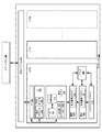
図1Bは、実行エンジンユニット150に結合されたフロントエンドユニット130を含むプロセッサコア190を示し、両方ともメモリユニット170に結合されている。コア190は、縮小命令セット計算(RISC)コア、複合命令セット計算(CISC)コア、超長命令語(VLIW)コア、あるいはハイブリッド又は代替的なコアタイプであってよい。さらに別の選択肢として、コア190は、例えば、ネットワーク又は通信コア、圧縮エンジン、コプロセッサコア、汎用計算グラフィックス処理ユニット(GPGPU)コア、グラフィックスコアなどの専用コアであってもよい。
FIG. 1B shows a processor core 190 that includes a
フロントエンドユニット130は、命令キャッシュユニット134に結合された分岐予測ユニット132を含み、命令キャッシュユニット134は命令変換ルックアサイドバッファ(TLB)136に結合され、命令変換ルックアサイドバッファ(TLB)136は命令フェッチユニット138に結合され、命令フェッチユニット138は復号ユニット140に結合されている。復号ユニット140(又はデコーダ)は、複数の命令を復号し、1つ又は複数のマイクロオペレーション、マイクロコードエントリポイント、マイクロ命令、他の命令、又は他の制御信号を出力として生成し得る。これらは、元の命令から復号され、又は別の方法で元の命令を反映し、又は元の命令から導出される。復号ユニット140は、様々な異なるメカニズムを用いて実装されてよい。適切なメカニズムの例には、限定されないが、ルックアップテーブル、ハードウェア実装、プログラマブルロジックアレイ(PLA)、マイクロコードリードオンリメモリ(ROM)などが含まれる。1つの実施形態では、コア190は、特定のマクロ命令用のマイクロコードを(例えば、復号ユニット140の中に、そうでなければフロントエンドユニット130内に)格納するマイクロコードROM又は他の媒体を含む。復号ユニット140は、実行エンジンユニット150内のリネーム/アロケータユニット152に結合されている。
The
実行エンジンユニット150は、リタイアメントユニット154と、1つ又は複数のスケジューラユニット156のセットとに結合されたリネーム/アロケータユニット152を含む。スケジューラユニット156は、リザベーションステーション、中央命令ウィンドウなどを含む任意の数の異なるスケジューラを表す。スケジューラユニット156は、物理レジスタファイルユニット158に結合されている。物理レジスタファイルユニット158のそれぞれは、1つ又は複数の物理レジスタファイルを表し、そのそれぞれ異なる物理レジスタファイルは、スカラ整数、スカラ浮動小数点、パックド整数、パックド浮動小数点、ベクトル整数、ベクトル浮動小数点、ステータス(例えば、実行される次の命令のアドレスである命令ポインタ)など、1つ又は複数の異なるデータタイプを格納する。1つの実施形態では、物理レジスタファイルユニット158は、ベクトルレジスタユニット、書き込みマスクレジスタユニット、及びスカラレジスタユニットを含む。これらのレジスタユニットは、アーキテクチャ上のベクトルレジスタ、ベクトルマスクレジスタ、及び汎用レジスタを提供し得る。物理レジスタファイルユニット158は、リタイアメントユニット154によってオーバーラップされ、レジスタリネーミング及びアウトオブオーダ実行が実装され得る様々な方法を示す(例えば、リオーダバッファ及びリタイアメントレジスタファイルを用いる、フューチャファイル、履歴バッファ、及びリタイアメントレジスタファイルを用いる、並びにレジスタマップ及びレジスタのプールを用いるなど)。リタイアメントユニット154及び物理レジスタファイルユニット158は、実行クラスタ160に結合されている。実行クラスタ160は、1つ又は複数の実行ユニット162のセットと、1つ又は複数のメモリアクセスユニット164のセットとを含む。実行ユニット162は、様々な演算(例えば、シフト、加算、減算、乗算)を様々なタイプのデータ(例えば、スカラ浮動小数点、パックド整数、パックド浮動小数点、ベクトル整数、ベクトル浮動小数点)に実行してよい。いくつかの実施形態は、特定の機能又は機能のセットに専用の複数の実行ユニットを含んでよく、他の実施形態は、1つのみの実行ユニット、又は全ての機能を全て実行する複数の実行ユニットを含んでもよい。特定の実施形態は、特定のタイプのデータ/オペレーションに対して別個のパイプラインを形成するので、スケジューラユニット156、物理レジスタファイルユニット158、及び実行クラスタ160は、可能性として複数であると示されている(例えば、スカラ整数パイプライン、スカラ浮動小数点/パックド整数/パックド浮動小数点/ベクトル整数/ベクトル浮動小数点パイプライン、及び/又はメモリアクセスパイプラインはそれぞれ、独自のスケジューラユニット、物理レジスタファイルユニット、及び/又は実行クラスタを有し、別個のメモリアクセスパイプラインの場合には、このパイプラインの実行クラスタのみがメモリアクセスユニット164を有する特定の実施形態が実装される)。別個のパイプラインが用いられる場合、これらのパイプラインのうち1つ又は複数がアウトオブオーダ発行/実行であってよく、残りがインオーダであってもよいことも理解されるべきである。
Execution engine unit 150 includes a rename / allocator unit 152 coupled to a
メモリアクセスユニット164のセットがメモリユニット170に結合され、メモリユニット170は、レベル2(L2)キャッシュユニット176に結合されたデータキャッシュユニット174に結合されたデータTLBユニット172を含む。1つの例示的な実施形態において、メモリアクセスユニット164は、ロードユニット、ストアアドレスユニット、及びストアデータユニットを含んでよく、これらのそれぞれはメモリユニット170内のデータTLBユニット172に結合されている。命令キャッシュユニット134は、メモリユニット170内のレベル2(L2)キャッシュユニット176にさらに結合される。L2キャッシュユニット176は、1つ又は複数の他のレベルのキャッシュに結合され、最終的にはメインメモリに結合される。
A set of memory access units 164 is coupled to the memory unit 170, which includes a
例として、例示的なレジスタリネーミング・アウトオブオーダ発行/実行コアアーキテクチャは、パイプライン100を以下のように実装してよい。すなわち、1)命令フェッチ138がフェッチステージ102及びレングス復号ステージ104を実行する。2)復号ユニット140が復号ステージ106を実行する。3)リネーム/アロケータユニット152が割り当てステージ108及びリネーミングステージ110を実行する。4)スケジューラユニット156がスケジュールステージ112を実行する。5)物理レジスタファイルユニット158及びメモリユニット170がレジスタ読み出し/メモリ読み出しステージ114を実行する。実行クラスタ160が実行ステージ116を実行する。6)メモリユニット170及び物理レジスタファイルユニット158がライトバック/メモリ書き込みステージ118を実行する。7)様々なユニットが例外処理ステージ122に関与し得る。8)リタイアメントユニット154及び物理レジスタファイルユニット158がコミットステージ124を実行する。
By way of example, an exemplary register renaming out-of-order issue / execution core architecture may implement pipeline 100 as follows. 1) Instruction fetch 138 executes fetch
コア190は、本明細書で説明される命令を含む1つ又は複数の命令セット(例えば、x86命令セット(より新しいバージョンと共に追加されたいくつかの拡張を有する)、MIPS Technologies(カリフォルニア州/サニーベール)のMIPS命令セット、ARM Holdings(英国/ケンブリッジ)のARM(登録商標)命令セット(NEONなどの任意の追加拡張を有する))をサポートしてよい。1つの実施形態では、コア190はパックドデータ命令セット拡張(例えば、AVX1、AVX2など)をサポートするロジックを含み、多くのマルチメディアアプリケーションにより用いられるオペレーションがパックドデータを用いて実行されることを可能にする。 Core 190 includes one or more instruction sets (eg, x86 instruction set (with some extensions added with newer versions), MIPS Technologies (California / Sunny), including the instructions described herein. Vale) MIPS instruction set, ARM Holdings (Cambridge / UK) ARM® instruction set (with any additional extensions such as NEON)). In one embodiment, core 190 includes logic that supports packed data instruction set extensions (eg, AVX1, AVX2, etc.), allowing operations used by many multimedia applications to be performed using packed data. To.
コアはマルチスレッディング(オペレーション又はスレッドからなる2つ又はそれより多くの並列セットを実行)をサポートしてよく、タイムスライスマルチスレッディング、同時マルチスレッディング(物理コアが同時にマルチスレッディングしているスレッドのそれぞれに対して、単一の物理コアが論理コアを提供する)、又はこれらの組み合わせ(例えば、タイムスライスフェッチ及び復号、並びにそれ以降のIntel(登録商標)ハイパースレッディング・テクノロジーなどの同時マルチスレッディング)を含む様々な方法でサポートしてよいことが理解されるべきである。 The core may support multi-threading (running two or more parallel sets of operations or threads), time slice multi-threading, simultaneous multi-threading (for each thread that the physical core is multi-threading at the same time). Supported in a variety of ways, including one physical core provides a logical core), or a combination of these (eg, simultaneous multithreading such as time slice fetch and decode, and later Intel® Hyper-Threading Technology) It should be understood that
レジスタリネーミングがアウトオブオーダ実行との関連で説明されるが、レジスタリネーミングはインオーダアーキテクチャで用いられてもよいことが理解されるべきである。示されたプロセッサの実施形態はまた、別々の命令キャッシュユニット134とデータキャッシュユニット174、並びに共有L2キャッシュユニット176を含むが、代替的な実施形態は、命令及びデータの両方に対して、例えばレベル1(L1)内部キャッシュ又は複数のレベルの内部キャッシュなど、単一の内部キャッシュを有してもよい。実施形態によっては、システムは、内部キャッシュ及び外部キャッシュの組み合わせを含んでよく、外部キャッシュはコア及び/又はプロセッサの外部に存在する。あるいは、全てのキャッシュが、コア及び/又はプロセッサの外部にあってもよい。
[具体的な例示的インオーダコアアーキテクチャ]
Although register renaming is described in the context of out-of-order execution, it should be understood that register renaming may be used in an in-order architecture. The illustrated processor embodiment also includes separate instruction cache unit 134 and data cache unit 174, and shared
[Specific Example In-Order Core Architecture]
図2A〜図2Bは、より具体的な例示的インオーダコアアーキテクチャのブロック図を示し、ここで、コアは、チップ内のいくつかの論理ブロック(同じタイプ及び/又は異なるタイプの他のコアを含む)の1つになるであろう。論理ブロックは、用途に応じて、高帯域幅の相互接続ネットワーク(例えば、リングネットワーク)を通じて、何らかの固定機能ロジック、メモリI/Oインタフェース、及び他の必要なI/Oロジックと通信する。 2A-2B show block diagrams of a more specific exemplary in-order core architecture, where the core is comprised of several logical blocks within the chip (other types of cores of the same type and / or different types). One). The logic block communicates with some fixed function logic, memory I / O interface, and other necessary I / O logic through a high bandwidth interconnect network (eg, a ring network), depending on the application.
図2Aは、ある実施形態による単一のプロセッサコアのブロック図であり、オンダイ相互接続ネットワーク202への接続に加え、レベル2(L2)キャッシュ204のローカルサブセットを有する。1つの実施形態では、命令デコーダ200はパックドデータ命令セット拡張を用いてx86命令セットをサポートする。L1キャッシュ206によって、キャッシュメモリからスカラユニット及びベクトルユニットへの低レイテンシアクセスが可能となる。1つの実施形態では、(設計を簡略化するために)スカラユニット208及びベクトルユニット210が、別々のレジスタセット(それぞれ、複数のスカラレジスタ212及び複数のベクトルレジスタ214)を用い、これらの間で転送されるデータはメモリに書き込まれ、その後、レベル1(L1)キャッシュ206から読み戻されるが、本発明の代替的な実施形態は、異なる手法を用いてよい(例えば、単一のレジスタセットを用いる、又は書き込み及び読み戻しを行うことなく、2つのレジスタファイル間でのデータ転送を可能にする通信経路を含む)。
FIG. 2A is a block diagram of a single processor core according to an embodiment, having a local subset of level 2 (L2)
L2キャッシュのローカルサブセット204は、別個のローカルサブセットに分割されるグローバルL2キャッシュの一部であり、プロセッサコアごとに1つである。各プロセッサコアは、独自のL2キャッシュのローカルサブセット204に直接アクセスする経路を有する。プロセッサコアにより読み出されたデータは、L2キャッシュのサブセット204に格納され、他のプロセッサコアが独自のローカルL2キャッシュのサブセットにアクセスするのと並行して、高速にアクセスされ得る。プロセッサコアにより書き込まれたデータは、独自のL2キャッシュのサブセット204に格納され、必要に応じて他のサブセットからフラッシュされる。リングネットワークは、共有データのコヒーレンシを保証する。リングネットワークは双方向性であり、プロセッサコア、L2キャッシュ、及び他の論理ブロックなどのエージェントが、チップ内で互いに通信することを可能にする。各リングデータ経路は、一方向当たり1012ビット幅である。
The
図2Bは、ある実施形態による図2Aのプロセッサコアの一部に関する拡大図である。図2Bは、L1キャッシュ204の一部であるL1データキャッシュ206Aと、ベクトルユニット210及びベクトルレジスタ214に関するより詳細とを含む。具体的には、ベクトルユニット210は16幅のベクトル処理ユニット(VPU)(16幅のALU228を参照)であり、整数命令、単精度浮動小数点命令、及び倍精度浮動小数点命令のうち1つ又は複数を実行する。VPUは、スウィズルユニット220を用いたレジスタ入力のスウィズル処理、数値変換ユニット222A〜222Bを用いた数値変換、並びに複製ユニット224を用いたメモリ入力の複製をサポートする。書き込みマスクレジスタ226は、結果として生じるベクトル書き込みをプレディケートする(predicating)ことを可能にする。
[統合メモリコントローラ及び専用ロジックを有するプロセッサ]
FIG. 2B is an expanded view of a portion of the processor core of FIG. 2A according to an embodiment. FIG. 2B includes an
[Processor with integrated memory controller and dedicated logic]
図3は、ある実施形態によるプロセッサ300のブロック図であり、これは1つより多くのコアを有してよく、統合メモリコントローラを有してよく、統合グラフィックスを有してよい。図3の実線で示されたボックスは、単一のコア302A、システムエージェント310、1つ又は複数のバスコントローラユニット316のセットを有するプロセッサ300を示し、破線で示されたボックスの任意の追加は、複数のコア302A〜302N、システムエージェントユニット310内にある1つ又は複数の統合メモリコントローラユニット314のセット、及び専用ロジック308を有する代替プロセッサ300を示す。
FIG. 3 is a block diagram of a
したがって、プロセッサ300の異なる実装は、1)専用ロジック308が統合グラフィックス及び/又は科学(スループット)ロジック(1つ又は複数のコアを含んでよい)であり、コア302A〜302Nが1つ又は複数の汎用コア(例えば、汎用インオーダコア、汎用アウトオブオーダコア、その2つの組み合わせ)であるCPU、2)コア302A〜302Nが、グラフィックス及び/又は科学(スループット)を主に対象とした多数の専用コアであるコプロセッサ、並びに3)コア302A〜302Nが多数の汎用インオーダコアであるコプロセッサを含んでよい。したがって、プロセッサ300は汎用プロセッサ、コプロセッサであってよく、あるいは専用プロセッサ、例えばネットワークプロセッサ又は通信プロセッサ、圧縮エンジン、グラフィックスプロセッサ、GPGPU(汎用グラフィックス処理ユニット)、高スループットの多数統合コア(MIC)コプロセッサ(30個又はそれより多くのコアを含む)、組み込みプロセッサなどであってもよい。プロセッサは、1つ又は複数のチップ上に実装されてよい。プロセッサ300は、例えば、BiCMOS、CMOS、又はNMOSなどの複数のプロセス技術のいずれかを用いる1つ又は複数の基板の一部であってよく、及び/又は当該基板上に実装されてもよい。
Thus, different implementations of
メモリ階層は、コア内にある1つ又は複数のレベルのキャッシュと、共有キャッシュユニット306のセットあるいは1つ又は複数の共有キャッシュユニット306と、統合メモリコントローラユニット314のセットに結合された外部メモリ(不図示)とを含む。共有キャッシュユニット306のセットは、レベル2(L2)、レベル3(L3)、レベル4(L4)、又は他のレベルのキャッシュなど、1つ又は複数の中間レベルのキャッシュ、又は他のレベルのキャッシュ、ラストレベルキャッシュ(LLC)、及び/又はこれらの組み合わせを含んでよい。1つの実施形態では、リングベースの相互接続ユニット312が、統合グラフィックスロジック308、共有キャッシュユニット306のセット、及びシステムエージェントユニット310/統合メモリコントローラユニット314を相互接続するが、代替的な実施形態は、このようなユニットを相互接続するのに任意の数の周知手法を用いてよい。1つの実施形態では、1つ又は複数のキャッシュユニット306と、コア302A〜302Nとの間でコヒーレンシが維持される。
The memory hierarchy consists of one or more levels of cache in the core, a set of shared cache units 306 or one or more shared cache units 306, and external memory coupled to a set of unified memory controller units 314 ( (Not shown). The set of shared cache units 306 may include one or more intermediate level caches, such as level 2 (L2), level 3 (L3), level 4 (L4), or other level caches, or other level caches. , Last level cache (LLC), and / or combinations thereof. In one embodiment, a ring-based interconnect unit 312 interconnects the
実施形態によっては、コア302A〜302Nのうち1つ又は複数がマルチスレッディング可能である。システムエージェント310は、コア302A〜302Nを調整し動作させるこうしたコンポーネントを含む。システムエージェントユニット310は、例えば、電力制御ユニット(PCU)及びディスプレイユニットを含んでよい。PCUは、コア302A〜302N及び統合グラフィックスロジック308の電源状態を管理するのに必要なロジック及びコンポーネントであってよく、又は当該ロジック及び当該コンポーネントを含んでもよい。ディスプレイユニットは、外部接続された1つ又は複数のディスプレイを駆動するためのものである。
In some embodiments, one or more of the cores 302A-302N can be multithreaded. The
コア302A〜302Nは、アーキテクチャ命令セットに関して同種でも異種でもよい。すなわち、コア302A〜302Nのうち2つ又はそれより多くは同じ命令セットを実行することが可能であってよいが、他のものはその命令セットのサブセット又は別の命令セットだけを実行することが可能であってもよい。
[例示的なコンピュータアーキテクチャ]
The cores 302A-302N may be homogeneous or heterogeneous with respect to the architecture instruction set. That is, two or more of the cores 302A-302N may be able to execute the same instruction set, while others may only execute a subset of that instruction set or only another instruction set. It may be possible.
[Example Computer Architecture]
図4〜図7は、例示的なコンピュータアーキテクチャのブロック図である。ラップトップ型PC、デスクトップ型PC、ハンドヘルド型PC、携帯情報端末、エンジニアリングワークステーション、サーバ、ネットワークデバイス、ネットワークハブ、スイッチ、組み込みプロセッサ、デジタル信号プロセッサ(DSP)、グラフィックスデバイス、ビデオゲームデバイス、セットトップボックス、マイクロコントローラ、携帯電話、携帯型メディアプレーヤ、ハンドヘルド型デバイス、及び様々な他の電子デバイス向けの当技術分野において知られる他のシステム設計及び構成も適している。概して、本明細書に開示されるプロセッサ及び/又は他の実行ロジックを組み込むことが可能である多様なシステム又は電子デバイスが一般的に適している。 4-7 are block diagrams of exemplary computer architectures. Laptop PC, desktop PC, handheld PC, personal digital assistant, engineering workstation, server, network device, network hub, switch, embedded processor, digital signal processor (DSP), graphics device, video game device, set Other system designs and configurations known in the art for top boxes, microcontrollers, cell phones, portable media players, handheld devices, and various other electronic devices are also suitable. In general, a variety of systems or electronic devices that are capable of incorporating the processors and / or other execution logic disclosed herein are generally suitable.
図4は、ある実施形態によるシステム400のブロック図を示す。システム400は、1つ又は複数のプロセッサ410、415を含んでよく、これらはコントローラハブ420に結合されている。1つの実施形態では、コントローラハブ420は、グラフィックスメモリコントローラハブ(GMCH)490と、入力/出力ハブ(IOH)450(これは別個のチップ上にあってよい)とを含む。GMCH490は、メモリ及びグラフィックスコントローラを含み、これらにメモリ440及びコプロセッサ445が結合されている。IOH450は入力/出力(I/O)デバイス460をGMCH490に結合する。あるいは、メモリ及びグラフィックスコントローラの一方又は両方が、(本明細書で説明されるように)プロセッサ内に統合され、メモリ440及びコプロセッサ445は、プロセッサ410と、IOH450と共に単一チップに入ったコントローラハブ420とに直接結合される。
FIG. 4 shows a block diagram of a
任意的な性質の追加のプロセッサ415は、図4に破線で示されている。各プロセッサ410、415は、本明細書で説明される処理コアのうち1つ又は複数を含んでよく、何らかのバージョンのプロセッサ300であってよい。
An
メモリ440は、例えば、ダイナミックランダムアクセスメモリ(DRAM)、相変化メモリ(PCM)、又はこの2つの組み合わせであってよい。少なくとも1つの実施形態では、コントローラハブ420は、フロントサイドバス(FSB)などのマルチドロップバス、QuickPath相互接続(QPI)などのポイントツーポイントインタフェース、又は同種の接続495を介してプロセッサ410、415と通信する。
The
1つの実施形態では、コプロセッサ445は、例えば、ハイスループットMICプロセッサ、ネットワークプロセッサ又は通信プロセッサ、圧縮エンジン、グラフィックスプロセッサ、GPGPU、組み込みプロセッサなどの専用プロセッサである。1つの実施形態では、コントローラハブ420は統合グラフィックスアクセラレータを含んでよい。
In one embodiment,
物理リソース410と415との間には、アーキテクチャ特性、マイクロアーキテクチャ特性、熱的特性、電力消費特性などを含む広範な価値基準に関して、様々な差異が存在し得る。
There may be various differences between
1つの実施形態では、プロセッサ410は、一般的タイプのデータ処理オペレーションを制御する命令を実行する。この命令内にコプロセッサ命令が組み込まれてもよい。プロセッサ410は、これらのコプロセッサ命令を、付属のコプロセッサ445が実行すべきタイプの命令であると認識する。したがって、プロセッサ410は、これらのコプロセッサ命令(又はコプロセッサ命令を表す制御信号)をコプロセッサバス又は他の相互接続を使ってコプロセッサ445に発行する。コプロセッサ445は、受信したコプロセッサ命令を受け付けて実行する。
In one embodiment, the
図5は、ある実施形態に従って、より具体的な第1の例示的なシステム500のブロック図を示す。図5に示されるように、マルチプロセッサシステム500はポイントツーポイント相互接続システムであり、ポイントツーポイント相互接続550を介して結合される第1のプロセッサ570と、第2のプロセッサ580とを含む。プロセッサ570及び580のそれぞれは、何らかのバージョンのプロセッサ300であってよい。本発明の1つの実施形態では、プロセッサ570及び580はそれぞれ、プロセッサ410及び415であり、コプロセッサ538はコプロセッサ445である。別の実施形態では、プロセッサ570及び580はそれぞれ、プロセッサ410及びコプロセッサ445である。
FIG. 5 illustrates a block diagram of a more specific first
プロセッサ570及び580は、統合メモリコントローラ(IMC)ユニット572及び582をそれぞれ含んで示されている。プロセッサ570はまた、そのバスコントローラユニットの一部として、ポイントツーポイント(P−P)インタフェース576及び578を含み、同様に第2のプロセッサ580はP−Pインタフェース586及び588を含む。プロセッサ570、580は、ポイントツーポイント(P−P)インタフェース550を介し、P−Pインタフェース回路578、588を用いて情報を交換してよい。図5に示されるように、IMC572及び582は、プロセッサをそれぞれのメモリ、すなわちメモリ532及びメモリ534に結合する。これらのメモリは、それぞれのプロセッサにローカルに取り付けられたメインメモリの一部であってよい。
プロセッサ570、580はそれぞれ、個々のP−Pインタフェース552、554を介し、ポイントツーポイントインタフェース回路576、594、586、598を用いてチップセット590と情報を交換してよい。チップセット590は任意で、高性能インタフェース539を介してコプロセッサ538と情報を交換してよい。1つの実施形態では、コプロセッサ538は、例えば、ハイスループットMICプロセッサ、ネットワークプロセッサ又は通信プロセッサ、圧縮エンジン、グラフィックスプロセッサ、GPGPU、組み込みプロセッサなどの専用プロセッサである。
共有キャッシュ(不図示)がどちらかのプロセッサに含まれても、又は両方のプロセッサの外部に含まれてもよく、さらにP−P相互接続を介してこれらのプロセッサに接続されてもよい。これにより、プロセッサが低電力モードに入っている場合に、どちらかのプロセッサ又は両方のプロセッサのローカルキャッシュ情報が共有キャッシュに格納され得る。 A shared cache (not shown) may be included in either processor or external to both processors and may be further connected to these processors via a PP interconnect. This allows local cache information for either or both processors to be stored in the shared cache when the processor is in a low power mode.
チップセット590は、インタフェース596を介して第1のバス516に結合されてよい。1つの実施形態では、第1のバス516は、ペリフェラル・コンポーネント・インターコネクト(PCI)バス、あるいはPCIエクスプレスバス又は別の第3世代I/O相互接続バスなどのバスであってよいが、本発明の範囲はそのように限定されてはいない。
図5に示されるように、第1のバス516を第2のバス520に結合するバスブリッジ518と共に、様々なI/Oデバイス514が第1のバス516に結合されてよい。1つの実施形態では、1つ又は複数の追加のプロセッサ515が第1のバス516に結合される。追加のプロセッサとは、コプロセッサ、ハイスループットMICプロセッサ、GPGPUのアクセラレータ(例えば、グラフィックスアクセラレータ、又はデジタル信号処理(DSP)ユニットなど)、フィールドプログラマブルゲートアレイ、又はその他のプロセッサなどである。1つの実施形態では、第2のバス520はローピンカウント(LPC)バスであってよい。様々なデバイスが第2のバス520に結合されてよく、1つの実施形態では、そのようなデバイスには例えば、キーボード及び/又はマウス522、通信デバイス527、及びストレージユニット528が含まれ、ストレージユニットには、命令/コード及びデータ530を含み得るディスクドライブ又は他の大容量ストレージデバイスなどがある。さらに、オーディオI/O524が第2のバス520に結合されてよい。他のアーキテクチャも可能であることに留意されたい。例えば、図5のポイントツーポイントアーキテクチャの代わりに、システムがマルチドロップバスアーキテクチャ又は他のそのようなアーキテクチャを実装してよい。
As shown in FIG. 5, various I /
図6は、ある実施形態に従って、より具体的な第2の例示的なシステム600のブロック図を示す。図5及び図6内の同様の要素は同様の参照番号を有しており、図5の特定の態様が、図6の他の態様をあいまいにしないために、図6から省略されている。
FIG. 6 illustrates a block diagram of a more specific second
図6は、プロセッサ570、580がそれぞれ、統合メモリと、I/O制御ロジック(「CL」)572及び582とを含んでよいことを示す。したがって、CL572、582は統合メモリコントローラユニットを含み、且つI/O制御ロジックを含む。図6は、メモリ532、534だけがCL572、582に結合されているのでなく、I/Oデバイス614もまた、制御ロジック572、582に結合されていることを示している。レガシI/Oデバイス615がチップセット590に結合されている。
FIG. 6 illustrates that the
図7は、ある実施形態に従ってSoC700のブロック図を示す。図3内の同種の要素は同様の参照番号を有している。また、破線で示されるボックスは、より高度なSoCにおける任意の機能である。図7において、相互接続ユニット702が、1つ又は複数のコア302A〜302N及び共有キャッシュユニット306のセットを含むアプリケーションプロセッサ710と、システムエージェントユニット310と、バスコントローラユニット316と、統合メモリコントローラユニット314と、統合グラフィックスロジック、画像プロセッサ、オーディオプロセッサ、及び映像プロセッサを含み得る1つ又は複数のコプロセッサ720又はそのセットと、スタティックランダムアクセスメモリ(SRAM)ユニット730と、ダイレクトメモリアクセス(DMA)ユニット732と、1つ又は複数の外部ディスプレイに結合するためのディスプレイユニット740とに結合されている。1つの実施形態では、コプロセッサ720は専用プロセッサを含み、例えば、ネットワークプロセッサ又は通信プロセッサ、圧縮エンジン、GPGPU、ハイスループットMICプロセッサ、組み込みプロセッサなどがある。
FIG. 7 shows a block diagram of a
本明細書に開示されるメカニズムの実施形態は、ハードウェア、ソフトウェア、ファームウェア、又はそのような実装手法の組み合わせで実装される。実施形態は、少なくとも1つのプロセッサと、ストレージシステム(揮発性メモリ及び不揮発性メモリ、及び/又は記憶素子を含む)と、少なくとも1つの入力デバイスと、少なくとも1つの出力デバイスとを有するプログラマブルシステム上で実行されるコンピュータプログラム又はプログラムコードとして実装される。 Embodiments of the mechanisms disclosed herein are implemented in hardware, software, firmware, or a combination of such implementation techniques. Embodiments are on a programmable system having at least one processor, a storage system (including volatile and non-volatile memory, and / or storage elements), at least one input device, and at least one output device. It is implemented as a computer program or program code to be executed.
図5に示されるコード530などのプログラムコードは、本明細書で説明される機能を実行し、出力情報を生成する命令を入力するのに適用されてよい。出力情報は、1つ又は複数の出力デバイスに既知の方法で適用されてよい。本願の目的のために、処理システムは、例えば、デジタル信号プロセッサ(DSP)、マイクロコントローラ、特定用途向け集積回路(ASIC)、又はマイクロプロセッサなどのプロセッサを有する任意のシステムを含む。
Program code, such as
プログラムコードは、処理システムと通信すべく、高水準の手続き型又はオブジェクト指向型プログラミング言語で実装されてよい。プログラムコードはまた、必要に応じて、アセンブリ言語又は機械語で実装されてよい。実際には、本明細書で説明されるメカニズムは、いかなる特定のプログラミング言語にも範囲を限定されない。どのような場合でも、言語はコンパイラ型言語又はインタプリタ型言語であってよい。 Program code may be implemented in a high level procedural or object oriented programming language to communicate with a processing system. The program code may also be implemented in assembly language or machine language as required. In fact, the mechanisms described herein are not limited in scope to any particular programming language. In any case, the language may be a compiled language or an interpreted language.
少なくとも1つの実施形態の1つ又は複数の態様は、機械可読媒体に格納された典型的なデータにより実装されてよい。この命令は、プロセッサ内の様々なロジックを表し、機械により読み出された場合、本明細書で説明される手法を実行すべく機械にロジックを作成させる。「IPコア」として知られるそのような表現は、有形の機械可読媒体(「テープ」)に格納され、ロジック又はプロセッサを実際に作成する製造装置にロードすべく、様々な顧客又は製造施設に供給されてよい。例えば、ARM Holdings,Ltd.及び、中国科学院の計算技術研究所(ICT)が開発したプロセッサなどのIPコアは、様々な顧客又はライセンス先にライセンス供与又は販売されてよく、これらの顧客又はライセンス先によって製造されたプロセッサに実装されてよい。 One or more aspects of at least one embodiment may be implemented by exemplary data stored on a machine-readable medium. This instruction represents the various logic in the processor and, when read by the machine, causes the machine to create logic to perform the techniques described herein. Such representations, known as “IP cores”, are stored on tangible machine-readable media (“tapes”) and supplied to various customers or manufacturing facilities for loading logic or processors into the actual production equipment. May be. See, for example, ARM Holdings, Ltd. And IP cores such as processors developed by the Institute of Computing Technology (ICT) of the Chinese Academy of Sciences may be licensed or sold to various customers or licensed parties and implemented on processors manufactured by these customers or licensed vendors May be.
そのような機械可読記憶媒体は、限定されることなく、機械又は装置により製造される又は形成される非一時的な有形の構成の物品を含んでよく、そのような物品には、ハードディスクや、フロッピー(登録商標)ディスク、光ディスク、コンパクトディスク・リードオンリメモリ(CD−ROM)、リライタブル・コンパクトディスク(CD−RW)、及び光磁気ディスクを含むその他のタイプのディスク、半導体デバイスとして、例えば、リードオンリメモリ(ROM)、ダイナミックランダムアクセスメモリ(DRAM)やスタティックランダムアクセスメモリ(SRAM)などのランダムアクセスメモリ(RAM)、消去可能プログラマブルリードオンリメモリ(EPROM)、フラッシュメモリ、電気的消去可能プログラマブルリードオンリメモリ(EEPROM)、相変化メモリ(PCM)など、磁気カード又は光カード、又は電子命令を格納するのに適したその他のタイプの媒体などの記憶媒体を含む。 Such machine-readable storage media may include, but are not limited to, articles of non-transitory tangible construction manufactured or formed by machines or devices, such as hard disks, As other types of disks and semiconductor devices including floppy disks, optical disks, compact disk read only memory (CD-ROM), rewritable compact disks (CD-RW), and magneto-optical disks, for example, read Only memory (ROM), random access memory (RAM) such as dynamic random access memory (DRAM) and static random access memory (SRAM), erasable programmable read only memory (EPROM), flash memory, electrically erasable programmable memory Doonrimemori (EEPROM), such as phase change memory (PCM), comprising a storage medium such as other types of media suitable for storing magnetic or optical cards, or electronic instructions.
したがって、実施形態はまた、命令を含んだ、又はハードウェア記述言語(HDL)などの設計データを含んだ非一時的な有形の機械可読媒体を含む。HDLは、本明細書で説明される構造、回路、装置、プロセッサ、及び/又はシステム機能を定義する。そのような実施形態はまた、プログラム製品と呼ばれ得る。
[エミュレーション(バイナリ変換、コードモーフィングなどを含む)]
Thus, embodiments also include non-transitory tangible machine-readable media that contain instructions or design data such as hardware description language (HDL). HDL defines the structures, circuits, devices, processors, and / or system functions described herein. Such an embodiment may also be referred to as a program product.
[Emulation (including binary conversion, code morphing, etc.)]
場合によっては、命令をソース命令セットからターゲット命令セットに変換するのに命令変換器が用いられてよい。例えば命令変換器は、ある命令を、コアによって処理される1つ又は複数の他の命令に翻訳(例えば、静的バイナリ変換、動的コンパイルを含む動的バイナリ変換を用いる)、モーフィング、エミュレーション、又は別の方法で変換してよい。命令変換器は、ソフトウェア、ハードウェア、ファームウェア、又はこれらの組み合わせで実装されてよい。命令変換器は、プロセッサ上にあっても、プロセッサ外にあっても、又は一部がプロセッサ上にあり且つ一部がプロセッサ外にあってもよい。 In some cases, an instruction converter may be used to convert instructions from a source instruction set to a target instruction set. For example, an instruction converter translates an instruction into one or more other instructions processed by the core (eg, using static binary conversion, dynamic binary conversion including dynamic compilation), morphing, emulation, Or you may convert by another method. The instruction converter may be implemented in software, hardware, firmware, or a combination thereof. The instruction converter may be on the processor, off the processor, or part on the processor and part off the processor.
図8は、ある実施形態に従って、ソース命令セットのバイナリ命令をターゲット命令セットのバイナリ命令に変換するソフトウェア命令変換器の使用法を対比するブロック図である。図示された実施形態では、命令変換器はソフトウェア命令変換器であるが、代わりに命令変換器は、ソフトウェア、ファームウェア、ハードウェア、又はこれらの様々な組み合わせで実装されてもよい。図8は、高水準言語802のプログラムがx86コンパイラ804を用いてコンパイルされ、少なくとも1つのx86命令セットコアを搭載するプロセッサ816によってネイティブに実行され得るx86バイナリコード806を生成し得ることを示す。
FIG. 8 is a block diagram contrasting the use of a software instruction converter that converts a binary instruction of a source instruction set to a binary instruction of a target instruction set, according to an embodiment. In the illustrated embodiment, the instruction converter is a software instruction converter, but instead the instruction converter may be implemented in software, firmware, hardware, or various combinations thereof. FIG. 8 illustrates that a high-
少なくとも1つのx86命令セットコアを搭載するプロセッサ816は、少なくとも1つのx86命令セットコアを搭載するIntel(登録商標)プロセッサと実質的に同じ結果を実現するために、(1)Intel(登録商標)x86命令セットコアの命令セットの大部分、又は(2)少なくとも1つのx86命令セットコアを搭載するIntel(登録商標)プロセッサ上で動作することを目的としたオブジェクトコード形式のアプリケーション又は他のソフトウェアを、互換的に実行する、又は別の方法で処理することで、少なくとも1つのx86命令セットコアを搭載するIntel(登録商標)プロセッサと実質的に同じ機能を実行し得る任意のプロセッサを表す。x86コンパイラ804は、追加のリンケージ処理をしてもしなくても、少なくとも1つのx86命令セットコアを搭載するプロセッサ816上で実行され得るx86バイナリコード806(例えば、オブジェクトコード)を生成するよう動作可能なコンパイラを表す。同様に、図8は、高水準言語802のプログラムが、別の命令セットコンパイラ808を用いてコンパイルされ、少なくとも1つのx86命令セットコアを搭載しないプロセッサ814(例えば、MIPS Technologies(カリフォルニア州/サニーベール)のMIPS命令セットを実行するコア、及び/又は、ARM Holdings(英国/ケンブリッジ)のARM命令セットを実行するコアを搭載したプロセッサ)によりネイティブに実行され得る別の命令セットバイナリコード810を生成し得ることを示す。
A processor 816 with at least one x86 instruction set core can achieve (1) Intel (R) to achieve substantially the same results as an Intel (R) processor with at least one x86 instruction set core. most of the instruction set of the x86 instruction set core, or (2) an application in object code format or other software intended to run on an Intel processor with at least one x86 instruction set core Represents any processor that can perform substantially the same function as an Intel® processor with at least one x86 instruction set core, executing interchangeably or otherwise. The x86 compiler 804 is operable to generate x86 binary code 806 (eg, object code) that can be executed on a processor 816 with at least one x86 instruction set core with or without additional linkage processing. Represents a valid compiler. Similarly, FIG. 8 shows that a high-
命令変換器812は、x86バイナリコード806を、x86命令セットコアを搭載しないプロセッサ814によりネイティブに実行され得るコードに変換するのに用いられる。この変換されたコードは、別の命令セットバイナリコード810と同じになる可能性は低い。なぜなら、同じにできる命令変換器を作るのは難しいからである。しかし、変換されたコードは一般的なオペレーションを実現し、別の命令セットの命令で構成される。したがって、命令変換器812は、エミュレーション、シミュレーション、又はその他の処理を通じて、x86命令セットプロセッサ又はコアを持たないプロセッサ又は他の電子デバイスがx86バイナリコード806を実行することを可能にするソフトウェア、ファームウェア、ハードウェア、又はこれらの組み合わせを表す。
[逆分離命令]
[逆分離演算]
[Reverse separation instruction]
[Inverse separation operation]
本明細書で説明される実施形態は、ビット単位の分離演算の逆演算を実行する。「羊と山羊(sheep and goats)」とも呼ばれる分離演算では、マスクビット1に当たるビットがデスティネーション要素の一方側(例えば、右側)に分離され、0に当たるビットがデスティネーション要素の他方側(例えば、左側)に置かれる。逆分離演算では、ソースレジスタの両側のビットがデスティネーションレジスタにインターリーブされる。汎用レジスタ又はベクトルレジスタが、ソースレジスタ又はデスティネーションレジスタとして用いられてよい。1つの実施形態では、32ビットレジスタ又は64ビットレジスタを含む汎用レジスタがサポートされている。1つの実施形態では、128ビット、256ビット、又は512ビットを含むベクトルレジスタがサポートされ、ベクトルレジスタは、パックドバイト、ワード、ダブルワード、又はクワッドワードのデータ要素へのサポートを有している。
The embodiments described herein perform the inverse operation of the bitwise separation operation. In a separation operation, also referred to as “sheep and goats”, the bit corresponding to mask
既存の命令セットからの命令を用いて逆分離を実行するには、一連の複数の命令を必要とする。既存の命令セットは、逆分離演算を実行するのに必要な命令数を減少させる拡張命令を含んでよいが、本明細書で説明される実施形態は、単一の命令で逆分離機能を実行する。1つの実施形態では、本明細書で説明される逆分離命令は、マスク値を示す第1のソースオペランドを含む。1の値を持つ各マスクビットは、デスティネーションレジスタの対応するビットがソースレジスタの「右」側から取得されることを示す。0の値を持つマスクビットは、ソースレジスタの「左」側から取得される。1つの実施形態では、ソースレジスタは第2のソースオペランドで示されている。 Performing reverse separation using instructions from an existing instruction set requires a series of instructions. Although the existing instruction set may include extended instructions that reduce the number of instructions required to perform reverse separation operations, the embodiments described herein perform reverse separation functions with a single instruction. To do. In one embodiment, the reverse separation instruction described herein includes a first source operand that indicates a mask value. Each mask bit having a value of 1 indicates that the corresponding bit in the destination register is obtained from the “right” side of the source register. A mask bit having a value of 0 is obtained from the “left” side of the source register. In one embodiment, the source register is indicated by the second source operand.
逆分離命令について、例示的なソースレジスタの値及びデスティネーションレジスタの値が以下の表1に示されている。

上記の表1では、SRC1オペランドはビットマスク値を格納するマスクレジスタを示す。SRC2オペランドは、逆分離演算用のソース値を格納するレジスタを示す。SRC2値を示すのに用いられる文字は、特定の値を示すのではなく、ビットフィールド内の特定のビット位置を示すように示されている。DESTオペランドは、逆分離命令の出力を格納するデスティネーションレジスタを示す。表1には例示的な16ビットが示されているが、様々な実施形態では、命令は32ビット汎用レジスタオペランド又は64ビット汎用レジスタオペランドを受け入れる。1つの実施形態では、ベクトル命令は、パックドバイト、ワード、ダブルワード、又はクワッドワードのデータ要素を有するベクトルレジスタ上で動作するよう実装される。1つの実施形態では、レジスタは、128ビットレジスタ、256ビットレジスタ、及び512ビットレジスタを含む。 In Table 1 above, the SRC1 operand indicates a mask register that stores a bit mask value. The SRC2 operand indicates a register that stores a source value for inverse separation operation. The character used to indicate the SRC2 value is shown to indicate a specific bit position within the bit field, not a specific value. The DEST operand indicates a destination register that stores the output of the reverse separation instruction. Although exemplary 16 bits are shown in Table 1, in various embodiments, the instruction accepts a 32-bit general register operand or a 64-bit general register operand. In one embodiment, vector instructions are implemented to operate on vector registers with packed byte, word, doubleword, or quadword data elements. In one embodiment, the registers include 128-bit registers, 256-bit registers, and 512-bit registers.
例示的な命令のオペレーションを示すために、以下の表2は、レジスタのセットに対して逆分離演算を実行するのに用いられ得る例示的な一連の複数のIntel(登録商標)アーキテクチャ(IA)命令を示す。例示的な命令は、ポピュレーションカウント命令、並列デポジット命令、及びシフト命令を含む。1つの実施形態では、ベクトル命令が、複数のベクトルデータ要素にわたって並列に実行されるのに用いられてもよい。
上記の表2に示される例示的な逆分離ロジックにおいて、「popcnt」記号は、ポピュレーションカウント命令を示す。ポピュレーションカウント命令は、入力ビットフィールドのハミング重み(例えば、等しい長さのゼロビットフィールドからの、ビットフィールドのハミング距離)を計算する。この命令は、1にセットされるビットの数を決定するために、ビットマスク上で用いられる。1つの実施形態では、ビットフィールドにおいて1にセットされるビットの数は、レジスタの「右」側と「左」側とを分けるディバイダを決定する。「pdep」記号は、並列デポジット命令を示す。1つの実施形態では、並列デポジット命令は、右寄せしたビットのフィールドをソースレジスタから取り出し、ビットマスクにより示される異なる非連続位置にこれらのビットをデポジットする。「shrx」記号は、論理的な右シフト命令を示し、この命令は、指定された数のビット位置だけ、ソースビットフィールドを右にシフトする。 In the exemplary reverse separation logic shown in Table 2 above, the “popcnt” symbol indicates a population count instruction. The population count instruction calculates the Hamming weight of the input bit field (eg, the Hamming distance of the bit field from a zero bit field of equal length). This instruction is used on the bit mask to determine the number of bits set to one. In one embodiment, the number of bits set to 1 in the bit field determines the divider that separates the “right” and “left” sides of the register. The “pdep” symbol indicates a parallel deposit instruction. In one embodiment, the parallel deposit instruction takes a field of right-justified bits from the source register and deposits these bits at different non-consecutive positions indicated by the bit mask. The “shrx” symbol indicates a logical shift right instruction that shifts the source bit field to the right by a specified number of bit positions.
示される例示的な「否定(not)」命令及び「論理和(or)」命令は、これらの命令が名付けられた論理演算をそれぞれ実行する。「否定(not)」命令は、入力値の論理補数を計算する(例えば、1のビットはそれぞれ0のビットになる)。「論理和(or)」命令は、ソースオペランドにより示されるレジスタの値の論理和を計算する。SRC1及びSRC2の値から表1のDEST値を計算する論理演算は、表2の例示的なロジックを用いて、図9A〜図9Eに示されている。 The exemplary “not” and “or” instructions shown perform the logical operations named by these instructions, respectively. The “not” instruction calculates the logical complement of the input value (eg, each 1 bit becomes a 0 bit). The “or” instruction calculates the logical sum of the register values indicated by the source operands. The logical operations for calculating the DEST values in Table 1 from the values of SRC1 and SRC2 are shown in FIGS. 9A-9E using the exemplary logic in Table 2.
図9A〜図9Eは、ある実施形態に従い、逆分離演算を実行するビット操作演算を示すブロック図である。図9Aに示されるように、表2の行(2)にも示される並列デポジット演算が、SRC1(904)に提供されるビットに基づいて、SRC2(902)のビットを一時レジスタ(例えば、TMP1(906))に割り当てる。 9A-9E are block diagrams illustrating bit manipulation operations that perform reverse separation operations, according to some embodiments. As shown in FIG. 9A, the parallel deposit operation, also shown in row (2) of Table 2, sets the bits of SRC2 (902) to a temporary register (eg, TMP1 based on the bits provided to SRC1 (904)). (906)).
図9Bに示されるように、表2の行(3)にも示される右シフト演算が、SRC2(902)内のビットを、シフトして作成されたソース(例えば、SRC2´(912))にシフトする。SRC2(902)をシフトする位置の数は、表2の行(1)に示されるポピュレーションカウント命令によって決定される。 As shown in FIG. 9B, the right shift operation, also shown in row (3) of Table 2, shifts the bits in SRC2 (902) to the source created by shifting the bits (eg, SRC2 ′ (912)). shift. The number of positions to shift SRC2 (902) is determined by the population count command shown in row (1) of Table 2.
図9Cに示されるように、表2の行(4)にも示される否定演算が、SRC1(904)のビットを否定して、否定の制御マスク(例えば、SRC1´(914))を作成する。 As shown in FIG. 9C, the negation operation, also shown in row (4) of Table 2, negates the bit of SRC1 (904) and creates a negative control mask (eg, SRC1 ′ (914)). .
図9Dに示されるように、表2の行(5)にも示される第2の並列デポジット演算が、SRC1´(914)に提供されるビットに基づいて、SRC2´(912)のビットを第2の一時レジスタ(例えば、TMP2(916))に割り当てる。 As shown in FIG. 9D, the second parallel deposit operation, also shown in row (5) of Table 2, sets the bits of SRC2 ′ (912) based on the bits provided to SRC1 ′ (914). 2 temporary registers (eg, TMP2 (916)).
図9Eに示されるように、表2の行(6)にも示される「論理和(or)」演算が、TMP2(916)とTMP1(906)とからデスティネーションレジスタ(例えば、DEST(926))へとビットを結合する。実施形態によれば、デスティネーションレジスタは逆分離演算の結果を含む。
[例示的なプロセッサ実装]
As shown in FIG. 9E, the “OR” operation also shown in row (6) of Table 2 is performed from TMP2 (916) and TMP1 (906) to the destination register (eg, DEST (926) ) Combine the bits into According to an embodiment, the destination register contains the result of the reverse separation operation.
[Example processor implementation]
図10は、本明細書で説明される実施形態に従ってオペレーションを実行するロジックを含むプロセッサコア1000のブロック図である。1つの実施形態では、インオーダフロントエンド1001は、実行される命令をフェッチして、これらの命令をプロセッサパイプラインにおいて後に用いられるように用意するプロセッサコア1000の一部である。1つの実施形態では、フロントエンド1001は図1Bのフロントエンドユニット130と類似しており、命令をメモリから事前にフェッチする命令プリフェッチャ1026を含んだコンポーネントをさらに含む。フェッチされた命令は、その命令を復号又は解釈するために、命令デコーダ1028に提供されてよい。
FIG. 10 is a block diagram of a processor core 1000 that includes logic to perform operations in accordance with embodiments described herein. In one embodiment, the in-order front end 1001 is part of a processor core 1000 that fetches instructions to be executed and prepares these instructions for later use in the processor pipeline. In one embodiment, the front end 1001 is similar to the
1つの実施形態では、命令デコーダ1028は、受信した命令を機械が実行し得る「マイクロ命令」又は「マイクロオペレーション」(マイクロop又はuopとも呼ばれる)と呼ばれる1つ又は複数のオペレーションに復号する。他の実施形態では、デコーダはその命令を、1つの実施形態に従ってオペレーションを実行するマイクロアーキテクチャにより用いられるオペコード及び対応するデータ並びに制御フィールドにパースする。1つの実施形態では、トレースキャッシュ1029が復号されたuopを取り出し、実行のためにそれらをuopキュー1034内のプログラム順序付きのシーケンス又はトレースにアセンブルする。
In one embodiment, the instruction decoder 1028 decodes the received instructions into one or more operations called “microinstructions” or “microoperations” (also called microops or uops) that can be executed by the machine. In other embodiments, the decoder parses the instructions into opcodes and corresponding data and control fields used by the microarchitecture that performs operations according to one embodiment. In one embodiment, trace cache 1029 takes the decoded uops and assembles them into a program ordered sequence or trace in
1つの実施形態では、プロセッサコア1000は複合命令セットを実行する。トレースキャッシュ1029で複合命令が発生した場合、マイクロコードROM1032がそのオペレーションを完了させるのに必要なuopを提供する。命令の中には、単一のマイクロopに変換される命令もあれば、フルオペレーションを完了させるのにいくつかのマイクロopを必要とする命令もある。1つの実施形態では、命令が、命令デコーダ1028で処理するために少数のマイクロopに復号され得る。別の実施形態では、複数のマイクロopがオペレーションを実現するのに必要とされる場合、命令がマイクロコードROM1032内に格納され得る。例えば、1つの実施形態では、4個より多くのマイクロopが命令の完了に必要な場合、デコーダ1028は命令を実行するためにマイクロコードROM1032にアクセスする。
In one embodiment, the processor core 1000 executes a complex instruction set. When a compound instruction occurs in the trace cache 1029, the
トレースキャッシュ1029は、1つの実施形態に従い1つ又は複数の命令を完了させるマイクロコードシーケンスをマイクロコードROM1032から読み出すために、正しいマイクロ命令ポインタを決定するエントリポイントプログラマブルロジックアレイ(PLA)を指す。マイクロコードROM1032が命令用のマイクロopを順番に並べ終えた後に、機械のフロントエンド1001は、トレースキャッシュ1029からのマイクロopのフェッチを再開する。1つの実施形態では、プロセッサコア1000は、命令が実行のために用意されるアウトオブオーダ実行エンジン1003を含む。アウトオブオーダ実行ロジックは、命令が命令パイプラインを通過するときに、命令フローを並べ替えて性能を最適化するために複数のバッファを有する。マイクロコードのサポートのために構成された実施形態では、アロケータロジックが、各uopが実行中に用いる機械バッファ及びリソースを割り当てる。さらに、レジスタリネーミングロジックが、レジスタファイルの物理レジスタにおいて、論理レジスタを物理レジスタにリネームする。
Trace cache 1029 refers to an entry point programmable logic array (PLA) that determines the correct microinstruction pointer to read from microcode ROM 1032 a microcode sequence that completes one or more instructions according to one embodiment. After the
1つの実施形態では、アロケータは、メモリスケジューラ、高速スケジューラ1002、低速/汎用浮動小数点スケジューラ1004、及び簡易浮動小数点スケジューラ1006といった命令スケジューラの前段にある、1つはメモリ演算用、もう1つは非メモリ演算用となる2つのuopキューの一方に各uopのエントリを割り当てる。uopスケジューラ1002、1004、1006は、これらのスケジューラが依存する入力レジスタオペランドソースの準備状態、及びuopがそのオペレーションを完了させるのに必要な実行リソースの利用可能性に基づいて、uopがいつ実行する準備が整うかを判断する。1つの実施形態の高速スケジューラ1002は、メインクロックサイクルの各ハーフサイクルに対してスケジューリングし得るが、その他のスケジューラは、プロセッサのメインクロックサイクルごとに1回だけスケジューリングし得る。スケジューラは、実行のためにuopをスケジューリングすべく、ディスパッチポートに代わって調停する。 In one embodiment, the allocator is in front of an instruction scheduler such as a memory scheduler, a fast scheduler 1002, a slow / general floating point scheduler 1004, and a simple floating point scheduler 1006, one for memory operations and one for non- Each uop entry is assigned to one of two uop queues for memory calculation. The uop schedulers 1002, 1004, 1006 execute when uop executes based on the readiness of the input register operand source upon which these schedulers depend and the availability of execution resources necessary for the uop to complete its operation. Determine if you are ready. The fast scheduler 1002 of one embodiment may be scheduled for each half cycle of the main clock cycle, while other schedulers may be scheduled only once per processor main clock cycle. The scheduler arbitrates on behalf of the dispatch port to schedule the uop for execution.
レジスタファイル1008、1010が、スケジューラ1002、1004、1006と、実行ブロック1011の実行ユニット1012、1014、1016、1018、1020、1022、1024との間に位置している。1つの実施形態では、整数演算及び浮動小数点演算のために、それぞれ別個のレジスタファイル1008、1010が存在する。1つの実施形態では、各レジスタファイル1008、1010は、レジスタファイルにまだ書き込まれていない完了結果を、新たな依存uopにバイパス又は転送し得るバイパスネットワークを含む。整数レジスタファイル1008及び浮動小数点レジスタファイル1010は、他方とデータを通信することも可能である。1つの実施形態では、整数レジスタファイル1008は2つの別個のレジスタファイルに分割され、1つのレジスタファイルがデータの下位32ビット用、第2のレジスタファイルがデータの上位32ビット用である。1つの実施形態では、浮動小数点レジスタファイル1010は128ビット幅のエントリを有する。
Register files 1008, 1010 are located between the schedulers 1002, 1004, 1006 and the
実行ブロック1011は、命令を実行する実行ユニット1012、1014、1016、1018、1020、1022、1024を含む。レジスタファイル1008、1010は、マイクロ命令が実行するのに必要な整数及び浮動小数点のデータオペランド値を格納する。1つの実施形態のプロセッサコア1000は、複数の実行ユニットで構成される。つまり、アドレス生成ユニット(AGU)1012、AGU1014、高速ALU1016、高速ALU1018、低速ALU1020、浮動小数点ALU1022、浮動小数点移動ユニット1024である。1つの実施形態では、浮動小数点実行ブロック1022、1024は、浮動小数点、MMX、SIMD、及びSSE、又は他の演算を実行する。1つの実施形態の浮動小数点ALU1022は、除算マイクロop、平方根マイクロop、及び剰余マイクロopを実行する64ビット×64ビットの浮動小数点除算器を含む。
Execution block 1011 includes
1つの実施形態では、浮動小数点値を伴う命令が、浮動小数点ハードウェアで処理されてよい。ALU演算は、高速ALU実行ユニット1016、1018が担う。1つの実施形態の高速ALU1016、1018は、クロックサイクルの半分の実効レイテンシで高速演算を実行し得る。1つの実施形態では、低速ALU1020は、乗算器、シフト、フラグロジック、分岐処理などの長レイテンシタイプの演算用の整数実行ハードウェアを含むので、最も複雑な整数演算は低速ALU1020が担う。メモリロード/ストアオペレーションは、AGU1012、1014によって実行される。1つの実施形態では、整数ALU1016、1018、1020は、64ビットデータオペランドに対して整数演算を実行するという状況で説明される。代替的な実施形態では、ALU1016、1018、1020は、16、32、128、256などを含む様々なデータビットをサポートするよう実装され得る。同様に、浮動小数点ユニット1022、1024は、様々な幅のビットを有するある範囲のオペランドをサポートするよう実装され得る。1つの実施形態では、浮動小数点ユニット1022、1024は、SIMD及びマルチメディア命令と併せて、128ビット幅のパックドデータオペランドを処理し得る。
In one embodiment, instructions with floating point values may be processed with floating point hardware. The ALU operation is performed by the high-speed
1つの実施形態では、uopスケジューラ1002、1004、1006は、親ロードが実行を終了する前に、依存演算をディスパッチする。uopが投機的にスケジューリングされて実行されるので、プロセッサコア1000はメモリミスを処理するロジックも含む。データロードがデータキャッシュで失敗した場合、スケジューラに一時的に不正確なデータを残した依存演算がインフライトでパイプライン中に存在する可能性がある。やり直しメカニズムが、不正確なデータを用いる命令を追跡して再実行する。1つの実施形態では、依存演算だけがやり直される必要があり、独立演算は完了することが可能である。 In one embodiment, the uop scheduler 1002, 1004, 1006 dispatches dependent operations before the parent load finishes executing. Since the uop is speculatively scheduled and executed, the processor core 1000 also includes logic to handle memory misses. If the data load fails in the data cache, there may be a dependency operation in the pipeline in-flight that temporarily leaves inaccurate data in the scheduler. A redo mechanism tracks and re-executes instructions that use inaccurate data. In one embodiment, only the dependent operation needs to be redone and the independent operation can be completed.
1つの実施形態では、メモリ実行ユニット(MEU)1041が含まれている。MEU1041は、メモリオーダバッファ(MOB)1042、SRAMユニット1030、データTLBユニット1072、データキャッシュユニット1074、及びL2キャッシュユニット1076を含む。
In one embodiment, a memory execution unit (MEU) 1041 is included. The
プロセッサコア1000は、様々なコンポーネントを共有又は分割することで同時マルチスレッドオペレーション用に構成されてよい。プロセッサ上で動作する任意のスレッドが、共有のコンポーネントにアクセスしてよい。例えば、共有バッファ又は共有キャッシュの空き領域が、スレッド要求に関係なくオペレーションをスレッドするために割り当てられ得る。1つの実施形態では、分割されたコンポーネントがスレッドごとに割り当てられる。具体的にどのコンポーネントが共有され、どのコンポーネントが分割されるかは、実施形態によって異なる。1つの実施形態では、実行ユニット(例えば、実行ブロック1011)などのプロセッサ実行リソース、及びデータキャッシュ(例えば、データTLBユニット1072、データキャッシュユニット1074)が共有リソースである。1つの実施形態では、L2キャッシュユニット1076及び他のより高いレベルのキャッシュユニット(例えば、L3キャッシュ、L4キャッシュ)を含むマルチレベルのキャッシュが、全ての実行スレッドの間で共有される。他のプロセッサリソースが、スレッドごとに分割されて、割り当てられ又は割り振られ、分割されたリソースの特定のパーティションが特定のスレッドに特化される。分割された例示的なリソースは、MOB1042、(例えば、図1Bのリネーム/アロケータユニット152及びリタイアメントユニット154内の)アウトオブオーダエンジン1003のレジスタエイリアステーブル(RAT)及びリオーダバッファ(ROB)、並びにフロントエンド1001の命令デコーダ1028に関連した1つ又は複数の命令復号キューを含む。
1つの実施形態では、命令TLB(例えば、図1Bの命令TLBユニット136)及び分岐予測ユニット(例えば、図1Bの分岐予測ユニット132)も分割される。
The processor core 1000 may be configured for simultaneous multi-threaded operation by sharing or dividing various components. Any thread running on the processor may access the shared component. For example, free space in a shared buffer or shared cache can be allocated to thread operations regardless of thread requests. In one embodiment, the divided components are assigned per thread. Specifically, which component is shared and which component is divided differs depending on the embodiment. In one embodiment, processor execution resources such as execution units (eg, execution block 1011) and data caches (eg, data TLB unit 1072, data cache unit 1074) are shared resources. In one embodiment, a multi-level cache including
In one embodiment, an instruction TLB (eg, instruction TLB unit 136 of FIG. 1B) and a branch prediction unit (eg, branch prediction unit 132 of FIG. 1B) are also partitioned.
アドバンスド・コンフィグレーション・アンド・パワー・インタフェース(ACPI)仕様は、プロセッサ及び/又はチップセットによってサポートされ得る様々な「C状態」を含む電源管理ポリシを説明している。このポリシでは、プロセッサが高電圧、高周波数で動作するランタイム状態として、C0が定義されている。コアクロックが内部で停止する自動停止状態として、C1が定義されている。コアクロックが外部で停止するクロック停止状態として、C2が定義されている。全てのプロセッサクロックが停止するディープスリープ状態としてC3が定義され、全てのプロセッサクロックが停止し、且つプロセッサ電圧がより低いデータ保持ポイントに減少するディープスリープ状態としてC4が定義されている。様々な追加のディープスリープ電源状態であるC5及びC6も、プロセッサによっては実装される。C6状態の間、全てのスレッドが停止し、C6状態の間、電源供給されたままのC6用のSRAMにスレッド状態が格納され、プロセッサコアへの電圧はゼロに減少する。 The Advanced Configuration and Power Interface (ACPI) specification describes a power management policy that includes various “C states” that can be supported by a processor and / or chipset. In this policy, C0 is defined as a runtime state in which the processor operates at a high voltage and a high frequency. C1 is defined as an automatic stop state in which the core clock stops internally. C2 is defined as a clock stop state in which the core clock stops externally. C3 is defined as a deep sleep state where all processor clocks are stopped, and C4 is defined as a deep sleep state where all processor clocks are stopped and the processor voltage is reduced to a lower data retention point. Various additional deep sleep power states, C5 and C6, are also implemented by some processors. During the C6 state, all threads are stopped, and during the C6 state, the thread state is stored in the C6 SRAM that remains powered, and the voltage to the processor core is reduced to zero.
図11は、ある実施形態に従い、逆分離演算を実行するロジックを含む処理システムのブロック図である。例示的な処理システムは、メインメモリ1100に結合されたプロセッサ1155を含む。プロセッサ1155は、逆分離命令を復号するための復号ロジック1131を有する復号ユニット1130を含む。さらに、プロセッサ実行エンジンユニット1140は、逆分離命令を実行するための追加の実行ロジック1141を含む。レジスタ1105は、実行ユニット1140が命令ストリームを実行するときに、オペランド、制御データ、及び他のタイプのデータ用のレジスタストレージを提供する。
FIG. 11 is a block diagram of a processing system that includes logic to perform a reverse separation operation, according to an embodiment. The exemplary processing system includes a processor 1155 coupled to main memory 1100. The processor 1155 includes a
簡略化のために、単一のプロセッサコア(「コア0」)の詳細が図11に示されている。しかし、図11に示される各コアは、コア0と同じロジックのセットを有してよいことが理解される。示されるように、各コアはまた、指定されたキャッシュ管理ポリシに従って命令及びデータをキャッシュするための、専用のレベル1(L1)キャッシュ1112及びレベル2(L2)キャッシュ1111を含んでよい。L1キャッシュ1111は、命令を格納するための別個の命令キャッシュ1320と、データを格納するための別個のデータキャッシュ1121とを含む。様々なプロセッサキャッシュ内に格納される命令及びデータは、キャッシュラインの粒度で管理され、その粒度は固定サイズ(例えば、64バイト、128バイト、512バイトの長さ)であってよい。この例示的な実施形態の各コアは、メインメモリ1100から命令をフェッチするための命令フェッチユニット1110及び/又は共有レベル3(L3)キャッシュ1116、命令を復号するための復号ユニット1130、命令を実行するための実行ユニット1340、並びに命令をリタイアして結果をライトバックすためのライトバック/リタイアユニット1150を有する。
For simplicity, details of a single processor core ("
命令フェッチユニット1110は様々な周知のコンポーネントを含み、それらのコンポーネントには、メモリ1100(又は複数のキャッシュのうち1つ)からフェッチされるべき次の命令のアドレスを格納するための次の命令ポインタ1103と、アドレス変換速度を改善するために、最近用いられた仮想対物理の命令アドレスに関するマップを格納するための命令変換ルックアサイドバッファ(ITLB)1104と、命令分岐アドレスを投機的に予測するための分岐予測ユニット1102と、分岐アドレス及びターゲットアドレスを格納するための分岐ターゲットバッファ(BTB)1101とが含まれる。命令がフェッチされると、その後命令は、復号ユニット1130、実行ユニット1140、及びライトバック/リタイアユニット1150を含む命令パイプラインの残りのステージにストリームされる。
Instruction fetch
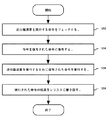
図12は、ある実施形態に従い、例示的な逆分離命令を処理するロジックのフロー図である。ブロック1202において、命令パイプラインは、逆分離演算を実行する命令をフェッチすることから始まる。実施形態によっては、命令は第1の入力オペランド、第2の入力オペランド、及びデスティネーションオペランドを受け入れる。そのような実施形態では、入力オペランドは、制御マスク及びソースレジスタを含む。ソースレジスタは、パックドバイト、ワード、ダブルワード、クワッドワードの値を格納する汎用レジスタ又はベクトルレジスタであってよい。制御マスクは、ソース汎用レジスタからのインターリーブを制御するのに用いられる汎用レジスタに提供されてよく、又はソースベクトルレジスタの各要素に提供されてもよい。1つの実施形態では、制御マスクは、ソースベクトルレジスタからのインターリーブを制御するために、ベクトルレジスタを介して提供されてよい。1つの実施形態では、デスティネーションオペランドはデスティネーションレジスタを提供し、そのレジスタは、パックドバイト、ワード、ダブルワード、又はクワッドワードの値を格納するよう構成された汎用レジスタ又はベクトルレジスタでよい。
FIG. 12 is a flow diagram of logic for processing an exemplary reverse separation instruction, according to an embodiment. At
ブロック1204において、復号ユニットが命令を復号された命令に復号する。1つの実施形態では、復号された命令は単一のオペレーションである。1つの実施形態では、復号された命令は、命令の各サブ要素を実行する1つ又は複数の論理マイクロオペレーションを含む。マイクロオペレーションは物理的に組み込まれ得る、又はマイクロコードオペレーションは、実行ユニットなどのプロセッサのコンポーネントに命令を実行する様々なオペレーションを実行させ得る。
At
ブロック1206において、プロセッサの実行ユニットが、制御マスクに基づいてソースレジスタのビットをインターリーブする逆分離(例えば、「羊と山羊」の逆)演算を実行するために復号された命令を実行する。逆分離演算を実行する例示的な論理演算が図9A〜図9Eに示されているが、実行される特定の演算は実施形態によって異なってよく、別の又は追加の論理が逆分離演算を実行するのに用いられてもよい。実行中に、プロセッサの1つ又は複数の実行ユニットが、制御マスクに基づいて、ソースレジスタ又はソースレジスタのベクトル要素の一方側又は反対側(例えば、左又は右)からソースデータを読み出す。1つの実施形態では、制御マスクビットの1は、レジスタの「右」側の値が取得されることを示し、制御マスクビットの0は、レジスタの「左」側の値が取得されることを示す。実施形態によれば、レジスタの「右」側及び「左」側はそれぞれ、レジスタの下位ビット及び上位ビットを示してよい。本明細書で説明されるように、上位ビット及び下位ビットは、データワードを構成するバイトがコンピュータメモリに格納される場合、これらのバイトを解釈するのに用いられる規則から独立した最上位ビット及び最下位ビットとして定義される。しかし、バイトオーダが実施形態及び構成によって異なり得るので、レジスタのそれぞれの側及びワードアドレス/オフセットに関連したバイトオーダが、様々な実施形態の範囲に違反することなく異なってよいことが理解されるであろう。
At
ブロック1408において、プロセッサは実行された命令の結果をプロセッサレジスタファイルに書き込む。プロセッサレジスタファイルは、様々なデータタイプを格納する1つ又は複数の物理レジスタファイルを含み、データタイプにはスカラ整数タイプ又はパックド整数データタイプが含まれる。1つの実施形態では、レジスタファイルは、命令デスティネーションオペランドによりデスティネーションレジスタとして示される汎用レジスタ又はベクトルレジスタを含む。
[例示的な命令フォーマット]
At block 1408, the processor writes the result of the executed instruction to the processor register file. The processor register file includes one or more physical register files that store various data types, and the data type includes a scalar integer type or a packed integer data type. In one embodiment, the register file includes a general purpose register or vector register indicated as a destination register by an instruction destination operand.
[Example instruction format]
本明細書で説明される命令の実施形態は、異なるフォーマットに具現化されてもよい。さらに、例示的なシステム、アーキテクチャ、及びパイプラインが以下に詳述されている。命令の実施形態は、そのようなシステム、アーキテクチャ、及びパイプライン上で実行されてよいが、詳述されたこれらのものに限定されない。 The instruction embodiments described herein may be embodied in different formats. In addition, exemplary systems, architectures, and pipelines are detailed below. Instruction embodiments may execute on such systems, architectures, and pipelines, but are not limited to those detailed.
ベクトル対応命令フォーマットは、ベクトル命令に適した命令フォーマットである(例えば、ベクトル演算に固有の特定のフィールドがある)。ベクトル演算及びスカラ演算の両方がベクトル対応命令フォーマットを通じてサポートされる実施形態が説明されるが、代替的な実施形態は、ベクトル対応命令フォーマットを通じてサポートされるベクトル演算のみを用いる。 The vector corresponding instruction format is an instruction format suitable for vector instructions (for example, there are specific fields specific to vector operations). Although embodiments are described in which both vector and scalar operations are supported through a vector-enabled instruction format, alternative embodiments use only vector operations supported through a vector-enabled instruction format.
図13A〜図13Bは、ある実施形態に従い、汎用ベクトル対応命令フォーマット及びその命令テンプレートを示すブロック図である。図13Aは、ある実施形態に従い、汎用ベクトル対応命令フォーマット及びそのクラスA命令テンプレートを示すブロック図であり、図13Bは、ある実施形態に従い、汎用ベクトル対応命令フォーマット及びそのクラスB命令テンプレートを示すブロック図である。具体的には、汎用ベクトル対応命令フォーマット1300に対して、クラスA命令テンプレート及びクラスB命令テンプレートが定義され、その両方が非メモリアクセス1305の命令テンプレート及びメモリアクセス1320の命令テンプレートを含む。ベクトル対応命令フォーマットとの関連で汎用という用語は、いかなる特定の命令セットにも関係していない命令フォーマットを意味する。
FIGS. 13A-13B are block diagrams illustrating a generic vector compatible instruction format and its instruction template according to an embodiment. FIG. 13A is a block diagram illustrating a generic vector compatible instruction format and its class A instruction template according to an embodiment, and FIG. 13B is a block diagram illustrating a generic vector compatible instruction format and its class B instruction template according to an embodiment. FIG. Specifically, a class A instruction template and a class B instruction template are defined for the general-purpose vector compatible instruction format 1300, and both include an instruction template for
実施形態が説明されるが、その中でベクトル対応命令フォーマットは以下のものをサポートする。つまり、32ビット(4バイト)又は64ビット(8バイト)データ要素幅(又はサイズ)を有する64バイトベクトルオペランド長(又はサイズ)(したがって、64バイトベクトルは、ダブルワードサイズの16個の要素、又は代わりにクワッドワードサイズの8個の要素から構成される)と、16ビット(2バイト)又は8ビット(1バイト)データ要素幅(又はサイズ)を有する64バイトベクトルオペランド長(又はサイズ)と、32ビット(4バイト)、64ビット(8バイト)、16ビット(2バイト)、又は8ビット(1バイト)データ要素幅(又はサイズ)を有する32バイトベクトルオペランド長(又はサイズ)と、32ビット(4バイト)、64ビット(8バイト)、16ビット(2バイト)、又は8ビット(1バイト)データ要素幅(又はサイズ)を有する16バイトベクトルオペランド長(又はサイズ)である。しかし、代替的な実施形態は、より大きいデータ要素幅、より小さいデータ要素幅、又は異なるデータ要素幅(例えば、128ビット(16バイト)データ要素幅)を有する、より大きいベクトルオペランドサイズ、より小さいベクトルオペランドサイズ、及び/又は異なるベクトルオペランドサイズ(例えば、256バイトベクトルオペランド)をサポートする。 Embodiments are described in which the vector-capable instruction format supports the following: That is, a 64-byte vector operand length (or size) with a 32-bit (4-byte) or 64-bit (8-byte) data element width (or size) (so a 64-byte vector is 16 elements of doubleword size, Or alternatively composed of 8 elements of quadword size) and a 64-byte vector operand length (or size) with a data element width (or size) of 16 bits (2 bytes) or 8 bits (1 byte) 32 byte vector operand length (or size) with a data element width (or size) of 32 bits (4 bytes), 64 bits (8 bytes), 16 bits (2 bytes), or 8 bits (1 byte); Bit (4 bytes), 64 bits (8 bytes), 16 bits (2 bytes), or 8 bits (1 byte) ) Is a data element width (or size) 16 bytes vector operand length with (or size). However, alternative embodiments may have larger vector operand sizes, smaller data element widths, smaller data element widths, or different data element widths (eg, 128 bit (16 byte) data element widths), smaller Support vector operand sizes and / or different vector operand sizes (eg, 256 byte vector operands).
図13AのクラスA命令テンプレートは以下のものを含む。つまり、1)非メモリアクセス1305の命令テンプレート内に示されている、非メモリアクセス・フルラウンド制御型オペレーション1310の命令テンプレート、及び非メモリアクセス・データ変換型オペレーション1315の命令テンプレート、並びに2)メモリアクセス1320の命令テンプレート内に示されている、メモリアクセス・一時的1325の命令テンプレート、及びメモリアクセス・非一時的1330の命令テンプレートである。図13BのクラスB命令テンプレートは以下のものを含む。つまり、1)非メモリアクセス1305の命令テンプレート内に示されている、非メモリアクセス・書き込みマスク制御・部分ラウンド制御型オペレーション1312の命令テンプレート、及び非メモリアクセス・書き込みマスク制御・vsize型オペレーション1317の命令テンプレート、並びに2)メモリアクセス1320命令テンプレート内に示されている、メモリアクセス・書き込みマスク制御1327の命令テンプレートである。
The class A instruction template of FIG. 13A includes: That is, 1) the instruction template of the non-memory access / full round
汎用ベクトル対応命令フォーマット1300は、図13A〜図13Bに示される順で以下に列挙する次のフィールドを含む。 The generic vector corresponding instruction format 1300 includes the following fields listed below in the order shown in FIGS. 13A-13B.
フォーマットフィールド1340:このフィールドの特定値(命令フォーマット識別子の値)は、ベクトル対応命令フォーマットを一意に特定し、したがって、命令ストリーム内のベクトル対応命令フォーマットにおける命令の出現を特定する。そのため、このフィールドは、汎用ベクトル対応命令フォーマットのみを有する命令セットには必要とされないという点で、任意なものである。 Format field 1340: The specific value of this field (the value of the instruction format identifier) uniquely identifies the vector-capable instruction format and thus identifies the occurrence of an instruction in the vector-capable instruction format in the instruction stream. Therefore, this field is optional in that it is not required for an instruction set having only a general vector compatible instruction format.
ベースオペレーションフィールド1342:このコンテンツは、異なるベースオペレーションを識別する。 Base operation field 1342: This content identifies a different base operation.
レジスタインデックスフィールド1344:このコンテンツは、ソース及びデスティネーションオペランドの位置を、それらがレジスタ内にあってもメモリ内にあっても、直接又はアドレス生成を通じて指定する。これらは、PxQ(例えば32x512、16x128、32x1024、64x1024)レジスタファイルからN個のレジスタを選択するのに十分な数のビットを含む。1つの実施形態では、Nは3つのソースレジスタ及び1つのデスティネーションレジスタまでであってよいが、代替的な実施形態はより多くの又はより少ないソースレジスタ及びデスティネーションレジスタをサポートしてもよい(例えば、2つのソース(このうち1つはデスティネーションの役割も果たす)までをサポートしてよく、3つのソース(このうち1つはデスティネーションの役割も果たす)までをサポートしてもよく、2つのソース及び1つのデスティネーションまでをサポートしてもよい)。 Register index field 1344: This content specifies the location of the source and destination operands, either in registers or in memory, either directly or through address generation. These include a sufficient number of bits to select N registers from a PxQ (eg, 32x512, 16x128, 32x1024, 64x1024) register file. In one embodiment, N may be up to three source registers and one destination register, but alternative embodiments may support more or fewer source and destination registers ( For example, up to two sources (one of which also serves as the destination) may be supported, and up to three sources (one of which also serves as the destination) may be supported. Up to one source and one destination).
修飾子フィールド1346:このコンテンツは、汎用ベクトル命令フォーマットにおいてメモリアクセスを指定する命令の出現をそうでない命令の出現と識別する。すなわち、非メモリアクセス1305の命令テンプレートとメモリアクセス1320の命令テンプレートとを識別する。メモリアクセスオペレーションは、メモリ階層を読み出す、及び/又はメモリ階層へ書き込む(場合によっては、レジスタ内の値を用いてソースアドレス及び/又はデスティネーションアドレスを指定する)が、非メモリアクセスオペレーションはこうしたことを行わない(例えば、ソース及びデスティネーションはレジスタである)。1つの実施形態では、このフィールドはまた、メモリアドレス計算を実行するための3つの異なる方法から選択するが、代替的な実施形態は、メモリアドレス計算を実行するためのより多くの方法、より少ない方法、又は異なる方法をサポートしてもよい。
Qualifier field 1346: This content identifies the occurrence of an instruction specifying memory access in the generalized vector instruction format as an occurrence of an instruction that is not. That is, the instruction template for
拡大オペレーションフィールド1350:このコンテンツは、様々な異なるオペレーションのどれがベースオペレーションに加えて実行されるかを識別する。このフィールドは、コンテキスト固有のものである。1つの実施形態では、このフィールドは、クラスフィールド1368、アルファフィールド1352、及びベータフィールド1354に分割される。拡大オペレーションフィールド1350は、共通グループのオペレーションが2つ、3つ、又は4つの命令ではなく、単一の命令で実行されることを可能にする。
Extended Operation Field 1350: This content identifies which of a variety of different operations are performed in addition to the base operation. This field is context specific. In one embodiment, this field is divided into a class field 1368, an
スケールフィールド1360:このコンテンツは、メモリアドレス生成のために(例えば、2[スケール]×[インデックス]+[ベース]を用いるアドレス生成のために)インデックスフィールドのコンテンツをスケーリングすることを可能にする。 Scale field 1360: This content allows the content of the index field to be scaled for memory address generation (eg, for address generation using 2 [scale] x [index] + [base]).
変位フィールド1362A:このコンテンツは、(例えば、2[スケール]×[インデックス]+[ベース]+[変位]を用いるアドレス生成のために)メモリアドレス生成の一部として用いられる。
変位係数フィールド1362B(なお、変位フィールド1362Aを変位係数フィールド1362Bのすぐ上に並置することで、一方又は他方が使用されていることが示される点に注意):このコンテンツは、アドレス生成の一部として用いられ、これは、メモリアクセスのサイズ(N)でスケーリングされる変位係数を指定する。ここで、Nは、(例えば、2[スケール]×[インデックス]+[ベース]+[スケーリングされた変位]を用いるアドレス生成のための)メモリアクセス内のバイト数である。冗長下位ビットは無視され、したがって、有効アドレスの計算に用いられる最終的な変位を生成するために、変位係数フィールドのコンテンツはメモリオペランドの合計サイズ(N)を乗じる。Nの値は、フルオペコードフィールド1374(本明細書に後述)及びデータ操作フィールド1354Cに基づき、プロセッサハードウェアによって実行時に決定される。変位フィールド1362A及び変位係数フィールド1362Bは、これらが非メモリアクセス1305の命令テンプレートには用いられず、及び/又は異なる実施形態では2つのうち一方のみを実装するかどちらも実装しない場合があるという点で任意である。
データ要素幅フィールド1364:このコンテンツは、(実施形態によっては全ての命令に、他の実施形態ではいくつかの命令だけに)複数のデータ要素幅のどれが用いられるべきかを識別する。このフィールドは、1つのデータ要素幅のみがサポートされる場合、及び/又は複数のデータ要素幅がオペコードの何らかの態様を用いてサポートされる場合は、必要とされないという点で任意である。 Data element width field 1364: This content identifies which of a plurality of data element widths should be used (for all instructions in some embodiments and only some instructions in other embodiments). This field is optional in that it is not required if only one data element width is supported and / or if multiple data element widths are supported using some aspect of the opcode.
書き込みマスクフィールド1370:このコンテンツは、データ要素位置に基づいて、デスティネーションベクトルオペランドのそのデータ要素位置がベースオペレーション及び拡大オペレーションの結果を反映するかどうかを制御する。クラスA命令テンプレートは、マージ処理・書き込みマスク処理をサポートし、クラスB命令テンプレートは、マージ・書き込みマスク処理、及びゼロ設定・書き込みマスク処理の両方をサポートする。マージする場合、ベクトルマスクは、(ベースオペレーション及び拡大オペレーションによって指定される)任意のオペレーションを実行中に、デスティネーションにおける任意のセットの要素が更新から保護されることを可能とし、他の1つの実施形態では、対応するマスクビットが0である場合、デスティネーションの各要素の古い値を保護する。これに対して、ゼロにセットする場合、ベクトルマスクは、デスティネーションにおける任意のセットの要素が(ベースオペレーション及び拡大オペレーションによって指定される)任意のオペレーションの実行中にゼロにセットされることを可能とし、1つの実施形態では、対応するマスクビットの値が0である場合、デスティネーションの要素は0に設定される。この機能のサブセットは、実行されているオペレーションのベクトル長(すなわち、変更される要素の長さ、つまり最初の要素から最後の要素まで)を制御する能力である。しかし、変更される要素は連続的である必要はない。したがって、書き込みマスクフィールド1370は、ロード演算、ストア演算、算術演算、論理演算などを含む一部のベクトル演算を可能にする。書き込みマスクフィールド1370のコンテンツが用いられる書き込みマスクを含む複数の書き込みマスクレジスタのうち1つを選択する(したがって、書き込みマスクフィールド1370のコンテンツが実行されるマスク処理を間接的に特定する)実施形態が説明されるが、代替的な実施形態では代わりに又は追加的に、書き込みマスクフィールド1370のコンテンツが、実行されるマスク処理を直接指定することを可能にする。
Write mask field 1370: This content controls, based on the data element position, whether that data element position of the destination vector operand reflects the result of the base operation and the expansion operation. The class A instruction template supports merge processing / write mask processing, and the class B instruction template supports both merge / write mask processing and zero setting / write mask processing. When merging, the vector mask allows any set of elements at the destination to be protected from updating while performing any operation (specified by the base and extension operations) In an embodiment, if the corresponding mask bit is 0, the old value of each element of the destination is protected. In contrast, when set to zero, the vector mask allows any set of elements in the destination to be set to zero during the execution of any operation (specified by the base and extension operations). In one embodiment, if the value of the corresponding mask bit is 0, the destination element is set to 0. A subset of this function is the ability to control the vector length of the operation being performed (ie, the length of the element being changed, ie, from the first element to the last element). However, the elements to be changed need not be continuous. Thus, the
即値フィールド1372:このコンテンツは、即値オペランドの指定を可能とする。このフィールドは、即値をサポートしない汎用ベクトル対応フォーマットの実装には存在せず、即値を用いない命令には存在しないという点で任意である。 Immediate field 1372: This content allows specification of an immediate operand. This field is optional in that it does not exist in implementations of general-purpose vector-compatible formats that do not support immediate values, and does not exist in instructions that do not use immediate values.
クラスフィールド1368:このコンテンツは、複数の異なるクラスの命令を識別する。図13A〜図13Bに関連して、このフィールドのコンテンツは、クラスA命令及びクラスB命令から選択する。図13A〜図13Bでは、角が丸い四角が、フィールド内に特定値が存在することを示すのに用いられている(例えば、図13A〜図13Bにそれぞれあるクラスフィールド1368用のクラスA 1368A、及びクラスB 1368B)。
[クラスAの命令テンプレート]
Class field 1368: This content identifies multiple different classes of instructions. In connection with FIGS. 13A-13B, the contents of this field are selected from class A and class B instructions. In FIGS. 13A-13B, squares with rounded corners are used to indicate that a particular value exists in the field (eg,
[Class A instruction template]
クラスAの非メモリアクセス1305命令テンプレートの場合、アルファフィールド1352はRSフィールド1352Aと解釈され、そのコンテンツは、異なる拡大オペレーションタイプのどれが実行されるべきかを識別し(例えば、非メモリアクセス・ラウンド型オペレーション1310及び非メモリアクセス・データ変換型オペレーション1315の命令テンプレートに対し、ラウンド1352A.1及びデータ変換1352A.2がそれぞれ指定される)、ベータフィールド1354は、指定されるタイプのオペレーションのどれが実行されるべきかを識別する。非メモリアクセス1305の命令テンプレートには、スケールフィールド1360、変位フィールド1362A、及び変位係数フィールド1362Bが存在しない。
[非メモリアクセス命令テンプレート−フルラウンド制御型オペレーション]
For class A
[Non-memory access instruction template-Full round control operation]
非メモリアクセスフルラウンド制御型オペレーション1310の命令テンプレートにおいて、ベータフィールド1354はラウンド制御フィールド1354Aと解釈され、そのコンテンツは静的なラウンド処理を提供する。説明された実施形態では、ラウンド制御フィールド1354Aは、全浮動小数点例外抑制(SAE)フィールド1356及びラウンド演算制御フィールド1358を含むが、代替的な実施形態では、これらのコンセプトを両方ともサポートしてよく、それらを同じフィールド内に符号化してよく、あるいはこれらのコンセプト/フィールドの一方又は他方のみを有してもよい(例えば、ラウンド演算制御フィールド1358のみを有してよい)。
In the instruction template for non-memory access full round
SAEフィールド1356:このコンテンツは、例外イベント報告を無効化するかどうか識別する。SAEフィールド1356のコンテンツが、抑制が可能であることを示す場合、所与の命令は、いかなる種類の浮動小数点例外フラグも報告せず、いかなる浮動小数点例外ハンドラも呼び出さない。 SAE field 1356: This content identifies whether to disable exception event reporting. If the contents of SAE field 1356 indicate that suppression is possible, the given instruction does not report any kind of floating point exception flag and does not call any floating point exception handler.
ラウンド演算制御フィールド1358:このコンテンツは、ラウンド演算のグループのどれを実行すべきかを識別する(例えば、切り上げ、切り捨て、0への丸め、及び最近接丸め)。したがって、ラウンド演算制御フィールド1358は、命令に基づいてラウンドモードの変更を可能にする。1つの実施形態では、プロセッサが、ラウンドモードを指定する制御レジスタを含み、ラウンド演算制御フィールド1350のコンテンツは、当該レジスタの値をオーバーライドする。
[非メモリアクセス命令テンプレート−データ変換型オペレーション]
Round operation control field 1358: This content identifies which group of round operations to perform (eg, round up, round down, round to zero, and nearest round). Therefore, the round calculation control field 1358 allows the round mode to be changed based on the instruction. In one embodiment, the processor includes a control register that specifies a round mode, and the contents of the round operation control field 1350 override the value of that register.
[Non-memory access instruction template-data conversion type operation]
非メモリアクセスデータ変換型オペレーション1315の命令テンプレートでは、ベータフィールド1354はデータ変換フィールド1354Bとして解釈され、そのコンテンツは、複数のデータ変換のどれが実行されるべきかを識別する(例えば、データ変換なし、スウィズル、ブロードキャスト)。
In the instruction template for non-memory access data conversion type operation 1315,
クラスAのメモリアクセス1320の命令テンプレートの場合、アルファフィールド1352はエビクションヒントフィールド1352Bと解釈され、そのコンテンツは、エビクションヒントのどれが用いられるべきかを識別する(図13Aにおいて、一時的1352B.1及び非一時的1352B.2はそれぞれ、メモリアクセス・一時的1325の命令テンプレート及びメモリアクセス・非一時的1330の命令テンプレートに指定される)。ベータフィールド1354はデータ操作フィールド1354Cと解釈され、そのコンテンツは、(プリミティブとしても知られる)複数のデータ操作オペレーションのどれが実行されるべきかを識別する(例えば、操作なし、ブロードキャスト、ソースのアップコンバージョン、デスティネーションのダウンコンバージョン)。メモリアクセス1320の命令テンプレートはスケールフィールド1360を含み、任意で変位フィールド1362A又は変位係数フィールド1362Bを含む。
For a class
ベクトルメモリ命令は、変換サポートを用いて、メモリからのベクトルロード及びメモリへのベクトルストアを実行する。通常のベクトル命令と同様に、ベクトルメモリ命令はデータ要素単位の形式でデータをメモリから転送し、データをメモリに転送する。実際に転送される要素は、書き込みマスクとして選択されるベクトルマスクのコンテンツによって指示される。
[メモリアクセス命令テンプレート−一時的]
Vector memory instructions use translation support to perform a vector load from memory and a vector store to memory. Similar to a normal vector instruction, a vector memory instruction transfers data from the memory in a data element unit format, and transfers the data to the memory. The actual transfer element is indicated by the contents of the vector mask selected as the write mask.
[Memory Access Instruction Template-Temporary]
一時的データは、すぐに再使用されてキャッシュによる利益を享受するのに十分である可能性の高いデータである。しかし、これはヒントであり、異なるプロセッサが異なる方法でヒントを実行してよく、その方法には、ヒントを完全に無視することも含まれる。
[メモリアクセス命令テンプレート−非一時的]
Temporary data is data that is likely to be reused immediately and enjoy the benefits of cash. However, this is a hint, and different processors may perform the hint in different ways, including completely ignoring the hint.
[Memory access instruction template-non-temporary]
非一時的データは、すぐに再使用されてレベル1キャッシュにキャッシュすることから利益を享受するのに十分である可能性が低いデータであり、エビクションが優先されなければならない。しかし、これはヒントであり、異なるプロセッサが異なる方法でヒントを実行してよく、その方法には、ヒントを完全に無視することも含まれる。
[クラスBの命令テンプレート]
Non-temporary data is data that is unlikely to be sufficient to benefit from being immediately reused and cached in a
[Class B instruction template]
クラスBの命令テンプレートの場合には、アルファフィールド1352は書き込みマスク制御(Z)フィールド1352Cと解釈され、そのコンテンツは、書き込みマスクフィールド1370によって制御される書き込みマスク処理がマージ処理であるべきか、ゼロ設定処理であるべきかを識別する。
For Class B instruction templates, the
クラスBの非メモリアクセス1305の命令テンプレートの場合、ベータフィールド1354の一部はRLフィールド1357Aと解釈され、そのコンテンツは、異なる拡大オペレーションタイプのどれが実行されるべきかを識別し(例えば、非メモリアクセス・書き込みマスク制御・部分ラウンド制御型オペレーション1312の命令テンプレート、及び非メモリアクセス・書き込みマスク制御・VSIZE型オペレーション1317の命令テンプレートに対し、ラウンド1357A.1及びベクトル長(VSIZE)1357A.2がそれぞれ指定される)、ベータフィールド1354の残りは、指定されるタイプのオペレーションのどれが実行されるべきかを識別する。非メモリアクセス1305の命令テンプレートには、スケールフィールド1360、変位フィールド1362A、及び変位係数フィールド1362Bが存在しない。
For class B
非メモリアクセス・書き込みマスク制御・部分ラウンド制御型オペレーション1312の命令テンプレートでは、ベータフィールド1354の残りのものはラウンド演算フィールド1359Aと解釈され、例外イベント報告は無効にされる(所与の命令は、いかなる種類の浮動小数点例外フラグも報告せず、いかなる浮動小数点例外ハンドラも呼び出さない)。
In the instruction template for non-memory access / write mask control / partial round control type operation 1312, the rest of the
ラウンド演算制御フィールド1359A:ラウンド演算制御フィールド1358と全く同じように、このコンテンツは、ラウンド演算のグループのどれを実行すべきかを識別する(例えば、切り上げ、切り捨て、0への丸め、及び最近接丸め)。したがって、ラウンド演算制御フィールド1359Aは、命令に基づいてラウンドモードの変更を可能にする。1つの実施形態では、プロセッサが、ラウンドモードを指定する制御レジスタを含み、ラウンド演算制御フィールド1350のコンテンツは、当該レジスタの値をオーバーライドする。 Round Arithmetic Control Field 1359A: Just like the Round Arithmetic Control Field 1358, this content identifies which group of round arithmetic to perform (eg, round up, round down, round to zero, and nearest round). ). Accordingly, the round calculation control field 1359A allows the round mode to be changed based on the instruction. In one embodiment, the processor includes a control register that specifies a round mode, and the contents of the round operation control field 1350 override the value of that register.
非メモリアクセス・書き込みマスク制御・VSIZE型オペレーション1317の命令テンプレートでは、ベータフィールド1354の残りのものはベクトル長フィールド1359Bと解釈され、そのコンテンツは、複数のデータベクトル長のどれが実行されるべきかを識別する(例えば、128バイト、256バイト、又は512バイト)。
In the instruction template for non-memory access, write mask control, and VSIZE type operation 1317, the rest of the
クラスBのメモリアクセス1320の命令テンプレートの場合には、ベータフィールド1354の一部はブロードキャストフィールド1357Bと解釈され、そのコンテンツは、ブロードキャスト型のデータ操作オペレーションが実行されるべきかどうかを識別し、ベータフィールド1354の残りはベクトル長フィールド1359Bと解釈される。メモリアクセス1320の命令テンプレートはスケールフィールド1360を含み、任意で変位フィールド1362A又は変位係数フィールド1362Bを含む。
In the case of a class
汎用ベクトル対応命令フォーマット1300に関して、フォーマットフィールド1340、ベースオペレーションフィールド1342、及びデータ要素幅フィールド1364を含むフルオペコードフィールド1374が示されている。フルオペコードフィールド1374がこれらのフィールド全てを含む1つの実施形態が示されているが、これらを全てサポートしない実施形態では、フルオペコードフィールド1374は、これら全てのフィールドより少ないフィールドを含む。フルオペコードフィールド1374は、オペレーションコード(オペコード)を提供する。
A full opcode field 1374 that includes a
拡大オペレーションフィールド1350、データ要素幅フィールド1364、及び書き込みマスクフィールド1370は、これらの機能が汎用ベクトル対応命令フォーマットの命令に基づいて指定されることを可能にする。
The extended operation field 1350, the data
書き込みマスクフィールドとデータ要素幅フィールドの組み合わせは、それらが異なるデータ要素幅に基づいてマスクが適用されることを可能にするという点で、型付き命令を形成する。 The combination of the write mask field and the data element width field forms a typed instruction in that they allow the mask to be applied based on different data element widths.
クラスA及びクラスB内で見られる様々な命令テンプレートは、異なる状況において有益である。実施形態によっては、異なるプロセッサ又はプロセッサ内の異なるコアが、クラスAのみ、クラスBのみ、又は両方のクラスをサポートしてよい。例えば、汎用計算を対象とした高性能汎用アウトオブオーダコアは、クラスBのみをサポートしてよく、グラフィックス及び/又は科学的(スループット)計算を主に対象としたコアは、クラスAのみをサポートしてよく、両方を対象としたコアは、両方をサポートしてよい(もちろん、コアは、両方のクラスのテンプレート及び命令の何らかの組み合わせを有するが、両方のクラスの全てのテンプレート及び命令が本発明の範囲内にあるわけではない)。また、単一のプロセッサは複数のコアを含んでよく、その全てが同じクラスをサポートし、又はその異なるコアが異なるクラスをサポートする。例えば、別個のグラフィックス及び汎用コアを有するプロセッサにおいて、グラフィックス及び/又は科学計算を主に対象とする複数のグラフィックスコアのうち1つがクラスAのみをサポートしてよく、複数の汎用コアのうち1つ又は複数が、クラスBのみをサポートする汎用計算を対象としたアウトオブオーダ実行及びレジスタリネーミングを有する高性能汎用コアであってもよい。別個のグラフィックスコアを持たない別のプロセッサは、クラスA及びクラスBの両方をサポートするもう1つの汎用インオーダ又はアウトオブオーダコアを含んでよい。もちろん、一方のクラスの特徴はまた、異なる実施形態において他方のクラスに実装されてよい。高水準言語で書かれたプログラムは、以下の形式を含む様々な異なる実行可能形式に変換される(例えば、ジャスト・イン・タイム方式でコンパイルされる、又は静的にコンパイルされる)であろう。例えば、1)実行用ターゲットプロセッサによってサポートされるクラスの命令のみを有する形式、あるいは2)全クラスの命令の異なる組み合わせを用いて書かれた代替ルーチンを有し、プロセッサによってサポートされる命令に基づいて、実行するルーチンを選択する制御フローコードを有する形式であって、当該プロセッサが当該コードを現時点で実行している、形式である。
[例示的な特定ベクトル対応命令フォーマット]
The various instruction templates found within class A and class B are useful in different situations. In some embodiments, different processors or different cores within a processor may support class A only, class B only, or both classes. For example, a high-performance general-purpose out-of-order core targeted at general-purpose computations may support only class B, and a core primarily targeted at graphics and / or scientific (throughput) computations may only support class A. A core that supports both may support both (of course, the core has some combination of templates and instructions for both classes, but all templates and instructions for both classes Not within the scope of the invention). A single processor may also include multiple cores, all of which support the same class, or different cores that support different classes. For example, in a processor having separate graphics and general purpose cores, one of a plurality of graphics scores mainly directed to graphics and / or scientific computation may support only class A, One or more may be high performance general purpose cores with out-of-order execution and register renaming for general purpose computations that support only class B. Another processor that does not have a separate graphic score may include another general-purpose in-order or out-of-order core that supports both class A and class B. Of course, features of one class may also be implemented in the other class in different embodiments. A program written in a high-level language will be translated into a variety of different executable formats, including the following formats (eg compiled just-in-time or statically compiled) . For example, 1) a format having only instructions of a class supported by the target processor for execution, or 2) having an alternative routine written using a different combination of instructions of all classes and based on instructions supported by the processor Thus, it is a format having a control flow code for selecting a routine to be executed, and the processor is currently executing the code.
[Example of instruction format for specific vector]
図14A〜図14Dは、ある実施形態に従って例示的な特定ベクトル対応命令フォーマットを示すブロック図である。図14Aは、特定ベクトル対応命令フォーマット1400を示し、これは位置、サイズ、解釈、及びフィールドの順序、並びにこれらのフィールドのいくつかに対する値を指定するという点で特定のものである。特定ベクトル対応命令フォーマット1400は、x86命令セットを拡張するのに用いられてよく、したがって、フィールドのいくつかは、既存のx86命令セット及びその拡張版(例えば、AVX)に用いられるものと同様又は同じである。このフォーマットは、拡張された既存のx86命令セットのプリフィックス符号化フィールド、リアルオペコードバイトフィールド、MOD R/Mフィールド、SIBフィールド、変位フィールド、及び即値フィールドと一致した状態のままである。図14Aのフィールドがマッピングされる図13A〜図13Bのフィールドが示されている。 14A-14D are block diagrams illustrating exemplary specific vector-capable instruction formats in accordance with some embodiments. FIG. 14A shows a specific vector support instruction format 1400 that is specific in that it specifies the position, size, interpretation, and order of fields, and values for some of these fields. The specific vector support instruction format 1400 may be used to extend the x86 instruction set, and therefore some of the fields are similar to those used in the existing x86 instruction set and its extensions (eg, AVX) or The same. This format remains consistent with the existing extended x86 instruction set prefix encoded field, real opcode byte field, MOD R / M field, SIB field, displacement field, and immediate field. The fields of FIGS. 13A-13B to which the fields of FIG. 14A are mapped are shown.
実施形態は、例示を目的として汎用ベクトル対応命令フォーマット1300との関連で特定ベクトル対応命令フォーマット1400に関連して説明されるが、本発明は、特許請求される場合を除いて、特定ベクトル対応命令フォーマット1400に限定されないことが理解されるべきである。例えば、汎用ベクトル対応命令フォーマット1300では、様々なフィールドについて様々な可能なサイズを検討するが、特定ベクトル対応命令フォーマット1400は、特定のサイズのフィールドを有するものとして示されている。具体例として、データ要素幅フィールド1364が、特定ベクトル対応命令フォーマット1400内の1ビットフィールドとして示されているが、本発明はそのように限定されてはいない(すなわち、汎用ベクトル対応命令フォーマット1300では、他のサイズのデータ要素幅フィールド1364を検討する)。
Although the embodiments are described in connection with a specific vector compatible instruction format 1400 in the context of a generic vector compatible instruction format 1300 for purposes of illustration, the present invention is not specific to the specific vector compatible instruction except where claimed. It should be understood that the format is not limited to 1400. For example, the generic vector support instruction format 1300 considers various possible sizes for various fields, while the specific vector support instruction format 1400 is shown as having a field of a specific size. As a specific example, the data
汎用ベクトル対応命令フォーマット1300は、図14Aに示される順で以下に列挙される次のフィールドを含む。 The generic vector capable instruction format 1300 includes the following fields listed below in the order shown in FIG. 14A.
EVEXプリフィックス(バイト0−3)1402:4バイト形式で符号化される。 EVEX prefix (bytes 0-3) 1402: encoded in a 4-byte format.
フォーマットフィールド1340(EVEXバイト0、ビット[7:0]:1番目のバイト(EVEXバイト0)はフォーマットフィールド1340であり、ここには0x62(本発明の1つの実施形態において、ベクトル対応命令フォーマットを識別するのに用いられる固有値)が入っている。
Format field 1340 (
2〜4番目のバイト(EVEXバイト1−3)は、特定の機能を提供する複数のビットフィールドを含む。 The second to fourth bytes (EVEX bytes 1-3) include a plurality of bit fields that provide a specific function.
REXフィールド1405(EVEXバイト1、ビット[7−5]):EVEX.Rビットフィールド(EVEXバイト1、ビット[7]−R)、EVEX.Xビットフィールド(EVEXバイト1、ビット[6]−X)、及びEVEX.Bビットフィールド(EVEXバイト1、ビット[5]−B)から構成される。EVEX.Rビットフィールド、EVEX.Xビットフィールド、及びEVEX.Bビットフィールドは、対応するVEXビットフィールドと同じ機能を提供し、1の補数形式を用いて符号化される。すなわち、ZMM0は1111Bとして符号化され、ZMM15は0000Bとして符号化される。当技術分野において知られているように、命令の他のフィールドは、レジスタインデックスの下位3ビット(rrr、xxx、及びbbb)を符号化し、EVEX.R、EVEX.X、及びEVEX.Bを加えることで、Rrrr、Xxxx、Bbbbが形成され得る。
REX field 1405 (
REX´フィールド1310:これはREX´フィールド1310の1番目の部分であり、拡張された32個のレジスタセットの上位16又は下位16を符号化するのに用いられるEVEX.R´ビットフィールド(EVEXバイト1、ビット[4]−R´)である。1つの実施形態では、このビットは、以下に示されるように他のビットと共にビット反転フォーマットで格納され、(周知のx86の32ビットモードにおいて)BOUND命令と識別する。BOUND命令のリアルオペコードバイトは62であるが、(後述の)MOD R/MフィールドにおいてMODフィールドの値11を受け付けない。代替的な実施形態は、このビット及び他の以下に示されるビットを反転フォーマットで格納しない。1の値が、下位16個のレジスタを符号化するのに用いられる。換言すると、EVEX.R´、EVEX.R、及び他のフィールドの他のRRRを組み合わせことで、R´Rrrrが形成される。
REX 'field 1310: This is the first part of the REX'
オペコードマップフィールド1415(EVEXバイト1、ビット[3:0]−mmmm):このコンテンツは、暗黙の先頭オペコードバイト(0F、0F38、又は0F3)を符号化する。
Opcode map field 1415 (
データ要素幅フィールド1364(EVEXバイト2、ビット[7]−W):EVEX.Wという表記によって表される。EVEX.Wは、データタイプ(32ビットデータ要素又は64ビットデータ要素)の粒度(サイズ)を定義するのに用いられる。
Data element width field 1364 (
EVEX.vvvv1420(EVEXバイト2、ビット[6:3]−vvvv):EVEX.vvvvの役割は以下のことを含み得る。1)EVEX.vvvvは、第1のソースレジスタオペランドを符号化し、反転(1の補数)形式で指定され、2又はそれより多くのソースオペランドを有する命令に有効である。2)EVEX.vvvvは、デスティネーションレジスタオペランドを符号化し、特定のベクトルシフトについて1の補数形式で指定される。又は、3)EVEX.vvvvはいかなるオペランドも符号化せず、フィールドは保留され1111bを含むことになる。したがって、EVEX.vvvvフィールド1420は、反転(1の補数)形式で格納される第1のソースレジスタ指定子の下位ビット4つを符号化する。命令に応じて、追加の異なるEVEXビットフィールドが、指定子サイズを32個のレジスタに拡張するのに用いられる。
EVEX. vvvv1420 (
EVEX.Uクラスフィールド1368(EVEXバイト2、ビット[2]−U):EVEX.U=0の場合にクラスA又はEVEX.U0を示し、EVEX.U=1の場合にクラスB又はEVEX.U1を示す。
EVEX. U class field 1368 (
プリフィックス符号化フィールド1425(EVEXバイト2、ビット[1:0]−pp):ベースオペレーションフィールドに追加のビットを提供する。EVEXプリフィックスフォーマットのレガシSSE命令にサポートを提供することに加え、SIMDプリフィックスを圧縮するという利点も有する(SIMDプリフィックスを示すのに1バイトを必要とするのではなく、EVEXプリフィックスは2ビットしか必要としない)。1つの実施形態では、レガシフォーマット及びEVEXプリフィックスフォーマットの両方でSIMDプリフィックス(66H、F2H、F3H)を用いるレガシSSE命令をサポートすべく、これらのレガシSIMDプリフィックスはSIMDプリフィックス符号化フィールドに符号化され、実行時には、デコーダのPLAに提供される前にレガシSIMDプリフィックスに拡張される(そのため、PLAは、これらのレガシ命令のレガシフォーマットとEVEXフォーマットとの両方を変更せずに実行し得る)。より新たな命令がEVEXプリフィックス符号化フィールドのコンテンツをオペコード拡張として直接用いる場合があるが、特定の実施形態は一貫性のために同様の形式で拡張しても、これらのレガシSIMDプリフィックスによって指定される異なる目的を可能とする。代替的な実施形態は、2ビットSIMDプリフィックス符号化をサポートするようにPLAを再設計してよく、したがって拡張を必要としない。
Prefix encoding field 1425 (
アルファフィールド1352(EVEXバイト3、ビット[7]−EH、EVEX.EH、EVEX.rs、EVEX.RL、EVEX.write mask control、及びEVEX.Nとしても知られ、αでも示される):前述したように、このフィールドはコンテキスト固有である。
Alphafield 1352 (
ベータフィールド1354(EVEXバイト3、ビット[6:4]−SSS、EVEX.s2−0、EVEX.r2−0、EVEX.rr1、EVEX.LL0、EVEX.LLBとしても知られ、βββでも示される):前述したように、このフィールドはコンテキスト固有である。
Beta field 1354 (
REX´フィールド1310:これは、REX´フィールドの残りであり、拡張された32個のレジスタセットの上位16又は下位16を符号化するのに用いられ得るEVEX.V´ビットフィールド(EVEXバイト3、ビット[3]−V´)である。このビットは、ビット反転フォーマットで格納される。1の値が、下位16個のレジスタを符号化するのに用いられる。換言すると、V´VVVVは、EVEX.V´、EVEX.vvvvを組み合わせることで形成される。
REX 'field 1310: This is the rest of the REX' field and is the EVEX..16 that can be used to encode the upper 16 or lower 16 of the extended 32 register set. V ′ bit field (
書き込みマスクフィールド1370(EVEXバイト3、ビット[2:0]−kkk):このコンテンツは、前述したように、書き込みマスクレジスタにおいてレジスタのインデックスを指定する。1つの実施形態では、特定値EVEX.kkk=000は、いかなる書き込みマスクも特定の命令に用いられないことを示唆する特別な挙動を有する(これは、全て1に物理的に組み込まれた書き込みマスクの使用、又はマスキングハードウェアをバイパスするハードウェアの使用を含む様々な方法で実装され得る)。
Write mask field 1370 (
リアルオペコードフィールド1430(バイト4)はまた、オペコードバイトとしても知られている。そのオペコードの一部はこのフィールドに指定されている。 The real opcode field 1430 (byte 4) is also known as the opcode byte. Part of the opcode is specified in this field.
MOD R/Mフィールド1440(バイト5)は、MODフィールド1442、Regフィールド1444、及びR/Mフィールド1446を含む。前述したように、MODフィールド1442のコンテンツは、メモリアクセスオペレーションと非メモリアクセスオペレーションとを識別する。Regフィールド1444の役割は、デスティネーションレジスタオペランド又はソースレジスタオペランドを符号化すること、あるいはオペコード拡張として扱われ、いかなる命令オペランドを符号化するのにも用いられないこと、という2つの状況に要約され得る。R/Mフィールド1446の役割は、メモリアドレスを参照する命令オペランドを符号化すること、あるいはデスティネーションレジスタオペランド又はソースレジスタオペランドを符号化することを含んでよい。
The MOD R / M field 1440 (byte 5) includes a
スケール・インデックス・ベース(SIB)バイト(バイト6):前述したように、スケールフィールド1350のコンテンツは、メモリアドレス生成に用いられる。SIB.xxx1454及びSIB.bbb1456:これらのフィールドのコンテンツは、レジスタインデックスXxxx及びBbbbに関して前述されている。 Scale Index Base (SIB) byte (byte 6): As described above, the contents of the scale field 1350 are used for memory address generation. SIB. xxx1454 and SIB. bbb1456: The contents of these fields are described above with respect to register indices Xxxxx and Bbbb.
変位フィールド1362A(バイト7−10):MODフィールド1442に10が入っている場合、バイト7−10は変位フィールド1362Aであり、これは、レガシ32ビット変位(disp32)と同じように機能し、バイト粒度で機能する。
変位係数フィールド1362B(バイト7):MODフィールド1442に01が入っている場合、バイト7は変位係数フィールド1362Bである。このフィールドの位置は、バイト粒度で機能するレガシx86命令セットの8ビット変位(disp8)のものと同じである。disp8は符号拡張されているので、−128と127バイトとの間のオフセットをアドレス指定できるだけであり、64バイトキャッシュラインに関しては、disp8は本当に有用な4つの値−128、−64、0及び64にだけ設定され得る8ビットを用いる。より広い範囲が必要となることが多いのでdisp32が用いられるが、disp32は4バイトを必要とする。disp8及びdisp32と対照的に、変位係数フィールド1362Bはdisp8を再解釈したものであり、変位係数フィールド1362Bを用いる場合、実際の変位は、メモリオペランドアクセスのサイズ(N)を乗じた変位係数フィールドのコンテンツによって決定される。このタイプの変位は、disp8×Nと呼ばれる。これにより、平均命令長(変位のために用いられる単一のバイトであるが、はるかに広い範囲を有する)が減少する。そのような圧縮された変位は、有効変位がメモリアクセスの粒度の倍数であるという前提に基づいており、したがって、アドレスオフセットの冗長下位ビットは、符号化される必要がない。換言すると、変位係数フィールド1362Bは、レガシx86命令セットの8ビット変位を代用する。したがって、変位係数フィールド1362Bは、disp8がdisp8×Nにオーバーロードされることを唯一の例外として、x86命令セットの8ビット変位と同じように符号化される(そのため、ModRM/SIB符号化ルールに変更はない)。換言すると、符号化ルール又は符号化長に変更はなく、ハードウェアによる変位値の解釈にだけ変更がある(これにより、バイト単位のアドレスオフセットを取得するために、メモリオペランドのサイズによって変位をスケーリングすることが必要となる)。
即値フィールド1372は、前述したように動作する。
[フルオペコードフィールド]
The
[Full opcode field]
図14Bは、1つの実施形態に従って、フルオペコードフィールド1374を構成する特定ベクトル対応命令フォーマット1400のフィールドを示すブロック図である。具体的には、フルオペコードフィールド1374は、フォーマットフィールド1340、ベースオペレーションフィールド1342、及びデータ要素幅(W)フィールド1364を含む。ベースオペレーションフィールド1342は、プリフィックス符号化フィールド1425、オペコードマップフィールド1415、及びリアルオペコードフィールド1430を含む。
[レジスタインデックスフィールド]
FIG. 14B is a block diagram that illustrates the fields of the specific vector support instruction format 1400 that make up the full opcode field 1374 according to one embodiment. Specifically, full opcode field 1374 includes a
[Register index field]
図14Cは、1つの実施形態に従って、レジスタインデックスフィールド1344を構成する特定ベクトル対応命令フォーマット1400のフィールドを示すブロック図である。具体的には、レジスタインデックスフィールド1344は、REXフィールド1405、REX´フィールド1410、MODR/M.regフィールド1444、MODR/M.r/mフィールド1446、VVVVフィールド1420、xxxフィールド1454、及びbbbフィールド1456を含む。
[拡大オペレーションフィールド]
FIG. 14C is a block diagram illustrating the fields of the specific vector support instruction format 1400 that make up the
[Expanded operation field]
図14Dは、1つの実施形態に従って、拡大オペレーションフィールド1350を構成する特定ベクトル対応命令フォーマット1400のフィールドを示すブロック図である。クラス(U)フィールド1368に0が入っている場合、これはEVEX.U0(クラスA1368A)を意味し、1が入っている場合には、EVEX.U1(クラスB1368B)を意味する。U=0、且つMODフィールド1442に11が入っている場合(非メモリアクセスオペレーションを意味する)、アルファフィールド1352(EVEXバイト3、ビット[7]−EH)はrsフィールド1352Aと解釈される。rsフィールド1352Aに1が入っている場合(ラウンド1352A.1)、ベータフィールド1354(EVEXバイト3、ビット[6:4]−SSS)はラウンド制御フィールド1354Aと解釈される。ラウンド制御フィールド1354Aは、1ビットのSAEフィールド1356及び2ビットのラウンド演算フィールド1358を含む。rsフィールド1352Aに0が入っている場合(データ変換1352A.2)、ベータフィールド1354(EVEXバイト3、ビット[6:4]−SSS)は3ビットのデータ変換フィールド1354Bと解釈される。U=0、且つMODフィールド1442に00、01、又は10が入っている場合(メモリアクセスオペレーションを意味する)、アルファフィールド1352(EVEXバイト3、ビット[7]−EH)はエビクションヒント(EH)フィールド1352Bと解釈され、ベータフィールド1354(EVEXバイト3、ビット[6:4]−SSS)は3ビットのデータ操作フィールド1354Cと解釈される。
FIG. 14D is a block diagram illustrating the fields of the specific vector support instruction format 1400 that make up the expanded operation field 1350, according to one embodiment. If the class (U) field 1368 contains 0, this is EVEX. U0 (class A1368A), and when 1 is entered, EVEX. It means U1 (
U=1の場合、アルファフィールド1352(EVEXバイト3、ビット[7]−EH)は書き込みマスク制御(Z)フィールド1352Cと解釈される。U=1、且つMODフィールド1442に11が入っている場合(非メモリアクセスオペレーションを意味する)、ベータフィールド1354(EVEXバイト3、ビット[4]−S0)の一部はRLフィールド1357Aと解釈され、1(ラウンド1357A.1)が入っている場合には、ベータフィールド1354(EVEXバイト3、ビット[6−5]−S2−1)の残りはラウンド演算フィールド1359Aと解釈される。RLフィールド1357Aに0(VSIZE1357.A2)が入っている場合、ベータフィールド1354(EVEXバイト3、ビット[6−5]−S2−1)の残りはベクトル長フィールド1359B(EVEXバイト3、ビット[6−5]−L1−0)と解釈される。U=1、且つMODフィールド1442に00、01、又は10が入っている場合(メモリアクセスオペレーションを意味する)、ベータフィールド1354(EVEXバイト3、ビット[6:4]−SSS)は、ベクトル長フィールド1359B(EVEXバイト3、ビット[6−5]−L1−0)及びブロードキャストフィールド1357B(EVEXバイト3、ビット[4]−B)と解釈される。
[例示的なレジスタアーキテクチャ]
When U = 1, the alpha field 1352 (
[Example Register Architecture]
図15は、1つの実施形態によるレジスタアーキテクチャ1500のブロック図である。示される実施形態には、512ビット幅の32個のベクトルレジスタ1510があり、これらのレジスタは、zmm0〜zmm31と参照符号が付けられている。下位16個のzmmレジスタの下位256ビットは、レジスタymm0〜15にオーバーレイされる。下位16個のzmmレジスタの下位128ビット(ymmレジスタの下位128ビット)は、レジスタxmm0〜15にオーバーレイされる。特定ベクトル対応命令フォーマット1400は、以下の表3に示されるように、これらのオーバーレイされたレジスタを処理する。
換言すると、ベクトル長フィールド1359Bは、最大長さと1つ又は複数の他のより短い長さとの間から選択し、このようなより短い長さはそれぞれ、前述の長さの半分の長さであり、ベクトル長フィールド1359Bを用いない命令テンプレートは、最大ベクトル長を処理する。さらに1つの実施形態では、特定ベクトル対応命令フォーマット1400のクラスB命令テンプレートは、パックド又はスカラ単精度/倍精度浮動小数点データ、及びパックド又はスカラ整数データを処理する。スカラ演算は、zmm/ymm/xmmレジスタ内の最下位データ要素位置において実行される演算であり、上位のデータ要素位置は、実施形態に応じて、命令の前と同じ状態のままにされるか又はゼロにセットされる。
In other words, the
書き込みマスクレジスタ1515:示される実施形態には、8個の書き込みマスクレジスタ(k0〜k7)があり、それぞれのサイズは64ビットである。代替的な実施形態において、書き込みマスクレジスタ1515のサイズは16ビットである。前述したように、1つの実施形態では、ベクトルマスクレジスタk0は書き込みマスクとして用いられることができず、k0を標準的に示すであろう符号化が書き込みマスクに用いられる場合、これは、物理的に組み込まれた0xFFFFという書き込みマスクを選択し、当該命令用の書き込みマスクを効果的に無効にする。 Write mask register 1515: In the embodiment shown, there are eight write mask registers (k0-k7), each of which is 64 bits in size. In an alternative embodiment, the size of the write mask register 1515 is 16 bits. As described above, in one embodiment, the vector mask register k0 cannot be used as a write mask, and if an encoding that would normally indicate k0 is used for the write mask, Is selected, and the write mask for the instruction is effectively invalidated.
汎用レジスタ1525:示される実施形態には、メモリオペランドをアドレス指定する既存のx86アドレッシングモードと共に用いられる16個の64ビット汎用レジスタが存在する。これらのレジスタには、RAX、RBX、RCX、RDX、RBP、RSI、RDI、RSP、及びR8〜R15という名称で参照符号が付けられている。 General purpose registers 1525: In the embodiment shown, there are 16 64-bit general purpose registers used with the existing x86 addressing mode to address memory operands. These registers are labeled with the names RAX, RBX, RCX, RDX, RBP, RSI, RDI, RSP, and R8-R15.
MMXパックド整数フラットレジスタファイル1550がエイリアスされるスカラ浮動小数点スタックレジスタファイル(x87スタック)1545:示される実施形態において、x87スタックは、x87命令セット拡張を用いて32/64/80ビット浮動小数点データに対してスカラ浮動小数点演算を実行するのに用いられる8要素スタックである。一方、MMXレジスタは、64ビットパックド整数データに対して演算を実行するのに用いられ、さらにMMXとXMMレジスタとの間で実行される一部の演算用にオペランドを保持するのに用いられる。 Scalar floating point stack register file (x87 stack) 1545 to which MMX packed integer flat register file 1550 is aliased: In the illustrated embodiment, the x87 stack is converted to 32/64/80 bit floating point data using the x87 instruction set extension. It is an 8-element stack used to perform scalar floating point operations on it. The MMX register, on the other hand, is used to perform operations on 64-bit packed integer data and is also used to hold operands for some operations performed between the MMX and XMM registers.
代替的な実施形態は、より広いレジスタを用いても、又はより狭いレジスタを用いてもよい。さらに、代替的な実施形態は、より多くのレジスタファイル、より少ないレジスタファイル、又は異なるレジスタファイル及びレジスタを用いてもよい。 Alternative embodiments may use wider registers or narrower registers. Further, alternative embodiments may use more register files, fewer register files, or different register files and registers.
本明細書で説明されるのは、システムに動作を実行させるためにソフトウェア、ファームウェア、ハードウェア、又はこれらの組み合わせをシステム上にインストールすることにより、特定のオペレーション又は動作を実行するよう構成され得る1つ又は複数のコンピュータのシステムである。さらに、1つ又は複数のコンピュータプログラムは、処理装置により実行又は利用された場合に、本明細書で説明された動作を装置に実行させる命令又はハードウェアロジックを含めることにより、特定のオペレーション又は動作を実行するよう構成され得る。1つの実施形態では、処理装置は、第1の命令を第1のオペランド及び第2オペランドを含んだ第1の復号された命令に復号する復号ロジックと、逆分離演算を実行するために第1の復号された命令を実行する実行ユニットとを含む。 Described herein may be configured to perform a particular operation or operation by installing software, firmware, hardware, or a combination of these on the system to cause the system to perform the operation. A system of one or more computers. In addition, one or more computer programs may contain specific operations or operations by including instructions or hardware logic that, when executed or utilized by a processing device, cause the device to perform the operations described herein. May be configured to perform. In one embodiment, the processing device includes decoding logic that decodes a first instruction into a first decoded instruction that includes a first operand and a second operand, and a first to perform an inverse separation operation. Execution unit for executing the decoded instructions.
逆分離命令は、第2のオペランドにより指定されるソースレジスタの両領域のビットを、第1のオペランドにより示される制御マスクに基づいてインターリーブする。1つの実施形態では、第2のオペランドは、それがアーキテクチャレジスタを示す限り、ソースレジスタを指定し、これは、ソースデータ又はソースデータ要素を格納する汎用レジスタ又はベクトルレジスタであってよい。第1のオペランドは、それがアーキテクチャレジスタをリストに加える限り、制御マスクを示し、又は1つの実施形態では即値オペランドとして制御マスク値を直接示してよく、又は制御マスクを含んだメモリアドレスを含んでもよい。他の実施形態は、対応するコンピュータシステム、装置、及び1つ又は複数のコンピュータストレージデバイスに記録されるコンピュータプログラムを含み、それぞれは、本明細書で指定された動作を実行するよう構成される。 The reverse separation instruction interleaves the bits of both areas of the source register specified by the second operand based on the control mask indicated by the first operand. In one embodiment, the second operand designates a source register as long as it indicates an architecture register, which may be a general purpose register or vector register that stores source data or source data elements. The first operand indicates the control mask as long as it adds an architecture register to the list, or in one embodiment may indicate the control mask value directly as an immediate operand, or may include a memory address that includes the control mask. Good. Other embodiments include corresponding computer systems, apparatus, and computer programs recorded on one or more computer storage devices, each configured to perform the operations specified herein.
例えば、1つの実施形態では、処理装置は第1の命令をフェッチする命令フェッチユニットをさらに含み、この命令は単一の機械レベル命令である。1つの実施形態では、処理装置は、本明細書で説明される逆分離演算の結果をデスティネーションオペランドにより指定される位置にコミットするレジスタファイルをさらに含み、これは汎用レジスタでもベクトルレジスタでもよい。レジスタファイルユニットは、第1のソースオペランド値を格納する第1のレジスタと、第2のソースオペランド値を格納する第2のレジスタと、前述の分離演算の結果の少なくとも1つのデータ要素を格納する第3のレジスタとを含む物理レジスタのセットを格納するよう構成され得る。 For example, in one embodiment, the processing device further includes an instruction fetch unit that fetches a first instruction, which is a single machine level instruction. In one embodiment, the processing device further includes a register file that commits the result of the inverse separation operation described herein to the location specified by the destination operand, which may be a general purpose register or a vector register. The register file unit stores a first register for storing a first source operand value, a second register for storing a second source operand value, and at least one data element resulting from the above-described separation operation. It may be configured to store a set of physical registers including a third register.
1つの実施形態では、第1のレジスタは制御マスクを格納し、制御マスクは複数のビットを含み、制御マスクの各ビットは、値を読み出すためのソースレジスタ内のビット位置を示す。1つの実施形態では、制御マスクビットの1は、第2のレジスタの第1の領域の値が取得されることを示し、制御マスクビットの0は、第2のレジスタの第2の領域の値が取得されることを示す。 In one embodiment, the first register stores a control mask, the control mask includes a plurality of bits, and each bit of the control mask indicates a bit position in the source register for reading a value. In one embodiment, a control mask bit of 1 indicates that the value of the first region of the second register is obtained, and a control mask bit of 0 indicates the value of the second region of the second register. Indicates that is acquired.
1つの実施形態では、第2のレジスタの第1の領域は、当該レジスタの下位のバイトオーダビットを含み、第2のレジスタの第2の領域は、当該レジスタの上位のバイトオーダビットを含む。1つの実施形態では、第1の領域のより下位のバイトオーダのビットは、レジスタの「右」側に分類され、第2の領域の上位のバイトオーダビットはレジスタの「左」側に分類される。しかし、逆分離演算は、レジスタに関連したバイトオーダ又はアドレス規則に関して限定することなく、レジスタの両側、又はベクトルレジスタの場合には複数のベクトル要素を処理するよう構成され得ることが理解されるであろう。 In one embodiment, the first region of the second register includes the lower byte order bits of the register, and the second region of the second register includes the upper byte order bits of the register. In one embodiment, the lower byte order bits of the first region are classified on the “right” side of the register, and the upper byte order bits of the second region are classified on the “left” side of the register. The However, it will be understood that the reverse separation operation can be configured to process multiple vector elements on either side of the register, or in the case of a vector register, without limitation with respect to the byte order or address convention associated with the register. I will.
1つの実施形態では、本明細書で説明される命令は、特定のオペレーションを実行するよう構成された、又は予め定められ機能を有する特定用途向け集積回路(ASIC)など、特定の構成のハードウェアを指す。典型的には、そのような電子デバイスは、1つ又は複数の他のコンポーネントに結合された1つ又は複数のプロセッサのセットを含む。そのようなコンポーネントには、1つ又は複数のストレージデバイス(非一時的機械可読記憶媒体)、ユーザ入力/出力デバイス(例えば、キーボード、タッチスクリーン、及び/又はディスプレイ)、及びネットワーク接続などがある。典型的には、プロセッサのセットと他のコンポーネントとの結合は、1つ又は複数のバス及びブリッジ(バスコントローラとも呼ばれる)を経由する。ストレージデバイス及びネットワークトラフィックを搬送する信号はそれぞれ、1つ又は複数の機械可読記憶媒体及び機械可読通信媒体を表す。したがって典型的には、所与の電子デバイスのストレージデバイスは、その電子デバイスの1つ又は複数のプロセッサのセット上で実行するためのコード及び/又はデータを格納する。 In one embodiment, the instructions described herein are specific configurations of hardware, such as application specific integrated circuits (ASICs) configured to perform specific operations or have a predetermined functionality. Point to. Such electronic devices typically include a set of one or more processors coupled to one or more other components. Such components include one or more storage devices (non-transitory machine-readable storage media), user input / output devices (eg, keyboards, touch screens, and / or displays), and network connections. Typically, the coupling between the set of processors and other components is via one or more buses and bridges (also called bus controllers). The signals carrying storage device and network traffic represent one or more machine-readable storage media and machine-readable communication media, respectively. Thus, typically, a storage device of a given electronic device stores code and / or data for execution on the set of one or more processors of that electronic device.
上述の明細書では、本発明がその特定の例示的な実施形態を参照して説明されている。しかし、それに対して、添付の特許請求の範囲に明記されている本発明の大局的な意図及び範囲から逸脱することなく、様々な修正及び変更が行われてよいことが明らかであろう。場合によっては、本発明の主題をあいまいにしないために、周知の構造及び機能はことさら詳細に説明されていない。したがって、本明細書及び図面は限定的な意味ではなく例示的な意味で考えられるべきである。したがって、本発明の範囲及び意図は、続く特許請求の範囲によって判断されるべきである。 In the foregoing specification, the invention has been described with reference to specific exemplary embodiments thereof. However, it will be apparent that various modifications and changes may be made without departing from the general spirit and scope of the invention as set forth in the appended claims. In some instances, well known structures and functions have not been described in further detail so as not to obscure the subject matter of the present invention. The specification and drawings are, accordingly, to be regarded in an illustrative sense rather than a restrictive sense. Accordingly, the scope and spirit of the invention should be determined by the following claims.
Claims (22)
前記第2のオペランドにより指定されるソースレジスタの両領域のビットを、前記第1のオペランドにより示される制御マスクに基づいてインターリーブする逆分離演算を実行するために、前記第1の復号された命令を実行する実行ユニットと
を備える
処理装置。 Decoding logic that decodes the first instruction into a first decoded instruction including a first operand and a second operand;
The first decoded instruction to perform a reverse separation operation to interleave the bits of both regions of the source register specified by the second operand based on a control mask indicated by the first operand; And a processing unit.
請求項1に記載の処理装置。 Further comprising an instruction fetch unit for fetching the first instruction, wherein the first instruction is a single machine level instruction;
The processing apparatus according to claim 1.
請求項1又は2に記載の処理装置。 A register file unit that commits the result of the reverse separation operation to a position specified by a destination operand;
The processing apparatus according to claim 1 or 2.
第1のソースオペランド値を格納する第1のレジスタと、
第2のソースオペランド値を格納する第2のレジスタと、
前記逆分離演算の前記結果の少なくとも1つのデータ要素を格納する第3のレジスタと
を含むレジスタのセットをさらに格納する、
請求項3に記載の処理装置。 The register file unit is
A first register storing a first source operand value;
A second register for storing a second source operand value;
Further storing a set of registers including a third register storing at least one data element of the result of the inverse separation operation;
The processing apparatus according to claim 3.
請求項4に記載の処理装置。 The first register stores the control mask, and each bit of the control mask indicates a bit position in the source register for reading a value;
The processing apparatus according to claim 4.
請求項5に記載の処理装置。 The control mask bit 1 indicates that the value of the first area of the second register is acquired, and the control mask bit 0 indicates that the value of the second area of the second register is acquired. To show that
The processing apparatus according to claim 5.
請求項6に記載の処理装置。 The first area of the second register includes a lower byte order bit of the second register, and the second area of the second register includes an upper byte order of the second register. Including bits,
The processing apparatus according to claim 6.
請求項4から7のいずれか一項に記載の処理装置。 The first register or the second register is a 32-bit general-purpose register or a 64-bit general-purpose register.
The processing apparatus according to any one of claims 4 to 7.
請求項4から8のいずれか一項に記載の処理装置。 The first register or the second register is a vector register;
The processing apparatus according to any one of claims 4 to 8.
請求項9に記載の処理装置。 The vector register is a 128-bit register, a 256-bit register, or a 512-bit register for storing packed data elements.
The processing apparatus according to claim 9.
請求項10に記載の処理装置。 The packed data elements include byte, word, doubleword, or quadword data elements, and the inverse separation operation interleaves bits into each data element;
The processing apparatus according to claim 10.
逆分離演算を実行する単一の命令をフェッチする段階であって、前記単一の命令は2つのソースオペランドと1つのデスティネーションオペランドを有する、段階と、
前記単一の命令を復号された命令に復号する段階と、
少なくとも1つのオペランドに関連付けられたソースオペランド値をフェッチする段階と、
第2のソースオペランドにより指定されるソースレジスタの両領域のビットを、第1のソースオペランドにより示される制御マスクに基づいてインターリーブするために、前記復号された命令を実行する段階と
を備える
方法。 A method implemented by a processor, comprising:
Fetching a single instruction that performs a reverse separation operation, the single instruction having two source operands and one destination operand;
Decoding the single instruction into a decoded instruction;
Fetching a source operand value associated with at least one operand;
Executing the decoded instruction to interleave the bits in both regions of the source register specified by the second source operand based on the control mask indicated by the first source operand.
請求項12に記載の方法。 The first source operand is an immediate operand;
The method of claim 12.
請求項12に記載の方法。 The first source operand specifies a register containing the control mask;
The method of claim 12.
請求項12から14のいずれか一項に記載の方法。 Writing the result to the location indicated by the destination operand;
15. A method according to any one of claims 12 to 14.
請求項15に記載の方法。 The destination operand indicates a vector register;
The method of claim 15.
請求項15に記載の方法。 Executing the decoded instruction includes performing at least one parallel deposit operation to write non-contiguous bits of the source register to the destination register.
The method of claim 15.
請求項17に記載の方法。 The destination register is a temporary register;
The method of claim 17.
請求項18に記載の方法。 Performing a plurality of parallel deposit operations on a plurality of temporary registers;
The method of claim 18.
請求項19に記載の方法。 Performing an OR operation on the plurality of temporary registers prior to writing the result to the location indicated by the destination operand;
The method of claim 19.
システム。 21. A system comprising means for performing the method according to any one of claims 12-20.
機械可読媒体。 21. A machine-readable medium storing data that, when executed by at least one machine, causes the at least one machine to manufacture at least one integrated circuit that performs the method of any one of claims 12-20.
Applications Claiming Priority (3)
| Application Number | Priority Date | Filing Date | Title |
|---|---|---|---|
| US14/580,055 | 2014-12-22 | ||
| US14/580,055 US20160179548A1 (en) | 2014-12-22 | 2014-12-22 | Instruction and logic to perform an inverse centrifuge operation |
| PCT/US2015/060812 WO2016105689A1 (en) | 2014-12-22 | 2015-11-16 | Instruction and logic to perform an inverse centrifuge operation |
Publications (1)
| Publication Number | Publication Date |
|---|---|
| JP2017538215A true JP2017538215A (en) | 2017-12-21 |
Family
ID=56129484
Family Applications (1)
| Application Number | Title | Priority Date | Filing Date |
|---|---|---|---|
| JP2017527276A Ceased JP2017538215A (en) | 2014-12-22 | 2015-11-16 | Instructions and logic to perform reverse separation operation |
Country Status (7)
| Country | Link |
|---|---|
| US (1) | US20160179548A1 (en) |
| EP (1) | EP3238024A4 (en) |
| JP (1) | JP2017538215A (en) |
| KR (1) | KR20170097012A (en) |
| CN (1) | CN108521817A (en) |
| TW (2) | TWI575450B (en) |
| WO (1) | WO2016105689A1 (en) |
Families Citing this family (3)
| Publication number | Priority date | Publication date | Assignee | Title |
|---|---|---|---|---|
| US9619394B2 (en) * | 2015-07-21 | 2017-04-11 | Apple Inc. | Operand cache flush, eviction, and clean techniques using hint information and dirty information |
| CN112579168B (en) * | 2020-12-25 | 2022-12-09 | 成都海光微电子技术有限公司 | Instruction execution unit, processor and signal processing method |
| CN117375625B (en) * | 2023-12-04 | 2024-03-22 | 深流微智能科技(深圳)有限公司 | Dynamic decompression method, address decompressor, device and medium for address space |
Family Cites Families (14)
| Publication number | Priority date | Publication date | Assignee | Title |
|---|---|---|---|---|
| US6718492B1 (en) * | 2000-04-07 | 2004-04-06 | Sun Microsystems, Inc. | System and method for arranging bits of a data word in accordance with a mask |
| US6715066B1 (en) * | 2000-04-07 | 2004-03-30 | Sun Microsystems, Inc. | System and method for arranging bits of a data word in accordance with a mask |
| US6618804B1 (en) * | 2000-04-07 | 2003-09-09 | Sun Microsystems, Inc. | System and method for rearranging bits of a data word in accordance with a mask using sorting |
| US7237097B2 (en) * | 2001-02-21 | 2007-06-26 | Mips Technologies, Inc. | Partial bitwise permutations |
| US6760822B2 (en) * | 2001-03-30 | 2004-07-06 | Intel Corporation | Method and apparatus for interleaving data streams |
| KR100737935B1 (en) * | 2006-07-31 | 2007-07-13 | 삼성전자주식회사 | Bit interleaver and method of bit interleaving using the same |
| US8285766B2 (en) * | 2007-05-23 | 2012-10-09 | The Trustees Of Princeton University | Microprocessor shifter circuits utilizing butterfly and inverse butterfly routing circuits, and control circuits therefor |
| US20110314263A1 (en) * | 2010-06-22 | 2011-12-22 | International Business Machines Corporation | Instructions for performing an operation on two operands and subsequently storing an original value of operand |
| TW201308866A (en) * | 2011-08-04 | 2013-02-16 | Chief Land Electronic Co Ltd | Transducer module |
| CN104011670B (en) * | 2011-12-22 | 2016-12-28 | 英特尔公司 | The instruction of one of two scalar constants is stored for writing the content of mask based on vector in general register |
| CN104126171B (en) * | 2011-12-27 | 2018-08-07 | 英特尔公司 | For writing the systems, devices and methods that mask register generates dependence vector based on two sources |
| US9384004B2 (en) * | 2012-06-15 | 2016-07-05 | International Business Machines Corporation | Randomized testing within transactional execution |
| US9122475B2 (en) * | 2012-09-28 | 2015-09-01 | Intel Corporation | Instruction for shifting bits left with pulling ones into less significant bits |
| US9477467B2 (en) * | 2013-03-30 | 2016-10-25 | Intel Corporation | Processors, methods, and systems to implement partial register accesses with masked full register accesses |
-
2014
- 2014-12-22 US US14/580,055 patent/US20160179548A1/en not_active Abandoned
-
2015
- 2015-11-16 WO PCT/US2015/060812 patent/WO2016105689A1/en active Application Filing
- 2015-11-16 CN CN201580063604.3A patent/CN108521817A/en active Pending
- 2015-11-16 JP JP2017527276A patent/JP2017538215A/en not_active Ceased
- 2015-11-16 EP EP15873912.8A patent/EP3238024A4/en not_active Withdrawn
- 2015-11-16 KR KR1020177013743A patent/KR20170097012A/en unknown
- 2015-11-19 TW TW104138333A patent/TWI575450B/en not_active IP Right Cessation
- 2015-11-19 TW TW105144236A patent/TWI628595B/en not_active IP Right Cessation
Also Published As
| Publication number | Publication date |
|---|---|
| CN108521817A (en) | 2018-09-11 |
| TWI628595B (en) | 2018-07-01 |
| TW201640332A (en) | 2016-11-16 |
| EP3238024A1 (en) | 2017-11-01 |
| EP3238024A4 (en) | 2018-07-25 |
| TWI575450B (en) | 2017-03-21 |
| TW201730758A (en) | 2017-09-01 |
| WO2016105689A1 (en) | 2016-06-30 |
| KR20170097012A (en) | 2017-08-25 |
| US20160179548A1 (en) | 2016-06-23 |
Similar Documents
| Publication | Publication Date | Title |
|---|---|---|
| JP6787554B2 (en) | Processors, methods, systems, and instructions for vector cache line writeback | |
| JP6456867B2 (en) | Hardware processor and method for tightly coupled heterogeneous computing | |
| JP6238497B2 (en) | Processor, method and system | |
| CN107077321B (en) | Instruction and logic to perform fused single cycle increment-compare-jump | |
| US20170300327A1 (en) | Packed data operation mask concatenation processors, methods, systems, and instructions | |
| JP6711480B2 (en) | Method and apparatus for vector index loading and storing | |
| KR101597774B1 (en) | Processors, methods, and systems to implement partial register accesses with masked full register accesses | |
| JP6849275B2 (en) | Methods and devices for performing vector substitutions with indexes and immediate values | |
| JP6741006B2 (en) | Method and apparatus for variably extending between mask and vector registers | |
| JP2017538213A (en) | Method and apparatus for implementing and maintaining a stack of predicate values using stack synchronization instructions in an out-of-order hardware software co-design processor | |
| JP6745021B2 (en) | Method and apparatus for performing conflict detection | |
| JP5806748B2 (en) | System, apparatus, and method for determining the least significant masking bit at the end of a write mask register | |
| CN107111554B (en) | Apparatus and method for considering spatial locality when loading data elements for execution | |
| JP2017534114A (en) | Vector instruction to calculate the coordinates of the next point in the Z-order curve | |
| TWI603261B (en) | Instruction and logic to perform a centrifuge operation | |
| JP2018500659A (en) | Dynamic memory contention detection with fast vectors | |
| JP6835436B2 (en) | Methods and devices for extending a mask to a vector of mask values | |
| JP2017538215A (en) | Instructions and logic to perform reverse separation operation | |
| US20160170767A1 (en) | Temporary transfer of a multithreaded ip core to single or reduced thread configuration during thread offload to co-processor | |
| JP2018500665A (en) | Method and apparatus for compressing mask values | |
| US20200210186A1 (en) | Apparatus and method for non-spatial store and scatter instructions | |
| JP2018503162A (en) | Apparatus and method for performing a spin loop jump |
Legal Events
| Date | Code | Title | Description |
|---|---|---|---|
| A521 | Written amendment |
Free format text: JAPANESE INTERMEDIATE CODE: A523 Effective date: 20170720 |
|
| A621 | Written request for application examination |
Free format text: JAPANESE INTERMEDIATE CODE: A621 Effective date: 20181109 |
|
| A977 | Report on retrieval |
Free format text: JAPANESE INTERMEDIATE CODE: A971007 Effective date: 20191029 |
|
| A131 | Notification of reasons for refusal |
Free format text: JAPANESE INTERMEDIATE CODE: A131 Effective date: 20191126 |
|
| A521 | Written amendment |
Free format text: JAPANESE INTERMEDIATE CODE: A523 Effective date: 20200217 |
|
| A01 | Written decision to grant a patent or to grant a registration (utility model) |
Free format text: JAPANESE INTERMEDIATE CODE: A01 Effective date: 20200721 |
|
| A045 | Written measure of dismissal of application [lapsed due to lack of payment] |
Free format text: JAPANESE INTERMEDIATE CODE: A045 Effective date: 20201124 |