JP2017505067A - Generation of device identification information in an electronic device enabling external control of device identification information for bus communication identification, and related systems and methods - Google Patents
Generation of device identification information in an electronic device enabling external control of device identification information for bus communication identification, and related systems and methods Download PDFInfo
- Publication number
- JP2017505067A JP2017505067A JP2016549086A JP2016549086A JP2017505067A JP 2017505067 A JP2017505067 A JP 2017505067A JP 2016549086 A JP2016549086 A JP 2016549086A JP 2016549086 A JP2016549086 A JP 2016549086A JP 2017505067 A JP2017505067 A JP 2017505067A
- Authority
- JP
- Japan
- Prior art keywords
- device identification
- identification information
- communication bus
- port
- electronic device
- Prior art date
- Legal status (The legal status is an assumption and is not a legal conclusion. Google has not performed a legal analysis and makes no representation as to the accuracy of the status listed.)
- Pending
Links
Images


Classifications
-
- H—ELECTRICITY
- H04—ELECTRIC COMMUNICATION TECHNIQUE
- H04L—TRANSMISSION OF DIGITAL INFORMATION, e.g. TELEGRAPHIC COMMUNICATION
- H04L61/00—Network arrangements, protocols or services for addressing or naming
- H04L61/50—Address allocation
- H04L61/5038—Address allocation for local use, e.g. in LAN or USB networks, or in a controller area network [CAN]
-
- G—PHYSICS
- G06—COMPUTING; CALCULATING OR COUNTING
- G06F—ELECTRIC DIGITAL DATA PROCESSING
- G06F13/00—Interconnection of, or transfer of information or other signals between, memories, input/output devices or central processing units
- G06F13/14—Handling requests for interconnection or transfer
- G06F13/36—Handling requests for interconnection or transfer for access to common bus or bus system
- G06F13/362—Handling requests for interconnection or transfer for access to common bus or bus system with centralised access control
- G06F13/364—Handling requests for interconnection or transfer for access to common bus or bus system with centralised access control using independent requests or grants, e.g. using separated request and grant lines
-
- G—PHYSICS
- G06—COMPUTING; CALCULATING OR COUNTING
- G06F—ELECTRIC DIGITAL DATA PROCESSING
- G06F13/00—Interconnection of, or transfer of information or other signals between, memories, input/output devices or central processing units
- G06F13/38—Information transfer, e.g. on bus
- G06F13/40—Bus structure
- G06F13/4063—Device-to-bus coupling
- G06F13/409—Mechanical coupling
-
- G—PHYSICS
- G06—COMPUTING; CALCULATING OR COUNTING
- G06F—ELECTRIC DIGITAL DATA PROCESSING
- G06F13/00—Interconnection of, or transfer of information or other signals between, memories, input/output devices or central processing units
- G06F13/38—Information transfer, e.g. on bus
- G06F13/42—Bus transfer protocol, e.g. handshake; Synchronisation
- G06F13/4204—Bus transfer protocol, e.g. handshake; Synchronisation on a parallel bus
- G06F13/4221—Bus transfer protocol, e.g. handshake; Synchronisation on a parallel bus being an input/output bus, e.g. ISA bus, EISA bus, PCI bus, SCSI bus
-
- G—PHYSICS
- G06—COMPUTING; CALCULATING OR COUNTING
- G06F—ELECTRIC DIGITAL DATA PROCESSING
- G06F13/00—Interconnection of, or transfer of information or other signals between, memories, input/output devices or central processing units
- G06F13/38—Information transfer, e.g. on bus
- G06F13/42—Bus transfer protocol, e.g. handshake; Synchronisation
- G06F13/4282—Bus transfer protocol, e.g. handshake; Synchronisation on a serial bus, e.g. I2C bus, SPI bus
- G06F13/4291—Bus transfer protocol, e.g. handshake; Synchronisation on a serial bus, e.g. I2C bus, SPI bus using a clocked protocol
-
- H—ELECTRICITY
- H04—ELECTRIC COMMUNICATION TECHNIQUE
- H04L—TRANSMISSION OF DIGITAL INFORMATION, e.g. TELEGRAPHIC COMMUNICATION
- H04L61/00—Network arrangements, protocols or services for addressing or naming
- H04L61/30—Managing network names, e.g. use of aliases or nicknames
- H04L61/3005—Mechanisms for avoiding name conflicts
-
- H—ELECTRICITY
- H04—ELECTRIC COMMUNICATION TECHNIQUE
- H04L—TRANSMISSION OF DIGITAL INFORMATION, e.g. TELEGRAPHIC COMMUNICATION
- H04L61/00—Network arrangements, protocols or services for addressing or naming
- H04L61/50—Address allocation
- H04L61/5046—Resolving address allocation conflicts; Testing of addresses
-
- H—ELECTRICITY
- H04—ELECTRIC COMMUNICATION TECHNIQUE
- H04L—TRANSMISSION OF DIGITAL INFORMATION, e.g. TELEGRAPHIC COMMUNICATION
- H04L61/00—Network arrangements, protocols or services for addressing or naming
- H04L61/50—Address allocation
- H04L61/5092—Address allocation by self-assignment, e.g. picking addresses at random and testing if they are already in use
Abstract
バス通信識別のためのデバイス識別情報の選択または再プログラムなどの外部制御を可能にする電子デバイスにおけるデバイス識別情報の生成が開示される。このようにして、システム内の共通通信バスに結合された電子デバイスのデバイス識別情報は、それらがバス通信の衝突を回避するために固有であることを確実にするために選択または再プログラムされることが可能である。特定の態様では、電子デバイス内のデバイス識別情報を選択または再プログラムするために、外部ソースは、電子デバイスに電気的に結合されることが可能である。外部ソースは、電子デバイス内のデバイス識別情報生成回路とともに回路を閉じる。閉じられた回路は、デバイス識別情報生成回路によって検出可能な所望の電気的特性を提供する。デバイス識別情報生成回路は、外部ソースから閉じられた回路の検出された電気的特性の関数としてデバイス識別情報を生成するように構成される。Disclosed is the generation of device identification information in an electronic device that allows external control such as selection or reprogramming of device identification information for bus communication identification. In this way, device identification information of electronic devices coupled to a common communication bus in the system is selected or reprogrammed to ensure that they are unique to avoid bus communication collisions. It is possible. In certain aspects, an external source can be electrically coupled to the electronic device to select or reprogram device identification information within the electronic device. The external source closes the circuit together with the device identification information generation circuit in the electronic device. The closed circuit provides the desired electrical characteristics that can be detected by the device identification information generation circuit. The device identification information generation circuit is configured to generate device identification information as a function of the detected electrical characteristics of the closed circuit from an external source.
Description
優先権の主張
本出願は、その全体が参照により本明細書に組み込まれている、2014年2月3日に出願した、「DEVICE IDENTIFICATION GENERATION IN ELECTRONIC DEVICES TO ALLOW EXTERNAL CONTROL OF DEVICE IDENTIFICATION FOR BUS COMMUNICATIONS IDENTIFICATION, AND RELATED SYSTEMS AND METHODS」と題する、米国仮特許出願第61/935,134号の優先権を主張するものである。
This application is filed on February 3, 2014, which is incorporated herein by reference in its entirety. , AND RELATED SYSTEMS AND METHODS ”claims US Provisional Patent Application No. 61 / 935,134.
本出願はまた、その全体が参照により本明細書に組み込まれている、2014年2月3日に出願した、「DEVICE IDENTIFICATION GENERATION IN ELECTRONIC DEVICES TO ALLOW EXTERNAL CONTROL OF DEVICE IDENTIFICATION FOR BUS COMMUNICATIONS IDENTIFICATION, AND RELATED SYSTEMS AND METHODS」と題する、米国仮特許出願第61/935,115号の優先権を主張するものである。 This application is also filed on February 3, 2014, which is incorporated herein by reference in its entirety, "DEVICE IDENTIFICATION GENERATION IN ELECTRONIC DEVICES TO ALLOW EXTERNAL CONTROL OF DEVICE IDENTIFICATION FOR BUS COMMUNICATIONS IDENTIFICATION, AND RELATED This claims the priority of US Provisional Patent Application No. 61 / 935,115 entitled “SYSTEMS AND METHODS”.
本出願はまた、その全体が参照により本明細書に組み込まれている、2015年1月30日に出願した、「DEVICE IDENTIFICATION GENERATION IN ELECTRONIC DEVICES TO ALLOW EXTERNAL CONTROL OF DEVICE IDENTIFICATION FOR BUS COMMUNICATIONS IDENTIFICATION, AND RELATED SYSTEMS AND METHODS」と題する、米国特許出願第14/609,488号の優先権を主張するものである。 This application is also filed on January 30, 2015, which is incorporated herein by reference in its entirety, "DEVICE IDENTIFICATION GENERATION IN ELECTRONIC DEVICES TO ALLOW EXTERNAL CONTROL OF DEVICE IDENTIFICATION FOR BUS COMMUNICATIONS IDENTIFICATION, AND RELATED Claims the priority of US patent application Ser. No. 14 / 609,488, entitled “SYSTEMS AND METHODS”.
本開示の技術は、全体的には、通信バス上で通信するように構成された電子デバイスに関し、より具体的には、バス衝突を回避するために、定義された通信プロトコルの一部として通信バスを介してそれらの識別情報を通信するように構成された電子デバイスに関する。 The techniques of this disclosure relate generally to electronic devices configured to communicate on a communication bus, and more specifically, communicate as part of a defined communication protocol to avoid bus collisions. The present invention relates to an electronic device configured to communicate such identification information via a bus.
非限定的な例として携帯電話やコンピュータタブレットなどの電子デバイスは、無数の使用をサポートする社会全体に増殖している。これらの電子デバイスは、一般的に、マイクロホンとスピーカとを含む。電子デバイスで使用される一般的なマイクロホンおよびスピーカは、各デバイスを接続する専用の2ポート配線を必要とするアナログインターフェースを有する。しかしながら、電子デバイスは、一般的に、複数のマイクロホンおよびスピーカなどの複数のオーディオデバイスを含むことを始めている。したがって、そのような電子デバイスにおけるマイクロプロセッサまたは他の制御デバイスが共通通信バスを介して複数のオーディオデバイスにオーディオデータを通信することができることを可能にすることが望まれることがある。この点について、通信バスを介して電子デバイス内の異なるオーディオデバイスにオーディオチャネルに関連するデジタルデータを搬送するための定義された通信プロトコルを提供することも望まれることがある。 As a non-limiting example, electronic devices such as mobile phones and computer tablets are proliferating throughout the society supporting countless uses. These electronic devices typically include a microphone and a speaker. Common microphones and speakers used in electronic devices have analog interfaces that require dedicated two-port wiring to connect each device. However, electronic devices generally begin to include multiple audio devices such as multiple microphones and speakers. Accordingly, it may be desirable to allow a microprocessor or other control device in such an electronic device to communicate audio data to multiple audio devices via a common communication bus. In this regard, it may also be desirable to provide a defined communication protocol for carrying digital data associated with an audio channel to different audio devices in an electronic device via a communication bus.
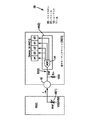
この点について、図1は、電子デバイスとして共通通信バス16に通信可能に結合された1つのマスタデバイス12と4つのスレーブデバイス14(1)〜14(4)とを有する例示的なシステム10のブロック図である。マスタデバイス12は、通信バス16を介してスレーブデバイス14(1)〜14(4)と通信する。したがって、システム10では、データ衝突を回避するために、時分割多重(TDM:time division multiplexed)フレーム構造が、通信バス16を介するビットレートメディアストリームの搬送のために使用される。マスタデバイス12は、バス通信のためにスレーブデバイス14(1)〜14(4)の各々に送信タイムスロットを割り当てる。したがって、プロトコルは、「Device_Id」とも呼ばれるデバイス識別情報を介して、スレーブデバイス14(1)〜14(4)の各々が通信バス16に接続されていることがマスタデバイス12によって確認されることを必要とする。たとえば、Device_Idは、たとえば、5ビットなどの、プロトコルにおいて指定されたビット長を有してもよい。スレーブデバイス14(1)〜14(4)の異なるDevice_Idを識別することは、マスタデバイス12が、通信バス16におけるデータ衝突を回避するために、スレーブデバイス14(1)〜14(4)の各々に異なる送信タイムスロットを割り当てることを可能にする。
In this regard, FIG. 1 illustrates an
Device_Idは、電子デバイスを識別するために使用されるべきデフォルトのデバイス識別情報として製造業者によって電子デバイス内にロードされることになる。たとえば、図1に示すように、Device_Id26(1)は、マスタデバイス12内にロードされることが可能である。Device_Id28(1)〜28(4)は、それぞれのスレーブデバイス14(1)〜14(4)内にロードされることが可能である。しかしながら、同じDevice_Id28は、異なるスレーブデバイス14(1)〜14(4)内にロードされる可能性がある。この場合には、同じDevice_Id28を有するスレーブデバイス14(1)〜14(4)は、同じDevice_Id28を有するマスタデバイス12によって識別されることになり、通信バス16上でデータ衝突を引き起こす。各スレーブデバイス14(1)〜14(4)が固有のDevice_Id28(1)〜28(4)を有することを確実にする1つの方法は、各スレーブデバイス14(1)〜14(4)が製造時に固有のDevice_Idをロードされることを確実にすることである。同じ製造業者によって製造された複数のスレーブデバイスは、同じデバイス識別情報を有する場合がある。固有のDevice_Id28を提供することは、より大きいデバイス識別情報記憶設備を必要とすることになり、それは、そうでなければ低コストのデバイスのコストを法外に増加させる。さらにスレーブデバイス14(1)〜14(4)が異なる製造業者によって製造された場合でも、各製造業者がそれらのスレーブデバイスにおいて固有のデバイス識別情報を用いることを保証することは、困難または不可能である可能性がある。
Device_Id will be loaded into the electronic device by the manufacturer as default device identification information to be used to identify the electronic device. For example, Device_Id 26 (1) can be loaded into the master device 12, as shown in FIG. Device_Id 28 (1) -28 (4) can be loaded into each slave device 14 (1) -14 (4). However, the
したがって、費用効果的な方法でデータ衝突を回避するために、スレーブ電子デバイスの固有の識別を可能にするために、共通通信バスを用いる通信システムにおいて設けられる電子デバイスのための固有のデバイス識別情報を提供することが望ましい。 Thus, unique device identification information for electronic devices provided in a communication system using a common communication bus to allow unique identification of slave electronic devices to avoid data collisions in a cost effective manner It is desirable to provide
詳細な説明で開示される態様は、バス通信識別のためのデバイス識別情報の選択または再プログラムなどの外部制御を可能にするための、電子デバイスにおけるデバイス識別情報の生成を含む。関連するシステムおよび方法も開示される。このようにして、システムにおける共通通信バスに結合された電子デバイスのデバイス識別情報は、バス通信の衝突を回避するためにデバイス識別情報が固有であることを保証するために、選択または再プログラムされることが可能である。たとえば、バス通信システムでは、バス通信プロトコルは、それに結合された電子デバイスがデバイス識別情報を介してマスタ電子デバイスによって識別されることを必要としてもよい。デバイス識別情報は、通信バス上のデータ衝突を回避するために、スレーブデバイスの各々への異なる送信タイムスロットの割り当てを制御するために使用される。2つ以上のスレーブデバイスが同じデバイス識別情報を有する場合、マスタデバイスは、そのようなスレーブデバイスに対して同じ送信タイムスロットを割り当てることになり、それによって、バス通信の衝突を引き起こす。 Aspects disclosed in the detailed description include generation of device identification information in an electronic device to allow external control such as selection or reprogramming of device identification information for bus communication identification. Related systems and methods are also disclosed. In this way, the device identification information of electronic devices coupled to a common communication bus in the system is selected or reprogrammed to ensure that the device identification information is unique to avoid bus communication collisions. Is possible. For example, in a bus communication system, the bus communication protocol may require that an electronic device coupled thereto be identified by the master electronic device via device identification information. The device identification information is used to control the assignment of different transmission time slots to each of the slave devices in order to avoid data collisions on the communication bus. If two or more slave devices have the same device identification information, the master device will assign the same transmission time slot to such slave devices, thereby causing a bus communication collision.
本明細書で開示された特定の態様では、電子デバイスにおけるデバイス識別情報を選択または再プログラムするために、外部ソースが提供される。非限定的な例として、デバイス識別情報が選択または再プログラムされる電子デバイスは、システムにおけるスレーブデバイスであってもよい。外部ソースは、電子デバイス内のデバイス識別情報生成回路とともに回路を閉じるために、電子デバイスに電気的に結合されることが可能である。外部ソースによって閉じられた回路は、電子デバイス内のデバイス識別情報生成回路によって検出可能な所望の電気的特性(たとえば、電圧、抵抗、容量)を提供する。デバイス識別情報生成回路は、外部ソースによって閉じられた回路の検出された電気的特性の関数としてデバイス識別情報を生成するように構成される。これは、外部ソースが、閉じられた回路の電気的特性を制御することに基づいて、電子デバイスのデバイス識別情報を所望のデバイス識別情報に外部的に選択または再プログラムすることを可能にする。したがって、電子デバイスの製造業者以外のエンティティ(たとえば、アグリゲータ)は、電子デバイス内のデバイス識別情報生成回路にその電子デバイス内に記憶されたデバイス識別情報を選択または再プログラムさせるように外部ソースを制御することができる。このようにして、システム内の共通通信バスに結合されたスレーブデバイスのデバイス識別情報の一意性は、バス通信の衝突を回避するために、必要に応じて提供されることが可能である。 In certain aspects disclosed herein, an external source is provided for selecting or reprogramming device identification information in an electronic device. As a non-limiting example, the electronic device for which device identification information is selected or reprogrammed may be a slave device in the system. An external source can be electrically coupled to the electronic device to close the circuit along with a device identification information generation circuit within the electronic device. Circuits closed by external sources provide desired electrical characteristics (eg, voltage, resistance, capacitance) that can be detected by device identification information generation circuitry within the electronic device. The device identification information generation circuit is configured to generate device identification information as a function of the detected electrical characteristics of the circuit closed by the external source. This allows an external source to externally select or reprogram the device identification information of the electronic device to the desired device identification information based on controlling the electrical characteristics of the closed circuit. Thus, an entity other than the electronic device manufacturer (e.g., an aggregator) controls the external source to cause the device identification information generation circuit in the electronic device to select or reprogram the device identification information stored in the electronic device. can do. In this way, the uniqueness of the device identification information of slave devices coupled to a common communication bus in the system can be provided as needed to avoid bus communication conflicts.
この点について、一態様では、そのデバイス識別情報を再プログラムするように構成された電子デバイスが提供される。電子デバイスは、通信バスに結合されるように構成されたデバイス識別ポートを備える。電子デバイスはまた、デバイス識別ポートに結合されたデバイス識別情報生成回路を備える。デバイス識別情報生成回路は、デバイス識別ポート上で通信バスから受信した通信バス信号の電気的特性を検出するように構成される。デバイス識別情報生成回路はまた、検出された電気的特性に基づいてデバイス識別情報を生成するように構成される。デバイス識別情報生成回路はまた、生成されたデバイス識別情報をデバイス識別情報メモリ内に記憶するように構成される。 In this regard, in one aspect, an electronic device is provided that is configured to reprogram its device identification information. The electronic device includes a device identification port configured to be coupled to a communication bus. The electronic device also includes a device identification information generation circuit coupled to the device identification port. The device identification information generation circuit is configured to detect an electrical characteristic of the communication bus signal received from the communication bus on the device identification port. The device identification information generation circuit is also configured to generate device identification information based on the detected electrical characteristics. The device identification information generation circuit is also configured to store the generated device identification information in a device identification information memory.
別の態様では、電子デバイスであって、そのデバイス識別情報を再プログラムするように構成された電子デバイスが提供される。電子デバイスは、通信バスに結合するために構成されたデバイス識別手段を備える。電子デバイスはまた、デバイス識別手段に結合されたデバイス識別情報生成手段を備える。デバイス識別情報生成手段は、デバイス識別手段において通信デバイスから受信した通信バス信号の電気的特性を検出するための手段を備える。デバイス識別情報生成手段はまた、検出された電気的特性に基づいてデバイス識別情報を生成するための手段を備える。デバイス識別情報生成手段はまた、生成されたデバイス識別情報をデバイス識別情報メモリ内に記憶するための手段を備える。 In another aspect, an electronic device is provided that is configured to reprogram its device identification information. The electronic device comprises device identification means configured for coupling to a communication bus. The electronic device also comprises device identification information generating means coupled to the device identification means. The device identification information generating means includes means for detecting an electrical characteristic of the communication bus signal received from the communication device in the device identification means. The device identification information generating means also includes means for generating device identification information based on the detected electrical characteristics. The device identification information generating means also includes means for storing the generated device identification information in a device identification information memory.
別の態様では、電子デバイスがそのデバイス識別情報を再プログラムするための方法が提供される。方法は、通信バスに結合されたデバイス識別ポートにおいて通信バスから受信した通信バス信号の電気的特性を検出するステップを備える。方法はまた、通信バス信号の検出された電気的特性に基づいてデバイス識別情報を生成するステップを備える。方法はまた、生成されたデバイス識別情報をデバイス識別情報メモリ内に記憶するステップを備える。 In another aspect, a method is provided for an electronic device to reprogram its device identification information. The method comprises detecting an electrical characteristic of a communication bus signal received from the communication bus at a device identification port coupled to the communication bus. The method also comprises generating device identification information based on the detected electrical characteristics of the communication bus signal. The method also comprises storing the generated device identification information in a device identification information memory.
別の態様では、通信バスに結合されたスレーブデバイスがそのデバイス識別情報を再プログラムすることを可能にするためのバス通信システムが提供される。バス通信システムは、データ線とクロック線とから構成された通信バスを備える。バス通信システムはまた、マスタデータポートとマスタクロックポートとから構成されたマスタデバイスを備え、マスタデバイスは、データ線に結合されたマスタデータポートと、クロック線に結合されたマスタクロックポートとによって、通信バスに結合される。バス通信システムはまた、複数のスレーブデバイスを備える。複数のスレーブデバイスの各々は、通信バスに結合されたデータポートとクロックポートとを備え、データポートおよびクロックポートのうちの少なくとも1つはまた、デバイス識別ポートを備える。データポートは、通信バスのデータ線に結合され、クロックポートは、通信バスのクロック線に結合される。複数のスレーブデバイスの各々はまた、デバイス識別ポートに結合されたデバイス識別情報生成回路を備える。デバイス識別情報生成回路は、デバイス識別ポート上で通信バスから受信した通信バス通信の電気的特性を検出するように構成される。デバイス識別情報生成回路はまた、検出された電気的特性に基づいてデバイス識別情報を生成するように構成される。デバイス識別情報生成回路はまた、生成されたデバイス識別情報をデバイス識別情報メモリ内に記憶するように構成される。 In another aspect, a bus communication system is provided for allowing a slave device coupled to a communication bus to reprogram its device identification information. The bus communication system includes a communication bus composed of a data line and a clock line. The bus communication system also includes a master device composed of a master data port and a master clock port, the master device comprising a master data port coupled to the data line and a master clock port coupled to the clock line. Coupled to a communication bus. The bus communication system also includes a plurality of slave devices. Each of the plurality of slave devices includes a data port and a clock port coupled to the communication bus, and at least one of the data port and the clock port also includes a device identification port. The data port is coupled to the data line of the communication bus, and the clock port is coupled to the clock line of the communication bus. Each of the plurality of slave devices also includes a device identification information generation circuit coupled to the device identification port. The device identification information generation circuit is configured to detect an electrical characteristic of the communication bus communication received from the communication bus on the device identification port. The device identification information generation circuit is also configured to generate device identification information based on the detected electrical characteristics. The device identification information generation circuit is also configured to store the generated device identification information in a device identification information memory.
ここで図面を参照して、本開示のいくつかの例示的な態様を説明する。「例示的」という語は、本明細書では「一例、事例、または例示として挙げること」を意味するために使用される。「例示的」なものとして本明細書で説明されるいずれの態様も、必ずしも他の態様よりも好ましい、または有利であると解釈されるわけではない。 Several exemplary aspects of the present disclosure will now be described with reference to the drawings. The word “exemplary” is used herein to mean “giving as an example, instance, or illustration”. Any aspect described herein as "exemplary" is not necessarily to be construed as preferred or advantageous over other aspects.
詳細な説明で開示される態様は、バス通信識別のためのデバイス識別情報の選択または再プログラムなどの外部制御を可能にするための、電子デバイスにおけるデバイス識別情報生成を含む。関連するシステムおよび方法も開示される。このようにして、システム内の共通通信バスに結合された電子デバイスのデバイス識別情報は、バス通信の衝突を回避するために、デバイス識別情報が固有であることを確実にするために、選択または再プログラムされることが可能である。たとえば、バス通信システムにおいて、バス通信プロトコルは、それに結合された電子デバイスがデバイス識別情報を介してマスタ電子デバイスによって識別されることを必要とする。デバイス識別情報は、通信バス上のデータ衝突を回避するために、スレーブデバイスの各々への異なる送信タイムスロットの割り当てを制御するために使用される。2つ以上のスレーブデバイスが同じデバイス識別情報を有する場合、マスタデバイスは、そのようなスレーブデバイスに対して同じ送信タイムスロットを割り当てることになり、それによって、バス通信の衝突を引き起こす。 Aspects disclosed in the detailed description include device identification information generation in an electronic device to allow external control such as selection or reprogramming of device identification information for bus communication identification. Related systems and methods are also disclosed. In this way, the device identification information of the electronic devices coupled to the common communication bus in the system is selected or ensured that the device identification information is unique to avoid bus communication collisions. It can be reprogrammed. For example, in a bus communication system, the bus communication protocol requires that the electronic device coupled to it be identified by the master electronic device via device identification information. The device identification information is used to control the assignment of different transmission time slots to each of the slave devices in order to avoid data collisions on the communication bus. If two or more slave devices have the same device identification information, the master device will assign the same transmission time slot to such slave devices, thereby causing a bus communication collision.
本明細書に開示された特定の態様では、電子デバイスにおいてデバイス識別情報を選択または再プログラムするために、外部ソースが提供される。非限定的な例として、そのデバイス識別情報が選択または再プログラムされる電子デバイスは、システム内のスレーブデバイスであってもよい。外部ソースは、電子デバイス内のデバイス識別情報生成回路とともに回路を閉じるために、電子デバイスに電気的に結合されることが可能である。外部ソースによって閉じられた回路は、電子デバイス内のデバイス識別情報生成回路によって検出可能な所望の電気的特性(たとえば、電圧、抵抗値、静電容量)を提供する。デバイス識別情報生成回路は、外部ソースによって閉じられた回路の検出された電気的特性の関数としてデバイス識別情報を生成するように構成される。これは、外部ソースが、閉じられた回路の電気的特性を制御することに基づいて、電子デバイスのデバイス識別情報を所望の識別情報に外部的に選択または再プログラムすることを可能にする。したがって、電子デバイスの製造業者以外のエンティティ(たとえば、アグリゲータ)は、電子デバイス内のデバイス識別情報生成回路にその電子デバイス内に記憶されたデバイス識別情報を選択または再プログラムさせるように外部ソースを制御することができる。このようにして、システム内の共通通信バスに結合されたスレーブデバイスのデバイス識別情報の一意性は、バス通信の衝突を回避するために、必要に応じて提供されることが可能である。 In certain aspects disclosed herein, an external source is provided for selecting or reprogramming device identification information in an electronic device. As a non-limiting example, the electronic device whose device identification information is selected or reprogrammed may be a slave device in the system. An external source can be electrically coupled to the electronic device to close the circuit along with a device identification information generation circuit within the electronic device. Circuits closed by external sources provide the desired electrical characteristics (eg, voltage, resistance, capacitance) that can be detected by device identification information generation circuitry within the electronic device. The device identification information generation circuit is configured to generate device identification information as a function of the detected electrical characteristics of the circuit closed by the external source. This allows an external source to externally select or reprogram the device identification information of the electronic device to the desired identification information based on controlling the electrical characteristics of the closed circuit. Thus, an entity other than the electronic device manufacturer (e.g., an aggregator) controls the external source to cause the device identification information generation circuit in the electronic device to select or reprogram the device identification information stored in the electronic device. can do. In this way, the uniqueness of the device identification information of slave devices coupled to a common communication bus in the system can be provided as needed to avoid bus communication conflicts.
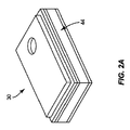
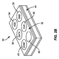
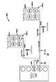
この点について、図2Aは、この例ではオーディオ電子デバイスである、バス通信デバイスの形態における例示的な電子デバイス30の上面斜視図である。電子デバイス30は、プロトコルベースのメッセージを受信および通信するように構成される。電子デバイス30は、通信バスを有するシステム内のスレーブデバイスとして提供されてもよい。図2Bは、例示的なピンアウト構成を示す、図2A中の例示的な電子デバイス30の底面斜視図である。図2Bに示すように、電子デバイス30は、電気的接続が電子デバイス30に対してなされることを可能にする外部ピン32を含む。たとえば、外部電源(図示せず)は、電子デバイス30にその動作のために電力を提供するために、電源ピン34および接地ピン36に結合されてもよい。図2B中の電子デバイス30はまた、電子デバイス30がオーディオデータを受信することを可能にするために通信バスのそれぞれのデータ線およびクロック線に結合されるように各々が構成された、データポートとしてのデータピン38とクロックポートとしてのクロックピン40とを含む。たとえば、電子デバイス30のデータピン38およびクロックピン40は、図1中の通信バス16などの通信バスのデータ線およびクロック線に結合されるように構成される。また、外部プルアップまたはプルダウン抵抗器(図示せず)への接続がステレオシステムのための左または右マイクロホンのいずれかであるように電子デバイス30を構成することを可能にするために、会議(conference)ピン42が、レガシーピンとして電子デバイス30内に設けられてもよい。電子デバイス30のデータピン38に向かう通信バス上のオーディオデータは、したがって、会議ピン42に接続された外部プルアップまたはプルダウン抵抗器の示す値に基づいて、左または右オーディオチャネルのいずれかのオーディオであることになる。
In this regard, FIG. 2A is a top perspective view of an exemplary
図2Aおよび図2Bを引き続き参照すると、電子デバイス30が通信バスに接続されたときに識別されることを可能にすることが望ましいことがある。この点について、電子デバイス30は、本明細書では「Device_Id44」とも呼ばれる内部デバイス識別情報メモリ44を含む。Device_Id44は、識別番号または他の標識を記憶することができる記憶設備である。たとえば、Device_Id44は、デバイス識別情報として2進数を提供するように構成された複数のビットから構成されてもよい。電子デバイス30はまた、複数のデバイス識別情報を含んでもよい。しかしながら、Device_Id44は、電子デバイス30と同じ通信バスに結合された別の電子デバイスと同じデバイス識別情報をロードされている可能性がある。この場合、上記で説明したように、通信バスに結合された別の電子デバイスと同じDevice_Id44を有する電子デバイス30は、同じデバイス識別情報で識別されることになり、それによって、通信バス上のデータ衝突を引き起こす。電子デバイス30が固有のDevice_Id44を有することを確実にする1つの方法は、必要に応じて、固有のデバイス識別情報でデフォルトのDevice_Id44を再プログラムする能力を有することである。
With continued reference to FIGS. 2A and 2B, it may be desirable to allow
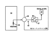
この点について、図2Bおよび図3に示すように、電子デバイス30は、Device_Id44が再プログラムされることを可能にするデバイス識別ポートを提供するために、追加の外部ピン46を伴って構成される。この例では、追加の外部ピン46は、デバイス識別ピンである。図3に示すように、この例における電子デバイス30内のDevice_Id44は、ビットd0として長さが1の2値ビットである。したがって、電子デバイス30は、Device_Id44として2つ(すなわち、21=2)の異なるデバイス識別情報でプログラムされることが可能である。電子デバイス30のDevice_Id44が再プログラムされることを可能にするために、電子デバイス30は、デバイス識別情報生成回路48を含む。デバイス識別情報生成回路48は、追加の外部ピン46に結合される。この例では外部抵抗器56である外部ソース50は、デバイス識別情報生成回路48とともに回路52を形成するために、追加の外部ピン46に接続される。外部抵抗器56によって形成された回路52は、電子デバイス30内のデバイス識別情報生成回路48によって検出可能な所望の抵抗値を提供する。デバイス識別情報生成回路48は、外部抵抗器56の抵抗レベルに基づいて「1」または「0」のデジタル値を生成するように構成されたバッファ回路57を含む。このようにして、外部ソース50は、外部抵抗器56の抵抗値に基づいて、電子デバイス30のDevice_Id44を所望のデバイス識別情報に外部的にプログラムまたは再プログラムすることができる。また、別の例として、デバイス識別情報生成回路48はまた、電子デバイス30内に設けられた複数のデバイス識別情報から選択された電子デバイス30内のデバイス識別情報を再プログラムするように構成されることが可能である。
In this regard, as shown in FIGS. 2B and 3, the
したがって、外部ソース50を使用することによって、たとえば、アグリゲータなどの、電子デバイス30の製造業者以外のエンティティは、電子デバイス30内のデバイス識別情報生成回路48にDevice_Id44をプログラムまたは再プログラムさせるように外部ソース50を制御することができる。このようにして、電子デバイス30のDevice_Id44の一意性は、バス通信の衝突を回避するために、電子デバイス30を識別する共通通信バスを用いるシステムにおいて用いられたとき、制御されることが可能である。
Thus, by using an
図3中の電子デバイス30において、追加の外部ピン46は、外部ソース50をデバイス識別情報生成回路48に結合するために設けられる。しかしながら、この解決策は、外部ピンが電子デバイス30上に設けられることを必要とする。外部ソースがオーディオデバイス内のデバイス識別情報を再プログラムできるようにすることを可能にするために電子デバイスに外部ピンを追加することが望ましくない場合がある。外部ソースを使用してそのデバイス識別情報を再プログラムすることを可能にしながら、電子デバイスに追加の外部ピンを追加することを回避する1つの技術は、オーディオデバイスの別の既存のピンに外部ソースを結合することである。たとえば、外部ソースは、図2Bに示すように、電子デバイス30の会議ピン42に結合されることが可能であり、会議ピン42は、デバイス識別ポートとして再利用される。この例では、会議ピン42は、デバイス識別ピンを提供する。会議ピン42は、左または右オーディオチャネルのいずれかを検出するその元の目的のために使用される代わりに、電子デバイス30内のデバイス識別情報を再プログラムするためにデバイス識別ポートとして使用されるためにプルアップまたはプルダウン抵抗器に結合されるように構成されるように電子デバイス30上に設けられてもよい。
In the
この点について、図4Aは、別の例示的な電子デバイス30(1)を示す。電子デバイス30(1)は、図2A〜図3と図4Aとの間で共通の番号でラベル付けされた共通の要素を有する図2A〜図3中の電子デバイス30と同様である。図4A中の電子デバイス30(1)は、電子デバイス30(1)のDevice_Id44(1)が再プログラムされることを可能にするデバイス識別情報生成回路48(1)を含む。デバイス識別情報生成回路48(1)は、電子デバイス30(1)の既存の会議ピン42に、この例では外部可変電圧源50(1)である外部ソースによって印加される可変電圧Vrefに基づいて、新たなDevice_Id44(1)を生成するように構成される。回路52(1)は、可変電圧Vrefが電子デバイス30(1)内のデバイス識別情報生成回路48(1)によって検出されることを可能にする外部ソース50(1)によって形成される。
In this regard, FIG. 4A shows another exemplary electronic device 30 (1). Electronic device 30 (1) is similar to
図4Aに示すように、この例における電子デバイス30(1)内のDevice_Id44(1)は、ビットd4〜d0として長さ5の2値ビットから構成された多ビットデバイス識別情報メモリである。したがって、電子デバイス30(1)は、Device_Id44(1)として32(すなわち、25=32)の異なるデバイス識別情報でプログラムされることが可能である。デバイス識別情報生成回路48(1)は、可変電圧Vrefの振幅(すなわち、電圧レベル)に基づいてデジタル値を生成するように構成されたアナログ-デジタル変換器(ADC:analog-to-digital converter)54を含む。可変電圧Vrefは、ADC54によって異なる電圧範囲に分割される。このようにして、外部ソース50(1)は、可変電圧Vrefの電圧レベルを制御することに基づいて、電子デバイス30(1)のDevice_Id44(1)を所望のデバイス識別情報に外部的にプログラムまたは再プログラムすることができる。
As shown in FIG. 4A, Device_Id 44 (1) in the electronic device 30 (1) in this example is a multi-bit device identification information memory composed of binary bits of
したがって、外部ソース50(1)を使用することによって、たとえば、アグリゲータなどの、電子デバイス30(1)の製造業者以外のエンティティは、電子デバイス30(1)内のデバイス識別情報生成回路48(1)にDevice_Id44(1)をプログラムまたは再プログラムさせるように外部ソース50(1)を制御することができる。このようにして、電子デバイス30(1)のDevice_Id44(1)の一意性は、バス通信の衝突を回避するために、スレーブデバイスを識別する共通通信バスを用いるシステムにおいて用いられたとき、制御されることが可能である。 Thus, by using the external source 50 (1), an entity other than the manufacturer of the electronic device 30 (1), such as an aggregator, for example, can generate a device identification information generation circuit 48 (1 ) Can control the external source 50 (1) to program or reprogram Device_Id44 (1). In this way, the uniqueness of Device_Id44 (1) of electronic device 30 (1) is controlled when used in a system that uses a common communication bus that identifies slave devices to avoid bus communication conflicts. Is possible.
可変電圧Vrefの電圧レベルに基づいてDevice_Id44(1)を生成するために、ADC54以外の回路が図4A中の電子デバイス30(1)内に設けられてもよいことに留意されたい。非限定的な例は、演算増幅器と、内部抵抗器と、内部キャパシタとを含む。
Note that circuitry other than
図4Aを引き続き参照すると、デバイス識別情報生成回路48(1)は、Device_Id44(1)のビットd4〜d0のすべてまたはサブセットを再プログラムするように構成されることが可能である。たとえば、電子デバイス30(1)内のデバイス識別情報生成回路48(1)内のADC54は、図4Aにおいて一例として、ビットd2〜d0に結合されるように示されている。したがって、このシナリオにおけるデバイス識別情報生成回路48(1)は、Device_Id44(1)のすべてよりも少ないビットd4〜d0を再プログラムするように構成される。これは、電子デバイス30(1)のための固有のデバイス識別情報を提供するために、Device_Id44(1)のビットのすべてをプログラムできることが必要とされないので、有利である場合がある。たとえば、ビットd4およびd3が電子デバイス30(1)のタイプを識別するために電子デバイス30(1)の製造業者によってデフォルトの値でプログラムされることのみが可能であるプレフィクス値である標準に従うことができる。たとえば、表59に示すように、ビットd4およびd3が「00」でプログラムされた場合、これは、電子デバイス30(1)がマイクロホンであることを意味するとみなされることが可能である。表59に示すように、ビットd4およびd3が「01」でプログラムされた場合、これは、電子デバイス30(1)がスピーカであることを意味するとみなされることが可能である。表59に示すように、ビットd4およびd3が「10」でプログラムされた場合、これは、電子デバイス30(1)がコーデックであることを意味するとみなされることが可能である。表59に示すように、ビットd4およびd3が「11」でプログラムされた場合、これは、電子デバイス30(1)が別のオーディオデバイスであることを意味するとみなされることが可能である。これは、この例におけるADC54が、より少ないアナログ値をデジタル値に変換することができるより低コストのデバイスであることが可能であるという点で、コストを節約することができる。
With continued reference to FIG. 4A, device identification information generation circuit 48 (1) may be configured to reprogram all or a subset of bits d4-d0 of Device_Id 44 (1). For example, the
図4Bは、電子デバイス30(2)の外部会議ピン42に適用される外部可変抵抗器56(1)の可変抵抗値Rrefに基づいて新たなDevice_Id44(1)を生成するように構成されたデバイス識別情報生成回路48(2)を有する電子デバイス30(2)の別の例の概略図である。電子デバイス30(2)は、図2A〜図4Aと図4Bとの間で共通の番号でラベル付けされた共通の要素を有する図2A〜図4A中の電子デバイス30、30(1)と同様である。この例では、電子デバイス30(1)のデバイス識別情報生成回路48(1)に可変電圧Vrefを印加する図4A中の外部ソース50(1)の代わりに、会議ピン42に外部可変抵抗器56(1)の可変抵抗値Rrefを適用するように構成された代替の外部ソース50(2)が、図4Bにおいて提供される。外部ソース50(2)は、外部可変抵抗器56(1)に正の電力レール(Vdd)または接地(Vss)のいずれかを適用するように構成される。外部可変抵抗器56(1)の可変抵抗値Rrefは、可変電圧Vrefを生成するために、外部可変抵抗器56(1)にわたる電圧を分割する分圧器と、電子デバイス30(2)内の内部抵抗器Rinとを提供する回路52(2)を形成することになる。図4A中の電子デバイス30(1)と同様に、デバイス識別情報生成回路48(2)のADC54は、可変電圧Vrefの振幅(すなわち、電圧レベル)に基づいてデジタル値を生成するように構成される。可変電圧Vrefは、ADC54によって異なる電圧範囲に分割される。このようにして、外部ソース50(2)は、可変電圧Vrefの電圧レベルを制御することに基づいて、電子デバイス30(2)のDevice_Id44(1)を所望のデバイス識別情報に外部的にプログラムまたは再プログラムすることができる。
FIG.4B shows a device configured to generate a new Device_Id44 (1) based on the variable resistance value Rref of the external variable resistor 56 (1) applied to the
図4Cは、電子デバイス30(3)の会議ピン42に適用される外部可変キャパシタ58(1)の静電容量Crefに基づいて新たなDevice_Id44(1)を生成するように構成されたデバイス識別情報生成回路48(3)を有する電子デバイス30(3)の別の例の概略図である。電子デバイス30(3)は、図2A〜図4Aと図4Cとの間で共通の番号でラベル付けされた共通の要素を有する図2A〜図4A中の電子デバイス30、30(1)と同様である。この例では、電子デバイス30(2)のデバイス識別情報生成回路48(2)に可変電圧Vrefを印加する図4B中の外部ソース50(2)の代わりに、会議ピン42に外部可変キャパシタ58(1)の可変静電容量Crefを適用するように構成された代替の外部ソース50(3)が、図4Cにおいて提供される。外部ソース50(3)は、外部可変キャパシタ58(1)に電力レール(Vdd)または接地(Vss)のいずれかを適用するように構成される。外部可変キャパシタ58(1)の可変静電容量Crefは、外部可変キャパシタ58(1)の可変静電容量Crefをデバイス識別情報生成回路48(3)に結合する回路52(3)を形成することになる。デバイス識別情報生成回路48(3)は、外部可変キャパシタ58(1)の充電時間を測定することによって、可変静電容量Crefを検出するように構成される。検出された可変静電容量Crefは、外部可変キャパシタ58(1)の可変静電容量Crefに基づいてデジタル値を生成するために、デバイス識別情報生成回路48(3)のADC54によって使用されることが可能である。
FIG. 4C shows device identification information configured to generate a new Device_Id 44 (1) based on the capacitance Cref of the external variable capacitor 58 (1) applied to the
図4A〜図4C中の電子デバイス30(1)〜30(3)の他の例では、電子デバイス30は、抵抗値、インダクタンス、または静電容量以外の別の電気的特性に基づいて新たなDevice_Id44を生成するように構成された代替のデバイス識別情報生成回路48を設けられることが可能であることに留意されたい。たとえば、電気的特性は、外部ソース50によって電子デバイス30のデバイス識別情報生成回路48に適用される外部信号の周波数であってもよい。たとえば、外部信号は、以下で説明するように、データ信号またはクロック信号を含む通信バス信号であってもよい。デバイス識別情報生成回路48は、そのような周波数に基づいてデジタル値を生成するためにADC54によって使用されるべき外部信号の周波数を測定するように構成されることが可能である。
In other examples of electronic devices 30 (1) -30 (3) in FIGS. 4A-4C, the
電子デバイスが、電子デバイスのためのデバイス識別情報として、製造業者によるような、事前に電子デバイス内にプログラムされたあらかじめ定義されたデバイス識別子を選択することを可能にすることを望ましい場合もある。この機能は、上記で説明した電子デバイス30〜30(3)内に提供されるように、そのデバイス識別情報が再プログラムされることを可能にするように構成されている電子デバイスの代わりに、またはそれに加えて提供されることが可能である。この点について、図4Dは、デバイス識別ポートとして提供されるデバイス識別ピンとしての会議ピン42に適用される電気的特性に基づいて電子デバイス30(4)を識別するために使用されるべきデバイス識別情報を選択するように構成された代替の電子デバイス30(4)の概略図である。図4D中の外部ソース50(4)が回路52(4)において検出されることが可能な電気的特性を生成することができる方法は、上記およびそこで説明した例のいずれかにおいて提供されるのと同じであることが可能である。よって、説明は繰り返さない。
It may be desirable to allow an electronic device to select a pre-defined device identifier programmed in advance in the electronic device, such as by the manufacturer, as device identification information for the electronic device. This function, instead of an electronic device configured to allow its device identification information to be reprogrammed, as provided in the electronic devices 30-30 (3) described above, Or it can be provided in addition. In this regard, FIG. 4D shows the device identification to be used to identify the electronic device 30 (4) based on the electrical characteristics applied to the
しかしながら、図4D中の電子デバイス30(4)では、デバイス識別情報選択回路55が、デバイス識別情報生成回路の代替として設けられる。デバイス識別情報選択回路55は、上記で説明したデバイス識別情報生成回路48〜48(3)と同様のADC54を含む。会議ピン42上の外部ソース50(4)によって生成された電気的特性は、デバイス識別情報選択回路55によって検出されることが可能である。デバイス識別情報選択回路55のADC54は、デバイス識別情報選択回路55によって検出された電気的特性に基づいてデジタル値を生成するように構成される。ADC54は、低コストADCであってもよい。各々があらかじめ記憶されたDevice_Id44(2)〜44(5)を有する複数のデバイス識別子Id3〜Id0のうちの1つを選択するために複数のデコーダ線61のうちの1つを選択するために、ADC54によって生成されたデジタル値を受信し、使用するように構成されたデコーダ63が、デバイス識別情報選択回路55内に設けられる。一態様では、Device_Id44(2)〜44(5)の各々は、他に対して固有である。デバイス識別子Id3〜Id0の各々は、所望の任意のビット数で構成されてもよい。選択されたデバイス識別子Id3〜Id0は、電子デバイス30(4)のためのデバイス識別情報として使用されることが可能である。この例では、4つのDevice_Id44(2)〜44(5)が存在するので、デコーダ63は、2-4デコーダであり、デコーダ63は、ADC54から2ビットデジタル値を受信するように構成される。
However, in the electronic device 30 (4) in FIG. 4D, the device identification
したがって要約すると、図4Dの電子デバイス30(4)では、デバイス識別情報は、この例では再プログラム可能でないが、選択可能な複数のDevice_Id44(2)〜44(5)を提供することによって、それ自体を識別するために電子デバイス30(4)によって使用されるべきデバイス識別情報は、外部ソース50(4)を介して選択されることが可能である。デバイス識別情報を再プログラムまたは選択させるために、上記で説明した電子デバイス30〜30(4)などの電子デバイスに適用される外部ソースはまた、再プログラムされるべき電子デバイスとともに共通通信バスに結合された別の電子デバイスによって提供されることが可能である。 Therefore, in summary, in the electronic device 30 (4) of FIG. 4D, the device identification information is not reprogrammable in this example, but by providing multiple selectable Device_Ids 44 (2) -44 (5) Device identification information to be used by electronic device 30 (4) to identify itself can be selected via external source 50 (4). An external source applied to an electronic device, such as electronic device 30-30 (4) described above, is also coupled to the common communication bus along with the electronic device to be reprogrammed to cause device identification information to be reprogrammed or selected. Provided by another electronic device.
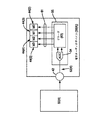
この点について、図5は、例示的なバス通信システム60(1)の概略図である。バス通信システム60(1)は、通信バス66に結合された例示的なスレーブデバイス62(1)〜62(N)とマスタデバイス64とを含み、ここで「N」は、スレーブデバイス62の数を表す。マスタデバイス64および/またはスレーブデバイス62(1)〜62(N)は、非限定的な例として、別々の構成要素内に設けられてもよく、または同じ回路基板上に配置されてもよい。図5中のバス通信システム60(1)は、例示的なシステムであるが、バス通信システム60(1)はまた、システムのプロトコルの一部として通信バスに結合されたスレーブデバイスのデバイス識別情報を要求する通信バスを含む任意の他のシステムであってもよい。スレーブデバイス62(1)〜62(N)の各々は、上記で説明したデバイス識別情報生成回路と同様であることが可能なデバイス識別情報生成回路48(1)〜48(N)を有する。
In this regard, FIG. 5 is a schematic diagram of an exemplary bus communication system 60 (1). Bus communication system 60 (1) includes exemplary slave devices 62 (1) -62 (N) and
図5を引き続き参照すると、デバイス識別情報生成回路48(1)〜48(N)は、通信バス信号65に適用される可変電圧Vref(1)〜Vref(N)に基づいて、それらのそれぞれのスレーブデバイス62(1)〜62(N)のための新たなDevice_Id(図示せず)を生成するように構成される。この例では、スレーブデバイス62(1)〜62(N)のための新たなDevice_Idを生成するために使用される通信バス信号65は、通信バスクロック信号67である。通信バスクロック信号67は、通信バス66の共通クロック線70に結合された外部プルアップまたはプルダウン抵抗器Rext(1)〜Rext(N)の結果として、それぞれのスレーブデバイス62(1)〜62(N)の既存のクロックピン68(1)〜68(N)上でアサートされる。可変電圧Vref(1)〜Vref(N)は、クロック線70に適用される通信バスクロック信号67の一定のトグリングレート(toggling rate)の結果として生成され、クロック線70は、クロックピン68(1)〜68(N)と、マスタクロックピン72として設けられたマスタクロックポートとに結合される。通信バスクロック信号67の直流(DC)成分が、固有の可変電圧Vref(1)〜Vref(N)を生成するために外部抵抗器Rext(1)〜Rext(N)に適用されるように、交流(AC)結合74(1)〜74(N)は、通信バスクロック信号67のAC成分をフィルタリングするために設けられ、クロック線70に結合される。この点について、外部抵抗器Rext(1)〜Rext(N)は、固有のデバイス識別情報(たとえば、Device_Id)を生成するために、デバイス識別情報生成回路48(1)〜48(N)内のADCに異なるデジタル出力値を生成させるように可変電圧Vref(1)〜Vref(N)にさせる固有の抵抗値を有するように選択されることが可能である。代替的には、別の例として、可変電圧Vref(1)〜Vref(N)は、外部抵抗器Rext(1)〜Rext(N)に適用される通信バス66の一部として制御信号(図示せず)をトグリングする結果として生成されることが可能である。
With continued reference to FIG. 5, the device identification information generation circuits 48 (1) -48 (N) are based on the variable voltages Vref (1) -Vref (N) applied to the communication bus signal 65, respectively. It is configured to generate a new Device_Id (not shown) for slave devices 62 (1) -62 (N). In this example, the communication bus signal 65 used to generate a new Device_Id for the slave devices 62 (1) to 62 (N) is the communication
通信バス66が、マスタデバイス64のマスタデータピン82からバス通信データを能動的にルーティングしながら、図5中のバス通信システム60(1)内のスレーブデバイス62(1)〜62(N)が、それらのそれぞれのデバイス識別情報をプログラムまたは再プログラムすることが可能であることが望ましい場合がある。このようにして、それらのデバイス識別情報をプログラムまたは再プログラムしていないスレーブデバイス62(1)〜62(N)は、動作を続けることができる。たとえば、スレーブデバイス62(N)は、スレーブデバイス62(1)が通信バス66にすでに結合され、通信バス66を介してマスタデバイス64との通信データを能動的に受信および交換している後、通信バス66に追加されてもよい。
While the
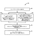
この点について、図6は、通信バス66が順序付けられたシーケンスにおいてアクティブである間、新たなデバイス識別情報を生成する図5中の通信バス66に結合されたスレーブデバイス62の例示的なプロセス100のフローチャートである。図6を参照すると、スレーブデバイス62は、通信バス66に結合された後に起動する(ブロック102)。たとえば、スレーブデバイス62は、電源がオンされた後に起動してもよい。スレーブデバイス62は、次いで、通信バス66と同期するために、通信バス66のバスアクティビティをリッスンし、同期ストリームを識別する(ブロック104)。たとえば、スレーブデバイス62は、通信バス66上のスレーブデバイスステータスレポートをリッスンしてもよい。また、スレーブデバイス62は、先に説明したように、そのデバイス識別情報(Device_Id)をプログラムまたは再プログラムするために、通信バス信号65から予想されるパターンをフィルタリングし、通信バス信号65の電気的特性を測定する(ブロック106)。たとえば、図5中のバス通信システム60(1)において、通信バス信号65は、通信バスクロック信号67である。したがって、スレーブデバイス62は、そのデバイス識別情報(Device_Id)をプログラムするために、図5の例では通信バスクロック信号67の電気的特性を測定する。
In this regard, FIG. 6 illustrates an
図6を引き続き参照すると、スレーブデバイス62が、バス通信の準備時間を短縮するために、並列動作でブロック104において通信バス66上のバスアクティビティをリッスンしながら、スレーブデバイス62は、ブロック106において、通信バス信号65から予測されるパターンをフィルタリングし、通信バス信号65の電気的特性を測定するように構成されてもよい。このようにして、スレーブデバイス62が通信バス66上で通信する準備ができているとき、スレーブデバイス62は、その新たなデバイス識別情報(Device_Id)を用いて通信バス66上でその存在を報告することができる(ブロック108)。スレーブデバイス62は、次いで、その新たにプログラムされたデバイス識別情報を使用して通信バス66上のバス通信に参加する(ブロック110)。
Continuing with FIG. 6, slave device 62 is in
スレーブデバイス62が通信バス信号65としてデータ信号の電気的特性を測定することによってそのデバイス識別情報をプログラムまたは再プログラムすることを可能にすることが望ましい場合もある。この点について、図7は、図5に提供するように通信バス66に結合されたスレーブデバイス62(1)〜62(N)とマスタデバイス64とを含む別の例示的なバス通信システム60(2)の概略図である。「N」は、スレーブデバイス62の数を表す。しかしながら、図7中のバス通信システム60(2)はまた、システムのプロトコルの一部として通信バスに結合されたスレーブデバイスのデバイス識別情報を呼び出す通信バスを含む任意の他のシステムであってもよい。デバイス識別情報生成回路48(1)〜48(N)は、それぞれ、通信バス66の共通データ線76に結合された外部プルアップまたはプルダウン抵抗器Rext(1)〜Rext(N)の結果として既存のデータピン80(1)〜80(N)に印加される可変電圧Vref(1)〜Vref(N)に基づいて、それらのそれぞれのスレーブデバイス62(1)〜62(N)のための新たなDevice_Idを生成するように構成される。可変電圧Vref(1)〜Vref(N)は、データ線76に適用される通信バスデータ信号78のトグリングの結果として生成され、データ線76は、データピン80(1)〜80(N)と、マスタデータピン82として設けられたマスタデータポートとに結合される。図5中のバス通信システム60(1)において設けられている通りに、通信バスデータ信号78のDC成分が、固有の可変電圧Vref(1)〜Vref(N)を生成するために外部抵抗器Rext(1)〜Rext(N)に適用されるように、AC結合74(1)〜74(N)は、通信バスデータ信号78の任意のAC成分をフィルタリングするために設けられ、データ線76に結合される。この点について、外部抵抗器Rext(1)〜Rext(N)は、固有のDevice_Idを生成するために、デバイス識別情報生成回路48(1)〜48(N)内のADCに異なるデジタル出力値を生成させるように可変電圧Vref(1)〜Vref(N)にさせる固有の抵抗値を有するように選択されることが可能である。
It may be desirable to allow the slave device 62 to program or reprogram its device identification information by measuring the electrical characteristics of the data signal as the communication bus signal 65. In this regard, FIG. 7 illustrates another exemplary bus communication system 60 (including slave devices 62 (1) -62 (N) and a
通信バス66がアクティブである間、新たなデバイス識別情報を生成するための、通信バス66に結合されたスレーブデバイス62の図6におけるプロセスはまた、図7中のバス通信システム60(2)内のスレーブデバイス62(1)〜62(N)によって用いられることが可能である。
The process in FIG. 6 of the slave device 62 coupled to the
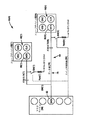
図8Aは、図7中のバス通信システム60(2)と同様の別の例示的なバス通信システム60(3)の概略図である。図8A中のバス通信システム60(3)では、スイッチSW(1)〜SW(N)は、外部抵抗器Rext(1)〜Rext(N)にVddまたはVss電力レールのいずれかを切替可能に結合するために、それぞれの外部抵抗器Rext(1)〜Rext(N)とVddまたはVssとの間に設けられ、配置される。スイッチSW(1)〜SW(N)は、マスタデバイス64によって、スレーブデバイス62(1)〜62(N)のDevice_Idを再プログラムすることが要求されたとき、外部抵抗器Rext(1)〜Rext(N)をVddまたはVssに結合するために閉じられるように、マスタデバイス64に結合されたスイッチ制御線84によって制御されることが可能である。同様に、マスタデバイス64がスレーブデバイス62(1)〜62(N)のDevice_Idを再プログラムした後、スイッチSW(1)〜SW(N)は、外部抵抗器Rext(1)〜Rext(N)をVddまたはVssに対して分離するために開かれるように、マスタデバイス64に結合されたスイッチ制御線84によって制御されることが可能である。このようにして、スレーブデバイス62(1)〜62(N)のDevice_Idがプログラムされていないとき、外部抵抗器Rext(1)〜Rext(N)は、電力が外部抵抗器Rext(1)〜Rext(N)によって消費されないように、VddまたはVssから分離され、それによって電力を節約する。
FIG. 8A is a schematic diagram of another exemplary bus communication system 60 (3) similar to the bus communication system 60 (2) in FIG. In the bus communication system 60 (3) in FIG. 8A, switches SW (1) to SW (N) can switch either Vdd or Vss power rails to external resistors Rext (1) to Rext (N). For coupling, each external resistor Rext (1) to Rext (N) is provided and arranged between Vdd or Vss. The switches SW (1) to SW (N) are connected to the external resistors Rext (1) to Rext when the
通信バス66がアクティブである間、新たなデバイス識別情報を生成するための、通信バス66に結合されたスレーブデバイス62の図6におけるプロセスはまた、図8A中のバス通信システム60(3)内のスレーブデバイス62(1)〜62(N)によって用いられることが可能である。
The process in FIG. 6 of the slave device 62 coupled to the
図8Bは、図8A中のバス通信システム60(3)と同様の別の例示的なバス通信システム60(4)の概略図である。しかしながら、スイッチSW(1)〜SW(N)は、外部抵抗器Rext(1)〜Rext(N)にVddまたはVss電力レールのいずれかを切替可能に結合するために、データピン80(1)〜80(N)とそれぞれの外部抵抗器Rext(1)〜Rext(N)との間に設けられ、配置される。スイッチSW(1)〜SW(N)は、初期化プロセスまたはスレーブデバイス62の発見プロセスの間などの、マスタデバイス64によって、スレーブデバイス62(1)〜62(N)のDevice_Idを再プログラムすることが要求されたとき、データピン80(1)〜80(N)をそれぞれの外部抵抗器Rext(1)〜Rext(N)に結合するために閉じられるように、マスタデバイス64に結合されたスイッチ制御線84によって制御されることが可能である。同様に、マスタデバイス64がスレーブデバイス62(1)〜62(N)のDevice_Idを再プログラムした後、スイッチSW(1)〜SW(N)は、データピン80(1)〜80(N)をそれぞれの外部抵抗器Rext(1)〜Rext(N)から分離するために開かれるように、マスタデバイス64に結合されたスイッチ制御線84によって制御されることが可能である。このようにして、スレーブデバイス62(1)〜62(N)のDevice_Idがプログラムされていないとき、外部抵抗器Rext(1)〜Rext(N)は、電力が外部抵抗器Rext(1)〜Rext(N)によって消費されないように、VddまたはVssから分離され、それによって電力を節約する。
FIG. 8B is a schematic diagram of another exemplary bus communication system 60 (4) similar to the bus communication system 60 (3) in FIG. 8A. However, switches SW (1) -SW (N) are connected to external resistors Rext (1) -Rext (N) to switchably couple either Vdd or Vss power rails to data pin 80 (1). ˜80 (N) and the respective external resistors Rext (1) ˜Rext (N). Switches SW (1) -SW (N) reprogram the Device_Id of slave devices 62 (1) -62 (N) by the
通信バス66がアクティブである間、新たなデバイス識別情報を生成するための、通信バス66に結合されたスレーブデバイス62の図6におけるプロセスはまた、図8B中のバス通信システム60(4)内のスレーブデバイス62(1)〜62(N)によって用いられることが可能である。
The process in FIG. 6 of the slave device 62 coupled to the
バス通信識別のためのデバイス識別情報の選択または再プログラムなどの外部制御を可能にするために電子デバイスにおけるデバイス識別情報生成を提供する例は、異なるタイプの通信バスを用いる異なる通信システムにおいて提供されることが可能である。他の通信システムはまた、固有のデバイス識別情報を有するために通信バスに通信可能に結合された電子デバイスを要求してもよい。 An example of providing device identification information generation in an electronic device to allow external control such as selection or reprogramming of device identification information for bus communication identification is provided in different communication systems using different types of communication buses. Is possible. Other communication systems may also require an electronic device communicatively coupled to the communication bus to have unique device identification information.
この点について、MIPI(登録商標)アライアンスは、オーディオチャネルに関するデジタルデータを電子デバイス内の異なるオーディオデバイスに転送するための通信プロトコルとして、SoundWireを最近発表した。本明細書で使用される場合、SoundWireの仕様は、その全体が参照により本明細書に組み込まれている、2014年10月29日に公開された、SOUNDWIRE specification version 8, revision 04を少なくとも意味することが意図される。Soundwireでは、1つのSoundWireマスタインターフェースは、マスタ電子デバイス(「マスタデバイス」)またはそれに通信可能に結合されたモニタが、SoundWireスレーブインターフェースに結合された1つまたは複数のスレーブ電子デバイス(「スレーブデバイス」)と、共通通信バスを介して通信することを可能にする。マスタデバイスは、2つの物理的信号、共通クロック線を介して通信されるクロック信号と、Soundwire通信バスの共通データ線を介して通信されるデータ信号とを使用して、スレーブデバイスと通信する。したがって、Soundwireシステムでは、データ衝突を回避するために、時分割多重(TDM)フレーム構造が、共通Soundwire通信バスを介するビットレートメディアストリームの搬送のために使用される。マスタデバイスは、バス通信のためにスレーブデバイスの各々に送信タイムスロットを割り当てる。したがって、Soundwireプロトコルは、Soundwire通信バスに接続されたスレーブデバイスの各々が、固有のデバイス識別情報を介してマスタデバイスによって確認されることを必要としてもよい。 In this regard, the MIPI® Alliance recently announced SoundWire as a communication protocol for transferring digital data about audio channels to different audio devices within an electronic device. As used herein, the SoundWire specification means at least the SOUNDWIRE specification version 8, revision 04 published October 29, 2014, which is hereby incorporated by reference in its entirety. Is intended. In Soundwire, a single SoundWire master interface is a master electronic device (a “master device”) or a monitor communicatively coupled to one or more slave electronic devices (a “slave device”) coupled to a SoundWire slave interface. ) And a common communication bus. The master device communicates with the slave device using two physical signals, a clock signal communicated via a common clock line, and a data signal communicated via a common data line of the Soundwire communication bus. Thus, in a Soundwire system, a time division multiplexing (TDM) frame structure is used for carrying bit rate media streams over a common Soundwire communication bus to avoid data collisions. The master device assigns a transmission time slot to each of the slave devices for bus communication. Accordingly, the Soundwire protocol may require that each slave device connected to the Soundwire communication bus be verified by the master device via unique device identification information.
この点について、図9は、例示的なSoundwireバス通信システム60(5)の概略図である。Soundwireバス通信システム60(5)は、Soundwire通信バス66Sに結合された例示的なSoundwireオーディオスレーブデバイス62S(1)〜62S(N)とSoundwireマスタデバイス64Sとを含み、ここで「N」は、Soundwireオーディオスレーブデバイス62S(1)〜62S(N)の数を表す。Soundwireマスタデバイス64Sおよび/またはSoundwireオーディオスレーブデバイス62S(1)〜62S(N)は、非限定的な例として、別々の構成要素内に設けられてもよく、または同じ回路基板上に配置されてもよい。Soundwireオーディオスレーブデバイス62S(1)〜62S(N)の各々は、図5中の上記で説明したデバイス識別情報生成回路48(1)〜48(N)と同様であることが可能なデバイス識別情報生成回路48S(1)〜48S(N)を有する。
In this regard, FIG. 9 is a schematic diagram of an exemplary Soundwire bus communication system 60 (5). Soundwire bus communication system 60 (5) includes exemplary Soundwire audio slave devices 62S (1) -62S (N) and
図9を引き続き参照すると、デバイス識別情報生成回路48S(1)〜48S(N)は、Soundwire通信バス信号65Sに適用される可変電圧Vref(1)〜Vref(N)に基づいて、それらのそれぞれのSoundwireオーディオスレーブデバイス62S(1)〜62S(N)のための新たなDevice_Id(図示せず)を生成するように構成される。この例では、Soundwireオーディオスレーブデバイス62S(1)〜62S(N)のための新たなDevice_Idを生成するために使用されるSoundwire通信バス信号65Sは、共通バスクロック信号67Sである。通信バスクロック信号67Sは、Soundwire通信バス66Sの共通クロック線70Sに結合された外部プルアップまたはプルダウン抵抗器Rext(1)〜Rext(N)の結果として、それぞれのSoundwireオーディオスレーブデバイス62S(1)〜62S(N)の既存のクロックピン68S(1)〜68S(N)上でアサートされる。可変電圧Vref(1)〜Vref(N)は、クロック線70Sに適用される通信バスクロック信号67Sの一定のトグリングレートの結果として生成され、クロック線70Sは、クロックピン68S(1)〜68S(N)と、マスタクロックピン72Sとして設けられたマスタクロックポートとに結合される。通信バスクロック信号67SのDC成分が、固有の可変電圧Vref(1)〜Vref(N)を生成するために外部抵抗器Rext(1)〜Rext(N)に適用されるように、AC結合74(1)〜74(N)は、通信バスクロック信号67SのAC成分をフィルタリングするために設けられ、クロック線70Sに結合される。この点について、外部抵抗器Rext(1)〜Rext(N)は、固有のデバイス識別情報(たとえば、Device_Id)を生成するために、デバイス識別情報生成回路48S(1)〜48S(N)内のADCに異なるデジタル出力値を生成させるように可変電圧Vref(1)〜Vref(N)にさせる固有の抵抗値を有するように選択されることが可能である。代替的には、別の例として、可変電圧Vref(1)〜Vref(N)は、外部抵抗器Rext(1)〜Rext(N)に適用されるSoundwire通信バス66Sの一部として制御信号(図示せず)をトグリングする結果として生成されることが可能である。
Still referring to FIG. 9, the device identification
Soundwire通信バス66Sが、Soundwireマスタデバイス64Sのマスタデータピン82Sからバス通信データを能動的にルーティングしながら、図9中のSoundwireバス通信システム60(5)内のSoundwireオーディオスレーブデバイス62S(1)〜62S(N)が、それらのそれぞれのデバイス識別情報をプログラムまたは再プログラムすることが可能であることが望ましい場合がある。このようにして、それらのデバイス識別情報をプログラムまたは再プログラムしていないSoundwireオーディオスレーブデバイス62S(1)〜62S(N)は、動作を続けることができる。たとえば、Soundwireオーディオスレーブデバイス62S(N)は、Soundwireオーディオスレーブデバイス62S(1)がSoundwire通信バス66Sにすでに結合され、Soundwire通信バス66Sを介してSoundwireマスタデバイス64SとのSoundwire通信データを能動的に受信および交換している後、Soundwire通信バス66Sに追加されてもよい。
While the
この点について、図10は、Soundwire通信バス66Sが順序付けられたシーケンスにおいてアクティブである間、新たなデバイス識別情報を生成する図9中のSoundwire通信バス66Sに結合されたSoundwireオーディオスレーブデバイス62Sの例示的なプロセス120のフローチャートである。図10を参照すると、Soundwireオーディオスレーブデバイス62Sは、Soundwire通信バス66Sに結合された後に起動する(ブロック122)。たとえば、Soundwireオーディオスレーブデバイス62Sは、電源がオンされた後に起動してもよい。Soundwireオーディオスレーブデバイス62Sは、次いで、Soundwire通信バス66Sと同期するために、Soundwire通信バス66Sのバスアクティビティをリッスンし、Soundwire同期ストリームを識別する(ブロック124)。たとえば、Soundwireオーディオスレーブデバイス62Sは、Soundwire通信バス66S上のSoundwireオーディオスレーブデバイスステータスレポートをリッスンしてもよい。また、Soundwireオーディオスレーブデバイス62Sは、先に説明したように、そのデバイス識別情報(Device_Id)をプログラムまたは再プログラムするために、Soundwire通信バス信号65Sから予想されるパターンをフィルタリングし、Soundwire通信バス信号65Sの電気的特性を測定する(ブロック126)。たとえば、図10中のSoundwireバス通信システム60(5)において、Soundwire通信バス信号65Sは、通信バスクロック信号67Sである。したがって、Soundwireオーディオスレーブデバイス62Sは、そのデバイス識別情報(Device_Id)をプログラムするために、図9の例では通信バスクロック信号67Sの電気的特性を測定する。
In this regard, FIG. 10 illustrates an example of a Soundwire audio slave device 62S coupled to the
図10を引き続き参照すると、Soundwireオーディオスレーブデバイス62Sが、バス通信の準備時間を短縮するために、並列動作でブロック114においてSoundwire通信バス66S上のバスアクティビティをリッスンしながら、Soundwireオーディオスレーブデバイス62Sは、ブロック116において、Soundwire通信バス信号65Sから予測されるパターンをフィルタリングし、Soundwire通信バス信号65Sの電気的特性を測定するように構成されてもよい。このようにして、Soundwireオーディオスレーブデバイス62SがSoundwire通信バス66S上で通信する準備ができているとき、Soundwireオーディオスレーブデバイス62Sは、その新たなデバイス識別情報(Device_Id)を用いてSoundwire通信バス66S上でその存在を報告することができる(ブロック128)。Soundwireオーディオスレーブデバイス62Sは、次いで、その新たにプログラムされたデバイス識別情報を使用してSoundwire通信バス66S上のバス通信に参加する(ブロック130)。
Continuing to refer to FIG. 10, the Soundwire audio slave device 62S is listening for bus activity on the
バス通信識別のためのデバイス識別情報の選択または再プログラムなどの外部制御を可能にするために本明細書で開示されたデバイス識別情報生成回路を含むオーディオ電子デバイスは、任意のプロセッサベースのデバイス内に設けられてもよく、またはそこに組み込まれてもよい。例は、限定はしないが、セットトップボックス、娯楽ユニット、ナビゲーションデバイス、通信デバイス、固定位置データユニット、モバイル位置データユニット、携帯電話、セルラー電話、コンピュータ、ポータブルコンピュータ、デスクトップコンピュータ、携帯情報端末(PDA)、モニタ、コンピュータモニタ、テレビジョン、チューナ、ラジオ、衛星ラジオ、音楽プレーヤ、デジタル音楽プレーヤ、ポータブル音楽プレーヤ、デジタルビデオプレーヤ、ビデオプレーヤ、デジタルビデオディスク(DVD)プレーヤ、およびポータブルデジタルビデオプレーヤを含む。 An audio electronic device that includes a device identification information generation circuit disclosed herein to enable external control such as selection or reprogramming of device identification information for bus communication identification is provided within any processor-based device. Or may be incorporated therein. Examples include, but are not limited to, set-top boxes, entertainment units, navigation devices, communication devices, fixed location data units, mobile location data units, mobile phones, cellular phones, computers, portable computers, desktop computers, personal digital assistants (PDAs) ), Monitor, computer monitor, television, tuner, radio, satellite radio, music player, digital music player, portable music player, digital video player, video player, digital video disc (DVD) player, and portable digital video player .
当業者は、本明細書に開示された態様に関連して説明した様々な例示的な論理ブロック、モジュール、回路、およびアルゴリズムが、電子ハードウェア、メモリもしくは別のコンピュータ可読媒体内に記憶され、プロセッサもしくは他の処理デバイスによって実行される命令、または両方の組合せとして実施されてもよいことをさらに理解するであろう。本明細書で説明されるマスタデバイスおよびスレーブデバイスは、例として、任意の回路、ハードウェア構成要素、集積回路(IC)、またはICチップとして実施され得る。本明細書で開示されるメモリは、任意のタイプおよびサイズのメモリであり得、任意のタイプの所望の情報を記憶するように構成され得る。この互換性を明確に示すために、様々な例示的構成要素、ブロック、モジュール、回路、およびステップが、その機能に関して一般的に上記で説明された。そのような機能がどのように実装されるかは、特定の応用分野、設計の選択、および/またはシステム全体に対して課される設計制約に依存する。当業者は、説明される機能を各々の特定の応用分野について様々な方式で実装し得るが、そのような実装判断が、本開示の範囲からの逸脱を引き起こすと解釈されるべきではない。 Those of ordinary skill in the art may store various exemplary logic blocks, modules, circuits, and algorithms described in connection with aspects disclosed herein in electronic hardware, memory, or other computer-readable media, It will be further understood that the instructions may be implemented as instructions executed by a processor or other processing device, or a combination of both. The master and slave devices described herein may be implemented as any circuit, hardware component, integrated circuit (IC), or IC chip, by way of example. The memory disclosed herein may be any type and size of memory and may be configured to store any type of desired information. To clearly illustrate this compatibility, various exemplary components, blocks, modules, circuits, and steps have been described above generally in terms of their functionality. How such functionality is implemented depends on the particular application area, design choices, and / or design constraints imposed on the overall system. Those skilled in the art may implement the described functionality in a variety of ways for each particular application, but such implementation decisions should not be construed as causing a departure from the scope of the present disclosure.
本明細書で開示された態様に関連して説明した様々な例示的な論理ブロック、モジュール、および回路は、プロセッサ、デジタル信号プロセッサ(DSP)、特定用途向け集積回路(ASIC)、フィールドプログラマブルゲートアレイ(FPGA)もしくは他のプログラマブル論理デバイス、ディスクリートゲートもしくはトランジスタロジック、ディスクリートハードウェア構成要素、または、本明細書に記載の機能を実行するように設計されたそれらの任意の組合せで実施または実行されてもよい。プロセッサはマイクロプロセッサであり得るが、代替実施形態では、プロセッサは、任意の従来型プロセッサ、コントローラ、マイクロコントローラ、または状態機械であり得る。プロセッサはまた、コンピューティングデバイスの組合せ、たとえばDSPとマイクロプロセッサの組合せ、複数のマイクロプロセッサ、1つまたは複数のマイクロプロセッサとDSPコア、または任意の他のそのような構成として実装され得る。 The various exemplary logic blocks, modules, and circuits described in connection with the aspects disclosed herein are processors, digital signal processors (DSPs), application specific integrated circuits (ASICs), field programmable gate arrays. (FPGA) or other programmable logic device, discrete gate or transistor logic, discrete hardware components, or any combination thereof designed to perform the functions described herein Also good. The processor can be a microprocessor, but in alternative embodiments the processor can be any conventional processor, controller, microcontroller, or state machine. The processor may also be implemented as a combination of computing devices, such as a combination of DSP and microprocessor, multiple microprocessors, one or more microprocessors and DSP cores, or any other such configuration.
本明細書で開示された態様は、ハードウェアおよびハードウェア内に記憶された命令において具体化されてもよく、たとえば、ランダムアクセスメモリ(RAM)、フラッシュメモリ、読出し専用メモリ(ROM)、電気的プログラマブルROM(EPROM)、電気的消去可能プログラマブルROM(EEPROM)、レジスタ、ハードディスク、リムーバブルディスク、CD-ROM、または当該技術分野において公知の任意の他の形態のコンピュータ可読媒体内に存在してもよい。例示的記憶媒体は、プロセッサが記憶媒体から情報を読み取り、記憶媒体に情報を書き込み得るようにプロセッサに結合される。代替実施形態では、記憶媒体はプロセッサと一体であり得る。プロセッサおよび記憶媒体は、ASIC内にあり得る。ASICはリモート局内にあり得る。代替実施形態では、プロセッサおよび記憶媒体は、別個の構成要素としてリモート局、基地局、またはサーバ内にあり得る。 Aspects disclosed herein may be embodied in hardware and instructions stored in hardware, such as random access memory (RAM), flash memory, read only memory (ROM), electrical It may reside in a programmable ROM (EPROM), an electrically erasable programmable ROM (EEPROM), a register, a hard disk, a removable disk, a CD-ROM, or any other form of computer readable medium known in the art . An exemplary storage medium is coupled to the processor such that the processor can read information from, and write information to, the storage medium. In an alternative embodiment, the storage medium may be integral to the processor. The processor and the storage medium can be in an ASIC. The ASIC can be in a remote station. In alternative embodiments, the processor and the storage medium may be in a remote station, base station, or server as separate components.
また、本明細書における例示的な態様のいずれかにおいて説明した動作ステップは、例および説明を提供するために説明されていることに留意されたい。説明される動作は、図示されるシーケンス以外の多数の異なるシーケンスで実施され得る。さらに、単一の動作ステップで説明される動作は、実際にはいくつかの異なるステップで実施され得る。さらに、例示的態様で論じられる1つまたは複数の動作ステップが組み合わされ得る。フローチャート図内に示す動作ステップは、当業者に容易に明らかになるように、多数の異なる変更を受けてもよいことが理解されるべきである。当業者はまた、情報および信号が様々な異なる技術および技法のいずれかを使用して表されてもよいことを理解するであろう。たとえば、上記の説明全体にわたって参照される場合があるデータ、命令、コマンド、情報、信号、ビット、シンボル、およびチップは、電圧、電流、電磁波、磁場もしくは磁性粒子、光場もしくは光学粒子、またはそれらの任意の組合せによって表すことができる。 It should also be noted that the operational steps described in any of the exemplary aspects herein are described to provide examples and explanations. The described operations may be performed in a number of different sequences other than the illustrated sequence. Furthermore, the operations described in a single operation step may actually be performed in several different steps. Further, one or more operational steps discussed in the exemplary aspects may be combined. It should be understood that the operational steps shown in the flowchart diagrams may be subject to a number of different modifications, as will be readily apparent to those skilled in the art. Those skilled in the art will also understand that information and signals may be represented using any of a variety of different technologies and techniques. For example, data, instructions, commands, information, signals, bits, symbols, and chips that may be referred to throughout the above description are voltages, currents, electromagnetic waves, magnetic or magnetic particles, optical or optical particles, or Can be represented by any combination of
本開示の前述の説明は、当業者が本開示を製造または使用することを可能にするために提供される。本開示に対する種々の変更形態が、当業者から見て容易に明らかとなり、本明細書において規定される一般原理は、本開示の趣旨または範囲から逸脱することなく、他の変形形態に適用することができる。したがって、本開示は、本明細書において説明される例および設計に限定されるものではなく、本明細書において開示される原理および新規の特徴に合致する最も広い範囲を与えられるべきである。 The previous description of the disclosure is provided to enable any person skilled in the art to make or use the disclosure. Various modifications to the present disclosure will be readily apparent to those skilled in the art, and the general principles defined herein may be applied to other variations without departing from the spirit or scope of the present disclosure. Can do. Accordingly, the present disclosure is not intended to be limited to the examples and designs described herein, but is to be accorded the widest scope consistent with the principles and novel features disclosed herein.
30 電子デバイス
30(1) 電子デバイス
30(2) 電子デバイス
30(3) 電子デバイス
30(4) 電子デバイス
32 外部ピン
34 電源ピン
36 接地ピン
38 データピン
40 クロックピン
42 会議ピン
44 内部デバイス識別情報メモリ、Device_Id
44(1) Device_Id
44(2) Device_Id
44(3) Device_Id
44(4) Device_Id
44(5) Device_Id
46 外部ピン
48 デバイス識別情報生成回路
48(1)〜48(N) デバイス識別情報生成回路
48(2) デバイス識別情報生成回路
48(3) デバイス識別情報生成回路
48S(1)〜48S(N) デバイス識別情報生成回路
50 外部ソース
50(1) 外部可変電圧源
50(2) 外部ソース
50(3) 外部ソース
50(4) 外部ソース
52 回路
52(1) 回路
52(2) 回路
52(3) 回路
52(4) 回路
54 アナログ-デジタル変換器、ADC
55 デバイス識別情報選択回路
56 外部抵抗器
56(1) 外部可変抵抗器
57 バッファ回路
58(1) 外部可変キャパシタ
59 表
60(1) バス通信システム
60(2) バス通信システム
60(3) バス通信システム
60(4) バス通信システム
60(5) Soundwireバス通信システム
61 デコーダ線
62 スレーブデバイス
62(1)〜62(N) スレーブデバイス
62S(1)〜62S(N) Soundwireオーディオスレーブデバイス
63 デコーダ
64 マスタデバイス
64S Soundwireマスタデバイス
65 通信バス信号
65S Soundwire通信バス信号
66 通信バス
66S Soundwire通信バス
67 通信バスクロック信号
67S 通信バスクロック信号
68(1)〜68(N) クロックピン
68S(1)〜68S(N) クロックピン
70 共通クロック線
70S クロック線
72 マスタクロックピン
72S マスタクロックピン
74(1)〜74(N) AC結合
76 共通データ線
78 通信バスデータ信号
80(1)〜80(N) データピン
82 マスタデータピン
82S マスタデータピン
84 スイッチ制御線
30 electronic devices
30 (1) Electronic devices
30 (2) Electronic devices
30 (3) Electronic devices
30 (4) Electronic devices
32 External pin
34 Power pin
36 Ground pin
38 Data pin
40 clock pins
42 Conference pin
44 Internal device identification information memory, Device_Id
44 (1) Device_Id
44 (2) Device_Id
44 (3) Device_Id
44 (4) Device_Id
44 (5) Device_Id
46 External pin
48 Device identification information generation circuit
48 (1) to 48 (N) Device identification information generation circuit
48 (2) Device identification information generation circuit
48 (3) Device identification information generation circuit
48S (1) to 48S (N) Device identification information generation circuit
50 External source
50 (1) External variable voltage source
50 (2) External source
50 (3) External source
50 (4) External source
52 circuits
52 (1) Circuit
52 (2) Circuit
52 (3) Circuit
52 (4) Circuit
54 Analog-to-digital converter, ADC
55 Device identification information selection circuit
56 External resistor
56 (1) External variable resistor
57 Buffer circuit
58 (1) External variable capacitor
59 Table
60 (1) Bus communication system
60 (2) Bus communication system
60 (3) Bus communication system
60 (4) Bus communication system
60 (5) Soundwire bus communication system
61 Decoder line
62 Slave device
62 (1) to 62 (N) Slave device
62S (1) -62S (N) Soundwire audio slave device
63 Decoder
64 Master device
64S Soundwire master device
65 Communication bus signal
65S Soundwire communication bus signal
66 Communication bus
66S Soundwire communication bus
67 Communication bus clock signal
67S communication bus clock signal
68 (1) to 68 (N) Clock pin
68S (1) to 68S (N) Clock pin
70 Common clock line
70S clock line
72 Master clock pin
72S Master clock pin
74 (1) to 74 (N) AC coupling
76 Common data line
78 Communication bus data signal
80 (1) ~ 80 (N) Data pin
82 Master data pin
82S Master data pin
84 Switch control line
Claims (36)
通信バスに結合されるように構成されたデバイス識別ポートと、
前記デバイス識別ポートに結合されたデバイス識別情報生成回路とを備え、
前記デバイス識別情報生成回路が、
前記デバイス識別ポート上で前記通信バスから受信した通信バス信号の電気的特性を検出し、
前記検出された電気的特性に基づいてデバイス識別情報を生成し、
前記生成されたデバイス識別情報をデバイス識別情報メモリ内に記憶するように構成された、電子デバイス。 An electronic device configured to reprogram the device identification information,
A device identification port configured to be coupled to the communication bus;
A device identification information generation circuit coupled to the device identification port;
The device identification information generating circuit is
Detecting electrical characteristics of a communication bus signal received from the communication bus on the device identification port;
Generating device identification information based on the detected electrical characteristics;
An electronic device configured to store the generated device identification information in a device identification information memory.
前記デバイス識別情報生成回路が、前記デバイス識別ポート上で前記通信バスから受信した通信バスクロック信号から構成された前記通信バス信号の前記電気的特性を検出するように構成された、請求項1に記載の電子デバイス。 The device identification port is configured to be coupled to a clock line of the communication bus;
The device identification information generation circuit is configured to detect the electrical characteristic of the communication bus signal configured from a communication bus clock signal received from the communication bus on the device identification port. The electronic device described.
前記デバイス識別情報生成回路が、前記デバイス識別ポート上で前記通信バスから受信した通信バスデータ信号から構成された前記通信バス信号の前記電気的特性を検出するように構成された、請求項1に記載の電子デバイス。 The device identification port is configured to be coupled to a data line of the communication bus;
The device identification information generation circuit is configured to detect the electrical characteristic of the communication bus signal configured from a communication bus data signal received from the communication bus on the device identification port. The electronic device described.
前記デバイス識別情報生成回路が、前記検出された電気的特性に基づいて、前記デバイス識別情報の前記複数のデバイス識別子のうちの少なくとも1つのデバイス識別子を選択するように構成されたデバイス識別情報選択回路を備える、請求項1に記載の電子デバイス。 The device identification information comprises a plurality of device identifiers;
The device identification information selection circuit configured to select at least one device identifier of the plurality of device identifiers of the device identification information based on the detected electrical characteristic. The electronic device according to claim 1, comprising:
前記デバイス識別情報生成回路が、前記同期ストリームの識別の間に、前記デバイス識別ポート上で前記通信バスから受信した前記通信バス信号の前記電気的特性を検出するように構成された、請求項1に記載の電子デバイス。 Configured to identify a synchronization stream for synchronizing the electronic device to the communication bus;
The device identification information generation circuit is configured to detect the electrical characteristic of the communication bus signal received from the communication bus on the device identification port during identification of the synchronization stream. The electronic device according to.
通信バスに結合するために構成されたデバイス識別手段と、
前記デバイス識別手段に結合されたデバイス識別情報生成手段とを備え、
前記デバイス識別情報生成手段が、
前記デバイス識別手段上で前記通信バスから受信した通信バス信号の電気的特性を検出し、
前記検出された電気的特性に基づいてデバイス識別情報を生成し、
前記生成されたデバイス識別情報をデバイス識別情報メモリ内に記憶するためのものである、電子デバイス。 An electronic device configured to reprogram the device identification information,
Device identification means configured for coupling to a communication bus;
Device identification information generating means coupled to the device identification means,
The device identification information generating means is
Detecting electrical characteristics of a communication bus signal received from the communication bus on the device identification means;
Generating device identification information based on the detected electrical characteristics;
An electronic device for storing the generated device identification information in a device identification information memory.
通信バスに結合されたデバイス識別ポート上で前記通信バスから受信した通信バス信号の電気的特性を検出するステップと、
前記通信バス信号の前記検出された電気的特性に基づいてデバイス識別情報を生成するステップと、
前記生成されたデバイス識別情報をデバイス識別情報メモリ内に記憶するステップと
を備える方法。 A method for an electronic device to reprogram its device identification information, comprising:
Detecting electrical characteristics of a communication bus signal received from the communication bus on a device identification port coupled to the communication bus;
Generating device identification information based on the detected electrical characteristics of the communication bus signal;
Storing the generated device identification information in a device identification information memory.
前記通信バス信号の前記電気的特性を検出するステップが、前記同期ストリームを識別するステップの間に実行される、請求項23に記載の方法。 Further comprising identifying a synchronization stream to synchronize the electronic device with the communication bus;
24. The method of claim 23, wherein detecting the electrical characteristic of the communication bus signal is performed during the step of identifying the synchronization stream.
データ線とクロック線とから構成された通信バスと、
マスタデータポートとマスタクロックポートとから構成されたマスタデバイスであって、前記マスタデバイスが、前記データ線に結合された前記マスタデータポートと前記クロック線に結合された前記マスタクロックポートとによって前記通信バスに結合された、マスタデバイスと、
複数のスレーブデバイスとを備え、前記複数のスレーブデバイスの各々が、
前記通信バスに結合されたデータポートおよびクロックポートであって、前記データポートおよび前記クロックポートのうちの少なくとも1つがデバイス識別ポートも備え、
前記データポートが前記通信バスの前記データ線に結合され、前記クロックポートが前記通信バスの前記クロック線に結合された、データポートおよびクロックポートと、
前記デバイス識別ポートに結合されたデバイス識別情報生成回路とを備え、前記デバイス識別情報生成回路が、
前記デバイス識別ポート上で前記通信バスから受信した通信バス信号の電気的特性を検出し、
前記検出された電気的特性に基づいてデバイス識別情報を生成し、
前記生成されたデバイス識別情報をデバイス識別情報メモリ内に記憶するように構成された、バス通信システム。 A bus communication system for allowing a slave device coupled to a communication bus to reprogram its device identification information,
A communication bus composed of a data line and a clock line;
A master device comprising a master data port and a master clock port, wherein the master device communicates with the master data port coupled to the data line and the master clock port coupled to the clock line. A master device coupled to the bus;
A plurality of slave devices, each of the plurality of slave devices,
A data port and a clock port coupled to the communication bus, wherein at least one of the data port and the clock port also includes a device identification port;
A data port and a clock port, wherein the data port is coupled to the data line of the communication bus, and the clock port is coupled to the clock line of the communication bus;
A device identification information generation circuit coupled to the device identification port, the device identification information generation circuit,
Detecting electrical characteristics of a communication bus signal received from the communication bus on the device identification port;
Generating device identification information based on the detected electrical characteristics;
A bus communication system configured to store the generated device identification information in a device identification information memory.
複数の外部抵抗器であって、前記複数の外部抵抗器のうちの外部抵抗器が前記複数のスレーブデバイスの各々の前記デバイス識別ポートに結合された、複数の外部抵抗器と
をさらに備える、請求項29に記載のバス通信システム。 A plurality of AC couplings, wherein a plurality of AC couplings are coupled to the device identification port of each of the plurality of slave devices;
A plurality of external resistors, wherein the external resistors of the plurality of external resistors are further coupled to the device identification port of each of the plurality of slave devices. Item 30 is a bus communication system.
前記複数のスイッチの各々の開閉を制御するように構成されたスイッチ制御線と
をさらに備え、
前記マスタデバイスが、前記複数のスレーブデバイスの各々に関して前記複数の外部抵抗器のうちの前記外部抵抗器のデバイス識別ポートへの結合を制御するために前記複数のスイッチの各々を開かせるまたは閉じさせるために前記スイッチ制御線上に制御信号を生成するように構成された、請求項30に記載のバス通信システム。 A plurality of switches, wherein a switch of the plurality of switches is configured to switchably couple the external resistor to the device identification port of the slave device for each of the plurality of slave devices. A switch,
A switch control line configured to control opening and closing of each of the plurality of switches,
The master device causes each of the plurality of switches to open or close to control coupling of the external resistor to the device identification port of the plurality of external resistors for each of the plurality of slave devices. 32. The bus communication system according to claim 30, configured to generate a control signal on the switch control line for the purpose.
前記デバイス識別情報生成回路が、前記同期ストリームの識別の間に、前記デバイス識別ポート上で前記通信バスから受信した前記通信バス信号の前記電気的特性を検出するように構成された、請求項29に記載のバス通信システム。 Configured to identify a synchronization stream for synchronizing the slave device to the communication bus;
30. The device identification information generation circuit is configured to detect the electrical characteristic of the communication bus signal received from the communication bus on the device identification port during identification of the synchronization stream. A bus communication system according to claim 1.
前記デバイス識別情報生成回路が、前記デバイス識別ポート上で前記Soundwire通信バスから受信したSoundwire通信バス信号から構成され前記通信バス信号の前記電気的特性を検出するように構成された、請求項35に記載のバス通信システム。 The communication bus is composed of a Soundwire communication bus,
The device identification information generation circuit is configured to detect the electrical characteristic of the communication bus signal configured from a Soundwire communication bus signal received from the Soundwire communication bus on the device identification port. The bus communication system described.
Applications Claiming Priority (7)
| Application Number | Priority Date | Filing Date | Title |
|---|---|---|---|
| US201461935115P | 2014-02-03 | 2014-02-03 | |
| US201461935134P | 2014-02-03 | 2014-02-03 | |
| US61/935,115 | 2014-02-03 | ||
| US61/935,134 | 2014-02-03 | ||
| US14/609,488 | 2015-01-30 | ||
| US14/609,488 US10114787B2 (en) | 2014-02-03 | 2015-01-30 | Device identification generation in electronic devices to allow external control of device identification for bus communications identification, and related systems and methods |
| PCT/US2015/014067 WO2015117061A1 (en) | 2014-02-03 | 2015-02-02 | Device identification generation in electronic devices to allow external control of device identification for bus communications identification, and related systems and methods |
Publications (2)
| Publication Number | Publication Date |
|---|---|
| JP2017505067A true JP2017505067A (en) | 2017-02-09 |
| JP2017505067A5 JP2017505067A5 (en) | 2018-03-01 |
Family
ID=53754948
Family Applications (1)
| Application Number | Title | Priority Date | Filing Date |
|---|---|---|---|
| JP2016549086A Pending JP2017505067A (en) | 2014-02-03 | 2015-02-02 | Generation of device identification information in an electronic device enabling external control of device identification information for bus communication identification, and related systems and methods |
Country Status (7)
| Country | Link |
|---|---|
| US (1) | US10114787B2 (en) |
| EP (1) | EP3103247A1 (en) |
| JP (1) | JP2017505067A (en) |
| KR (1) | KR20160118269A (en) |
| CN (1) | CN105940661A (en) |
| CA (1) | CA2935766A1 (en) |
| WO (1) | WO2015117061A1 (en) |
Cited By (2)
| Publication number | Priority date | Publication date | Assignee | Title |
|---|---|---|---|---|
| JP2018182673A (en) * | 2017-04-21 | 2018-11-15 | 株式会社デンソー | Assembly, main body device and attachment device |
| JP2019096740A (en) * | 2017-11-22 | 2019-06-20 | 富士通株式会社 | Electronic device |
Families Citing this family (9)
| Publication number | Priority date | Publication date | Assignee | Title |
|---|---|---|---|---|
| KR20150125433A (en) * | 2014-04-30 | 2015-11-09 | 삼성전자주식회사 | Method and apparatus for generating identifier of slave device |
| US10387352B2 (en) * | 2015-06-05 | 2019-08-20 | Kulite Semiconductor Products, Inc. | Systems and methods for multibit code communications |
| US20170063700A1 (en) * | 2015-08-26 | 2017-03-02 | Qualcomm Incorporated | Systems and methods for rate detection for soundwire extension (soundwire-xl) cables |
| DE112017005458T5 (en) * | 2016-10-28 | 2019-07-25 | Knowles Electronics, Llc | TRANSFORMER ARRANGEMENTS AND METHOD |
| US10511397B2 (en) | 2018-01-24 | 2019-12-17 | Qualcomm Incorporated | Virtual general purpose input/output (GPIO) (VGI) over a time division multiplex (TDM) bus |
| CN110880998B (en) * | 2019-12-03 | 2022-09-20 | 锐捷网络股份有限公司 | Message transmission method and device based on programmable device |
| US11934285B2 (en) * | 2021-01-15 | 2024-03-19 | Google Llc | Identification/communication interface between consumer electronic devices and accessory devices |
| CN114285692B (en) * | 2021-12-22 | 2023-09-01 | 广州极飞科技股份有限公司 | Communication control system, identity determination method, distribution method and equipment |
| CN115361432B (en) * | 2022-08-31 | 2023-05-09 | 小米汽车科技有限公司 | Communication control method and device between master and slave devices, vehicle and storage medium |
Citations (6)
| Publication number | Priority date | Publication date | Assignee | Title |
|---|---|---|---|---|
| JPH0537535A (en) * | 1991-08-02 | 1993-02-12 | Nec Corp | Address control circuit |
| JPH09284312A (en) * | 1996-04-09 | 1997-10-31 | Nippon Signal Co Ltd:The | Bus system |
| JPH11214166A (en) * | 1998-01-27 | 1999-08-06 | Matsushita Electric Works Ltd | Lighting system |
| JP2000315128A (en) * | 1999-04-30 | 2000-11-14 | Mitsubishi Electric Corp | Bus control system |
| JP2009118155A (en) * | 2007-11-06 | 2009-05-28 | Kyocera Mita Corp | Slave node, image forming apparatus, and method of setting slave address |
| JP2011155356A (en) * | 2010-01-26 | 2011-08-11 | Denso Corp | Communication slave and communication network system |
Family Cites Families (25)
| Publication number | Priority date | Publication date | Assignee | Title |
|---|---|---|---|---|
| US5276442A (en) * | 1991-02-22 | 1994-01-04 | Ericsson Ge Mobile Communications Inc. | Dynamic address allocation within RF trunking multisite switch |
| US6246696B1 (en) * | 1995-09-11 | 2001-06-12 | Kabushiki Kaisha Toshiba | Method of controlling a communication and apparatus for the same |
| JPH11177593A (en) * | 1997-12-08 | 1999-07-02 | Yazaki Corp | Address setting method and communication system to which the method is applied |
| US6629172B1 (en) | 1998-12-14 | 2003-09-30 | Micron Technology, Inc. | Multi-chip addressing for the I2C bus |
| US6820148B1 (en) * | 2000-08-17 | 2004-11-16 | Sandisk Corporation | Multiple removable non-volatile memory cards serially communicating with a host |
| US8335868B2 (en) * | 2006-03-28 | 2012-12-18 | Mosaid Technologies Incorporated | Apparatus and method for establishing device identifiers for serially interconnected devices |
| US7587539B2 (en) | 2006-04-25 | 2009-09-08 | Texas Instruments Incorporated | Methods of inter-integrated circuit addressing and devices for performing the same |
| US8984249B2 (en) * | 2006-12-20 | 2015-03-17 | Novachips Canada Inc. | ID generation apparatus and method for serially interconnected devices |
| US7827330B2 (en) | 2007-07-27 | 2010-11-02 | Microchip Technology Incorporated | Configuring multi-bit slave addressing on a serial bus using a single external connection |
| US7893699B2 (en) | 2007-12-03 | 2011-02-22 | Infineon Technologies Ag | Method for identifying electronic circuits and identification device |
| CN101727099A (en) | 2008-10-27 | 2010-06-09 | 上海工程技术大学 | Identification and information exchange platform based on I2C structural model and communication protocol unit |
| US8225021B2 (en) | 2009-05-28 | 2012-07-17 | Lexmark International, Inc. | Dynamic address change for slave devices on a shared bus |
| US8205017B2 (en) | 2009-11-17 | 2012-06-19 | Aptina Imaging Corporation | Systems and methods for addressing and synchronizing multiple devices |
| DE102010005104B3 (en) | 2010-01-20 | 2011-07-21 | Texas Instruments Deutschland GmbH, 85356 | Electronic device and method for a larger address range on an IIC or an IIC compatible bus |
| CN102147782B (en) | 2010-02-08 | 2013-08-21 | 鸿富锦精密工业(深圳)有限公司 | Communication circuit between master equipment and slave equipment and ID (Identity) address allocating method thereof |
| US8825908B2 (en) | 2010-06-15 | 2014-09-02 | Intel Mobile Communications GmbH | Method of identifying devices on a bus and apparatus |
| US8478917B2 (en) | 2010-09-22 | 2013-07-02 | Microsoft Corporation | Automatic addressing protocol for a shared bus |
| US9454504B2 (en) | 2010-09-30 | 2016-09-27 | Hewlett-Packard Development Company, L.P. | Slave device bit sequence zero driver |
| CN102567250B (en) | 2010-11-29 | 2016-06-01 | 意法半导体股份有限公司 | There is the electronic equipment of the address of the terminal programming that can pass through to reduce quantity |
| US9003096B2 (en) | 2011-03-16 | 2015-04-07 | Texas Instruments Incorporated | Serial interface |
| US20120303836A1 (en) | 2011-05-23 | 2012-11-29 | Rf Micro Devices, Inc. | Slave id configuration |
| US9037766B2 (en) * | 2011-11-18 | 2015-05-19 | Fairchild Semiconductor Corporation | Pin selectable I2C slave addresses |
| US20130257667A1 (en) | 2012-03-30 | 2013-10-03 | Broadcom Corporation | Antenna Tuning |
| CN102724110B (en) | 2012-05-25 | 2016-03-09 | 华为技术有限公司 | The veneer means of communication, system and veneer |
| CN104981790B (en) * | 2013-02-22 | 2017-12-01 | 马维尔国际贸易有限公司 | Multiple-grooved multi-point audio interface |
-
2015
- 2015-01-30 US US14/609,488 patent/US10114787B2/en active Active
- 2015-02-02 JP JP2016549086A patent/JP2017505067A/en active Pending
- 2015-02-02 EP EP15711594.0A patent/EP3103247A1/en not_active Withdrawn
- 2015-02-02 WO PCT/US2015/014067 patent/WO2015117061A1/en active Application Filing
- 2015-02-02 CA CA2935766A patent/CA2935766A1/en not_active Abandoned
- 2015-02-02 KR KR1020167021650A patent/KR20160118269A/en not_active Application Discontinuation
- 2015-02-02 CN CN201580006798.3A patent/CN105940661A/en active Pending
Patent Citations (6)
| Publication number | Priority date | Publication date | Assignee | Title |
|---|---|---|---|---|
| JPH0537535A (en) * | 1991-08-02 | 1993-02-12 | Nec Corp | Address control circuit |
| JPH09284312A (en) * | 1996-04-09 | 1997-10-31 | Nippon Signal Co Ltd:The | Bus system |
| JPH11214166A (en) * | 1998-01-27 | 1999-08-06 | Matsushita Electric Works Ltd | Lighting system |
| JP2000315128A (en) * | 1999-04-30 | 2000-11-14 | Mitsubishi Electric Corp | Bus control system |
| JP2009118155A (en) * | 2007-11-06 | 2009-05-28 | Kyocera Mita Corp | Slave node, image forming apparatus, and method of setting slave address |
| JP2011155356A (en) * | 2010-01-26 | 2011-08-11 | Denso Corp | Communication slave and communication network system |
Cited By (3)
| Publication number | Priority date | Publication date | Assignee | Title |
|---|---|---|---|---|
| JP2018182673A (en) * | 2017-04-21 | 2018-11-15 | 株式会社デンソー | Assembly, main body device and attachment device |
| JP2019096740A (en) * | 2017-11-22 | 2019-06-20 | 富士通株式会社 | Electronic device |
| JP7059585B2 (en) | 2017-11-22 | 2022-04-26 | 富士通株式会社 | Electronic device |
Also Published As
| Publication number | Publication date |
|---|---|
| US10114787B2 (en) | 2018-10-30 |
| EP3103247A1 (en) | 2016-12-14 |
| US20150220475A1 (en) | 2015-08-06 |
| CN105940661A (en) | 2016-09-14 |
| KR20160118269A (en) | 2016-10-11 |
| WO2015117061A1 (en) | 2015-08-06 |
| CA2935766A1 (en) | 2015-08-06 |
Similar Documents
| Publication | Publication Date | Title |
|---|---|---|
| JP2017505067A (en) | Generation of device identification information in an electronic device enabling external control of device identification information for bus communication identification, and related systems and methods | |
| JP6013596B2 (en) | Multi-format digital audio interface | |
| EP3216172B1 (en) | Predefined static enumeration for dynamic enumeration buses | |
| KR102423168B1 (en) | Multiplexing distinct signals on a single pin of a memory device | |
| CN110119372B (en) | Selective control of on-die termination in a multi-column system | |
| US9252900B2 (en) | Universal synchronization engine based on probabilistic methods for guarantee of lock in multiformat audio systems | |
| KR102300933B1 (en) | Memory system that supports dual-mode modulation | |
| KR20200037885A (en) | Multiple simultaneous modulation schemes in memory systems | |
| US20170063700A1 (en) | Systems and methods for rate detection for soundwire extension (soundwire-xl) cables | |
| US9326079B2 (en) | Detection circuit | |
| WO2016094052A1 (en) | Adjustable low swing memory interface | |
| US20140149616A1 (en) | I2c bus structure and address management method | |
| US9667254B2 (en) | Electronic device assembly | |
| US9990323B2 (en) | Configuring a communication interconnect for electronic devices | |
| WO2020081387A1 (en) | Scrambling data-port audio in soundwire systems |
Legal Events
| Date | Code | Title | Description |
|---|---|---|---|
| A521 | Request for written amendment filed |
Free format text: JAPANESE INTERMEDIATE CODE: A523 Effective date: 20160804 |
|
| A521 | Request for written amendment filed |
Free format text: JAPANESE INTERMEDIATE CODE: A523 Effective date: 20180118 |
|
| A621 | Written request for application examination |
Free format text: JAPANESE INTERMEDIATE CODE: A621 Effective date: 20180118 |
|
| A977 | Report on retrieval |
Free format text: JAPANESE INTERMEDIATE CODE: A971007 Effective date: 20181116 |
|
| A131 | Notification of reasons for refusal |
Free format text: JAPANESE INTERMEDIATE CODE: A131 Effective date: 20181126 |
|
| A02 | Decision of refusal |
Free format text: JAPANESE INTERMEDIATE CODE: A02 Effective date: 20190624 |