JP2017504944A - Lighting device - Google Patents
Lighting device Download PDFInfo
- Publication number
- JP2017504944A JP2017504944A JP2016549089A JP2016549089A JP2017504944A JP 2017504944 A JP2017504944 A JP 2017504944A JP 2016549089 A JP2016549089 A JP 2016549089A JP 2016549089 A JP2016549089 A JP 2016549089A JP 2017504944 A JP2017504944 A JP 2017504944A
- Authority
- JP
- Japan
- Prior art keywords
- light
- housing
- lighting device
- substrate
- light source
- Prior art date
- Legal status (The legal status is an assumption and is not a legal conclusion. Google has not performed a legal analysis and makes no representation as to the accuracy of the status listed.)
- Granted
Links
Images


Classifications
-
- F—MECHANICAL ENGINEERING; LIGHTING; HEATING; WEAPONS; BLASTING
- F21—LIGHTING
- F21K—NON-ELECTRIC LIGHT SOURCES USING LUMINESCENCE; LIGHT SOURCES USING ELECTROCHEMILUMINESCENCE; LIGHT SOURCES USING CHARGES OF COMBUSTIBLE MATERIAL; LIGHT SOURCES USING SEMICONDUCTOR DEVICES AS LIGHT-GENERATING ELEMENTS; LIGHT SOURCES NOT OTHERWISE PROVIDED FOR
- F21K9/00—Light sources using semiconductor devices as light-generating elements, e.g. using light-emitting diodes [LED] or lasers
- F21K9/20—Light sources comprising attachment means
- F21K9/23—Retrofit light sources for lighting devices with a single fitting for each light source, e.g. for substitution of incandescent lamps with bayonet or threaded fittings
- F21K9/232—Retrofit light sources for lighting devices with a single fitting for each light source, e.g. for substitution of incandescent lamps with bayonet or threaded fittings specially adapted for generating an essentially omnidirectional light distribution, e.g. with a glass bulb
-
- F—MECHANICAL ENGINEERING; LIGHTING; HEATING; WEAPONS; BLASTING
- F21—LIGHTING
- F21K—NON-ELECTRIC LIGHT SOURCES USING LUMINESCENCE; LIGHT SOURCES USING ELECTROCHEMILUMINESCENCE; LIGHT SOURCES USING CHARGES OF COMBUSTIBLE MATERIAL; LIGHT SOURCES USING SEMICONDUCTOR DEVICES AS LIGHT-GENERATING ELEMENTS; LIGHT SOURCES NOT OTHERWISE PROVIDED FOR
- F21K9/00—Light sources using semiconductor devices as light-generating elements, e.g. using light-emitting diodes [LED] or lasers
- F21K9/20—Light sources comprising attachment means
- F21K9/23—Retrofit light sources for lighting devices with a single fitting for each light source, e.g. for substitution of incandescent lamps with bayonet or threaded fittings
- F21K9/235—Details of bases or caps, i.e. the parts that connect the light source to a fitting; Arrangement of components within bases or caps
-
- F—MECHANICAL ENGINEERING; LIGHTING; HEATING; WEAPONS; BLASTING
- F21—LIGHTING
- F21K—NON-ELECTRIC LIGHT SOURCES USING LUMINESCENCE; LIGHT SOURCES USING ELECTROCHEMILUMINESCENCE; LIGHT SOURCES USING CHARGES OF COMBUSTIBLE MATERIAL; LIGHT SOURCES USING SEMICONDUCTOR DEVICES AS LIGHT-GENERATING ELEMENTS; LIGHT SOURCES NOT OTHERWISE PROVIDED FOR
- F21K9/00—Light sources using semiconductor devices as light-generating elements, e.g. using light-emitting diodes [LED] or lasers
- F21K9/20—Light sources comprising attachment means
- F21K9/23—Retrofit light sources for lighting devices with a single fitting for each light source, e.g. for substitution of incandescent lamps with bayonet or threaded fittings
- F21K9/237—Details of housings or cases, i.e. the parts between the light-generating element and the bases; Arrangement of components within housings or cases
-
- F—MECHANICAL ENGINEERING; LIGHTING; HEATING; WEAPONS; BLASTING
- F21—LIGHTING
- F21K—NON-ELECTRIC LIGHT SOURCES USING LUMINESCENCE; LIGHT SOURCES USING ELECTROCHEMILUMINESCENCE; LIGHT SOURCES USING CHARGES OF COMBUSTIBLE MATERIAL; LIGHT SOURCES USING SEMICONDUCTOR DEVICES AS LIGHT-GENERATING ELEMENTS; LIGHT SOURCES NOT OTHERWISE PROVIDED FOR
- F21K9/00—Light sources using semiconductor devices as light-generating elements, e.g. using light-emitting diodes [LED] or lasers
- F21K9/20—Light sources comprising attachment means
- F21K9/23—Retrofit light sources for lighting devices with a single fitting for each light source, e.g. for substitution of incandescent lamps with bayonet or threaded fittings
- F21K9/238—Arrangement or mounting of circuit elements integrated in the light source
-
- F—MECHANICAL ENGINEERING; LIGHTING; HEATING; WEAPONS; BLASTING
- F21—LIGHTING
- F21V—FUNCTIONAL FEATURES OR DETAILS OF LIGHTING DEVICES OR SYSTEMS THEREOF; STRUCTURAL COMBINATIONS OF LIGHTING DEVICES WITH OTHER ARTICLES, NOT OTHERWISE PROVIDED FOR
- F21V13/00—Producing particular characteristics or distribution of the light emitted by means of a combination of elements specified in two or more of main groups F21V1/00 - F21V11/00
- F21V13/02—Combinations of only two kinds of elements
- F21V13/04—Combinations of only two kinds of elements the elements being reflectors and refractors
-
- F—MECHANICAL ENGINEERING; LIGHTING; HEATING; WEAPONS; BLASTING
- F21—LIGHTING
- F21V—FUNCTIONAL FEATURES OR DETAILS OF LIGHTING DEVICES OR SYSTEMS THEREOF; STRUCTURAL COMBINATIONS OF LIGHTING DEVICES WITH OTHER ARTICLES, NOT OTHERWISE PROVIDED FOR
- F21V19/00—Fastening of light sources or lamp holders
- F21V19/001—Fastening of light sources or lamp holders the light sources being semiconductors devices, e.g. LEDs
- F21V19/003—Fastening of light source holders, e.g. of circuit boards or substrates holding light sources
-
- F—MECHANICAL ENGINEERING; LIGHTING; HEATING; WEAPONS; BLASTING
- F21—LIGHTING
- F21V—FUNCTIONAL FEATURES OR DETAILS OF LIGHTING DEVICES OR SYSTEMS THEREOF; STRUCTURAL COMBINATIONS OF LIGHTING DEVICES WITH OTHER ARTICLES, NOT OTHERWISE PROVIDED FOR
- F21V19/00—Fastening of light sources or lamp holders
- F21V19/006—Fastening of light sources or lamp holders of point-like light sources, e.g. incandescent or halogen lamps, with screw-threaded or bayonet base
-
- F—MECHANICAL ENGINEERING; LIGHTING; HEATING; WEAPONS; BLASTING
- F21—LIGHTING
- F21V—FUNCTIONAL FEATURES OR DETAILS OF LIGHTING DEVICES OR SYSTEMS THEREOF; STRUCTURAL COMBINATIONS OF LIGHTING DEVICES WITH OTHER ARTICLES, NOT OTHERWISE PROVIDED FOR
- F21V23/00—Arrangement of electric circuit elements in or on lighting devices
- F21V23/003—Arrangement of electric circuit elements in or on lighting devices the elements being electronics drivers or controllers for operating the light source, e.g. for a LED array
- F21V23/004—Arrangement of electric circuit elements in or on lighting devices the elements being electronics drivers or controllers for operating the light source, e.g. for a LED array arranged on a substrate, e.g. a printed circuit board
- F21V23/005—Arrangement of electric circuit elements in or on lighting devices the elements being electronics drivers or controllers for operating the light source, e.g. for a LED array arranged on a substrate, e.g. a printed circuit board the substrate is supporting also the light source
-
- F—MECHANICAL ENGINEERING; LIGHTING; HEATING; WEAPONS; BLASTING
- F21—LIGHTING
- F21V—FUNCTIONAL FEATURES OR DETAILS OF LIGHTING DEVICES OR SYSTEMS THEREOF; STRUCTURAL COMBINATIONS OF LIGHTING DEVICES WITH OTHER ARTICLES, NOT OTHERWISE PROVIDED FOR
- F21V23/00—Arrangement of electric circuit elements in or on lighting devices
- F21V23/02—Arrangement of electric circuit elements in or on lighting devices the elements being transformers, impedances or power supply units, e.g. a transformer with a rectifier
-
- F—MECHANICAL ENGINEERING; LIGHTING; HEATING; WEAPONS; BLASTING
- F21—LIGHTING
- F21V—FUNCTIONAL FEATURES OR DETAILS OF LIGHTING DEVICES OR SYSTEMS THEREOF; STRUCTURAL COMBINATIONS OF LIGHTING DEVICES WITH OTHER ARTICLES, NOT OTHERWISE PROVIDED FOR
- F21V3/00—Globes; Bowls; Cover glasses
- F21V3/02—Globes; Bowls; Cover glasses characterised by the shape
-
- F—MECHANICAL ENGINEERING; LIGHTING; HEATING; WEAPONS; BLASTING
- F21—LIGHTING
- F21V—FUNCTIONAL FEATURES OR DETAILS OF LIGHTING DEVICES OR SYSTEMS THEREOF; STRUCTURAL COMBINATIONS OF LIGHTING DEVICES WITH OTHER ARTICLES, NOT OTHERWISE PROVIDED FOR
- F21V3/00—Globes; Bowls; Cover glasses
- F21V3/04—Globes; Bowls; Cover glasses characterised by materials, surface treatments or coatings
-
- F—MECHANICAL ENGINEERING; LIGHTING; HEATING; WEAPONS; BLASTING
- F21—LIGHTING
- F21V—FUNCTIONAL FEATURES OR DETAILS OF LIGHTING DEVICES OR SYSTEMS THEREOF; STRUCTURAL COMBINATIONS OF LIGHTING DEVICES WITH OTHER ARTICLES, NOT OTHERWISE PROVIDED FOR
- F21V5/00—Refractors for light sources
- F21V5/007—Array of lenses or refractors for a cluster of light sources, e.g. for arrangement of multiple light sources in one plane
-
- F—MECHANICAL ENGINEERING; LIGHTING; HEATING; WEAPONS; BLASTING
- F21—LIGHTING
- F21V—FUNCTIONAL FEATURES OR DETAILS OF LIGHTING DEVICES OR SYSTEMS THEREOF; STRUCTURAL COMBINATIONS OF LIGHTING DEVICES WITH OTHER ARTICLES, NOT OTHERWISE PROVIDED FOR
- F21V7/00—Reflectors for light sources
- F21V7/0008—Reflectors for light sources providing for indirect lighting
- F21V7/0016—Reflectors for light sources providing for indirect lighting on lighting devices that also provide for direct lighting, e.g. by means of independent light sources, by splitting of the light beam, by switching between both lighting modes
-
- F—MECHANICAL ENGINEERING; LIGHTING; HEATING; WEAPONS; BLASTING
- F21—LIGHTING
- F21Y—INDEXING SCHEME ASSOCIATED WITH SUBCLASSES F21K, F21L, F21S and F21V, RELATING TO THE FORM OR THE KIND OF THE LIGHT SOURCES OR OF THE COLOUR OF THE LIGHT EMITTED
- F21Y2115/00—Light-generating elements of semiconductor light sources
- F21Y2115/10—Light-emitting diodes [LED]
Abstract
基板4、14、24と、複数の光源3、13、23と、透光性材料から形成されたハウジング2、12、22とを備える照明デバイス1、11、21。基板は、第1の面4a、14a、24a及び第2の面4b、14b、24bを有し、複数の光源が、前記基板の第1の面に配置される。光源は、共通の総合的出力方向を有する。ハウジングは、光を透過するように構成され、基板を取り囲み、前記ハウジングの第1の部分2a、12a、22aと、基板を挟んで第1の部分と実質的に反対側に配置されたハウジングの第2の部分2b、12b、22bとを有する。複数の第1の光学要素6、16、26は、基板の第1の面に面するハウジングの第1の部分に沿って、複数の光源の出力方向と実質的に向かい合うように配置され得る。基板は、光の透過を可能にするように適合される。複数の第1の光学要素は、光源によって放出された光の一部を透過するように、且つ光源によって放出された光の一部を、基板を通してハウジングの第2の部分に向けて反射するように構成される。A lighting device 1, 11, 21 comprising a substrate 4, 14, 24, a plurality of light sources 3, 13, 23, and a housing 2, 12, 22 formed from a translucent material. The substrate has first surfaces 4a, 14a, 24a and second surfaces 4b, 14b, 24b, and a plurality of light sources are arranged on the first surface of the substrate. The light sources have a common overall output direction. The housing is configured to transmit light, surrounds the substrate, and includes a first portion 2a, 12a, 22a of the housing, and a housing disposed substantially opposite the first portion across the substrate. It has 2nd part 2b, 12b, 22b. The plurality of first optical elements 6, 16, 26 may be arranged along the first portion of the housing facing the first surface of the substrate so as to be substantially opposite the output direction of the plurality of light sources. The substrate is adapted to allow light transmission. The plurality of first optical elements transmits a portion of the light emitted by the light source and reflects a portion of the light emitted by the light source through the substrate toward the second portion of the housing. Configured.
Description
本発明は、全般的には、所望の光分布を提供するための照明デバイスに関し、より詳細には、特に照明器具及びレトロフィット(後付け)取付具のための費用効率の高い照明デバイスに関する。 The present invention relates generally to lighting devices for providing a desired light distribution, and more particularly to cost-effective lighting devices, particularly for luminaires and retrofit fixtures.
今日、市場から白熱電球がなくなりつつあるため、代替照明デバイスの発展及び改良に対する関心が大幅に高まっている。更に、これにより、代替照明デバイスの製造コストの削減及び性能の向上に対する要求も高まっている。例えば、発光ダイオードを備える照明デバイスは、他の従来の照明に比べた幾つかの利点を有し、そのような利点は、例えば、高いエネルギー効率、高い光出力、及び長い寿命を含む。従ってまた、発光ダイオードが照明デバイスに組み込まれ始めており、オフィスや他の一般的な場所でよく見られる従来の蛍光灯及び白熱灯に取って代わっている。 As the incandescent bulbs are disappearing from the market today, there is a great interest in the development and improvement of alternative lighting devices. Furthermore, this also increases the demand for reduced manufacturing costs and improved performance of alternative lighting devices. For example, lighting devices comprising light emitting diodes have several advantages over other conventional lighting, such advantages including, for example, high energy efficiency, high light output, and long lifetime. Thus, light emitting diodes are also beginning to be incorporated into lighting devices, replacing conventional fluorescent and incandescent lamps that are commonly found in offices and other common locations.
しかし、一般照明における発光ダイオードの使用は通常、限られた出力分布等、不十分な照光分布に関係する問題を伴う。一般に、多数の方向に光を伝送する所望の光分布を有する照明デバイスを提供するためには多数の発光ダイオードが必要である。しかし、発光ダイオード又は光源の数の増加と共に、高いコストが生じることは避けられず、また、より多数の光源を収容するのに効率的な配置を提供するために利用可能な空間に対する要求を高め、照明デバイスに関する費用対効率の低下をもたらす。更に、照明デバイスの数の増加は、より込み入った複雑な構造をもたらし、従って、製造プロセスに対してより高い要求を課す。 However, the use of light emitting diodes in general lighting usually involves problems related to insufficient illumination distribution, such as limited power distribution. In general, multiple light emitting diodes are required to provide an illumination device having a desired light distribution that transmits light in multiple directions. However, with the increase in the number of light emitting diodes or light sources, high costs are unavoidable and also increase the demand for available space to provide an efficient arrangement to accommodate a larger number of light sources. Resulting in a cost-effective reduction in lighting devices. Furthermore, the increase in the number of lighting devices results in more complicated and complex structures and thus imposes higher demands on the manufacturing process.
ランプ基部から突き出る基板を有する照明デバイスに関する全般的な問題は、所望の光分布を提供するために基板上に複数の光源が配置される必要があることである。更に、多かれ少なかれ全方位性の照明を提供するために、基板の両面が複数の光源を有するように構成される必要があり、高い製造コスト及び非効率的な製造をもたらす。 A general problem with lighting devices having a substrate protruding from the lamp base is that multiple light sources need to be placed on the substrate to provide the desired light distribution. Furthermore, in order to provide more or less omnidirectional illumination, both sides of the substrate need to be configured with multiple light sources, resulting in high manufacturing costs and inefficient manufacturing.
そこで、単純であり費用効率の高い製造プロセスによって、改良された照明分布を有する照明デバイスを提供することが有利である。 Thus, it would be advantageous to provide a lighting device having an improved illumination distribution by a simple and cost-effective manufacturing process.
本発明の目的は、上述した問題の少なくとも一部を克服するために、改良された光分布を有する照明デバイスであって、単純であり費用効率の高い照明デバイスを実現するために少数の構成要素しか有さない照明デバイスを提供することである。 The object of the present invention is to overcome at least some of the above-mentioned problems with a lighting device having an improved light distribution, with a small number of components to realize a simple and cost-effective lighting device. It is to provide a lighting device that only has.
この目的及び他の目的は、基板と、複数の光源と、ハウジングとを備える照明デバイスによって実現される。基板は、第1の面及び第2の面を有し、複数の光源が、基板の第1の面に配置される。光源は、共通の総合的出力方向を有する。基板を取り囲む透光性材料から形成されたハウジングが、光を透過するように構成される。ハウジングは、ハウジングの第1の部分と、基板を挟んで第1の部分と実質的に反対側に配置されたハウジングの第2の部分とを有する。 This and other objects are achieved by an illumination device that includes a substrate, a plurality of light sources, and a housing. The substrate has a first surface and a second surface, and a plurality of light sources are disposed on the first surface of the substrate. The light sources have a common overall output direction. A housing formed from a translucent material surrounding the substrate is configured to transmit light. The housing has a first portion of the housing and a second portion of the housing disposed substantially opposite to the first portion across the substrate.
複数の第1の光学要素は、基板の第1の面に面するハウジングの第1の部分に沿って、複数の光源の出力方向と実質的に向かい合うように配置される。基板は、光の透過を可能にするように適合される。複数の第1の光学要素は、光源によって放出された光の一部を透過するように、且つ光源によって放出された光の一部を、基板を通してハウジングの第2の部分に向けて反射するように構成される。好ましくは、照明デバイスは、ハウジングの第1の部分を透過されなかった光を反射して、基板を通してハウジングの第2の部分に向けるように構成され、光は第2の部分で照明デバイスから出る。 The plurality of first optical elements are arranged along the first portion of the housing facing the first surface of the substrate so as to be substantially opposite to the output direction of the plurality of light sources. The substrate is adapted to allow light transmission. The plurality of first optical elements transmits a portion of the light emitted by the light source and reflects a portion of the light emitted by the light source through the substrate toward the second portion of the housing. Configured. Preferably, the lighting device is configured to reflect light that has not been transmitted through the first portion of the housing and direct it through the substrate to the second portion of the housing, where the light exits the lighting device at the second portion. .
本発明者らは、光の透過を可能にするように適合された基板を提供し、且つ要素での反射と透過の効果を組み合わせることによって、費用効率の高い照明デバイスが、より少数の製造ステップでより効率的に製造され得ることを認識している。その結果、光源が基板の片面にのみ配置される照明デバイスが提供され得る。光源から放出される光は、共通の総合的出力方向を有して、第1の半球の少なくとも一部をカバーし得る。共通の総合的出力方向を有する光の一部の指向性を変えることによって、照明デバイスに関する光出力分布が広げられ得る。光出力分布は、光を反射することによって広げられ得て、基板を挟んで反対方向での第2の半球の少なくとも一部をカバーして、より全方位性の光分布を提供する。従って、この照明デバイスは、基板の片面にした光源が配置されていないが、基板に対して両方向を照光し得る。 We have provided a substrate that is adapted to allow light transmission, and by combining the effects of reflection and transmission at the element, a cost-effective lighting device has fewer manufacturing steps. Recognizes that it can be manufactured more efficiently. As a result, an illumination device can be provided in which the light source is disposed only on one side of the substrate. The light emitted from the light source may have a common overall output direction and cover at least a portion of the first hemisphere. By changing the directivity of some of the light with a common overall output direction, the light output distribution for the lighting device can be broadened. The light output distribution can be broadened by reflecting the light, covering at least a portion of the second hemisphere in the opposite direction across the substrate to provide a more omnidirectional light distribution. Therefore, this lighting device can illuminate the substrate in both directions, although the light source on one side of the substrate is not arranged.
好ましくは、ハウジングの第2の部分に向けて第1の光学要素によって反射される光の部分は、複数の光源によって放出された全光の30%〜70%の間である。従って、光のかなりの部分が反射され、ハウジングの第2の部分を通って照明デバイスから出て、それにより、より全方位性の光分布を実現するためのより均整の取れた光出力を可能にする。更に均一な光分布は、実質的に同じ割合の光がハウジングの第1の部分とハウジングの第2の部分とを通って出るようにすることによって実現され得る。これは、複数の光源によって発生される光の約50%が複数の第1の光学要素によって反射されるときに当てはまる。 Preferably, the portion of light reflected by the first optical element towards the second portion of the housing is between 30% and 70% of the total light emitted by the plurality of light sources. Thus, a significant portion of the light is reflected and exits the lighting device through the second part of the housing, thereby allowing a more balanced light output to achieve a more omnidirectional light distribution To. A more uniform light distribution can be achieved by having substantially the same proportion of light exit through the first portion of the housing and the second portion of the housing. This is true when about 50% of the light generated by the plurality of light sources is reflected by the plurality of first optical elements.
本発明の一実施形態によれば、基板は、第1の光学要素から反射された光をハウジングの第2の部分に向けて透過するように構成された透光性材料を少なくとも一部備え得る。透光性基板は、反射光がハウジングの第2の部分に達するようにし得る。透光性材料は、例えば透明又は半透明でよい。 According to one embodiment of the present invention, the substrate may comprise at least a portion of a translucent material configured to transmit light reflected from the first optical element toward the second portion of the housing. . The translucent substrate may allow reflected light to reach the second portion of the housing. The translucent material may be transparent or translucent, for example.
本発明の一実施形態によれば、基板は、第1の光学要素から反射された光をハウジングの第2の部分に向けて少なくとも一部透過するための少なくとも1つの貫通孔を備え得る。基板は、反射光がハウジングの第2の部分に達するようにするために貫通孔を有するように構成され得る。 According to an embodiment of the present invention, the substrate may comprise at least one through hole for at least partially transmitting light reflected from the first optical element towards the second portion of the housing. The substrate may be configured with a through hole to allow reflected light to reach the second portion of the housing.
本発明の一実施形態によれば、基板の第2の面が、ハウジングの第2の部分に沿って取り付けられ得る。基板をハウジングに取り付けることによって、よりコンパクトであり、空間効率の良い照明デバイスが提供され得る。 According to one embodiment of the present invention, the second surface of the substrate may be attached along the second portion of the housing. By attaching the substrate to the housing, a more compact and space efficient lighting device can be provided.
本発明の一実施形態によれば、複数の第1の光学要素は、第1の光学要素を透過された光を屈折して、角度発散を大きくするように構成され得る。第1の光学要素から出る光を屈折することによって、光の更なる操作が可能にされ得て、それにより、第1の光出力分布に関して所望の光出力分布が提供される。第1の光出力分布は、第1の光学要素及びハウジングの第1の部分を透過される光に対応する。屈折により、第1の光分布の形状及び形態が、所定の要件に基づいて適合され得る。 According to an embodiment of the present invention, the plurality of first optical elements may be configured to refract light transmitted through the first optical element to increase angular divergence. By refracting light exiting the first optical element, further manipulation of the light may be enabled, thereby providing a desired light output distribution with respect to the first light output distribution. The first light output distribution corresponds to light transmitted through the first optical element and the first portion of the housing. By refraction, the shape and form of the first light distribution can be adapted based on predetermined requirements.
本発明の一実施形態によれば、複数の第2の光学要素は、ハウジングの第2の部分に沿って配置され得て、前記複数の第2の光学要素は、反射光を屈折して、角度発散を大きくするように構成され得る。複数の第2の光学要素を提供することによって、第1の光出力分布の反対方向での第2の光出力分布に関して、角度発散が大きくされ得る。第2の光出力分布は、ハウジングの第2の部分を透過される光に対応する。従って、第1の光学要素と第2の光学要素との両方について屈折効果を提供することによって、光出力分布の均一性及び形状が改良され得る。 According to an embodiment of the present invention, a plurality of second optical elements may be disposed along the second portion of the housing, the plurality of second optical elements refracting reflected light; It can be configured to increase angular divergence. By providing a plurality of second optical elements, the angular divergence can be increased with respect to the second light output distribution in the opposite direction of the first light output distribution. The second light output distribution corresponds to light transmitted through the second portion of the housing. Thus, by providing a refractive effect for both the first optical element and the second optical element, the uniformity and shape of the light output distribution can be improved.
本発明の一実施形態によれば、複数の第1の光学要素は、複数の光源によって放出された光の一部を、ハウジングの第2の部分に向けて各光源に隣接する方向に反射するように構成され得る。第1の光学要素の反射部分は、好ましくは突出形状を有することがあり、それにより、入射光は、光が光源に戻るように反射されることによる光の損失を避けるために、光源に隣接する角度で反射される。突出形状は、光源の方向に突出し得る。反射性の突出部分の形状は、例えば、三角形、半球、楕円形、U字形等でよい。各光源の脇に向かう反射を可能にする他の形状も想定可能である。 According to an embodiment of the present invention, the plurality of first optical elements reflect a portion of the light emitted by the plurality of light sources toward the second portion of the housing in a direction adjacent to each light source. Can be configured as follows. The reflective portion of the first optical element may preferably have a protruding shape so that incident light is adjacent to the light source to avoid light loss due to the light being reflected back to the light source. Reflected at an angle to The protruding shape can protrude in the direction of the light source. The shape of the reflective protruding portion may be, for example, a triangle, a hemisphere, an ellipse, or a U shape. Other shapes that allow reflection toward the sides of each light source are also envisioned.
本発明の一実施形態によれば、複数の第1の光学要素がそれぞれ、ミラーと、前記ミラーの各側にあるレンズとを備えていてよく、レンズは、第1の光学要素を透過された光を発散するように構成され得る。第1の光学要素及び照明デバイスを作製するために光学構成要素が利用され得る。 According to an embodiment of the invention, each of the plurality of first optical elements may comprise a mirror and a lens on each side of the mirror, the lens being transmitted through the first optical element. It can be configured to diverge light. An optical component can be utilized to make the first optical element and the illumination device.
本発明の一実施形態によれば、複数の第1の光学要素は、光を一部反射し、一部透過するように構成されたコーティングを含み得る。コーティングは、単純な製造ステップを提供し得る。更に、コーティングを提供することによって、第1の光学要素の中心からの角度の増加と共に透過率が徐々に増加し得る。放出光の強度は、放出中心の近傍で最大であり得て、この放出中心から角度の増加と共に減少し得る。従って、各第1の光学要素の領域内で反射率が最高であると有利であり得る。このとき、光の強度は、各第1の光学要素の中心で最高であり、この点の周りで角度の増加と共に減少する。反射率を徐々に定義することによって、より均一で滑らかな光出力分布が知覚され得る。 According to one embodiment of the invention, the plurality of first optical elements may include a coating configured to partially reflect and partially transmit light. The coating can provide a simple manufacturing step. Furthermore, by providing a coating, the transmission can be gradually increased with increasing angle from the center of the first optical element. The intensity of the emitted light can be maximum near the emission center and can decrease with increasing angle from this emission center. Thus, it may be advantageous for the reflectivity to be highest within the area of each first optical element. At this time, the light intensity is highest at the center of each first optical element and decreases with increasing angle around this point. By gradually defining the reflectivity, a more uniform and smooth light output distribution can be perceived.
本発明の一実施形態によれば、透光性材料が、光源によって放出された光の波長を散乱及び/又は変換するための粒子を含み得る。 According to one embodiment of the present invention, the translucent material may include particles for scattering and / or converting the wavelength of light emitted by the light source.
本発明の一実施形態によれば、照明デバイスは、外部電源から前記複数の光源に電圧又は電力を提供するように構成された電気コネクタ取付具を備えていてよく、電気コネクタ取付具は、前記ハウジングの一端に取り付けられ得る。電気コネクタ取付具は、レトロフィット取付具でよく、例えば、良く知られているE14、E26、E27ねじ取付具、又はバヨネットタイプの取付具等でよい。 According to one embodiment of the present invention, the lighting device may comprise an electrical connector fixture configured to provide voltage or power from an external power source to the plurality of light sources, the electrical connector fixture comprising: It can be attached to one end of the housing. The electrical connector fitting may be a retrofit fitting, for example, the well-known E14, E26, E27 screw fitting, or bayonet type fitting.
本発明の一実施形態によれば、光源は、光源に提供される電圧を制御するように構成された電気回路に電気的に接続され得る。電気回路は、好ましくは、光源をドライブするためのドライバユニット又はドライバ回路等、ドライバ構成要素でよい。電気回路は、光源から放出される光の少なくとも1つのパラメータを修正するように適合され得る。電気回路は、例えば光源に提供される電圧を制御することによって、光の強度を修正し得る。更に、電気回路は、光を放出する光源の数、及び各光源から放出される光の強度を制御し得る。幾つかの実施形態では、ドライバは、電気コネクタ取付具に電気的に接続され得る。 According to one embodiment of the present invention, the light source may be electrically connected to an electrical circuit configured to control the voltage provided to the light source. The electrical circuit may preferably be a driver component such as a driver unit or driver circuit for driving the light source. The electrical circuit may be adapted to modify at least one parameter of light emitted from the light source. The electrical circuit may modify the light intensity, for example, by controlling the voltage provided to the light source. Furthermore, the electrical circuit can control the number of light sources that emit light and the intensity of the light emitted from each light source. In some embodiments, the driver can be electrically connected to the electrical connector fitting.
本発明の更なる特徴、及び本発明に伴う利点は、添付の特許請求の範囲及び以下の説明を検討すれば明らかになろう。本発明の範囲から逸脱することなく、本発明の様々な特徴が、以下に述べられるもの以外の実施形態を形成するように組み合わされてもよいことを当業者は理解されよう。 Further features of the present invention and advantages associated with the present invention will become apparent from a review of the appended claims and the following description. Those skilled in the art will appreciate that various features of the present invention may be combined to form embodiments other than those described below, without departing from the scope of the present invention.
本発明の特定の特徴及び利点を含めた本発明の態様は、以下の詳細な説明及び添付図面から容易に理解されよう。 Aspects of the present invention, including certain features and advantages of the present invention, will be readily understood from the following detailed description and the accompanying drawings.
次に、添付図面を参照しながら、本発明を以下により完全に述べる。添付図面には、本発明の好ましい実施形態が示されている。しかし、本発明は、多くの異なる形態で具現化され得て、本明細書に記載される実施形態に限定されるものと解釈されるべきでない。これらの実施形態は、完全性及び完璧性のために提供され、本発明の範囲を当業者に完全に示す。図面を通じて、同様の参照符号は同様の要素を表す。 The present invention will now be described more fully hereinafter with reference to the accompanying drawings. In the accompanying drawings, preferred embodiments of the invention are shown. However, the present invention can be embodied in many different forms and should not be construed as limited to the embodiments set forth herein. These embodiments are provided for completeness and completeness, and fully illustrate the scope of the invention to those skilled in the art. Like reference numerals refer to like elements throughout the drawings.
次に図面、特に図1を参照すると、照明デバイス1の側断面図が示されており、照明デバイス1は、基板4上に配置された複数の光源3を取り囲むハウジング2を備え、ハウジング2の端部は、電気コネクタ取付具5、この場合には標準のねじ式取付具に取り付けられている。照明デバイス1は、図1ではレトロフィット取付具用に構成されており、即ち、電球等、当初は従来の照明デバイス用に設計されていた照明器具に取り付けるために構成されている。しかし、バヨネット取付具、クランプ取付具、プラグ取付具、又は照明器具に関して想定可能な任意の取付具等、他の電気コネクタ取付具も想定可能である。 Referring now to the drawings, in particular FIG. 1, a side cross-sectional view of a lighting device 1 is shown, which includes a housing 2 that surrounds a plurality of light sources 3 disposed on a substrate 4. The end is attached to an electrical connector fixture 5, in this case a standard screw-type fixture. The lighting device 1 is configured for a retrofit fixture in FIG. 1, i.e., for mounting on a luminaire originally designed for a conventional lighting device, such as a light bulb. However, other electrical connector fittings are also conceivable, such as bayonet fittings, clamp fittings, plug fittings, or any fitting that can be envisaged for a lighting fixture.
図1に示されるように、複数の光源3、ここでは3つの発光ダイオードが、PCB等の基板4上で第1の表面4aに取り付けられ、それにより、各光源3が同じ方向を向き、共通の総合的出力方向を有する。基板4は、固定手段の軸、この実施形態では電気コネクタ取付具5を軸とする回転軸に実質的に平行である。 As shown in FIG. 1, a plurality of light sources 3, here three light-emitting diodes, are mounted on a first surface 4a on a substrate 4 such as a PCB, whereby each light source 3 faces the same direction and is common With a total output direction. The substrate 4 is substantially parallel to the axis of the fixing means, in this embodiment the rotation axis about the electrical connector fitting 5.
光源3は、ハウジング2の第1の部分2aに面しており、この第1の部分2aは、各光源3と向かい合うように配置された第1の光学要素6を有する。ハウジング2の第1の部分2aに配置された第1の光学要素6はそれぞれ、光源3からの光を反射及び透過するように構成された反射器と透過器の組合せである。ハウジング2は、ハウジング2から出る光を散乱及び拡散するように構成された透光性材料を含み得る。ハウジング2は第2の部分2bを有し、この第2の部分2bは、基板4を挟んで第1の部分2aと概して反対側にある。第2の部分2bに沿って電気コネクタ取付具5から上部へ、複数の第2の光学要素7が構成される。図1での第1の光学要素6は突出部分を有し、突出部分は、各光源3の片側又は両側に光を反射して、光源3の片側に配置された第2の光学要素7に向けるように構成される。第2の光学要素7は、好ましくは、貫通孔4cと同じ高さ、即ち光源3の間に配置される。
The light source 3 faces the
傾斜された反射を提供するために、第1の光学要素6の反射部分は、三角形状や半球形状等の突出形状を有していてよいが、各光源3の脇に光を反射するように角度を与える他の形状も想定可能であり得る。複数の第1の光学要素6は、反射コーティングを備えることがある。反射コーティングは、光の一部が反射され、残りは第1の光学要素6を透過されるように構成され得る。反射性は段階的なものでよく、それにより、所望の光分布を提供するように、ある部分が別の部分よりも高い反射性を有する。図1を参照すると、第1の光学要素6の突出部分によって反射された光は、各光源3の脇に向けられ、貫通孔又は透過領域4cを通って基板4を通過し、ハウジング2の第1の部分2aと実質的に反対側に配置されたハウジング2の第2の部分2b、特に第2の光学要素7に向かう。図1に示されるように、第2の光学要素7は、反射光の出射光の角度発散を大きくするように構成されたレンズである。図1による照明デバイス1を提供することによって、より全方位性の光出力分布が実現され得る。
In order to provide tilted reflection, the reflective portion of the first optical element 6 may have a protruding shape such as a triangular shape or a hemispherical shape, but reflects light to the side of each light source 3. Other shapes that provide an angle may also be envisaged. The plurality of first optical elements 6 may comprise a reflective coating. The reflective coating can be configured such that part of the light is reflected and the rest is transmitted through the first optical element 6. The reflectivity may be graded, so that one part is more reflective than another part so as to provide the desired light distribution. Referring to FIG. 1, the light reflected by the protruding portion of the first optical element 6 is directed to the side of each light source 3, passes through the substrate 4 through the through hole or transmission region 4 c, and passes through the substrate 2. To the
図1には模式的な光線が図示されており、照明デバイス1を通る光路を示し、第1の光学要素6、貫通孔4c、及び第2の光学要素7の機能を表す。基板4の第1の面4aに取り付けられた光源3は、第1の光学要素6に向けて同じ方向に光を放出し、ここで、光源3の主出力方向は、基板4の平面に対して概して垂直である。光源3の主出力方向は、固定手段、即ち電気コネクタ取付具5に関する回転軸に概して垂直である。第1の光学要素6に達した光は、要素を透過されて屈折される、又は反射される。光が屈折されずに第1の光学要素6を透過された場合、光は、光源3によって放出されたときの光の光出力方向に引き続き進み、これは破線で示されている。しかし、この実施形態での第1の光学要素6は凹レンズ等のレンズ及びミラーを備えるので、要素6から出た光は屈折され、照明デバイス1を出るときに別の出力方向に光を提供する。2つの光源3に関して、2つの光源それぞれにつき2つの模式的な光線が描かれており、一方の光線は、ミラー等、第1の光学要素6の反射部分の中央での入射光線を表し、他方の光線は、第1の光学要素6の反射部分の周縁での入射光を表す。これらの光線はそれぞれ、第2の光学要素7に向けて貫通孔4cを透過されて屈折され、反射光に関する光出力分布を広げる。反射光から周囲環境に延びる破線の光は、光が第2の光学要素7によって屈折されなかった場合の光線を表す。 FIG. 1 shows a schematic light beam, showing the optical path through the illumination device 1 and representing the function of the first optical element 6, the through-hole 4 c and the second optical element 7. The light source 3 attached to the first surface 4 a of the substrate 4 emits light in the same direction toward the first optical element 6, where the main output direction of the light source 3 is relative to the plane of the substrate 4. Is generally vertical. The main output direction of the light source 3 is generally perpendicular to the axis of rotation with respect to the fixing means, ie the electrical connector fitting 5. The light reaching the first optical element 6 is transmitted through the element and refracted or reflected. If the light is transmitted through the first optical element 6 without being refracted, the light continues to travel in the light output direction of the light as it is emitted by the light source 3, which is indicated by a broken line. However, since the first optical element 6 in this embodiment comprises a lens and a mirror, such as a concave lens, the light exiting the element 6 is refracted and provides light in another output direction when exiting the illumination device 1. . With respect to the two light sources 3, two schematic light beams are drawn for each of the two light sources, one light beam representing the incident light beam at the center of the reflecting portion of the first optical element 6, such as a mirror, and the other. Represents the incident light at the periphery of the reflective portion of the first optical element 6. Each of these light rays is transmitted through the through-hole 4c and refracted toward the second optical element 7 to widen the light output distribution relating to the reflected light. Dashed light extending from the reflected light to the surrounding environment represents a light beam when the light is not refracted by the second optical element 7.
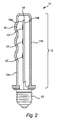
次に、照明デバイス11の側断面図を示す図2を参照する。この照明デバイス11は、図1で説明されたのと同様であるが、この場合には、ハウジング12の第2の部分12bから出る光からの角度発散を大きくするために第2の光学要素を有さず、基板14は、本発明の一実施形態による透過性材料14cを含む。第1の光学要素16を有するハウジング12の第1の部分12aは、図1で説明されたのと同様に構成されるが、光源13は、透光性PCB等の透光性基板14上に取り付けられている。
Reference is now made to FIG. 2 showing a side sectional view of the
基板14は、概して、可視光波長を透過するように構成される。従って、第1の光学要素16から反射された光は、ハウジング12の第2の部分12bに向けて透過性材料を透過され得る。第1の光学要素16を有するハウジング12の第1の部分12aの反対側に沿って配置されたハウジング12の第2の部分12bは、散乱粒子、例えば高散乱性の非吸収粒子、例えばTiO2、Al2O3、又はSiO2を含み得る。ハウジング12内の散乱粒子は、出射光を拡散して、より柔らかく、より一様に分散された光出力分布を提供し得る。散乱粒子は、シート内に組み込まれてよく、又は幾つかの層内に追加されて拡散性を実現してもよい。
The
更に、ハウジング12、特に、第1の光学要素16及びハウジング12の第1の部分12aは、散乱粒子、例えばTiO2、Al2O3、又はSiO2を含み得る。透過率は、入射光の量に対する、材料を透過される光の量によって決定される。散乱粒子の量は、透過される光の量、及び反射されて戻る光の量を決定し得る。散乱体の量の増加が、透過率を減少し得る。従って、幾つかの実施形態に関して、第1の光学要素16はハウジング12内に組み込まれ得る。散乱粒子の厚さは、反射率及び透過率を決定し得る。拡散部分は、シート内に組み込まれてよく、又は幾つかの層内に追加されて拡散性を実現してもよい。従って、散乱粒子の厚さ又は濃度の変化が、各第1の光学要素16にわたってされた反射率の大きさの変化を提供し得る。
Furthermore, the
図3を参照すると、本発明の一実施形態に従って、照明デバイス21の切欠側断面図が示されている。照明デバイス21の切欠側断面図は、電気コネクタ取付具25を有するコンパクトな照明デバイスの一部分を示す。照明デバイス21は、基板24を提供することによってコンパクトな照明デバイスを提供し、基板24は、第1の面24aに複数の光源23が取り付けられており、反対側、即ち基板の第2の面24bは、照明デバイスの基部25からハウジング22の周縁部へ、ハウジング22の第2の部分22bの内側に沿って取り付けられる。更に、ハウジング22の第1の部分22aの幾つかの部分が第1の基板の面24aに取り付けられてよく、更にコンパクトな照明デバイス21を提供する。
Referring to FIG. 3, a cutaway side cross-sectional view of
基板24は、貫通孔24cを有するように構成され、それにより、反射光は、第1の光学要素26から、ハウジング22の第2の部分22bに向けて、特に第2の光学要素27に向けて透過され得る。基板24に関連付けてハウジング22を配置することによって、コンパクトな照明デバイス21が提供され得る。第1の光学要素26は、図3に示される実施形態では、反射器とレンズの組合せである。
The
図3を参照すると、模式的な光線によって示されるように、第1の光学要素26の中央部は、光を反射するように構成され、第1の光学要素26の周縁部は、角度発散を大きくするために光を屈折するように構成されたレンズを備える。ハウジング22の第1の部分22aから出る光は、レンズによって屈折されて、出力光分布を広げる。屈折光路を表す模式的な光も図3に示されている。光源23から放出された光は、第1の光学要素26に達し、基板24の貫通孔24cに向けて反射される。反射光は、貫通孔24cを通って基板24を通過し、ハウジング22の第2の部分22bに向けて進み、第2の光学要素27を透過されて屈折され、それにより、ハウジング22の第2の部分22bから出る光に関する出力光分布が広げられる。
Referring to FIG. 3, the central portion of the first
幾つかの実施形態に関して、図3におけるように、第1の光学要素26及び第2の光学要素27は、それぞれハウジング22の第1の部分22a及びハウジング22の第2の部分22bに組み込まれ得る。
For some embodiments, as in FIG. 3, the first
ハウジング2、12、22、第1の光学要素6、16、26、及び/又は第2の光学要素7、27は、ポリマー材料、例えばポリメチルメタクリレート、PMMA、又はPC(ポリカーボネート)を含み得る。代替として、ハウジング2、12、22は、ガラスから形成されてもよい。光源3、13、23は、所定の方向に従って第1の光学要素6、16、26に向けて光を更に案内するために、一体化された光学要素、例えばレンズを含んでいてもよい。幾つかの実施形態では、第1の光学要素6、16、26はハウジング2、12、22の第1の部分2a、12a、22aに組み込まれてよく、従って、第1の光学要素6、16、26はレンズ形状及び反射部分を備えていてよく、この実施形態では、反射部分が第1の光学要素6、16、26の中央に配置され、一方、レンズは周縁部に提供されるが、逆も想定可能である。更に、第1の光学要素6、16、26は、幾つかの実施形態では、光の一部を反射するように構成された屈折コーティングを有する屈折レンズを備え得る。しかし、第1の光学要素6、16、26はまた、ハウジング2、12、22の第1の部分2a、12a、22aと光源3、13、23との間、即ちハウジング2、12、22の内部に配置されてもよい。
The
照明デバイス1、11、21は、レトロフィットの蛍光又は固体照明又は照明器具に関して特に有利であり得る。
The
用語「ハウジング2、12、22の第1の部分2a、12a、22a」は、一般に、取付具から突き出るハウジング2、12、22に沿って、突き出るハウジング2、12、22の端部に向かう側部として解釈されてよく、せいぜい、光源3、13、23の光出力方向で光源3、13、23の前に配置されたハウジングの一部分をカバーする。用語「ハウジング2、12、22の第2の部分2b、12b、22b」は、一般に、基部から突き出るハウジング2、12、22に沿って、突き出るハウジングの端部に向かう、ハウジングの第1の部分2a、12a、22aとは反対側の側部と解釈されてよい。ハウジングの第2の部分2b、12b、22bは、せいぜい、光源3、13、23の後ろ、従って光源3、13、23の光出力方向とは逆方向に配置されたハウジングの一部分をカバーする。
The term “
光源をドライブするためのドライバユニット又はドライバ回路(図示せず)が、基板4、14、24上に配置され得る。ドライバユニット及び/又はドライバ回路は、光の強度等、光源から放出される光の少なくとも1つのパラメータを修正するように適合され得る。ドライバ回路は、光源への電流及び電圧を制御する。ドライバ回路及び/又はドライバユニットは、更に、電気コネクタ取付具に電気的に接続される。ドライバ電子回路は、基板上に配置されてもよい。
A driver unit or driver circuit (not shown) for driving the light source may be disposed on the
本発明を、その特定の実施形態を参照して述べてきたが、多くの異なる変形や修正等が当業者には明らかになろう。例えば、幾つかの実施形態では、第1の光学要素6、16、26の反射部分が要素6、16、26の周縁部に配置され得て、一方、透過部分が第1の光学要素6、16、26の中央に配置される。システムの一部が省かれてよく、交換されてよく、又は様々な形で構成されてよく、それでもシステムが本発明の方法を実施することが可能であり得る。照明デバイスは、図1〜図3に示されるようなレトロフィット取付具を有する必要はなく、照明デバイスは、任意のタイプの照明器具に組み込まれてもよく、そのような照明器具は、例えば、シャンデリア照明器具、屋外都市景観照明器具、廊下の照明、及び全方位性の光分布から利益を得る他の平型の照明器具である。
Although the present invention has been described with reference to specific embodiments thereof, many different variations and modifications will become apparent to those skilled in the art. For example, in some embodiments, the reflective portion of the first
更に、図面、本開示、及び添付の特許請求の範囲を検討すれば、開示される実施形態に対する変形形態が、当業者には理解され得、本願で特許請求される発明を実践する際に実施され得る。特許請求の範囲において、用語「備える」は、他の要素又はステップを除外せず、「1つの」は、複数を除外しない。単一のプロセッサ又は他のユニットが、特許請求の範囲に記載される幾つかの要素の機能を実現することができる。特定の手段が相互に異なる従属請求項に記載されていることだけでは、これらの手段の組合せが有利に使用され得ないことを示さない。 Further, upon review of the drawings, the present disclosure, and the appended claims, variations to the disclosed embodiments can be understood by those skilled in the art and practiced in practicing the invention claimed herein. Can be done. In the claims, the term “comprising” does not exclude other elements or steps, and “a” does not exclude a plurality. A single processor or other unit may fulfill the functions of several elements recited in the claims. The mere fact that certain measures are recited in mutually different dependent claims does not indicate that a combination of these measured cannot be used to advantage.
Claims (15)
前記基板の前記第1の面に配置された複数の光源であって、共通の総合的出力方向を有する複数の光源と、
前記基板を取り囲む透光性材料から形成されたハウジングであって、前記ハウジングが光を透過し、前記ハウジングの第1の部分と、前記基板を挟んで前記第1の部分と実質的に反対側に配置された前記ハウジングの第2の部分とを有する、ハウジングと
を備える照明デバイスにおいて、
前記基板の前記第1の面に面する前記ハウジングの前記第1の部分に沿って、前記複数の光源の前記出力方向と実質的に向かい合うように配置された複数の第1の光学要素により特徴づけられ、
前記基板が、光の透過を可能にし、
前記複数の第1の光学要素が、前記光源によって放出された前記光の一部を透過し、且つ前記光源によって放出された前記光の一部を、前記基板を通して前記ハウジングの前記第2の部分に向けて反射し、
前記複数の第1の光学要素がそれぞれ、前記光源からの前記光を屈折及び反射する
ことを特徴とする、照明デバイス。 A substrate having a first surface and a second surface;
A plurality of light sources disposed on the first surface of the substrate, the light sources having a common overall output direction;
A housing formed of a light-transmitting material surrounding the substrate, wherein the housing transmits light, and is substantially opposite to the first portion of the housing and the first portion across the substrate; A lighting device comprising: a housing having a second portion of the housing disposed on the housing;
Characterized by a plurality of first optical elements disposed along the first portion of the housing facing the first surface of the substrate substantially opposite the output direction of the plurality of light sources. Attached,
The substrate allows light transmission;
The plurality of first optical elements transmit a portion of the light emitted by the light source and pass a portion of the light emitted by the light source through the substrate to the second portion of the housing. Reflected towards
The lighting device, wherein each of the plurality of first optical elements refracts and reflects the light from the light source.
Applications Claiming Priority (3)
| Application Number | Priority Date | Filing Date | Title |
|---|---|---|---|
| EP14153167.3 | 2014-01-30 | ||
| EP14153167 | 2014-01-30 | ||
| PCT/EP2015/050914 WO2015113852A1 (en) | 2014-01-30 | 2015-01-20 | Lighting device |
Publications (3)
| Publication Number | Publication Date |
|---|---|
| JP2017504944A true JP2017504944A (en) | 2017-02-09 |
| JP2017504944A5 JP2017504944A5 (en) | 2018-03-01 |
| JP6549595B2 JP6549595B2 (en) | 2019-07-24 |
Family
ID=50028856
Family Applications (1)
| Application Number | Title | Priority Date | Filing Date |
|---|---|---|---|
| JP2016549089A Active JP6549595B2 (en) | 2014-01-30 | 2015-01-20 | Lighting device |
Country Status (7)
| Country | Link |
|---|---|
| US (1) | US10655790B2 (en) |
| EP (1) | EP3105495B1 (en) |
| JP (1) | JP6549595B2 (en) |
| CN (1) | CN105960560B (en) |
| PL (1) | PL3105495T3 (en) |
| RU (1) | RU2707185C2 (en) |
| WO (1) | WO2015113852A1 (en) |
Families Citing this family (7)
| Publication number | Priority date | Publication date | Assignee | Title |
|---|---|---|---|---|
| US10845025B2 (en) * | 2016-09-29 | 2020-11-24 | Lumileds Llc | Lighting assembly with diffusor |
| DE102017110378B4 (en) * | 2017-05-12 | 2023-03-02 | Ledvance Gmbh | LED lamp with LED bulbs |
| DE102017115885A1 (en) | 2017-07-14 | 2019-01-17 | Ledvance Gmbh | LED bulb and LED bulb |
| JP2019161062A (en) * | 2018-03-14 | 2019-09-19 | 豊田合成株式会社 | Light-emitting device |
| IT201900005434A1 (en) * | 2019-04-09 | 2020-10-09 | Artemide Spa | LIGHTING DEVICE |
| WO2020227497A1 (en) * | 2019-05-09 | 2020-11-12 | Jeffway Jr Robert W | Two-sided illuminating printed circuit board assembly and illuminating device using the same |
| DE202022102261U1 (en) * | 2022-04-27 | 2023-08-07 | Thorn Lighting Limited | Panel light with rear (secondary) lighting |
Citations (2)
| Publication number | Priority date | Publication date | Assignee | Title |
|---|---|---|---|---|
| US20110235318A1 (en) * | 2010-03-26 | 2011-09-29 | Altair Engineering, Inc. | Led light tube with dual sided light distribution |
| JP2012238602A (en) * | 2010-11-04 | 2012-12-06 | Panasonic Corp | Bulb-shaped lamp and lighting system |
Family Cites Families (27)
| Publication number | Priority date | Publication date | Assignee | Title |
|---|---|---|---|---|
| US3610912A (en) * | 1968-08-14 | 1971-10-05 | Varian Associates | Low profile optical system |
| US3586851A (en) * | 1969-02-24 | 1971-06-22 | Robert R Rudolph | Cool light |
| US5947588A (en) * | 1997-10-06 | 1999-09-07 | Grand General Accessories Manufacturing Inc. | Light fixture with an LED light bulb having a conventional connection post |
| DE20018435U1 (en) | 2000-10-27 | 2001-02-22 | Shining Blick Entpr Co | Light bulb with bendable lamp bulbs contained therein |
| JP4076329B2 (en) * | 2001-08-13 | 2008-04-16 | エイテックス株式会社 | LED bulb |
| JP2005038822A (en) * | 2003-06-26 | 2005-02-10 | Sharp Corp | Lighting device for flat panel display and light-emitting lamp |
| JP4042687B2 (en) * | 2003-12-15 | 2008-02-06 | ソニー株式会社 | Lighting device and backlight device |
| US6948829B2 (en) * | 2004-01-28 | 2005-09-27 | Dialight Corporation | Light emitting diode (LED) light bulbs |
| JP2007165811A (en) * | 2005-12-16 | 2007-06-28 | Nichia Chem Ind Ltd | Light emitting device |
| KR20100093570A (en) * | 2007-11-20 | 2010-08-25 | 코닌클리즈케 필립스 일렉트로닉스 엔.브이. | Side emitting device with wavelength conversion |
| US8360599B2 (en) * | 2008-05-23 | 2013-01-29 | Ilumisys, Inc. | Electric shock resistant L.E.D. based light |
| CN101614329A (en) * | 2008-06-27 | 2009-12-30 | 富准精密工业(深圳)有限公司 | Led lamp and photo engine thereof |
| KR101155690B1 (en) | 2009-12-18 | 2012-06-12 | (주)아이디시스테크 | Small led lamp |
| US8833981B2 (en) * | 2010-04-23 | 2014-09-16 | Illumination Machines, Llc | Multiple-tier omnidirectional solid-state emission source |
| JP5545547B2 (en) * | 2010-10-07 | 2014-07-09 | 東芝ライテック株式会社 | Light source body and lighting apparatus |
| JP5276226B2 (en) * | 2010-10-22 | 2013-08-28 | パナソニック株式会社 | Mounting board, light emitting device and lamp |
| JP2012104295A (en) | 2010-11-08 | 2012-05-31 | Stanley Electric Co Ltd | Led lighting system |
| WO2012095758A2 (en) | 2011-01-11 | 2012-07-19 | Koninklijke Philips Electronics N.V. | Lighting device |
| US8714762B2 (en) * | 2011-05-03 | 2014-05-06 | Zhou Cai | LED light source and manufacturing method thereof |
| JP2012248687A (en) * | 2011-05-27 | 2012-12-13 | Toshiba Lighting & Technology Corp | Light-emitting module and illumination apparatus |
| US8324790B1 (en) * | 2011-06-07 | 2012-12-04 | Wen-Sung Hu | High illumination LED bulb with full emission angle |
| WO2013043743A1 (en) | 2011-09-19 | 2013-03-28 | Ruud Lighting, Inc. | Led retrofit lighting fixture |
| KR101344513B1 (en) * | 2012-02-07 | 2013-12-23 | 엘이디라이텍(주) | LED lamp assembly |
| US9395051B2 (en) * | 2012-04-13 | 2016-07-19 | Cree, Inc. | Gas cooled LED lamp |
| US8757839B2 (en) | 2012-04-13 | 2014-06-24 | Cree, Inc. | Gas cooled LED lamp |
| US20140168978A1 (en) * | 2012-12-17 | 2014-06-19 | Wen-Sung Hu | Full-Beam-Angle LED Bulb Structure |
| CN203348993U (en) * | 2013-06-26 | 2013-12-18 | 广东恒润光电有限公司 | Candle lamp |
-
2015
- 2015-01-20 US US15/115,060 patent/US10655790B2/en active Active
- 2015-01-20 CN CN201580006528.2A patent/CN105960560B/en active Active
- 2015-01-20 WO PCT/EP2015/050914 patent/WO2015113852A1/en active Application Filing
- 2015-01-20 JP JP2016549089A patent/JP6549595B2/en active Active
- 2015-01-20 PL PL15701156T patent/PL3105495T3/en unknown
- 2015-01-20 RU RU2016135041A patent/RU2707185C2/en active
- 2015-01-20 EP EP15701156.0A patent/EP3105495B1/en active Active
Patent Citations (2)
| Publication number | Priority date | Publication date | Assignee | Title |
|---|---|---|---|---|
| US20110235318A1 (en) * | 2010-03-26 | 2011-09-29 | Altair Engineering, Inc. | Led light tube with dual sided light distribution |
| JP2012238602A (en) * | 2010-11-04 | 2012-12-06 | Panasonic Corp | Bulb-shaped lamp and lighting system |
Also Published As
| Publication number | Publication date |
|---|---|
| CN105960560A (en) | 2016-09-21 |
| US10655790B2 (en) | 2020-05-19 |
| RU2016135041A3 (en) | 2018-09-13 |
| CN105960560B (en) | 2020-01-07 |
| EP3105495B1 (en) | 2017-11-01 |
| RU2016135041A (en) | 2018-03-05 |
| WO2015113852A1 (en) | 2015-08-06 |
| JP6549595B2 (en) | 2019-07-24 |
| EP3105495A1 (en) | 2016-12-21 |
| RU2707185C2 (en) | 2019-11-25 |
| US20160348852A1 (en) | 2016-12-01 |
| PL3105495T3 (en) | 2018-04-30 |
Similar Documents
| Publication | Publication Date | Title |
|---|---|---|
| JP6549595B2 (en) | Lighting device | |
| RU2519278C2 (en) | Light source with light-emitting diodes, beamguide and reflector | |
| JP5711147B2 (en) | Light source with LED, light guide and reflector | |
| US8602621B2 (en) | Optical element and light source comprising the same | |
| EP3063466B1 (en) | Illumination device for direct-indirect illumination | |
| JP5647274B2 (en) | Light mixing module and luminaire having such a light mixing module | |
| US20110249467A1 (en) | Light emitting device creating decorative light effects in a luminaire | |
| US10480721B2 (en) | Light flux controlling member, light emitting device and illuminating device | |
| JP2012160666A (en) | Light source module and lighting device | |
| JP2014103062A (en) | Lighting fixture | |
| JP6072785B2 (en) | Optical waveguide | |
| JP2017050187A (en) | Lighting fixture | |
| US10190730B2 (en) | Light flux controlling member, light emitting device and illuminating device | |
| WO2015129671A1 (en) | Lighting apparatus, light source cover, light control member, and light source unit | |
| JP2015162447A (en) | Lighting device and light source cover | |
| US10066793B2 (en) | LED luminaire | |
| JP7300879B2 (en) | Optical lens, light source device and illumination device | |
| WO2016181789A1 (en) | Light beam control member, light-emitting device, and illumination device | |
| JP6386808B2 (en) | Lighting device | |
| TWM481334U (en) | A light Engine device | |
| JP2015170604A (en) | Light source device and lighting device |
Legal Events
| Date | Code | Title | Description |
|---|---|---|---|
| A521 | Request for written amendment filed |
Free format text: JAPANESE INTERMEDIATE CODE: A523 Effective date: 20180118 |
|
| A621 | Written request for application examination |
Free format text: JAPANESE INTERMEDIATE CODE: A621 Effective date: 20180118 |
|
| A977 | Report on retrieval |
Free format text: JAPANESE INTERMEDIATE CODE: A971007 Effective date: 20180910 |
|
| A131 | Notification of reasons for refusal |
Free format text: JAPANESE INTERMEDIATE CODE: A131 Effective date: 20180918 |
|
| RD02 | Notification of acceptance of power of attorney |
Free format text: JAPANESE INTERMEDIATE CODE: A7422 Effective date: 20180921 |
|
| RD04 | Notification of resignation of power of attorney |
Free format text: JAPANESE INTERMEDIATE CODE: A7424 Effective date: 20181009 |
|
| A601 | Written request for extension of time |
Free format text: JAPANESE INTERMEDIATE CODE: A601 Effective date: 20181218 |
|
| TRDD | Decision of grant or rejection written | ||
| A01 | Written decision to grant a patent or to grant a registration (utility model) |
Free format text: JAPANESE INTERMEDIATE CODE: A01 Effective date: 20190531 |
|
| A61 | First payment of annual fees (during grant procedure) |
Free format text: JAPANESE INTERMEDIATE CODE: A61 Effective date: 20190627 |
|
| R150 | Certificate of patent or registration of utility model |
Ref document number: 6549595 Country of ref document: JP Free format text: JAPANESE INTERMEDIATE CODE: R150 |
|
| R250 | Receipt of annual fees |
Free format text: JAPANESE INTERMEDIATE CODE: R250 |