JP2017120364A - Projector, electronic apparatus having the projector, and manufacturing method related thereto - Google Patents
Projector, electronic apparatus having the projector, and manufacturing method related thereto Download PDFInfo
- Publication number
- JP2017120364A JP2017120364A JP2016110556A JP2016110556A JP2017120364A JP 2017120364 A JP2017120364 A JP 2017120364A JP 2016110556 A JP2016110556 A JP 2016110556A JP 2016110556 A JP2016110556 A JP 2016110556A JP 2017120364 A JP2017120364 A JP 2017120364A
- Authority
- JP
- Japan
- Prior art keywords
- substrate
- laser beam
- projector
- collimator lens
- optical element
- Prior art date
- Legal status (The legal status is an assumption and is not a legal conclusion. Google has not performed a legal analysis and makes no representation as to the accuracy of the status listed.)
- Pending
Links
Images


Classifications
-
- H—ELECTRICITY
- H04—ELECTRIC COMMUNICATION TECHNIQUE
- H04N—PICTORIAL COMMUNICATION, e.g. TELEVISION
- H04N9/00—Details of colour television systems
- H04N9/12—Picture reproducers
- H04N9/31—Projection devices for colour picture display, e.g. using electronic spatial light modulators [ESLM]
- H04N9/3141—Constructional details thereof
- H04N9/315—Modulator illumination systems
- H04N9/3161—Modulator illumination systems using laser light sources
-
- G—PHYSICS
- G01—MEASURING; TESTING
- G01B—MEASURING LENGTH, THICKNESS OR SIMILAR LINEAR DIMENSIONS; MEASURING ANGLES; MEASURING AREAS; MEASURING IRREGULARITIES OF SURFACES OR CONTOURS
- G01B11/00—Measuring arrangements characterised by the use of optical techniques
- G01B11/22—Measuring arrangements characterised by the use of optical techniques for measuring depth
-
- G—PHYSICS
- G01—MEASURING; TESTING
- G01B—MEASURING LENGTH, THICKNESS OR SIMILAR LINEAR DIMENSIONS; MEASURING ANGLES; MEASURING AREAS; MEASURING IRREGULARITIES OF SURFACES OR CONTOURS
- G01B11/00—Measuring arrangements characterised by the use of optical techniques
- G01B11/24—Measuring arrangements characterised by the use of optical techniques for measuring contours or curvatures
- G01B11/25—Measuring arrangements characterised by the use of optical techniques for measuring contours or curvatures by projecting a pattern, e.g. one or more lines, moiré fringes on the object
-
- G—PHYSICS
- G02—OPTICS
- G02B—OPTICAL ELEMENTS, SYSTEMS OR APPARATUS
- G02B13/00—Optical objectives specially designed for the purposes specified below
- G02B13/001—Miniaturised objectives for electronic devices, e.g. portable telephones, webcams, PDAs, small digital cameras
- G02B13/0055—Miniaturised objectives for electronic devices, e.g. portable telephones, webcams, PDAs, small digital cameras employing a special optical element
-
- G—PHYSICS
- G02—OPTICS
- G02B—OPTICAL ELEMENTS, SYSTEMS OR APPARATUS
- G02B13/00—Optical objectives specially designed for the purposes specified below
- G02B13/001—Miniaturised objectives for electronic devices, e.g. portable telephones, webcams, PDAs, small digital cameras
- G02B13/0085—Miniaturised objectives for electronic devices, e.g. portable telephones, webcams, PDAs, small digital cameras employing wafer level optics
-
- G—PHYSICS
- G02—OPTICS
- G02B—OPTICAL ELEMENTS, SYSTEMS OR APPARATUS
- G02B27/00—Optical systems or apparatus not provided for by any of the groups G02B1/00 - G02B26/00, G02B30/00
- G02B27/30—Collimators
-
- G—PHYSICS
- G02—OPTICS
- G02B—OPTICAL ELEMENTS, SYSTEMS OR APPARATUS
- G02B5/00—Optical elements other than lenses
- G02B5/18—Diffraction gratings
- G02B5/1842—Gratings for image generation
-
- G—PHYSICS
- G02—OPTICS
- G02B—OPTICAL ELEMENTS, SYSTEMS OR APPARATUS
- G02B5/00—Optical elements other than lenses
- G02B5/18—Diffraction gratings
- G02B5/1847—Manufacturing methods
- G02B5/1852—Manufacturing methods using mechanical means, e.g. ruling with diamond tool, moulding
-
- G—PHYSICS
- G03—PHOTOGRAPHY; CINEMATOGRAPHY; ANALOGOUS TECHNIQUES USING WAVES OTHER THAN OPTICAL WAVES; ELECTROGRAPHY; HOLOGRAPHY
- G03B—APPARATUS OR ARRANGEMENTS FOR TAKING PHOTOGRAPHS OR FOR PROJECTING OR VIEWING THEM; APPARATUS OR ARRANGEMENTS EMPLOYING ANALOGOUS TECHNIQUES USING WAVES OTHER THAN OPTICAL WAVES; ACCESSORIES THEREFOR
- G03B21/00—Projectors or projection-type viewers; Accessories therefor
- G03B21/14—Details
- G03B21/20—Lamp housings
- G03B21/2006—Lamp housings characterised by the light source
- G03B21/2033—LED or laser light sources
-
- G—PHYSICS
- G03—PHOTOGRAPHY; CINEMATOGRAPHY; ANALOGOUS TECHNIQUES USING WAVES OTHER THAN OPTICAL WAVES; ELECTROGRAPHY; HOLOGRAPHY
- G03B—APPARATUS OR ARRANGEMENTS FOR TAKING PHOTOGRAPHS OR FOR PROJECTING OR VIEWING THEM; APPARATUS OR ARRANGEMENTS EMPLOYING ANALOGOUS TECHNIQUES USING WAVES OTHER THAN OPTICAL WAVES; ACCESSORIES THEREFOR
- G03B21/00—Projectors or projection-type viewers; Accessories therefor
- G03B21/14—Details
- G03B21/20—Lamp housings
- G03B21/206—Control of light source other than position or intensity
-
- H—ELECTRICITY
- H04—ELECTRIC COMMUNICATION TECHNIQUE
- H04N—PICTORIAL COMMUNICATION, e.g. TELEVISION
- H04N5/00—Details of television systems
- H04N5/30—Transforming light or analogous information into electric information
- H04N5/33—Transforming infrared radiation
-
- H—ELECTRICITY
- H04—ELECTRIC COMMUNICATION TECHNIQUE
- H04N—PICTORIAL COMMUNICATION, e.g. TELEVISION
- H04N9/00—Details of colour television systems
- H04N9/12—Picture reproducers
- H04N9/31—Projection devices for colour picture display, e.g. using electronic spatial light modulators [ESLM]
- H04N9/3179—Video signal processing therefor
Abstract
Description
本発明はプロジェクタに関し、より具体的には回折光学素子を有するプロジェクタに関する。 The present invention relates to a projector, and more specifically to a projector having a diffractive optical element.
従来のプロジェクタは概して、投影画像を生成するためにレーザー光源、コリメーター、回折光学素子及び反射器/プリズムを有することが必要であり、これらの4つの素子はプロジェクタ内の独立した部品である。しかしながら、スマートフォン又はパッドのような電子機器が更に薄くなるため、これらの素子を有するプロジェクタの寸法は、その電子機器の中に配置されるためには大き過ぎ、プロジェクタ設計に困難性を生じさせる。 Conventional projectors generally require a laser light source, a collimator, a diffractive optical element, and a reflector / prism to generate a projected image, and these four elements are independent components within the projector. However, as electronic devices such as smartphones or pads become thinner, the size of a projector having these elements is too large to be placed in the electronic device, creating difficulties in projector design.
加えて、電子器機が3D画像を記録(capture)しようとする場合は、立体情報を計算するために、異なる角度をもつ二つの画像を記録するために二つのカメラモジュールが要求される。しかしながら、二つのカメラモジュールは製造コストを増大させるかも知れず、立体情報の計算は電子機器内のプロセッサの負荷を著しく増大させるかも知れない。 In addition, if the electronic device is to capture a 3D image, two camera modules are required to record two images with different angles in order to calculate stereoscopic information. However, the two camera modules may increase the manufacturing cost, and the calculation of stereoscopic information may significantly increase the processor load in the electronic device.
したがって、本発明の一つの目的は、上述の課題を解決するために、プリズム又は反射素子を持たず厚さが小さい、内部の基板上にインプリントされた(imprinted)回折光学素子を有するプロジェクタを提供することである。 Accordingly, one object of the present invention is to provide a projector having a diffractive optical element imprinted on an internal substrate having a small thickness without a prism or a reflective element, in order to solve the above-described problems. Is to provide.
本発明の一つの実施形態によれば、プロジェクタは、レーザービームを生成するためのレーザーモジュール及びウエハレベル光学系(wafer-level optics)を有する。ウエハレベル光学系は、第一基板、第一コリメータレンズ及び回折光学素子を有する。第一コリメータレンズは、前記第一基板の第一表面上に製造されており、レーザーモジュールからレーザービームを受けて平行化レーザービーム(collimated laser beam)を生成するように構成されている。平行化レーザービームは、回折光学素子を直接的に通過してプロジェクタの投影画像を生成する。 According to one embodiment of the present invention, the projector has a laser module and wafer-level optics for generating a laser beam. The wafer level optical system has a first substrate, a first collimator lens, and a diffractive optical element. The first collimator lens is manufactured on the first surface of the first substrate, and is configured to receive a laser beam from the laser module and generate a collimated laser beam. The collimated laser beam passes directly through the diffractive optical element and generates a projection image of the projector.
本発明の他の実施形態によれば、電子器機は、プロジェクタ、カメラモジュール及びプロセッサを有する。プロジェクタは、レーザービームを生成するためのレーザーモジュール及びウエハレベル光学系を有する。ウエハレベル光学系は、第一基板、第一コリメータレンズ及び回折光学素子を有する。レーザービームは、第一コリメータレンズ及び回折光学素子を直接的に通過して、周囲環境の領域にプロジェクタの投影画像を生成する。カメラモジュールは、周囲環境の領域を記録して画像データを生成するように構成されている。プロセッサは、画像データを分析して画像データの立体情報(depth information)を取得するように構成されている。 According to another embodiment of the present invention, an electronic device includes a projector, a camera module, and a processor. The projector has a laser module and a wafer level optical system for generating a laser beam. The wafer level optical system has a first substrate, a first collimator lens, and a diffractive optical element. The laser beam directly passes through the first collimator lens and the diffractive optical element, and generates a projection image of the projector in the area of the surrounding environment. The camera module is configured to record the area of the surrounding environment and generate image data. The processor is configured to analyze the image data and obtain stereoscopic information (depth information) of the image data.
本発明の他の実施形態によれば、プロジェクタを製造する方法は:第一基板を提供するステップ;第一基板上に第一コリメータレンズを製造するステップ;第二基板を提供するステップ;第二基板上に回折光学素子をインプリントするステップ;及びレーザーモジュールによって生成されたレーザービームに第一コリメータレンズ及び回折光学素子を直接的に通過させてプロジェクタの投影画像を生成するように、第一基板、第二基板及びレーザーモジュールを組み立てるステップ、を含む。 According to another embodiment of the present invention, a method of manufacturing a projector includes: providing a first substrate; manufacturing a first collimator lens on the first substrate; providing a second substrate; Imprinting a diffractive optical element on the substrate; and passing the first collimator lens and the diffractive optical element directly through the laser beam generated by the laser module to generate a projection image of the projector. Assembling the second substrate and the laser module.
本発明のこれらの目的及び他の目的は、様々な図表及び図面に示される好ましい実施形態の以下の詳細な説明を読んだ後に、疑いなく、当業者にとって明らかになるであろう。 These and other objects of the present invention will no doubt become apparent to those skilled in the art after reading the following detailed description of the preferred embodiments shown in the various diagrams and drawings.
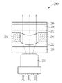
図1を参照されたい。図1は、本発明の第一の実施形態によるプロジェクタ100を示す図である。図1に示されるように、プロジェクタ100は、レーザーモジュール110及びウエハレベル光学系(又はウエハレベルオプティクス)を有する。ここで、ウエハレベル光学系は、基板120、基板120の表面上にインプリントされたコリメータレンズ122、基板130、基板130の表面上にインプリントされたコリメータレンズ132、基板130の他の表面上にインプリントされた回折光学素子(diffractive optical element)(DOE)140、及びスペーサ150を有する。本実施形態において、プロジェクタ100は特有のパターンの画像を投影する(project)するように構成されており、プロジェクタ100はスマートフォン又はパッドのような電子機器内に配置されている。
Please refer to FIG. FIG. 1 is a diagram showing a
図1に示されるプロジェクタ100において、レーザーモジュール110はレーザービームを生成するように構成されており、具体的には、レーザービームは赤外光である。コリメータレンズ122及び132は、凸レンズであり、レーザーモジュール110からレーザービームを受けて平行化レーザービーム(平行光線(parallel rays))を生成するように構成されている。ここで、平行化レーザービームは、基板130及びDOE140の表面に対して実質的に垂直である。DOE140はパターン生成装置として機能することができ、平行化レーザービームは、DOE140を直接的に通過して投影画像(projected image)を生成する。ここで、投影画像は、DOE140によって設定された特有のパターンを有し得る。
In the
図1に示される実施形態において、レーザービームはコリメータレンズ122及び132並びにDOE140を直接的に通過して特有のパターンを有する投影画像になり、レーザービームは、如何なるプリズム又は反射/屈折素子によっても方向付けられない(not directed)。この構造を使用することによって、プロジェクタ100は、厚さが小さく、より薄い電子機器の中に配置されることができる。
In the embodiment shown in FIG. 1, the laser beam passes directly through the
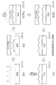
図2を参照されたい。図2は、本発明の第二の実施形態によるプロジェクタ200を示す図である。図2に示されるように、プロジェクタ200は、レーザーモジュール210及びウエハレベル光学系を有する。ここで、ウエハレベル光学系は、基板220、基板220の表面上にインプリントされた凹面コリメータレンズ222、基板230、基板230の表面上にインプリントされた凸面コリメータレンズ232、基板230の他の表面上にインプリントされたDOE240、及びスペーサ250を有する。プロジェクタ200は、コリメータレンズ222が凹レンズであることを除いて、図1に示されるプロジェクタ100と同様である。
Please refer to FIG. FIG. 2 is a diagram showing a
一つの代替的な実施形態において、コリメータレンズ222が凸レンズであって、一方でコリメータレンズ232が凹レンズであってもよい。
In one alternative embodiment, the
図3を参照されたい。図3は、本発明の第三の実施形態によるプロジェクタ300を示す図である。図3に示されるように、プロジェクタ300は、レーザーモジュール310及びウエハレベル光学系を有する。ここで、ウエハレベル光学系は、基板320、基板320の表面上にインプリントされた凸面コリメータレンズ322、基板330、基板330の表面上にインプリントされたDOE340、及びスペーサ350を有する。プロジェクタ300は、基板330の表面上にコリメータレンズが製造されていないことを除いて、図1に示されるプロジェクタ100と同様である。
Please refer to FIG. FIG. 3 is a diagram showing a
図4を参照されたい。図4は、本発明の第四の実施形態によるプロジェクタ400を示す図である。図4に示されるように、プロジェクタ400は、レーザーモジュール410及びウエハレベル光学系を有する。ここで、ウエハレベル光学系は、基板420、基板420の表面上にインプリントされた凸面コリメータレンズ422、基板420の他の表面上にインプリントされた他の凸面コリメータレンズ424、基板430、基板430の表面上にインプリントされたDOE440、及びスペーサ450を有する。プロジェクタ400は、基板430の二つの反対側の表面上に二つのコリメータレンズ422及び424が製造されていることを除いて、図3に示されるプロジェクタ300と同様である。
Please refer to FIG. FIG. 4 is a diagram showing a
一つの代替的な実施形態において、コリメータレンズ422及び424のうちの一方が凸レンズであって、一方でコリメータレンズ422及び424のうちの他方が凹レンズであってもよい。
In one alternative embodiment, one of the
上記の複数の実施形態において、DOE140/240/340/440は、ナノインプリント半導体リソグラフィーによって製造される。図5は、本発明の一つの実施形態によるDOE140/240/340/440の部分の側面図及び上面図を示す。 In the above embodiments, the DOE 140/240/340/440 is manufactured by nanoimprint semiconductor lithography. FIG. 5 shows side and top views of portions of DOE 140/240/340/440 according to one embodiment of the present invention.
図6乃至図8は、本発明の一つの実施形態による、図1に示されるウエハレベル光学系の製造方法を示す。図6は、それぞれ基板120及び130へのコリメータレンズ122及び132のインプリンティングの詳細を示す。図6に示されるように、洗浄(cleaning)ステップにおいて、基板120/130は、更なる工程(process)のために洗浄される。成形(molding)ステップにおいて、紫外線(UV)硬化性ポリマーが基板120/130の表面上に注入又は分配され、UV硬化性ポリマーを形作るために加工用型(working stamp)が使用される。UV硬化(curing)ステップにおいて、UV硬化性ポリマーを硬化させるために紫外線が使用される。ここで、硬化した層は、コリメータレンズ122/132として機能する。脱成形(de-molding)ステップにおいて、加工用型が取り外される。続くステップにおいて、端部残留物除去及び洗浄ステップが実行される。検査ステップにおいて、突発故障(catastrophic failure)及び品質欠陥の両方に関して試験下の基板120/130をスキャンするために自動光学検査(automated optical inspection)(AOI)が使用される。図6に示されるステップを使用することにより、図1に示されるコリメータレンズ122を備えた基板120及びコリメータレンズ132を備えた基板130が、作られる。
6 to 8 illustrate a method for manufacturing the wafer level optical system shown in FIG. 1 according to one embodiment of the present invention. FIG. 6 shows details of the imprinting of the
図7は、基板120及び130の組立ての詳細を示す。第一のステップにおいて、基板130は、スペーサ150と接合される(bonded)。続く積み重ね(stacking)ステップにおいて、電荷結合素子(charge-coupled device)(CCD)整列システムを使用することによって、基板120は、スペーサ150を介して基板130と組み立てられる。続くステップにおいて、レンズの映写性能(image performance)を検査するために、変調伝達関数(modulation transfer function)(MTF)試験が実行される。
FIG. 7 shows details of the assembly of the
図8は、DOE140のインプリンティング及び続く組み立てステップの詳細を示す。図8に示されるように、第一のステップにおいて、UV硬化性ポリマーが基板130の表面上に注入又は分配され、CCD整列システムを使用することによってUV硬化性ポリマーを形作るためにDOE加工用型が使用される。第二のステップにおいて、UV硬化性ポリマーを硬化させるために紫外線が使用される。ここで、硬化した層は、DOE140として機能する。第三のステップにおいて、DOE加工用型が取り外される。第四のステップにおいて、組み立てられたデバイスは複数の四角形の片にさいの目に切られる(diced)。ここで、各四角形は、図1に示されるウエハレベル光学系として機能する。第五のステップにおいて、突発故障及び品質欠陥の両方に関して試験下の基板120/130をスキャンするためにAOIが使用される。最後に、四角形の片(すなわち、複数のウエハレベル光学系)は、更なる工程のために仕分けられる(sorted)。
FIG. 8 shows details of the
図2乃至図4に示される実施形態は、図6乃至図8に示されるステップと同様のステップによって製造され得る。当業者は、上述の開示を読んだ後に図2乃至図4に示される実施形態の製造ステップを理解するであろうから、更なる説明はここでは省略する。 The embodiment shown in FIGS. 2-4 can be manufactured by steps similar to those shown in FIGS. 6-8. Since those skilled in the art will understand the manufacturing steps of the embodiment shown in FIGS. 2-4 after reading the above disclosure, further description is omitted here.
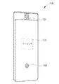
図9は、本発明の一つの実施形態による電子機器900を示す図である。図9に示されるように、電子機器900はスマートフォンであり、電子機器900はプロジェクタ910、カメラモジュール920及びプロセッサ930を有する。本実施形態において、プロジェクタ910は図1乃至図4に示されるプロジェクタのいずれかによって実施されてもよく、プロジェクタ910は、電子機器900の背面に埋め込まれており、周囲環境の領域に特有のパターンを持つ赤外画像を投影するために使用される。次いで、カメラモジュール920は、周囲環境の領域を記録して画像データを生成する。最後に、プロセッサ930は、画像データを分析して画像データの立体情報を取得する。図9に示される実施形態において、電子機器900は、プロジェクタ920及び一つのカメラモジュール930のみを使用することによって、3D画像を単純に生成してもよい。
FIG. 9 is a diagram illustrating an
簡単に要約すると、本発明のプロジェクタにおいて、プロジェクタの内部基板上へのDOEのインプリンティングによって、プロジェクタの厚さは、より薄い電子機器の中に埋め込められるために十分に小さい。加えて、本発明のプロジェクタを電子機器に使用することによって、電子機器は、一つのカメラモジュールによって記録された画像をただ単に分析することにより、3D画像を構築することができる。故に、製造コスト及びプロセッサの負荷が、改善されることができる。 Briefly summarized, in the projector of the present invention, the thickness of the projector is sufficiently small to be embedded in thinner electronic equipment by imprinting the DOE onto the internal substrate of the projector. In addition, by using the projector of the present invention for an electronic device, the electronic device can construct a 3D image by simply analyzing the image recorded by one camera module. Hence, manufacturing costs and processor load can be improved.
当業者は、本発明の教示を維持したまま、そのデバイス及び方法の多数の変更及び代替が成され得ることを容易に観察するであろう。したがって、上記の開示は、添付の特許請求の範囲の境界によってのみ限定されるものとして解釈されるべきである。
Those skilled in the art will readily observe that numerous modifications and substitutions of the device and method can be made while maintaining the teachings of the present invention. Accordingly, the above disclosure should be construed as limited only by the metes and bounds of the appended claims.
Claims (22)
レーザービームを生成するためのレーザーモジュール、並びに
ウエハレベル光学系であり、当該ウエハレベル光学系は、
第一基板、
前記レーザーモジュールから前記レーザービームを受けて平行化レーザービームを生成するための、前記第一基板の第一表面上に製造された第一コリメータレンズ、及び
回折光学素子であり、前記平行化レーザービームは前記回折光学素子を直接的に通過して当該プロジェクタの投影画像を生成する、回折光学素子、
を有する、ウエハレベル光学系、
を有する、プロジェクタ。 A projector,
A laser module for generating a laser beam, and a wafer level optical system, the wafer level optical system,
First substrate,
A first collimator lens manufactured on a first surface of the first substrate for receiving the laser beam from the laser module and generating a collimated laser beam; and a diffractive optical element; Is a diffractive optical element that directly passes through the diffractive optical element to generate a projection image of the projector,
A wafer level optical system,
Having a projector.
第二基板であり、前記回折光学素子は前記第二基板の表面にインプリントされており、前記第二基板の前記表面は、前記平行化レーザービームに対して実質的に垂直である、第二基板、
を更に有する、請求項1に記載のプロジェクタ。 The wafer level optical system includes:
A second substrate, wherein the diffractive optical element is imprinted on a surface of the second substrate, and the surface of the second substrate is substantially perpendicular to the collimated laser beam; substrate,
The projector according to claim 1, further comprising:
前記第一コリメータレンズ及び前記第二コリメータレンズは、前記レーザーモジュールから前記レーザービームを受けて前記平行化レーザービームを生成する、
請求項5に記載のプロジェクタ。 The wafer level optical system further includes a second collimator lens manufactured on the other surface of the second substrate,
The first collimator lens and the second collimator lens receive the laser beam from the laser module and generate the collimated laser beam.
The projector according to claim 5.
プロジェクタであり、当該プロジェクタは、
レーザービームを生成するためのレーザーモジュール、及び
第一コリメータレンズ及び回折光学素子を有するウエハレベル光学系であり、レーザービームは前記第一コリメータレンズ及び前記回折光学素子を直接的に通過して、周囲環境の領域に当該プロジェクタの投影画像を生成する、ウエハレベル光学系、
を有する、プロジェクタ、
前記周囲環境の前記領域を記録して画像データを生成するための、カメラモジュール、並びに
前記画像データを分析して前記画像データの立体情報を取得するための、プロセッサ、
を有する、電子機器。 Electronic equipment,
A projector, the projector
A laser module for generating a laser beam, and a wafer level optical system having a first collimator lens and a diffractive optical element, wherein the laser beam directly passes through the first collimator lens and the diffractive optical element A wafer level optical system for generating a projection image of the projector in the environment area,
Having a projector,
A camera module for recording the region of the surrounding environment and generating image data; and a processor for analyzing the image data and obtaining stereoscopic information of the image data;
Having an electronic device.
第一基板であり、前記第一コリメータレンズは前記第一基板の第一表面上に製造されており、前記第一コリメータレンズは前記レーザーモジュールから前記レーザービームを受けて平行化レーザービームを生成するように構成されており、前記平行化レーザービームは前記回折光学素子を直接的に通過して前記プロジェクタの投影画像を生成する、第一基板、を有する、
請求項9に記載の電子機器。 The wafer level optical system includes:
A first substrate, wherein the first collimator lens is fabricated on a first surface of the first substrate, and the first collimator lens receives the laser beam from the laser module and generates a collimated laser beam. The collimated laser beam directly passes through the diffractive optical element to generate a projection image of the projector, and has a first substrate.
The electronic device according to claim 9.
第二基板であり、前記回折光学素子は前記第二基板の表面にインプリントされており、前記第二基板の前記表面は、前記平行化レーザービームに対して実質的に垂直である、第二基板、
を更に有する、請求項10に記載の電子機器。 The wafer level optical system includes:
A second substrate, wherein the diffractive optical element is imprinted on a surface of the second substrate, and the surface of the second substrate is substantially perpendicular to the collimated laser beam; substrate,
The electronic device according to claim 10, further comprising:
前記第一コリメータレンズ及び前記第二コリメータレンズは、前記レーザーモジュールから前記レーザービームを受けて前記平行化レーザービームを生成する、
請求項14に記載の電子機器。 The wafer level optical system further includes a second collimator lens manufactured on the other surface of the second substrate,
The first collimator lens and the second collimator lens receive the laser beam from the laser module and generate the collimated laser beam.
The electronic device according to claim 14.
第一基板を提供するステップ、
前記第一基板上に第一コリメータレンズを製造するステップ、
第二基板を提供するステップ、
前記第二基板上に回折光学素子をインプリントするステップ、及び
レーザーモジュールによって生成されたレーザービームに前記第一コリメータレンズ及び前記回折光学素子を直接的に通過させて前記プロジェクタの投影画像を生成するように、前記第一基板、前記第二基板及び前記レーザーモジュールを組み立てるステップ、
を含む、方法。 A method of manufacturing a projector, comprising:
Providing a first substrate;
Producing a first collimator lens on the first substrate;
Providing a second substrate;
Imprinting a diffractive optical element on the second substrate; and passing the first collimator lens and the diffractive optical element directly through a laser beam generated by a laser module to generate a projection image of the projector Assembling the first substrate, the second substrate and the laser module,
Including the method.
前記第二基板の第二表面上に第二コリメータレンズを製造するステップであり、前記第二表面は前記第一表面の反対側である、ステップ、
を更に含む、請求項18に記載の方法。 The diffractive optical element is imprinted on the first surface of the second substrate, and the method includes:
Manufacturing a second collimator lens on a second surface of the second substrate, wherein the second surface is opposite the first surface;
The method of claim 18, further comprising:
The method of claim 18, wherein the laser beam is infrared light.
Applications Claiming Priority (2)
| Application Number | Priority Date | Filing Date | Title |
|---|---|---|---|
| US201562271354P | 2015-12-28 | 2015-12-28 | |
| US62/271,354 | 2015-12-28 |
Publications (1)
| Publication Number | Publication Date |
|---|---|
| JP2017120364A true JP2017120364A (en) | 2017-07-06 |
Family
ID=56296534
Family Applications (1)
| Application Number | Title | Priority Date | Filing Date |
|---|---|---|---|
| JP2016110556A Pending JP2017120364A (en) | 2015-12-28 | 2016-06-02 | Projector, electronic apparatus having the projector, and manufacturing method related thereto |
Country Status (6)
| Country | Link |
|---|---|
| US (2) | US20170187997A1 (en) |
| EP (1) | EP3200000A1 (en) |
| JP (1) | JP2017120364A (en) |
| KR (1) | KR20170077761A (en) |
| CN (1) | CN106918977A (en) |
| TW (1) | TWI621904B (en) |
Cited By (3)
| Publication number | Priority date | Publication date | Assignee | Title |
|---|---|---|---|---|
| JP2019079039A (en) * | 2017-10-20 | 2019-05-23 | 奇景光電股▲ふん▼有限公司 | Method for controlling projector and related electronic device |
| JP2020020861A (en) * | 2018-07-30 | 2020-02-06 | 奇景光電股▲ふん▼有限公司 | Projector, electronic device having the same, and associated manufacturing method |
| US10714891B2 (en) | 2018-07-06 | 2020-07-14 | Himax Technologies Limited | Projector, electronic device having projector and associated manufacturing method |
Families Citing this family (20)
| Publication number | Priority date | Publication date | Assignee | Title |
|---|---|---|---|---|
| US10241244B2 (en) | 2016-07-29 | 2019-03-26 | Lumentum Operations Llc | Thin film total internal reflection diffraction grating for single polarization or dual polarization |
| CN109839792A (en) * | 2017-11-25 | 2019-06-04 | 宁波舜宇光电信息有限公司 | The structured light projecting device, electronic equipment and its application for having encoded light |
| US10841547B2 (en) * | 2018-01-09 | 2020-11-17 | Himax Technologies Limited | Method for fabricating small right angle prism mirrors involving 3D shape on optical glue layer |
| CN110068983A (en) * | 2018-01-24 | 2019-07-30 | 宁波舜宇光电信息有限公司 | Structured light projecting device |
| CN108255000A (en) * | 2018-01-26 | 2018-07-06 | 深圳奥比中光科技有限公司 | Optical projection apparatus containing wafer lens |
| CN108181777A (en) * | 2018-02-27 | 2018-06-19 | 广东欧珀移动通信有限公司 | Laser projection module, depth camera and electronic device |
| CN108344377B (en) * | 2018-03-12 | 2020-05-15 | Oppo广东移动通信有限公司 | Laser projection module, depth camera and electronic device |
| EP3567426B1 (en) * | 2018-03-12 | 2021-07-07 | Guangdong Oppo Mobile Telecommunications Corp., Ltd. | Laser projection module, depth camera, and electronic device |
| CN108535828A (en) * | 2018-03-12 | 2018-09-14 | 广东欧珀移动通信有限公司 | Diffraction optical assembly, laser projection module, depth camera and electronic device |
| NL2020697B1 (en) * | 2018-03-30 | 2019-10-07 | Anteryon Wafer Optics B V | optical module |
| CN108594562A (en) * | 2018-04-02 | 2018-09-28 | 浙江舜宇光学有限公司 | Project module and projecting method |
| CN108646425B (en) * | 2018-04-03 | 2019-08-23 | Oppo广东移动通信有限公司 | Laser projecting apparatus, image acquiring device and electronic equipment |
| WO2019201010A1 (en) * | 2018-04-16 | 2019-10-24 | Oppo广东移动通信有限公司 | Laser projector, camera module and electronic device |
| TWI657264B (en) * | 2018-07-19 | 2019-04-21 | 香港商印芯科技股份有限公司 | Structured light projecting apparatus |
| US10802382B2 (en) * | 2018-07-24 | 2020-10-13 | Qualcomm Incorporated | Adjustable light projector for flood illumination and active depth sensing |
| KR102146361B1 (en) * | 2018-08-01 | 2020-08-21 | 하이맥스 테크놀로지스 리미티드 | Projector, electronic device having projector and associated manufacturing method |
| US11223816B2 (en) * | 2018-09-26 | 2022-01-11 | Himax Technologies Limited | Multi-image projector and electronic device having multi-image projector |
| US10942429B2 (en) * | 2018-10-01 | 2021-03-09 | Himax Technologies Limited | Projector, electronic device having projector and associated control method |
| CN109708588A (en) * | 2019-01-14 | 2019-05-03 | 业成科技(成都)有限公司 | Structured light projector and structure light depth sense device |
| CN114859446B (en) * | 2022-06-14 | 2023-06-02 | 深圳迈塔兰斯科技有限公司 | Composite superlens, forming method thereof and lattice projection system |
Citations (6)
| Publication number | Priority date | Publication date | Assignee | Title |
|---|---|---|---|---|
| US20110188054A1 (en) * | 2010-02-02 | 2011-08-04 | Primesense Ltd | Integrated photonics module for optical projection |
| US20130038881A1 (en) * | 2011-08-09 | 2013-02-14 | Primesense Ltd. | Projectors of Structured Light |
| WO2013146487A1 (en) * | 2012-03-30 | 2013-10-03 | コニカミノルタ株式会社 | Lens array, lens arrange manufacturing method and optical element manufacturing method |
| US20140293011A1 (en) * | 2013-03-28 | 2014-10-02 | Phasica, LLC | Scanner System for Determining the Three Dimensional Shape of an Object and Method for Using |
| JP2015523597A (en) * | 2012-06-01 | 2015-08-13 | ルモプティックス・エスアーLemoptix Sa | Projection device |
| JP2017083808A (en) * | 2015-10-30 | 2017-05-18 | 奇景光電股▲分▼有限公司 | Collimator lens |
Family Cites Families (14)
| Publication number | Priority date | Publication date | Assignee | Title |
|---|---|---|---|---|
| US5718496A (en) * | 1996-06-25 | 1998-02-17 | Digital Optics Corporation | Projection pointer |
| US7610224B2 (en) * | 2001-11-02 | 2009-10-27 | Amazon Technologies, Inc. | Delivering ordered items to an appropriate address |
| JP3863394B2 (en) * | 2001-07-04 | 2006-12-27 | 住友電装株式会社 | Sliding parts for wiring wiring harness |
| JP4210070B2 (en) * | 2002-03-29 | 2009-01-14 | シャープ株式会社 | Manufacturing method of microlens substrate |
| US7032652B2 (en) * | 2004-07-06 | 2006-04-25 | Augux Co., Ltd. | Structure of heat conductive plate |
| US8462292B2 (en) * | 2008-07-31 | 2013-06-11 | Rambus Delaware Llc | Optically transmissive substrates and light emitting assemblies and methods of making same, and methods of displaying images using the optically transmissive substrates and light emitting assemblies |
| US20100079453A1 (en) * | 2008-09-30 | 2010-04-01 | Liang-Gee Chen | 3D Depth Generation by Vanishing Line Detection |
| US7763841B1 (en) * | 2009-05-27 | 2010-07-27 | Microsoft Corporation | Optical component for a depth sensor |
| DE102009028255A1 (en) * | 2009-08-05 | 2011-02-10 | Evonik Degussa Gmbh | Microstructured multifunctional inorganic coating additives to prevent fouling (biofilm growth) in aquatic applications |
| US20120021845A1 (en) * | 2010-07-22 | 2012-01-26 | Timothy Charles Slavik | Indoor putting training aid |
| US9297889B2 (en) * | 2012-08-14 | 2016-03-29 | Microsoft Technology Licensing, Llc | Illumination light projection for a depth camera |
| WO2014036680A1 (en) * | 2012-09-04 | 2014-03-13 | 神画科技(深圳)有限公司 | Interactive mobile phone |
| CN204271438U (en) * | 2014-10-31 | 2015-04-15 | 高准精密工业股份有限公司 | Surface fixed diffraction optics laser module |
| TWM509339U (en) * | 2015-05-15 | 2015-09-21 | Everready Prec Ind Corp | Optical device and light emitting device thereof |
-
2016
- 2016-06-02 JP JP2016110556A patent/JP2017120364A/en active Pending
- 2016-06-07 KR KR1020160070536A patent/KR20170077761A/en active Search and Examination
- 2016-06-27 EP EP16176441.0A patent/EP3200000A1/en not_active Withdrawn
- 2016-06-28 US US15/194,578 patent/US20170187997A1/en not_active Abandoned
- 2016-06-28 TW TW105120376A patent/TWI621904B/en active
- 2016-07-05 CN CN201610525135.9A patent/CN106918977A/en active Pending
-
2018
- 2018-05-14 US US15/978,207 patent/US20180262726A1/en not_active Abandoned
Patent Citations (6)
| Publication number | Priority date | Publication date | Assignee | Title |
|---|---|---|---|---|
| US20110188054A1 (en) * | 2010-02-02 | 2011-08-04 | Primesense Ltd | Integrated photonics module for optical projection |
| US20130038881A1 (en) * | 2011-08-09 | 2013-02-14 | Primesense Ltd. | Projectors of Structured Light |
| WO2013146487A1 (en) * | 2012-03-30 | 2013-10-03 | コニカミノルタ株式会社 | Lens array, lens arrange manufacturing method and optical element manufacturing method |
| JP2015523597A (en) * | 2012-06-01 | 2015-08-13 | ルモプティックス・エスアーLemoptix Sa | Projection device |
| US20140293011A1 (en) * | 2013-03-28 | 2014-10-02 | Phasica, LLC | Scanner System for Determining the Three Dimensional Shape of an Object and Method for Using |
| JP2017083808A (en) * | 2015-10-30 | 2017-05-18 | 奇景光電股▲分▼有限公司 | Collimator lens |
Cited By (3)
| Publication number | Priority date | Publication date | Assignee | Title |
|---|---|---|---|---|
| JP2019079039A (en) * | 2017-10-20 | 2019-05-23 | 奇景光電股▲ふん▼有限公司 | Method for controlling projector and related electronic device |
| US10714891B2 (en) | 2018-07-06 | 2020-07-14 | Himax Technologies Limited | Projector, electronic device having projector and associated manufacturing method |
| JP2020020861A (en) * | 2018-07-30 | 2020-02-06 | 奇景光電股▲ふん▼有限公司 | Projector, electronic device having the same, and associated manufacturing method |
Also Published As
| Publication number | Publication date |
|---|---|
| US20180262726A1 (en) | 2018-09-13 |
| TW201723629A (en) | 2017-07-01 |
| KR20170077761A (en) | 2017-07-06 |
| US20170187997A1 (en) | 2017-06-29 |
| TWI621904B (en) | 2018-04-21 |
| EP3200000A1 (en) | 2017-08-02 |
| CN106918977A (en) | 2017-07-04 |
Similar Documents
| Publication | Publication Date | Title |
|---|---|---|
| JP2017120364A (en) | Projector, electronic apparatus having the projector, and manufacturing method related thereto | |
| TWI611202B (en) | Wafer stacks and optical devices | |
| US9485397B2 (en) | Camera, and method of manufacturing a plurality of cameras | |
| TWI635601B (en) | Method for manufacturing passive optical components, and devices comprising the same | |
| US20140376097A1 (en) | Microlens array and imaging element package | |
| JP2011203792A (en) | Imaging device | |
| TWI703344B (en) | Stacked wafer lens and camera | |
| JP2013531812A (en) | Method for manufacturing a plurality of optical devices | |
| KR101188202B1 (en) | Optical System for Projection Display Apparatus | |
| JP2015130384A (en) | Imprint device, imprint method, and method of manufacturing article | |
| JP6843745B2 (en) | Optical element stack assembly | |
| JP5644765B2 (en) | Wafer lens manufacturing method | |
| CN107783206A (en) | Double-layer microlens array optical element | |
| TW201814403A (en) | Yardless lens assemblies and manufacturing methods | |
| Brückner et al. | Ultra-thin wafer-level camera with 720p resolution using micro-optics | |
| JP2014026088A (en) | Projection device and optical element | |
| TWI719261B (en) | Apparatus of additive manufacturing using optical pickup head | |
| WO2017094072A1 (en) | Optical element manufacturing apparatus and optical element manufacturing method | |
| TWI657315B (en) | Space light modulation component module, light drawing device, exposure device, spatial light modulation component module manufacturing method and component manufacturing method | |
| Brückner et al. | A multi-aperture approach to wafer-level camera lenses | |
| CN107845584B (en) | Apparatus, system and method for detecting surface defects of a substrate | |
| JP6209903B2 (en) | INSPECTION METHOD, NANOIMPRINT MOLD MANUFACTURING METHOD, NANOIMPRINT METHOD, AND INSPECTION DEVICE | |
| Voelkel et al. | Wafer-level micro-optics: trends in manufacturing, testing, and packaging | |
| TWI475672B (en) | Integrated die-level cameras and methods of manufacturing the same | |
| TWI471680B (en) | Methof of adjusting degree of parallel and image capturing apparatus |
Legal Events
| Date | Code | Title | Description |
|---|---|---|---|
| A621 | Written request for application examination |
Free format text: JAPANESE INTERMEDIATE CODE: A621 Effective date: 20160602 |
|
| A131 | Notification of reasons for refusal |
Free format text: JAPANESE INTERMEDIATE CODE: A131 Effective date: 20170711 |
|
| A521 | Request for written amendment filed |
Free format text: JAPANESE INTERMEDIATE CODE: A523 Effective date: 20170901 |
|
| A131 | Notification of reasons for refusal |
Free format text: JAPANESE INTERMEDIATE CODE: A131 Effective date: 20171003 |
|
| A521 | Request for written amendment filed |
Free format text: JAPANESE INTERMEDIATE CODE: A523 Effective date: 20171227 |
|
| A02 | Decision of refusal |
Free format text: JAPANESE INTERMEDIATE CODE: A02 Effective date: 20180424 |