JP2017117490A - smartphone - Google Patents
smartphone Download PDFInfo
- Publication number
- JP2017117490A JP2017117490A JP2017036310A JP2017036310A JP2017117490A JP 2017117490 A JP2017117490 A JP 2017117490A JP 2017036310 A JP2017036310 A JP 2017036310A JP 2017036310 A JP2017036310 A JP 2017036310A JP 2017117490 A JP2017117490 A JP 2017117490A
- Authority
- JP
- Japan
- Prior art keywords
- touch
- pressure
- electrode
- display module
- input device
- Prior art date
- Legal status (The legal status is an assumption and is not a legal conclusion. Google has not performed a legal analysis and makes no representation as to the accuracy of the status listed.)
- Granted
Links
Images


Classifications
-
- G—PHYSICS
- G06—COMPUTING; CALCULATING OR COUNTING
- G06F—ELECTRIC DIGITAL DATA PROCESSING
- G06F3/00—Input arrangements for transferring data to be processed into a form capable of being handled by the computer; Output arrangements for transferring data from processing unit to output unit, e.g. interface arrangements
- G06F3/01—Input arrangements or combined input and output arrangements for interaction between user and computer
- G06F3/03—Arrangements for converting the position or the displacement of a member into a coded form
- G06F3/041—Digitisers, e.g. for touch screens or touch pads, characterised by the transducing means
- G06F3/0414—Digitisers, e.g. for touch screens or touch pads, characterised by the transducing means using force sensing means to determine a position
-
- G—PHYSICS
- G06—COMPUTING; CALCULATING OR COUNTING
- G06F—ELECTRIC DIGITAL DATA PROCESSING
- G06F3/00—Input arrangements for transferring data to be processed into a form capable of being handled by the computer; Output arrangements for transferring data from processing unit to output unit, e.g. interface arrangements
- G06F3/01—Input arrangements or combined input and output arrangements for interaction between user and computer
- G06F3/03—Arrangements for converting the position or the displacement of a member into a coded form
- G06F3/041—Digitisers, e.g. for touch screens or touch pads, characterised by the transducing means
- G06F3/0412—Digitisers structurally integrated in a display
-
- G—PHYSICS
- G06—COMPUTING; CALCULATING OR COUNTING
- G06F—ELECTRIC DIGITAL DATA PROCESSING
- G06F3/00—Input arrangements for transferring data to be processed into a form capable of being handled by the computer; Output arrangements for transferring data from processing unit to output unit, e.g. interface arrangements
- G06F3/01—Input arrangements or combined input and output arrangements for interaction between user and computer
- G06F3/03—Arrangements for converting the position or the displacement of a member into a coded form
- G06F3/041—Digitisers, e.g. for touch screens or touch pads, characterised by the transducing means
- G06F3/0416—Control or interface arrangements specially adapted for digitisers
- G06F3/04166—Details of scanning methods, e.g. sampling time, grouping of sub areas or time sharing with display driving
-
- G—PHYSICS
- G06—COMPUTING; CALCULATING OR COUNTING
- G06F—ELECTRIC DIGITAL DATA PROCESSING
- G06F3/00—Input arrangements for transferring data to be processed into a form capable of being handled by the computer; Output arrangements for transferring data from processing unit to output unit, e.g. interface arrangements
- G06F3/01—Input arrangements or combined input and output arrangements for interaction between user and computer
- G06F3/03—Arrangements for converting the position or the displacement of a member into a coded form
- G06F3/041—Digitisers, e.g. for touch screens or touch pads, characterised by the transducing means
- G06F3/044—Digitisers, e.g. for touch screens or touch pads, characterised by the transducing means by capacitive means
- G06F3/0446—Digitisers, e.g. for touch screens or touch pads, characterised by the transducing means by capacitive means using a grid-like structure of electrodes in at least two directions, e.g. using row and column electrodes
-
- G—PHYSICS
- G06—COMPUTING; CALCULATING OR COUNTING
- G06F—ELECTRIC DIGITAL DATA PROCESSING
- G06F3/00—Input arrangements for transferring data to be processed into a form capable of being handled by the computer; Output arrangements for transferring data from processing unit to output unit, e.g. interface arrangements
- G06F3/01—Input arrangements or combined input and output arrangements for interaction between user and computer
- G06F3/03—Arrangements for converting the position or the displacement of a member into a coded form
- G06F3/041—Digitisers, e.g. for touch screens or touch pads, characterised by the transducing means
- G06F3/045—Digitisers, e.g. for touch screens or touch pads, characterised by the transducing means using resistive elements, e.g. a single continuous surface or two parallel surfaces put in contact
-
- G—PHYSICS
- G06—COMPUTING; CALCULATING OR COUNTING
- G06F—ELECTRIC DIGITAL DATA PROCESSING
- G06F2203/00—Indexing scheme relating to G06F3/00 - G06F3/048
- G06F2203/041—Indexing scheme relating to G06F3/041 - G06F3/045
- G06F2203/04101—2.5D-digitiser, i.e. digitiser detecting the X/Y position of the input means, finger or stylus, also when it does not touch, but is proximate to the digitiser's interaction surface and also measures the distance of the input means within a short range in the Z direction, possibly with a separate measurement setup
-
- G—PHYSICS
- G06—COMPUTING; CALCULATING OR COUNTING
- G06F—ELECTRIC DIGITAL DATA PROCESSING
- G06F2203/00—Indexing scheme relating to G06F3/00 - G06F3/048
- G06F2203/041—Indexing scheme relating to G06F3/041 - G06F3/045
- G06F2203/04103—Manufacturing, i.e. details related to manufacturing processes specially suited for touch sensitive devices
-
- G—PHYSICS
- G06—COMPUTING; CALCULATING OR COUNTING
- G06F—ELECTRIC DIGITAL DATA PROCESSING
- G06F2203/00—Indexing scheme relating to G06F3/00 - G06F3/048
- G06F2203/041—Indexing scheme relating to G06F3/041 - G06F3/045
- G06F2203/04104—Multi-touch detection in digitiser, i.e. details about the simultaneous detection of a plurality of touching locations, e.g. multiple fingers or pen and finger
-
- G—PHYSICS
- G06—COMPUTING; CALCULATING OR COUNTING
- G06F—ELECTRIC DIGITAL DATA PROCESSING
- G06F2203/00—Indexing scheme relating to G06F3/00 - G06F3/048
- G06F2203/041—Indexing scheme relating to G06F3/041 - G06F3/045
- G06F2203/04105—Pressure sensors for measuring the pressure or force exerted on the touch surface without providing the touch position
-
- G—PHYSICS
- G06—COMPUTING; CALCULATING OR COUNTING
- G06F—ELECTRIC DIGITAL DATA PROCESSING
- G06F2203/00—Indexing scheme relating to G06F3/00 - G06F3/048
- G06F2203/041—Indexing scheme relating to G06F3/041 - G06F3/045
- G06F2203/04107—Shielding in digitiser, i.e. guard or shielding arrangements, mostly for capacitive touchscreens, e.g. driven shields, driven grounds
-
- G—PHYSICS
- G06—COMPUTING; CALCULATING OR COUNTING
- G06F—ELECTRIC DIGITAL DATA PROCESSING
- G06F2203/00—Indexing scheme relating to G06F3/00 - G06F3/048
- G06F2203/041—Indexing scheme relating to G06F3/041 - G06F3/045
- G06F2203/04111—Cross over in capacitive digitiser, i.e. details of structures for connecting electrodes of the sensing pattern where the connections cross each other, e.g. bridge structures comprising an insulating layer, or vias through substrate
Abstract
Description
本発明は、スマートフォンに関するもので、より詳しくは、ディスプレイモジュールを
含むスマートフォンとして、タッチ位置及びタッチ圧力の大きさを検出できるように構成
されたスマートフォンに関する。
The present invention relates to a smartphone, and more particularly to a smartphone configured to detect a touch position and a magnitude of touch pressure as a smartphone including a display module.
コンピューティングシステムの操作のために、多様な種類の入力装置が用いられている
。例えば、ボタン(button)、キー(key)、ジョイスティック(joysti
ck)、及びタッチスクリーンのような入力装置が用いられている。タッチスクリーンの
手軽で簡単な操作により、コンピューティングシステムの操作時にタッチスクリーンの利
用が増加している。
Various types of input devices are used to operate computing systems. For example, a button, a key, a joystick
ck), and input devices such as touch screens are used. Due to the easy and simple operation of the touch screen, the use of the touch screen is increasing when operating the computing system.
タッチスクリーンは、タッチ−感応表面(touch−sensitive surf
ace)を備えた透明なパネルであり得るタッチセンサパネル(touch senso
r panel)を含むタッチ入力装置のタッチ表面を構成することができる。このよう
なタッチセンサパネルはディスプレイスクリーンの前面に付着され、タッチ−感応表面が
ディスプレイスクリーンの見える面を覆うことができる。使用者が指などでタッチスクリ
ーンを単純にタッチすることによって、使用者がコンピューティングシステムを操作する
ことができるようにする。一般的に、コンピューティングシステムは、タッチスクリーン
上のタッチ及びタッチ位置を認識して、このようなタッチを解釈することによって、これ
に従い演算を遂行することができる。
Touch screens are touch-sensitive surfaces.
touch sensor panel, which can be a transparent panel with ace
The touch surface of the touch input device including r panel) can be configured. Such a touch sensor panel is attached to the front surface of the display screen, and the touch-sensitive surface can cover the visible surface of the display screen. The user can operate the computing system by simply touching the touch screen with a finger or the like. In general, a computing system can perform operations accordingly by recognizing touches and touch locations on a touch screen and interpreting such touches.
この時、ディスプレイモジュールの性能を低下させないながらも、タッチスクリーン上
のタッチによるタッチ位置だけでなく、タッチ圧力の大きさを検出できるタッチ入力装置
に対する必要性が生じている。
At this time, there is a need for a touch input device that can detect not only the touch position by touch on the touch screen but also the magnitude of the touch pressure without degrading the performance of the display module.
本発明の一実施形態では、タッチスクリーン上のタッチの位置だけでなく、タッチ圧力
の大きさを検出できるディスプレイモジュールを含むスマートフォンを提供する。
In one embodiment of the present invention, a smartphone including a display module capable of detecting not only the position of a touch on a touch screen but also the magnitude of touch pressure is provided.
本発明の他の実施形態では、ディスプレイモジュールの視認性(visibility
)、及び、光透過率を低下させることなしにタッチ位置及びタッチ圧力の大きさを検出す
ることができるように構成された、ディスプレイモジュールを含むスマートフォンを提供
する。
In another embodiment of the present invention, the visibility of the display module (visibility)
And a smartphone including a display module configured to be able to detect the touch position and the magnitude of the touch pressure without reducing the light transmittance.
本発明の実施形態によるスマートフォンは、カバー層と、前記カバー層の下部に位置し
、液晶層及び前記液晶層を挟んで位置する第1ガラス層及び第2ガラス層を含むLCDパ
ネル及び前記LCDパネルがディスプレイ機能を遂行するようにする構成を含むディスプ
レイモジュールと、前記ディスプレイモジュールの下部に位置する圧力電極と、前記圧力
電極の下部に位置する遮蔽用部材と、を含み、静電容量方式でタッチを感知するタッチセ
ンサの少なくとも一部が前記第1ガラス層と前記第2ガラス層との間に位置し、前記タッ
チセンサは、複数の駆動電極と複数の受信電極とを含み、前記タッチセンサに駆動信号が
印加され、前記タッチセンサから出力される感知信号からタッチ位置を検出することがで
き、前記圧力電極から出力される静電容量の変化量に基づいてタッチ圧力の大きさを検出
することができる。
A smartphone according to an embodiment of the present invention includes a cover layer, an LCD panel including a liquid crystal layer and a first glass layer and a second glass layer that are located below the cover layer and sandwiching the liquid crystal layer, and the LCD panel A display module including a configuration for performing a display function, a pressure electrode positioned below the display module, and a shielding member positioned below the pressure electrode, and touching in a capacitive manner At least a part of the touch sensor that senses the image is located between the first glass layer and the second glass layer, and the touch sensor includes a plurality of driving electrodes and a plurality of receiving electrodes. The touch position can be detected from the sensing signal output from the touch sensor when a driving signal is applied, and output from the pressure electrode. It is possible to detect the magnitude of touch pressure on the basis of the amount of change in the capacitance.
本発明の他の実施形態によるスマートフォンは、カバー層と、前記カバー層の下部に位
置し、液晶層及び前記液晶層を挟んで位置する第1ガラス層及び第2ガラス層を含むLC
Dパネル及び前記LCDパネルがディスプレイ機能を遂行するようにする構成を含むディ
スプレイモジュールと、前記ディスプレイモジュールの下部に位置する圧力電極と、前記
圧力電極の下部に位置する遮蔽用部材と、を含み、静電容量方式でタッチを感知するタッ
チセンサの少なくとも一部が前記第1ガラス層と前記第2ガラス層との間に位置し、前記
タッチセンサは、複数の駆動電極と複数の受信電極とを含み、前記タッチセンサに駆動信
号を印加するための駆動部と、前記タッチセンサから感知信号を受信してタッチ位置を検
出するための感知部と、前記圧力電極から出力される静電容量の変化量に基づいてタッチ
圧力の大きさを検出するための圧力検出部と、をさらに含んでもよい。
A smartphone according to another embodiment of the present invention includes a cover layer, an LC that is located below the cover layer, and includes a liquid crystal layer and a first glass layer and a second glass layer sandwiching the liquid crystal layer.
A display module including a configuration for allowing the D panel and the LCD panel to perform a display function, a pressure electrode positioned below the display module, and a shielding member positioned below the pressure electrode, At least a part of a touch sensor that senses a touch by a capacitive method is located between the first glass layer and the second glass layer, and the touch sensor includes a plurality of drive electrodes and a plurality of reception electrodes. A driving unit for applying a driving signal to the touch sensor; a sensing unit for receiving a sensing signal from the touch sensor to detect a touch position; and a change in capacitance output from the pressure electrode. And a pressure detection unit for detecting the magnitude of the touch pressure based on the amount.
本発明の他の実施形態によるスマートフォンは、カバー層と、前記カバー層の下部に位
置し、液晶層及び前記液晶層を挟んで位置する第1ガラス層及び第2ガラス層を含むLC
Dパネル及び前記LCDパネルがディスプレイ機能を遂行するようにする構成を含むディ
スプレイモジュールと、前記ディスプレイモジュールの下部に位置する圧力電極と、前記
圧力電極と離隔された基準電位層と、を含み、静電容量方式でタッチを感知するタッチセ
ンサの少なくとも一部が前記第1ガラス層と前記第2ガラス層との間に位置し、前記タッ
チセンサは、複数の駆動電極と複数の受信電極とを含み、前記タッチセンサに駆動信号が
印加され、前記タッチセンサから出力される感知信号からタッチ位置を検出することがで
き、前記圧力電極から出力される静電容量の変化量に基づいてタッチ圧力の大きさを検出
することができ、前記静電容量の変化量は、前記圧力電極と前記基準電位層との間の距離
によって変わり得る。
A smartphone according to another embodiment of the present invention includes a cover layer, an LC that is located below the cover layer, and includes a liquid crystal layer and a first glass layer and a second glass layer sandwiching the liquid crystal layer.
A display module including a configuration for allowing the D panel and the LCD panel to perform a display function, a pressure electrode located at a lower portion of the display module, and a reference potential layer spaced from the pressure electrode; At least a part of a touch sensor that senses a touch in a capacitive manner is located between the first glass layer and the second glass layer, and the touch sensor includes a plurality of driving electrodes and a plurality of receiving electrodes. The touch signal is applied to the touch sensor, the touch position can be detected from the sensing signal output from the touch sensor, and the magnitude of the touch pressure is determined based on the amount of change in capacitance output from the pressure electrode. The amount of change in the capacitance can vary depending on the distance between the pressure electrode and the reference potential layer.
本発明の実施形態によれば、タッチスクリーン上のタッチの位置だけでなく、タッチ圧
力の大きさを検出できるディスプレイモジュールを含むスマートフォンを提供することが
できる。
According to the embodiment of the present invention, it is possible to provide a smartphone including a display module that can detect not only the position of the touch on the touch screen but also the magnitude of the touch pressure.
また、本発明の実施形態によれば、ディスプレイモジュールの視認性(visibil
ity)、及び、光透過率を低下させることなしにタッチ位置及びタッチ圧力の大きさを
検出することができるように構成された、ディスプレイモジュールを含むスマートフォン
を提供することができる。
In addition, according to an embodiment of the present invention, the visibility of the display module
It is possible to provide a smartphone including a display module configured to detect the touch position and the magnitude of the touch pressure without reducing the light transmittance.
後述する本発明に対する詳細な説明は、本発明を実施することができる特定の実施形態
を例示として図示する添付の図面を参照する。これらの実施形態は、当業者が本発明を実
施するのに十分なように詳しく説明する。本発明の多様な実施形態は互いに異なるが、相
互に排他的である必要はないことが理解されなければならない。例えば、ここに記載され
ている特定の形状、構造及び特性は、一実施形態に関連して本発明の精神及び範囲を外れ
ないながらも、他の実施形態で具現されてもよい。また、それぞれの開示された実施形態
内の個別構成要素の位置又は配置は、本発明の精神及び範囲を外れないながらも、変更さ
れてもよいことが理解されなければならない。したがって、後述する詳細な説明は、限定
的な意味として取ろうとするのではなく、本発明の範囲は、適切に説明されるならば、そ
の請求項が主張するのと均等なすべての範囲とともに添付された請求項によってのみ限定
される。図面において類似の参照符号は様々な側面にわたって同一もしくは類似の機能を
指し示す。
The following detailed description of the invention refers to the accompanying drawings that illustrate, by way of illustration, specific embodiments in which the invention may be practiced. These embodiments are described in sufficient detail to enable those skilled in the art to practice the invention. It should be understood that the various embodiments of the present invention are different from each other but need not be mutually exclusive. For example, the specific shapes, structures and characteristics described herein may be embodied in other embodiments without departing from the spirit and scope of the invention in connection with one embodiment. It should also be understood that the location or arrangement of individual components within each disclosed embodiment may be altered without departing from the spirit and scope of the present invention. The following detailed description is, therefore, not to be taken in a limiting sense, and the scope of the present invention, if properly described, is accompanied by all equivalents of the claims that are claimed. Only by the appended claims. In the drawings, like reference numbers indicate identical or similar functions throughout the various aspects.
以下、添付される図面を参照して本発明の実施形態によるタッチ入力装置を説明する。
以下では、静電容量方式のタッチセンサパネル100及び圧力検出モジュール400を例
示するが、任意の方式でタッチ位置及び/又はタッチ圧力を検出できるタッチセンサパネ
ル100及び圧力検出モジュール400が適用されてもよい。
Hereinafter, a touch input device according to an embodiment of the present invention will be described with reference to the accompanying drawings.
Hereinafter, the capacitive
図1は、本発明の実施形態による静電容量方式のタッチセンサパネル100及びこの動
作のための構成の概略図である。図1を参照すると、本発明の実施形態によるタッチセン
サパネル100は、複数の駆動電極TX1〜TXn及び複数の受信電極RX1〜RXmを
含み、前記タッチセンサパネル100の動作のために複数の駆動電極TX1〜TXnに駆
動信号を印加する駆動部120、及びタッチセンサパネル100のタッチ表面に対するタ
ッチによって変化する静電容量の変化量に対する情報を含む感知信号を受信して、タッチ
及びタッチ位置を検出する感知部100を含んでもよい。
FIG. 1 is a schematic diagram of a capacitive
図1に示されたように、タッチセンサパネル100は、複数の駆動電極TX1〜TXn
と複数の受信電極RX1〜RXmとを含んでもよい。図1においては、タッチセンサパネ
ル100の複数の駆動電極TX1〜TXnと複数の受信電極RX1〜RXmとが直交アレ
イを構成することが示されているが、本発明はこれに限定されず、複数の駆動電極TX1
〜TXnと複数の受信電極RX1〜RXmが対角線、同心円、及び3次元ランダム配列な
どをはじめとする任意の数の次元、及びこの応用配列を有するようにすることができる。
ここで、n及びmは、量の整数として互いに同じか、もしくは異なる値を有してもよく、
実施形態により大きさが変わってもよい。
As shown in FIG. 1, the
And a plurality of receiving electrodes RX1 to RXm. FIG. 1 shows that the plurality of drive electrodes TX1 to TXn and the plurality of reception electrodes RX1 to RXm of the
-TXn and the plurality of receiving electrodes RX1-RXm can have any number of dimensions including diagonal lines, concentric circles, and three-dimensional random arrays, and this applied array.
Here, n and m may have the same or different values as integers of quantity,
The size may vary depending on the embodiment.
図1に示されたように、複数の駆動電極TX1〜TXnと複数の受信電極RX1〜RX
mとは、それぞれ互いに交差するように配列されてもよい。駆動電極TXは、第1軸方向
に延びた複数の駆動電極TX1〜TXnを含み、受信電極RXは、第1軸方向と交差する
第2軸方向に延びた複数の受信電極RX1〜RXmを含んでもよい。
As shown in FIG. 1, a plurality of drive electrodes TX1 to TXn and a plurality of reception electrodes RX1 to RX.
m may be arranged so as to cross each other. The drive electrode TX includes a plurality of drive electrodes TX1 to TXn extending in the first axis direction, and the reception electrode RX includes a plurality of reception electrodes RX1 to RXm extending in the second axis direction intersecting the first axis direction. But you can.
本発明の実施形態によるタッチセンサパネル100において、複数の駆動電極TX1〜
TXnと複数の受信電極RX1〜RXmとは、互いに同一の層に形成されてもよい。例え
ば、複数の駆動電極TX1〜TXnと複数の受信電極RX1〜RXmとは、絶縁膜(図示
せず)の同一の面に形成されてもよい。また、複数の駆動電極TX1〜TXnと複数の受
信電極RX1〜RXmは、互いに異なる層に形成されてもよい。例えば、複数の駆動電極
TX1〜TXnと複数の受信電極RX1〜RXmは、一つの絶縁膜(図示せず)の両面に
それぞれ形成されてもよく、又は、複数の駆動電極TX1〜TXnは、第1絶縁膜(図示
せず)の一面に、そして複数の受信電極RX1〜RXmは、前記第1絶縁膜と異なる第2
絶縁膜(図示せず)の一面上に形成されてもよい。
In the
TXn and the plurality of receiving electrodes RX1 to RXm may be formed in the same layer. For example, the plurality of drive electrodes TX1 to TXn and the plurality of reception electrodes RX1 to RXm may be formed on the same surface of an insulating film (not shown). Further, the plurality of drive electrodes TX1 to TXn and the plurality of reception electrodes RX1 to RXm may be formed in different layers. For example, the plurality of drive electrodes TX1 to TXn and the plurality of reception electrodes RX1 to RXm may be formed on both surfaces of one insulating film (not shown), or the plurality of drive electrodes TX1 to TXn A first insulating film (not shown) and a plurality of receiving electrodes RX1 to RXm are different from the first insulating film.
It may be formed on one surface of an insulating film (not shown).
複数の駆動電極TX1〜TXnと複数の受信電極RX1〜RXmとは、透明伝導性物質
(例えば、酸化スズ(SnO2)及び酸化インジウム(In2O3)等からなるITO(
Indium Tin Oxide)又はATO(Antimony Tin Oxide)
)等から形成されてもよい。しかし、これは単に例示に過ぎず、駆動電極TX及び受信電
極RXは、他の透明伝導性物質又は不透明伝導性物質から形成されてもよい。例えば、駆
動電極TX及び受信電極RXは、銀インク(silver ink)、銅(copper
)又は炭素ナノチューブ(CNT:Carbon Nanotube)のうち少なくとも
何れか一つを含んで構成されてもよい。また、駆動電極TX及び受信電極RXは、メタル
メッシュ(metal mesh)で具現されるか、もしくは銀ナノ(nano silv
er)物質から構成されてもよい。
The plurality of drive electrodes TX1~TXn and a plurality of receiving electrodes RX1~RXm, made of a transparent conductive material (e.g., tin oxide (SnO 2) and
Indium Tin Oxide) or ATO (Antimony Tin Oxide)
) Or the like. However, this is merely an example, and the driving electrode TX and the receiving electrode RX may be formed of other transparent conductive materials or opaque conductive materials. For example, the driving electrode TX and the receiving electrode RX may be silver ink, copper (copper).
) Or carbon nanotube (CNT: Carbon Nanotube). In addition, the driving electrode TX and the receiving electrode RX may be implemented with a metal mesh, or may be a silver nano.
er) material.
本発明の実施形態による駆動部120は、駆動信号を駆動電極TX1〜TXnに印加す
ることができる。本発明の実施形態において、駆動信号は、第1駆動電極TX1から第n
駆動電極TXnまで順次一度に一つの駆動電極に対して印加されてもよい。このような駆
動信号の印加は、再度反復して成されてもよい。これは単に例示に過ぎず、実施形態によ
り多数の駆動電極に駆動信号が同時に印加されてもよい。
The driving
The drive electrodes TXn may be sequentially applied to one drive electrode at a time. Such application of the driving signal may be repeated again. This is merely an example, and drive signals may be simultaneously applied to multiple drive electrodes according to the embodiment.
感知部110は、受信電極RX1〜RXmを通じて駆動信号が印加された駆動電極TX
1〜TXnと受信電極RX1〜RXmとの間に生成された静電容量Cm:101に関する
情報を含む感知信号を受信することによって、タッチの有無及びタッチ位置を検出するこ
とができる。例えば、感知信号は、駆動電極TXに印加された駆動信号が駆動電極TXと
受信電極RXとの間に生成された静電容量CM:101によりカップリングされた信号で
あってもよい。このように、第1駆動電極TX1から第n駆動電極TXnまで印加された
駆動信号を受信電極RX1〜RXmを通じて感知する過程は、タッチセンサパネル100
をスキャン(scan)すると指称すことができる。
The
By receiving a sensing signal including information on the capacitance Cm: 101 generated between 1 to TXn and the receiving electrodes RX1 to RXm, the presence / absence of a touch and the touch position can be detected. For example, the sensing signal may be a signal in which a driving signal applied to the driving electrode TX is coupled by a capacitance CM: 101 generated between the driving electrode TX and the receiving electrode RX. As described above, the process of sensing the driving signals applied from the first driving electrode TX1 to the nth driving electrode TXn through the receiving electrodes RX1 to RXm is performed by the
Can be designated by scanning.
例えば、感知部110は、それぞれの受信電極RX1〜RXmとスイッチを通じて連結
された受信機(図示せず)を含んで構成されてもよい。前記スイッチは、該当受信電極R
Xの信号を感知する時間区間に、オン(on)になって受信電極RXから感知信号が受信
機で感知され得るようにする。受信機は、増幅器(図示せず)及び増幅器の負(−)入力
端と増幅器の出力端との間、すなわち帰還経路に結合した帰還キャパシタを含んで構成さ
れてもよい。この時、増幅器の正(+)入力端は、グランド(ground)に接続され
てもよい。また、受信機は、帰還キャパシタと並列に連結されるリセットスイッチをさら
に含んでもよい。リセットスイッチは、受信機によって遂行される電流において電圧への
変換をリセットすることができる。増幅器の負入力端は、該当受信電極RXと連結されて
静電容量CM:101に対する情報を含む電流信号を受信した後、積分して電圧に変換す
ることができる。感知部110は、受信機を通じて積分されたデータをデジタルデータに
変換するADC(図示せず:analog to digital converter)
をさらに含んでもよい。その後、デジタルデータはプロセッサ(図示せず)に入力され、
タッチセンサパネル100に対するタッチ情報を取得するように処理されてもよい。感知
部110は受信機とともに、ADC及びプロセッサを含んで構成されてもよい。
For example, the
In a time interval in which the X signal is sensed, the signal is turned on so that the sensing signal can be sensed by the receiver from the receiving electrode RX. The receiver may be configured to include an amplifier (not shown) and a feedback capacitor coupled between the negative (−) input of the amplifier and the output of the amplifier, ie, a feedback path. At this time, the positive (+) input terminal of the amplifier may be connected to the ground. The receiver may further include a reset switch connected in parallel with the feedback capacitor. The reset switch can reset the conversion to voltage in the current performed by the receiver. The negative input terminal of the amplifier is connected to the corresponding reception electrode RX and receives a current signal including information on the capacitance CM: 101, and then can be integrated and converted into a voltage. The
May further be included. The digital data is then input to a processor (not shown)
The
制御部130は、駆動部120と感知部110の動作を制御する機能を遂行することが
できる。例えば、制御部130は、駆動制御信号を生成した後、駆動部120に伝達して
駆動信号が所定の時間にあらかじめ設定された駆動電極TXに印加されるようにすること
ができる。また、制御部130は、感知制御信号を生成した後、感知部110に伝達して
感知部110が所定の時間にあらかじめ設定された受信電極RXから感知信号の入力を受
けて、あらかじめ設定された機能を遂行するようにすることができる。
The
図1において駆動部120及び感知部110は、本発明の実施形態によるタッチセンサ
パネル100に対するタッチの有無及びタッチ位置を検出することができるタッチ検出装
置(図示せず)を構成することができる。本発明の実施形態によるタッチ検出装置は、制
御部130をさらに含んでもよい。本発明の実施形態によるタッチ検出装置は、タッチセ
ンサパネル100を含むタッチ入力装置1000において、タッチセンシング回路である
タッチセンシングIC(touch sensing Integrated Circu
it:図10の150)上に集積されて具現されてもよい。タッチセンサパネル100に
含まれた駆動電極TX及び受信電極RXは、例えば伝導性トレース(conductiv
e trace)及び/又は回路基板上に印刷された伝導性パターン(conducti
ve pattern)等を通じてタッチセンシングIC150に含まれた駆動部120
及び感知部110に連結されてもよい。タッチセンシングIC150は、伝導性パターン
が印刷された回路基板、例えば図10において160で表示される第1印刷回路基板(以
下で、第1PCBという)上に位置することができる。実施形態によりタッチセンシング
IC150は、タッチ入力装置1000の作動のためのメインボード上に実装されていて
もよい。
1, the driving
it: may be integrated on 150) of FIG. The driving electrode TX and the receiving electrode RX included in the
e trace and / or conductive pattern printed on a circuit board
ve pattern) and the like, the driving
And may be connected to the
以上で詳しく見たように、駆動電極TXと受信電極RXの交差地点ごとに所定値の静電
容量Cが生成され、指のような客体がタッチセンサパネル100に近接する場合、このよ
うな静電容量の値が変更されてもよい。図1において、前記静電容量は、相互静電容量C
mを表わしてもよい。このような電気的特性を感知部110で感知し、タッチセンサパネ
ル100に対するタッチの有無及び/又はタッチ位置を感知することができる。例えば、
第1軸と第2軸とからなる2次元平面からなるタッチセンサパネル100の表面に対する
タッチの有無及び/又はその位置を感知することができる。
As described in detail above, when an electrostatic capacitance C having a predetermined value is generated at each intersection of the drive electrode TX and the reception electrode RX and an object such as a finger is in proximity to the
m may be represented. Such electrical characteristics can be sensed by the
The presence and / or position of the touch on the surface of the
より具体的に、タッチセンサパネル100に対するタッチが生じる時、駆動信号が印加
された駆動電極TXを検出することによって、タッチの第2軸方向の位置を検出すること
ができる。これと同様に、タッチセンサパネル100に対するタッチの際に受信電極RX
を通じて受信された受信信号から静電容量の変化を検出することによって、タッチの第1
軸方向の位置を検出することができる。
More specifically, when a touch on the
The first of the touch by detecting a change in capacitance from the received signal received through
An axial position can be detected.
以上で、タッチセンサパネル100として相互静電容量方式のタッチセンサパネルが詳
しく説明されたが、本発明の実施形態によるタッチ入力装置1000において、タッチの
有無及びタッチ位置を検出するためのタッチセンサパネル100は、前述した方法以外の
自己静電容量方式、表面静電容量方式、プロジェクテッド(projected)静電容
量方式、抵抗膜方式、表面弾性波方式(SAW:surface acoustic wa
ve)、赤外線(infrared)方式、光学的イメージング方式(optical
imaging)、分散信号方式(dispersive signal technol
ogy)、及び音声パルス認識(acoustic pulse recognition
)方式など、任意のタッチセンシング方式を用いて具現されてもよい。
As described above, the mutual capacitive touch sensor panel has been described in detail as the
ve), infrared (infrared) system, optical imaging system (optical)
imaging), dispersive signal technology
ogy), and acoustic pulse recognition (acoustic pulse recognition)
) Method or the like, and any touch sensing method may be used.
本発明の実施形態によるタッチ入力装置1000においてタッチ位置を検出するための
タッチセンサパネル100は、ディスプレイモジュール200の外部又は内部に位置して
もよい。
The
本発明の実施形態によるタッチ入力装置1000のディスプレイモジュール200は、
液晶表示装置(LCD:Liquid Crystal Display)、PDP(Pl
asma Display Panel)、有機発光表示装置(Organic Ligh
t Emitting Diode:OLED)などに含まれたディスプレイパネルであっ
てもよい。これにより、使用者はディスプレイパネルに表示された画面を視覚的に確認し
ながら、タッチ表面にタッチを遂行して入力行為を行うことができる。この時、ディスプ
レイモジュール200は、タッチ入力装置1000の作動のためのメインボード(mai
n board)上の中央処理ユニットであるCPU(central processi
ng unit)又はAP(application processor)などから入力
を受けて、ディスプレイパネルに所望する内容をディスプレイするようにする制御回路を
含んでもよい。このような制御回路は、図8aないし9cにおいて第2印刷回路基板21
0(以下、第2PCBという)に実装されてもよい。この時、ディスプレイパネル200
の作動のための制御回路は、ディスプレイパネル制御IC、グラフィック制御IC(gr
aphic controller IC)、及びその他のディスプレイパネル200の作
動に必要な回路を含んでもよい。
The
Liquid crystal display device (LCD: Liquid Crystal Display), PDP (Pl
asma Display Panel), organic light emitting display (Organic Light)
t Emitting Diode (OLED) or the like. Accordingly, the user can perform an input action by performing a touch on the touch surface while visually confirming a screen displayed on the display panel. At this time, the
CPU (central process) which is a central processing unit on n board
ng unit) or an application processor (AP) or the like, and may include a control circuit that displays desired contents on the display panel. Such a control circuit is shown in FIGS. 8a to 9c as the second printed circuit board 21.
It may be mounted on 0 (hereinafter referred to as the second PCB). At this time, the
The control circuit for the operation of the display panel control IC, graphic control IC (gr
an aphic controller IC) and other circuits necessary for the operation of the
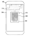
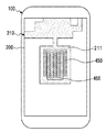
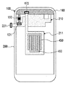
図2a、図2b及び図2cは、本発明の実施形態によるタッチ入力装置において、ディ
スプレイモジュールに対するタッチセンサパネルの相対的な位置を例示する概念図である
。図2aないし図2cにおいては、ディスプレイパネルとしてLCDパネルが示されてい
るが、これは例示に過ぎず、任意のディスプレイパネルが本発明の実施形態によるタッチ
入力装置1000に適用されてもよい。
2A, 2B, and 2C are conceptual views illustrating the relative position of the touch sensor panel with respect to the display module in the touch input device according to the embodiment of the present invention. 2a to 2c, an LCD panel is shown as a display panel. However, this is only an example, and any display panel may be applied to the
本願明細書において、図面符号200はディスプレイモジュールを指し示すが、図2及
びこれに対する説明において、図面符合200は、ディスプレイモジュールだけでなくデ
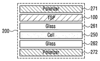
ィスプレイパネルを指し示してもよい。図2に示されたように、LCDパネルは、液晶セ
ル(liquid crystal cell)を含む液晶層250、液晶層250の両端
に電極を含む第1ガラス層261と第2ガラス層262、そして前記液晶層250と対向
する方向として前記第1ガラス層261の一面に第1偏光層271及び前記第2ガラス層
262の一面に第2偏光層272を含んでもよい。該当技術分野の当業者には、LCDパ
ネルがディスプレイ機能を遂行するために他の構成をさらに含んでもよく、変形が可能な
ことは自明であろう。
In the present specification, the
図2aは、タッチ入力装置1000において、タッチセンサパネル100がディスプレ
イモジュール200の外部に配置されたことを示す。タッチ入力装置1000に対するタ
ッチ表面は、タッチセンサパネル100の表面であってもよい。図2aにおいて、タッチ
表面になり得るタッチセンサパネル100の面は、タッチセンサパネル100の上部面に
なってもよい。また、実施形態によりタッチ入力装置1000に対するタッチ表面は、デ
ィスプレイモジュール200の外面になってもよい。図2aにおいて、タッチ表面になり
得るディスプレイモジュール200の外面は、ディスプレイモジュール200の第2偏光
層272の下部面になってもよい。この時、ディスプレイモジュール200を保護するた
めに、ディスプレイモジュール200の下部面はガラスのようなカバー層(図示せず)で
覆われていてもよい。
FIG. 2 a illustrates that the
図2b及び2cは、タッチ入力装置1000において、タッチセンサパネル100がデ
ィスプレイパネル200の内部に配置されたことを示す。この時、図2bにおいては、タ
ッチ位置を検出するためのタッチセンサパネル100が、第1ガラス層261と第1偏光
層271との間に配置されている。この時、タッチ入力装置1000に対するタッチ表面
は、ディスプレイモジュール200の外面として図2bで上部面又は下部面になってもよ
い。図2cにおいては、タッチ位置を検出するためのタッチセンサパネル100が、液晶
層250に含まれて具現される場合を例示する。この時、タッチ入力装置1000に対す
るタッチ表面は、ディスプレイモジュール200の外面として図2cで上部面又は下部面
になってもよい。図2b及び図2cにおいて、タッチ表面になり得るディスプレイモジュ
ール200の上部面又は下部面は、ガラスのようなカバー層(図示せず)で覆われていて
もよい。
FIGS. 2 b and 2 c show that the
以上においては、本発明の実施形態によるタッチセンサパネル100に対するタッチの
有無及び/又はタッチの位置を検出することを説明したが、本発明の実施形態によるタッ
チセンサパネル100を用いてタッチの有無及び/又は位置と共にタッチの圧力の大きさ
を検出することができる。また、タッチセンサパネル100と別個にタッチ圧力を検出す
る圧力検出モジュールをさらに含んで、タッチの圧力の大きさを検出することも可能であ
る。
In the above description, the presence / absence of touch and / or the position of the touch on the
図3は、本発明の第1実施形態により、タッチ位置及びタッチ圧力を検出できるように
構成されたタッチ入力装置の断面図である。
FIG. 3 is a cross-sectional view of a touch input device configured to detect a touch position and a touch pressure according to the first embodiment of the present invention.
ディスプレイモジュール200を含むタッチ入力装置1000において、タッチ位置を
検出するためのタッチセンサパネル100及び圧力検出モジュール400は、ディスプレ
イモジュール200の前面に付着されてもよい。これにより、ディスプレイモジュール2
00のディスプレイスクリーンを保護して、タッチセンサパネル100のタッチ検出の感
度を高めることができる。
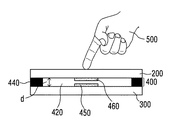
In the
The display screen of 00 can be protected and the sensitivity of touch detection of the
この時、圧力検出モジュール400は、タッチ位置を検出するためのタッチセンサパネ
ル100と別個に動作することもできるので、例えば、圧力検出モジュール400は、タ
ッチ位置を検出するためのタッチセンサパネル100と独立して圧力だけを検出するよう
に構成されてもよい。また、圧力検出モジュール400は、タッチ位置を検出するための
タッチセンサパネル100と結合してタッチ圧力を検出するように構成されてもよい。例
えば、タッチ位置を検出するためのタッチセンサパネル100に含まれた駆動電極TXと
受信電極RXのうち少なくとも一つの電極は、タッチ圧力を検出するのに用いられてもよ
い。
At this time, the
図3において、圧力検出モジュール400は、タッチセンサパネル100と結合してタ
ッチ圧力を検出できる場合を例示する。図3において、圧力検出モジュール400は、前
記タッチセンサパネル100とディスプレイモジュール200との間を離隔させるスペー
サ層420を含む。圧力検出モジュール400は、スペーサ層420を通じてタッチセン
サパネル100と離隔した基準電位層を含んでもよい。この時、ディスプレイモジュール
200は、基準電位層として機能することができる。
In FIG. 3, the
基準電位層は、駆動電極TXと受信電極RXとの間に生成された静電容量101に変化
を引き起こさせるようにする任意の電位を有してもよい。例えば、基準電位層は、グラン
ド(ground)電位を有するグランド層であってもよい。基準電位層は、ディスプレ
イモジュール200のグランド(ground)層であってもよい。この時、基準電位層
は、タッチセンサパネル100の2次元平面と平行した平面を有してもよい。
The reference potential layer may have an arbitrary potential that causes a change in the
図3に示されたように、タッチセンサパネル100と基準電位層であるディスプレイモ
ジュール200とは、離隔して位置する。この時、タッチセンサパネル100とディスプ
レイモジュール200の接着方法の差によって、タッチセンサパネル100とディスプレ
イモジュール200との間のスペーサ層420は、エアギャップ(air gap)で具
現されてもよい。
As shown in FIG. 3, the
この時、タッチセンサパネル100とディスプレイモジュール200とを固定するため
に、両面接着テープ430(DAT:Double Adhesive Tape)が用い
られてもよい。例えば、タッチセンサパネル100とディスプレイモジュール200は、
それぞれの面積が重ねられた形態であり、タッチセンサパネル100とディスプレイモジ
ュール200それぞれの端領域において両面接着テープ430を介して二つの層が接着さ
れるが、残りの領域においてタッチセンサパネル100とディスプレイモジュール200
とが所定の距離dに離隔されてもよい。
At this time, in order to fix the
The respective areas are overlapped, and two layers are bonded to each other in the end regions of the
May be separated by a predetermined distance d.
一般的に、タッチセンサパネル100の撓みなしにタッチ表面をタッチする場合でも、
駆動電極TXと受信電極RXとの間の静電容量101:Cmが変化する。すなわち、タッ
チセンサパネル100に対するタッチの際に、相互静電容量Cm:101が基本相互静電
容量に比べて減少する。これは指のような導体である客体がタッチセンサパネル100に
近接した場合、客体がグランドGNDの役割をして相互静電容量Cm:101のフリンジ
ング静電容量(fringing capacitance)が客体に吸収されるためで
ある。基本相互静電容量は、タッチセンサパネル100に対するタッチがない場合に、駆
動電極TXと受信電極RXとの間の相互静電容量の値である。
In general, even when the touch surface is touched without bending the
The capacitance 101: Cm between the drive electrode TX and the reception electrode RX changes. That is, when the
タッチセンサパネル100のタッチ表面である上部表面を客体でタッチする際に圧力が
加えられた場合、タッチセンサパネル100が撓む。この時、駆動電極TXと受信電極R
Xとの間の相互静電容量101:Cmの値はさらに減少する。これは、タッチセンサパネ
ル100が撓んでタッチセンサパネル100と基準電位層との間の距離がdからd’に減
少することによって、前記相互静電容量101:Cmのフリンジング静電容量が客体だけ
でなく基準電位層にも吸収されるためである。タッチの客体が不導体である場合には、相
互静電容量Cmの変化は、単にタッチセンサパネル100と基準電位層との間の距離変化
d−d’のみに起因してもよい。
When pressure is applied when the upper surface, which is the touch surface of the
The value of mutual capacitance 101: Cm with X further decreases. This is because the fringing capacitance of the mutual capacitance 101: Cm is changed to the object when the
以上で詳しく見たように、ディスプレイモジュール200上にタッチセンサパネル10
0及び圧力検出モジュール400を含んでタッチ入力装置1000を構成することによっ
て、タッチ位置だけでなくタッチ圧力を同時に検出することができる。
As detailed above, the touch sensor panel 10 is mounted on the
By configuring the
しかし、図3に示されたように、タッチセンサパネル100だけでなく圧力検出モジュ
ール400までディスプレイモジュール200の上部に配置させる場合、ディスプレイモ
ジュールのディスプレイ特性が低下する問題点が発生する。特に、ディスプレイモジュー
ル200の上部にエアギャップ420を含む場合に、ディスプレイモジュールの視認性及
び光透過率が低下することがある。
However, as shown in FIG. 3, when not only the
したがって、このような問題点が発生することを防止するために、タッチ位置を検出す
るためのタッチセンサパネル100とディスプレイモジュール200との間にエアギャッ
プを配置せずに、OCA(Optically Clear Adhesive)のような
接着剤でタッチセンサパネル100とディスプレイモジュール200とが完全ラミネーシ
ョン(lamination)されてもよい。
Accordingly, in order to prevent the occurrence of such a problem, an optical gap is not provided between the
図4は、本発明の第2実施形態によるタッチ入力装置の断面図である。本発明の第2実
施形態によるタッチ入力装置1000において、タッチ位置を検出するためのタッチセン
サパネル100とディスプレイモジュール200との間が接着剤で完全ラミネーションさ
れる。これによりタッチセンサパネル100のタッチ表面を通じて確認できるディスプレ
イモジュール200のディスプレイの色の鮮明度、視認性、及び光透過性が向上してもよ
い。
FIG. 4 is a cross-sectional view of a touch input device according to a second embodiment of the present invention. In the
図4及び図5、そしてこれを参照した説明において、本発明の第2実施形態によるタッ
チ入力装置1000として、タッチセンサパネル100がディスプレイモジュール200
上に接着剤でラミネーションされて付着したものを例示するが、本発明の第2実施形態に
よるタッチ入力装置1000は、タッチセンサパネル100が図2b及び図2cなどに示
されたように、ディスプレイモジュール200の内部に配置される場合も含んでいてもよ
い。より具体的に、図4及び図5において、タッチセンサパネル100がディスプレイモ
ジュール200を覆うことが示されているが、タッチセンサパネル100はディスプレイ
モジュール200の内部に位置して、ディスプレイモジュール200がガラスのようなカ
バー層で覆われたタッチ入力装置1000が、本発明の第2実施形態に用いられてもよい
。
4 and 5 and the description with reference thereto, the
The
本発明の実施形態によるタッチ入力装置1000は、携帯電話(cell phone
)、PDA(Personal Data Assistant)、スマートフォン(sm
artphone)、タブレットPC(taplet Personal Compute
r)、MP3プレーヤー、ノートブック(notebook)などのようなタッチスクリ
ーンを含む電子装置を含んでもよい。
A
), PDA (Personal Data Assistant), Smartphone (sm
artphone), tablet personal computer (tablet personal computer)
r), electronic devices including touch screens such as MP3 players, notebooks, etc.
本発明の実施形態によるタッチ入力装置1000において、基板300は、例えばタッ
チ入力装置1000の最外郭をなす機構であるカバー320と共にタッチ入力装置100
0の作動のための回路基板及び/又はバッテリーが位置することができる実装空間310
などを覆うハウジング(housing)の機能を遂行することができる。この時、タッ
チ入力装置1000の作動のための回路基板には、メインボード(main board
)として中央処理ユニットであるCPU(central processing uni
t)又はAP(application processor)などが実装されていても
よい。基板300を通じてディスプレイモジュール200とタッチ入力装置1000の作
動のための回路基板及び/又はバッテリーが分離し、ディスプレイモジュール200で発
生する電気的ノイズが遮断されてもよい。
In the
A mounting
The function of a housing for covering the like can be performed. At this time, a circuit board for operating the
) As a central processing unit CPU (central processing unit)
t) or AP (application processor) or the like may be implemented. A circuit board and / or a battery for operating the
タッチ入力装置1000において、タッチセンサパネル100又は前面カバー層が、デ
ィスプレイモジュール200、基板300、及び実装空間310より広く形成されてもよ
く、これによりカバー320がタッチセンサパネル100と共にディスプレイモジュール
200、基板300及び回路基板310を覆うように、カバー320が形成されてもよい
。
In the
本発明の第2実施形態によるタッチ入力装置1000は、タッチセンサパネル100を
通じてタッチ位置を検出し、ディスプレイモジュール200と基板300との間に圧力検
出モジュール400を配置してタッチ圧力を検出することができる。この時、タッチセン
サパネル100は、ディスプレイモジュール200の内部又は外部に位置することができ
る。圧力検出モジュール400は、例えば、エアギャップ(air gap)からなった
スペーサ層420を含んで構成され、これに対しては図5ないし図7bを参照して詳しく
見てみる。スペーサ層420は、実施形態により衝撃吸収物質からなってもよい。スペー
サ層420は、実施形態により誘電物質(dielectric material)で
満たされてもよい。
The
図5は、本発明の第2実施形態によるタッチ入力装置の斜視図である。図5に示された
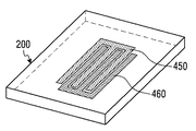
ように、本発明の実施形態によるタッチ入力装置1000において、圧力検出モジュール
400は、ディスプレイモジュール200と基板300を離隔させるスペーサ層420、
及びスペーサ層420内に位置する電極450及び460を含んでもよい。以下で、タッ
チセンサパネル100に含まれた電極と区分が明確なように、圧力を検出するための電極
450及び460を圧力電極450及び460と指称する。この時、圧力電極450及び
460は、ディスプレイパネルの前面でない後面に含まれるので、透明物質だけでなく不
透明物質で構成されることも可能である。
FIG. 5 is a perspective view of a touch input device according to a second embodiment of the present invention. As shown in FIG. 5, in the
And
この時、スペーサ層420を維持するために、基板300の上部の縁に沿って所定の厚
さを有する接着テープ440が形成されてもよい。図5において、接着テープ440は基
板300のすべての縁(例えば、四角形の4辺)に形成されたものが図示されているが、
接着テープ440は基板の縁のうち少なくとも一部(例えば、四角形の3辺)にのみ形成
されてもよい。実施形態により、接着テープ440は、基板300の上部面又はディスプ
レイモジュール200の下部面に形成されてもよい。接着テープ440は、基板300と
ディスプレイモジュール200を同一の電位に作るために伝導性テープであってもよい。
また、接着テープ440は、両面接着テープであってもよい。本発明の実施形態において
、接着テープ440は、弾性のない物質で構成されてもよい。本発明の実施形態において
、ディスプレイモジュール200に圧力が印加される場合、ディスプレイモジュール20
0が撓み得るので、接着テープ440が圧力によって形体の変形がなくても、タッチ圧力
の大きさを検出することができる。
At this time, an
The
The
Since 0 can bend, the magnitude of the touch pressure can be detected even if the
図6aは、本発明の第1実施形態による圧力電極パターンを含むタッチ入力装置の断面
図である。図6aに示されたように、本発明の第1実施形態による圧力電極450、46
0は、スペーサ層420内として基板300上に形成されてもよい。
FIG. 6a is a cross-sectional view of a touch input device including a pressure electrode pattern according to the first embodiment of the present invention. As shown in FIG. 6a, the
0 may be formed on the
圧力検出のための圧力電極は、第1電極450と第2電極460とを含んでもよい。こ
の時、第1電極450と第2電極460のうち、いずれか一つは駆動電極であってもよく
、残りの一つは受信電極であってもよい。駆動電極に駆動信号を印加して受信電極を通じ
て感知信号を獲得することができる。電圧が印加されると、第1電極450と第2電極4
60との間に相互静電容量が生成されてもよい。
The pressure electrode for pressure detection may include a
A mutual capacitance may be generated between 60 and 60.
図6bは、図6aに示されたタッチ入力装置1000に圧力が印加された場合の断面図
である。ディスプレイモジュール200の下部面は、ノイズ遮蔽のためにグランド(gr
ound)電位を有してもよい。客体500を通じてタッチセンサパネル100の表面に
圧力を印加する場合、タッチセンサパネル100及びディスプレイモジュール200は撓
み得る。これによりグランド電位面と圧力電極パターン450、460との間の距離dが
d’に減少する。このような場合、前記距離dの減少によりディスプレイモジュール20
0の下部面にフリンジング静電容量が吸収されるので、第1電極450と第2電極460
との間の相互静電容量は減少する。したがって、受信電極を通じて取得される感知信号に
おいて、相互静電容量の減少量を取得してタッチ圧力の大きさを算出することができる。
FIG. 6B is a cross-sectional view when a pressure is applied to the
ound) may have a potential. When pressure is applied to the surface of the
Since the fringing capacitance is absorbed by the lower surface of 0, the
The mutual capacitance between is reduced. Accordingly, it is possible to calculate the magnitude of the touch pressure by acquiring the reduction amount of the mutual capacitance in the sensing signal acquired through the receiving electrode.
本発明の実施形態によるタッチ入力装置1000において、ディスプレイモジュール2
00は、圧力を印加するタッチによって撓み得る。ディスプレイモジュール200は、タ
ッチの位置で最も大きい変形を示すように撓み得る。実施形態によりディスプレイモジュ
ール200が撓むとき、最も大きい変形を示す位置は、前記タッチ位置と一致しないこと
もあるが、ディスプレイモジュール200は、少なくとも前記タッチ位置で撓みを示すこ
とができる。例えば、タッチ位置がディスプレイモジュール200の縁や端などに近接す
る場合、ディスプレイモジュール200が撓む程度が最も大きい位置はタッチ位置と異な
ることもあるが、ディスプレイモジュール200は、少なくとも前記タッチ位置で撓みを
示すことができる。
In the
00 can bend by touch applying pressure. The
この時、基板300の上部面もまたノイズ遮蔽のためにグランド電位を有してもよい。
したがって、基板300と圧力電極450、460が短絡(short circuit
)することを防止するために、圧力電極450、460は絶縁層470上に形成されても
よい。図8は、本発明の実施形態による圧力電極の付着構造を例示する。図8(a)を参
照して説明すると、圧力電極450、460は、基板300上に第1絶縁層470を位置
させた後、圧力電極450、460を形成して構成されてもよい。また、実施形態により
圧力電極450、460が形成された第1絶縁層470を基板300上に付着して形成す
ることができる。また、実施形態により圧力電極は、基板300又は基板300上の第1
絶縁層470上に圧力電極パターンに相応する貫通孔を有するマスク(mask)を位置
させた後、伝導性スプレー(spray)を噴射することによって形成されてもよい。
At this time, the upper surface of the
Therefore, the
), The
A mask having a through hole corresponding to the pressure electrode pattern may be positioned on the insulating
また、ディスプレイモジュール200の下部面がグランド電位を有する場合、基板30
0上に位置した圧力電極450、460とディスプレイモジュール300とが短絡するの
を防止するために、圧力電極450、460は追加の第2絶縁層471で圧力電極450
、460を覆うことができる。また、第1絶縁層470上に形成された圧力電極450、
460を追加の第2絶縁層471で覆った後、一体型で基板300上に付着して圧力検出
モジュール400を形成することができる。
When the lower surface of the
In order to prevent the
460 can be covered. In addition, the
After the 460 is covered with the additional second insulating
図8(a)を参照して説明された圧力電極450、460の付着構造及び方法は、圧力
電極450、460がディスプレイモジュール200に付着する場合にも適用されてもよ
い。圧力電極450、460がディスプレイモジュール200に付着する場合は、図6c
と関連してさらに詳しく説明される。
The attachment structure and method of the
Will be described in more detail in connection with.
また、タッチ入力装置1000の種類及び/又は具現方式により、圧力電極450
、460が付着する基板300又はディスプレイモジュール200がグランド電位を示さ
ないか、もしくは弱いグランド電位を示してもよい。このような場合、本発明の実施形態
によるタッチ入力装置1000は、基板300又はディスプレイモジュール200と絶縁
層470との間にグランド電極(ground electrode:図示せず)をさら
に含んでもよい。実施形態により、グランド電極と基板300又はディスプレイモジュー
ル200との間には、また別の絶縁層(図示せず)をさらに含んでもよい。この時、グラ
ンド電極(図示せず)は、圧力電極である第1電極450と第2電極460との間に生成
される静電容量の大きさが非常に大きくなるのを防止することができる。
Further, the
The
以上で説明した圧力電極450、460の形成及び付着方法は、以下の実施形態にも同
様に適用されてもよい。
The method for forming and attaching the
図6cは、本発明の第2実施形態による圧力電極を含むタッチ入力装置の断面図で
ある。第1実施形態において、圧力電極450、460が基板300上に形成されたこと
が例示されているが、圧力電極450、460は、ディスプレイモジュール200の下部
面上に形成されても構わない。この時、基板300はグランド電位を有してもよい。した
がって、タッチセンサパネル100のタッチ表面をタッチすることにより、基板300と
圧力電極450、460との間の距離dが減少して、結果的に第1電極450と第2電極
460との間の相互静電容量の変化を引き起こすことができる。
FIG. 6c is a cross-sectional view of a touch input device including a pressure electrode according to a second embodiment of the present invention. In the first embodiment, it is exemplified that the
図6dは、本発明の第1実施形態による圧力電極パターンを例示する。図6dでは、第
1電極450と第2電極460とが基板300上に形成された場合を示す。第1電極45
0と第2電極460との間の静電容量は、ディスプレイモジュール200の下部面と圧力
電極450、460との間の距離によって変わり得る。
FIG. 6d illustrates a pressure electrode pattern according to the first embodiment of the present invention. FIG. 6 d shows a case where the
The capacitance between zero and the
図6eは、本発明の第2実施形態による圧力電極パターンを例示する。図6eにお
いて、圧力電極450、460は、ディスプレイモジュール200の下部面上に形成され
た場合を示す。
FIG. 6e illustrates a pressure electrode pattern according to a second embodiment of the present invention. In FIG. 6 e, the
図6f及び図6gは、本発明の実施形態に適用され得る圧力電極パターン450、
460を例示する。第1電極450と第2電極460との間の相互静電容量が変化するこ
とによってタッチ圧力の大きさを検出する時、検出の正確度を高めるために必要な静電容
量の範囲を生成するように、第1電極450と第2電極460のパターンを形成する必要
がある。第1電極450と第2電極460とが互いに向かい合う面積が大きいか、もしく
は長さが長いほど、生成される静電容量の大きさが大きくなってもよい。したがって、必
要な静電容量の範囲により、第1電極450と第2電極460との間の向かい合う面積の
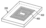
大きさ、長さ及び形状などを調節して設計することができる。図6f及び図6gには、第
1電極450と第2電極460とが同一の層に形成される場合として、第1電極450と
第2電極460とが互いに向かい合う長さが相対的に長いように圧力電極が形成された場
合を例示する。
6f and 6g illustrate a
460 is illustrated. When the magnitude of the touch pressure is detected by changing the mutual capacitance between the
第1実施形態と第2実施形態において、第1電極450と第2電極460は、同一
の層に形成されたもので示されているが、第1電極450と第2電極460は、実施形態
により互いに異なる層に具現されても構わない。図8(b)は、第1電極450と第2電
極460とが互いに異なる層に具現された場合の付着構造を例示する。図8(b)に例示
されたように、第1電極450は第1絶縁層470上に形成され、第2電極460は第1
電極450上に位置する第2絶縁層471上に形成されてもよい。実施形態により、第2
電極460は第3絶縁層472で覆われてもよい。この時、第1電極450と第2電極4
60とは互いに異なる層に位置するので、互いにオーバーラップ(overlap)する
ように具現されてもよい。例えば、第1電極450と第2電極460とは、図1を参照し
て説明されたタッチセンサパネル100に含まれたMXNの構造で配列された駆動電極T
Xと受信電極RXのパターンと類似するように形成されてもよい。この時、M及びNは、
1以上の自然数であってもよい。
In the first embodiment and the second embodiment, the
It may be formed on the second insulating
The
Since 60 is located in a different layer from each other, it may be implemented to overlap each other. For example, the
The pattern may be similar to the pattern of X and the receiving electrode RX. At this time, M and N are
It may be a natural number of 1 or more.
第1実施形態において、タッチ圧力は、第1電極450と第2電極460との間の相互
静電容量の変化から検出されることが例示される。しかし、圧力電極450、460が第
1電極450と第2電極460の何れか一つの圧力電極のみを含むように構成されてもよ
く、このような場合、一つの圧力電極とグランド層(ディスプレイモジュール200又は
基板300)との間の静電容量の変化を検出することによって、タッチ圧力の大きさを検
出することもできる。
In the first embodiment, it is exemplified that the touch pressure is detected from a change in mutual capacitance between the
例えば、図6aにおいて、圧力電極は第1電極450のみを含んで構成されてもよ
く、この時、ディスプレイモジュール200と第1電極450との間の距離変化によって
引き起こされる第1電極450とディスプレイモジュール200との間の静電容量の変化
からタッチ圧力の大きさを検出することができる。タッチ圧力が大きくなることによって
距離dが減少するので、ディスプレイモジュール200と第1電極450との間の静電容
量は、タッチ圧力が増加するほど大きくなり得る。これは、図6cと関連した実施形態に
も同様に適用されてもよい。この時、圧力電極は、相互静電容量の変化量の検出精度を高
めるために必要な、くし形状又はフォーク形状を有する必要はなく、図7bに例示された
ように、板(例えば、四角板)形状を有してもよい。
For example, in FIG. 6a, the pressure electrode may include only the
図8(c)は、圧力電極が第1電極450のみを含んで具現された場合の付着構造
を例示する。図8(c)に例示されたように、第1電極450は、基板300又はディス
プレイモジュール200上に位置した第1絶縁層470上に形成されてもよい。また、実
施形態により第1電極450は第2絶縁層471で覆われてもよい。
FIG. 8C illustrates an attachment structure when the pressure electrode is implemented to include only the
図7aは、本発明の第3実施形態による圧力電極を含むタッチ入力装置の断面図で
ある。本発明の第3実施形態による圧力電極450、460は、スペーサ層420内とし
て基板300の上部面及びディスプレイモジュール200の下部面上に形成されてもよい
。
FIG. 7a is a cross-sectional view of a touch input device including a pressure electrode according to a third embodiment of the present invention. The
圧力検出のための圧力電極パターンは、第1電極450と第2電極460を含んでもよ
い。この時、第1電極450と第2電極460の何れか一つは基板300上に形成され、
残りの一つはディスプレイモジュール200の下部面上に形成されてもよい。図7aにお
いては、第1電極450が基板300上に形成され、第2電極460がディスプレイモジ
ュール200の下部面上に形成されたことを例示する。
The pressure electrode pattern for pressure detection may include a
The remaining one may be formed on the lower surface of the
客体500を通じてタッチセンサパネル100の表面に圧力を印加する場合、タッ
チセンサパネル100及びディスプレイモジュール200は撓み得る。これにより第1電
極450及び第2電極460との間の距離dが減少する。このような場合、前記距離dの
減少により、第1電極450と第2電極460との間の相互静電容量は増加する。したが
って、受信電極を通じて取得される感知信号において、相互静電容量の減少量を取得して
タッチ圧力の大きさを算出することができる。
When pressure is applied to the surface of the
図7bは、本発明の第3実施形態による圧力電極パターンを例示する。図7bでは
、第1電極450が基板300の上部面上に形成され、第2電極460がディスプレイモ
ジュール200の下部面に形成されたことが示される。図7bに示されたように、第1電
極450と第2電極460とが互いに異なる層に形成されるので、第1実施形態と第2実
施形態とは異なり、第1電極450及び第2電極460は、くし形状又はフォーク形状を
有する必要はなく、板形状(例えば、四角板形状)を有してもよい。
FIG. 7b illustrates a pressure electrode pattern according to a third embodiment of the present invention. FIG. 7 b shows that the
図8(d)は、第1電極450が基板300上に付着し、第2電極460がディス
プレイモジュール200に付着した場合の付着構造を例示する。図8(d)に例示された
ように、第1電極450は、基板300上に形成された第1絶縁層470−2上に位置し
、第1電極450は第2絶縁層471−2によって覆われていてもよい。また、第2電極
460はディスプレイモジュール200の下部面上に形成された第1絶縁層470−1上
に位置し、第2電極460は第2絶縁層471−1によって覆われていてもよい。
FIG. 8D illustrates an attachment structure when the
図8(a)と関連して説明されたことと同様に、圧力電極450、460が付着す
る基板300又はディスプレイモジュール200がグランド電位を示さないか、もしくは
弱いグランド電位を示す場合、図8(a)ないし図8(d)において第1絶縁層470、
470−1、470−2の間にグランド電極(図示せず)をさらに含んでもよい。この時
、グランド電極(図示せず)と圧力電極450、460が付着する基板300又はディス
プレイモジュール200の間には、追加の絶縁層(図示せず)をさらに含んでもよい。
Similar to that described in connection with FIG. 8A, when the
A ground electrode (not shown) may be further included between 470-1 and 470-2. At this time, an additional insulating layer (not shown) may be further included between the ground electrode (not shown) and the
以上で詳しく見たように、本発明の実施形態によるタッチ入力装置1000は、圧
力電極450、460で発生する静電容量の変化を感知する。したがって、第1電極45
0と第2電極460のうち駆動電極には駆動信号が印加される必要があり、受信電極から
感知信号を取得して静電容量の変化量からタッチ圧力を算出しなければならない。実施形
態により、圧力検出モジュール400の動作のためのタッチセンシングICを追加で含む
ことも可能である。このような場合、図1に示されたように、駆動部120、感知部11
0、及び制御部130と類似した構成を重複して含むようになるので、タッチ入力装置1
000の面積及び体積が大きくなる問題点が発生し得る。
As described above in detail, the
A driving signal needs to be applied to the driving electrode among 0 and the
0 and the configuration similar to the
The problem that the area and volume of 000 become large may occur.
実施形態により、圧力検出モジュール400は、タッチセンサパネル100の作動のた
めのタッチ検出装置を通じて駆動信号が印加され、感知信号の入力を受けてタッチ圧力を
検出することができる。以下では、第1電極450が駆動電極であり、第2電極460が
受信電極である場合を仮定して説明する。
According to the embodiment, the
このために、本発明の実施形態によるタッチ入力装置1000において、第1電極
450は駆動部120から駆動信号の印加を受け、第2電極460は感知信号を感知部1
10に伝達することができる。制御部130は、タッチセンサパネル100のスキャニン
グを遂行すると共に圧力検出モジュール400のスキャニングを遂行するようにしたり、
又は、制御部130は時分割して第1時間区間にはタッチセンサパネル100のスキャニ
ングを遂行するようにし、第1時間区間とは異なる第2時間区間には圧力検出モジュール
400のスキャニングを遂行するように制御信号を生成することができる。
For this, in the
10 can be transmitted. The
Alternatively, the
したがって、本発明の実施形態において、第1電極450と第2電極460は、電
気的に駆動部120及び/又は感知部110に連結されなければならない。この時、タッ
チセンサパネル100のためのタッチ検出装置は、タッチセンシングIC150としてタ
ッチセンサパネル100の一端、又は、タッチセンサパネル100と同一の平面上に形成
されることが一般的である。圧力電極パターン450、460は、任意の方法でタッチセ
ンサパネル100のタッチ検出装置と電気的に連結されてもよい。例えば、圧力電極パタ
ーン450、460は、ディスプレイモジュール200に含まれた第2PCB210を用
いてコネクタ(connector)を通じてタッチ検出装置に連結されてもよい。例え
ば、図5に示されたように、第1電極450と第2電極460からそれぞれ電気的に延び
る伝導性トレース451及び461は、第2PCB210などを通じてタッチセンシング
IC150まで電気的に連結されてもよい。
Accordingly, in the embodiment of the present invention, the
図9a及び図9bは、本発明の第2実施形態による圧力電極の付着方法を例示する。
図9a及び図9bでは、本発明の実施形態による圧力電極450、460がディスプレイ
モジュール200の下部面に付着される場合を示す。図9a及び図9bにおいて、ディス
プレイモジュール200は、下部面の一部にディスプレイパネルの作動のための回路が実
装された第2PCB210が示される。
9a and 9b illustrate a pressure electrode deposition method according to a second embodiment of the present invention.
9A and 9B illustrate the case where the
図9aは、第1電極450と第2電極460がディスプレイモジュール200の第2P
CB210の一端に連結されるように、圧力電極450、460をディスプレイモジュー
ル200の下部面に付着する場合を例示する。この時、図9aにおいては、第1電極45
0と第2電極460が絶縁層470上に製作された場合を例示する。圧力電極450、4
60は絶縁層470上に形成され、一体型シート(sheet)としてディスプレイモジ
ュール200の下部面に付着されてもよい。第2PCB210上には、圧力電極パターン
450、460をタッチセンシングIC150などの必要な構成まで電気的に連結できる
ように導電性パターンが印刷されていてもよい。これに対する詳細な説明は、図10aな
いし図10cを参照して説明する。
FIG. 9 a shows that the
The case where the
The case where 0 and the
60 may be formed on the insulating
図9bは、第1電極450と第2電極460がディスプレイモジュール200の第2
PCB210に一体型で形成された場合を例示する。例えば、ディスプレイモジュール2
00の第2PCB210の製作時に、第2PCBに一定の面積211を割愛して予めディ
スプレイパネルの作動のための回路だけでなく、第1電極450と第2電極460に該当
するパターンまで印刷することができる。第2PCB210には、第1電極450及び第
2電極460をタッチセンシングIC150などの必要な構成まで電気的に連結する導電
性パターンが印刷されてもよい。
FIG. 9 b shows that the
The case where it forms integrally with PCB210 is illustrated. For example,
When the 00
図10aないし図10cは、本発明の第2実施形態による圧力電極をタッチセンシン
グIC150に連結する方法を例示する。図10aないし図10cにおいて、タッチセン
サパネル100がディスプレイモジュール200の外部に含まれた場合として、タッチセ
ンサパネル100のタッチ検出装置がタッチセンサパネル100のための第1PCB16
0に実装されたタッチセンシングIC150に集積された場合を例示する。
FIGS. 10 a to 10 c illustrate a method of connecting a pressure electrode to the
The case where it is integrated in the
図10aにおいて、ディスプレイモジュール200に付着された圧力電極450、
460が、第1コネクタ121を通じてタッチセンシングIC150まで連結される場合
を例示する。図10aに例示されたように、スマートフォンのような移動通信装置におい
てタッチセンシングIC150は、第1コネクタ(connector)121を通じて
ディスプレイモジュール200のための第2PCB210に連結される。第2PCB21
0は、第2コネクタ221を通じてメインボードに電気的に連結されてもよい。したがっ
て、タッチセンシングIC150は、第1コネクタ121及び第2コネクタ221を通じ
てタッチ入力装置1000の作動のためにCPU又はAPと信号をやり取りすることがで
きる。
In FIG. 10a, a
The case where 460 is connected to the
0 may be electrically connected to the main board through the
この時、図10aにおいては、圧力電極450が図9bに例示されたような方式でデ
ィスプレイモジュール200に付着されたことが例示されているが、図9aに例示された
ような方式で付着した場合にも適用されてもよい。第2PCB210には、圧力電極45
0、460が第1コネクタ121を通じてタッチセンシングIC150まで電気的に連結
され得るように導電性パターンが印刷されていてもよい。
At this time, in FIG. 10a, it is illustrated that the
A conductive pattern may be printed so that 0 and 460 can be electrically connected to the
図10bにおいて、ディスプレイモジュール200に付着された圧力電極450、
460が、第3コネクタ471を通じてタッチセンシングIC150まで連結される場合
が例示される。図10bにおいて、圧力電極450、460は、第3コネクタ471を通
じてタッチ入力装置1000の作動のためのメインボードまで連結され、その後、第2コ
ネクタ221及び第1コネクタ121を通じてタッチセンシングIC150まで連結され
てもよい。この時、圧力電極450、460は、第2PCB210と分離した追加のPC
B211上に印刷されてもよい。または、実施形態により圧力電極パターン450、46
0は絶縁層470上に形成され、圧力電極450、460から伝導性トレースなどを延長
させてコネクタ471を通じてメインボードまで連結されてもよい。
In FIG. 10b, the
The case where 460 is connected to the
It may be printed on B211. Alternatively, the
0 may be formed on the insulating
図10cにおいて、圧力電極450、460が第4コネクタ472を通じて直接タッチ
センシングIC150に連結される場合が例示される。図10cにおいて、圧力電極45
0、460は、第4コネクタ472を通じて第1PCB160まで連結されてもよい。第
1PCB160には、第4コネクタ472からタッチセンシングIC150まで電気的に
連結する導電性パターンが印刷されていてもよい。これにより、圧力電極450、460
は、第4コネクタ472を通じてタッチセンシングIC150まで連結されてもよい。こ
の時、圧力電極450、460は、第2PCB210と分離した追加のPCB211上に
印刷されてもよい。第2PCB210と追加のPCB211は、互いに短絡しないように
絶縁されていてもよい。または、実施形態により圧力電極450、460は絶縁層470
上に形成され、圧力電極450、460から伝導性トレースなどを延長させてコネクタ4
72を通じて第1PCB160まで連結されてもよい。
FIG. 10 c illustrates a case where the
0 and 460 may be connected to the
May be connected to the
The connector 4 is formed by extending a conductive trace or the like from the
72 to the
図10b及び図10cの連結方法は、圧力電極450、460がディスプレイモジ
ュール200の下部面だけでなく、基板300上に形成された場合にも適用されてもよい
。
10b and 10c may be applied to the case where the
図10aないし図10cにおいては、タッチセンシングIC150が第1PCB16
0上に形成されたCOF(chip on film)構造を仮定して説明された。しかし
、これは単に例示に過ぎず、本発明は、タッチセンシングIC150がタッチ入力装置1
000の実装空間310内のメインボード上に実装されるCOB(chip on boa
rd)構造の場合にも適用されてもよい。図10aないし図10cに対する説明から、当
該技術分野の当業者に、他の実施形態の場合に圧力電極450、460のコネクタを通じ
た連結は自明であろう。
10A to 10C, the
The description has been made assuming a COF (chip on film) structure formed on zero. However, this is merely an example, and in the present invention, the
COB (chip on boa) mounted on the main board in the mounting
It may also be applied to the case of the rd) structure. From the description of FIGS. 10a to 10c, it will be apparent to those skilled in the art that the
以上においては、駆動電極として第1電極450が一つのチャネルを構成し、受信電
極として第2電極460が一つのチャネルを構成する圧力電極450、460に対して詳
しく見てみた。しかし、これは単に例示に過ぎず、実施形態により駆動電極及び受信電極
は、それぞれ複数個のチャネルを構成して多重タッチ(multi touch)によっ
て多重の圧力検出が可能であり得る。
In the above, the
図11aないし図11cは、本発明の実施形態による圧力電極が複数のチャネルを構
成する場合を例示する。図11aでは、第1電極450−1、450−2と第2電極46
0−1、460−2それぞれが2個のチャネルを構成する場合が例示される。図11bで
は、第1電極450は2個のチャネル450−1、450−2を構成するが、第2電極4
60は1個のチャネルを構成する場合が例示される。図11cでは、第1電極450−1
ないし450−5と第2電極460−1、460−5それぞれが5個のチャネルを構成す
る場合が例示される。
FIGS. 11 a to 11 c illustrate the case where the pressure electrode according to the embodiment of the present invention constitutes a plurality of channels. In FIG. 11a, the first electrodes 450-1, 450-2 and the second electrode 46.
The case where each of 0-1 and 460-2 configures two channels is illustrated. In FIG. 11b, the
A case where 60 constitutes one channel is exemplified. In FIG. 11c, the first electrode 450-1
In addition, a case where each of 450-5 and the second electrodes 460-1, 460-5 constitute five channels is illustrated.
図11aないし図11cは、圧力電極が単数又は複数のチャネルを構成する場合を例
示して、多様な方法で圧力電極が単数又は複数のチャネルで構成されてもよい。図11a
ないし図11cにおいて、圧力電極450、460がタッチセンシングIC150に電気
的に連結される場合が例示されなかったが、図10aないし図10c及びその他の方法で
圧力電極450、460がタッチセンシングIC150に連結されてもよい。
FIGS. 11a to 11c illustrate the case where the pressure electrode constitutes one or more channels, and the pressure electrode may be comprised of one or more channels in various ways. FIG.
11C, the case where the
図12は、本発明の実施形態によるタッチ入力装置1000のタッチ表面中心部を
非伝導性客体で加圧する実験を遂行し、客体のグラム重量(gram force)に伴
う静電容量の変化量を表示するグラフである。図12から分かるように、本発明の実施形
態によるタッチ入力装置1000のタッチ表面中心部を加圧する力が大きくなるほど、圧
力検出モジュール400に含まれた圧力電極パターン450、460の静電容量の変化量
が大きくなることが分かる。
FIG. 12 illustrates an experiment in which the center part of the touch surface of the
以上においては、圧力検出モジュール400として静電容量方式の検出モジュールが説
明されたが、本発明の実施形態によるタッチ入力装置1000は、圧力検出モジュール4
00としてスペーサ層420及び圧力電極450、460を用いる場合であれば、任意の
方式の圧力検出モジュールを用いることができる。
In the above description, the capacitance type detection module has been described as the
If the
以上において実施形態に説明された特徴、構造、効果などは、本発明の一つの実施形態
に含まれ、必ずしも一つの実施形態にのみ限定される訳ではなく、さらに、各実施形態に
おいて例示された特徴、構造、効果などは、実施形態が属する分野における通常の知識を
有する者によって他の実施形態に対しても組み合わせ、又は変形されて実施可能である。
したがって、このような組み合わせと変形に関係した内容は、本発明の範囲に含まれるも
のと解釈されなければならないだろう。
The features, structures, effects, and the like described in the above embodiments are included in one embodiment of the present invention and are not necessarily limited to only one embodiment, and are further exemplified in each embodiment. Features, structures, effects, and the like can be implemented by combining or modifying other embodiments by those having ordinary knowledge in the field to which the embodiments belong.
Accordingly, contents related to such combinations and modifications should be construed as being included in the scope of the present invention.
また、以上において、実施形態を中心に説明したが、これは単に例示に過ぎず、本発明
を限定する訳ではなく、本発明が属する分野における通常の知識を有する者であれば、本
実施形態の本質的な特徴を外れない範囲で、以上に例示されない様々な変形と応用が可能
であることが分かるはずである。例えば、実施形態に具体的に示された各構成要素は、変
形して実施することができるものである。そして、このような変形と応用に係る相違点は
、添付の特許請求の範囲において規定する本発明の範囲に含まれるものと解釈されるべき
である。
In the above description, the embodiment has been mainly described. However, this is merely an example, and does not limit the present invention. Any person having ordinary knowledge in the field to which the present invention belongs will be described. It should be understood that various modifications and applications not exemplified above are possible without departing from the essential characteristics of the above. For example, each component specifically shown in the embodiment can be modified and implemented. Such differences in modification and application should be construed as being included in the scope of the present invention as defined in the appended claims.
1000 タッチ入力装置
100 タッチセンサパネル
110 感知部
120 駆動部
130 制御部
200 ディスプレイモジュール
300 基板
400 圧力検出モジュール
420 スペーサ層
450、460 電極
1000
Claims (13)
ディスプレイパネルを含むディスプレイモジュールと、
前記ディスプレイモジュールの下部に配置され、スペーサ層によって離隔された基板と
、
前記ディスプレイモジュールに直接形成された圧力電極と、
を含み、
前記圧力電極から前記圧力電極と前記基板との間の静電容量によって変化する電気的信
号が検出され、
前記静電容量は、前記圧力電極と前記基板との間の相対的な距離変化によって変わり、
前記静電容量に基づいて前記タッチの圧力を検出する、
タッチ入力装置。 A touch input device capable of detecting a pressure of a touch on a touch surface,
A display module including a display panel;
A substrate disposed under the display module and separated by a spacer layer;
A pressure electrode formed directly on the display module;
Including
An electrical signal that varies depending on the capacitance between the pressure electrode and the substrate is detected from the pressure electrode;
The capacitance is changed by a relative distance change between the pressure electrode and the substrate,
Detecting the pressure of the touch based on the capacitance;
Touch input device.
載のタッチ入力装置。 The touch input device according to claim 1, wherein the pressure electrode is directly formed on a lower surface of the display module.
ディスプレイパネルを含むディスプレイモジュールと、
前記ディスプレイモジュールの下部に配置され、スペーサ層によって離隔された基板と
、
前記ディスプレイモジュールに一体型で形成された圧力電極と、
を含み、
前記圧力電極から前記圧力電極と前記基板との間の静電容量によって変化する電気的信
号が検出され、
前記静電容量は、前記圧力電極と前記基板との間の相対的な距離変化によって変わり、
前記静電容量に基づいて前記タッチの圧力を検出する、
タッチ入力装置。 A touch input device capable of detecting a pressure of a touch on a touch surface,
A display module including a display panel;
A substrate disposed under the display module and separated by a spacer layer;
A pressure electrode formed integrally with the display module;
Including
An electrical signal that varies depending on the capacitance between the pressure electrode and the substrate is detected from the pressure electrode;
The capacitance is changed by a relative distance change between the pressure electrode and the substrate,
Detecting the pressure of the touch based on the capacitance;
Touch input device.
に記載のタッチ入力装置。 The pressure electrode is integrally formed on a lower surface of the display module.
The touch input device according to 1.
ディスプレイパネルを含むディスプレイモジュールと、
前記ディスプレイモジュールの下部に配置され、スペーサ層によって離隔された基板と
、
前記ディスプレイモジュールに印刷された圧力電極と、
を含み、
前記圧力電極から前記圧力電極と前記基板との間の静電容量によって変化する電気的信
号が検出され、
前記静電容量は、前記圧力電極と前記基板との間の相対的な距離変化によって変わり、
前記静電容量に基づいて前記タッチの圧力を検出する、
タッチ入力装置。 A touch input device capable of detecting a pressure of a touch on a touch surface,
A display module including a display panel;
A substrate disposed under the display module and separated by a spacer layer;
A pressure electrode printed on the display module;
Including
An electrical signal that varies depending on the capacitance between the pressure electrode and the substrate is detected from the pressure electrode;
The capacitance is changed by a relative distance change between the pressure electrode and the substrate,
Detecting the pressure of the touch based on the capacitance;
Touch input device.
タッチ入力装置。 The touch input device according to claim 5, wherein the pressure electrode is printed on a lower surface of the display module.
ディスプレイパネルを含むディスプレイモジュールと、
前記ディスプレイモジュールの下部に配置され、スペーサ層によって離隔された基板と
、
前記ディスプレイモジュールにパターン化された圧力電極と、
を含み、
前記圧力電極から前記圧力電極と前記基板との間の静電容量によって変化する電気的信
号が検出され、
前記静電容量は、前記圧力電極と前記基板との間の相対的な距離変化によって変わり、
前記静電容量に基づいて前記タッチの圧力を検出する、
タッチ入力装置。 A touch input device capable of detecting a pressure of a touch on a touch surface,
A display module including a display panel;
A substrate disposed under the display module and separated by a spacer layer;
A pressure electrode patterned on the display module;
Including
An electrical signal that varies depending on the capacitance between the pressure electrode and the substrate is detected from the pressure electrode;
The capacitance is changed by a relative distance change between the pressure electrode and the substrate,
Detecting the pressure of the touch based on the capacitance;
Touch input device.
に記載のタッチ入力装置。 The pressure electrode is printed as a pattern on the display module.
The touch input device according to 1.
求項8に記載のタッチ入力装置。 The touch input device according to claim 8, wherein the pressure electrode is printed as a pattern on a lower surface of the display module.
)を位置させた後、伝導性スプレーを噴射することによって形成される、請求項1ないし
9のいずれか1項に記載のタッチ入力装置。 The pressure electrode includes a mask having a through hole corresponding to a pattern of the pressure electrode.
10. The touch input device according to claim 1, wherein the touch input device is formed by spraying a conductive spray after positioning.
前記ディスプレイモジュールが撓むことによって前記圧力電極と前記基板との間の距離
が変わる、請求項1ないし10のいずれか1項に記載のタッチ入力装置。 If the pressure is applied, the display module bends,
The touch input device according to claim 1, wherein a distance between the pressure electrode and the substrate is changed by bending the display module.
載のタッチ入力装置。 The touch input device according to claim 1, wherein the pressure electrode forms a plurality of channels.
2に記載のタッチ入力装置。 The multiple pressure detection for multiple touches is possible using the plurality of channels.
3. The touch input device according to 2.
Applications Claiming Priority (2)
| Application Number | Priority Date | Filing Date | Title |
|---|---|---|---|
| KR1020140098917A KR101681305B1 (en) | 2014-08-01 | 2014-08-01 | Touch input device |
| KR10-2014-0098917 | 2014-08-01 |
Related Parent Applications (1)
| Application Number | Title | Priority Date | Filing Date |
|---|---|---|---|
| JP2016014898A Division JP6163218B2 (en) | 2014-08-01 | 2016-01-28 | smartphone |
Publications (3)
| Publication Number | Publication Date |
|---|---|
| JP2017117490A true JP2017117490A (en) | 2017-06-29 |
| JP2017117490A5 JP2017117490A5 (en) | 2018-08-02 |
| JP7198469B2 JP7198469B2 (en) | 2023-01-04 |
Family
ID=55180644
Family Applications (5)
| Application Number | Title | Priority Date | Filing Date |
|---|---|---|---|
| JP2015124247A Active JP6145134B2 (en) | 2014-08-01 | 2015-06-19 | smartphone |
| JP2015219873A Active JP6262703B2 (en) | 2014-08-01 | 2015-11-09 | smartphone |
| JP2016012175A Pending JP2016105304A (en) | 2014-08-01 | 2016-01-26 | smartphone |
| JP2016014898A Active JP6163218B2 (en) | 2014-08-01 | 2016-01-28 | smartphone |
| JP2017036310A Active JP7198469B2 (en) | 2014-08-01 | 2017-02-28 | smartphone |
Family Applications Before (4)
| Application Number | Title | Priority Date | Filing Date |
|---|---|---|---|
| JP2015124247A Active JP6145134B2 (en) | 2014-08-01 | 2015-06-19 | smartphone |
| JP2015219873A Active JP6262703B2 (en) | 2014-08-01 | 2015-11-09 | smartphone |
| JP2016012175A Pending JP2016105304A (en) | 2014-08-01 | 2016-01-26 | smartphone |
| JP2016014898A Active JP6163218B2 (en) | 2014-08-01 | 2016-01-28 | smartphone |
Country Status (6)
| Country | Link |
|---|---|
| US (5) | US10133377B2 (en) |
| EP (3) | EP3059666B1 (en) |
| JP (5) | JP6145134B2 (en) |
| KR (1) | KR101681305B1 (en) |
| CN (2) | CN207198825U (en) |
| WO (1) | WO2016018126A1 (en) |
Families Citing this family (63)
| Publication number | Priority date | Publication date | Assignee | Title |
|---|---|---|---|---|
| WO2013165601A1 (en) | 2012-05-03 | 2013-11-07 | Yknots Industries Llc | Moment compensated bending beam sensor for load measurement on platform supported by bending beams |
| US9983715B2 (en) | 2012-12-17 | 2018-05-29 | Apple Inc. | Force detection in touch devices using piezoelectric sensors |
| WO2014149023A1 (en) | 2013-03-15 | 2014-09-25 | Rinand Solutions Llc | Force sensing of inputs through strain analysis |
| KR101452302B1 (en) | 2013-07-29 | 2014-10-22 | 주식회사 하이딥 | Touch sensor panel |
| KR101681305B1 (en) | 2014-08-01 | 2016-12-02 | 주식회사 하이딥 | Touch input device |
| US10007380B2 (en) | 2013-07-29 | 2018-06-26 | Hideep Inc. | Touch input device with edge support member |
| CN110134283B (en) | 2013-10-28 | 2022-10-11 | 苹果公司 | Piezoelectric based force sensing |
| KR101712346B1 (en) | 2014-09-19 | 2017-03-22 | 주식회사 하이딥 | Touch input device |
| AU2015100011B4 (en) | 2014-01-13 | 2015-07-16 | Apple Inc. | Temperature compensating transparent force sensor |
| JP6527343B2 (en) | 2014-08-01 | 2019-06-05 | 株式会社 ハイディープHiDeep Inc. | Touch input device |
| JP5845371B1 (en) | 2014-09-19 | 2016-01-20 | 株式会社 ハイディープ | smartphone |
| KR20160068439A (en) * | 2014-12-05 | 2016-06-15 | 삼성전자주식회사 | Hybrid touch based electronic appatatus and controlling method thereof |
| US9612170B2 (en) | 2015-07-21 | 2017-04-04 | Apple Inc. | Transparent strain sensors in an electronic device |
| KR101583765B1 (en) | 2015-07-27 | 2016-01-08 | 주식회사 하이딥 | Smartphone |
| US10055048B2 (en) | 2015-07-31 | 2018-08-21 | Apple Inc. | Noise adaptive force touch |
| US9874965B2 (en) | 2015-09-11 | 2018-01-23 | Apple Inc. | Transparent strain sensors in an electronic device |
| US9886118B2 (en) | 2015-09-30 | 2018-02-06 | Apple Inc. | Transparent force sensitive structures in an electronic device |
| US10006820B2 (en) | 2016-03-08 | 2018-06-26 | Apple Inc. | Magnetic interference avoidance in resistive sensors |
| JP6297613B2 (en) * | 2016-03-22 | 2018-03-20 | Nissha株式会社 | Pressure sensor |
| JP6700896B2 (en) * | 2016-03-25 | 2020-05-27 | 株式会社ジャパンディスプレイ | Detection device and display device with touch detection function |
| WO2017170131A1 (en) * | 2016-03-28 | 2017-10-05 | シャープ株式会社 | Display panel fitted with pressure sensor |
| US10209830B2 (en) * | 2016-03-31 | 2019-02-19 | Apple Inc. | Electronic device having direction-dependent strain elements |
| CN108885506B (en) * | 2016-04-05 | 2022-03-01 | 希迪普公司 | Pressure sensor, touch input device including the same, and pressure detection method using the same |
| JP6671461B2 (en) * | 2016-04-08 | 2020-03-25 | 株式会社 ハイディープHiDeep Inc. | Pressure sensor constituting a plurality of channels, touch input device including the same, and pressure detection method using the same |
| EP3457258B1 (en) | 2016-06-15 | 2021-07-28 | Shenzhen Goodix Technology Co., Ltd. | Pressure detection apparatus and method, touch control device and electronic terminal |
| EP3293617B1 (en) * | 2016-06-16 | 2020-01-29 | Shenzhen Goodix Technology Co., Ltd. | Touch sensor, touch detection apparatus and detection method, and touch control device |
| KR102555596B1 (en) * | 2016-06-21 | 2023-07-17 | 삼성디스플레이 주식회사 | Electronic apparatus |
| KR102542992B1 (en) * | 2016-07-14 | 2023-06-15 | 삼성디스플레이 주식회사 | Touch sensor and display device having the same |
| KR102552283B1 (en) * | 2016-07-15 | 2023-07-10 | 삼성디스플레이 주식회사 | Pressure sensor and display device including the same |
| KR102531168B1 (en) * | 2016-07-26 | 2023-05-12 | 삼성디스플레이 주식회사 | Display apparatus |
| KR102562612B1 (en) | 2016-08-05 | 2023-08-03 | 삼성전자주식회사 | Electronic Device for Including Display Equipped with Force Sensor |
| KR102589636B1 (en) * | 2016-08-05 | 2023-10-17 | 삼성전자주식회사 | electronic device including fingerprint sensor |
| US10133418B2 (en) * | 2016-09-07 | 2018-11-20 | Apple Inc. | Force sensing in an electronic device using a single layer of strain-sensitive structures |
| KR102373566B1 (en) | 2016-09-23 | 2022-03-14 | 삼성디스플레이 주식회사 | Display device |
| KR101956295B1 (en) | 2016-11-22 | 2019-03-08 | 주식회사 하이딥 | Touch input device |
| US11561636B2 (en) * | 2016-11-24 | 2023-01-24 | Hideep Inc. | Touch input device for detecting pressure with display noise compensation |
| KR101908463B1 (en) * | 2017-02-16 | 2018-10-17 | 주식회사 하이딥 | Touch input device |
| US11221705B2 (en) | 2017-03-15 | 2022-01-11 | Mitsubishi Electric Corporation | Touch panel and display device including a pressure-sensitive sensor |
| DE112018001389T5 (en) * | 2017-03-15 | 2019-11-28 | Mitsubishi Electric Corporation | Touchpanel and display device equipped with one |
| US11487390B2 (en) | 2017-03-28 | 2022-11-01 | Sony Corporation | Information processing apparatus and control method of information processing apparatus |
| US11086464B2 (en) * | 2017-03-29 | 2021-08-10 | Sharp Kabushiki Kaisha | Display device with touch panel providing touched position detection and pressing force detection |
| US10444091B2 (en) | 2017-04-11 | 2019-10-15 | Apple Inc. | Row column architecture for strain sensing |
| KR101939280B1 (en) * | 2017-05-19 | 2019-01-18 | 주식회사 시노펙스 | Capacitive force sensor switch |
| US10309846B2 (en) | 2017-07-24 | 2019-06-04 | Apple Inc. | Magnetic field cancellation for strain sensors |
| CN207068439U (en) * | 2017-08-16 | 2018-03-02 | 京东方科技集团股份有限公司 | Lighting machine |
| KR102405666B1 (en) * | 2017-08-18 | 2022-06-07 | 삼성전자주식회사 | Electronic apparatus and method for controlling touch sensing signals and storage medium |
| CN107608559B (en) * | 2017-10-16 | 2021-03-02 | 京东方科技集团股份有限公司 | Force sensing unit, preparation method thereof, touch panel and touch display panel |
| KR102545479B1 (en) * | 2018-07-31 | 2023-06-20 | 삼성디스플레이 주식회사 | Display device |
| KR102550324B1 (en) | 2018-08-01 | 2023-07-03 | 삼성디스플레이 주식회사 | Display device |
| KR102626021B1 (en) * | 2018-08-14 | 2024-01-17 | 삼성디스플레이 주식회사 | Display device |
| US10782818B2 (en) | 2018-08-29 | 2020-09-22 | Apple Inc. | Load cell array for detection of force input to an electronic device enclosure |
| KR102018155B1 (en) * | 2018-10-10 | 2019-09-04 | 주식회사 하이딥 | Touch input device |
| KR102151986B1 (en) * | 2018-11-16 | 2020-09-04 | 한국과학기술원 | Touch input apparatus and method for manufacturing the touch input apparatus |
| KR102145567B1 (en) * | 2018-11-29 | 2020-08-18 | 한국과학기술원 | Touch input apparatus, grating substrate for the touch input apparatus, and grating substrate manufacturing method for the touch input apparatus |
| KR102233459B1 (en) * | 2019-01-22 | 2021-03-29 | 한국과학기술원 | Touch input apparatus and touch input apparatus manufacturing method |
| KR102650383B1 (en) | 2019-03-26 | 2024-03-25 | 삼성디스플레이 주식회사 | Electronic apparatus and method of driving the same |
| US11275460B2 (en) * | 2019-04-26 | 2022-03-15 | Samsung Display Co., Ltd. | Display device |
| KR20200143609A (en) | 2019-06-14 | 2020-12-24 | 삼성디스플레이 주식회사 | Display module and display display device having the same |
| KR102437876B1 (en) * | 2019-06-28 | 2022-09-01 | (주)아이테드 | Electronic device having the transparent heating module |
| KR102234090B1 (en) * | 2019-06-28 | 2021-03-31 | (주)아이테드 | Electronic device having the transparent heating module |
| KR102330801B1 (en) | 2019-12-31 | 2021-11-25 | 한국과학기술원 | Touch input apparatus |
| JP7321112B2 (en) * | 2020-02-10 | 2023-08-04 | 三菱電機株式会社 | Touch panel and display device provided with the same |
| US11726597B1 (en) | 2022-05-27 | 2023-08-15 | Microsoft Technology Licensing, Llc | Differential capacitive force sensing |
Citations (15)
| Publication number | Priority date | Publication date | Assignee | Title |
|---|---|---|---|---|
| WO2011013588A1 (en) * | 2009-07-29 | 2011-02-03 | アルプス電気株式会社 | Manipulation device |
| JP2011086191A (en) * | 2009-10-16 | 2011-04-28 | Sony Corp | Electronic apparatus |
| JP2011100364A (en) * | 2009-11-06 | 2011-05-19 | Sony Corp | Sensor device and electronic apparatus |
| JP2011237489A (en) * | 2010-05-06 | 2011-11-24 | Toshiba Mobile Display Co Ltd | Organic el display device |
| JP2011248439A (en) * | 2010-05-24 | 2011-12-08 | Omron Corp | Capacitance type input device |
| JP2011258043A (en) * | 2010-06-10 | 2011-12-22 | Sony Corp | Information processing device, information processing method and computer program |
| JP2012084025A (en) * | 2010-10-14 | 2012-04-26 | Hitachi Displays Ltd | Display device with touch panel |
| JP2013041566A (en) * | 2011-07-15 | 2013-02-28 | Alps Electric Co Ltd | Touch panel integrated display device and manufacturing method therefor |
| WO2013028538A1 (en) * | 2011-08-19 | 2013-02-28 | Apple Inc. | In-cell or on-cell touch sensor with color filter on array |
| US20130088671A1 (en) * | 2011-10-05 | 2013-04-11 | Paul S. Drzaic | Displays with Minimized Border Regions |
| JP2013171369A (en) * | 2012-02-20 | 2013-09-02 | Panasonic Liquid Crystal Display Co Ltd | Embedded touch screen |
| JP2013242770A (en) * | 2012-05-22 | 2013-12-05 | Optorun Co Ltd | Capacitance type touch panel substrate, and manufacturing method and manufacturing device of the same |
| WO2014080924A1 (en) * | 2012-11-26 | 2014-05-30 | 学校法人福岡大学 | Proximity/contact sensor |
| JP2014112436A (en) * | 2013-08-02 | 2014-06-19 | Focaltech Systems Ltd | Touch control display device |
| JP2014115708A (en) * | 2012-12-06 | 2014-06-26 | Japan Display Inc | Liquid crystal display device |
Family Cites Families (93)
| Publication number | Priority date | Publication date | Assignee | Title |
|---|---|---|---|---|
| BE1007462A3 (en) * | 1993-08-26 | 1995-07-04 | Philips Electronics Nv | Data processing device with touch sensor and power. |
| JP2000347807A (en) | 1999-06-08 | 2000-12-15 | Newcom:Kk | Coordinate input device capable of input using finger, pen, and the like |
| US6833943B2 (en) | 2000-03-03 | 2004-12-21 | Sipix Imaging, Inc. | Electrophoretic display and novel process for its manufacture |
| US20020078459A1 (en) | 2000-08-30 | 2002-06-20 | Mckay Brent | Interactive electronic directory service, public information and general content delivery system and method |
| JP2002366304A (en) * | 2001-06-07 | 2002-12-20 | Alps Electric Co Ltd | Coordinate input device |
| US7148882B2 (en) | 2003-05-16 | 2006-12-12 | 3M Innovatie Properties Company | Capacitor based force sensor |
| US7924269B2 (en) * | 2005-01-04 | 2011-04-12 | Tpo Displays Corp. | Display devices and methods forming the same |
| US7538760B2 (en) * | 2006-03-30 | 2009-05-26 | Apple Inc. | Force imaging input device and system |
| JP5084176B2 (en) | 2006-05-31 | 2012-11-28 | 株式会社ブリヂストン | Touch panel integrated information display device |
| US8552989B2 (en) * | 2006-06-09 | 2013-10-08 | Apple Inc. | Integrated display and touch screen |
| KR101529840B1 (en) | 2006-06-09 | 2015-06-17 | 애플 인크. | Touch screen liquid crystal display |
| WO2008071196A2 (en) | 2006-12-15 | 2008-06-19 | Bang & Olufsen A/S | A touch sensitive device |
| US20080202251A1 (en) | 2007-02-27 | 2008-08-28 | Iee International Electronics & Engineering S.A. | Capacitive pressure sensor |
| JP5043641B2 (en) | 2007-12-28 | 2012-10-10 | キヤノン株式会社 | Input device |
| KR20090076126A (en) | 2008-01-07 | 2009-07-13 | 엘지전자 주식회사 | Touchscreen for sensing a pressure |
| JP4816668B2 (en) * | 2008-03-28 | 2011-11-16 | ソニー株式会社 | Display device with touch sensor |
| KR20090112118A (en) * | 2008-04-23 | 2009-10-28 | 엘지이노텍 주식회사 | Display device |
| US7784366B2 (en) * | 2008-07-29 | 2010-08-31 | Motorola, Inc. | Single sided capacitive force sensor for electronic devices |
| KR101025613B1 (en) | 2008-08-27 | 2011-03-30 | 한국표준과학연구원 | Capacitive type structure of multi-touch input for acquiring location and intensity of force |
| KR101065313B1 (en) | 2008-11-14 | 2011-09-16 | 삼성모바일디스플레이주식회사 | Organic light emitting display device |
| JP4642158B2 (en) | 2008-12-25 | 2011-03-02 | 日本写真印刷株式会社 | Touch panel having pressure detection function and pressure sensor for touch panel |
| JP5493739B2 (en) * | 2009-03-19 | 2014-05-14 | ソニー株式会社 | Sensor device and information processing device |
| US9024907B2 (en) * | 2009-04-03 | 2015-05-05 | Synaptics Incorporated | Input device with capacitive force sensor and method for constructing the same |
| TW201044431A (en) | 2009-06-04 | 2010-12-16 | Ichia Tech Inc | Mechanical keypad with touch pad function |
| JP5164930B2 (en) | 2009-06-05 | 2013-03-21 | 株式会社ジャパンディスプレイウェスト | Touch panel, display panel, and display device |
| US8248554B2 (en) | 2009-06-19 | 2012-08-21 | Apple Inc. | Edge-lit backlight unit with thin profile |
| JP2011119068A (en) | 2009-12-01 | 2011-06-16 | Nitto Denko Corp | Electrode for dye-sensitized solar cell and dye-sensitized solar cell |
| US8413529B2 (en) | 2009-08-02 | 2013-04-09 | Steve Carkner | Reusable blood specimen transfer device |
| US8621942B2 (en) | 2009-08-03 | 2014-01-07 | Atmel Corporation | Force sensor with compressible electrode |
| JP2011081578A (en) | 2009-10-07 | 2011-04-21 | Hitachi Displays Ltd | Display device |
| JP5358392B2 (en) * | 2009-10-21 | 2013-12-04 | アルプス電気株式会社 | Input processing device |
| US9274553B2 (en) * | 2009-10-30 | 2016-03-01 | Synaptics Incorporated | Fingerprint sensor and integratable electronic display |
| GB2475054A (en) * | 2009-11-03 | 2011-05-11 | Sharp Kk | Touch sensing circuits with a voltage dependent capacitor |
| KR101033154B1 (en) | 2010-03-11 | 2011-05-11 | 주식회사 디오시스템즈 | Touch panel |
| EP2552200B1 (en) | 2010-03-31 | 2015-10-14 | Abela Pharmaceuticals, Inc. | Dimethyl sulfoxide (dmso) formulations for treating autism |
| TWI420364B (en) * | 2010-05-03 | 2013-12-21 | Htc Corp | Touch-controlled electronic apparatus and related assembly method |
| US8599165B2 (en) | 2010-08-16 | 2013-12-03 | Perceptive Pixel Inc. | Force and true capacitive touch measurement techniques for capacitive touch sensors |
| KR20120019543A (en) | 2010-08-26 | 2012-03-07 | 삼성전자주식회사 | On-cell tsp display device |
| JP5625669B2 (en) * | 2010-09-17 | 2014-11-19 | ソニー株式会社 | Sensor device and information processing device |
| KR20120044501A (en) | 2010-10-28 | 2012-05-08 | 삼성모바일디스플레이주식회사 | Display device having a touch screen panel and manufacturing method of the same |
| US20120113361A1 (en) | 2010-11-10 | 2012-05-10 | Tpk Touch Solutions Inc. | Optical Level Composite Pressure-Sensitive Adhesive and an Apparatus Therewith |
| KR101190510B1 (en) | 2010-11-18 | 2012-10-16 | 안철흥 | Method of manufacturing patterned transparent conductive film |
| KR101689331B1 (en) | 2010-11-23 | 2016-12-26 | 삼성디스플레이 주식회사 | flat panel display integrated touch screen panel |
| JP2012145497A (en) | 2011-01-13 | 2012-08-02 | Fanuc Ltd | Capacitance force sensor |
| JP2012235224A (en) * | 2011-04-28 | 2012-11-29 | Jvc Kenwood Corp | Electronic apparatus |
| KR20120139518A (en) | 2011-06-16 | 2012-12-27 | 솔렌시스 주식회사 | Hybrid touch panel for sensing capacitance and pressure |
| CN103733167B (en) * | 2011-06-20 | 2017-11-10 | 辛纳普蒂克斯公司 | Touch and display device with integrated sensor controller |
| US20130016059A1 (en) | 2011-07-12 | 2013-01-17 | Research In Motion Limited | Electronic device and method of controlling a touch-sensitive display |
| US20130016060A1 (en) | 2011-07-12 | 2013-01-17 | Research In Motion Limited | Electronic device and method of controlling a touch-sensitive display |
| US20130018489A1 (en) * | 2011-07-14 | 2013-01-17 | Grunthaner Martin Paul | Combined force and proximity sensing |
| US8698769B2 (en) | 2011-08-01 | 2014-04-15 | Sharp Kabushiki Kaisha | Dual mode capacitive touch panel |
| JP5667960B2 (en) | 2011-10-14 | 2015-02-12 | 株式会社ジャパンディスプレイ | Display device, touch detection device, and electronic device |
| US9857923B2 (en) | 2011-10-27 | 2018-01-02 | Lg Innotek Co., Ltd. | Touch panel including an elastic intermediate layer |
| US9079384B2 (en) * | 2011-11-11 | 2015-07-14 | Apple Inc. | Touch sensor panel having an index matching passivation layer |
| JP5273328B1 (en) * | 2011-11-11 | 2013-08-28 | パナソニック株式会社 | Touch panel device |
| JP5896692B2 (en) * | 2011-11-16 | 2016-03-30 | 日東電工株式会社 | Input display device |
| JP6022164B2 (en) | 2012-01-24 | 2016-11-09 | 株式会社ジャパンディスプレイ | Liquid crystal display |
| IN2014DN07355A (en) * | 2012-03-09 | 2015-04-24 | Sony Corp | |
| KR101871667B1 (en) * | 2012-03-16 | 2018-06-27 | 엘지디스플레이 주식회사 | Flexible printed circuit for connecting touch screen and liquid crystal display using the same |
| KR101311235B1 (en) | 2012-03-22 | 2013-09-25 | 세원텔레텍 주식회사 | Touch screen integrated color filter in display |
| JP5865851B2 (en) | 2012-03-23 | 2016-02-17 | 富士フイルム株式会社 | Manufacturing method of conductive member, conductive member, and touch panel using the same |
| US9665214B2 (en) | 2012-03-29 | 2017-05-30 | Synaptics Incorporated | System and methods for determining object information using selectively floated electrodes |
| US9430107B2 (en) | 2012-03-30 | 2016-08-30 | Microchip Technology Incorporated | Determining touch locations and forces thereto on a touch and force sensing surface |
| KR101351350B1 (en) | 2012-05-14 | 2014-01-15 | (주)넥스디스플레이 | Backlight unit including cushion tape, and LCD module including the same |
| CN105009048B (en) * | 2012-05-22 | 2018-08-03 | 辛纳普蒂克斯公司 | Power enhances input unit |
| KR101441971B1 (en) | 2012-05-24 | 2014-09-24 | (주)멜파스 | Touch screen panel including window having electrode formed therewith as one body, and touch screen display apparatus including thereof |
| WO2013183234A1 (en) * | 2012-06-06 | 2013-12-12 | パナソニック株式会社 | Transparent electrode and production method therefor |
| WO2013187281A1 (en) | 2012-06-11 | 2013-12-19 | シャープ株式会社 | Display device |
| JP2015180978A (en) | 2012-07-27 | 2015-10-15 | シャープ株式会社 | Touch panel and display device |
| TWI477853B (en) | 2012-08-20 | 2015-03-21 | Chih Chung Lin | Touch panel and method of manufacturing same |
| US9182859B2 (en) | 2012-08-29 | 2015-11-10 | Sharp Kabushiki Kaisha | Capacitive touch panel with force sensing |
| KR101452042B1 (en) | 2012-09-14 | 2014-10-21 | 삼성전기주식회사 | Touch screen panel and touch screen apparatus |
| CN103941926B (en) | 2013-01-18 | 2017-09-01 | 瀚宇彩晶股份有限公司 | Display device with touch controllable function |
| EP2950121B1 (en) | 2013-01-25 | 2018-11-21 | Toppan Printing Co., Ltd. | Color filter substrate, liquid-crystal display device, and method for manufacturing color filter substrate |
| KR102037361B1 (en) | 2013-01-29 | 2019-10-28 | 엘지디스플레이 주식회사 | Touch display device |
| US9195354B2 (en) | 2013-03-12 | 2015-11-24 | Synaptics Incorporated | Device and method for localized force and proximity sensing |
| US9229592B2 (en) * | 2013-03-14 | 2016-01-05 | Synaptics Incorporated | Shear force detection using capacitive sensors |
| JP6079372B2 (en) | 2013-03-28 | 2017-02-15 | 富士通株式会社 | DETECTING DEVICE, DETECTING METHOD, AND ELECTRONIC DEVICE |
| CN103226414B (en) * | 2013-05-02 | 2015-04-08 | 深圳欧菲光科技股份有限公司 | Touch screen and preparation method thereof |
| KR20150011271A (en) | 2013-07-22 | 2015-01-30 | 엘지이노텍 주식회사 | Touch window and display with the same |
| KR101681305B1 (en) | 2014-08-01 | 2016-12-02 | 주식회사 하이딥 | Touch input device |
| KR102254761B1 (en) * | 2013-09-13 | 2021-05-25 | 삼성디스플레이 주식회사 | Cof package, cof package array including the same, and display device |
| KR101506511B1 (en) | 2013-09-23 | 2015-04-07 | 주식회사 하이딥 | Capacitive location and pressure touch sensing device |
| WO2015047357A1 (en) * | 2013-09-28 | 2015-04-02 | Rinand Solutions Llc | Compensation for nonlinear variation of gap capacitance with displacement |
| KR102178797B1 (en) * | 2013-10-04 | 2020-11-16 | 삼성디스플레이 주식회사 | Display device comprising touch sensors |
| KR101712346B1 (en) | 2014-09-19 | 2017-03-22 | 주식회사 하이딥 | Touch input device |
| US10691235B2 (en) | 2013-12-13 | 2020-06-23 | Apple Inc. | On-cell touch architecture |
| CN105900294B (en) | 2014-01-13 | 2019-03-15 | 康普技术有限责任公司 | There is the coaxial connector axially and radially contacted between outer conductor |
| AU2015100011B4 (en) | 2014-01-13 | 2015-07-16 | Apple Inc. | Temperature compensating transparent force sensor |
| CA2949221C (en) | 2014-06-23 | 2022-07-26 | Microsoft Technology Licensing, Llc | Capacitive based digitizer sensor |
| JP6527343B2 (en) | 2014-08-01 | 2019-06-05 | 株式会社 ハイディープHiDeep Inc. | Touch input device |
| US20160062500A1 (en) | 2014-08-28 | 2016-03-03 | Apple Inc. | Force Sensor with Capacitive Gap Sensing |
| JP5845371B1 (en) | 2014-09-19 | 2016-01-20 | 株式会社 ハイディープ | smartphone |
-
2014
- 2014-08-01 KR KR1020140098917A patent/KR101681305B1/en active IP Right Grant
-
2015
- 2015-06-19 JP JP2015124247A patent/JP6145134B2/en active Active
- 2015-06-22 US US14/745,514 patent/US10133377B2/en active Active
- 2015-07-31 WO PCT/KR2015/008058 patent/WO2016018126A1/en active Application Filing
- 2015-07-31 CN CN201590000041.9U patent/CN207198825U/en active Active
- 2015-07-31 CN CN201820269362.4U patent/CN207965848U/en active Active
- 2015-07-31 EP EP16153159.5A patent/EP3059666B1/en active Active
- 2015-07-31 EP EP15812868.6A patent/EP3018565B1/en active Active
- 2015-07-31 EP EP16152697.5A patent/EP3048514A1/en active Pending
- 2015-11-09 JP JP2015219873A patent/JP6262703B2/en active Active
-
2016
- 2016-01-11 US US14/992,568 patent/US9454253B2/en active Active
- 2016-01-26 JP JP2016012175A patent/JP2016105304A/en active Pending
- 2016-01-27 US US15/007,240 patent/US10007371B2/en active Active
- 2016-01-28 JP JP2016014898A patent/JP6163218B2/en active Active
- 2016-01-29 US US15/009,951 patent/US9547388B2/en active Active
-
2017
- 2017-02-28 JP JP2017036310A patent/JP7198469B2/en active Active
-
2018
- 2018-10-16 US US16/161,179 patent/US20190050099A1/en not_active Abandoned
Patent Citations (15)
| Publication number | Priority date | Publication date | Assignee | Title |
|---|---|---|---|---|
| WO2011013588A1 (en) * | 2009-07-29 | 2011-02-03 | アルプス電気株式会社 | Manipulation device |
| JP2011086191A (en) * | 2009-10-16 | 2011-04-28 | Sony Corp | Electronic apparatus |
| JP2011100364A (en) * | 2009-11-06 | 2011-05-19 | Sony Corp | Sensor device and electronic apparatus |
| JP2011237489A (en) * | 2010-05-06 | 2011-11-24 | Toshiba Mobile Display Co Ltd | Organic el display device |
| JP2011248439A (en) * | 2010-05-24 | 2011-12-08 | Omron Corp | Capacitance type input device |
| JP2011258043A (en) * | 2010-06-10 | 2011-12-22 | Sony Corp | Information processing device, information processing method and computer program |
| JP2012084025A (en) * | 2010-10-14 | 2012-04-26 | Hitachi Displays Ltd | Display device with touch panel |
| JP2013041566A (en) * | 2011-07-15 | 2013-02-28 | Alps Electric Co Ltd | Touch panel integrated display device and manufacturing method therefor |
| WO2013028538A1 (en) * | 2011-08-19 | 2013-02-28 | Apple Inc. | In-cell or on-cell touch sensor with color filter on array |
| US20130088671A1 (en) * | 2011-10-05 | 2013-04-11 | Paul S. Drzaic | Displays with Minimized Border Regions |
| JP2013171369A (en) * | 2012-02-20 | 2013-09-02 | Panasonic Liquid Crystal Display Co Ltd | Embedded touch screen |
| JP2013242770A (en) * | 2012-05-22 | 2013-12-05 | Optorun Co Ltd | Capacitance type touch panel substrate, and manufacturing method and manufacturing device of the same |
| WO2014080924A1 (en) * | 2012-11-26 | 2014-05-30 | 学校法人福岡大学 | Proximity/contact sensor |
| JP2014115708A (en) * | 2012-12-06 | 2014-06-26 | Japan Display Inc | Liquid crystal display device |
| JP2014112436A (en) * | 2013-08-02 | 2014-06-19 | Focaltech Systems Ltd | Touch control display device |
Also Published As
| Publication number | Publication date |
|---|---|
| US20160162088A1 (en) | 2016-06-09 |
| EP3018565A4 (en) | 2017-01-04 |
| CN207198825U (en) | 2018-04-06 |
| US20190050099A1 (en) | 2019-02-14 |
| CN207965848U (en) | 2018-10-12 |
| EP3048514A1 (en) | 2016-07-27 |
| JP6262703B2 (en) | 2018-01-17 |
| EP3059666A1 (en) | 2016-08-24 |
| JP2016105306A (en) | 2016-06-09 |
| JP2016040734A (en) | 2016-03-24 |
| US9547388B2 (en) | 2017-01-17 |
| WO2016018126A1 (en) | 2016-02-04 |
| US20160035290A1 (en) | 2016-02-04 |
| KR20160015924A (en) | 2016-02-15 |
| JP2016040711A (en) | 2016-03-24 |
| EP3018565B1 (en) | 2020-06-10 |
| US20160124570A1 (en) | 2016-05-05 |
| US9454253B2 (en) | 2016-09-27 |
| JP2016105304A (en) | 2016-06-09 |
| JP6145134B2 (en) | 2017-06-07 |
| KR101681305B1 (en) | 2016-12-02 |
| US20160162094A1 (en) | 2016-06-09 |
| JP7198469B2 (en) | 2023-01-04 |
| JP6163218B2 (en) | 2017-07-12 |
| US10133377B2 (en) | 2018-11-20 |
| US10007371B2 (en) | 2018-06-26 |
| EP3018565A1 (en) | 2016-05-11 |
| EP3059666B1 (en) | 2020-03-25 |
Similar Documents
| Publication | Publication Date | Title |
|---|---|---|
| JP6163218B2 (en) | smartphone | |
| JP5944604B2 (en) | smartphone | |
| JP6177857B2 (en) | Pressure detection module and smartphone including the same | |
| JP2018067323A (en) | Touch input device | |
| KR101670447B1 (en) | Smartphone | |
| KR20160048424A (en) | Touch input device | |
| KR101633923B1 (en) | Smartphone | |
| KR101634315B1 (en) | Touch input device | |
| KR101960708B1 (en) | Touch input device | |
| KR101838570B1 (en) | Electrode sheet and touch input device | |
| KR101865304B1 (en) | Touch input device | |
| KR101656755B1 (en) | Electrode sheet and touch input device | |
| KR102124625B1 (en) | Touch input device | |
| KR101763206B1 (en) | Touch input device |
Legal Events
| Date | Code | Title | Description |
|---|---|---|---|
| A521 | Request for written amendment filed |
Free format text: JAPANESE INTERMEDIATE CODE: A523 Effective date: 20180618 |
|
| A621 | Written request for application examination |
Free format text: JAPANESE INTERMEDIATE CODE: A621 Effective date: 20180618 |
|
| A977 | Report on retrieval |
Free format text: JAPANESE INTERMEDIATE CODE: A971007 Effective date: 20190228 |
|
| A131 | Notification of reasons for refusal |
Free format text: JAPANESE INTERMEDIATE CODE: A131 Effective date: 20190305 |
|
| A521 | Request for written amendment filed |
Free format text: JAPANESE INTERMEDIATE CODE: A523 Effective date: 20190605 |
|
| A131 | Notification of reasons for refusal |
Free format text: JAPANESE INTERMEDIATE CODE: A131 Effective date: 20191203 |
|
| A521 | Request for written amendment filed |
Free format text: JAPANESE INTERMEDIATE CODE: A523 Effective date: 20200302 |
|
| A02 | Decision of refusal |
Free format text: JAPANESE INTERMEDIATE CODE: A02 Effective date: 20200901 |
|
| A521 | Request for written amendment filed |
Free format text: JAPANESE INTERMEDIATE CODE: A523 Effective date: 20201222 |
|
| C60 | Trial request (containing other claim documents, opposition documents) |
Free format text: JAPANESE INTERMEDIATE CODE: C60 Effective date: 20201222 |
|
| A911 | Transfer to examiner for re-examination before appeal (zenchi) |
Free format text: JAPANESE INTERMEDIATE CODE: A911 Effective date: 20210106 |
|
| C21 | Notice of transfer of a case for reconsideration by examiners before appeal proceedings |
Free format text: JAPANESE INTERMEDIATE CODE: C21 Effective date: 20210112 |
|
| A912 | Re-examination (zenchi) completed and case transferred to appeal board |
Free format text: JAPANESE INTERMEDIATE CODE: A912 Effective date: 20210312 |
|
| C211 | Notice of termination of reconsideration by examiners before appeal proceedings |
Free format text: JAPANESE INTERMEDIATE CODE: C211 Effective date: 20210316 |
|
| C22 | Notice of designation (change) of administrative judge |
Free format text: JAPANESE INTERMEDIATE CODE: C22 Effective date: 20210629 |
|
| C22 | Notice of designation (change) of administrative judge |
Free format text: JAPANESE INTERMEDIATE CODE: C22 Effective date: 20210907 |
|
| C13 | Notice of reasons for refusal |
Free format text: JAPANESE INTERMEDIATE CODE: C13 Effective date: 20220405 |
|
| C22 | Notice of designation (change) of administrative judge |
Free format text: JAPANESE INTERMEDIATE CODE: C22 Effective date: 20220412 |
|
| A521 | Request for written amendment filed |
Free format text: JAPANESE INTERMEDIATE CODE: A523 Effective date: 20220630 |
|
| C23 | Notice of termination of proceedings |
Free format text: JAPANESE INTERMEDIATE CODE: C23 Effective date: 20221025 |
|
| C03 | Trial/appeal decision taken |
Free format text: JAPANESE INTERMEDIATE CODE: C03 Effective date: 20221122 |
|
| C30A | Notification sent |
Free format text: JAPANESE INTERMEDIATE CODE: C3012 Effective date: 20221122 |
|
| A61 | First payment of annual fees (during grant procedure) |
Free format text: JAPANESE INTERMEDIATE CODE: A61 Effective date: 20221212 |
|
| R150 | Certificate of patent or registration of utility model |
Ref document number: 7198469 Country of ref document: JP Free format text: JAPANESE INTERMEDIATE CODE: R150 |