JP2016192563A - Display device - Google Patents
Display device Download PDFInfo
- Publication number
- JP2016192563A JP2016192563A JP2016121358A JP2016121358A JP2016192563A JP 2016192563 A JP2016192563 A JP 2016192563A JP 2016121358 A JP2016121358 A JP 2016121358A JP 2016121358 A JP2016121358 A JP 2016121358A JP 2016192563 A JP2016192563 A JP 2016192563A
- Authority
- JP
- Japan
- Prior art keywords
- film
- semiconductor film
- thin film
- electrode
- film transistor
- Prior art date
- Legal status (The legal status is an assumption and is not a legal conclusion. Google has not performed a legal analysis and makes no representation as to the accuracy of the status listed.)
- Granted
Links
- 239000004065 semiconductor Substances 0.000 claims abstract description 287
- 238000000034 method Methods 0.000 claims abstract description 79
- 239000012535 impurity Substances 0.000 claims abstract description 73
- 238000004519 manufacturing process Methods 0.000 claims abstract description 36
- 230000001678 irradiating effect Effects 0.000 claims abstract description 12
- 239000000758 substrate Substances 0.000 claims description 130
- 239000010408 film Substances 0.000 abstract description 641
- 239000010409 thin film Substances 0.000 abstract description 212
- 238000005468 ion implantation Methods 0.000 abstract description 28
- 238000000151 deposition Methods 0.000 abstract description 7
- 238000009413 insulation Methods 0.000 abstract 2
- 239000010410 layer Substances 0.000 description 132
- 239000004973 liquid crystal related substance Substances 0.000 description 104
- 230000015572 biosynthetic process Effects 0.000 description 45
- 238000011282 treatment Methods 0.000 description 39
- 230000008569 process Effects 0.000 description 37
- IJGRMHOSHXDMSA-UHFFFAOYSA-N Atomic nitrogen Chemical compound N#N IJGRMHOSHXDMSA-UHFFFAOYSA-N 0.000 description 34
- ZOXJGFHDIHLPTG-UHFFFAOYSA-N Boron Chemical compound [B] ZOXJGFHDIHLPTG-UHFFFAOYSA-N 0.000 description 33
- 229910052796 boron Inorganic materials 0.000 description 33
- 239000001257 hydrogen Substances 0.000 description 30
- 229910052739 hydrogen Inorganic materials 0.000 description 30
- UFHFLCQGNIYNRP-UHFFFAOYSA-N Hydrogen Chemical compound [H][H] UFHFLCQGNIYNRP-UHFFFAOYSA-N 0.000 description 25
- 239000013078 crystal Substances 0.000 description 19
- 230000005684 electric field Effects 0.000 description 19
- 239000003990 capacitor Substances 0.000 description 18
- 239000000463 material Substances 0.000 description 18
- 229910052757 nitrogen Inorganic materials 0.000 description 17
- 239000007789 gas Substances 0.000 description 16
- BLRPTPMANUNPDV-UHFFFAOYSA-N Silane Chemical compound [SiH4] BLRPTPMANUNPDV-UHFFFAOYSA-N 0.000 description 15
- 229910052990 silicon hydride Inorganic materials 0.000 description 15
- 229910052581 Si3N4 Inorganic materials 0.000 description 14
- 229910052782 aluminium Inorganic materials 0.000 description 14
- XAGFODPZIPBFFR-UHFFFAOYSA-N aluminium Chemical compound [Al] XAGFODPZIPBFFR-UHFFFAOYSA-N 0.000 description 14
- 238000005530 etching Methods 0.000 description 14
- HQVNEWCFYHHQES-UHFFFAOYSA-N silicon nitride Chemical compound N12[Si]34N5[Si]62N3[Si]51N64 HQVNEWCFYHHQES-UHFFFAOYSA-N 0.000 description 14
- AMGQUBHHOARCQH-UHFFFAOYSA-N indium;oxotin Chemical compound [In].[Sn]=O AMGQUBHHOARCQH-UHFFFAOYSA-N 0.000 description 13
- XKRFYHLGVUSROY-UHFFFAOYSA-N Argon Chemical compound [Ar] XKRFYHLGVUSROY-UHFFFAOYSA-N 0.000 description 12
- 230000006870 function Effects 0.000 description 12
- 238000010438 heat treatment Methods 0.000 description 12
- 229910052751 metal Inorganic materials 0.000 description 12
- 239000002184 metal Substances 0.000 description 12
- 229910021417 amorphous silicon Inorganic materials 0.000 description 10
- QVGXLLKOCUKJST-UHFFFAOYSA-N atomic oxygen Chemical compound [O] QVGXLLKOCUKJST-UHFFFAOYSA-N 0.000 description 10
- 239000001301 oxygen Substances 0.000 description 10
- 229910052760 oxygen Inorganic materials 0.000 description 10
- 229910052710 silicon Inorganic materials 0.000 description 10
- XUIMIQQOPSSXEZ-UHFFFAOYSA-N Silicon Chemical compound [Si] XUIMIQQOPSSXEZ-UHFFFAOYSA-N 0.000 description 9
- 239000011521 glass Substances 0.000 description 9
- 238000005268 plasma chemical vapour deposition Methods 0.000 description 9
- 239000010703 silicon Substances 0.000 description 9
- 125000006850 spacer group Chemical group 0.000 description 9
- 238000002834 transmittance Methods 0.000 description 9
- 239000000460 chlorine Substances 0.000 description 8
- 239000004020 conductor Substances 0.000 description 8
- 229910052736 halogen Inorganic materials 0.000 description 8
- 150000002367 halogens Chemical class 0.000 description 8
- 239000000565 sealant Substances 0.000 description 8
- 238000003860 storage Methods 0.000 description 8
- ZOKXTWBITQBERF-UHFFFAOYSA-N Molybdenum Chemical compound [Mo] ZOKXTWBITQBERF-UHFFFAOYSA-N 0.000 description 7
- 229910052786 argon Inorganic materials 0.000 description 7
- 229910052750 molybdenum Inorganic materials 0.000 description 7
- 239000011733 molybdenum Substances 0.000 description 7
- 229920005989 resin Polymers 0.000 description 7
- 239000011347 resin Substances 0.000 description 7
- 239000010936 titanium Substances 0.000 description 7
- RTAQQCXQSZGOHL-UHFFFAOYSA-N Titanium Chemical compound [Ti] RTAQQCXQSZGOHL-UHFFFAOYSA-N 0.000 description 6
- 125000004429 atom Chemical group 0.000 description 6
- 238000004040 coloring Methods 0.000 description 6
- 239000000203 mixture Substances 0.000 description 6
- 238000005192 partition Methods 0.000 description 6
- 238000004544 sputter deposition Methods 0.000 description 6
- 229910052719 titanium Inorganic materials 0.000 description 6
- 229910000838 Al alloy Inorganic materials 0.000 description 5
- RYGMFSIKBFXOCR-UHFFFAOYSA-N Copper Chemical compound [Cu] RYGMFSIKBFXOCR-UHFFFAOYSA-N 0.000 description 5
- OAICVXFJPJFONN-UHFFFAOYSA-N Phosphorus Chemical compound [P] OAICVXFJPJFONN-UHFFFAOYSA-N 0.000 description 5
- VYPSYNLAJGMNEJ-UHFFFAOYSA-N Silicium dioxide Chemical compound O=[Si]=O VYPSYNLAJGMNEJ-UHFFFAOYSA-N 0.000 description 5
- 239000012298 atmosphere Substances 0.000 description 5
- 229910052802 copper Inorganic materials 0.000 description 5
- 239000010949 copper Substances 0.000 description 5
- 230000008021 deposition Effects 0.000 description 5
- 238000010586 diagram Methods 0.000 description 5
- 229910052734 helium Inorganic materials 0.000 description 5
- 230000010355 oscillation Effects 0.000 description 5
- 229910052698 phosphorus Inorganic materials 0.000 description 5
- 239000011574 phosphorus Substances 0.000 description 5
- 238000012545 processing Methods 0.000 description 5
- 230000001681 protective effect Effects 0.000 description 5
- 239000002356 single layer Substances 0.000 description 5
- ZCYVEMRRCGMTRW-UHFFFAOYSA-N 7553-56-2 Chemical compound [I] ZCYVEMRRCGMTRW-UHFFFAOYSA-N 0.000 description 4
- QGZKDVFQNNGYKY-UHFFFAOYSA-N Ammonia Chemical compound N QGZKDVFQNNGYKY-UHFFFAOYSA-N 0.000 description 4
- WKBOTKDWSSQWDR-UHFFFAOYSA-N Bromine atom Chemical compound [Br] WKBOTKDWSSQWDR-UHFFFAOYSA-N 0.000 description 4
- ZAMOUSCENKQFHK-UHFFFAOYSA-N Chlorine atom Chemical compound [Cl] ZAMOUSCENKQFHK-UHFFFAOYSA-N 0.000 description 4
- XYFCBTPGUUZFHI-UHFFFAOYSA-N Phosphine Chemical compound P XYFCBTPGUUZFHI-UHFFFAOYSA-N 0.000 description 4
- GWEVSGVZZGPLCZ-UHFFFAOYSA-N Titan oxide Chemical compound O=[Ti]=O GWEVSGVZZGPLCZ-UHFFFAOYSA-N 0.000 description 4
- GDTBXPJZTBHREO-UHFFFAOYSA-N bromine Substances BrBr GDTBXPJZTBHREO-UHFFFAOYSA-N 0.000 description 4
- 229910052794 bromium Inorganic materials 0.000 description 4
- 229910052801 chlorine Inorganic materials 0.000 description 4
- 229910052804 chromium Inorganic materials 0.000 description 4
- 239000011651 chromium Substances 0.000 description 4
- 229920001940 conductive polymer Polymers 0.000 description 4
- 238000005520 cutting process Methods 0.000 description 4
- 230000006866 deterioration Effects 0.000 description 4
- 238000001678 elastic recoil detection analysis Methods 0.000 description 4
- 239000001307 helium Substances 0.000 description 4
- SWQJXJOGLNCZEY-UHFFFAOYSA-N helium atom Chemical compound [He] SWQJXJOGLNCZEY-UHFFFAOYSA-N 0.000 description 4
- 150000002431 hydrogen Chemical class 0.000 description 4
- 229910003437 indium oxide Inorganic materials 0.000 description 4
- PJXISJQVUVHSOJ-UHFFFAOYSA-N indium(iii) oxide Chemical compound [O-2].[O-2].[O-2].[In+3].[In+3] PJXISJQVUVHSOJ-UHFFFAOYSA-N 0.000 description 4
- 239000011630 iodine Substances 0.000 description 4
- 229910052740 iodine Inorganic materials 0.000 description 4
- 150000002500 ions Chemical class 0.000 description 4
- 229910052743 krypton Inorganic materials 0.000 description 4
- DNNSSWSSYDEUBZ-UHFFFAOYSA-N krypton atom Chemical compound [Kr] DNNSSWSSYDEUBZ-UHFFFAOYSA-N 0.000 description 4
- 239000013081 microcrystal Substances 0.000 description 4
- 229910052754 neon Inorganic materials 0.000 description 4
- GKAOGPIIYCISHV-UHFFFAOYSA-N neon atom Chemical compound [Ne] GKAOGPIIYCISHV-UHFFFAOYSA-N 0.000 description 4
- QGLKJKCYBOYXKC-UHFFFAOYSA-N nonaoxidotritungsten Chemical compound O=[W]1(=O)O[W](=O)(=O)O[W](=O)(=O)O1 QGLKJKCYBOYXKC-UHFFFAOYSA-N 0.000 description 4
- 229920003023 plastic Polymers 0.000 description 4
- 239000004033 plastic Substances 0.000 description 4
- 229910052814 silicon oxide Inorganic materials 0.000 description 4
- 230000005236 sound signal Effects 0.000 description 4
- OGIDPMRJRNCKJF-UHFFFAOYSA-N titanium oxide Inorganic materials [Ti]=O OGIDPMRJRNCKJF-UHFFFAOYSA-N 0.000 description 4
- 229910001930 tungsten oxide Inorganic materials 0.000 description 4
- YVTHLONGBIQYBO-UHFFFAOYSA-N zinc indium(3+) oxygen(2-) Chemical compound [O--].[Zn++].[In+3] YVTHLONGBIQYBO-UHFFFAOYSA-N 0.000 description 4
- VYZAMTAEIAYCRO-UHFFFAOYSA-N Chromium Chemical compound [Cr] VYZAMTAEIAYCRO-UHFFFAOYSA-N 0.000 description 3
- 229910003902 SiCl 4 Inorganic materials 0.000 description 3
- NIXOWILDQLNWCW-UHFFFAOYSA-N acrylic acid group Chemical group C(C=C)(=O)O NIXOWILDQLNWCW-UHFFFAOYSA-N 0.000 description 3
- 239000000969 carrier Substances 0.000 description 3
- SLLGVCUQYRMELA-UHFFFAOYSA-N chlorosilicon Chemical compound Cl[Si] SLLGVCUQYRMELA-UHFFFAOYSA-N 0.000 description 3
- 238000009792 diffusion process Methods 0.000 description 3
- 239000002019 doping agent Substances 0.000 description 3
- 239000000945 filler Substances 0.000 description 3
- 238000003780 insertion Methods 0.000 description 3
- 230000037431 insertion Effects 0.000 description 3
- 230000033001 locomotion Effects 0.000 description 3
- 230000007246 mechanism Effects 0.000 description 3
- 150000004767 nitrides Chemical class 0.000 description 3
- 150000002894 organic compounds Chemical class 0.000 description 3
- 230000003647 oxidation Effects 0.000 description 3
- 238000007254 oxidation reaction Methods 0.000 description 3
- 238000000206 photolithography Methods 0.000 description 3
- 238000009832 plasma treatment Methods 0.000 description 3
- 229920006267 polyester film Polymers 0.000 description 3
- 238000000926 separation method Methods 0.000 description 3
- 229910052715 tantalum Inorganic materials 0.000 description 3
- GUVRBAGPIYLISA-UHFFFAOYSA-N tantalum atom Chemical compound [Ta] GUVRBAGPIYLISA-UHFFFAOYSA-N 0.000 description 3
- WFKWXMTUELFFGS-UHFFFAOYSA-N tungsten Chemical compound [W] WFKWXMTUELFFGS-UHFFFAOYSA-N 0.000 description 3
- 229910052721 tungsten Inorganic materials 0.000 description 3
- 239000010937 tungsten Substances 0.000 description 3
- 229910001316 Ag alloy Inorganic materials 0.000 description 2
- OYPRJOBELJOOCE-UHFFFAOYSA-N Calcium Chemical compound [Ca] OYPRJOBELJOOCE-UHFFFAOYSA-N 0.000 description 2
- OKTJSMMVPCPJKN-UHFFFAOYSA-N Carbon Chemical compound [C] OKTJSMMVPCPJKN-UHFFFAOYSA-N 0.000 description 2
- CURLTUGMZLYLDI-UHFFFAOYSA-N Carbon dioxide Chemical compound O=C=O CURLTUGMZLYLDI-UHFFFAOYSA-N 0.000 description 2
- 101001064895 Epichloe festucae var. lolii D-lysergyl-peptide-synthetase subunit 1 Proteins 0.000 description 2
- PXGOKWXKJXAPGV-UHFFFAOYSA-N Fluorine Chemical compound FF PXGOKWXKJXAPGV-UHFFFAOYSA-N 0.000 description 2
- VEXZGXHMUGYJMC-UHFFFAOYSA-N Hydrochloric acid Chemical compound Cl VEXZGXHMUGYJMC-UHFFFAOYSA-N 0.000 description 2
- 229910052779 Neodymium Inorganic materials 0.000 description 2
- 239000004642 Polyimide Substances 0.000 description 2
- 238000001237 Raman spectrum Methods 0.000 description 2
- NRTOMJZYCJJWKI-UHFFFAOYSA-N Titanium nitride Chemical compound [Ti]#N NRTOMJZYCJJWKI-UHFFFAOYSA-N 0.000 description 2
- WGLPBDUCMAPZCE-UHFFFAOYSA-N Trioxochromium Chemical compound O=[Cr](=O)=O WGLPBDUCMAPZCE-UHFFFAOYSA-N 0.000 description 2
- 206010047571 Visual impairment Diseases 0.000 description 2
- JFBZPFYRPYOZCQ-UHFFFAOYSA-N [Li].[Al] Chemical compound [Li].[Al] JFBZPFYRPYOZCQ-UHFFFAOYSA-N 0.000 description 2
- 239000000956 alloy Substances 0.000 description 2
- 229910021529 ammonia Inorganic materials 0.000 description 2
- 230000003321 amplification Effects 0.000 description 2
- 230000004888 barrier function Effects 0.000 description 2
- 229910052791 calcium Inorganic materials 0.000 description 2
- 239000011575 calcium Substances 0.000 description 2
- WUKWITHWXAAZEY-UHFFFAOYSA-L calcium difluoride Chemical compound [F-].[F-].[Ca+2] WUKWITHWXAAZEY-UHFFFAOYSA-L 0.000 description 2
- 229910001634 calcium fluoride Inorganic materials 0.000 description 2
- 229910052799 carbon Inorganic materials 0.000 description 2
- 239000000919 ceramic Substances 0.000 description 2
- 229910000423 chromium oxide Inorganic materials 0.000 description 2
- 238000004140 cleaning Methods 0.000 description 2
- 238000004891 communication Methods 0.000 description 2
- 238000006356 dehydrogenation reaction Methods 0.000 description 2
- 238000013461 design Methods 0.000 description 2
- 238000011161 development Methods 0.000 description 2
- 238000007865 diluting Methods 0.000 description 2
- 238000010790 dilution Methods 0.000 description 2
- 239000012895 dilution Substances 0.000 description 2
- 208000037265 diseases, disorders, signs and symptoms Diseases 0.000 description 2
- 238000001312 dry etching Methods 0.000 description 2
- 238000005401 electroluminescence Methods 0.000 description 2
- 230000005281 excited state Effects 0.000 description 2
- 239000000284 extract Substances 0.000 description 2
- 239000011152 fibreglass Substances 0.000 description 2
- 230000005669 field effect Effects 0.000 description 2
- 239000011737 fluorine Substances 0.000 description 2
- 229910052731 fluorine Inorganic materials 0.000 description 2
- 238000002347 injection Methods 0.000 description 2
- 239000007924 injection Substances 0.000 description 2
- 239000007791 liquid phase Substances 0.000 description 2
- SJCKRGFTWFGHGZ-UHFFFAOYSA-N magnesium silver Chemical compound [Mg].[Ag] SJCKRGFTWFGHGZ-UHFFFAOYSA-N 0.000 description 2
- 239000011159 matrix material Substances 0.000 description 2
- 239000012528 membrane Substances 0.000 description 2
- 239000007769 metal material Substances 0.000 description 2
- 229910021424 microcrystalline silicon Inorganic materials 0.000 description 2
- 229910021421 monocrystalline silicon Inorganic materials 0.000 description 2
- 238000003199 nucleic acid amplification method Methods 0.000 description 2
- 230000000737 periodic effect Effects 0.000 description 2
- 229910000073 phosphorus hydride Inorganic materials 0.000 description 2
- 229920002037 poly(vinyl butyral) polymer Polymers 0.000 description 2
- 229920001721 polyimide Polymers 0.000 description 2
- -1 polysiloxane Polymers 0.000 description 2
- 229920000915 polyvinyl chloride Polymers 0.000 description 2
- 239000004800 polyvinyl chloride Substances 0.000 description 2
- 229920002620 polyvinyl fluoride Polymers 0.000 description 2
- 239000007787 solid Substances 0.000 description 2
- 239000007790 solid phase Substances 0.000 description 2
- 239000000126 substance Substances 0.000 description 2
- 230000003746 surface roughness Effects 0.000 description 2
- 238000001771 vacuum deposition Methods 0.000 description 2
- 239000004925 Acrylic resin Substances 0.000 description 1
- 229920000178 Acrylic resin Polymers 0.000 description 1
- 229910052684 Cerium Inorganic materials 0.000 description 1
- 229910019974 CrSi Inorganic materials 0.000 description 1
- 229910052691 Erbium Inorganic materials 0.000 description 1
- 206010052128 Glare Diseases 0.000 description 1
- 244000126211 Hericium coralloides Species 0.000 description 1
- 229910052689 Holmium Inorganic materials 0.000 description 1
- 229910016006 MoSi Inorganic materials 0.000 description 1
- 238000006124 Pilkington process Methods 0.000 description 1
- 239000004952 Polyamide Substances 0.000 description 1
- BQCADISMDOOEFD-UHFFFAOYSA-N Silver Chemical compound [Ag] BQCADISMDOOEFD-UHFFFAOYSA-N 0.000 description 1
- 101100268327 Solanum lycopersicum TFT6 gene Proteins 0.000 description 1
- 238000010521 absorption reaction Methods 0.000 description 1
- 230000003213 activating effect Effects 0.000 description 1
- 230000004913 activation Effects 0.000 description 1
- 239000003513 alkali Substances 0.000 description 1
- 229910052783 alkali metal Inorganic materials 0.000 description 1
- 150000001340 alkali metals Chemical class 0.000 description 1
- 229910045601 alloy Inorganic materials 0.000 description 1
- 239000005407 aluminoborosilicate glass Substances 0.000 description 1
- 239000005354 aluminosilicate glass Substances 0.000 description 1
- 239000012300 argon atmosphere Substances 0.000 description 1
- 229910052785 arsenic Inorganic materials 0.000 description 1
- RQNWIZPPADIBDY-UHFFFAOYSA-N arsenic atom Chemical compound [As] RQNWIZPPADIBDY-UHFFFAOYSA-N 0.000 description 1
- 229910052788 barium Inorganic materials 0.000 description 1
- DSAJWYNOEDNPEQ-UHFFFAOYSA-N barium atom Chemical compound [Ba] DSAJWYNOEDNPEQ-UHFFFAOYSA-N 0.000 description 1
- 239000002585 base Substances 0.000 description 1
- 239000011324 bead Substances 0.000 description 1
- 239000011230 binding agent Substances 0.000 description 1
- 239000005388 borosilicate glass Substances 0.000 description 1
- DQXBYHZEEUGOBF-UHFFFAOYSA-N but-3-enoic acid;ethene Chemical compound C=C.OC(=O)CC=C DQXBYHZEEUGOBF-UHFFFAOYSA-N 0.000 description 1
- 229910052793 cadmium Inorganic materials 0.000 description 1
- UIZLQMLDSWKZGC-UHFFFAOYSA-N cadmium helium Chemical compound [He].[Cd] UIZLQMLDSWKZGC-UHFFFAOYSA-N 0.000 description 1
- 229910002092 carbon dioxide Inorganic materials 0.000 description 1
- 239000001569 carbon dioxide Substances 0.000 description 1
- 230000001413 cellular effect Effects 0.000 description 1
- 238000005229 chemical vapour deposition Methods 0.000 description 1
- 239000000356 contaminant Substances 0.000 description 1
- 238000007796 conventional method Methods 0.000 description 1
- 229920001577 copolymer Polymers 0.000 description 1
- 238000002425 crystallisation Methods 0.000 description 1
- 230000008025 crystallization Effects 0.000 description 1
- 238000007599 discharging Methods 0.000 description 1
- KPUWHANPEXNPJT-UHFFFAOYSA-N disiloxane Chemical class [SiH3]O[SiH3] KPUWHANPEXNPJT-UHFFFAOYSA-N 0.000 description 1
- 230000009977 dual effect Effects 0.000 description 1
- 230000000694 effects Effects 0.000 description 1
- 238000005538 encapsulation Methods 0.000 description 1
- 239000003822 epoxy resin Substances 0.000 description 1
- 239000005038 ethylene vinyl acetate Substances 0.000 description 1
- 239000011888 foil Substances 0.000 description 1
- PCHJSUWPFVWCPO-UHFFFAOYSA-N gold Chemical compound [Au] PCHJSUWPFVWCPO-UHFFFAOYSA-N 0.000 description 1
- 229910052737 gold Inorganic materials 0.000 description 1
- 239000010931 gold Substances 0.000 description 1
- 230000005283 ground state Effects 0.000 description 1
- 239000003779 heat-resistant material Substances 0.000 description 1
- 230000005525 hole transport Effects 0.000 description 1
- 125000004435 hydrogen atom Chemical group [H]* 0.000 description 1
- 238000005286 illumination Methods 0.000 description 1
- 239000011261 inert gas Substances 0.000 description 1
- 230000005764 inhibitory process Effects 0.000 description 1
- 150000002484 inorganic compounds Chemical class 0.000 description 1
- 229910010272 inorganic material Inorganic materials 0.000 description 1
- 239000011229 interlayer Substances 0.000 description 1
- 239000005001 laminate film Substances 0.000 description 1
- 238000013532 laser treatment Methods 0.000 description 1
- 239000007788 liquid Substances 0.000 description 1
- 238000005259 measurement Methods 0.000 description 1
- 238000002844 melting Methods 0.000 description 1
- 230000008018 melting Effects 0.000 description 1
- 229910021645 metal ion Inorganic materials 0.000 description 1
- 238000002156 mixing Methods 0.000 description 1
- 238000012986 modification Methods 0.000 description 1
- 230000004048 modification Effects 0.000 description 1
- QEFYFXOXNSNQGX-UHFFFAOYSA-N neodymium atom Chemical compound [Nd] QEFYFXOXNSNQGX-UHFFFAOYSA-N 0.000 description 1
- 239000012299 nitrogen atmosphere Substances 0.000 description 1
- 230000003287 optical effect Effects 0.000 description 1
- 239000012788 optical film Substances 0.000 description 1
- 238000007500 overflow downdraw method Methods 0.000 description 1
- 238000004806 packaging method and process Methods 0.000 description 1
- 230000003071 parasitic effect Effects 0.000 description 1
- 239000002245 particle Substances 0.000 description 1
- 230000000149 penetrating effect Effects 0.000 description 1
- 230000002093 peripheral effect Effects 0.000 description 1
- 229920002120 photoresistant polymer Polymers 0.000 description 1
- 239000000049 pigment Substances 0.000 description 1
- 238000002294 plasma sputter deposition Methods 0.000 description 1
- 229920001200 poly(ethylene-vinyl acetate) Polymers 0.000 description 1
- 229920002647 polyamide Polymers 0.000 description 1
- 229920000767 polyaniline Polymers 0.000 description 1
- 229920000647 polyepoxide Polymers 0.000 description 1
- 229920000128 polypyrrole Polymers 0.000 description 1
- 229920001296 polysiloxane Polymers 0.000 description 1
- 229920000123 polythiophene Polymers 0.000 description 1
- 230000002265 prevention Effects 0.000 description 1
- 239000010453 quartz Substances 0.000 description 1
- 230000006798 recombination Effects 0.000 description 1
- 238000005215 recombination Methods 0.000 description 1
- 230000000630 rising effect Effects 0.000 description 1
- 238000005001 rutherford backscattering spectroscopy Methods 0.000 description 1
- 229910052706 scandium Inorganic materials 0.000 description 1
- SIXSYDAISGFNSX-UHFFFAOYSA-N scandium atom Chemical compound [Sc] SIXSYDAISGFNSX-UHFFFAOYSA-N 0.000 description 1
- 229910052709 silver Inorganic materials 0.000 description 1
- 239000004332 silver Substances 0.000 description 1
- 238000004611 spectroscopical analysis Methods 0.000 description 1
- 239000010935 stainless steel Substances 0.000 description 1
- 229910001220 stainless steel Inorganic materials 0.000 description 1
- MZLGASXMSKOWSE-UHFFFAOYSA-N tantalum nitride Chemical compound [Ta]#N MZLGASXMSKOWSE-UHFFFAOYSA-N 0.000 description 1
- 229920001187 thermosetting polymer Polymers 0.000 description 1
- 230000007704 transition Effects 0.000 description 1
- 238000005406 washing Methods 0.000 description 1
- XLYOFNOQVPJJNP-UHFFFAOYSA-N water Chemical compound O XLYOFNOQVPJJNP-UHFFFAOYSA-N 0.000 description 1
- 238000001039 wet etching Methods 0.000 description 1
Images


Classifications
-
- G—PHYSICS
- G02—OPTICS
- G02F—OPTICAL DEVICES OR ARRANGEMENTS FOR THE CONTROL OF LIGHT BY MODIFICATION OF THE OPTICAL PROPERTIES OF THE MEDIA OF THE ELEMENTS INVOLVED THEREIN; NON-LINEAR OPTICS; FREQUENCY-CHANGING OF LIGHT; OPTICAL LOGIC ELEMENTS; OPTICAL ANALOGUE/DIGITAL CONVERTERS
- G02F1/00—Devices or arrangements for the control of the intensity, colour, phase, polarisation or direction of light arriving from an independent light source, e.g. switching, gating or modulating; Non-linear optics
- G02F1/01—Devices or arrangements for the control of the intensity, colour, phase, polarisation or direction of light arriving from an independent light source, e.g. switching, gating or modulating; Non-linear optics for the control of the intensity, phase, polarisation or colour
- G02F1/13—Devices or arrangements for the control of the intensity, colour, phase, polarisation or direction of light arriving from an independent light source, e.g. switching, gating or modulating; Non-linear optics for the control of the intensity, phase, polarisation or colour based on liquid crystals, e.g. single liquid crystal display cells
- G02F1/133—Constructional arrangements; Operation of liquid crystal cells; Circuit arrangements
- G02F1/136—Liquid crystal cells structurally associated with a semi-conducting layer or substrate, e.g. cells forming part of an integrated circuit
- G02F1/1362—Active matrix addressed cells
- G02F1/1368—Active matrix addressed cells in which the switching element is a three-electrode device
-
- G—PHYSICS
- G02—OPTICS
- G02F—OPTICAL DEVICES OR ARRANGEMENTS FOR THE CONTROL OF LIGHT BY MODIFICATION OF THE OPTICAL PROPERTIES OF THE MEDIA OF THE ELEMENTS INVOLVED THEREIN; NON-LINEAR OPTICS; FREQUENCY-CHANGING OF LIGHT; OPTICAL LOGIC ELEMENTS; OPTICAL ANALOGUE/DIGITAL CONVERTERS
- G02F1/00—Devices or arrangements for the control of the intensity, colour, phase, polarisation or direction of light arriving from an independent light source, e.g. switching, gating or modulating; Non-linear optics
- G02F1/01—Devices or arrangements for the control of the intensity, colour, phase, polarisation or direction of light arriving from an independent light source, e.g. switching, gating or modulating; Non-linear optics for the control of the intensity, phase, polarisation or colour
- G02F1/13—Devices or arrangements for the control of the intensity, colour, phase, polarisation or direction of light arriving from an independent light source, e.g. switching, gating or modulating; Non-linear optics for the control of the intensity, phase, polarisation or colour based on liquid crystals, e.g. single liquid crystal display cells
- G02F1/133—Constructional arrangements; Operation of liquid crystal cells; Circuit arrangements
- G02F1/136—Liquid crystal cells structurally associated with a semi-conducting layer or substrate, e.g. cells forming part of an integrated circuit
- G02F1/1362—Active matrix addressed cells
- G02F1/136227—Through-hole connection of the pixel electrode to the active element through an insulation layer
-
- G—PHYSICS
- G02—OPTICS
- G02F—OPTICAL DEVICES OR ARRANGEMENTS FOR THE CONTROL OF LIGHT BY MODIFICATION OF THE OPTICAL PROPERTIES OF THE MEDIA OF THE ELEMENTS INVOLVED THEREIN; NON-LINEAR OPTICS; FREQUENCY-CHANGING OF LIGHT; OPTICAL LOGIC ELEMENTS; OPTICAL ANALOGUE/DIGITAL CONVERTERS
- G02F1/00—Devices or arrangements for the control of the intensity, colour, phase, polarisation or direction of light arriving from an independent light source, e.g. switching, gating or modulating; Non-linear optics
- G02F1/01—Devices or arrangements for the control of the intensity, colour, phase, polarisation or direction of light arriving from an independent light source, e.g. switching, gating or modulating; Non-linear optics for the control of the intensity, phase, polarisation or colour
- G02F1/13—Devices or arrangements for the control of the intensity, colour, phase, polarisation or direction of light arriving from an independent light source, e.g. switching, gating or modulating; Non-linear optics for the control of the intensity, phase, polarisation or colour based on liquid crystals, e.g. single liquid crystal display cells
- G02F1/133—Constructional arrangements; Operation of liquid crystal cells; Circuit arrangements
- G02F1/136—Liquid crystal cells structurally associated with a semi-conducting layer or substrate, e.g. cells forming part of an integrated circuit
- G02F1/1362—Active matrix addressed cells
- G02F1/136286—Wiring, e.g. gate line, drain line
-
- H—ELECTRICITY
- H01—ELECTRIC ELEMENTS
- H01L—SEMICONDUCTOR DEVICES NOT COVERED BY CLASS H10
- H01L21/00—Processes or apparatus adapted for the manufacture or treatment of semiconductor or solid state devices or of parts thereof
- H01L21/02—Manufacture or treatment of semiconductor devices or of parts thereof
- H01L21/02104—Forming layers
- H01L21/02365—Forming inorganic semiconducting materials on a substrate
- H01L21/02656—Special treatments
- H01L21/02664—Aftertreatments
- H01L21/02667—Crystallisation or recrystallisation of non-monocrystalline semiconductor materials, e.g. regrowth
- H01L21/02675—Crystallisation or recrystallisation of non-monocrystalline semiconductor materials, e.g. regrowth using laser beams
-
- H—ELECTRICITY
- H01—ELECTRIC ELEMENTS
- H01L—SEMICONDUCTOR DEVICES NOT COVERED BY CLASS H10
- H01L27/00—Devices consisting of a plurality of semiconductor or other solid-state components formed in or on a common substrate
- H01L27/02—Devices consisting of a plurality of semiconductor or other solid-state components formed in or on a common substrate including semiconductor components specially adapted for rectifying, oscillating, amplifying or switching and having at least one potential-jump barrier or surface barrier; including integrated passive circuit elements with at least one potential-jump barrier or surface barrier
- H01L27/12—Devices consisting of a plurality of semiconductor or other solid-state components formed in or on a common substrate including semiconductor components specially adapted for rectifying, oscillating, amplifying or switching and having at least one potential-jump barrier or surface barrier; including integrated passive circuit elements with at least one potential-jump barrier or surface barrier the substrate being other than a semiconductor body, e.g. an insulating body
- H01L27/1214—Devices consisting of a plurality of semiconductor or other solid-state components formed in or on a common substrate including semiconductor components specially adapted for rectifying, oscillating, amplifying or switching and having at least one potential-jump barrier or surface barrier; including integrated passive circuit elements with at least one potential-jump barrier or surface barrier the substrate being other than a semiconductor body, e.g. an insulating body comprising a plurality of TFTs formed on a non-semiconducting substrate, e.g. driving circuits for AMLCDs
-
- H—ELECTRICITY
- H01—ELECTRIC ELEMENTS
- H01L—SEMICONDUCTOR DEVICES NOT COVERED BY CLASS H10
- H01L29/00—Semiconductor devices adapted for rectifying, amplifying, oscillating or switching, or capacitors or resistors with at least one potential-jump barrier or surface barrier, e.g. PN junction depletion layer or carrier concentration layer; Details of semiconductor bodies or of electrodes thereof ; Multistep manufacturing processes therefor
- H01L29/40—Electrodes ; Multistep manufacturing processes therefor
- H01L29/43—Electrodes ; Multistep manufacturing processes therefor characterised by the materials of which they are formed
- H01L29/49—Metal-insulator-semiconductor electrodes, e.g. gates of MOSFET
- H01L29/4908—Metal-insulator-semiconductor electrodes, e.g. gates of MOSFET for thin film semiconductor, e.g. gate of TFT
-
- H—ELECTRICITY
- H01—ELECTRIC ELEMENTS
- H01L—SEMICONDUCTOR DEVICES NOT COVERED BY CLASS H10
- H01L29/00—Semiconductor devices adapted for rectifying, amplifying, oscillating or switching, or capacitors or resistors with at least one potential-jump barrier or surface barrier, e.g. PN junction depletion layer or carrier concentration layer; Details of semiconductor bodies or of electrodes thereof ; Multistep manufacturing processes therefor
- H01L29/66—Types of semiconductor device ; Multistep manufacturing processes therefor
- H01L29/66007—Multistep manufacturing processes
- H01L29/66075—Multistep manufacturing processes of devices having semiconductor bodies comprising group 14 or group 13/15 materials
- H01L29/66227—Multistep manufacturing processes of devices having semiconductor bodies comprising group 14 or group 13/15 materials the devices being controllable only by the electric current supplied or the electric potential applied, to an electrode which does not carry the current to be rectified, amplified or switched, e.g. three-terminal devices
- H01L29/66409—Unipolar field-effect transistors
- H01L29/66477—Unipolar field-effect transistors with an insulated gate, i.e. MISFET
- H01L29/66742—Thin film unipolar transistors
- H01L29/6675—Amorphous silicon or polysilicon transistors
- H01L29/66765—Lateral single gate single channel transistors with inverted structure, i.e. the channel layer is formed after the gate
-
- H—ELECTRICITY
- H01—ELECTRIC ELEMENTS
- H01L—SEMICONDUCTOR DEVICES NOT COVERED BY CLASS H10
- H01L29/00—Semiconductor devices adapted for rectifying, amplifying, oscillating or switching, or capacitors or resistors with at least one potential-jump barrier or surface barrier, e.g. PN junction depletion layer or carrier concentration layer; Details of semiconductor bodies or of electrodes thereof ; Multistep manufacturing processes therefor
- H01L29/66—Types of semiconductor device ; Multistep manufacturing processes therefor
- H01L29/68—Types of semiconductor device ; Multistep manufacturing processes therefor controllable by only the electric current supplied, or only the electric potential applied, to an electrode which does not carry the current to be rectified, amplified or switched
- H01L29/76—Unipolar devices, e.g. field effect transistors
- H01L29/772—Field effect transistors
- H01L29/78—Field effect transistors with field effect produced by an insulated gate
- H01L29/786—Thin film transistors, i.e. transistors with a channel being at least partly a thin film
- H01L29/78696—Thin film transistors, i.e. transistors with a channel being at least partly a thin film characterised by the structure of the channel, e.g. multichannel, transverse or longitudinal shape, length or width, doping structure, or the overlap or alignment between the channel and the gate, the source or the drain, or the contacting structure of the channel
-
- H—ELECTRICITY
- H01—ELECTRIC ELEMENTS
- H01L—SEMICONDUCTOR DEVICES NOT COVERED BY CLASS H10
- H01L33/00—Semiconductor devices with at least one potential-jump barrier or surface barrier specially adapted for light emission; Processes or apparatus specially adapted for the manufacture or treatment thereof or of parts thereof; Details thereof
- H01L33/005—Processes
- H01L33/0093—Wafer bonding; Removal of the growth substrate
-
- H—ELECTRICITY
- H01—ELECTRIC ELEMENTS
- H01L—SEMICONDUCTOR DEVICES NOT COVERED BY CLASS H10
- H01L33/00—Semiconductor devices with at least one potential-jump barrier or surface barrier specially adapted for light emission; Processes or apparatus specially adapted for the manufacture or treatment thereof or of parts thereof; Details thereof
- H01L33/02—Semiconductor devices with at least one potential-jump barrier or surface barrier specially adapted for light emission; Processes or apparatus specially adapted for the manufacture or treatment thereof or of parts thereof; Details thereof characterised by the semiconductor bodies
- H01L33/12—Semiconductor devices with at least one potential-jump barrier or surface barrier specially adapted for light emission; Processes or apparatus specially adapted for the manufacture or treatment thereof or of parts thereof; Details thereof characterised by the semiconductor bodies with a stress relaxation structure, e.g. buffer layer
-
- H—ELECTRICITY
- H10—SEMICONDUCTOR DEVICES; ELECTRIC SOLID-STATE DEVICES NOT OTHERWISE PROVIDED FOR
- H10K—ORGANIC ELECTRIC SOLID-STATE DEVICES
- H10K59/00—Integrated devices, or assemblies of multiple devices, comprising at least one organic light-emitting element covered by group H10K50/00
- H10K59/10—OLED displays
- H10K59/12—Active-matrix OLED [AMOLED] displays
-
- H—ELECTRICITY
- H10—SEMICONDUCTOR DEVICES; ELECTRIC SOLID-STATE DEVICES NOT OTHERWISE PROVIDED FOR
- H10K—ORGANIC ELECTRIC SOLID-STATE DEVICES
- H10K71/00—Manufacture or treatment specially adapted for the organic devices covered by this subclass
-
- H—ELECTRICITY
- H01—ELECTRIC ELEMENTS
- H01L—SEMICONDUCTOR DEVICES NOT COVERED BY CLASS H10
- H01L27/00—Devices consisting of a plurality of semiconductor or other solid-state components formed in or on a common substrate
- H01L27/02—Devices consisting of a plurality of semiconductor or other solid-state components formed in or on a common substrate including semiconductor components specially adapted for rectifying, oscillating, amplifying or switching and having at least one potential-jump barrier or surface barrier; including integrated passive circuit elements with at least one potential-jump barrier or surface barrier
- H01L27/12—Devices consisting of a plurality of semiconductor or other solid-state components formed in or on a common substrate including semiconductor components specially adapted for rectifying, oscillating, amplifying or switching and having at least one potential-jump barrier or surface barrier; including integrated passive circuit elements with at least one potential-jump barrier or surface barrier the substrate being other than a semiconductor body, e.g. an insulating body
- H01L27/1214—Devices consisting of a plurality of semiconductor or other solid-state components formed in or on a common substrate including semiconductor components specially adapted for rectifying, oscillating, amplifying or switching and having at least one potential-jump barrier or surface barrier; including integrated passive circuit elements with at least one potential-jump barrier or surface barrier the substrate being other than a semiconductor body, e.g. an insulating body comprising a plurality of TFTs formed on a non-semiconducting substrate, e.g. driving circuits for AMLCDs
- H01L27/1259—Multistep manufacturing methods
- H01L27/1288—Multistep manufacturing methods employing particular masking sequences or specially adapted masks, e.g. half-tone mask
-
- H—ELECTRICITY
- H01—ELECTRIC ELEMENTS
- H01L—SEMICONDUCTOR DEVICES NOT COVERED BY CLASS H10
- H01L29/00—Semiconductor devices adapted for rectifying, amplifying, oscillating or switching, or capacitors or resistors with at least one potential-jump barrier or surface barrier, e.g. PN junction depletion layer or carrier concentration layer; Details of semiconductor bodies or of electrodes thereof ; Multistep manufacturing processes therefor
- H01L29/40—Electrodes ; Multistep manufacturing processes therefor
- H01L29/43—Electrodes ; Multistep manufacturing processes therefor characterised by the materials of which they are formed
- H01L29/45—Ohmic electrodes
- H01L29/456—Ohmic electrodes on silicon
- H01L29/458—Ohmic electrodes on silicon for thin film silicon, e.g. source or drain electrode
-
- H—ELECTRICITY
- H01—ELECTRIC ELEMENTS
- H01L—SEMICONDUCTOR DEVICES NOT COVERED BY CLASS H10
- H01L2924/00—Indexing scheme for arrangements or methods for connecting or disconnecting semiconductor or solid-state bodies as covered by H01L24/00
- H01L2924/0001—Technical content checked by a classifier
- H01L2924/0002—Not covered by any one of groups H01L24/00, H01L24/00 and H01L2224/00
Abstract
Description
本発明は薄膜トランジスタ(以下、TFTという)で構成された回路を有する半導体装
置およびその作製方法に関する。例えば、液晶表示パネルに代表される電気光学装置や有
機発光素子を有する発光表示装置を部品として搭載した電子機器に関する。
The present invention relates to a semiconductor device having a circuit formed of a thin film transistor (hereinafter referred to as TFT) and a manufacturing method thereof. For example, the present invention relates to an electronic apparatus in which an electro-optical device typified by a liquid crystal display panel or a light-emitting display device having an organic light-emitting element is mounted as a component.
なお、本明細書中において半導体装置とは、半導体特性を利用することで機能しうる装
置全般を指し、電気光学装置、半導体回路および電子機器は全て半導体装置である。
Note that in this specification, a semiconductor device refers to all devices that can function by utilizing semiconductor characteristics, and an electro-optical device, a semiconductor circuit, and an electronic device are all semiconductor devices.
近年、絶縁表面を有する基板上に形成された半導体薄膜(厚さ数〜数百nm程度)を用
いて薄膜トランジスタ(TFT)を構成する技術が注目されている。薄膜トランジスタは
ICや電気光学装置のような電子デバイスに広く応用され、特に画像表示装置のスイッチ
ング素子として開発が急がれている。
In recent years, a technique for forming a thin film transistor (TFT) using a semiconductor thin film (having a thickness of about several to several hundred nm) formed on a substrate having an insulating surface has attracted attention. Thin film transistors are widely applied to electronic devices such as ICs and electro-optical devices, and development of switching devices for image display devices is urgently required.
画像表示装置のスイッチング素子として、非晶質半導体膜を用いた薄膜トランジスタ、ま
たは多結晶半導体膜を用いた薄膜トランジスタ等が用いられている。
As a switching element of an image display device, a thin film transistor using an amorphous semiconductor film, a thin film transistor using a polycrystalline semiconductor film, or the like is used.
非晶質半導体膜を用いた薄膜トランジスタは、水素化アモルファスシリコン膜などの非晶
質半導体膜を用いるため、プロセス温度に制限があり、水素が膜中から脱離する400℃
以上の加熱や、膜中の水素により表面荒れが生じる強度のレーザ光照射などは行わない。
Since a thin film transistor using an amorphous semiconductor film uses an amorphous semiconductor film such as a hydrogenated amorphous silicon film, the process temperature is limited, and hydrogen is desorbed from the film at 400 ° C.
Neither the above-described heating nor irradiation with a laser beam having a strength that causes surface roughness due to hydrogen in the film is performed.
また、多結晶半導体膜の形成方法としては、表面荒れが生じないように予め、アモルファ
スシリコン膜中の水素濃度を低減させる脱水素化処理を行った後、パルス発振のエキシマ
レーザビームを光学系により線状に加工して、脱水素化させたアモルファスシリコン膜に
対し線状ビームを走査させながら照射して結晶化する技術が知られている。
In addition, as a method for forming a polycrystalline semiconductor film, after performing a dehydrogenation treatment for reducing the hydrogen concentration in the amorphous silicon film in advance so as not to cause surface roughness, a pulsed excimer laser beam is applied by an optical system. A technique for crystallizing an amorphous silicon film processed into a linear shape by irradiating the amorphous silicon film while scanning with a linear beam is known.
多結晶半導体膜を用いた薄膜トランジスタは、非晶質半導体膜を用いた薄膜トランジスタ
に比べて移動度が2桁以上高く、表示装置の画素部とその周辺の駆動回路を同一基板上に
一体形成できるという利点を有している。しかしながら、非晶質半導体膜を用いた場合に
比べて、半導体膜の結晶化のために工程が複雑化するため、その分歩留まりが低減し、コ
ストが高まるという問題がある。
A thin film transistor using a polycrystalline semiconductor film has a mobility that is two orders of magnitude higher than a thin film transistor using an amorphous semiconductor film, and a pixel portion of a display device and its peripheral driver circuit can be formed over the same substrate. Has advantages. However, compared to the case where an amorphous semiconductor film is used, the process is complicated for crystallization of the semiconductor film, so that there is a problem that the yield is reduced and the cost is increased accordingly.
また、チャネル形成領域が結晶構造と非結晶構造の混合からなる半導体であるFET(F
ield effect transistor)が特許文献1で開示されている。
In addition, an FET (F which is a semiconductor whose channel formation region is a mixture of a crystal structure and an amorphous structure)
field effect transistor) is disclosed in
また、画像表示装置のスイッチング素子として、微結晶半導体膜を用いた薄膜トランジス
タが用いられている(特許文献2及び3)。
A thin film transistor using a microcrystalline semiconductor film is used as a switching element of an image display device (
従来の薄膜トランジスタの作製方法として、ゲート絶縁膜上にアモルファスシリコン膜を
成膜した後、その上面に金属膜を形成し、当該金属膜にダイオードレーザを照射して、ア
モルファスシリコン膜をマイクロクリスタルシリコン膜に改質する技術(非特許文献1)
が知られている。この方法によれば、アモルファスシリコン膜上に形成した金属膜は、ダ
イオードレーザの光エネルギーを熱エネルギーに変換するためのものであり、薄膜トラン
ジスタの完成のためにはその後除去されるべきものであった。すなわち、金属膜からの伝
導加熱によってのみアモルファスシリコン膜が加熱され、マイクロクリスタルシリコン膜
を形成する方法である。
As a conventional method of manufacturing a thin film transistor, after forming an amorphous silicon film on a gate insulating film, a metal film is formed on the upper surface, and the metal film is irradiated with a diode laser to convert the amorphous silicon film into a microcrystal silicon film. (Non-Patent Document 1)
It has been known. According to this method, the metal film formed on the amorphous silicon film is for converting the light energy of the diode laser into thermal energy, and should be removed thereafter for the completion of the thin film transistor. . In other words, the amorphous silicon film is heated only by conductive heating from the metal film to form a microcrystal silicon film.
薄膜トランジスタは、ある特定の電圧値(しきい値電圧(Vth)と呼ばれる)がゲート
電極に印加されると、オン状態となり、その電圧値未満においてはオフ状態となるスイッ
チング素子である。このしきい値電圧(Vth)は、薄膜トランジスタの電流電圧特性グ
ラフを測定し、得られた曲線の立ち上がり点での電圧値に対応する。しきい値電圧(Vt
h)は、0Vに近ければ近いほど優れており、しきい値電圧(Vth)が0Vの薄膜トラ
ンジスタは理想的なスイッチング素子と言える。
A thin film transistor is a switching element that is turned on when a certain voltage value (referred to as a threshold voltage (Vth)) is applied to a gate electrode, and is turned off when the voltage is lower than the voltage value. This threshold voltage (Vth) corresponds to the voltage value at the rising point of the curve obtained by measuring the current-voltage characteristic graph of the thin film transistor. Threshold voltage (Vt
h) is better as it is closer to 0 V, and a thin film transistor having a threshold voltage (Vth) of 0 V is an ideal switching element.
薄膜トランジスタの製造工程における不特定な要因によって、しきい値電圧がマイナス側
、或いはプラス側にシフトすることがある。0Vからシフトする値が大きい場合には、駆
動電圧の増大を招き、結果として半導体装置の消費電力を増加させてしまう。
The threshold voltage may shift to the minus side or the plus side due to unspecified factors in the manufacturing process of the thin film transistor. When the value shifted from 0V is large, the drive voltage is increased, and as a result, the power consumption of the semiconductor device is increased.
微結晶半導体膜を用いた薄膜トランジスタにおいても、不特定な要因によって、しきい値
電圧がマイナス側、或いはプラス側にシフトすることがある。
In a thin film transistor using a microcrystalline semiconductor film, the threshold voltage may shift to the negative side or the positive side due to unspecified factors.
上述した問題に鑑み、しきい値電圧が所望の値に制御された微結晶半導体膜を用いた薄膜
トランジスタを有する表示装置を作製する方法を提案することを課題の一とする。
In view of the above problems, an object is to propose a method for manufacturing a display device including a thin film transistor using a microcrystalline semiconductor film whose threshold voltage is controlled to a desired value.
ゲート電極を形成した後、ゲート絶縁膜を形成し、そのゲート絶縁膜上に膜厚が10nm
〜50nmの微結晶半導体膜を成膜する。そして、微結晶半導体膜に対してしきい値電圧
を制御するために一導電性を付与する不純物元素(p型不純物元素またはn型不純物元素
)を添加する。微結晶半導体膜に対してイオン注入法などにより微量のボロンを意図的に
添加した後、レーザ処理を行って添加したボロンの活性化と、ゲート絶縁膜と微結晶半導
体膜との界面における微結晶半導体膜の結晶性の改善とを同一工程で行う。このレーザ処
理(Laser Process、以下「LP」ともいう。)は、輻射加熱により微結晶
半導体膜を溶融させないで行う固相結晶成長である。すなわち、堆積された微結晶半導体
膜が液相にならない臨界領域を利用するものであり、その意味において「臨界成長」とも
いうことができる。
After forming the gate electrode, a gate insulating film is formed, and the film thickness is 10 nm on the gate insulating film.
A microcrystalline semiconductor film with a thickness of ˜50 nm is formed. Then, an impurity element imparting one conductivity (p-type impurity element or n-type impurity element) is added to the microcrystalline semiconductor film in order to control the threshold voltage. After a small amount of boron is intentionally added to the microcrystalline semiconductor film by an ion implantation method or the like, activation of the added boron is performed by laser treatment, and microcrystals at the interface between the gate insulating film and the microcrystalline semiconductor film The crystallinity of the semiconductor film is improved in the same process. This laser process (hereinafter also referred to as “LP”) is solid-phase crystal growth performed without melting the microcrystalline semiconductor film by radiant heating. That is, the deposited microcrystalline semiconductor film utilizes a critical region where the liquid phase does not enter a liquid phase, and can be referred to as “critical growth” in that sense.
こうして、ゲート絶縁膜上にチャネル形成領域として機能する微結晶半導体膜が形成され
る。成膜後の微結晶半導体膜にLP処理を行って得られる微結晶半導体膜をLPSAS(
Laser Process Semi Amorphous Semiconduct
or)膜と呼ぶ。そして、レーザ光の照射後、微結晶半導体膜上に非晶質半導体膜からな
るバッファ層を積層する。そして、バッファ層上に一対のソース領域及びドレイン領域が
形成され、ソース領域及びドレイン領域の一部を露出するようにソース領域及びドレイン
領域に接する一対のソース電極及びドレイン電極が形成される。
Thus, a microcrystalline semiconductor film functioning as a channel formation region is formed over the gate insulating film. A microcrystalline semiconductor film obtained by performing LP treatment on the microcrystalline semiconductor film after film formation is expressed as LPSAS (
Laser Process Semi Amorphous Semiconductor
or) called a membrane. After the laser light irradiation, a buffer layer made of an amorphous semiconductor film is stacked over the microcrystalline semiconductor film. Then, a pair of source and drain regions are formed on the buffer layer, and a pair of source and drain electrodes in contact with the source and drain regions are formed so as to expose part of the source and drain regions.
上記構成を有する薄膜トランジスタは、チャネル形成領域を微結晶半導体膜としているた
め、従来の非晶質半導体膜を用いた薄膜トランジスタに比べて、電界効果移動度が高い。
Since the thin film transistor having the above structure uses a microcrystalline semiconductor film as a channel formation region, field effect mobility is higher than that of a thin film transistor using a conventional amorphous semiconductor film.
チャネル形成領域として機能する微結晶半導体膜には微量のボロンが添加されているため
、薄膜トランジスタのしきい値制御がなされ、微結晶半導体膜の酸化を防止する。また、
高抵抗領域として機能するバッファ層を有しているため、薄膜トランジスタのリーク電流
が少なく、耐圧が高い。
Since a small amount of boron is added to the microcrystalline semiconductor film functioning as a channel formation region, the threshold value of the thin film transistor is controlled to prevent oxidation of the microcrystalline semiconductor film. Also,
Since the buffer layer functioning as the high resistance region is provided, the leakage current of the thin film transistor is small and the withstand voltage is high.
また、微結晶半導体膜を用い、薄膜トランジスタ(TFT)を作製し、該薄膜トランジ
スタを画素部、さらには駆動回路に用いて表示装置を作製する。微結晶半導体膜をチャネ
ル形成領域に用いた薄膜トランジスタは、その移動度が1〜20cm2/V・secと、
非晶質半導体膜をチャネル形成領域に用いた薄膜トランジスタの2〜20倍の移動度を有
しているので、駆動回路の一部または全体を、画素部と同じ基板上に一体形成し、システ
ムオンパネルを形成することができる。
In addition, a thin film transistor (TFT) is manufactured using a microcrystalline semiconductor film, and a display device is manufactured using the thin film transistor in a pixel portion and further in a driver circuit. A thin film transistor using a microcrystalline semiconductor film for a channel formation region has a mobility of 1 to 20 cm 2 / V · sec,
Since the mobility is 2 to 20 times that of a thin film transistor using an amorphous semiconductor film for a channel formation region, a part or the whole of a driver circuit is integrally formed on the same substrate as a pixel portion, and the system is turned on. Panels can be formed.
本明細書で開示する半導体装置の作製方法に関する発明の構成は、基板上にゲート電極を
形成し、前記ゲート電極上に絶縁膜を形成し、前記絶縁膜上に前記ゲート電極と重なる第
1の半導体膜を成膜し、第1の半導体膜にp型不純物元素またはn型不純物元素を添加し
て第2の半導体膜を形成し、前記第2の半導体膜にレーザ光を照射して第3の半導体膜を
形成し、前記第3の半導体膜上にバッファ層を成膜し、前記バッファ層上にn型不純物元
素を含む第4の半導体膜を成膜し、前記第4の半導体膜上にソース電極またはドレイン電
極を形成する表示装置の作製方法である。
A structure of an invention relating to a method for manufacturing a semiconductor device disclosed in this specification includes a first method in which a gate electrode is formed over a substrate, an insulating film is formed over the gate electrode, and the gate electrode is overlapped with the insulating film. A semiconductor film is formed, a p-type impurity element or an n-type impurity element is added to the first semiconductor film to form a second semiconductor film, and the second semiconductor film is irradiated with laser light to form a third semiconductor film. A buffer layer is formed on the third semiconductor film, a fourth semiconductor film containing an n-type impurity element is formed on the buffer layer, and the fourth semiconductor film is formed on the fourth semiconductor film. This is a method for manufacturing a display device in which a source electrode or a drain electrode is formed.
上記作製方法において、第1の半導体膜は微結晶半導体膜であり、第3の半導体膜は、第
1の半導体膜よりも結晶性が高い微結晶半導体膜である。本明細書で結晶性が高いとは、
結晶/アモルファスピーク強度比(以下、Ic/Iaと示す。)が高いことを指す。
In the above manufacturing method, the first semiconductor film is a microcrystalline semiconductor film, and the third semiconductor film is a microcrystalline semiconductor film having higher crystallinity than the first semiconductor film. In this specification, high crystallinity means
It means that the crystal / amorphous peak intensity ratio (hereinafter referred to as Ic / Ia) is high.
本発明は、上記課題の少なくとも一つを解決する。 The present invention solves at least one of the above problems.
微結晶半導体膜は、周波数が数十MHz〜数百MHzの高周波プラズマCVD装置、また
は周波数が1GHz以上のマイクロ波プラズマCVD装置により形成することができる。
代表的には、SiH4、Si2H6などの水素化珪素を水素で希釈して形成することがで
きる。また、水素化珪素及び水素に加え、ヘリウム、アルゴン、クリプトン、ネオンから
選ばれた一種または複数種の希ガス元素で希釈して微結晶半導体膜を形成することができ
る。これらのときの水素化珪素に対して水素の流量比を12倍以上1000倍以下、好ま
しくは50倍以上200倍以下、更に好ましくは100倍とする。なお、水素化珪素の代
わりに、SiH2Cl2、SiHCl3、SiCl4、SiF4等を用いることができる
。
The microcrystalline semiconductor film can be formed using a high-frequency plasma CVD apparatus with a frequency of several tens to several hundreds of MHz or a microwave plasma CVD apparatus with a frequency of 1 GHz or more.
Typically, silicon hydride such as SiH 4 or Si 2 H 6 can be formed by diluting with hydrogen. In addition to silicon hydride and hydrogen, the microcrystalline semiconductor film can be formed by dilution with one or more kinds of rare gas elements selected from helium, argon, krypton, and neon. The flow rate ratio of hydrogen to silicon hydride at these times is 12 to 1000 times, preferably 50 to 200 times, and more preferably 100 times. Note that SiH 2 Cl 2 , SiHCl 3 , SiCl 4 , SiF 4, or the like can be used instead of silicon hydride.
また、上記成膜方法で得られる微結晶半導体膜は、成膜直後の膜中における水素量が通常
の水素化アモルファスシリコン膜に比べて少ないため、脱水素のための熱処理を行わなく
ともLP処理を行うことができる。
In addition, the microcrystalline semiconductor film obtained by the above film formation method has less hydrogen than the normal hydrogenated amorphous silicon film in the film immediately after film formation, and therefore LP treatment is performed without performing heat treatment for dehydrogenation. It can be performed.
ゲート絶縁膜上に膜厚が10nm〜50nmの微結晶半導体膜を成膜する場合、膜厚が薄
いため、結晶性の高い膜を成膜直後に得ることは困難であるが、本発明では、LP処理を
行うため、例えば半分が非晶質であっても少なくとも成膜後の膜中に成長の核となる微結
晶が複数含まれていればよい。従って、微結晶半導体膜の成膜条件のマージンを広げるこ
とができる。
In the case where a microcrystalline semiconductor film with a thickness of 10 nm to 50 nm is formed over the gate insulating film, it is difficult to obtain a film with high crystallinity immediately after deposition because the film thickness is thin. In order to perform the LP treatment, for example, even if half is amorphous, it is sufficient that at least a plurality of microcrystals serving as growth nuclei are contained in the film after film formation. Accordingly, the margin for the deposition conditions of the microcrystalline semiconductor film can be increased.
また、薄膜トランジスタのチャネル形成領域となる微結晶半導体膜に対して質量分離を行
うイオン注入法を用いて一導電性を付与する不純物元素を添加し、しきい値電圧を意図的
にシフトさせて制御する。一導電性を付与する不純物元素としては、リン、ヒ素、ボロン
などが挙げられる。質量分離するイオン注入法で用いるドーパントガスとしては、フォス
フィン、ジボランなどが挙げられる。イオン注入法により一導電性を付与する不純物元素
を添加することによって、成膜直後に比べて結晶性が低下しても、LP処理を行うため、
最終的には結晶性を向上させることができる。
In addition, an impurity element imparting one conductivity is added to the microcrystalline semiconductor film, which is a channel formation region of the thin film transistor, using an ion implantation method, and the threshold voltage is intentionally shifted and controlled. To do. Examples of the impurity element imparting one conductivity include phosphorus, arsenic, and boron. Examples of the dopant gas used in the ion implantation method for mass separation include phosphine and diborane. By adding an impurity element that imparts one conductivity by an ion implantation method, LP processing is performed even if the crystallinity is lower than that immediately after film formation.
Ultimately, crystallinity can be improved.
また、イオン注入装置に限定されず、膜厚が10nm〜50nmの微結晶半導体膜に一導
電性を付与する不純物元素を添加してしきい値制御できるのであれば、質量分離しないイ
オンドーピング装置などを用いてもよい。
Further, the present invention is not limited to an ion implantation apparatus, and an ion doping apparatus that does not perform mass separation can be used as long as an impurity element imparting one conductivity can be added to a microcrystalline semiconductor film with a thickness of 10 nm to 50 nm to control a threshold value. May be used.
イオン注入法により、10nm〜50nmの微結晶半導体膜に一導電性を付与する不純物
元素を所望の量添加するため、例えば、所望の膜厚の窒化珪素膜を形成した後にイオン注
入を行い、窒化珪素膜を除去した後にLP処理を行ってもよい。なお、イオン注入の深さ
調節に用いる窒化珪素膜の膜厚は、サンプルにイオン注入させたドーパントの濃度プロフ
ァイルから算出すればよい。また、質量分離するイオン注入法で用いるドーパントガスと
してB10H14、B18H22を用いてイオン注入を行えば、ゲート絶縁膜に添加され
るボロンの量を低減でき、10nm〜50nmの微結晶半導体膜にボロンを所望の量添加
させることができる。
In order to add a desired amount of an impurity element imparting one conductivity to a 10 to 50 nm microcrystalline semiconductor film by an ion implantation method, for example, ion implantation is performed after a silicon nitride film having a desired thickness is formed, and nitridation is performed. The LP treatment may be performed after removing the silicon film. Note that the thickness of the silicon nitride film used for adjusting the ion implantation depth may be calculated from the concentration profile of the dopant ion-implanted into the sample. In addition, if ion implantation is performed using B 10 H 14 or B 18 H 22 as a dopant gas used in an ion implantation method for mass separation, the amount of boron added to the gate insulating film can be reduced, and a minute amount of 10 to 50 nm can be reduced. A desired amount of boron can be added to the crystalline semiconductor film.
イオン注入装置やイオンドーピング装置を用いてしきい値制御のためのドーピングを行う
と、微結晶半導体膜にダメージを与えるが、ドーピング後にLP処理を行うことによりダ
メージを回復でき、さらにそのLP処理条件によってはドーピング前の微結晶半導体膜よ
りも結晶性を向上させることもできる。
When doping for threshold control is performed using an ion implantation apparatus or an ion doping apparatus, the microcrystalline semiconductor film is damaged, but the damage can be recovered by performing the LP treatment after the doping, and the conditions for the LP treatment Depending on the case, crystallinity can be improved as compared with the microcrystalline semiconductor film before doping.
また、微結晶半導体膜にレーザビームを照射すると共に、微結晶半導体膜を加熱してもよ
い。代表的には、基板を300℃以上〜400℃以下で加熱しながら、レーザビームを照
射することで、微結晶半導体膜の結晶性を高めることが可能である。または、微結晶半導
体膜にレーザビームを照射すると共に、強光を照射して、瞬間的に微結晶半導体膜の温度
を上昇させてもよい。強光の代表例としては、赤外光、特に1μm〜2μmにピークを有
する赤外光(好ましくはハロゲン光(1.3μm))を用いることができる。
In addition, the microcrystalline semiconductor film may be irradiated with a laser beam and the microcrystalline semiconductor film may be heated. Typically, the crystallinity of the microcrystalline semiconductor film can be increased by irradiation with a laser beam while heating the substrate at 300 ° C to 400 ° C. Alternatively, the temperature of the microcrystalline semiconductor film may be instantaneously increased by irradiating the microcrystalline semiconductor film with a laser beam and irradiating strong light. As a representative example of strong light, infrared light, particularly infrared light having a peak at 1 μm to 2 μm (preferably halogen light (1.3 μm)) can be used.
また、LP処理で薄い酸化膜が形成される場合には、ウエットエッチングで除去すること
が好ましい。酸化膜を除去することで、LPSAS膜とバッファ層との界面に形成される
酸化膜によるキャリアの移動の阻害を低減することが可能である。更には、LPSAS膜
をエッチングしてLPSAS膜の厚さを薄くしてもよい。LPSAS膜の厚さを1nm以
上50nm以下とすることで、完全空乏型の薄膜トランジスタを作製することができる。
Further, when a thin oxide film is formed by LP treatment, it is preferably removed by wet etching. By removing the oxide film, it is possible to reduce inhibition of carrier movement by the oxide film formed at the interface between the LPSAS film and the buffer layer. Further, the LPSAS film may be etched to reduce the thickness of the LPSAS film. By setting the thickness of the LPSAS film to 1 nm or more and 50 nm or less, a fully depleted thin film transistor can be manufactured.
また、LP処理の前に微結晶半導体膜の表面を洗浄することが好ましい。LP処理の前に
洗浄することで、微結晶半導体膜表面に付着する不純物がレーザビームの照射により、微
結晶半導体膜中に混入するのを防ぐことができる。
In addition, the surface of the microcrystalline semiconductor film is preferably washed before the LP treatment. By washing before the LP treatment, impurities attached to the surface of the microcrystalline semiconductor film can be prevented from being mixed into the microcrystalline semiconductor film due to laser beam irradiation.
また、LP処理を行った後にイオン注入を行い、2回目のLP処理または熱処理を行っ
てもよく、他の発明の構成は、基板上にゲート電極を形成し、前記ゲート電極上に絶縁膜
を形成し、前記絶縁膜上に前記ゲート電極と重なる第1の半導体膜を成膜し、前記第1の
半導体膜に第1のレーザ光を照射して第2の半導体膜を形成し、前記第2の半導体膜にp
型不純物元素またはn型不純物元素を添加して第3の半導体膜を形成し、前記第3の半導
体膜に第2のレーザ光を照射して第4の半導体膜を形成し、前記第4の半導体膜上にバッ
ファ層を成膜し、前記バッファ層上にn型不純物元素を含む第5の半導体膜を成膜し、前
記第5の半導体膜上にソース電極またはドレイン電極を形成する表示装置の作製方法であ
る。
Alternatively, ion implantation may be performed after the LP treatment, and a second LP treatment or heat treatment may be performed. In another configuration of the invention, a gate electrode is formed on a substrate, and an insulating film is formed on the gate electrode. Forming a first semiconductor film overlying the gate electrode on the insulating film, irradiating the first semiconductor film with a first laser beam to form a second semiconductor film; P on the
A third semiconductor film is formed by adding a p-type impurity element or an n-type impurity element, and a fourth semiconductor film is formed by irradiating the third semiconductor film with a second laser beam, A display device in which a buffer layer is formed on a semiconductor film, a fifth semiconductor film containing an n-type impurity element is formed on the buffer layer, and a source electrode or a drain electrode is formed on the fifth semiconductor film This is a manufacturing method.
上記作製方法において、第1の半導体膜は微結晶半導体膜であり、第4の半導体膜は、第
1の半導体膜よりも結晶性が高い微結晶半導体膜である。
In the above manufacturing method, the first semiconductor film is a microcrystalline semiconductor film, and the fourth semiconductor film is a microcrystalline semiconductor film having higher crystallinity than the first semiconductor film.
本発明は、上記課題の少なくとも一つを解決する。 The present invention solves at least one of the above problems.
予め、LP処理を行って微結晶半導体膜の結晶性を向上させておけば、イオン注入により
完全に非晶質半導体膜になることを防ぐことができる。また、1回目のLP処理と2回目
のLP処理は同じ条件でなくともよい。2回目のLP処理の際に形成される酸化膜はバッ
ファ層を形成する前に除去することが好ましい。また、イオン注入後の熱処理を行う場合
においても表面に酸化膜が形成されるため、バッファ層を形成する前に除去することが好
ましい。
If the crystallinity of the microcrystalline semiconductor film is improved by performing LP treatment in advance, the amorphous semiconductor film can be prevented from being completely formed by ion implantation. Further, the first LP process and the second LP process do not have to have the same conditions. The oxide film formed in the second LP process is preferably removed before forming the buffer layer. Further, in the case of performing heat treatment after ion implantation, an oxide film is formed on the surface, so that it is preferably removed before forming the buffer layer.
また、成膜後のイオン注入に限定されず、薄膜トランジスタのしきい値を制御するため
に、成膜時に微量のボロン或いはリン元素を含ませて微結晶半導体膜を形成し、成膜後に
LP処理を行ってもよく、他の発明の構成は、基板上にゲート電極を形成し、前記ゲート
電極上に絶縁膜を形成し、前記絶縁膜上にp型不純物元素またはn型不純物元素を含む第
1の半導体膜を成膜し、前記第1の半導体膜にレーザ光を照射して第2の半導体膜を形成
し、前記第2の半導体膜上にバッファ層を成膜し、前記バッファ層上にn型不純物元素を
含む第3の半導体膜を成膜し、前記第3の半導体膜上にソース電極またはドレイン電極を
形成する表示装置の作製方法である。
Further, the present invention is not limited to ion implantation after film formation, and in order to control the threshold value of the thin film transistor, a microcrystalline semiconductor film is formed by adding a small amount of boron or phosphorus element during film formation, and LP treatment is performed after film formation. According to another aspect of the invention, a gate electrode is formed on a substrate, an insulating film is formed on the gate electrode, and a p-type impurity element or an n-type impurity element is included on the insulating film. A first semiconductor film is formed, a laser beam is irradiated on the first semiconductor film to form a second semiconductor film, a buffer layer is formed on the second semiconductor film, and the buffer layer is formed on the buffer layer. A method for manufacturing a display device in which a third semiconductor film containing an n-type impurity element is formed and a source electrode or a drain electrode is formed over the third semiconductor film.
上記作製方法において、第1の半導体膜は微結晶半導体膜であり、第2の半導体膜は、第
1の半導体膜よりも結晶性が高い微結晶半導体膜である。
In the above manufacturing method, the first semiconductor film is a microcrystalline semiconductor film, and the second semiconductor film is a microcrystalline semiconductor film having higher crystallinity than the first semiconductor film.
本発明は、上記課題の少なくとも一つを解決する。 The present invention solves at least one of the above problems.
成膜時に微量のボロンを含ませて微結晶半導体膜を形成し、成膜後にLP処理を行う場合
には、成膜後のイオン注入とは異なり、ボロンを活性化させる工程を別途追加しなくとも
よいため、ここでのLP処理では、結晶性の改善がなされる。成膜時に微量のボロンを含
ませて微結晶半導体膜を形成し、成膜後にLP処理を行う場合にはイオン注入工程やイオ
ン注入前の洗浄工程などの工程が削減されるため、量産に適した工程と言える。成膜時に
微量のボロンを含ませる方法は、例えば成膜時に成膜ガスの一つとしてジボランガスを成
膜チャンバー内に導入することで行うことができる。また、成膜時に微量のリン元素を含
ませて微結晶半導体膜を形成する方法は、例えば成膜時に成膜ガスの一つとして微量のフ
ォスフィンガスを成膜チャンバー内に導入することで行うことができる。
In the case of forming a microcrystalline semiconductor film containing a small amount of boron at the time of film formation and performing the LP treatment after the film formation, unlike the ion implantation after the film formation, an additional step of activating boron is not added. Therefore, the crystallinity is improved by the LP treatment here. When a microcrystalline semiconductor film is formed by adding a small amount of boron during film formation and LP treatment is performed after film formation, the steps such as the ion implantation process and the cleaning process before ion implantation are reduced, making it suitable for mass production. It can be said that it was a process. A method of including a small amount of boron at the time of film formation can be performed, for example, by introducing diborane gas into the film formation chamber as one of the film formation gases at the time of film formation. In addition, a method for forming a microcrystalline semiconductor film by adding a small amount of phosphorus element at the time of film formation is performed, for example, by introducing a small amount of phosphine gas into the film formation chamber as one of the film formation gases at the time of film formation. be able to.
また、上記各作製方法を用いて得られる表示装置も本発明の一つであり、その構成は、基
板上にゲート電極と、該ゲート電極上に絶縁膜と、該絶縁膜上にゲート電極と重なるp型
不純物元素またはn型不純物元素を含む第1の半導体膜と、該第1の半導体膜上にバッフ
ァ層と、該バッファ層上にn型不純物元素を含む第2の半導体膜と、該第2の半導体膜上
にソース電極またはドレイン電極と、を有する表示装置である。
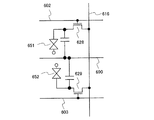
A display device obtained using each of the above manufacturing methods is also one embodiment of the present invention, and includes a gate electrode over a substrate, an insulating film over the gate electrode, and a gate electrode over the insulating film. A first semiconductor film containing an overlapping p-type impurity element or n-type impurity element, a buffer layer on the first semiconductor film, a second semiconductor film containing an n-type impurity element on the buffer layer, A display device includes a source electrode or a drain electrode over a second semiconductor film.
また、表示装置としては、発光装置や液晶表示装置を含む。発光装置は発光素子を含み
、液晶表示装置は液晶素子を含む。発光素子は、電流または電圧によって輝度が制御され
る素子をその範疇に含んでおり、具体的には無機EL(Electro Lumines
cence)、有機EL等が含まれる。
The display device includes a light emitting device and a liquid crystal display device. The light emitting device includes a light emitting element, and the liquid crystal display device includes a liquid crystal element. The light-emitting element includes, in its category, an element whose luminance is controlled by current or voltage, and specifically, an inorganic EL (Electro Lumines).
ence), organic EL, and the like.
また、表示装置は、表示素子が封止された状態にあるパネルと、該パネルにコントロー
ラを含むIC等を実装した状態にあるモジュールとを含む。さらに本発明は、該表示装置
を作製する過程における、表示素子が完成する前の一形態に相当する素子基板に関し、該
素子基板は、電流を表示素子に供給するための手段を複数の各画素に備える。素子基板は
、具体的には、表示素子の画素電極のみが形成された状態であっても良いし、画素電極と
なる導電膜を成膜した後であって、エッチングして画素電極を形成する前の状態であって
も良いし、あらゆる形態があてはまる。
The display device includes a panel in which the display element is sealed, and a module in which an IC including a controller is mounted on the panel. Furthermore, the present invention relates to an element substrate corresponding to one mode before the display element is completed in the process of manufacturing the display device, and the element substrate includes a unit for supplying current to the display element. Prepare for. Specifically, the element substrate may be in a state where only the pixel electrode of the display element is formed, or after the conductive film to be the pixel electrode is formed, the pixel electrode is formed by etching. The previous state may be used, and all forms are applicable.
なお、本明細書中における表示装置とは、画像表示デバイス、発光デバイス、もしくは光
源(照明装置含む)を指す。また、コネクター、例えばFPC(Flexible pr
inted circuit)もしくはTAB(Tape Automated Bon
ding)テープもしくはTCP(Tape Carrier Package)が取り
付けられたモジュール、TABテープやTCPの先にプリント配線板が設けられたモジュ
ール、または表示素子にCOG(Chip On Glass)方式によりIC(集積回
路)が直接実装されたモジュールも全て表示装置に含むものとする。
Note that a display device in this specification means an image display device, a light-emitting device, or a light source (including a lighting device). Also, a connector such as an FPC (Flexible pr
integrated circuit) or TAB (Tape Automated Bon)
ding) tape or TCP (Tape Carrier Package) attached module, TAB tape or TCP is provided with a printed wiring board, or a display element is an IC (integrated circuit) by COG (Chip On Glass) method. All directly mounted modules are included in the display device.
p型不純物元素またはn型不純物元素を含む微結晶半導体膜をチャネル形成領域として用
い、微結晶半導体膜に意図的に含ませたp型不純物元素またはn型不純物元素により、し
きい値電圧が所望の値に制御された薄膜トランジスタを実現することができる。
A microcrystalline semiconductor film containing a p-type impurity element or an n-type impurity element is used as a channel formation region, and a threshold voltage is desired by the p-type impurity element or the n-type impurity element intentionally included in the microcrystalline semiconductor film. A thin film transistor controlled to a value of can be realized.
本発明の実施形態について、以下に説明する。但し、本発明は多くの異なる態様で実施
することが可能であり、本発明の趣旨及びその範囲から逸脱することなくその形態及び詳
細を様々に変更し得ることは当業者であれば容易に理解される。従って、本実施の形態の
記載内容に限定して解釈されるものではない。
Embodiments of the present invention will be described below. However, the present invention can be implemented in many different modes, and those skilled in the art can easily understand that the modes and details can be variously changed without departing from the spirit and scope of the present invention. Is done. Therefore, the present invention is not construed as being limited to the description of this embodiment mode.
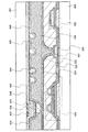
(実施の形態1)
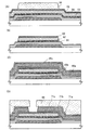
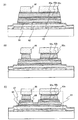
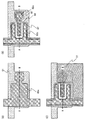
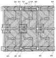
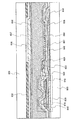
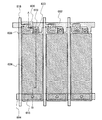
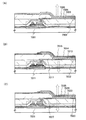
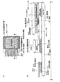
本実施の形態では、液晶表示装置に用いられる薄膜トランジスタの作製工程について、図
1乃至図4を用いて説明する。図1乃至図3は、薄膜トランジスタの作製工程を示す断面
図であり、図4は、一画素における薄膜トランジスタ及び画素電極の接続領域の上面図で
ある。
(Embodiment 1)
In this embodiment, a manufacturing process of a thin film transistor used for a liquid crystal display device will be described with reference to FIGS. 1 to 3 are cross-sectional views illustrating a manufacturing process of a thin film transistor, and FIG. 4 is a top view of a connection region between a thin film transistor and a pixel electrode in one pixel.
微結晶半導体膜を有する薄膜トランジスタはp型よりもn型の方が、移動度が高いので駆
動回路に用いるのにより適している。同一の基板上に形成する薄膜トランジスタを全て同
じ極性にそろえておくことが、工程数を抑えるためにも望ましい。ここでは、nチャネル
型の薄膜トランジスタを用いて説明する。
A thin film transistor including a microcrystalline semiconductor film is more suitable for use in a driver circuit because an n-type thin film transistor has higher mobility than a p-type. In order to reduce the number of steps, it is desirable that all thin film transistors formed over the same substrate have the same polarity. Here, description is made using an n-channel thin film transistor.
図1(A)に示すように、基板50上にゲート電極51を形成する。基板50は、バリ
ウムホウケイ酸ガラス、アルミノホウケイ酸ガラス、若しくはアルミノシリケートガラス
など、フュージョン法やフロート法で作製される無アルカリガラス基板、セラミック基板
の他、本作製工程の処理温度に耐えうる耐熱性を有するプラスチック基板等を用いること
もできる。また、ステンレス合金などの金属基板の表面に絶縁膜を設けた基板を適用して
も良い。基板50がマザーガラスの場合、基板の大きさは、第1世代(320mm×40
0mm)、第2世代(400mm×500mm)、第3世代(550mm×650mm)
、第4世代(680mm×880mm、または730mm×920mm)、第5世代(1
000mm×1200mmまたは1100mm×1250mm)、第6世代(1500m
m×1800mm)、第7世代(1900mm×2200mm)、第8世代(2160m
m×2460mm)、第9世代(2400mm×2800mm、2450mm×3050
mm)、第10世代(2950mm×3400mm)等を用いることができる。
As shown in FIG. 1A, a
0mm), 2nd generation (400mm x 500mm), 3rd generation (550mm x 650mm)
, 4th generation (680 mm x 880 mm, or 730 mm x 920 mm), 5th generation (1
000mm x 1200mm or 1100mm x 1250mm), 6th generation (1500m
m × 1800mm), 7th generation (1900mm × 2200mm), 8th generation (2160m)
m × 2460mm), 9th generation (2400mm × 2800mm, 2450mm × 3050)
mm), 10th generation (2950 mm × 3400 mm), or the like.
ゲート電極51は、チタン、モリブデン、クロム、タンタル、タングステン、アルミニウ
ムなどの金属材料またはその合金材料を用いて形成する。ゲート電極51は、スパッタリ
ング法や真空蒸着法で基板50上に導電膜を形成し、当該導電膜上にフォトリソグラフィ
技術またはインクジェット法によりマスクを形成し、当該マスクを用いて導電膜をエッチ
ングすることで、形成することができる。また、銀、金、銅などの導電性ナノペーストを
用いてインクジェット法により吐出し焼成して、ゲート電極51を形成することもできる
。なお、ゲート電極51の密着性向上と下地への拡散を防ぐバリアメタルとして、上記金
属材料の窒化物膜を、基板50及びゲート電極51の間に設けてもよい。ここでは、第1
のフォトマスクを用いて形成したレジストマスクを用いて基板50上に形成された導電膜
をエッチングしてゲート電極を形成する。
The
A gate electrode is formed by etching the conductive film formed over the
具体的なゲート電極構造の例としては、アルミニウム膜上にモリブデン膜を積層させ、ア
ルミニウム特有のヒロックやエレクトロマイグレーションを防ぐ構造にしてもよい。また
、アルミニウム膜をモリブデン膜で挟んだ3層構造としてもよい。また、他のゲート電極
構造の例として、銅膜上にモリブデン膜の積層、銅膜上に窒化チタン膜の積層、銅膜上に
窒化タンタル膜の積層が挙げられる。
As a specific example of the gate electrode structure, a molybdenum film may be stacked on an aluminum film to prevent a hillock or electromigration peculiar to aluminum. Alternatively, a three-layer structure in which an aluminum film is sandwiched between molybdenum films may be used. As another example of the gate electrode structure, a molybdenum film is laminated on a copper film, a titanium nitride film is laminated on the copper film, and a tantalum nitride film is laminated on the copper film.
なお、ゲート電極51上には半導体膜や配線を形成するので、段切れ防止のため端部が
テーパー状になるように加工することが望ましい。また、図示しないがこの工程でゲート
電極に接続する配線も同時に形成することができる。
Note that since a semiconductor film or a wiring is formed over the
次に、ゲート電極51上に、ゲート絶縁膜52a、52b、52c、微結晶半導体膜2
3aを順に形成する。ここまでの工程を終えた断面図が図1(A)に相当する。なお、ゲ
ート絶縁膜52a、52b、52c、微結晶半導体膜23aを大気に触れさせることなく
連続的に成膜することが好ましい。連続的に成膜することで大気成分や大気中に浮遊する
汚染不純物元素に汚染されることなく各積層界面を形成することができるので、薄膜トラ
ンジスタ特性のばらつきを低減することができる。
Next, on the
3a is formed in order. A cross-sectional view after the steps up to here corresponds to FIG. Note that the
ゲート絶縁膜52a、52b、52cはそれぞれ、CVD法やスパッタリング法等を用い
て、酸化珪素膜、窒化珪素膜、酸化窒化珪素膜、または窒化酸化珪素膜で形成することが
できる。ゲート絶縁膜52に形成されるピンホール等による層間ショートを防ぐため、異
なる絶縁層を用いて多層とすることが好ましい。ここでは、ゲート絶縁膜52a、52b
、52cとして、窒化珪素膜、酸化窒化珪素膜、窒化珪素膜の順に積層して形成する形態
を示す。
Each of the
52c, a silicon nitride film, a silicon oxynitride film, and a silicon nitride film are stacked in this order.
ここでは、酸化窒化珪素膜とは、その組成として、窒素よりも酸素の含有量が多いもので
あって、ラザフォード後方散乱法(RBS:Rutherford Backscatt
ering Spectrometry)及び水素前方散乱法(HFS:Hydroge
n Forward Scattering)を用いて測定した場合に、濃度範囲として
酸素が50〜70原子%、窒素が0.5〜15原子%、Siが25〜35原子%、水素が
0.1〜10原子%の範囲で含まれるものをいう。また、窒化酸化珪素膜とは、その組成
として、酸素よりも窒素の含有量が多いものであって、RBS及びHFSを用いて測定し
た場合に、濃度範囲として酸素が5〜30原子%、窒素が20〜55原子%、Siが25
〜35原子%、水素が10〜30原子%の範囲で含まれるものをいう。
Here, the silicon oxynitride film has a composition that contains more oxygen than nitrogen and has a Rutherford backscattering method (RBS: Rutherford Backscatter).
ering Spectrometry (HFS) and Hydrogen Forward Scattering (HFS)
n Forward Scattering), the concentration ranges from 50 to 70 atomic% for oxygen, 0.5 to 15 atomic% for nitrogen, 25 to 35 atomic% for Si, and 0.1 to 10 atomic% for hydrogen. The thing included in the range of. In addition, the silicon nitride oxide film has a nitrogen content higher than that of oxygen as a composition. When measured using RBS and HFS, the concentration range of oxygen is 5 to 30 atomic%, nitrogen. 20-55 atomic%, Si 25
-35 atomic% and hydrogen are contained in the range of 10-30 atomic%.
ゲート絶縁膜52の1層目及び2層目の膜厚はともに50nmよりも厚くする。ゲート絶
縁膜の1層目は、基板からの不純物(例えばアルカリ金属など)の拡散を防ぐために、窒
化珪素膜または窒化酸化珪素膜が好ましい。また、ゲート絶縁膜52の1層目は、ゲート
電極の酸化防止の他、ゲート電極にアルミニウムを用いる場合にヒロック防止ができる。
また、微結晶半導体膜と接するゲート絶縁膜52の3層目は、0nmより厚く10nm以
下とする。ゲート絶縁膜52の3層目は、微結晶半導体膜との密着性を向上させるために
設けるものである。また、ゲート絶縁膜52の3層目を窒化珪素膜とすることで後に行わ
れる熱処理やレーザ照射による微結晶半導体膜の酸化防止を図ることができる。例えば、
酸素の含有量が多い絶縁膜と微結晶半導体膜とを接した状態で熱処理を行うと、微結晶半
導体膜が酸化する恐れがある。
The film thicknesses of the first layer and the second layer of the gate insulating film 52 are both greater than 50 nm. The first layer of the gate insulating film is preferably a silicon nitride film or a silicon nitride oxide film in order to prevent diffusion of impurities (for example, alkali metal) from the substrate. Further, the first layer of the gate insulating film 52 can prevent hillocks when aluminum is used for the gate electrode in addition to preventing the oxidation of the gate electrode.
The third layer of the gate insulating film 52 in contact with the microcrystalline semiconductor film is greater than 0 nm and less than or equal to 10 nm. The third layer of the gate insulating film 52 is provided to improve adhesion with the microcrystalline semiconductor film. Further, the third layer of the gate insulating film 52 is a silicon nitride film, so that the microcrystalline semiconductor film can be prevented from being oxidized by heat treatment performed later or laser irradiation. For example,
When heat treatment is performed in a state where the insulating film with a high oxygen content is in contact with the microcrystalline semiconductor film, the microcrystalline semiconductor film may be oxidized.
更には、周波数が1GHzのマイクロ波プラズマCVD装置を用いてゲート絶縁膜52を
形成することが好ましい。マイクロ波プラズマCVD装置で形成した酸化窒化珪素膜、窒
化酸化珪素膜は、耐圧が高く、薄膜トランジスタの信頼性を高めることができる。
Furthermore, it is preferable to form the gate insulating film 52 using a microwave plasma CVD apparatus having a frequency of 1 GHz. A silicon oxynitride film and a silicon nitride oxide film formed with a microwave plasma CVD apparatus have high withstand voltage and can improve the reliability of the thin film transistor.
また、微結晶半導体膜23aは、非晶質と結晶構造(単結晶、多結晶を含む)の中間的な
構造の半導体を含む膜である。この半導体は、自由エネルギー的に安定な第3の状態を有
する半導体であって、短距離秩序を持ち格子歪みを有する結晶質なものであり、粒径が0
.5〜20nmの柱状または針状結晶が基板表面に対して法線方向に成長している。また
、微結晶半導体と非単結晶半導体とが混在している。微結晶半導体の代表例である微結晶
シリコンは、そのラマンスペクトルが単結晶シリコンを示す520.5cm−1よりも低
波数側に、シフトしている。即ち、単結晶シリコンを示す520.5cm−1とアモルフ
ァスシリコンを示す480cm−1の間に微結晶シリコンのラマンスペクトルのピークが
ある。また、未結合手(ダングリングボンド)を終端するため水素またはハロゲンを少な
くとも1原子%またはそれ以上含ませている。さらに、ヘリウム、アルゴン、クリプトン
、ネオンなどの希ガス元素を含ませて格子歪みをさらに助長させることで、安定性が増し
良好な微結晶半導体膜が得られる。このような微結晶半導体膜に関する記述は、例えば、
米国特許4,409,134号で開示されている。
The
. Columnar or needle crystals of 5 to 20 nm are grown in the normal direction with respect to the substrate surface. In addition, a microcrystalline semiconductor and a non-single-crystal semiconductor are mixed. Microcrystalline silicon which is a typical example of a microcrystalline semiconductor has its Raman spectrum shifted to a lower wave number than 520.5 cm −1 indicating single crystal silicon. That is, the peak of the Raman spectrum of microcrystalline silicon is between 520.5 cm −1 representing single crystal silicon and 480 cm −1 representing amorphous silicon. In addition, at least 1 atomic% or more of hydrogen or halogen is contained to terminate dangling bonds (dangling bonds). Further, by adding a rare gas element such as helium, argon, krypton, or neon to further promote lattice distortion, stability can be improved and a good microcrystalline semiconductor film can be obtained. A description of such a microcrystalline semiconductor film is, for example,
U.S. Pat. No. 4,409,134.
この微結晶半導体膜23aは、周波数が数十MHz〜数百MHzの高周波プラズマCV
D装置、または周波数が1GHz以上のマイクロ波プラズマCVD装置により形成するこ
とができる。代表的には、SiH4、Si2H6などの水素化珪素を水素で希釈して形成
することができる。また、水素化珪素及び水素に加え、ヘリウム、アルゴン、クリプトン
、ネオンから選ばれた一種または複数種の希ガス元素で希釈して微結晶半導体膜を形成す
ることができる。これらのときの水素化珪素に対して水素の流量比を12倍以上1000
倍以下、好ましくは50倍以上200倍以下、更に好ましくは100倍とする。なお、水
素化珪素の代わりに、SiH2Cl2、SiHCl3、SiCl4、SiF4等を用いる
ことができる。
The
It can be formed by a D apparatus or a microwave plasma CVD apparatus having a frequency of 1 GHz or more. Typically, silicon hydride such as SiH 4 or Si 2 H 6 can be formed by diluting with hydrogen. In addition to silicon hydride and hydrogen, the microcrystalline semiconductor film can be formed by dilution with one or more kinds of rare gas elements selected from helium, argon, krypton, and neon. The flow rate ratio of hydrogen to silicon hydride at these times is 12 times or more and 1000
Double or less, preferably 50 times or more and 200 times or less, and more preferably 100 times. Note that SiH 2 Cl 2 , SiHCl 3 , SiCl 4 , SiF 4, or the like can be used instead of silicon hydride.
また、微結晶半導体膜23aの酸素濃度を、5×10¹⁹atoms/cm3以下、好
ましくは1×10¹⁹atoms/cm3以下、窒素及び炭素の濃度それぞれを3×10
18atoms/cm3以下とすることが好ましい。酸素、窒素、及び炭素が微結晶半導
体膜に混入する濃度を低減することで、微結晶半導体膜がn型化になることを防止するこ
とができる。
Further, the oxygen concentration of the
It is preferable to be 18 atoms / cm 3 or less. By reducing the concentration of oxygen, nitrogen, and carbon in the microcrystalline semiconductor film, the microcrystalline semiconductor film can be prevented from becoming n-type.
微結晶半導体膜23aの膜厚は、1nm以上20nm以下、好ましくは2nm以上10n
m未満とする。後で行うLP処理において、微結晶半導体膜23aの膜厚が4nm〜8n
mであればレーザビームの吸収率を高めることができるため、2nm以上10nm未満と
することが好ましい。微結晶半導体膜23aを上記膜厚範囲とすることで、後に形成され
る薄膜トランジスタは、完全空乏型となる。また、微結晶半導体膜23aは成膜速度が非
晶質半導体膜の成膜速度の1/10〜1/100と遅いため、膜厚を薄くすることでスル
ープットを向上させることができる。
The thickness of the
less than m. In LP treatment performed later, the thickness of the
If m, the absorption rate of the laser beam can be increased, and therefore, it is preferably 2 nm or more and less than 10 nm. By setting the
また、微結晶半導体膜23aを成膜する前に、ゲート絶縁膜52cの表面を水素プラズマ
処理してもよい。水素プラズマ処理することにより、ゲート絶縁膜及び微結晶半導体膜の
界面における格子歪を低減することが可能であり、ゲート絶縁膜及び微結晶半導体膜の界
面特性を向上させることができる。このため、後に形成される薄膜トランジスタの電気特
性を向上させることができる。
Alternatively, the surface of the
次いで、しきい値制御のために、一導電性を付与する不純物元素をイオン注入法により意
図的に添加する。成膜直後の微結晶半導体膜23aは、弱いn型の電気伝導性を示すため
、ここでは、ボロンを微量に添加して、しきい値制御を行うチャネルドーピングを行う。
こうして、図1(B)に示すように、ボロンを含む微結晶半導体膜23bが得られる。イ
オン注入することにより、成膜直後の微結晶半導体膜23aに比べて、ボロンを含む微結
晶半導体膜23bは結晶性が低下する。
Next, an impurity element imparting one conductivity is intentionally added by ion implantation for threshold control. Since the
Thus, as shown in FIG. 1B, a
次いで、成膜直後の微結晶半導体膜23aよりも結晶性を改善するため、微結晶半導体膜
の表面側からレーザビームを照射する。レーザビームのエネルギーは微結晶半導体膜が溶
融しないエネルギーで照射する。ゲート電極51が下方に存在するため、レーザビームに
よる熱が拡散することを考慮してエネルギー範囲を決定すればよい。従って、レーザビー
ムのエネルギーによっては、ゲート電極51と重ならない領域の微結晶半導体膜は溶融す
る一方、ゲート電極51と重なる領域は溶融しないこともある。ゲート電極51と重なる
領域とゲート電極と重ならない領域とでは形成される膜質が異なるため、本実施の形態で
は、薄膜トランジスタとして用いる半導体層は、ゲート電極と重なる領域のみ、好ましく
はゲート電極のテーパー部を除き、ゲート電極と重なる領域を用いる。膜質が同じ微結晶
半導体膜をチャネル形成領域とすることで、複数の薄膜トランジスタ間の特性バラツキを
低減することができる。
Next, in order to improve the crystallinity of the
レーザビームは微結晶半導体膜とゲート絶縁膜52cの界面にまで作用させることができ
る。それにより、微結晶半導体膜の表面側における結晶を種として、該表面からゲート絶
縁膜の界面において固相結晶成長し、結晶性が改善された微結晶半導体膜、所謂LPSA
S膜53を形成することができる(図1(C)参照)。LP処理による固相結晶成長は、
結晶粒径を拡大させるものではなく、むしろ膜の厚さ方向における結晶性を改善するもの
である。即ち、LP処理により、微結晶半導体膜のゲート絶縁膜近傍の結晶性が改善され
、ボトムゲート構造を有する薄膜トランジスタの電気的特性を向上させる作用を奏する。
The laser beam can be applied to the interface between the microcrystalline semiconductor film and the
An
It does not increase the crystal grain size, but rather improves the crystallinity in the thickness direction of the film. In other words, the LP treatment improves the crystallinity of the microcrystalline semiconductor film in the vicinity of the gate insulating film and improves the electrical characteristics of the thin film transistor having the bottom gate structure.
さらに、ここでのLP処理は、微結晶半導体膜に添加されたボロンを活性化させることも
できる。微結晶半導体膜に含まれるボロンにより、しきい値電圧が所望の値に制御された
薄膜トランジスタを得ることができる。例えば、微結晶半導体膜に含まれるボロンにより
、しきい値電圧を0Vまたはマイナス側のしきい値電圧に制御できれば、薄膜トランジス
タのゲートに印加するゲート電圧を0Vとした場合に、薄膜トランジスタがオフ状態とな
るノーマリーオフのスイッチング素子とすることができる。
Further, the LP treatment here can also activate boron added to the microcrystalline semiconductor film. A thin film transistor whose threshold voltage is controlled to a desired value can be obtained using boron contained in the microcrystalline semiconductor film. For example, if the threshold voltage can be controlled to 0 V or a negative threshold voltage by boron contained in the microcrystalline semiconductor film, the thin film transistor is turned off when the gate voltage applied to the gate of the thin film transistor is 0 V. It can be set as the normally-off switching element.
レーザビームとして、エキシマレーザを用いる場合はパルス発振周波数1Hz以上10M
Hz未満、好ましくは100Hz〜10kHzとし、レーザエネルギーを0.2〜0.3
5J/cm2(代表的には0.2〜0.3J/cm2)とする。また、YAGレーザを用
いる場合にはその第3高調波を用いパルス発振周波数1Hz以上10MHz未満とし、レ
ーザエネルギーを0.2〜0.35J/cm2(代表的には0.2〜0.3J/cm2)
とすると良い。
When an excimer laser is used as the laser beam, a pulse oscillation frequency of 1 Hz to 10 M
Less than Hz, preferably 100 Hz to 10 kHz, and the laser energy is 0.2 to 0.3.
5 J / cm 2 (typically 0.2 to 0.3 J / cm 2 ). When a YAG laser is used, the third harmonic is used and the pulse oscillation frequency is set to 1 Hz or more and less than 10 MHz, and the laser energy is set to 0.2 to 0.35 J / cm 2 (typically 0.2 to 0.3 J). / Cm 2 )
And good.
レーザビームを発振するレーザ発振器としては、パルス発振または連続発振することが可
能なレーザ発振器を用いることができる。また、レーザ波長は、半導体膜に効率よくレー
ザビームが吸収されるように可視〜紫外領域(800nm以下)、好ましくは紫外領域(
400nm以下)とする。波長が300nm〜400nmの紫外領域のレーザビームを照
射することで、微結晶半導体膜に効率良く吸収される。レーザ発振器としては、KrF、
ArF、XeCl、XeF等のエキシマレーザ発振器、N2、He、He−Cd、Ar、
He−Ne、HF、CO2等の気体レーザ発振器、YAG、GdVO4、YVO4、YL
F、YAlO3、ScO3、Lu2O3、Y2O3などの結晶にCr、Nd、Er、Ho
、Ce、Co、Ti、Yb、又はTmをドープした結晶を使った固体レーザ発振器、KG
Wレーザ、KYWレーザ、アレキサンドライトレーザ、Ti:サファイアレーザ等固体レ
ーザ、ヘリウムカドミウムレーザ等の金属蒸気レーザ発振器等を用いることができる。な
お、固体レーザ発振器においては、基本波の第2高調波〜第5高調波を適用するのが好ま
しい。
As a laser oscillator that oscillates a laser beam, a laser oscillator capable of pulse oscillation or continuous oscillation can be used. The laser wavelength is in the visible to ultraviolet region (800 nm or less), preferably in the ultraviolet region so that the semiconductor film can be efficiently absorbed by the semiconductor film.
400 nm or less). By irradiation with a laser beam in the ultraviolet region with a wavelength of 300 nm to 400 nm, the microcrystalline semiconductor film is efficiently absorbed. As a laser oscillator, KrF,
Excimer laser oscillators such as ArF, XeCl, XeF, N 2 , He, He—Cd, Ar,
He-Ne, HF, gas laser oscillator such as CO 2, YAG, GdVO 4, YVO 4, YL
Crystals of F, YAlO 3 , ScO 3 , Lu 2 O 3 , Y 2 O 3, etc. are added to Cr, Nd, Er, Ho
, Ce, Co, Ti, Yb, or solid state laser oscillator using crystal doped with Tm, KG
A solid-state laser such as a W laser, a KYW laser, an alexandrite laser, a Ti: sapphire laser, a metal vapor laser oscillator such as a helium cadmium laser, or the like can be used. In the solid-state laser oscillator, it is preferable to apply the second to fifth harmonics of the fundamental wave.
代表的には、レーザビームとして波長400nm以下、代表的には308nmのエキシ
マレーザビームや、YAGレーザの第3高調波(355nm)を用いる。
Typically, an excimer laser beam having a wavelength of 400 nm or less, typically 308 nm, or the third harmonic (355 nm) of a YAG laser is used as the laser beam.
LP処理は矩形長尺状に集光し、線状レーザビームとすることで、例えば730mm×9
20mmのガラス基板上の微結晶半導体膜23bを1回のレーザビームスキャンで処理す
ることができる。この場合、線状レーザビームを重ね合わせる割合(オーバーラップ率)
を0〜95%(好ましくは0〜67%)として行う。これにより、基板1枚当たりの処理
時間が短縮され、生産性を向上させることができる。レーザビームの形状は線状に限定さ
れるものでなく面状としても同様に処理することができる。また、本LP処理は前記ガラ
ス基板のサイズに限定されず、さまざまなものに適用することができる。
The LP process is focused into a rectangular long shape to form a linear laser beam, for example, 730 mm × 9
The
0 to 95% (preferably 0 to 67%). Thereby, the processing time per substrate can be shortened and productivity can be improved. The shape of the laser beam is not limited to a linear shape, and it can be similarly processed even if it is a planar shape. Further, the present LP treatment is not limited to the size of the glass substrate, and can be applied to various things.
また、レーザビームとして、連続発振のレーザビームを用いる場合、ポリゴンミラーやガ
ルバノミラーを発振器及び基板の間に設け、レーザビームを高速で走査することで、LP
処理のスループットを向上させることが可能であり、例えば730mm×920mmのガ
ラス基板や更にそれより大きいガラス基板上に形成される微結晶半導体膜をLP処理する
ことが可能である。
When a continuous oscillation laser beam is used as the laser beam, a polygon mirror or a galvano mirror is provided between the oscillator and the substrate, and the laser beam is scanned at a high speed, so that the LP
The throughput of the treatment can be improved. For example, a microcrystalline semiconductor film formed over a 730 mm × 920 mm glass substrate or a larger glass substrate can be subjected to LP treatment.
なお、アルゴン雰囲気、水素雰囲気、アルゴン及び水素雰囲気、窒素雰囲気等でレーザビ
ームを微結晶半導体膜23bに照射してもよい。このように、不活性な雰囲気でレーザビ
ームを微結晶半導体膜に照射することで、LPSAS膜53の表面に酸化膜が形成されに
くい。
Note that the
また、微結晶半導体膜23bにレーザビームを照射する前に、微結晶半導体膜23bの表
面を洗浄することで、チャネルドーピングの際などで微結晶半導体膜23b表面に付着す
る不純物がレーザビームの照射により、微結晶半導体膜中に混入するのを防ぐことができ
る。
In addition, by cleaning the surface of the
また、微結晶半導体膜にレーザビームを照射すると共に、微結晶半導体膜を加熱してもよ
い。代表的には、基板50を300℃〜400℃で加熱しながら、レーザビームを照射す
ることで、微結晶半導体膜23bの結晶性を高めることが可能である。または、微結晶半
導体膜23bにレーザビームを照射すると共に、強光を照射して、瞬間的に微結晶半導体
膜23bの温度を上昇させてもよい。強光の代表例としては、赤外光、特に1μm〜2μ
mにピークを有する赤外光(好ましくはハロゲン光(1.3μm))を用いることができ
る。
In addition, the microcrystalline semiconductor film may be irradiated with a laser beam and the microcrystalline semiconductor film may be heated. Typically, the crystallinity of the
Infrared light having a peak at m (preferably halogen light (1.3 μm)) can be used.
次いで、図1(D)に示すように、LPSAS膜53上にバッファ層54及び一導電型を
付与する不純物が添加された半導体膜55を形成する。レーザビームの照射によりLPS
AS膜53表面に酸化膜が形成された場合には、バッファ層54を形成する前に除去する
ことが好ましい。
Next, as illustrated in FIG. 1D, a
When an oxide film is formed on the surface of the
バッファ層54は、水素、窒素、若しくはハロゲンを含む非晶質半導体膜を用いて形成す
る。水素化珪素の流量の1倍以上10倍以下、更に好ましくは1倍以上5倍以下の流量の
水素を用いて、水素を含む非晶質半導体膜を形成することができる。また、上記水素化珪
素と窒素またはアンモニアとを用いることで、窒素を含む非晶質半導体膜を形成すること
ができる。また、上記水素化珪素と、フッ素、塩素、臭素、またはヨウ素を含む気体(F
2、Cl2、Br2、I2、HF、HCl、HBr、HI等)を用いることで、フッ素、
塩素、臭素、またはヨウ素を含む非晶質半導体膜を形成することができる。なお、水素化
珪素の代わりに、SiH2Cl2、SiHCl3、SiCl4、SiF4等を用いること
ができる。
The
2 , Cl 2 , Br 2 , I 2 , HF, HCl, HBr, HI, etc.)
An amorphous semiconductor film containing chlorine, bromine, or iodine can be formed. Note that SiH 2 Cl 2 , SiHCl 3 , SiCl 4 , SiF 4, or the like can be used instead of silicon hydride.
また、バッファ層54は、ターゲットに非晶質半導体を用いて水素、または希ガスでスパ
ッタリングして非晶質半導体膜を形成することができる。このとき、アンモニア、窒素、
またはN2Oを雰囲気中に含ませることにより、窒素を含む非晶質半導体膜を形成するこ
とができる。また、雰囲気中にフッ素、塩素、臭素、またはヨウ素を含む気体(F2、C
l2、Br2、I2、HF、HCl、HBr、HI等)を含ませることにより、フッ素、
塩素、臭素、またはヨウ素を含む非晶質半導体膜を形成することができる。
The
Alternatively, by containing N 2 O in the atmosphere, an amorphous semiconductor film containing nitrogen can be formed. In addition, a gas containing fluorine, chlorine, bromine, or iodine in the atmosphere (F 2 , C
l 2 , Br 2 , I 2 , HF, HCl, HBr, HI, etc.)
An amorphous semiconductor film containing chlorine, bromine, or iodine can be formed.
また、バッファ層54として、LPSAS膜53の表面にプラズマCVD法またはスパッ
タリング法により非晶質半導体膜を形成した後、非晶質半導体膜の表面を水素プラズマ、
窒素プラズマ、またはハロゲンプラズマで処理して、非晶質半導体膜の表面を水素化、窒
素化、またはハロゲン化してもよい。または、非晶質半導体膜の表面を、ヘリウムプラズ
マ、ネオンプラズマ、アルゴンプラズマ、クリプトンプラズマ等で処理してもよい。
As the
The surface of the amorphous semiconductor film may be hydrogenated, nitrogenated, or halogenated by treatment with nitrogen plasma or halogen plasma. Alternatively, the surface of the amorphous semiconductor film may be treated with helium plasma, neon plasma, argon plasma, krypton plasma, or the like.
バッファ層54は、結晶粒を含まない非晶質半導体膜で形成することが好ましい。このた
め、周波数が数十MHz〜数百MHzの高周波プラズマCVD法、またはマイクロ波プラ
ズマCVD法で形成する場合は、結晶粒を含まない非晶質半導体膜となるように、成膜条
件を制御することが好ましい。
The
バッファ層54は、後のソース領域及びドレイン領域の形成プロセスにおいて、一部エッ
チングする。そのときに、LPSAS膜53が露呈しないようにバッファ層54の一部が
残存する厚さで形成することが好ましい。代表的には、100nm以上400nm以下、
好ましくは200nm以上300nm以下の厚さで形成することが好ましい。薄膜トラン
ジスタの印加電圧の高い(例えば15V程度)表示装置、代表的には液晶表示装置におい
て、バッファ層54の膜厚を上記範囲に示すように厚く形成すると、耐圧が高くなり、薄
膜トランジスタに高い電圧が印加されても、薄膜トランジスタが劣化することを回避する
ことができる。
The
Preferably, it is formed with a thickness of 200 nm to 300 nm. In a display device with a high applied voltage of the thin film transistor (for example, about 15 V), typically a liquid crystal display device, when the
なお、バッファ層54には、リンやボロン等の一導電型を付与する不純物が添加されてい
ない。LPSAS膜53にはしきい値を制御するために微量のボロンを含ませているため
、一導電型を付与する不純物が添加された半導体膜55から不純物がLPSAS膜へ拡散
しないように、バッファ層54がバリア層として機能している。バッファ層を設けない場
合、LPSAS膜と一導電型を付与する不純物が添加された半導体膜55とが接してしま
うと、後のエッチング工程や加熱処理により不純物が移動し、しきい値制御が困難になる
恐れがある。
Note that an impurity imparting one conductivity type, such as phosphorus or boron, is not added to the
さらにバッファ層54をLPSAS膜53の表面上に形成することで、LPSAS膜53
に含まれる結晶粒の表面の自然酸化を防止することが可能である。特に、非晶質半導体と
微結晶粒が接する領域では、局部応力により亀裂が入りやすい。この亀裂が酸素に触れる
と結晶粒は酸化され、酸化珪素が形成される。
Further, by forming the
It is possible to prevent natural oxidation of the surface of the crystal grains contained in. In particular, in a region where an amorphous semiconductor is in contact with microcrystalline grains, cracks are likely to occur due to local stress. When this crack comes into contact with oxygen, the crystal grains are oxidized and silicon oxide is formed.
非晶質半導体膜であるバッファ層54のエネルギーギャップがLPSAS膜53に比べて
大きく(非晶質半導体膜のエネルギーギャップは1.6〜1.8eV、LPSAS膜53
のエネルギーギャップは1.1〜1.5eV)、また抵抗が高く、移動度が低く、LPS
AS膜53の1/5〜1/10である。このため、後に形成される薄膜トランジスタにお
いて、ソース領域及びドレイン領域と、LPSAS膜53との間に形成されるバッファ層
は高抵抗領域として機能し、LPSAS膜53がチャネル形成領域として機能する。この
ため、薄膜トランジスタのオフ電流を低減することができる。当該薄膜トランジスタを表
示装置のスイッチング素子として用いた場合、表示装置のコントラストを向上させること
ができる。
The energy gap of the
Has an energy gap of 1.1 to 1.5 eV), high resistance, low mobility, and LPS
It is 1/5 to 1/10 of the
なお、LPSAS膜53上に、プラズマCVD法によりバッファ層54を300℃〜40
0℃の温度にて成膜することが好ましい。この成膜処理により水素がLPSAS膜53に
供給され、LPSAS膜53を水素化したのと同等の効果が得られる。すなわち、LPS
AS膜53上にバッファ層54を堆積することにより、LPSAS膜53に水素を拡散さ
せて、ダングリングボンドの終端をすることができる。
A
It is preferable to form a film at a temperature of 0 ° C. By this film forming process, hydrogen is supplied to the
By depositing the
また、一導電型を付与する不純物が添加された半導体膜55は、nチャネル型の薄膜トラ
ンジスタを形成する場合には、代表的な不純物元素としてリンを添加すれば良く、水素化
珪素にPH3などの不純物気体を加えれば良い。また、pチャネル型の薄膜トランジスタ
を形成する場合には、代表的な不純物元素としてボロンを添加すれば良く、水素化珪素に
B2H6などの不純物気体を加えれば良い。一導電型を付与する不純物が添加された半導
体膜55は、微結晶半導体、または非晶質半導体で形成することができる。一導電型を付
与する不純物が添加された半導体膜55は2nm以上50nm以下の厚さで形成する。一
導電型を付与する不純物が添加された半導体膜の膜厚を、薄くすることでスループットを
向上させることができる。
In the case of forming an n-channel thin film transistor, the
次いで、図2(A)に示すように、一導電型を付与する不純物が添加された半導体膜55
上にレジストマスク56を形成する。レジストマスク56は、フォトリソグラフィ技術ま
たはインクジェット法により形成する。ここでは、第2のフォトマスクを用いて、一導電
型を付与する不純物が添加された半導体膜55上に塗布されたレジストを露光現像して、
レジストマスク56を形成する。
Next, as shown in FIG. 2A, a
A resist
A resist
次いで、レジストマスク56を用いてLPSAS膜53、バッファ層54、及び導電型を
付与する不純物が添加された半導体膜55をエッチングし分離して、図2(B)に示すよ
うに、LPSAS膜61、バッファ層62、及び一導電型を付与する不純物が添加された
半導体膜63を形成する。この後、レジストマスク56を除去する。
Next, the
LPSAS膜61、バッファ層62の端部側面が傾斜していることにより、バッファ層6
2上に形成されるソース領域及びドレイン領域とLPSAS膜61との間にリーク電流が
生じることを防止することが可能である。また、ソース電極及びドレイン電極と、LPS
AS膜61との間にリーク電流が生じるのを防止することが可能である。LPSAS膜6
1及びバッファ層62の端部側面の傾斜角度は、90°〜30°、好ましくは80°〜4
5°である。このような角度とすることで、段差形状によるソース電極またはドレイン電
極の段切れを防ぐことができる。
Since the side surfaces of the end portions of the
It is possible to prevent a leak current from being generated between the source region and the drain region formed on 2 and the
It is possible to prevent a leak current from occurring between the
1 and the angle of inclination of the side surface of the
5 °. With such an angle, disconnection of the source electrode or drain electrode due to the step shape can be prevented.
次に、図2(C)に示すように、一導電型を付与する不純物が添加された半導体膜63及
びゲート絶縁膜52cを覆うように導電膜65a〜65cを形成する。導電膜65a〜6
5cは、アルミニウム、銅、又はシリコン、チタン、ネオジム、スカンジウム、モリブデ
ンなどの耐熱性向上元素若しくはヒロック防止元素が添加されたアルミニウム合金の単層
または積層で形成することが好ましい。また、一導電型を付与する不純物が添加された半
導体膜と接する側の膜を、チタン、タンタル、モリブデン、タングステン、またはこれら
の元素の窒化物で形成し、その上にアルミニウムまたはアルミニウム合金を形成した積層
構造としても良い。更には、アルミニウムまたはアルミニウム合金の上面及び下面を、チ
タン、タンタル、モリブデン、タングステン、またはこれらの元素の窒化物で挟んだ積層
構造としてもよい。ここでは、導電膜としては、導電膜65a〜65c3層が積層した構
造の導電膜を示し、導電膜65a、65cにモリブデン膜、導電膜65bにアルミニウム
膜を用いた積層導電膜や、導電膜65a、65cにチタン膜、導電膜65bにアルミニウ
ム膜を用いた積層導電膜を示す。導電膜65a〜65cは、スパッタリング法や真空蒸着
法で形成する。
Next, as illustrated in FIG. 2C,
5c is preferably formed of a single layer or a stack of aluminum, copper, or an aluminum alloy to which a heat resistance improving element such as silicon, titanium, neodymium, scandium, or molybdenum or a hillock prevention element is added. In addition, a film in contact with a semiconductor film to which an impurity imparting one conductivity type is added is formed using titanium, tantalum, molybdenum, tungsten, or a nitride of these elements, and aluminum or an aluminum alloy is formed thereover. It is good also as a laminated structure. Furthermore, a laminated structure in which the upper and lower surfaces of aluminum or an aluminum alloy are sandwiched between titanium, tantalum, molybdenum, tungsten, or nitrides of these elements may be employed. Here, a conductive film having a structure in which
次に、図2(D)に示すように、導電膜65a〜65c上に第3のフォトマスクを用いて
レジストマスク66を形成し、導電膜65a〜65cの一部をエッチングして一対のソー
ス電極及びドレイン電極71a〜71cを形成する。導電膜65a〜65cをウエットエ
ッチングすると、導電膜65a〜65cが選択的にエッチングされる。この結果、導電膜
を等方的にエッチングするため、レジストマスク66より面積の小さいソース電極及びド
レイン電極71a〜71cを形成することができる。
Next, as illustrated in FIG. 2D, a resist
次に、図3(A)に示すように、レジストマスク66を用いて一導電型を付与する不純物
が添加された半導体膜63をエッチングして、一対のソース領域及びドレイン領域72を
形成する。さらに、当該エッチング工程において、バッファ層62の一部もエッチングす
る。一部エッチングされた、窪み(溝)が形成されたバッファ層をバッファ層73と示す
。ソース領域及びドレイン領域の形成工程と、バッファ層の窪み(溝)とを同一工程で形
成することができる。バッファ層の窪み(溝)の深さをバッファ層の一番膜厚の厚い領域
の1/2〜1/3とすることで、ソース領域及びドレイン領域の距離を離すことが可能で
あるため、ソース領域及びドレイン領域の間でのリーク電流を低減することができる。こ
の後、レジストマスク66を除去する。
Next, as illustrated in FIG. 3A, the
特にドライエッチングなどで用いるプラズマに曝されるとレジストマスクは変質し、レジ
スト除去工程で完全には除去されず、残渣が残ることを防ぐためにバッファ層を50nm
程度エッチングする。レジストマスク66は、導電膜65a〜65cの一部のエッチング
処理と、ソース領域及びドレイン領域72の形成時のエッチング処理の2回に用いられて
おり、どちらもドライエッチングを用いる場合には、残渣が残りやすいため、残渣を完全
に除去する際にエッチングされてもよいバッファ層の膜厚を厚く形成することは有効であ
る。また、バッファ層73は、ドライエッチングの際にプラズマダメージがLPSAS膜
61に与えられることを防止することもできる。
In particular, when exposed to plasma used for dry etching, the resist mask changes in quality and is not completely removed in the resist removal process, so that a buffer layer is formed with a thickness of 50 nm to prevent residues.
Etch to a certain extent. The resist
次に、図3(B)に示すように、ソース電極及びドレイン電極71a〜71c、ソース領
域及びドレイン領域72、バッファ層73、LPSAS膜61、及びゲート絶縁膜52c
を覆う絶縁膜76を形成する。絶縁膜76は、ゲート絶縁膜52a、52b、52cと同
じ成膜方法を用いて形成することができる。なお、絶縁膜76は、大気中に浮遊する有機
物や金属物、水蒸気などの汚染不純物の侵入を防ぐためのものであり、緻密な膜が好まし
い。また、絶縁膜76に窒化珪素膜を用いることで、バッファ層73中の酸素濃度を5×
1019atoms/cm3以下、好ましくは1×1019atoms/cm3以下とす
ることができる。
Next, as shown in FIG. 3B, the source and
An insulating
It can be 10 19 atoms / cm 3 or less, preferably 1 × 10 19 atoms / cm 3 or less.
図3(B)に示すように、ソース電極及びドレイン電極71a〜71cの端部と、ソース
領域及びドレイン領域72の端部は一致せずずれた形状となることで、ソース電極及びド
レイン電極71a〜71cの端部の距離が離れるため、ソース電極及びドレイン電極間の
リーク電流やショートを防止することができる。また、ソース電極及びドレイン電極71
a〜71cの端部と、ソース領域及びドレイン領域72の端部は一致せずずれた形状であ
るため、ソース電極及びドレイン電極71a〜71c及びソース領域及びドレイン領域7
2の端部に電界が集中せず、ゲート電極51と、ソース電極及びドレイン電極71a〜7
1cとの間でのリーク電流を防止することができる。このため、信頼性が高く、且つ耐圧
の高い薄膜トランジスタを作製することができる。さらに、チャネルドープが行われ、し
きい値制御された薄膜トランジスタを作製することができる。
As shown in FIG. 3B, the end portions of the source and
Since the end portions of a to 71c and the end portions of the source region and the
2, the electric field is not concentrated on the end portion of the
Leakage current with 1c can be prevented. Therefore, a thin film transistor with high reliability and high withstand voltage can be manufactured. Further, a thin film transistor in which channel doping is performed and the threshold value is controlled can be manufactured.
以上の工程により、チャネルエッチ型の薄膜トランジスタ74を形成することができる
。
Through the above process, a channel-etched
本実施の形態で示す薄膜トランジスタは、ゲート電極上にゲート絶縁膜、LPSAS膜、
バッファ層、ソース領域及びドレイン領域、ソース電極及びドレイン電極が積層され、チ
ャネル形成領域として機能するLPSAS膜の表面をバッファ層が覆う。また、バッファ
層の一部には窪み(溝)が形成されており、当該窪み以外の領域がソース領域及びドレイ
ン領域で覆われる。即ち、バッファ層に形成される窪みにより、ソース領域及びドレイン
領域の距離が離れているため、ソース領域及びドレイン領域の間でのリーク電流を低減す
ることができる。また、バッファ層の一部をエッチングすることにより窪みを形成するた
め、ソース領域及びドレイン領域の形成工程において発生するエッチング残渣を除去する
ことができるため、残渣を介してソース領域及びドレイン領域にリーク電流(寄生チャネ
ル)が発生することを回避することができる。
In the thin film transistor described in this embodiment, a gate insulating film, an LPSAS film,
The buffer layer, the source and drain regions, the source electrode and the drain electrode are stacked, and the buffer layer covers the surface of the LPSAS film functioning as a channel formation region. Further, a depression (groove) is formed in a part of the buffer layer, and a region other than the depression is covered with the source region and the drain region. In other words, since the distance between the source region and the drain region is increased due to the depression formed in the buffer layer, leakage current between the source region and the drain region can be reduced. Further, since the depression is formed by etching a part of the buffer layer, the etching residue generated in the step of forming the source region and the drain region can be removed, so that the leakage to the source region and the drain region through the residue. Generation of a current (parasitic channel) can be avoided.
また、チャネル形成領域として機能するLPSAS膜とソース領域及びドレイン領域との
間に、バッファ層が形成されている。また、LPSAS膜の表面がバッファ層で覆われて
いる。高抵抗のバッファ層は、LPSAS膜と、ソース領域及びドレイン領域との間にま
で延在しているため、薄膜トランジスタにリーク電流が発生することを低減することがで
きると共に、高い電圧の印加による劣化を低減することができる。また、バッファ層と、
LPSAS膜と、ソース領域及びドレイン領域は、全てゲート電極と重なる領域上に形成
される。従って、ゲート電極の端部形状に影響されない構造と言える。ゲート電極を積層
構造とした場合、下層としてアルミニウムを用いると、ゲート電極側面にアルミニウムが
露出し、ヒロックが発生する恐れがあるが、さらにソース領域及びドレイン領域をゲート
電極端部とも重ならない構成とすることで、ゲート電極側面と重なる領域でショートが発
生することを防ぐことができる。また、LPSAS膜の表面に水素で表面が終端された非
晶質半導体膜がバッファ層として形成されているため、LPSAS膜の酸化を防止するこ
とが可能であると共に、ソース領域及びドレイン領域の形成工程に発生するエッチング残
渣がLPSAS膜に混入することを防ぐことができる。従って、電気特性が優れ、且つ耐
圧に優れた薄膜トランジスタを形成することができる。
In addition, a buffer layer is formed between the LPSAS film functioning as a channel formation region and the source and drain regions. The surface of the LPSAS film is covered with a buffer layer. The high-resistance buffer layer extends between the LPSAS film and the source region and the drain region, so that generation of a leakage current in the thin film transistor can be reduced, and deterioration due to application of a high voltage. Can be reduced. And a buffer layer,
The LPSAS film, the source region, and the drain region are all formed on a region overlapping with the gate electrode. Therefore, it can be said that the structure is not affected by the end shape of the gate electrode. When the gate electrode has a laminated structure, if aluminum is used as the lower layer, aluminum may be exposed on the side surface of the gate electrode and hillocks may be generated, but the source region and the drain region do not overlap the gate electrode end. By doing so, it is possible to prevent a short circuit from occurring in a region overlapping with the side surface of the gate electrode. Further, since an amorphous semiconductor film whose surface is terminated with hydrogen is formed as a buffer layer on the surface of the LPSAS film, it is possible to prevent the LPSAS film from being oxidized and to form a source region and a drain region. Etching residues generated in the process can be prevented from entering the LPSAS film. Therefore, a thin film transistor having excellent electric characteristics and excellent withstand voltage can be formed.
また、薄膜トランジスタのチャネル長を短くすることができ、薄膜トランジスタの平面積
を縮小することができる。
In addition, the channel length of the thin film transistor can be shortened, and the plane area of the thin film transistor can be reduced.
次に、絶縁膜76に第4のフォトマスクを用いて形成したレジストマスクを用いて絶縁膜
76の一部をエッチングしてコンタクトホールを形成し、当該コンタクトホールにおいて
ソース電極またはドレイン電極71cに接する画素電極77を形成する。なお、図3(C
)は、図4の鎖線A−Bの断面図に相当する。
Next, a part of the insulating
) Corresponds to a cross-sectional view taken along chain line AB in FIG.
図4に示すように、ソース領域及びドレイン領域72の端部は、ソース電極及びドレイン
電極71cの端部の外側に位置することが分かる。また、バッファ層73の端部はソース
電極及びドレイン電極71c及びソース領域及びドレイン領域72の端部の外側に位置す
る。また、ソース電極及びドレイン電極の一方はソース電極及びドレイン電極の他方を囲
む形状(具体的には、U字型、C字型)である。このため、キャリアが移動する領域の面
積を増加させることが可能であるため、電流量を増やすことが可能であり、薄膜トランジ
スタの面積を縮小することができる。また、ゲート電極上において、LPSAS膜、ソー
ス電極及びドレイン電極が重畳されているため、ゲート電極の凹凸の影響が少なく、被覆
率の低減及びリーク電流の発生を抑制することができる。なお、ソース電極またはドレイ
ン電極の一方は、ソース配線またはドレイン配線としても機能する。
As shown in FIG. 4, it can be seen that the end portions of the source and drain
また、画素電極77は、酸化タングステンを含むインジウム酸化物、酸化タングステンを
含むインジウム亜鉛酸化物、酸化チタンを含むインジウム酸化物、酸化チタンを含むイン
ジウム錫酸化物、インジウム錫酸化物、インジウム亜鉛酸化物、酸化ケイ素を添加したイ
ンジウム錫酸化物などの透光性を有する導電性材料を用いることができる。
The
また、画素電極77として、導電性高分子(導電性ポリマーともいう)を含む導電性組成
物を用いて形成することができる。導電性組成物を用いて形成した画素電極は、シート抵
抗が10000Ω/□以下、波長550nmにおける透光率が70%以上であることが好
ましい。また、導電性組成物に含まれる導電性高分子の抵抗率が0.1Ω・cm以下であ
ることが好ましい。
The
導電性高分子としては、いわゆるπ電子共役系導電性高分子が用いることができる。例え
ば、ポリアニリンまたはその誘導体、ポリピロールまたはその誘導体、ポリチオフェンま
たはその誘導体、若しくはこれらの2種以上の共重合体などがあげられる。
As the conductive polymer, a so-called π-electron conjugated conductive polymer can be used. For example, polyaniline or a derivative thereof, polypyrrole or a derivative thereof, polythiophene or a derivative thereof, or a copolymer of two or more kinds thereof can be given.
ここでは、画素電極77としては、スパッタリング法によりインジウム錫酸化物膜を成膜
した後、インジウム錫酸化物膜上にレジストを塗布する。次に、第5のフォトマスクを用
いてレジストを露光及び現像し、レジストマスクを形成する。次に、レジストマスクを用
いてインジウム錫酸化物膜をエッチングして画素電極77を形成する。
Here, as the
以上により表示装置に用いることが可能な素子基板を形成することができる。 Through the above steps, an element substrate that can be used for a display device can be formed.
(実施の形態2)
本実施の形態は、実施の形態1と一部異なる工程を以下に説明する。実施の形態1とは一
部異なるだけであるため、図5において図1と同じ箇所には同じ符号を用い、同じ工程の
詳細な説明は省略する。
(Embodiment 2)
In the present embodiment, processes that are partly different from those in
まず、実施の形態1と同様にして図5(A)の状態を得る。図5(A)は図1(A)と同
一である。基板50上にゲート電極51を形成した後、そのゲート電極51上に、ゲート
絶縁膜52a、52b、52c、微結晶半導体膜23aを順に形成する。
First, the state shown in FIG. 5A is obtained in the same manner as in the first embodiment. FIG. 5A is the same as FIG. After the
図5(B)に示すように、微結晶半導体膜に対して1回目のLP処理を行って、LPSA
S膜33aを形成する。予め、LP処理を行って微結晶半導体膜の結晶性を向上させてお
けば、イオン注入により完全に非晶質半導体膜になることを防ぐことができる。
As shown in FIG. 5B, the first LP treatment is performed on the microcrystalline semiconductor film to obtain LPSA.
An
次いで、図5(C)に示すようにイオン注入法によりLPSAS膜33aに対してボロン
を微量に添加する。イオン注入することにより、LPSAS膜33aに比べて、ボロンを
含む微結晶半導体膜33bは結晶性が低下する。なお、1回目のLP処理でのレーザビー
ムの照射によりLPSAS膜33a表面に酸化膜が形成された場合、そのままイオン注入
を行い、イオン注入後に除去することが好ましい。この酸化膜は表面保護膜として機能す
ることができる。
Next, as shown in FIG. 5C, a small amount of boron is added to the
次いで、図5(D)に示すように2回目のLP処理を行う。2回目のLP処理により、結
晶性が改善され、膜中のボロンを活性化させることができる。また、1回目のLP処理と
2回目のLP処理は同じ条件でなくともよい。2回目のLP処理の前に微結晶半導体膜3
3b表面を洗浄することが好ましい。
Next, a second LP process is performed as shown in FIG. By the second LP treatment, crystallinity is improved and boron in the film can be activated. Further, the first LP process and the second LP process do not have to have the same conditions. Before the second LP treatment, the microcrystalline semiconductor film 3
It is preferable to wash the 3b surface.
また、2回目のLP処理に代えて熱処理を行ってもよい。この熱処理の温度は、微結晶半
導体膜を溶融させる温度未満であり、且つ、膜中のボロンを活性化させる温度以上であれ
ばよい。
Further, heat treatment may be performed instead of the second LP treatment. The temperature of this heat treatment may be lower than the temperature at which the microcrystalline semiconductor film is melted and higher than the temperature at which boron in the film is activated.
次いで、図5(E)に示すようにLPSAS膜53上にバッファ層54及び一導電型を付
与する不純物が添加された半導体膜55を形成する。図5(E)は図1(D)と同一であ
る。また、2回目のLP処理の際に形成される酸化膜はバッファ層54を形成する前に除
去することが好ましい。
Next, as illustrated in FIG. 5E, a
実施の形態1に比べて工程数は増加するが、実施の形態1に比べて結晶性がより改善され
たLPSAS膜を得ることができる。
Although the number of steps is increased as compared with the first embodiment, an LPSAS film with improved crystallinity as compared with the first embodiment can be obtained.
以降の工程は、実施の形態1と同一であるため、ここでは省略する。
Since the subsequent steps are the same as those in
また、本実施の形態は、実施の形態1と自由に組み合わせることができる。
Further, this embodiment mode can be freely combined with
(実施の形態3)
本実施の形態は、実施の形態1と一部異なる工程を以下に説明する。実施の形態1とは一
部異なるだけであるため、図6において図1と同じ箇所には同じ符号を用い、同じ工程の
詳細な説明は省略する。
(Embodiment 3)
In the present embodiment, processes that are partly different from those in
本実施の形態では、p型を付与する不純物元素を成膜と同時に添加し、p型を付与する不
純物元素を微量に含む微結晶半導体膜を成膜した後、LP処理を行う工程を説明する。
In this embodiment, a process of adding an impurity element imparting p-type at the same time as film formation, forming a microcrystalline semiconductor film containing a small amount of impurity element imparting p-type, and then performing LP treatment will be described. .
まず、実施の形態1と同様にして基板50上にゲート電極51を形成した後、そのゲート
電極51上に、ゲート絶縁膜52a、52b、52cを形成する。そして、図6(A)に
示すように、しきい値制御を目的とした不純物元素を意図的に含ませた微結晶半導体膜4
3を成膜する。
First, after forming the
3 is formed.
p型を付与する不純物元素としては、代表的には硼素であり、B2H6、BF3などの不
純物気体を1ppm〜1000ppm、好ましくは1〜100ppmの割合で水素化珪素
に混入させると良い。そして微結晶半導体膜43に含まれるボロンの濃度(SIMS測定
濃度)を、例えば1×10¹⁴〜6×10¹⁶atoms/cm3とすると良い。
The impurity element imparting p-type is typically boron, and an impurity gas such as B 2 H 6 or BF 3 may be mixed into silicon hydride at a rate of 1 ppm to 1000 ppm, preferably 1 to 100 ppm. . The concentration of boron contained in the microcrystalline semiconductor film 43 (SIMS measurement concentration) is preferably 1 × 10 14 to 6 × 10 16 atoms / cm 3 , for example.
次いで、成膜直後の微結晶半導体膜43よりも結晶性を改善するため、微結晶半導体膜の
表面側からレーザビームを照射する。レーザビームのエネルギーは微結晶半導体膜が溶融
しないエネルギーで照射する。レーザビームの照射により、図6(B)に示すように、結
晶性が改善されたLPSAS膜53を形成することができる。
Next, in order to improve crystallinity more than that of the
成膜時に微量のボロンを含ませて微結晶半導体膜を形成し、成膜後にLP処理を行う場合
には、ボロンを活性化させなくともよいため、ここでのLP処理は、結晶性の改善がなさ
れるレーザビーム照射条件とすればよい。
In the case where a microcrystalline semiconductor film is formed by adding a small amount of boron at the time of film formation and LP treatment is performed after the film formation, it is not necessary to activate boron. Therefore, LP treatment here improves crystallinity. The laser beam irradiation conditions may be used.
成膜時に微量のボロンを含ませて微結晶半導体膜を形成し、成膜後にLP処理を行う本実
施の形態とすることで、工程数が低減されるため、量産に適した工程と言える。
By forming this embodiment in which a microcrystalline semiconductor film is formed by adding a small amount of boron at the time of film formation and LP treatment is performed after the film formation, the number of processes is reduced, so that it can be said that the process is suitable for mass production.
また、イオン注入装置やイオンドーピング装置を用いた場合、ドーピング条件によっては
、イオン添加時に微結晶半導体膜にダメージを与えてしまう、さらにはゲート絶縁膜にダ
メージを与えてしまう恐れがある。成膜時に微量のボロンを含ませて微結晶半導体膜を形
成する場合には、これらのダメージを与えることなく薄膜トランジスタを作製することが
できる。
Further, when an ion implantation apparatus or an ion doping apparatus is used, depending on doping conditions, the microcrystalline semiconductor film may be damaged when ions are added, and further, the gate insulating film may be damaged. In the case where a microcrystalline semiconductor film is formed by adding a small amount of boron at the time of film formation, a thin film transistor can be manufactured without giving such damage.
次いで、図6(C)に示すように、LPSAS膜53上にバッファ層54及び一導電型を
付与する不純物が添加された半導体膜55を形成する。図6(C)は図1(D)と同一で
ある。また、LP処理の際に形成される酸化膜はバッファ層54を形成する前に除去する
ことが好ましい。
Next, as illustrated in FIG. 6C, a
以降の工程は、実施の形態1と同一であるため、ここでは省略する。
Since the subsequent steps are the same as those in
また、本実施の形態は、実施の形態1と自由に組み合わせることができる。
Further, this embodiment mode can be freely combined with
(実施の形態4)
本実施の形態は、実施の形態1と一部異なる工程を以下に説明する。実施の形態1とは一
部異なるだけであるため、図7において図1と同じ箇所には同じ符号を用い、同じ工程の
詳細な説明は省略する。
(Embodiment 4)
In the present embodiment, processes that are partly different from those in
まず、実施の形態1と同様にして図7(A)の状態を得る。図7(A)は図1(C)と同
一である。基板50上にゲート電極51を形成した後、そのゲート電極51上に、ゲート
絶縁膜52a、52b、52c、微結晶半導体膜を順に形成する。そして、しきい値制御
のために、微結晶半導体膜に一導電性を付与する不純物元素をイオン注入法により意図的
に添加する。次いで、成膜直後の微結晶半導体膜よりも結晶性を改善するため、微結晶半
導体膜の表面側からレーザビームを照射する。このLP処理により、LPSAS膜53を
形成する。
First, the state shown in FIG. 7A is obtained in the same manner as in the first embodiment. FIG. 7A is the same as FIG. After the
次いで、図7(B)に示すように、LPSAS膜53表面を水素プラズマ、窒素プラズマ
、またはハロゲンプラズマで処理する。レーザビームの照射によりLPSAS膜53表面
に酸化膜が形成された場合には、後に形成されるバッファ層を形成する前に除去すること
が好ましい。ここでは、LPSAS膜53表面の酸化膜を除去した後に、LPSAS膜5
3表面に対して水素プラズマ処理を行う。後に形成するバッファ層との界面を清浄なもの
とするために、水素プラズマ、窒素プラズマ、またはハロゲンプラズマで処理する。また
、水素プラズマ、窒素プラズマ、またはハロゲンプラズマで処理することによって、LP
SAS膜53表面に酸化膜が形成されにくい表面とすることができる。
Next, as shown in FIG. 7B, the surface of the
Hydrogen plasma treatment is performed on the three surfaces. In order to clean an interface with a buffer layer to be formed later, treatment with hydrogen plasma, nitrogen plasma, or halogen plasma is performed. Also, by treating with hydrogen plasma, nitrogen plasma, or halogen plasma, LP
The surface of the
LPSAS膜53表面に酸化膜が形成されることを防止することで、しきい値電圧の上昇
を抑えることができる。
By preventing an oxide film from being formed on the surface of the
次いで、図7(C)に示すように、LPSAS膜53上にバッファ層54及び一導電型を
付与する不純物が添加された半導体膜55を形成する。図7(C)は図1(D)と同一で
ある。
Next, as illustrated in FIG. 7C, the
以降の工程は、実施の形態1と同一であるため、ここでは省略する。
Since the subsequent steps are the same as those in
また、本実施の形態は、実施の形態1乃至3のいずれか一と自由に組み合わせることがで
きる。
Further, this embodiment mode can be freely combined with any one of
(実施の形態5)
実施の形態1とは異なる薄膜トランジスタの作製方法について、図8乃至図12を用いて
説明する。ここでは、上記実施の形態1よりフォトマスク数を削減することが可能なプロ
セスを用いて薄膜トランジスタを作製する工程について示す。
(Embodiment 5)
A method for manufacturing a thin film transistor, which is different from that in
実施の形態1に示した図1(A)と同様に、基板50上に導電膜を形成し、導電膜上にレ
ジストを塗布し、第1のフォトマスクを用いたフォトリソグラフィ工程により形成したレ
ジストマスクを用いて導電膜の一部をエッチングして、ゲート電極51を形成する。次に
、ゲート電極51上に、ゲート絶縁膜52a、52b、52c、微結晶半導体膜23aを
順に形成する。
1A shown in
次に、実施の形態1に示した図1(B)と同様に、しきい値制御の目的で微量のボロンを
イオン注入して微結晶半導体膜23bを形成する。
Next, as in FIG. 1B described in
次に、実施の形態1に示した図1(C)と同様に、レーザビームを照射して、LPSAS
膜53を形成する。次に、実施の形態1に示した図1(D)と同様に、LPSAS膜53
上に、バッファ層54、一導電型を付与する不純物が添加された半導体膜55を順に形成
する。
Next, similarly to FIG. 1C described in
A
A
次に、一導電型を付与する不純物が添加された半導体膜55上に導電膜65a〜65cを
形成する。次に、図9(A)に示すように、導電膜65a上にレジスト80を塗布する。
Next,
レジスト80は、ポジ型レジストまたはネガ型レジストを用いることができる。ここでは
、ポジ型レジストを用いて示す。
As the resist 80, a positive resist or a negative resist can be used. Here, a positive resist is used.
次に、第2のフォトマスクとして多階調マスク59を用いて、レジスト80に光を照射し
て、レジスト80を露光する。
Next, the resist 80 is exposed to light by irradiating the resist 80 with light using the
ここで、多階調マスク59を用いた露光について、図8を用いて説明する。
Here, exposure using the
多階調マスクとは、露光部分、中間露光部分、及び未露光部分に3つの露光レベルを行
うことが可能なマスクであり、一度の露光及び現像工程により、複数(代表的には二種類
)の厚さの領域を有するレジストマスクを形成することが可能である。このため、多階調
マスクを用いることで、フォトマスクの枚数を削減することが可能である。
A multi-tone mask is a mask capable of performing three exposure levels on an exposed portion, an intermediate exposed portion, and an unexposed portion, and a plurality of (typically two types) can be obtained by one exposure and development process. It is possible to form a resist mask having a region with a thickness of. Therefore, the number of photomasks can be reduced by using a multi-tone mask.
多階調マスクの代表例としては、図8(A)に示すようなグレートーンマスク59a、図
8(C)に示すようなハーフトーンマスク59bがある。
Typical examples of the multi-tone mask include a gray-
図8(A)に示すように、グレートーンマスク59aは、透光性を有する基板163及び
その上に形成される遮光部164並びに回折格子165で構成される。遮光部164にお
いては、光の透過率が0%である。一方、回折格子165はスリット、ドット、メッシュ
等の光透過部の間隔を、露光に用いる光の解像度限界以下の間隔とすることにより、光の
透過率を制御することができる。なお、回折格子165は、周期的なスリット、ドット、
メッシュ、または非周期的なスリット、ドット、メッシュどちらも用いることができる。
As shown in FIG. 8A, the
Either mesh or non-periodic slits, dots, meshes can be used.
透光性を有する基板163は、石英等の透光性を有する基板を用いることができる。遮光
部164及び回折格子165は、クロムや酸化クロム等の光を吸収する遮光材料を用いて
形成することができる。
As the
グレートーンマスク59aに露光光を照射した場合、図8(B)に示すように、遮光部1
64においては、光透過率166は0%であり、遮光部164及び回折格子165が設け
られていない領域では光透過率166は100%である。また、回折格子165において
は、10〜70%の範囲で調整可能である。回折格子165における光の透過率の調整は
、回折格子のスリット、ドット、またはメッシュの間隔及びピッチの調整により可能であ
る。
When the gray-
64, the
図8(C)に示すように、ハーフトーンマスク59bは、透光性を有する基板163及び
その上に形成される半透過部167並びに遮光部168で構成される。半透過部167は
、MoSiN、MoSi、MoSiO、MoSiON、CrSiなどを用いることができ
る。遮光部168は、クロムや酸化クロム等の光を吸収する遮光材料を用いて形成するこ
とができる。
As shown in FIG. 8C, the
ハーフトーンマスク59bに露光光を照射した場合、図8(D)に示すように、遮光部1
68においては、光透過率169は0%であり、遮光部168及び半透過部167が設け
られていない領域では光透過率169は100%である。また、半透過部167において
は、10〜70%の範囲で調整可能である。半透過部167に於ける光の透過率の調整は
、半透過部167の材料により調整により可能である。
When the
68, the
多階調マスクを用いて露光した後、現像することで、図9(B)に示すように、膜厚の異
なる領域を有するレジストマスク81を形成することができる。
By developing after exposure using a multi-tone mask, a resist
次に、レジストマスク81により、LPSAS膜53、バッファ層54、一導電型を付与
する不純物が添加された半導体膜55、及び導電膜65a〜65cをエッチングし分離す
る。この結果、図10(A)に示すような、LPSAS膜61、バッファ層62、一導電
型を付与する不純物が添加された半導体膜63、及び導電膜85a〜85cを形成するこ
とができる。なお、図10(A)は図12(A)のA−Bにおける断面図に相当する(但
しレジストマスク86を除く)。
Next, the
次に、レジストマスク81をアッシングする。この結果、レジストの面積が縮小し、厚
さが薄くなる。このとき、膜厚の薄い領域のレジスト(ゲート電極51の一部と重畳する
領域)は除去され、図10(A)に示すように、分離されたレジストマスク86を形成す
ることができる。
Next, the resist
次に、レジストマスク86を用いて、導電膜85a〜85cをエッチングし分離する。こ
の結果、図10(B)に示すような、一対のソース電極及びドレイン電極92a〜92c
を形成することができる。レジストマスク86を用いて導電膜85a〜85cをウエット
エッチングすると、導電膜85a〜85cが選択的にエッチングされる。この結果、導電
膜を等方的にエッチングするため、レジストマスク86より面積の小さいソース電極及び
ドレイン電極92a〜92cを形成することができる。
Next, the
Can be formed. When the
次に、レジストマスク86を用いて、一導電型を付与する不純物が添加された半導体膜
63をエッチングして、一対のソース領域及びドレイン領域88を形成する。なお、当該
エッチング工程において、バッファ層62の一部もエッチングする。一部エッチングされ
たバッファ層をバッファ層87と示す。なお、バッファ層87には凹部が形成される。ソ
ース領域及びドレイン領域の形成工程と、バッファ層の窪み(溝)とを同一工程で形成す
ることができる。ここでは、バッファ層87の一部が、レジストマスク81と比較して面
積が縮小したレジストマスク86で一部エッチングされたため、ソース領域及びドレイン
領域88の外側にバッファ層87が突出した形状となる。この後、レジストマスク86を
除去する。また、ソース電極及びドレイン電極92a〜92cの端部と、ソース領域及び
ドレイン領域88の端部は一致せずずれており、ソース電極及びドレイン電極92a〜9
2cの端部の外側に、ソース領域及びドレイン領域88の端部が形成される。
Next, the
The end portions of the source region and the
なお、図10(C)は、図12(B)のA−Bの断面図に相当する。図12(B)に示す
ように、ソース領域及びドレイン領域88の端部は、ソース電極及びドレイン電極92c
の端部の外側に位置することが分かる。また、バッファ層87の端部はソース電極及びド
レイン電極92c及びソース領域及びドレイン領域88の端部の外側に位置する。また、
ソース電極及びドレイン電極の一方はソース領域及びドレイン領域の他方を囲む形状(具
体的には、U字型、C字型)である。このため、キャリアが移動する領域の面積を増加さ
せることが可能であるため、電流量を増やすことが可能であり、薄膜トランジスタの面積
を縮小することができる。また、ゲート電極上において、微結晶半導体膜、ソース電極及
びドレイン電極が重畳されているため、ゲート電極の凹凸の影響が少なく、被覆率の低減
及びリーク電流の発生を抑制することができる。なお、ソース電極またはドレイン電極の
一方は、ソース配線またはドレイン配線としても機能する。
Note that FIG. 10C corresponds to a cross-sectional view taken along a line AB in FIG. As shown in FIG. 12B, the end portions of the source and drain
It can be seen that it is located outside the end of the. The end portion of the
One of the source electrode and the drain electrode has a shape surrounding the other of the source region and the drain region (specifically, a U shape or a C shape). Therefore, the area of the region where carriers move can be increased, so that the amount of current can be increased and the area of the thin film transistor can be reduced. In addition, since the microcrystalline semiconductor film, the source electrode, and the drain electrode are overlapped over the gate electrode, the influence of the unevenness of the gate electrode is small, so that coverage can be reduced and generation of leakage current can be suppressed. Note that one of the source electrode and the drain electrode also functions as a source wiring or a drain wiring.
図10(C)に示すように、ソース電極及びドレイン電極92a〜92cの端部と、ソー
ス領域及びドレイン領域88の端部は一致せずずれた形状となることで、ソース電極及び
ドレイン電極92a〜92cの端部の距離が離れるため、ソース電極及びドレイン電極間
のリーク電流やショートを防止することができる。また、ソース電極及びドレイン電極9
2a〜92cの端部と、ソース領域及びドレイン領域88の端部は一致せずずれた形状で
あるため、ソース電極及びドレイン電極92a〜92c及びソース領域及びドレイン領域
88の端部に電界が集中せず、ゲート電極51と、ソース電極及びドレイン電極92a〜
92cとの間でのリーク電流を防止することができる。このため、信頼性が高く、且つ耐
圧の高い薄膜トランジスタを作製することができる。
As shown in FIG. 10C, the end portions of the source and
Since the end portions 2a to 92c and the end portions of the source region and the
Leakage current with 92c can be prevented. Therefore, a thin film transistor with high reliability and high withstand voltage can be manufactured.
以上の工程により、チャネルエッチ型の薄膜トランジスタ83を形成することができる
。また、2枚のフォトマスクを用いて薄膜トランジスタを形成することができる。
Through the above process, a channel-etched
次に、図11(A)に示すように、ソース電極及びドレイン電極92a〜92c、ソース
領域及びドレイン領域88、バッファ層87、LPSAS膜90、及びゲート絶縁膜52
c上に絶縁膜76を形成する。絶縁膜76は、ゲート絶縁膜52a、52b、52cと同
じ作製方法で形成することができる。
Next, as shown in FIG. 11A, the source and
An insulating
次に、第3のフォトマスクを用いて形成したレジストマスクを用いて絶縁膜76の一部を
エッチングしてコンタクトホールを形成する。次に、当該コンタクトホールにおいてソー
ス電極またはドレイン電極92cに接する画素電極77を形成する。ここでは、画素電極
77としては、スパッタリング法によりインジウム錫酸化物膜を成膜した後、インジウム
錫酸化物膜上にレジストを塗布する。次に、第4のフォトマスクを用いてレジストを露光
及び現像し、レジストマスクを形成する。次に、レジストマスクを用いてインジウム錫酸
化物膜をエッチングして画素電極77を形成する。なお、図11(B)は、図12(C)
のA−Bの断面図に相当する。
Next, a part of the insulating
This corresponds to a cross-sectional view taken along line A-B.
以上により、多階調マスクを用いてマスク数を減らし、表示装置に用いることが可能な素
子基板を形成することができる。
As described above, an element substrate that can be used for a display device can be formed by reducing the number of masks using a multi-tone mask.
また、本実施の形態は、実施の形態1乃至4のいずれか一と自由に組み合わせることがで
きる。
Further, this embodiment can be freely combined with any one of
(実施の形態6)
本実施の形態では、表示装置の一形態として、実施の形態1で示す薄膜トランジスタを
有する液晶表示装置について、以下に示す。
(Embodiment 6)
In this embodiment, a liquid crystal display device including the thin film transistor described in
はじめにVA(Vertical Alignment)型の液晶表示装置について示す
。VA型の液晶表示装置とは、液晶パネルの液晶分子の配列を制御する方式の一種である
。VA型の液晶表示装置は、電圧が印加されていないときにパネル面に対して液晶分子が
垂直方向を向く方式である。本実施の形態では、特に画素(ピクセル)をいくつかの領域
(サブピクセル)に分け、それぞれ別の方向に分子を倒すよう工夫されている。これをマ
ルチドメイン化あるいはマルチドメイン設計という。以下の説明では、マルチドメイン設
計が考慮された液晶表示装置について説明する。
First, a VA (vertical alignment) liquid crystal display device is described. The VA liquid crystal display device is a type of a method for controlling the alignment of liquid crystal molecules in a liquid crystal panel. The VA liquid crystal display device is a method in which liquid crystal molecules face a vertical direction with respect to a panel surface when no voltage is applied. In the present embodiment, the pixel (pixel) is divided into several regions (sub-pixels), and each molecule is devised to tilt the molecules in different directions. This is called multi-domain or multi-domain design. In the following description, a liquid crystal display device considering multi-domain design will be described.
図14及び図15は、それぞれ画素電極及び対向電極を示している。なお、図14は画
素電極が形成される基板側の平面図であり、図中に示す切断線A−Bに対応する断面構造
を図13に表している。また、図15は対向電極が形成される基板側の平面図である。以
下の説明ではこれらの図を参照して説明する。
14 and 15 show a pixel electrode and a counter electrode, respectively. FIG. 14 is a plan view on the substrate side where the pixel electrode is formed, and FIG. 13 shows a cross-sectional structure corresponding to the cutting line AB shown in the figure. FIG. 15 is a plan view of the substrate side on which the counter electrode is formed. The following description will be given with reference to these drawings.
図13は、TFT628とそれに接続する画素電極624、及び保持容量部630が形
成された基板600と、対向電極640等が形成される対向基板601とが重ね合わせら
れ、液晶が注入された状態を示している。
FIG. 13 illustrates a state in which a liquid crystal is injected by superimposing a
対向基板601においてスペーサ642が形成される位置には、遮光膜632、第1の着
色膜634、第2の着色膜636、第3着色膜638、対向電極640が形成されている
。この構造により、液晶の配向を制御するための突起644とスペーサ642の高さを異
ならせている。画素電極624上には配向膜648が形成され、同様に対向電極640上
にも配向膜646が形成されている。この間に液晶層650が形成されている。
A
スペーサ642はここでは柱状スペーサを用いて示したがビーズスペーサを散布してもよ
い。さらには、スペーサ642を基板600上に形成される画素電極624上に形成して
もよい。
The
基板600上には、TFT628とそれに接続する画素電極624、及び保持容量部63
0が形成される。画素電極624は、TFT628、配線、及び保持容量部630を覆う
絶縁膜620、絶縁膜を覆う第3絶縁膜622をそれぞれ貫通するコンタクトホール62
3で、配線618と接続する。TFT628は実施の形態1で示す薄膜トランジスタを適
宜用いることができる。また、保持容量部630は、TFT628のゲート配線602と
同様に形成した第1の容量配線604と、ゲート絶縁膜606と、配線616、618と
同様に形成した第2の容量配線617で構成される。
On the
0 is formed. The
3 is connected to the
画素電極624と液晶層650と対向電極640が重なり合うことで、液晶素子が形成さ
れている。
The
図14に基板600上の構造を示す。画素電極624は実施の形態1で示した材料を用い
て形成する。画素電極624にはスリット625を設ける。スリット625は液晶の配向
を制御するためのものである。
FIG. 14 shows a structure on the
図14に示すTFT629とそれに接続する画素電極626及び保持容量部631は、
それぞれTFT628と画素電極624及び保持容量部630と同様に形成することがで
きる。TFT628とTFT629は共に配線616と接続している。この液晶パネルの
画素(ピクセル)は、画素電極624と画素電極626により構成されている。画素電極
624と画素電極626はサブピクセルである。
The
Each of them can be formed in the same manner as the
図15に対向基板側の構造を示す。遮光膜632上に対向電極640が形成されている
。対向電極640は、画素電極624と同様の材料を用いて形成することが好ましい。対
向電極640上には液晶の配向を制御する突起644が形成されている。また、遮光膜6
32の位置に合わせてスペーサ642が形成されている。
FIG. 15 shows a structure on the counter substrate side. A
A
この画素構造の等価回路を図16に示す。TFT628とTFT629は、共にゲート
配線602、配線616と接続している。この場合、容量配線604と容量配線605の
電位を異ならせることで、液層素子651と液晶素子652の動作を異ならせることがで
きる。すなわち、容量配線604と容量配線605の電位を個別に制御することにより液
晶の配向を精密に制御して視野角を広げている。
An equivalent circuit of this pixel structure is shown in FIG. The
スリット625を設けた画素電極624に電圧を印加すると、スリット625の近傍に
は電界の歪み(斜め電界)が発生する。このスリット625と、対向基板601側の突起
644とを交互に咬み合うように配置することで、斜め電界を効果的に発生させて液晶の
配向を制御することで、液晶が配向する方向を場所によって異ならせている。すなわち、
マルチドメイン化して液晶パネルの視野角を広げている。
When a voltage is applied to the
The viewing angle of the liquid crystal panel is expanded by making it multi domain.
次に、上記とは異なるVA型の液晶表示装置について、図17乃至図20を用いて説明す
る。
Next, a VA liquid crystal display device different from the above is described with reference to FIGS.
図17と図18は、VA型液晶パネルの画素構造を示している。図18は基板600の
平面図であり、図中に示す切断線Y−Zに対応する断面構造を図17に表している。以下
の説明ではこの両図を参照して説明する。
17 and 18 show the pixel structure of the VA liquid crystal panel. 18 is a plan view of the
この画素構造は、一つの画素に複数の画素電極が有り、それぞれの画素電極にTFTが
接続されている。各TFTは、異なるゲート信号で駆動されるように構成されている。す
なわち、マルチドメイン設計された画素において、個々の画素電極に印加する信号を、独
立して制御する構成を有している。
In this pixel structure, a single pixel has a plurality of pixel electrodes, and a TFT is connected to each pixel electrode. Each TFT is configured to be driven by a different gate signal. In other words, a multi-domain designed pixel has a configuration in which signals applied to individual pixel electrodes are controlled independently.
画素電極624はコンタクトホール623において、配線618でTFT628と接続
している。また、画素電極626はコンタクトホール627において、配線619でTF
T629と接続している。TFT628のゲート配線602と、TFT629のゲート配
線603には、異なるゲート信号を与えることができるように分離されている。一方、デ
ータ線として機能する配線616は、TFT628とTFT629で共通に用いられてい
る。TFT628とTFT629は実施の形態1で示す薄膜トランジスタを適宜用いるこ
とができる。
The
Connected to T629. The
画素電極624と画素電極626の形状は異なっており、スリット625によって分離
されている。V字型に広がる画素電極624の外側を囲むように画素電極626が形成さ
れている。画素電極624と画素電極626に印加する電圧のタイミングを、TFT62
8及びTFT629により異ならせることで、液晶の配向を制御している。この画素構造
の等価回路を図20に示す。TFT628はゲート配線602と接続し、TFT629は
ゲート配線603と接続している。ゲート配線602とゲート配線603は異なるゲート
信号を与えることで、TFT628とTFT629の動作タイミングを異ならせることが
できる。
The
8 and the
対向基板601には、遮光膜632、第2の着色膜636、対向電極640が形成され
ている。また、第2の着色膜636と対向電極640の間には平坦化膜637が形成され
、液晶の配向乱れを防いでいる。図19に対向基板側の構造を示す。対向電極640は異
なる画素間で共通化されている電極であるが、スリット641が形成されている。このス
リット641と、画素電極624及び画素電極626側のスリット625とを交互に咬み
合うように配置することで、斜め電界を効果的に発生させて液晶の配向を制御することが
できる。これにより、液晶が配向する方向を場所によって異ならせることができ、視野角
を広げている。
A
画素電極624と液晶層650と対向電極640が重なり合うことで、第1の液晶素子が
形成されている。また、画素電極626と液晶層650と対向電極640が重なり合うこ
とで、第2の液晶素子が形成されている。また、一画素に第1の液晶素子と第2の液晶素
子が設けられたマルチドメイン構造である。
The
次に、横電界方式の液晶表示装置について示す。横電界方式は、セル内の液晶分子に対し
て水平方向に電界を加えることで液晶を駆動して階調表現する方式である。この方式によ
れば、視野角を約180度にまで広げることができる。以下の説明では、横電界方式を採
用する液晶表示装置について説明する。
Next, a horizontal electric field liquid crystal display device is described. The horizontal electric field method is a method of expressing gradation by driving a liquid crystal by applying an electric field in a horizontal direction to liquid crystal molecules in a cell. According to this method, the viewing angle can be expanded to about 180 degrees. In the following description, a liquid crystal display device adopting a horizontal electric field method will be described.
図21は、TFT628とそれに接続する画素電極624が形成された基板600と、
対向基板601を重ね合わせ、液晶を注入した状態を示している。対向基板601には遮
光膜632、第2の着色膜636、平坦化膜637などが形成されている。画素電極は基
板600側に有るので、対向基板601側には設けられていない。基板600と対向基板
601の間に液晶層650が形成されている。
FIG. 21 shows a
The
基板600上には、第1の画素電極607及び第1の画素電極607に接続する容量配線
604、並びに及び実施の形態1で示すTFT628が形成される。第1の画素電極60
7は、実施の形態1で示す画素電極77と同様の材料を用いることができる。また、第1
の画素電極607は略画素の形状に区画化した形状で形成する。なお、第1の画素電極6
07及び容量配線604上にはゲート絶縁膜606が形成される。
Over the
7 can be formed using a material similar to that of the
The
A
TFT628の配線616、配線618がゲート絶縁膜606上に形成される。配線61
6は液晶パネルにおいてビデオ信号をのせるデータ線であり一方向に伸びる配線であると
同時に、ソース領域610と接続し、ソース及びドレインの一方の電極となる。配線61
8はソース及びドレインの他方の電極となり、第2の画素電極624と接続する配線であ
る。
A
Reference numeral 6 denotes a data line for carrying a video signal in the liquid crystal panel, which is a wiring extending in one direction, and is connected to the
Reference numeral 8 denotes the other electrode of the source and drain, and is a wiring connected to the
配線616、配線618上に第2の絶縁膜620が形成される。また、絶縁膜620上
には、絶縁膜620に形成されるコンタクトホールにおいて、配線618に接続する第2
の画素電極624が形成される。画素電極624は実施の形態1で示した画素電極77と
同様の材料を用いて形成する。
A second
The
このようにして、基板600上にTFT628とそれに接続する第1の画素電極624
が形成される。なお、保持容量は第1の画素電極607と第2の画素電極624の間で形
成している。
In this manner, the
Is formed. Note that the storage capacitor is formed between the
図22は、画素電極の構成を示す平面図である。画素電極624にはスリット625が
設けられる。スリット625は液晶の配向を制御するためのものである。この場合、電界
は第1の画素電極607と第2の画素電極624の間で発生する。第1の画素電極607
と第2の画素電極624の間にはゲート絶縁膜606が形成されているが、ゲート絶縁膜
606の厚さは50〜200nmであり、2〜10μmである液晶層の厚さと比較して十
分薄いので、基板600と平行な方向(水平方向)に電界が発生する。この電界により液
晶の配向が制御される。この基板と略平行な方向の電界を利用して液晶分子を水平に回転
させる。この場合、液晶分子はどの状態でも水平であるため、見る角度によるコントラス
トなどの影響は少なく、視野角が広がることとなる。また、第1の画素電極607と第2
の画素電極624は共に透光性の電極であるので、開口率を向上させることができる。
FIG. 22 is a plan view showing the configuration of the pixel electrode. The
A
Since both of the
次に、横電界方式の液晶表示装置の他の一例について示す。 Next, another example of a horizontal electric field liquid crystal display device is described.
図23と図24は、IPS型の液晶表示装置の画素構造を示している。図24は平面図
であり、図中に示す切断線A−Bに対応する断面構造を図23に表している。以下の説明
ではこの両図を参照して説明する。
23 and 24 show a pixel structure of an IPS liquid crystal display device. 24 is a plan view, and FIG. 23 shows a cross-sectional structure corresponding to the cutting line AB shown in the drawing. The following description will be given with reference to both the drawings.
図23は、TFT628とそれに接続する画素電極624が形成された基板600と、
対向基板601を重ね合わせ、液晶を注入した状態を示している。対向基板601には遮
光膜632、第2の着色膜636、平坦化膜637などが形成されている。画素電極は基
板600側にあるので、対向基板601側には設けられていない。基板600と対向基板
601の間に液晶層650が形成されている。
FIG. 23 shows a
The
基板600上には、共通電位線609、及び実施の形態1で示すTFT628が形成され
る。共通電位線609は薄膜トランジスタ628のゲート配線602と同時に形成するこ
とができる。また、画素電極624は略画素の形状に区画化した形状で形成する。
Over the
TFT628の配線616、配線618がゲート絶縁膜606上に形成される。配線61
6は液晶パネルにおいてビデオ信号をのせるデータ線であり一方向に伸びる配線であると
同時に、ソース領域610と接続し、ソース及びドレインの一方の電極となる。配線61
8はソース及びドレインの他方の電極となり、画素電極624と接続する配線である。
A
Reference numeral 6 denotes a data line for carrying a video signal in the liquid crystal panel, which is a wiring extending in one direction, and is connected to the
Reference numeral 8 denotes the other electrode of the source and drain, and is a wiring connected to the
配線616、配線618上に第2の絶縁膜620が形成される。また、絶縁膜620上
には、絶縁膜620に形成されるコンタクトホール623において、配線618に接続す
る画素電極624が形成される。画素電極624は実施の形態1で示した画素電極77と
同様の材料を用いて形成する。なお、図24に示すように、画素電極624は、共通電位
線609と同時に形成した櫛形の電極と横電界が発生するように形成される。また、画素
電極624の櫛歯の部分が共通電位線609と同時に形成した櫛形の電極と交互に咬み合
うように形成される。
A second
画素電極624に印加される電位と共通電位線609の電位との間に電界が生じると、
この電界により液晶の配向が制御される。この基板と略平行な方向の電界を利用して液晶
分子を水平に回転させる。この場合、液晶分子はどの状態でも水平であるため、見る角度
によるコントラストなどの影響は少なく、視野角が広がることとなる。
When an electric field is generated between the potential applied to the
The orientation of the liquid crystal is controlled by this electric field. Liquid crystal molecules are rotated horizontally using an electric field in a direction substantially parallel to the substrate. In this case, since the liquid crystal molecules are horizontal in any state, there is little influence of contrast or the like depending on the viewing angle, and the viewing angle is widened.
このようにして、基板600上にTFT628とそれに接続する画素電極624が形成
される。保持容量は共通電位線609と容量電極615の間にゲート絶縁膜606を設け
、それにより形成している。容量電極615と画素電極624はコンタクトホール633
を介して接続されている。
In this manner, the
Connected through.
次に、TN型の液晶表示装置の形態について示す。 Next, a form of a TN liquid crystal display device is described.
図25と図26は、TN型の液晶表示装置の画素構造を示している。図26は平面図で
あり、図中に示す切断線A−Bに対応する断面構造を図25に表している。以下の説明で
はこの両図を参照して説明する。
25 and 26 show a pixel structure of a TN liquid crystal display device. FIG. 26 is a plan view, and FIG. 25 shows a cross-sectional structure corresponding to the cutting line AB shown in the figure. The following description will be given with reference to both the drawings.
画素電極624はコンタクトホール623により、配線618でTFT628と接続し
ている。データ線として機能する配線616は、TFT628と接続している。TFT6
28は実施の形態1に示すTFTのいずれかを適用することができる。
The
Any of the TFTs shown in the first embodiment can be applied to 28.
画素電極624は、実施の形態1で示す画素電極77を用いて形成されている。
The
対向基板601には、遮光膜632、第2の着色膜636、対向電極640が形成され
ている。また、第2の着色膜636と対向電極640の間には平坦化膜637が形成され
、液晶の配向乱れを防いでいる。液晶層650は画素電極624と対向電極640の間に
形成されている。
A
画素電極624と液晶層650と対向電極640が重なり合うことで、液晶素子が形成さ
れている。
The
また、基板600または対向基板601にカラーフィルタや、ディスクリネーションを
防ぐための遮蔽膜(ブラックマトリクス)などが形成されていても良い。また、基板60
0の薄膜トランジスタが形成されている面とは逆の面に偏光板を貼り合わせ、また対向基
板601の対向電極640が形成されている面とは逆の面に、偏光板を貼り合わせておく
。
Further, a color filter, a shielding film (black matrix) for preventing disclination, or the like may be formed on the
A polarizing plate is attached to the surface opposite to the surface where the
対向電極640は、画素電極77と同様の材料を適宜用いることができる。画素電極6
24と液晶650と対向電極640が重なり合うことで、液晶素子が形成されている。
The
24, the
以上の工程により、液晶表示装置を作製することができる。本実施の形態の液晶表示装置
は、オフ電流が少なく、電気特性が優れ、信頼性の高い薄膜トランジスタを用いているた
め、コントラストが高く、視認性の高い液晶表示装置である。また、一導電型の不純物元
素を微量に含む微結晶半導体膜を用いてしきい値制御された薄膜トランジスタを用いてい
るため、視認性の高い液晶表示装置を生産性よく作製することができる。
Through the above process, a liquid crystal display device can be manufactured. The liquid crystal display device of this embodiment is a liquid crystal display device with high contrast and high visibility because it uses a thin film transistor with low off-state current, excellent electrical characteristics, and high reliability. In addition, since a thin film transistor whose threshold value is controlled using a microcrystalline semiconductor film containing a trace amount of one conductivity type impurity element is used, a highly visible liquid crystal display device can be manufactured with high productivity.
(実施の形態7)
本実施の形態では、表示装置の一形態である発光装置について、図9乃至図11、図27
、及び図28を用いて説明する。発光装置としては、ここではエレクトロルミネッセンス
を利用する発光素子を用いて示す。エレクトロルミネッセンスを利用する発光素子は、発
光材料が有機化合物であるか、無機化合物であるかによって区別され、一般的に、前者は
有機EL素子、後者は無機EL素子と呼ばれている。
(Embodiment 7)
In this embodiment, a light-emitting device which is one embodiment of a display device is described with reference to FIGS.
This will be described with reference to FIG. Here, the light-emitting device is described using a light-emitting element utilizing electroluminescence. A light-emitting element using electroluminescence is distinguished depending on whether the light-emitting material is an organic compound or an inorganic compound. Generally, the former is called an organic EL element and the latter is called an inorganic EL element.
有機EL素子は、発光素子に電圧を印加することにより、一対の電極から電子および正
孔がそれぞれ発光性の有機化合物を含む層に注入され、電流が流れる。そして、それらキ
ャリア(電子および正孔)が再結合することにより、発光性の有機化合物が励起状態を形
成し、その励起状態が基底状態に戻る際に発光する。このようなメカニズムから、このよ
うな発光素子は、電流励起型の発光素子と呼ばれる。
In the organic EL element, by applying a voltage to the light emitting element, electrons and holes are respectively injected from the pair of electrodes into the layer containing the light emitting organic compound, and a current flows. Then, these carriers (electrons and holes) recombine, whereby the light-emitting organic compound forms an excited state, and emits light when the excited state returns to the ground state. Due to such a mechanism, such a light-emitting element is referred to as a current-excitation light-emitting element.
無機EL素子は、その素子構成により、分散型無機EL素子と薄膜型無機EL素子とに分
類される。分散型無機EL素子は、発光材料の粒子をバインダ中に分散させた発光層を有
するものであり、発光メカニズムはドナー準位とアクセプター準位を利用するドナー−ア
クセプター再結合型発光である。薄膜型無機EL素子は、発光層を誘電体層で挟み込み、
さらにそれを電極で挟んだ構造であり、発光メカニズムは金属イオンの内殻電子遷移を利
用する局在型発光である。なお、ここでは、発光素子として有機EL素子を用いて説明す
る。また、発光素子の駆動を制御する薄膜トランジスタとして、チャネルエッチ型の薄膜
トランジスタを用いて示す。
Inorganic EL elements are classified into a dispersion-type inorganic EL element and a thin-film inorganic EL element depending on the element structure. The dispersion-type inorganic EL element has a light-emitting layer in which particles of a light-emitting material are dispersed in a binder, and the light emission mechanism is donor-acceptor recombination light emission using a donor level and an acceptor level. The thin-film inorganic EL element has a light emitting layer sandwiched between dielectric layers,
Furthermore, it has a structure in which it is sandwiched between electrodes, and the light emission mechanism is localized light emission that utilizes inner-shell electron transition of metal ions. Note that description is made here using an organic EL element as a light-emitting element. A channel-etched thin film transistor is used as a thin film transistor for controlling driving of the light-emitting element.
図9乃至図11の工程を経て、図27(A)に示すように基板50上に薄膜トランジスタ
85,86を形成し、薄膜トランジスタ85,86上に保護膜として機能する絶縁膜87
を形成する。次に、絶縁膜87上に平坦化膜111を形成し、平坦化膜111上に薄膜ト
ランジスタ86のソース電極またはドレイン電極に接続する画素電極112を形成する。
Through the steps of FIGS. 9 to 11,
Form. Next, the
平坦化膜111は、アクリル、ポリイミド、ポリアミドなどの有機樹脂、またはシロキ
サンを用いて形成することが好ましい。
The
図27(A)では画素の薄膜トランジスタがn型であるので、画素電極112として、
陰極を用いるのが望ましいが、逆にp型の場合は陽極を用いるのが望ましい。具体的には
、陰極としては、仕事関数が小さい公知の材料、例えば、カルシウム、アルミニウム、フ
ッ化カルシウム、マグネシウム銀合金、リチウムアルミニウム合金等を用いることができ
る。
In FIG. 27A, since the thin film transistor of the pixel is n-type,
It is desirable to use a cathode, but conversely, in the case of p-type, it is desirable to use an anode. Specifically, a known material having a small work function, such as calcium, aluminum, calcium fluoride, magnesium silver alloy, lithium aluminum alloy, or the like can be used as the cathode.
次に図27(B)に示すように、平坦化膜111及び画素電極112の端部上に、隔壁
113を形成する。隔壁113は開口部を有しており、該開口部において画素電極112
が露出している。隔壁113は、有機樹脂膜、無機絶縁膜または有機ポリシロキサンを用
いて形成する。特に感光性の材料を用い、画素電極上に開口部を形成し、その開口部の側
壁が連続した曲率を持って形成される傾斜面となるように形成することが好ましい。
Next, as illustrated in FIG. 27B, a
Is exposed. The
次に、隔壁113の開口部において画素電極112と接するように、発光層114を形成
する。発光層114は、単数の層で構成されていても、複数の層が積層されるように構成
されていてもどちらでも良い。
Next, the
そして発光層114を覆うように、陽極を用いた共通電極115を形成する。共通電極
115は、実施の形態1に画素電極77として列挙した透光性を有する導電性材料を用い
た透光性導電膜で形成することができる。共通電極115として上記透光性導電膜の他に
、窒化チタン膜またはチタン膜を用いても良い。図27(B)では、共通電極115とし
てインジウム錫酸化物を用いている。隔壁113の開口部において、画素電極112と発
光層114と共通電極115が重なり合うことで、発光素子117が形成されている。こ
の後、発光素子117に酸素、水素、水分、二酸化炭素等が侵入しないように、共通電極
115及び隔壁113上に保護膜116を形成することが好ましい。保護膜116として
は、窒化珪素膜、窒化酸化珪素膜、DLC膜等を形成することができる。
Then, a
さらに、実際には、図27(B)まで完成したら、さらに外気に曝されないように気密
性が高く、脱ガスの少ない保護フィルム(ラミネートフィルム、紫外線硬化樹脂フィルム
等)やカバー材でパッケージング(封入)することが好ましい。
Furthermore, in practice, when completed up to FIG. 27B, packaging with a protective film (laminate film, UV curable resin film, etc.) or cover material that is highly airtight and less degassed so as not to be exposed to the outside air ( (Encapsulation) is preferable.
次に、発光素子の構成について、図28を用いて説明する。ここでは、駆動用TFTが
n型の場合を例に挙げて、画素の断面構造について説明する。
Next, the structure of the light-emitting element will be described with reference to FIG. Here, the cross-sectional structure of the pixel will be described with an example in which the driving TFT is an n-type.
発光素子は発光を取り出すために少なくとも陽極又は陰極の一方が透明であればよい。
そして、基板上に薄膜トランジスタ及び発光素子を形成し、基板とは逆側の面から発光を
取り出す上面射出や、基板側の面から発光を取り出す下面射出や、基板側及び基板とは反
対側の面から発光を取り出す両面射出構造の発光素子があり、本発明の画素構成はどの射
出構造の発光素子にも適用することができる。
In order to extract light emitted from the light-emitting element, at least one of the anode and the cathode may be transparent.
Then, a thin film transistor and a light emitting element are formed on the substrate, and a top emission that extracts light from a surface opposite to the substrate, a bottom emission that extracts light from a surface on the substrate, and a surface opposite to the substrate and the substrate are provided. The pixel structure of the present invention can be applied to a light emitting element having any emission structure.
上面射出構造の発光素子について図28(A)を用いて説明する。 A light-emitting element having a top emission structure will be described with reference to FIG.
図28(A)に、駆動用TFT7001がn型で、発光素子7002から発せられる光
が陽極7005側に抜ける場合の、画素の断面図を示す。図28(A)では、発光素子7
002の陰極7003と駆動用TFT7001が電気的に接続されており、陰極7003
上に発光層7004、陽極7005が順に積層されている。陰極7003は仕事関数が小
さく、なおかつ光を反射する導電膜であれば公知の材料を用いることができる。例えば、
カルシウム、アルミニウム、フッ化カルシウム、マグネシウム銀合金、リチウムアルミニ
ウム合金等が望ましい。そして発光層7004は、単数の層で構成されていても、複数の
層が積層されるように構成されていてもどちらでも良い。複数の層で構成されている場合
、陰極7003上に電子注入層、電子輸送層、発光層、ホール輸送層、ホール注入層の順
に積層する。なおこれらの層を全て設ける必要はない。陽極7005は光を透過する透光
性を有する導電性材料を用いて形成し、例えば酸化タングステンを含むインジウム酸化物
、酸化タングステンを含むインジウム亜鉛酸化物、酸化チタンを含むインジウム酸化物、
酸化チタンを含むインジウム錫酸化物、インジウム錫酸化物、インジウム亜鉛酸化物、酸
化ケイ素を添加したインジウム錫酸化物などの透光性を有する導電性導電膜を用いても良
い。
FIG. 28A is a cross-sectional view of a pixel in the case where the driving
A
A
Calcium, aluminum, calcium fluoride, magnesium silver alloy, lithium aluminum alloy and the like are desirable. The
A light-transmitting conductive conductive film such as indium tin oxide containing titanium oxide, indium tin oxide, indium zinc oxide, or indium tin oxide to which silicon oxide is added may be used.
陰極7003及び陽極7005で発光層7004を挟んでいる領域が発光素子7002
に相当する。図28(A)に示した画素の場合、発光素子7002から発せられる光は、
白抜きの矢印で示すように陽極7005側に射出する。
A region where the
It corresponds to. In the case of the pixel shown in FIG. 28A, light emitted from the light-emitting
As indicated by the white arrow, the light is emitted to the
次に、下面射出構造の発光素子について図28(B)を用いて説明する。駆動用TFT
7011がn型で、発光素子7012から発せられる光が陰極7013側に射出する場合
の、画素の断面図を示す。図28(B)では、駆動用TFT7011と電気的に接続され
た透光性を有する導電性材料7017上に、発光素子7012の陰極7013が成膜され
ており、陰極7013上に発光層7014、陽極7015が順に積層されている。なお、
陽極7015が透光性を有する場合、陽極上を覆うように、光を反射または遮蔽するため
の遮蔽膜7016が成膜されていてもよい。陰極7013は、図28(A)の場合と同様
に、仕事関数が小さい導電膜であれば公知の材料を用いることができる。ただしその膜厚
は、光を透過する程度(好ましくは、5nm〜30nm程度)とする。例えば20nmの
膜厚を有するAlを、陰極7013として用いることができる。そして発光層7014は
、図28(A)と同様に、単数の層で構成されていても、複数の層が積層されるように構
成されていてもどちらでも良い。陽極7015は光を透過する必要はないが、図28(A
)と同様に、透光性を有する導電性材料を用いて形成することができる。そして遮蔽膜7
016は、例えば光を反射する金属等を用いることができるが、金属膜に限定されない。
例えば黒の顔料を添加した樹脂等を用いることもできる。
Next, a light-emitting element having a bottom emission structure will be described with reference to FIG. Driving TFT
A cross-sectional view of a pixel in the case where 7011 is an n-type and light emitted from the light-emitting
In the case where the
), A light-transmitting conductive material can be used. And the shielding film 7
For example, a metal that reflects light can be used as 016, but the metal film is not limited to metal.
For example, a resin to which a black pigment is added can also be used.
陰極7013及び陽極7015で、発光層7014を挟んでいる領域が発光素子701
2に相当する。図28(B)に示した画素の場合、発光素子7012から発せられる光は
、白抜きの矢印で示すように陰極7013側に射出する。
A region sandwiching the
It corresponds to 2. In the case of the pixel shown in FIG. 28B, light emitted from the light-emitting
次に、両面射出構造の発光素子について、図28(C)を用いて説明する。図28(C
)では、駆動用TFT7021と電気的に接続された透光性を有する導電性材料7027
上に、発光素子7022の陰極7023が成膜されており、陰極7023上に発光層70
24、陽極7025が順に積層されている。陰極7023は、図28(A)の場合と同様
に、仕事関数が小さい導電膜であれば公知の材料を用いることができる。ただしその膜厚
は、光を透過する程度とする。例えば20nmの膜厚を有するAlを、陰極7023とし
て用いることができる。そして発光層7024は、図28(A)と同様に、単数の層で構
成されていても、複数の層が積層されるように構成されていてもどちらでも良い。陽極7
025は、図28(A)と同様に、光を透過する透光性を有する導電性材料を用いて形成
することができる。
Next, a light-emitting element having a dual emission structure will be described with reference to FIG. FIG.
), A light-transmitting
A
24 and an
Similarly to FIG. 28A, 025 can be formed using a light-transmitting conductive material.
陰極7023と、発光層7024と、陽極7025とが重なっている部分が発光素子7
022に相当する。図28(C)に示した画素の場合、発光素子7022から発せられる
光は、白抜きの矢印で示すように陽極7025側と陰極7023側の両方に射出する。
The portion where the
This corresponds to 022. In the case of the pixel shown in FIG. 28C, light emitted from the light-emitting
なお、ここでは、発光素子として有機EL素子について述べたが、発光素子として無機E
L素子を設けることも可能である。
Note that although an organic EL element is described here as a light-emitting element,
An L element can also be provided.
なお本実施の形態では、発光素子の駆動を制御する薄膜トランジスタ(駆動用TFT)
と発光素子が電気的に接続されている例を示したが、駆動用TFTと発光素子との間に電
流制御用TFTが接続されている構成であってもよい。
Note that in this embodiment mode, a thin film transistor (driving TFT) that controls driving of a light emitting element.
However, a configuration in which a current control TFT is connected between the driving TFT and the light emitting element may be employed.
なお本実施の形態で示す発光装置は、図28に示した構成に限定されるものではなく、
本発明の技術的思想に基づく各種の変形が可能である。
Note that the light-emitting device described in this embodiment is not limited to the structure illustrated in FIG.
Various modifications based on the technical idea of the present invention are possible.
以上の工程により、発光装置を作製することができる。本実施の形態の発光装置は、オフ
電流が少なく、電気特性が優れ、信頼性の高い薄膜トランジスタを用いているため、コン
トラストが高く、視認性の高い発光装置である。また、一導電型の不純物元素を微量に含
む微結晶半導体膜を用いてしきい値制御された薄膜トランジスタを用いているため、視認
性の高い発光装置を生産性よく作製することができる。
Through the above steps, a light-emitting device can be manufactured. The light-emitting device of this embodiment is a light-emitting device with high contrast and high visibility because it uses a thin film transistor with low off-state current, excellent electrical characteristics, and high reliability. In addition, since a thin film transistor whose threshold value is controlled using a microcrystalline semiconductor film containing a trace amount of one conductivity type impurity element is used, a highly visible light-emitting device can be manufactured with high productivity.
(実施の形態8)
本発明の表示装置の一形態である表示パネルの構成について、以下に示す。
(Embodiment 8)
A structure of a display panel which is one embodiment of the display device of the present invention is described below.
図29(A)に、信号線駆動回路6013のみを別途形成し、基板6011上に形成さ
れた画素部6012と接続している表示パネルの形態を示す。画素部6012及び走査線
駆動回路6014は、微結晶半導体膜を用いた薄膜トランジスタを用いて形成する。微結
晶半導体膜を用いた薄膜トランジスタよりも高い移動度が得られるトランジスタで信号線
駆動回路を形成することで、走査線駆動回路よりも高い駆動周波数が要求される信号線駆
動回路の動作を安定させることができる。なお、信号線駆動回路6013は、単結晶の半
導体を用いたトランジスタ、多結晶の半導体を用いた薄膜トランジスタ、またはSOIを
用いたトランジスタであっても良い。画素部6012と、信号線駆動回路6013と、走
査線駆動回路6014とに、それぞれ電源の電位、各種信号等が、FPC6015を介し
て供給される。
FIG. 29A shows a mode of a display panel in which only the signal
なお、信号線駆動回路及び走査線駆動回路を、共に画素部と同じ基板上に形成しても良
い。
Note that both the signal line driver circuit and the scan line driver circuit may be formed over the same substrate as the pixel portion.
また、駆動回路を別途形成する場合、必ずしも駆動回路が形成された基板を、画素部が
形成された基板上に貼り合わせる必要はなく、例えばFPC上に貼り合わせるようにして
も良い。図29(B)に、信号線駆動回路6023のみを別途形成し、基板6021上に
形成された画素部6022及び走査線駆動回路6024と接続している液晶表示装置パネ
ルの形態を示す。画素部6022及び走査線駆動回路6024は、微結晶半導体膜を用い
た薄膜トランジスタを用いて形成する。信号線駆動回路6023は、FPC6025を介
して画素部6022と接続されている。画素部6022と、信号線駆動回路6023と、
走査線駆動回路6024とに、それぞれ電源の電位、各種信号等が、FPC6025を介
して供給される。
In the case where a driver circuit is separately formed, the substrate on which the driver circuit is formed is not necessarily bonded to the substrate on which the pixel portion is formed, and may be bonded to, for example, an FPC. FIG. 29B illustrates a mode of a liquid crystal display device panel in which only the signal
A potential of a power source, various signals, and the like are supplied to the scan
また、信号線駆動回路の一部または走査線駆動回路の一部のみを、微結晶半導体膜を用
いた薄膜トランジスタを用いて画素部と同じ基板上に形成し、残りを別途形成して画素部
と電気的に接続するようにしても良い。図29(C)に、信号線駆動回路が有するアナロ
グスイッチ6033aを、画素部6032、走査線駆動回路6034と同じ基板6031
上に形成し、信号線駆動回路が有するシフトレジスタ6033bを別途異なる基板に形成
して貼り合わせる液晶表示装置パネルの形態を示す。画素部6032及び走査線駆動回路
6034は、微結晶半導体膜を用いた薄膜トランジスタを用いて形成する。信号線駆動回
路が有するシフトレジスタ6033bは、FPC6035を介して画素部6032と接続
されている。画素部6032と、信号線駆動回路と、走査線駆動回路6034とに、それ
ぞれ電源の電位、各種信号等が、FPC6035を介して供給される。
In addition, only part of the signal line driver circuit or part of the scan line driver circuit is formed over the same substrate as the pixel portion by using a thin film transistor using a microcrystalline semiconductor film, and the rest is formed separately. You may make it connect electrically. In FIG. 29C, an
A mode of a liquid crystal display device panel which is formed over the substrate and a
図29に示すように、本発明の液晶表示装置は、駆動回路の一部または全部を、画素部
と同じ基板上に、LPSAS膜を用いた薄膜トランジスタを用いて形成することができる
。
As shown in FIG. 29, in the liquid crystal display device of the present invention, part or all of the driver circuit can be formed over the same substrate as the pixel portion using a thin film transistor using an LPSAS film.
なお、別途形成した基板の接続方法は、特に限定されるものではなく、公知のCOG方
法、ワイヤボンディング方法、或いはTAB方法などを用いることができる。また接続す
る位置は、電気的な接続が可能であるならば、図29に示した位置に限定されない。また
、コントローラ、CPU、メモリ等を別途形成し、接続するようにしても良い。
Note that a method for connecting a separately formed substrate is not particularly limited, and a known COG method, wire bonding method, TAB method, or the like can be used. Further, the connection position is not limited to the position illustrated in FIG. 29 as long as electrical connection is possible. In addition, a controller, a CPU, a memory, and the like may be separately formed and connected.
なお本発明で用いる信号線駆動回路は、シフトレジスタとアナログスイッチのみを有す
る形態に限定されない。シフトレジスタとアナログスイッチに加え、バッファ、レベルシ
フタ、ソースフォロワ等、他の回路を有していても良い。また、シフトレジスタとアナロ
グスイッチは必ずしも設ける必要はなく、例えばシフトレジスタの代わりにデコーダ回路
のような信号線の選択ができる別の回路を用いても良いし、アナログスイッチの代わりに
ラッチ等を用いても良い。
Note that the signal line driver circuit used in the present invention is not limited to a mode having only a shift register and an analog switch. In addition to the shift register and the analog switch, other circuits such as a buffer, a level shifter, and a source follower may be included. The shift register and the analog switch are not necessarily provided. For example, another circuit that can select a signal line such as a decoder circuit may be used instead of the shift register, or a latch or the like may be used instead of the analog switch. May be.
図32に本発明の液晶表示装置のブロック図を示す。図32に示す表示装置は、表示素
子を備えた画素を複数有する画素部701と、各画素を選択する走査線駆動回路702と
、選択された画素へのビデオ信号の入力を制御する信号線駆動回路703とを有する。
FIG. 32 shows a block diagram of the liquid crystal display device of the present invention. A display device illustrated in FIG. 32 includes a pixel portion 701 including a plurality of pixels each including a display element, a scanning
図32において信号線駆動回路703は、シフトレジスタ704、アナログスイッチ7
05を有している。シフトレジスタ704には、クロック信号(CLK)、スタートパル
ス信号(SP)が入力されている。クロック信号(CLK)とスタートパルス信号(SP
)が入力されると、シフトレジスタ704においてタイミング信号が生成され、アナログ
スイッチ705に入力される。
In FIG. 32, the signal line driver circuit 703 includes a shift register 704 and an analog switch 7.
05. A clock signal (CLK) and a start pulse signal (SP) are input to the shift register 704. Clock signal (CLK) and start pulse signal (SP
) Is input, a timing signal is generated in the shift register 704 and input to the analog switch 705.
またアナログスイッチ705には、ビデオ信号(video signal)が与えら
れている。アナログスイッチ705は入力されるタイミング信号に従ってビデオ信号をサ
ンプリングし、後段の信号線に供給する。
A video signal (video signal) is supplied to the analog switch 705. The analog switch 705 samples the video signal in accordance with the input timing signal and supplies it to the subsequent signal line.
次に、走査線駆動回路702の構成について説明する。走査線駆動回路702は、シフ
トレジスタ706、バッファ707を有している。また場合によってはレベルシフタを有
していても良い。走査線駆動回路702において、シフトレジスタ706にクロック信号
(CLK)及びスタートパルス信号(SP)が入力されることによって、選択信号が生成
される。生成された選択信号はバッファ707において緩衝増幅され、対応する走査線に
供給される。走査線には、1ライン分の画素のトランジスタのゲートが接続されている。
そして、1ライン分の画素のトランジスタを一斉にONにしなくてはならないので、バッ
ファ707は大きな電流を流すことが可能なものが用いられる。
Next, the configuration of the scan
Since the transistors of pixels for one line must be turned on all at once, a
フルカラーの液晶表示装置で、R(赤)、G(緑)、B(青)に対応するビデオ信号を
、順にサンプリングして対応する信号線に供給している場合、シフトレジスタ704とア
ナログスイッチ705とを接続するための端子数が、アナログスイッチ705と画素部7
00の信号線を接続するための端子数の1/3程度に相当する。よって、アナログスイッ
チ705を画素部701と同じ基板上に形成することで、アナログスイッチ705を画素
部701と異なる基板上に形成した場合に比べて、別途形成した基板の接続に用いる端子
の数を抑えることができ、接続不良の発生確率を抑え、歩留まりを高めることができる。
In a full-color liquid crystal display device, when video signals corresponding to R (red), G (green), and B (blue) are sequentially sampled and supplied to corresponding signal lines, a shift register 704 and an analog switch 705 are provided. Are connected to the analog switch 705 and the pixel portion 7.
This corresponds to about 1/3 of the number of terminals for connecting the 00 signal line. Therefore, by forming the analog switch 705 over the same substrate as the pixel portion 701, the number of terminals used for connecting a separately formed substrate can be reduced as compared with the case where the analog switch 705 is formed over a different substrate from the pixel portion 701. Thus, the probability of occurrence of connection failure can be suppressed, and the yield can be increased.
なお、図32の走査線駆動回路702は、シフトレジスタ706、及びバッファ707を
有するが、シフトレジスタ706で走査線駆動回路702を構成してもよい。
Note that although the scan
なお、図32に示す構成は、本発明の表示装置の一形態を示したに過ぎず、信号線駆動
回路と走査線駆動回路の構成はこれに限定されない。
Note that the structure illustrated in FIG. 32 is merely an embodiment of the display device of the present invention, and the structures of the signal line driver circuit and the scan line driver circuit are not limited thereto.
次に、極性が全て同一のLPSAS膜を用いた薄膜トランジスタを含むシフトレジスタ
の一形態について図33及び図34を用いて説明する。図33に、本実施の形態のシフト
レジスタの構成を示す。図33に示すシフトレジスタは、複数のフリップフロップ701
_i(フリップフロップ701_1〜701_nのうちいずれか一)で構成される。また
、第1のクロック信号、第2のクロック信号、スタートパルス信号、リセット信号が入力
されて動作する。
Next, one mode of a shift register including a thin film transistor using LPSAS films having the same polarity is described with reference to FIGS. FIG. 33 shows the structure of the shift register of this embodiment. The shift register illustrated in FIG. 33 includes a plurality of flip-flops 701.
_I (any one of flip-flops 701_1 to 701_n). In addition, the first clock signal, the second clock signal, the start pulse signal, and the reset signal are input to operate.
図33のシフトレジスタの接続関係について説明する。図33のシフトレジスタは、i段
目のフリップフロップ701_i(フリップフロップ701_1〜701_nのうちいず
れか一)は、図34に示した第1の配線501が第7の配線717_i−1に接続され、
図34に示した第2の配線502が第7の配線717_i+1に接続され、図34に示し
た第3の配線503が第7の配線717_iに接続され、図34に示した第6の配線50
6が第5の配線715に接続される。
A connection relation of the shift register in FIG. 33 is described. In the shift register in FIG. 33, the i-th flip-flop 701_i (any one of the flip-flops 701_1 to 701_n) has the
The
6 is connected to the
また、図34に示した第4の配線504が奇数段目のフリップフロップでは第2の配線7
12に接続され、偶数段目のフリップフロップでは第3の配線713に接続され、図34
に示した第5の配線505が第4の配線714に接続される。
Further, the
34 and is connected to the
The
ただし、1段目のフリップフロップ701_1の図34に示す第1の配線501は第1の
配線711に接続され、n段目のフリップフロップ701_nの図34に示す第2の配線
502は第6の配線716に接続される。
Note that the
なお、第1の配線711、第2の配線712、第3の配線713、第6の配線716を、
それぞれ第1の信号線、第2の信号線、第3の信号線、第4の信号線と呼んでもよい。さ
らに、第4の配線714、第5の配線715を、それぞれ第1の電源線、第2の電源線と
呼んでもよい。
Note that the
These may be referred to as a first signal line, a second signal line, a third signal line, and a fourth signal line, respectively. Further, the
次に、図33に示すフリップフロップの詳細について、図34に示す。図34に示すフリ
ップフロップは、第1の薄膜トランジスタ171、第2の薄膜トランジスタ172、第3
の薄膜トランジスタ173、第4の薄膜トランジスタ174、第5の薄膜トランジスタ1
75、第6の薄膜トランジスタ176、第7の薄膜トランジスタ177及び第8の薄膜ト
ランジスタ178を有する。本実施の形態において、第1の薄膜トランジスタ171、第
2の薄膜トランジスタ172、第3の薄膜トランジスタ173、第4の薄膜トランジスタ
174、第5の薄膜トランジスタ175、第6の薄膜トランジスタ176、第7の薄膜ト
ランジスタ177及び第8の薄膜トランジスタ178は、nチャネル型トランジスタとし
、ゲート・ソース間電圧(Vgs)がしきい値電圧(Vth)を上回ったとき導通状態に
なるものとする。
Next, FIG. 34 shows details of the flip-flop shown in FIG. The flip-flop shown in FIG. 34 includes a first
75, a sixth
次に、図33に示すフリップフロップの接続構成について、以下に示す。 Next, a connection structure of the flip-flop illustrated in FIG. 33 is described below.
第1の薄膜トランジスタ171の第1の電極(ソース電極またはドレイン電極の一方)が
第5の配線504に接続され、第1の薄膜トランジスタ171の第2の電極(ソース電極
またはドレイン電極の他方)が第3の配線503に接続される。
A first electrode (one of a source electrode and a drain electrode) of the first
第2の薄膜トランジスタ172の第1の電極が第6の配線506に接続され、第2の薄膜
トランジスタ172の第2の電極が第3の配線503に接続される。
A first electrode of the second
第3の薄膜トランジスタ173の第1の電極が第5の配線505に接続され、第3の薄膜
トランジスタ173の第2の電極が第2の薄膜トランジスタ172のゲート電極に接続さ
れ、第3の薄膜トランジスタ173のゲート電極が第5の配線505に接続される。
The first electrode of the third
第4の薄膜トランジスタ174の第1の電極が第6の配線506に接続され、第4の薄膜
トランジスタ174の第2の電極が第2の薄膜トランジスタ172のゲート電極に接続さ
れ、第4の薄膜トランジスタ174のゲート電極が第1の薄膜トランジスタ171のゲー
ト電極に接続される。
The first electrode of the fourth
第5の薄膜トランジスタ175の第1の電極が第5の配線505に接続され、第5の薄膜
トランジスタ175の第2の電極が第1の薄膜トランジスタ171のゲート電極に接続さ
れ、第5の薄膜トランジスタ175のゲート電極が第1の配線501に接続される。
The first electrode of the fifth
第6の薄膜トランジスタ176の第1の電極が第6の配線506に接続され、第6の薄膜
トランジスタ176の第2の電極が第1の薄膜トランジスタ171のゲート電極に接続さ
れ、第6の薄膜トランジスタ176のゲート電極が第2の薄膜トランジスタ172のゲー
ト電極に接続される。
The first electrode of the sixth
第7の薄膜トランジスタ177の第1の電極が第6の配線506に接続され、第7の薄膜
トランジスタ177の第2の電極が第1の薄膜トランジスタ171のゲート電極に接続さ
れ、第7の薄膜トランジスタ177のゲート電極が第2の配線502に接続される。第8
の薄膜トランジスタ178の第1の電極が第6の配線506に接続され、第8の薄膜トラ
ンジスタ178の第2の電極が第2の薄膜トランジスタ172のゲート電極に接続され、
第8の薄膜トランジスタ178のゲート電極が第1の配線501に接続される。
The first electrode of the seventh
The first electrode of the
A gate electrode of the eighth
なお、第1の薄膜トランジスタ171のゲート電極、第4の薄膜トランジスタ174のゲ
ート電極、第5の薄膜トランジスタ175の第2の電極、第6の薄膜トランジスタ176
の第2の電極及び第7の薄膜トランジスタ177の第2の電極の接続箇所をノード143
とする。さらに、第2の薄膜トランジスタ172のゲート電極、第3の薄膜トランジスタ
173の第2の電極、第4の薄膜トランジスタ174の第2の電極、第6の薄膜トランジ
スタ176のゲート電極及び第8の薄膜トランジスタ178の第2の電極の接続箇所をノ
ード144とする。
Note that the gate electrode of the first
And the second electrode of the seventh
And Further, the gate electrode of the second
なお、第1の配線501、第2の配線502、第3の配線503及び第4の配線504を
、それぞれ第1の信号線、第2の信号、第3の信号線、第4の信号線と呼んでもよい。さ
らに、第5の配線505を第1の電源線、第6の配線506を第2の電源線と呼んでもよ
い。
Note that the
図34に示したフリップフロップの上面図の一例を図35に示す。 An example of a top view of the flip-flop shown in FIG. 34 is shown in FIG.
導電膜901は、第1の薄膜トランジスタ171の第1の電極として機能する部分を含み
、画素電極と同時に形成される配線951を介して第4の配線504と接続される。
The
導電膜902は第1の薄膜トランジスタ171の第2の電極として機能する部分を含み、
画素電極と同時に形成される配線952を介して第3の配線503と接続される。
The
It is connected to the
導電膜903は、第1のトランジスタのゲート電極、及び第4の薄膜トランジスタ174
のゲート電極として機能する部分を含む。
The
A portion functioning as a gate electrode.
導電膜904は、第2の薄膜トランジスタ172の第1の電極、第6の薄膜トランジスタ
176の第1の電極、第4の薄膜トランジスタ174の第1の電極、及び第8の薄膜トラ
ンジスタ178の第1の電極として機能する部分を含み、第6の配線506と接続される
。
The
導電膜905は、第2の薄膜トランジスタ172の第2の電極として機能する部分を含み
、画素電極と同時に形成される配線954を介して第3の配線503と接続される。
The
導電膜906は第2の薄膜トランジスタ172のゲート電極、及び第6のトランジスタの
ゲート電極として機能する部分を含む。
The
導電膜907は、第3の薄膜トランジスタ173の第1の電極として機能する部分を含み
、配線955を介して第5の配線505と接続される。
The
導電膜908は、第3の薄膜トランジスタ173の第2の電極、及び第4の薄膜トランジ
スタ174の第2の電極として機能する部分を含み、画素電極と同時に形成される配線9
56を介して導電膜906と接続される。
The
56 is connected to the
導電膜909は、第3の薄膜トランジスタ173のゲート電極として機能する部分を含み
、配線955を介して第5の配線505と接続される。
The
導電膜910は、第5の薄膜トランジスタ175の第1の電極として機能する部分を含み
、画素電極と同時に形成される配線959を介して第5の配線505と接続される。
The
導電膜911は、第5の薄膜トランジスタ175の第2の電極、及び第7の薄膜トランジ
スタ177の第2の電極として機能する部分を含み、画素電極と同時に形成される配線9
58を介して導電膜903と接続される。
The conductive film 911 includes a portion functioning as the second electrode of the fifth
It is connected to the
導電膜912は、第5の薄膜トランジスタ175のゲート電極として機能する部分を含み
、画素電極と同時に形成される配線960を介して第1の配線501と接続される。
The
導電膜913は、第6の薄膜トランジスタ176の第2の電極として機能する部分を含み
、画素電極と同時に形成される配線957を介して導電膜903と接続される。
The
導電膜914は、第7の薄膜トランジスタ177のゲート電極として機能する部分を含み
、画素電極と同時に形成される配線962を介して第2の配線502と接続される。
The
導電膜915は、第8の薄膜トランジスタ178のゲート電極として機能する部分を含み
、画素電極と同時に形成される配線961を介して導電膜912と接続される。
The
導電膜916は、第8の薄膜トランジスタ178の第2の電極として機能する部分を含み
、画素電極と同時に形成される配線953を介して導電膜906と接続される。
The
図32乃至図34に示したような回路を、微結晶半導体を用いたトランジスタで構成した
液晶表示装置は、回路を高速に動作させることが出来る。例えば、非晶質半導体膜を用い
た場合とLPSAS膜を用いた場合とを比較すると、LPSAS膜を用いた場合の方が、
トランジスタの移動度が大きいため、駆動回路(例えば走査線駆動回路702のシフトレ
ジスタ706)の駆動周波数を高くすることが可能となる。走査線駆動回路702を高速
に動作させることが出来るため、フレーム周波数を高くすること、または、黒画面挿入を
実現することなども実現することが出来る。
A liquid crystal display device in which the circuit illustrated in FIGS. 32 to 34 is formed using a transistor including a microcrystalline semiconductor can operate the circuit at high speed. For example, comparing the case where an amorphous semiconductor film is used with the case where an LPSAS film is used, the case where an LPSAS film is used is
Since the mobility of the transistor is large, the driving frequency of the driver circuit (eg, the
フレーム周波数を上げる場合は、画像の動きの方向に応じて、画面のデータを生成するこ
とが望ましい。つまり、動き補償を行って、データを補間することが望ましい。このよう
に、フレーム周波数を上げ、画像データを補間することにより、動画の表示特性が改善さ
れ、滑らかな表示を行うことが出来る。例えば、2倍(例えば120ヘルツ、100ヘル
ツ)以上、より好ましくは4倍(例えば480ヘルツ、400ヘルツ)以上にすることに
より、動画における画像のぼけや残像を低減することが出来る。その場合、走査線駆動回
路702も、駆動周波数を高くして、動作させることにより、フレーム周波数を上げるこ
とが出来る。
When the frame frequency is increased, it is desirable to generate screen data according to the direction of image movement. That is, it is desirable to interpolate data by performing motion compensation. Thus, by increasing the frame frequency and interpolating the image data, the display characteristics of the moving image are improved and smooth display can be performed. For example, blurring and afterimage of an image in a moving image can be reduced by setting the magnification to 2 times (for example, 120 Hz, 100 Hz) or more, more preferably 4 times (for example, 480 Hz, 400 Hz) or more. In that case, the scanning
黒画面挿入を行う場合は、画像データもしくは黒表示となるデータを画素部701に供給
できるようにする。その結果、インパルス駆動に近い形となり、残像を低減することが出
来る。その場合、走査線駆動回路702も、駆動周波数を高くして、動作させることによ
り、黒画面挿入を行うことが出来る。
When black screen insertion is performed, image data or black display data can be supplied to the pixel portion 701. As a result, it becomes a form close to impulse driving, and afterimages can be reduced. In that case, the scanning
さらに、走査線駆動回路702のトランジスタのチャネル幅を大きくすることや、複数の
走査線駆動回路を配置することなどによって、さらに高いフレーム周波数を実現すること
が出来る。例えば8倍(例えば960ヘルツ、800ヘルツ)以上のフレーム周波数とす
ることが出来る。複数の走査線駆動回路を配置する場合は、偶数行の走査線を駆動する為
の走査線駆動回路を片側に配置し、奇数行の走査線を駆動するための走査線駆動回路をそ
の反対側に配置することにより、フレーム周波数を高くすることを実現することが出来る
。一例としては、第2の薄膜トランジスタ172のチャネル幅は、300μm以上、より
望ましくは、1000μm以上であることが望ましい。
Further, a higher frame frequency can be realized by increasing the channel width of the transistor in the scan
なお、図32乃至図34に示したような回路を、微結晶半導体を用いたトランジスタで構
成することにより、レイアウト面積を小さくすることが出来る。そのため、表示装置の一
例である液晶表示装置の額縁を小さくすることができる。例えば、非晶質半導体膜を用い
た場合とLPSAS膜を用いた場合とを比較すると、LPSAS膜を用いた場合の方が、
トランジスタの移動度が大きいため、トランジスタのチャネル幅を小さくすることが出来
る。その結果、液晶表示装置を狭額縁化させることが可能となる。一例としては、第2の
薄膜トランジスタ172のチャネル幅は、3000μm以下、より望ましくは、2000
μm以下であることが望ましい。
Note that the layout area can be reduced by forming the circuits illustrated in FIGS. 32 to 34 using transistors including a microcrystalline semiconductor. Therefore, the frame of the liquid crystal display device which is an example of the display device can be reduced. For example, comparing the case where an amorphous semiconductor film is used with the case where an LPSAS film is used, the case where an LPSAS film is used is
Since the mobility of the transistor is large, the channel width of the transistor can be reduced. As a result, the liquid crystal display device can be narrowed. As an example, the channel width of the second
It is desirable that it is below μm.
なお、図34における第2の薄膜トランジスタ172は、第3の配線503にローレベル
の信号を出力する期間が長い。その間、第2の薄膜トランジスタ172は、ずっとオン状
態になっている。したがって、第2の薄膜トランジスタ172には、強いストレスが加わ
り、トランジスタ特性が劣化しやすくなっている。トランジスタ特性が劣化すると、しき
い値電圧が徐々に大きくなってくる。その結果、電流値が小さくなってくる。そこで、ト
ランジスタが劣化しても、十分な電流を供給できるようにするため、第2の薄膜トランジ
スタ172のチャネル幅は大きいことが望ましい。あるいは、トランジスタが劣化しても
、回路動作に支障がないように、補償されていることが望ましい。例えば、第2の薄膜ト
ランジスタ172と並列に、トランジスタを配置し、第2の薄膜トランジスタ172と交
互にオン状態となるようにすることによって、劣化の影響を受けにくくすることが望まし
い。
Note that the second
しかしながら、非晶質半導体膜を用いた場合とLPSAS膜を用いた場合とを比較すると
、LPSAS膜を用いた場合の方が、劣化しにくい。したがって、LPSAS膜を用いた
場合は、トランジスタのチャネル幅を小さくすることが出来る。または、劣化に対する補
償用の回路を配置しなくても正常に動作させることが出来る。これらにより、画素1つ当
たりのトランジスタの平面面積を小さくすることが出来る。
However, comparing the case where an amorphous semiconductor film is used with the case where an LPSAS film is used, the case where an LPSAS film is used is less likely to deteriorate. Therefore, when the LPSAS film is used, the channel width of the transistor can be reduced. Or, it is possible to operate normally without arranging a circuit for compensating for deterioration. As a result, the planar area of the transistor per pixel can be reduced.
(実施の形態9)
本発明の表示装置の一形態に相当する液晶表示パネルの外観及び断面について、図36を
用いて説明する。図36(A)は、第1の基板4001上に形成されたLPSAS膜を有
する薄膜トランジスタ4010及び液晶素子4013を、第2の基板4006との間にシ
ール材4005によって封止した、パネルの上面図であり、図36(B)は、図36(A
)のA−A’における断面図相当する。
(Embodiment 9)
The appearance and a cross section of a liquid crystal display panel, which is one embodiment of the display device of the present invention, will be described with reference to FIGS. 36A is a top view of a panel in which a
) Corresponding to a cross-sectional view taken along line AA ′.
第1の基板4001上に設けられた画素部4002と、走査線駆動回路4004とを囲
むようにして、シール材4005が設けられている。また画素部4002と、走査線駆動
回路4004の上に第2の基板4006が設けられている。よって画素部4002と、走
査線駆動回路4004とは、第1の基板4001とシール材4005と第2の基板400
6とによって、液晶4008と共に封止されている。また第1の基板4001上のシール
材4005によって囲まれている領域とは異なる領域に、別途用意された基板上に多結晶
半導体膜で形成された信号線駆動回路4003が実装されている。なお本実施の形態では
、多結晶半導体膜を用いた薄膜トランジスタを有する信号線駆動回路を、第1の基板40
01に貼り合わせる例について説明するが、単結晶半導体を用いたトランジスタで信号線
駆動回路を形成し、貼り合わせるようにしても良い。図36では、信号線駆動回路400
3に含まれる、多結晶半導体膜で形成された薄膜トランジスタ4009を例示する。
A
6 and the
Although an example of bonding to 01 is described, a signal line driver circuit may be formed using a transistor including a single crystal semiconductor and bonded. In FIG. 36, the signal line driver circuit 400
3, a
また第1の基板4001上に設けられた画素部4002と、走査線駆動回路4004は
、薄膜トランジスタを複数有しており、図36(B)では、画素部4002に含まれる薄
膜トランジスタ4010とを例示している。薄膜トランジスタ4010はLPSAS膜を
用いた薄膜トランジスタに相当する。
In addition, the pixel portion 4002 provided over the
また4013は液晶素子に相当し、液晶素子4013が有する画素電極4030は、薄
膜トランジスタ4010と電気的に接続されている。そして液晶素子4013の対向電極
4031は第2の基板4006上に形成されている。画素電極4030と対向電極403
1と液晶4008とが重なっている部分が、液晶素子4013に相当する。
A portion where 1 and the
なお、第1の基板4001、第2の基板4006としては、ガラス、金属(代表的には
ステンレス)、セラミックス、プラスチックを用いることができる。プラスチックとして
は、FRP(Fiberglass−Reinforced Plastics)板、P
VF(ポリビニルフルオライド)フィルム、ポリエステルフィルム、またはアクリル樹脂
フィルムを用いることができる。また、アルミニウムホイルをPVFフィルムやポリエス
テルフィルムで挟んだ構造のシートを用いることもできる。
Note that as the
A VF (polyvinyl fluoride) film, a polyester film, or an acrylic resin film can be used. A sheet having a structure in which an aluminum foil is sandwiched between PVF films or polyester films can also be used.
また4035は球状のスペーサであり、画素電極4030と対向電極4031との間の
距離(セルギャップ)を制御するために設けられている。なお絶縁膜を選択的にエッチン
グすることで得られるスペーサを用いていても良い。
Reference numeral 4035 denotes a spherical spacer, which is provided to control the distance (cell gap) between the pixel electrode 4030 and the counter electrode 4031. Note that a spacer obtained by selectively etching the insulating film may be used.
また別途形成された信号線駆動回路4003と、走査線駆動回路4004または画素部
4002に与えられる各種信号及び電位は、引き回し配線4014、4015を介して、
FPC4018から供給されている。
In addition, a variety of signals and potentials are supplied to the separately formed signal line driver circuit 4003 and the scan line driver circuit 4004 or the pixel portion 4002 through
It is supplied from the
本実施の形態では、接続端子4016が、液晶素子4013が有する画素電極4030
と同じ導電膜から形成されている。また、引き回し配線4014、4015は、薄膜トラ
ンジスタ4010のソース電極またはドレイン電極と同じ導電膜で形成されている。
In this embodiment, the
And the same conductive film. The
接続端子4016は、FPC4018が有する端子と、異方性導電膜4019を介して
電気的に接続されている。
The
なお図示していないが、本実施の形態に示した液晶表示装置は配向膜、偏光板を有し、
更にカラーフィルタや遮蔽膜を有していても良い。
Although not illustrated, the liquid crystal display device described in this embodiment includes an alignment film and a polarizing plate,
Further, a color filter or a shielding film may be provided.
また図36では、信号線駆動回路4003を別途形成し、第1の基板4001に実装し
ている例を示しているが、本実施の形態はこの構成に限定されない。走査線駆動回路を別
途形成して実装しても良いし、信号線駆動回路の一部または走査線駆動回路の一部のみを
別途形成して実装しても良い。
FIG. 36 illustrates an example in which the signal line driver circuit 4003 is formed separately and mounted on the
本実施の形態は、他の実施の形態に記載した構成と組み合わせて実施することが可能で
ある。
This embodiment can be implemented in combination with any of the structures described in the other embodiments.
(実施の形態10)
次に、本発明の表示装置の一形態に相当する発光表示パネルの外観及び断面について、
図37(A)を用いて説明する。図37は、第1の基板上に形成されたLPSAS膜を用
いた薄膜トランジスタ及び発光素子を、第2の基板との間にシール材によって封止した、
パネルの上面図であり、図37(B)は、図37(A)のA−A’における断面図に相当
する。
(Embodiment 10)
Next, with regard to the appearance and cross section of the light emitting display panel corresponding to one embodiment of the display device of the present invention,
This will be described with reference to FIG. In FIG. 37, a thin film transistor and a light-emitting element using an LPSAS film formed over a first substrate are sealed with a sealant between the second substrate and
FIG. 37B is a top view of the panel, and FIG. 37B corresponds to a cross-sectional view taken along line AA ′ of FIG.
第1の基板4001上に設けられた画素部4002と、走査線駆動回路4004とを囲
むようにして、シール材4005が設けられている。また画素部4002と、走査線駆動
回路4004の上に第2の基板4006が設けられている。よって画素部4002と、走
査線駆動回路4004とは、第1の基板4001とシール材4005と第2の基板400
6とによって、充填材4007と共に密封されている。また第1の基板4001上のシー
ル材4005によって囲まれている領域とは異なる領域に、別途用意された基板上に多結
晶半導体膜で形成された信号線駆動回路4003が実装されている。なお本実施の形態で
は、多結晶半導体膜を用いた薄膜トランジスタを有する信号線駆動回路を、第1の基板4
001に貼り合わせる例について説明するが、単結晶半導体を用いたトランジスタで信号
線駆動回路を形成し、貼り合わせるようにしても良い。図37では、信号線駆動回路40
03に含まれる、多結晶半導体膜で形成された薄膜トランジスタ4009を例示する。
A
6 together with the filler 4007. In addition, a signal line driver circuit 4003 formed using a polycrystalline semiconductor film is mounted over a separately prepared substrate in a region different from the region surrounded by the
An example of bonding to 001 is described; however, a signal line driver circuit may be formed using a transistor including a single crystal semiconductor and bonded. In FIG. 37, the signal line driving circuit 40
The
また第1の基板4001上に設けられた画素部4002と、走査線駆動回路4004は
、薄膜トランジスタを複数有しており、図37(B)では、画素部4002に含まれる薄
膜トランジスタ4010とを例示している。なお本実施の形態では、薄膜トランジスタ4
010が駆動用TFTであると仮定するが、薄膜トランジスタ4010は電流制御用TF
Tであっても良いし、消去用TFTであっても良い。薄膜トランジスタ4010はLPS
AS膜を用いた薄膜トランジスタに相当する。
In addition, the pixel portion 4002 provided over the
It is assumed that 010 is a driving TFT, but the
T or an erasing TFT may be used.
This corresponds to a thin film transistor using an AS film.
また4011は発光素子に相当し、発光素子4011が有する画素電極は、薄膜トラン
ジスタ4010のソース電極またはドレイン電極と、配線4017を介して電気的に接続
されている。そして本実施の形態では、発光素子4011の透光性を有する導電性材料4
012が電気的に接続されている。なお発光素子4011の構成は、本実施の形態に示し
た構成に限定されない。発光素子4011から取り出す光の方向や、薄膜トランジスタ4
010の極性などに合わせて、発光素子4011の構成は適宜変えることができる。
4011 corresponds to a light-emitting element, and a pixel electrode included in the light-emitting element 4011 is electrically connected to a source electrode or a drain electrode of the
012 is electrically connected. Note that the structure of the light-emitting element 4011 is not limited to the structure described in this embodiment. The direction of light extracted from the light emitting element 4011 and the thin film transistor 4
The structure of the light-emitting element 4011 can be changed as appropriate in accordance with the polarity of 010 or the like.
また、別途形成された信号線駆動回路4003と、走査線駆動回路4004または画素
部4002に与えられる各種信号及び電位は、引き回し配線4014及び4015を介し
て、FPC4018から供給されている。
In addition, a variety of signals and potentials are supplied to the signal line driver circuit 4003 which is formed separately, the scan line driver circuit 4004, or the pixel portion 4002 from an
本実施の形態では、接続端子4016が、配線4017が有する画素電極と同じ導電膜
から形成されている。また、引き回し配線4014、4015は、薄膜トランジスタ40
10のソース電極またはドレイン電極と同じ導電膜から形成されている。
In this embodiment, the
10 source electrodes or drain electrodes are formed of the same conductive film.
接続端子4016は、FPC4018が有する端子と、異方性導電膜4019を介して
電気的に接続されている。
The
発光素子4011からの光の取り出し方向に位置する基板は、透明でなければならない
。その場合には、ガラス板、プラスチック板、ポリエステルフィルムまたはアクリルフィ
ルムのような透光性を有する材料を用いる。
The substrate located in the direction in which light is extracted from the light emitting element 4011 must be transparent. In that case, a light-transmitting material such as a glass plate, a plastic plate, a polyester film, or an acrylic film is used.
また、充填材4007としては窒素やアルゴンなどの不活性な気体の他に、紫外線硬化
樹脂または熱硬化樹脂を用いることができ、PVC(ポリビニルクロライド)、アクリル
、ポリイミド、エポキシ樹脂、シリコン樹脂、PVB(ポリビニルブチラル)またはEV
A(エチレンビニルアセテート)を用いることができる。本実施の形態では充填材として
窒素を用いた。
As the filler 4007, in addition to an inert gas such as nitrogen or argon, an ultraviolet curable resin or a thermosetting resin can be used. PVC (polyvinyl chloride), acrylic, polyimide, epoxy resin, silicon resin, PVB (Polyvinyl butyral) or EV
A (ethylene vinyl acetate) can be used. In this embodiment, nitrogen is used as the filler.
また、必要であれば、発光素子の射出面に偏光板、又は円偏光板(楕円偏光板を含む)
、位相差板(λ/4板、λ/2板)、カラーフィルタなどの光学フィルムを適宜設けても
よい。また、偏光板又は円偏光板に反射防止膜を設けてもよい。例えば、表面の凹凸によ
り反射光を拡散し、映り込みを低減できるアンチグレア処理を施すことができる。
In addition, if necessary, a polarizing plate or a circular polarizing plate (including an elliptical polarizing plate) is provided on the light emission surface of the light emitting element.
In addition, an optical film such as a retardation plate (λ / 4 plate, λ / 2 plate) or a color filter may be provided as appropriate. Further, an antireflection film may be provided on the polarizing plate or the circularly polarizing plate. For example, anti-glare treatment can be performed that diffuses reflected light due to surface irregularities and reduces reflection.
なお、図37では、信号線駆動回路4003を別途形成し、第1の基板4001に実装
している例を示しているが、本実施の形態はこの構成に限定されない。走査線駆動回路を
別途形成して実装しても良いし、信号線駆動回路の一部または走査線駆動回路の一部のみ
を別途形成して実装しても良い。
Note that FIG. 37 illustrates an example in which the signal line driver circuit 4003 is formed separately and mounted on the
本実施の形態は、他の実施の形態に記載した構成と組み合わせて実施することが可能で
ある。
This embodiment can be implemented in combination with any of the structures described in the other embodiments.
(実施の形態11)
本発明により得られる表示装置等によって、アクティブマトリクス型表示装置モジュー
ルに用いることができる。即ち、それらを表示部に組み込んだ電子機器全てに本発明を実
施できる。
(Embodiment 11)
The display device or the like obtained by the present invention can be used for an active matrix display device module. That is, the present invention can be implemented in all electronic devices in which they are incorporated in the display portion.
その様な電子機器としては、ビデオカメラ、デジタルカメラ、ヘッドマウントディスプ
レイ(ゴーグル型ディスプレイ)、カーナビゲーション、プロジェクタ、カーステレオ、
パーソナルコンピュータ、携帯情報端末(モバイルコンピュータ、携帯電話または電子書
籍等)などが挙げられる。それらの一例を図30に示す。
Such electronic devices include video cameras, digital cameras, head mounted displays (goggles type displays), car navigation systems, projectors, car stereos,
A personal computer, a portable information terminal (such as a mobile computer, a mobile phone, or an electronic book) can be used. An example of these is shown in FIG.
図30(A)はテレビジョン装置である。表示モジュールを、図30(A)に示すよう
に、筐体に組みこんで、テレビジョン装置を完成させることができる。FPCまで取り付
けられた表示パネルのことを表示モジュールとも呼ぶ。表示モジュールにより主画面20
03が形成され、その他付属設備としてスピーカ部2009、操作スイッチなどが備えら
れている。このように、テレビジョン装置を完成させることができる。
FIG. 30A illustrates a television device. As shown in FIG. 30A, the display module can be incorporated into a housing to complete the television device. A display panel attached to the FPC is also called a display module. Main screen 20 by display module
03 is formed, and a
図30(A)に示すように、筐体2001に表示素子を利用した表示用パネル2002
が組みこまれ、受信機2005により一般のテレビ放送の受信をはじめ、モデム2004
を介して有線又は無線による通信ネットワークに接続することにより一方向(送信者から
受信者)又は双方向(送信者と受信者間、又は受信者間同士)の情報通信をすることもで
きる。テレビジョン装置の操作は、筐体に組みこまれたスイッチ又は別体のリモコン操作
機2006により行うことが可能であり、このリモコン装置にも出力する情報を表示する
表示部2007が設けられていても良い。
As shown in FIG. 30A, a
Is incorporated, and the
It is also possible to perform information communication in one direction (from the sender to the receiver) or in two directions (between the sender and the receiver, or between the receivers) by connecting to a wired or wireless communication network via. The television device can be operated by a switch incorporated in the housing or a separate
また、テレビジョン装置にも、主画面2003の他にサブ画面2008を第2の表示用
パネルで形成し、チャネルや音量などを表示する構成が付加されていても良い。この構成
において、主画面2003を視野角の優れた液晶表示パネルで形成し、サブ画面を低消費
電力で表示可能な発光表示パネルで形成しても良い。また、低消費電力化を優先させるた
めには、主画面2003を発光表示パネルで形成し、サブ画面を発光表示パネルで形成し
、サブ画面は点滅可能とする構成としても良い。
In addition, the television device may have a configuration in which a
図31はテレビ装置の主要な構成を示すブロック図を示している。表示パネル900には
、画素部921が形成されている。信号線駆動回路922と走査線駆動回路923は、表
示パネル900にCOG方式により実装されていても良い。
FIG. 31 is a block diagram illustrating a main configuration of a television device. In the display panel 900, a
その他の外部回路の構成として、映像信号の入力側では、チューナ924で受信した信
号のうち、映像信号を増幅する映像信号増幅回路925と、そこから出力される信号を赤
、緑、青の各色に対応した色信号に変換する映像信号処理回路926と、その映像信号を
ドライバICの入力仕様に変換するためのコントロール回路927などを有している。コ
ントロール回路927は、走査線側と信号線側にそれぞれ信号が出力する。デジタル駆動
する場合には、信号線側に信号分割回路928を設け、入力デジタル信号をm個に分割し
て供給する構成としても良い。
As other external circuit configurations, on the input side of the video signal, among the signals received by the
チューナ924で受信した信号のうち、音声信号は、音声信号増幅回路929に送られ
、その出力は音声信号処理回路930を経てスピーカ933に供給される。制御回路93
1は受信局(受信周波数)や音量の制御情報を入力部932から受け、チューナ924や
音声信号処理回路930に信号を送出する。
Of the signals received by the
1 receives control information on the receiving station (reception frequency) and volume from the
勿論、本発明はテレビジョン装置に限定されず、パーソナルコンピュータのモニタをは
じめ、鉄道の駅や空港などにおける情報表示盤や、街頭における広告表示盤など大面積の
表示媒体としても様々な用途に適用することができる。
Of course, the present invention is not limited to a television device, but can be applied to various applications such as personal computer monitors, information display panels at railway stations and airports, and advertisement display panels on streets. can do.
図30(B)は携帯電話機2301の一例を示している。この携帯電話機2301は、表
示部2302、操作部2303などを含んで構成されている。表示部2302においては
、上記実施の形態で説明した表示装置を適用することで、量産性を高めることができる。
FIG. 30B illustrates an example of a
また、図30(C)に示す携帯型のコンピュータは、本体2401、表示部2402等
を含んでいる。表示部2402に、上記実施の形態に示す表示装置を適用することにより
、量産性を高めることができる。
A portable computer shown in FIG. 30C includes a
図30(D)は卓上照明器具であり、照明部2501、傘2502、可変アーム2503
、支柱2504、台2505、電源2506を含む。本発明の発光装置を照明部2501
に用いることにより作製される。なお、照明器具には天井固定型の照明器具または壁掛け
型の照明器具なども含まれる。上記実施の形態に示す表示装置を適用することにより、量
産性を高めることができ、安価な卓上照明器具を提供することができる。
FIG. 30D illustrates a desk lamp, which includes a
,
It is produced by using. The lighting fixture includes a ceiling-fixed lighting fixture or a wall-mounted lighting fixture. By applying the display device described in any of the above embodiments, mass productivity can be increased and an inexpensive desk lamp can be provided.
23a:微結晶半導体膜
23b:ボロンを含む微結晶半導体膜
33a:LPSAS膜
33b:ボロンを含む微結晶半導体膜
43:微結晶半導体膜
50:基板
51:ゲート電極
52a、52b、52c:ゲート絶縁膜
53:LPSAS膜
54:バッファ層
55:一導電型を付与する不純物が添加された半導体膜
56:レジストマスク
59:多階調マスク
61:LPSAS膜
62:バッファ層
63:一導電型を付与する不純物が添加された半導体膜
65a、65b、65c:導電膜
66:レジストマスク
71a、71b、71c:ソース電極及びドレイン電極
72:ソース領域及びドレイン領域
73:バッファ層
74:薄膜トランジスタ
76:絶縁膜
77:画素電極
80:レジスト
81:レジストマスク
83:薄膜トランジスタ
85a〜85c:導電膜
87:バッファ層
86:レジストマスク
88:ソース領域及びドレイン領域
90:LPSAS膜
92a、92b、92c:ソース電極及びドレイン電極
111:平坦化膜
23a:
Claims (1)
前記ゲート電極上に絶縁膜を形成し、
前記絶縁膜上に前記ゲート電極と重なる第1の半導体膜を形成し、
前記第1の半導体膜にp型不純物元素またはn型不純物元素を添加して第2の半導体膜を形成し、
前記第2の半導体膜にレーザ光を照射して第3の半導体膜を形成し、
前記第3の半導体膜上にバッファ層を形成し、前記バッファ層上にn型不純物元素を含む第4の半導体膜を形成し、前記第4の半導体膜上にソース電極またはドレイン電極を形成する表示装置の作製方法であって、
前記第1の半導体膜は微結晶半導体膜であり、前記第3の半導体膜は、前記第1の半導体膜よりも結晶性が高い微結晶半導体膜であり、
前記バッファ層は非晶質半導体膜であることを特徴とする表示装置の作製方法。 Forming a gate electrode on the substrate;
Forming an insulating film on the gate electrode;
Forming a first semiconductor film overlying the gate electrode on the insulating film;
A p-type impurity element or an n-type impurity element is added to the first semiconductor film to form a second semiconductor film;
Irradiating the second semiconductor film with laser light to form a third semiconductor film;
A buffer layer is formed over the third semiconductor film, a fourth semiconductor film containing an n-type impurity element is formed over the buffer layer, and a source electrode or a drain electrode is formed over the fourth semiconductor film. A method of manufacturing a display device,
The first semiconductor film is a microcrystalline semiconductor film, the third semiconductor film is a microcrystalline semiconductor film having higher crystallinity than the first semiconductor film;
The method for manufacturing a display device, wherein the buffer layer is an amorphous semiconductor film.
Applications Claiming Priority (2)
| Application Number | Priority Date | Filing Date | Title |
|---|---|---|---|
| JP2007196407 | 2007-07-27 | ||
| JP2007196407 | 2007-07-27 |
Related Parent Applications (1)
| Application Number | Title | Priority Date | Filing Date |
|---|---|---|---|
| JP2015076741A Division JP5957567B2 (en) | 2007-07-27 | 2015-04-03 | Method for manufacturing display device |
Related Child Applications (1)
| Application Number | Title | Priority Date | Filing Date |
|---|---|---|---|
| JP2017093046A Division JP6405409B2 (en) | 2007-07-27 | 2017-05-09 | Display device |
Publications (2)
| Publication Number | Publication Date |
|---|---|
| JP2016192563A true JP2016192563A (en) | 2016-11-10 |
| JP6279658B2 JP6279658B2 (en) | 2018-02-14 |
Family
ID=40294455
Family Applications (12)
| Application Number | Title | Priority Date | Filing Date |
|---|---|---|---|
| JP2008188700A Expired - Fee Related JP5478852B2 (en) | 2007-07-27 | 2008-07-22 | Method for manufacturing display device |
| JP2014024090A Withdrawn JP2014142643A (en) | 2007-07-27 | 2014-02-12 | Semiconductor device |
| JP2015076741A Expired - Fee Related JP5957567B2 (en) | 2007-07-27 | 2015-04-03 | Method for manufacturing display device |
| JP2016121358A Active JP6279658B2 (en) | 2007-07-27 | 2016-06-20 | Display device |
| JP2017093046A Active JP6405409B2 (en) | 2007-07-27 | 2017-05-09 | Display device |
| JP2018017951A Active JP6398024B2 (en) | 2007-07-27 | 2018-02-05 | Display device |
| JP2018172047A Withdrawn JP2018201044A (en) | 2007-07-27 | 2018-09-14 | Liquid crystal display device |
| JP2020065628A Withdrawn JP2020144371A (en) | 2007-07-27 | 2020-04-01 | Display device |
| JP2022027434A Active JP7230252B2 (en) | 2007-07-27 | 2022-02-25 | semiconductor equipment |
| JP2023021398A Active JP7289021B1 (en) | 2007-07-27 | 2023-02-15 | semiconductor equipment |
| JP2023088151A Active JP7340718B2 (en) | 2007-07-27 | 2023-05-29 | semiconductor equipment |
| JP2023138334A Pending JP2023162335A (en) | 2007-07-27 | 2023-08-28 | Semiconductor device |
Family Applications Before (3)
| Application Number | Title | Priority Date | Filing Date |
|---|---|---|---|
| JP2008188700A Expired - Fee Related JP5478852B2 (en) | 2007-07-27 | 2008-07-22 | Method for manufacturing display device |
| JP2014024090A Withdrawn JP2014142643A (en) | 2007-07-27 | 2014-02-12 | Semiconductor device |
| JP2015076741A Expired - Fee Related JP5957567B2 (en) | 2007-07-27 | 2015-04-03 | Method for manufacturing display device |
Family Applications After (8)
| Application Number | Title | Priority Date | Filing Date |
|---|---|---|---|
| JP2017093046A Active JP6405409B2 (en) | 2007-07-27 | 2017-05-09 | Display device |
| JP2018017951A Active JP6398024B2 (en) | 2007-07-27 | 2018-02-05 | Display device |
| JP2018172047A Withdrawn JP2018201044A (en) | 2007-07-27 | 2018-09-14 | Liquid crystal display device |
| JP2020065628A Withdrawn JP2020144371A (en) | 2007-07-27 | 2020-04-01 | Display device |
| JP2022027434A Active JP7230252B2 (en) | 2007-07-27 | 2022-02-25 | semiconductor equipment |
| JP2023021398A Active JP7289021B1 (en) | 2007-07-27 | 2023-02-15 | semiconductor equipment |
| JP2023088151A Active JP7340718B2 (en) | 2007-07-27 | 2023-05-29 | semiconductor equipment |
| JP2023138334A Pending JP2023162335A (en) | 2007-07-27 | 2023-08-28 | Semiconductor device |
Country Status (5)
| Country | Link |
|---|---|
| US (1) | US8786793B2 (en) |
| JP (12) | JP5478852B2 (en) |
| KR (1) | KR101495548B1 (en) |
| CN (1) | CN101355037B (en) |
| TW (1) | TWI476928B (en) |
Families Citing this family (24)
| Publication number | Priority date | Publication date | Assignee | Title |
|---|---|---|---|---|
| JP5205012B2 (en) * | 2007-08-29 | 2013-06-05 | 株式会社半導体エネルギー研究所 | Display device and electronic apparatus including the display device |
| KR101484297B1 (en) * | 2007-08-31 | 2015-01-19 | 가부시키가이샤 한도오따이 에네루기 켄큐쇼 | Display device and manufacturing method of the same |
| US8872751B2 (en) * | 2009-03-26 | 2014-10-28 | Semiconductor Energy Laboratory Co., Ltd. | Liquid crystal display device having interconnected transistors and electronic device including the same |
| WO2011043162A1 (en) | 2009-10-09 | 2011-04-14 | Semiconductor Energy Laboratory Co., Ltd. | Semiconductor device and method for manufacturing the semiconductor device |
| KR101644321B1 (en) * | 2009-12-20 | 2016-08-01 | 엘지디스플레이 주식회사 | TFT array substrate using a oxidized semiconductor and Method of fabricating the same |
| TWI535028B (en) * | 2009-12-21 | 2016-05-21 | 半導體能源研究所股份有限公司 | Thin film transistor |
| JP5602450B2 (en) * | 2010-02-12 | 2014-10-08 | 三菱電機株式会社 | THIN FILM TRANSISTOR, MANUFACTURING METHOD THEREOF, AND DISPLAY DEVICE |
| US8343858B2 (en) * | 2010-03-02 | 2013-01-01 | Semiconductor Energy Laboratory Co., Ltd. | Method for manufacturing microcrystalline semiconductor film and method for manufacturing semiconductor device |
| US8431496B2 (en) * | 2010-03-05 | 2013-04-30 | Semiconductor Energy Labortory Co., Ltd. | Semiconductor device and manufacturing method thereof |
| KR101929190B1 (en) * | 2010-03-05 | 2018-12-17 | 가부시키가이샤 한도오따이 에네루기 켄큐쇼 | Semiconductor device |
| KR101113354B1 (en) * | 2010-04-16 | 2012-02-29 | 삼성모바일디스플레이주식회사 | Display device and fabrication method of the same |
| JP5786860B2 (en) * | 2010-07-30 | 2015-09-30 | ソニー株式会社 | Illumination device and display device |
| KR102304125B1 (en) | 2011-09-29 | 2021-09-17 | 가부시키가이샤 한도오따이 에네루기 켄큐쇼 | Semiconductor device |
| IN2014DN03274A (en) * | 2011-10-14 | 2015-05-22 | Semiconductor Energy Lab | |
| CN103558945A (en) * | 2013-11-13 | 2014-02-05 | 京东方科技集团股份有限公司 | Touch display device |
| KR20150060448A (en) * | 2013-11-26 | 2015-06-03 | 삼성디스플레이 주식회사 | Thin film transistor display panel and manufacturing method thereof |
| CN104658973B (en) * | 2015-02-28 | 2017-10-24 | 京东方科技集团股份有限公司 | Array base palte and preparation method thereof, display device |
| CN104637874A (en) * | 2015-03-16 | 2015-05-20 | 京东方科技集团股份有限公司 | Array base plate and manufacturing method thereof |
| KR102343277B1 (en) * | 2015-03-26 | 2021-12-24 | 삼성디스플레이 주식회사 | Display device including reflector |
| KR102471130B1 (en) * | 2016-02-17 | 2022-11-29 | 삼성디스플레이 주식회사 | Display device and manufacturing method thereof |
| CN107452868B (en) * | 2016-05-31 | 2020-04-07 | 上海磁宇信息科技有限公司 | Vertical magneto-resistance element and manufacturing process thereof |
| CN106783624A (en) * | 2016-12-31 | 2017-05-31 | 杭州潮盛科技有限公司 | Transistor threshold voltage adjusting method and phase inverter preparation method |
| CN113228308A (en) * | 2018-12-31 | 2021-08-06 | 株式会社纳诺艾思 | Double-sided light-emitting LED chip |
| CN110148659A (en) * | 2019-05-22 | 2019-08-20 | 福建兆元光电有限公司 | Semiconductor light-emitting elements |
Citations (6)
| Publication number | Priority date | Publication date | Assignee | Title |
|---|---|---|---|---|
| JPH10161564A (en) * | 1996-11-28 | 1998-06-19 | Casio Comput Co Ltd | Display device |
| US6072450A (en) * | 1996-11-28 | 2000-06-06 | Casio Computer Co., Ltd. | Display apparatus |
| US20010040648A1 (en) * | 2000-05-12 | 2001-11-15 | Hitachi Ltd. | Liquid crystal display device and fabrication method thereof |
| US20050133787A1 (en) * | 2003-12-17 | 2005-06-23 | Lg.Philips Lcd Co., Ltd. | Thin film transistor array substrate and fabricating method thereof |
| US20060022199A1 (en) * | 2004-07-27 | 2006-02-02 | Mitsubishi Denki Kabushiki Kaisha | Thin film transistor array substrate and method of producing the same |
| JP2007011351A (en) * | 2005-06-27 | 2007-01-18 | Lg Phillips Lcd Co Ltd | Liquid crystal display device reducing leakage current and fabrication method thereof |
Family Cites Families (75)
| Publication number | Priority date | Publication date | Assignee | Title |
|---|---|---|---|---|
| US5091334A (en) * | 1980-03-03 | 1992-02-25 | Semiconductor Energy Laboratory Co., Ltd. | Semiconductor device |
| JPS56122123A (en) * | 1980-03-03 | 1981-09-25 | Shunpei Yamazaki | Semiamorphous semiconductor |
| JPH02275672A (en) | 1989-03-30 | 1990-11-09 | Nippon Steel Corp | Thin film transistor |
| JPH03278466A (en) | 1990-03-27 | 1991-12-10 | Toshiba Corp | Thin film transistor and manufacture thereof |
| DE69120574T2 (en) | 1990-03-27 | 1996-11-28 | Toshiba Kawasaki Kk | Ohmic contact thin film transistor |
| EP0473988A1 (en) | 1990-08-29 | 1992-03-11 | International Business Machines Corporation | Method of fabricating a thin film transistor having amorphous/polycrystalline semiconductor channel region |
| JP2791422B2 (en) | 1990-12-25 | 1998-08-27 | 株式会社 半導体エネルギー研究所 | Electro-optical device and manufacturing method thereof |
| US5849601A (en) * | 1990-12-25 | 1998-12-15 | Semiconductor Energy Laboratory Co., Ltd. | Electro-optical device and method for manufacturing the same |
| JPH06291316A (en) | 1992-02-25 | 1994-10-18 | Semiconductor Energy Lab Co Ltd | Thin film insulated gate semiconductor device and manufacture thereof |
| US5222082A (en) * | 1991-02-28 | 1993-06-22 | Thomson Consumer Electronics, S.A. | Shift register useful as a select line scanner for liquid crystal display |
| JP2835798B2 (en) * | 1992-04-15 | 1998-12-14 | キヤノン株式会社 | Non-single-crystal silicon semiconductor |
| JPH06275524A (en) | 1993-03-24 | 1994-09-30 | G T C:Kk | Manufacturing method of thin film transistor |
| JPH08195492A (en) | 1995-01-13 | 1996-07-30 | Matsushita Electric Ind Co Ltd | Formation of polycrystalline film, and manufacture of film transistor |
| TW303526B (en) * | 1994-12-27 | 1997-04-21 | Matsushita Electric Ind Co Ltd | |
| JPH08340117A (en) | 1995-06-09 | 1996-12-24 | Sony Corp | Manufacture of thin film semiconductor device |
| JP3368109B2 (en) * | 1995-08-23 | 2003-01-20 | キヤノン株式会社 | Light receiving member for electrophotography |
| US6444506B1 (en) | 1995-10-25 | 2002-09-03 | Semiconductor Energy Laboratory Co., Ltd. | Method of manufacturing silicon thin film devices using laser annealing in a hydrogen mixture gas followed by nitride formation |
| JPH09186342A (en) | 1995-10-25 | 1997-07-15 | Semiconductor Energy Lab Co Ltd | Manufacture of semiconductor device |
| US6160266A (en) * | 1996-02-22 | 2000-12-12 | Matsushita Electric Industrial Co., Ltd. | Superconducting device and a method of manufacturing the same |
| JPH10270701A (en) * | 1997-03-27 | 1998-10-09 | Advanced Display:Kk | Thin film transistor and its production |
| KR100257158B1 (en) | 1997-06-30 | 2000-05-15 | 김영환 | Thin film transistor and method for manufacturing the same |
| US6197624B1 (en) | 1997-08-29 | 2001-03-06 | Semiconductor Energy Laboratory Co., Ltd. | Method of adjusting the threshold voltage in an SOI CMOS |
| JP3942699B2 (en) | 1997-08-29 | 2007-07-11 | 株式会社半導体エネルギー研究所 | Method for manufacturing semiconductor device |
| KR100269518B1 (en) * | 1997-12-29 | 2000-10-16 | 구본준 | Method for fabricating thin film transistor |
| JP3255107B2 (en) * | 1998-02-27 | 2002-02-12 | 東レ株式会社 | Color filter and liquid crystal display device using the same |
| JP2001051292A (en) | 1998-06-12 | 2001-02-23 | Semiconductor Energy Lab Co Ltd | Semiconductor device and semiconductor display device |
| US7126161B2 (en) * | 1998-10-13 | 2006-10-24 | Semiconductor Energy Laboratory Co., Ltd. | Semiconductor device having El layer and sealing material |
| JP4215905B2 (en) * | 1999-02-15 | 2009-01-28 | シャープ株式会社 | Liquid crystal display |
| JP2001007024A (en) | 1999-06-18 | 2001-01-12 | Sanyo Electric Co Ltd | Method of forming of polycrystalline silicon film |
| JP4468529B2 (en) * | 1999-07-09 | 2010-05-26 | シャープ株式会社 | Liquid crystal display |
| JP4211169B2 (en) | 1999-12-21 | 2009-01-21 | 東レ株式会社 | Dialysis machine for blood treatment |
| JP4132528B2 (en) * | 2000-01-14 | 2008-08-13 | シャープ株式会社 | Manufacturing method of liquid crystal display device |
| US6809012B2 (en) * | 2001-01-18 | 2004-10-26 | Semiconductor Energy Laboratory Co., Ltd. | Method of making a thin film transistor using laser annealing |
| JP2002329726A (en) * | 2001-04-26 | 2002-11-15 | Advanced Display Inc | Tft array substrate and liquid crystal display device using it |
| JP3622200B2 (en) * | 2001-07-02 | 2005-02-23 | ソニー株式会社 | Nitride semiconductor manufacturing method and semiconductor device manufacturing method |
| US6624441B2 (en) * | 2002-02-07 | 2003-09-23 | Eagle-Picher Technologies, Llc | Homoepitaxial layers of p-type zinc oxide and the fabrication thereof |
| US6853052B2 (en) * | 2002-03-26 | 2005-02-08 | Semiconductor Energy Laboratory Co., Ltd. | Semiconductor device having a buffer layer against stress |
| KR100846464B1 (en) * | 2002-05-28 | 2008-07-17 | 삼성전자주식회사 | Amorphous silicon thin film transistor-liquid crystal display device and Method of manufacturing the same |
| JP4034122B2 (en) * | 2002-05-31 | 2008-01-16 | 株式会社半導体エネルギー研究所 | Light emitting device and element substrate |
| AU2003240026A1 (en) * | 2002-06-15 | 2003-12-31 | Samsung Electronics Co., Ltd. | Method of driving a shift register, a shift register, a liquid crystal display device having the shift register |
| JP2004146691A (en) | 2002-10-25 | 2004-05-20 | Chi Mei Electronics Corp | Method for forming microcrystal thin film, method for manufacturing thin-film transistor, and thin-film transistor, and picture display device using the same |
| JP4245915B2 (en) * | 2002-12-24 | 2009-04-02 | シャープ株式会社 | Thin film transistor manufacturing method and display device manufacturing method |
| JP4432371B2 (en) * | 2003-06-06 | 2010-03-17 | セイコーエプソン株式会社 | Liquid crystal display device and electronic device |
| JP3778179B2 (en) * | 2003-06-06 | 2006-05-24 | セイコーエプソン株式会社 | Liquid crystal display device, method for manufacturing liquid crystal display device, electronic device |
| US7029995B2 (en) * | 2003-06-13 | 2006-04-18 | Asm America, Inc. | Methods for depositing amorphous materials and using them as templates for epitaxial films by solid phase epitaxy |
| US7486269B2 (en) * | 2003-07-09 | 2009-02-03 | Samsung Electronics Co., Ltd. | Shift register, scan driving circuit and display apparatus having the same |
| TWI395996B (en) * | 2003-07-14 | 2013-05-11 | Semiconductor Energy Lab | Semiconductor device and display device |
| JP4748954B2 (en) | 2003-07-14 | 2011-08-17 | 株式会社半導体エネルギー研究所 | Liquid crystal display |
| JP4393812B2 (en) * | 2003-07-18 | 2010-01-06 | 株式会社半導体エネルギー研究所 | Display device and electronic device |
| JP4741218B2 (en) | 2003-10-28 | 2011-08-03 | 株式会社半導体エネルギー研究所 | Liquid crystal display device, manufacturing method thereof, and liquid crystal television receiver |
| JP4460275B2 (en) * | 2003-12-09 | 2010-05-12 | シャープ株式会社 | Method for manufacturing substrate for liquid crystal display device and method for manufacturing liquid crystal display device using the same |
| JP4044090B2 (en) * | 2003-12-26 | 2008-02-06 | シャープ株式会社 | Color filter substrate, liquid crystal display device including the same, and method for manufacturing color filter substrate |
| JP2005286320A (en) | 2004-03-04 | 2005-10-13 | Semiconductor Energy Lab Co Ltd | Pattern forming method, thin film transistor, display device, forming method thereof, and television device |
| US20050196710A1 (en) * | 2004-03-04 | 2005-09-08 | Semiconductor Energy Laboratory Co., Ltd. | Method for forming pattern, thin film transistor, display device and method for manufacturing the same, and television apparatus |
| JP4932173B2 (en) * | 2004-03-25 | 2012-05-16 | 株式会社半導体エネルギー研究所 | Method for forming a film pattern |
| JP2005301137A (en) * | 2004-04-15 | 2005-10-27 | Fuji Photo Film Co Ltd | Color filter and its manufacturing method |
| JP2006038951A (en) * | 2004-07-22 | 2006-02-09 | Sharp Corp | Method for manufacturing color filter substrate, color filter substrate, and liquid crystal display device |
| TWI382264B (en) * | 2004-07-27 | 2013-01-11 | Samsung Display Co Ltd | Thin film transistor array panel and display device including the same |
| KR101061850B1 (en) * | 2004-09-08 | 2011-09-02 | 삼성전자주식회사 | Thin film transistor array panel and manufacturing method thereof |
| US8058652B2 (en) | 2004-10-28 | 2011-11-15 | Semiconductor Energy Laboratory Co., Ltd. | Semiconductor device used as electro-optical device having channel formation region containing first element, and source or drain region containing second element |
| JP4592388B2 (en) * | 2004-11-04 | 2010-12-01 | シャープ株式会社 | III-V compound semiconductor light emitting device and method for manufacturing the same |
| KR20060072498A (en) * | 2004-12-23 | 2006-06-28 | 동부일렉트로닉스 주식회사 | Semiconductor device and fabrication method thereof |
| KR101191157B1 (en) * | 2004-12-31 | 2012-10-15 | 엘지디스플레이 주식회사 | Unit for driving liquid crystal display device |
| JP4895102B2 (en) * | 2005-06-09 | 2012-03-14 | 三星電子株式会社 | Thin film transistor display panel |
| JP4577114B2 (en) * | 2005-06-23 | 2010-11-10 | ソニー株式会社 | Thin film transistor manufacturing method and display device manufacturing method |
| KR20070009329A (en) * | 2005-07-15 | 2007-01-18 | 삼성전자주식회사 | Method for forming contact hole and method for fabricating thin film transistor plate fabricated by the same |
| KR20070012081A (en) * | 2005-07-22 | 2007-01-25 | 삼성전자주식회사 | Method for manufacturing thin film transistor substrate |
| KR101168729B1 (en) * | 2005-08-16 | 2012-07-26 | 삼성전자주식회사 | Wire and method for fabricating interconnection line and thin film transistor substrate and method for fabricating the same |
| KR101298940B1 (en) * | 2005-08-23 | 2013-08-22 | 주식회사 동진쎄미켐 | Photoresist composition and method of manufacturing thin film transistor substrate using the same |
| JP2007059560A (en) * | 2005-08-24 | 2007-03-08 | Sharp Corp | Thin film semiconductor device, manufacturing method therefor, and liquid crystal display |
| JP5057731B2 (en) * | 2005-09-16 | 2012-10-24 | 株式会社半導体エネルギー研究所 | Display device, module, and electronic device |
| JP4537929B2 (en) * | 2005-10-04 | 2010-09-08 | エルジー ディスプレイ カンパニー リミテッド | Liquid crystal display device and method of manufacturing liquid crystal display device |
| JP2007101992A (en) * | 2005-10-06 | 2007-04-19 | Toppan Printing Co Ltd | Color filter for liquid crystal display and manufacturing method thereof |
| WO2007066598A1 (en) * | 2005-12-09 | 2007-06-14 | Sharp Kabushiki Kaisha | Color filter substrate and liquid crystal display comprising same |
| US20150325816A1 (en) | 2012-11-30 | 2015-11-12 | 3M Innovative Properties Company | Emissive display with reflective polarizer |
-
2008
- 2008-07-15 US US12/219,016 patent/US8786793B2/en not_active Expired - Fee Related
- 2008-07-21 TW TW097127649A patent/TWI476928B/en not_active IP Right Cessation
- 2008-07-22 JP JP2008188700A patent/JP5478852B2/en not_active Expired - Fee Related
- 2008-07-25 KR KR20080072832A patent/KR101495548B1/en active IP Right Grant
- 2008-07-28 CN CN200810144368XA patent/CN101355037B/en not_active Expired - Fee Related
-
2014
- 2014-02-12 JP JP2014024090A patent/JP2014142643A/en not_active Withdrawn
-
2015
- 2015-04-03 JP JP2015076741A patent/JP5957567B2/en not_active Expired - Fee Related
-
2016
- 2016-06-20 JP JP2016121358A patent/JP6279658B2/en active Active
-
2017
- 2017-05-09 JP JP2017093046A patent/JP6405409B2/en active Active
-
2018
- 2018-02-05 JP JP2018017951A patent/JP6398024B2/en active Active
- 2018-09-14 JP JP2018172047A patent/JP2018201044A/en not_active Withdrawn
-
2020
- 2020-04-01 JP JP2020065628A patent/JP2020144371A/en not_active Withdrawn
-
2022
- 2022-02-25 JP JP2022027434A patent/JP7230252B2/en active Active
-
2023
- 2023-02-15 JP JP2023021398A patent/JP7289021B1/en active Active
- 2023-05-29 JP JP2023088151A patent/JP7340718B2/en active Active
- 2023-08-28 JP JP2023138334A patent/JP2023162335A/en active Pending
Patent Citations (9)
| Publication number | Priority date | Publication date | Assignee | Title |
|---|---|---|---|---|
| JPH10161564A (en) * | 1996-11-28 | 1998-06-19 | Casio Comput Co Ltd | Display device |
| US6072450A (en) * | 1996-11-28 | 2000-06-06 | Casio Computer Co., Ltd. | Display apparatus |
| US20010040648A1 (en) * | 2000-05-12 | 2001-11-15 | Hitachi Ltd. | Liquid crystal display device and fabrication method thereof |
| JP2001324725A (en) * | 2000-05-12 | 2001-11-22 | Hitachi Ltd | Liquid crystal display device and method of manufacture |
| US20050133787A1 (en) * | 2003-12-17 | 2005-06-23 | Lg.Philips Lcd Co., Ltd. | Thin film transistor array substrate and fabricating method thereof |
| JP2005183962A (en) * | 2003-12-17 | 2005-07-07 | Lg Philips Lcd Co Ltd | Thin film transistor array substrate and manufacturing method therefor |
| US20060022199A1 (en) * | 2004-07-27 | 2006-02-02 | Mitsubishi Denki Kabushiki Kaisha | Thin film transistor array substrate and method of producing the same |
| JP2006041161A (en) * | 2004-07-27 | 2006-02-09 | Mitsubishi Electric Corp | Thin film transistor array substrate and method for manufacturing the same |
| JP2007011351A (en) * | 2005-06-27 | 2007-01-18 | Lg Phillips Lcd Co Ltd | Liquid crystal display device reducing leakage current and fabrication method thereof |
Also Published As
| Publication number | Publication date |
|---|---|
| JP6405409B2 (en) | 2018-10-17 |
| TWI476928B (en) | 2015-03-11 |
| US20090026453A1 (en) | 2009-01-29 |
| JP2023113750A (en) | 2023-08-16 |
| US8786793B2 (en) | 2014-07-22 |
| JP6279658B2 (en) | 2018-02-14 |
| JP7289021B1 (en) | 2023-06-08 |
| CN101355037B (en) | 2013-06-19 |
| JP5478852B2 (en) | 2014-04-23 |
| JP2023084131A (en) | 2023-06-16 |
| JP2018082216A (en) | 2018-05-24 |
| JP6398024B2 (en) | 2018-09-26 |
| JP2009055011A (en) | 2009-03-12 |
| KR20090012155A (en) | 2009-02-02 |
| JP7340718B2 (en) | 2023-09-07 |
| JP2023162335A (en) | 2023-11-08 |
| KR101495548B1 (en) | 2015-02-25 |
| JP2022075695A (en) | 2022-05-18 |
| JP2015144310A (en) | 2015-08-06 |
| JP5957567B2 (en) | 2016-07-27 |
| TW200908341A (en) | 2009-02-16 |
| JP2018201044A (en) | 2018-12-20 |
| JP2020144371A (en) | 2020-09-10 |
| CN101355037A (en) | 2009-01-28 |
| JP2017175148A (en) | 2017-09-28 |
| JP7230252B2 (en) | 2023-02-28 |
| JP2014142643A (en) | 2014-08-07 |
Similar Documents
| Publication | Publication Date | Title |
|---|---|---|
| JP6398024B2 (en) | Display device | |
| JP6622942B1 (en) | Liquid crystal display | |
| JP5618468B2 (en) | Method for manufacturing display device | |
| JP5288597B2 (en) | Method for manufacturing semiconductor device | |
| JP2009124124A (en) | Method of manufacturing display device | |
| JP5496500B2 (en) | Method for manufacturing semiconductor device |
Legal Events
| Date | Code | Title | Description |
|---|---|---|---|
| A131 | Notification of reasons for refusal |
Free format text: JAPANESE INTERMEDIATE CODE: A131 Effective date: 20170321 |
|
| A977 | Report on retrieval |
Free format text: JAPANESE INTERMEDIATE CODE: A971007 Effective date: 20170323 |
|
| A521 | Request for written amendment filed |
Free format text: JAPANESE INTERMEDIATE CODE: A523 Effective date: 20170510 |
|
| A131 | Notification of reasons for refusal |
Free format text: JAPANESE INTERMEDIATE CODE: A131 Effective date: 20171024 |
|
| A521 | Request for written amendment filed |
Free format text: JAPANESE INTERMEDIATE CODE: A523 Effective date: 20171206 |
|
| TRDD | Decision of grant or rejection written | ||
| A01 | Written decision to grant a patent or to grant a registration (utility model) |
Free format text: JAPANESE INTERMEDIATE CODE: A01 Effective date: 20180109 |
|
| A61 | First payment of annual fees (during grant procedure) |
Free format text: JAPANESE INTERMEDIATE CODE: A61 Effective date: 20180117 |
|
| R150 | Certificate of patent or registration of utility model |
Ref document number: 6279658 Country of ref document: JP Free format text: JAPANESE INTERMEDIATE CODE: R150 |
|
| R250 | Receipt of annual fees |
Free format text: JAPANESE INTERMEDIATE CODE: R250 |
|
| R250 | Receipt of annual fees |
Free format text: JAPANESE INTERMEDIATE CODE: R250 |
|
| R250 | Receipt of annual fees |
Free format text: JAPANESE INTERMEDIATE CODE: R250 |
|
| R250 | Receipt of annual fees |
Free format text: JAPANESE INTERMEDIATE CODE: R250 |