JP2016006551A - Liquid crystal display device - Google Patents
Liquid crystal display device Download PDFInfo
- Publication number
- JP2016006551A JP2016006551A JP2015201653A JP2015201653A JP2016006551A JP 2016006551 A JP2016006551 A JP 2016006551A JP 2015201653 A JP2015201653 A JP 2015201653A JP 2015201653 A JP2015201653 A JP 2015201653A JP 2016006551 A JP2016006551 A JP 2016006551A
- Authority
- JP
- Japan
- Prior art keywords
- film
- liquid crystal
- electrode
- wiring
- substrate
- Prior art date
- Legal status (The legal status is an assumption and is not a legal conclusion. Google has not performed a legal analysis and makes no representation as to the accuracy of the status listed.)
- Withdrawn
Links
Images


Abstract
Description
本発明は、半導体装置及び液晶表示装置に関する。特に、基板に平行な成分を有する電
界を生じさせて、液晶分子を制御する半導体装置及び液晶表示装置に関する。
The present invention relates to a semiconductor device and a liquid crystal display device. In particular, the present invention relates to a semiconductor device and a liquid crystal display device that control liquid crystal molecules by generating an electric field having a component parallel to a substrate.
液晶表示装置の技術開発方針の一つに、視野角を広くすることがある。広い視野角を実
現する技術として、基板に平行(すなわち水平な方向)な電界を生じさせて、基板と平行
な面内で液晶分子を動かして、階調を制御する方式が用いられている。
One of the technical development policies for liquid crystal display devices is to widen the viewing angle. As a technique for realizing a wide viewing angle, a method is used in which an electric field parallel to the substrate (that is, a horizontal direction) is generated and liquid crystal molecules are moved in a plane parallel to the substrate to control gradation.
このような方式として、IPS(In−Plane switching)とFFS(
Fringe−field switching)とがある。
As such a system, IPS (In-Plane switching) and FFS (
Fringe-field switching).
IPS方式の液晶表示装置では、一対の基板の片側の基板に、櫛状の電極(櫛歯型電極
や櫛型電極ともいう)を二つ配置する。そして、これらの電極(櫛状の電極の一方が画素
電極で他方が共通電極)間の電位差により発生する横方向の電界により、基板と平行な面
内で液晶分子を動かしている。
In an IPS liquid crystal display device, two comb-shaped electrodes (also referred to as comb-shaped electrodes or comb-shaped electrodes) are provided on one substrate of a pair of substrates. The liquid crystal molecules are moved in a plane parallel to the substrate by a horizontal electric field generated by a potential difference between these electrodes (one of the comb electrodes is a pixel electrode and the other is a common electrode).
FFSは、液晶の下方に開口を有する第2の電極(例えば各画素別に電圧が制御される
画素電極)を配置し、さらにその開口の下方に第1の電極(例えば全画素に共通の電圧が
供給される共通電極)を配置するものがある。画素電極と共通電極との間に電界が加わり
、液晶が制御される。液晶には水平方向の電界が加わるため、その電界を用いて液晶分子
を制御できる。つまり、基板と平行に配向している液晶分子(いわゆるホモジニアス配向
)を、基板と平行な方向で制御できるため、視野角が広くなる。
In the FFS, a second electrode having an opening below the liquid crystal (for example, a pixel electrode whose voltage is controlled for each pixel) is disposed, and further, a first electrode (for example, a voltage common to all pixels) is disposed below the opening. There is one that arranges a common electrode to be supplied). An electric field is applied between the pixel electrode and the common electrode to control the liquid crystal. Since a horizontal electric field is applied to the liquid crystal, the liquid crystal molecules can be controlled using the electric field. That is, the liquid crystal molecules (so-called homogeneous alignment) aligned in parallel with the substrate can be controlled in the direction parallel to the substrate, so that the viewing angle is widened.
従来の液晶分子を制御する半導体装置及び液晶表示装置においては、画素電極又は共通
電極を透光性を有する導電膜、例えばインジウム錫酸化物(Indium Tin Ox
ide(ITO))で形成していた(例えば特許文献1参照)。
In conventional semiconductor devices and liquid crystal display devices that control liquid crystal molecules, a pixel electrode or a common electrode is used as a light-transmitting conductive film, for example, indium tin oxide (Indium Tin Ox).
ide (ITO)) (see, for example, Patent Document 1).
上記したように、画素電極又は共通電極を透光性を有する導電膜、例えばITOで形成
していた。透過型の液晶分子を制御する半導体装置及び透過型液晶表示装置を作製するに
は、画素電極及び共通電極を透光性を有する導電膜で形成しなくてはならない。従来は、
透光性を有する導電膜を成膜後、エッチング等によって成形して画素電極及び共通電極を
形成してきた。このため、製造工程数やマスク数が多くなり、製造コストが高くなってい
た。
As described above, the pixel electrode or the common electrode is formed of a light-transmitting conductive film, for example, ITO. In order to manufacture a semiconductor device that controls transmissive liquid crystal molecules and a transmissive liquid crystal display device, the pixel electrode and the common electrode must be formed using a light-transmitting conductive film. conventionally,
A pixel electrode and a common electrode have been formed by forming a light-transmitting conductive film and then forming it by etching or the like. For this reason, the number of manufacturing processes and the number of masks increased, and the manufacturing cost was high.
そこで、本発明は、広い視野角を有しており、製造工程数やマスク数が少なく、製造コ
ストが低い半導体装置及び液晶表示装置並びに電子機器を提供することを課題とする。
Accordingly, an object of the present invention is to provide a semiconductor device, a liquid crystal display device, and an electronic device that have a wide viewing angle, a small number of manufacturing steps and a small number of masks, and low manufacturing costs.
本発明では、画素電極または共通電極の一方を、透光性を有する導電膜(以下「透光性
導電膜」と呼ぶ)を成膜して成形を行わずにそのまま電極として用いる。これにより透光
性導電膜をエッチング等で成形する必要がなく、製造工程数やフォトマスク数を少なくす
ることができ、製造コストを抑えることができる。
In the present invention, one of the pixel electrode and the common electrode is used as an electrode without forming a light-transmitting conductive film (hereinafter referred to as “translucent conductive film”). Thereby, it is not necessary to form the translucent conductive film by etching or the like, the number of manufacturing steps and the number of photomasks can be reduced, and the manufacturing cost can be suppressed.
なお、液晶素子は画素電極と、画素部の複数の画素に渡って接続された共通電極との間
の電位差により生ずる横方向の電界により、光量を制御する液晶分子の分子配列を基板に
対して概ね水平方向に回転させることができればよい。
Note that a liquid crystal element has a molecular arrangement of liquid crystal molecules that controls the amount of light with respect to a substrate by a horizontal electric field generated by a potential difference between a pixel electrode and a common electrode connected across a plurality of pixels in a pixel portion. What is necessary is just to be able to rotate in a substantially horizontal direction.
本発明は、基板の一方の表面の全面に形成された第1の電極と、前記第1電極の上に形
成された第1の絶縁膜と、前記第1の絶縁膜上に形成された薄膜トランジスタと、前記薄
膜トランジスタ上に形成された第2の絶縁膜と、前記第2の絶縁膜上に形成され、複数の
開口を有する第2の電極と、前記前記第1の電極と前記第2の電極との間に液晶とを有し
、前記第1の電極と前記第2の電極との間の電界によって、前記液晶を制御することを特
徴とする液晶表示装置に関するものである。
The present invention relates to a first electrode formed on the entire surface of one surface of a substrate, a first insulating film formed on the first electrode, and a thin film transistor formed on the first insulating film. A second insulating film formed on the thin film transistor, a second electrode formed on the second insulating film and having a plurality of openings, the first electrode, and the second electrode And a liquid crystal between the first electrode and the second electrode, and the liquid crystal is controlled by an electric field between the first electrode and the second electrode.
本発明において、前記薄膜トランジスタは、トップゲート型薄膜トランジスタである。 In the present invention, the thin film transistor is a top-gate thin film transistor.
本発明において、前記薄膜トランジスタは、ボトムゲート型薄膜トランジスタである。 In the present invention, the thin film transistor is a bottom-gate thin film transistor.
本発明において、前記第1の電極及び第2の電極は、透光性を有する導電膜である。 In the present invention, the first electrode and the second electrode are light-transmitting conductive films.
本発明において、前記第1の電極または第2の電極の一方は、透光性を有する導電膜で
あり、前記第1の電極または第2の電極の一方は、反射性を有する導電膜である。
In the present invention, one of the first electrode and the second electrode is a light-transmitting conductive film, and one of the first electrode and the second electrode is a reflective conductive film. .
また本発明は、本発明を用いて作製した液晶表示装置を具備する電子機器にも関するも
のである。
The present invention also relates to an electronic device including a liquid crystal display device manufactured using the present invention.
なお、本書類(明細書、特許請求の範囲又は図面など)に示すスイッチは、様々な形態
のものを用いることができる。例としては、電気的スイッチや機械的なスイッチなどがあ
る。つまり、電流の流れを制御できるものであればよく、特定のものに限定されない。例
えば、スイッチとして、トランジスタ(例えば、バイポーラトランジスタ、MOSトラン
ジスタなど)、ダイオード(例えば、PNダイオード、PINダイオード、ショットキー
ダイオード、MIM(Metal Insulator Metal)ダイオード、MI
S(Metal Insulator Semiconductor)ダイオード、ダイ
オード接続のトランジスタなど)、サイリスタなどを用いることが出来る。または、これ
らを組み合わせた論理回路をスイッチとして用いることが出来る。
Note that a variety of switches can be used as a switch described in this document (specification, claims, drawings, or the like). Examples include electrical switches and mechanical switches. That is, it is only necessary to be able to control the current flow, and is not limited to a specific one. For example, as a switch, a transistor (for example, bipolar transistor, MOS transistor, etc.), a diode (for example, PN diode, PIN diode, Schottky diode, MIM (Metal Insulator Metal) diode, MI
S (Metal Insulator Semiconductor) diodes, diode-connected transistors, etc.), thyristors, or the like can be used. Alternatively, a logic circuit combining these can be used as a switch.
スイッチとしてトランジスタを用いる場合、そのトランジスタは、単なるスイッチとし
て動作するため、トランジスタの極性(導電型)は特に限定されない。ただし、オフ電流
を抑えたい場合、オフ電流が少ない方の極性のトランジスタを用いることが望ましい。オ
フ電流が少ないトランジスタとしては、LDD領域を有するトランジスタやマルチゲート
構造を有するトランジスタ等がある。または、スイッチとして動作させるトランジスタの
ソース端子の電位が、低電位側電源(Vss、GND、0Vなど)に近い状態で動作する
場合はNチャネル型トランジスタを用いることが望ましい。反対に、ソース端子の電位が
、高電位側電源(Vddなど)に近い状態で動作する場合はPチャネル型トランジスタを
用いることが望ましい。なぜなら、Nチャネル型トランジスタではソース端子が低電位側
電源に近い状態で動作するとき、Pチャネル型トランジスタではソース端子が高電位側電
源に近い状態で動作するとき、ゲートソース間電圧の絶対値を大きくできるため、スイッ
チとして、動作しやすいからである。また、ソースフォロワ動作をしてしまうことが少な
いため、出力電圧の大きさが小さくなってしまうことが少ないからである。
In the case where a transistor is used as a switch, the transistor operates as a mere switch, and thus the polarity (conductivity type) of the transistor is not particularly limited. However, when it is desired to suppress off-state current, it is desirable to use a transistor having a polarity with smaller off-state current. As a transistor with low off-state current, a transistor having an LDD region, a transistor having a multi-gate structure, and the like can be given. Alternatively, an N-channel transistor is preferably used in the case where the transistor operates as a switch when the potential of the source terminal of the transistor is close to a low potential power source (Vss, GND, 0 V, or the like). On the other hand, it is desirable to use a P-channel transistor when operating in a state where the potential of the source terminal is close to a high potential side power supply (Vdd or the like). This is because when the N-channel transistor operates with the source terminal close to the low-potential side power supply, and the P-channel transistor operates with the source terminal close to the high-potential side power supply, the absolute value of the gate-source voltage is This is because it can be made large, so that it is easy to operate as a switch. Moreover, since the source follower operation is rarely performed, the output voltage is rarely reduced.
なお、Nチャネル型トランジスタとPチャネル型トランジスタの両方を用いて、CMO
S型のスイッチをスイッチとして用いてもよい。CMOS型のスイッチにすると、Pチャ
ネル型トランジスタまたはNチャネル型トランジスタのどちらか一方のトランジスタが導
通すれば電流が流れるため、スイッチとして機能しやすくなる。例えば、スイッチへの入
力信号の電圧が高い場合でも、低い場合でも、適切に電圧を出力させることが出来る。さ
らに、スイッチをオン・オフさせるための信号の電圧振幅値を小さくすることが出来るの
で、消費電力を小さくすることも出来る。
Note that CMO using both N-channel and P-channel transistors
An S-type switch may be used as the switch. When a CMOS switch is used, a current flows when one of the P-channel transistor and the N-channel transistor is turned on, so that the switch can easily function as a switch. For example, the voltage can be appropriately output regardless of whether the voltage of the input signal to the switch is high or low. Furthermore, since the voltage amplitude value of the signal for turning on / off the switch can be reduced, the power consumption can be reduced.
なお、スイッチとしてトランジスタを用いる場合、スイッチは、入力端子(ソース端子
またはドレイン端子の一方)と、出力端子(ソース端子またはドレイン端子の他方)と、
導通を制御する端子(ゲート端子)とを有している。一方、スイッチとしてダイオードを
用いる場合、スイッチは、導通を制御する端子を有していない場合がある。そのため、ト
ランジスタよりもダイオードをスイッチとして用いた方が、端子を制御するための配線を
少なくすることが出来る。
Note that when a transistor is used as the switch, the switch includes an input terminal (one of a source terminal or a drain terminal), an output terminal (the other of the source terminal or the drain terminal),
And a terminal for controlling conduction (gate terminal). On the other hand, when a diode is used as the switch, the switch may not have a terminal for controlling conduction. Therefore, the use of a diode as a switch rather than a transistor can reduce the wiring for controlling the terminal.
なお、本書類(明細書、特許請求の範囲又は図面など)において、AとBとが接続され
ている、と明示的に記載する場合は、AとBとが電気的に接続されている場合と、AとB
とが機能的に接続されている場合と、AとBとが直接接続されている場合とを含むものと
する。ここで、A、Bは、対象物(例えば、装置、素子、回路、配線、電極、端子、導電
膜、層、など)であるとする。したがって、本書類(明細書、特許請求の範囲又は図面な
ど)が開示する構成において、所定の接続関係、例えば、図または文章に示された接続関
係に限定されず、図または文章に示された接続関係以外のものも含むものとする。
In addition, in this document (specifications, claims, drawings, etc.), when it is explicitly stated that A and B are connected, A and B are electrically connected And A and B
And A and B are directly connected to each other. Here, A and B are objects (for example, devices, elements, circuits, wirings, electrodes, terminals, conductive films, layers, etc.). Therefore, in the configuration disclosed in this document (specifications, claims, drawings, etc.), it is not limited to a predetermined connection relationship, for example, the connection relationship shown in the figure or text, but is shown in the figure or text. Including those other than connection relations.
例えば、AとBとが電気的に接続されている場合として、AとBとの電気的な接続を可
能とする素子(例えば、スイッチ、トランジスタ、容量素子、インダクタ、抵抗素子、ダ
イオードなど)が、AとBとの間に1個以上配置されていてもよい。あるいは、AとBと
が機能的に接続されている場合として、AとBとの機能的な接続を可能とする回路(例え
ば、論理回路(インバータ、NAND回路、NOR回路など)、信号変換回路(DA変換
回路、AD変換回路、ガンマ補正回路など)、電位レベル変換回路(電源回路(昇圧回路
、降圧回路など)、信号の電位レベルを変えるレベルシフタ回路など)、電圧源、電流源
、切り替え回路、増幅回路(信号振幅または電流量などを大きく出来る回路、オペアンプ
、差動増幅回路、ソースフォロワ回路、バッファ回路など)、信号生成回路、記憶回路、
制御回路など)が、AとBとの間に1個以上配置されていてもよい。あるいは、AとBと
が直接接続されている場合として、AとBとの間に他の素子や他の回路を挟まずに、Aと
Bとが直接接続されていてもよい。
For example, when A and B are electrically connected, an element (for example, a switch, a transistor, a capacitor, an inductor, a resistance element, a diode, or the like) that enables electrical connection between A and B is provided. 1 or more may be arranged between A and B. Alternatively, when A and B are functionally connected, a circuit (for example, a logic circuit (an inverter, a NAND circuit, a NOR circuit, etc.), a signal conversion circuit that enables functional connection between A and B (DA conversion circuit, AD conversion circuit, gamma correction circuit, etc.), potential level conversion circuit (power supply circuit (boost circuit, step-down circuit, etc.), level shifter circuit that changes signal potential level), voltage source, current source, switching circuit , Amplifier circuits (circuits that can increase signal amplitude or current amount, operational amplifiers, differential amplifier circuits, source follower circuits, buffer circuits, etc.), signal generation circuits, memory circuits,
One or more control circuits and the like may be arranged between A and B. Alternatively, when A and B are directly connected, A and B may be directly connected without sandwiching other elements or other circuits between A and B.
なお、AとBとが直接接続されている、と明示的に記載する場合は、AとBとが直接接
続されている場合(つまり、AとBとの間に他の素子や他の回路を間に介さずに接続され
ている場合)と、AとBとが電気的に接続されている場合(つまり、AとBとの間に別の
素子や別の回路を挟んで接続されている場合)とを含むものとする。
Note that in the case where it is explicitly described that A and B are directly connected, when A and B are directly connected (that is, another element or other circuit between A and B). ) And A and B are electrically connected (that is, A and B are connected with another element or another circuit sandwiched between them). ).
なお、AとBとが電気的に接続されている、と明示的に記載する場合は、AとBとが電
気的に接続されている場合(つまり、AとBとの間に別の素子や別の回路を挟んで接続さ
れている場合)と、AとBとが機能的に接続されている場合(つまり、AとBとの間に別
の回路を挟んで機能的に接続されている場合)と、AとBとが直接接続されている場合(
つまり、AとBとの間に別の素子や別の回路を挟まずに接続されている場合)とを含むも
のとする。つまり、電気的に接続されている、と明示的に記載する場合は、単に、接続さ
れている、とのみ明示的に記載されている場合と同じであるとする。
Note that in the case where it is explicitly described that A and B are electrically connected, another element is connected between A and B (that is, between A and B). Or when A and B are functionally connected (that is, they are functionally connected with another circuit between A and B). And A and B are directly connected (
That is, it is assumed that A and B are connected without interposing another element or another circuit). That is, when it is explicitly described that it is electrically connected, it is the same as when it is explicitly only described that it is connected.
なお、表示素子、表示素子を有する装置である表示装置、発光素子、発光素子を有する
装置である発光装置は、様々な形態を用いたり、様々な素子を有することが出来る。例え
ば、表示素子、表示装置、発光素子または発光装置としては、EL素子(有機EL素子、
無機EL素子又は有機物及び無機物を含むEL素子)、電子放出素子、液晶素子、電子イ
ンク、電気泳動素子、グレーティングライトバルブ(GLV)、プラズマディスプレイ(
PDP)、デジタルマイクロミラーデバイス(DMD)、圧電セラミックディスプレイ、
カーボンナノチューブ、など、電気磁気的作用により、コントラスト、輝度、反射率、透
過率などが変化する表示媒体を用いることができる。なお、EL素子を用いた表示装置と
してはELディスプレイ、電子放出素子を用いた表示装置としてはフィールドエミッショ
ンディスプレイ(FED)やSED方式平面型ディスプレイ(SED:Surface−
conduction Electron−emitter Disply)など、液晶
素子を用いた表示装置としては液晶ディスプレイ(透過型液晶ディスプレイ、半透過型液
晶ディスプレイ、反射型液晶ディスプレイ、直視型液晶ディスプレイ、投射型液晶ディス
プレイ)、電子インクや電気泳動素子を用いた表示装置としては電子ペーパーがある。
Note that a display element, a display device that is a device including a display element, a light-emitting element, and a light-emitting device that is a device including a light-emitting element can have various modes or have various elements. For example, as a display element, a display device, a light-emitting element, or a light-emitting device, an EL element (an organic EL element,
Inorganic EL element or EL element containing organic and inorganic substances), electron-emitting element, liquid crystal element, electronic ink, electrophoretic element, grating light valve (GLV), plasma display (
PDP), digital micromirror device (DMD), piezoelectric ceramic display,
A display medium in which contrast, luminance, reflectance, transmittance, and the like are changed by an electromagnetic action, such as a carbon nanotube, can be used. An EL display is used as a display device using an EL element, and a field emission display (FED) or a SED flat display (SED: Surface-) is used as a display device using an electron-emitting device.
Liquid crystal displays (transmission type liquid crystal display, transflective type liquid crystal display, reflective type liquid crystal display, direct view type liquid crystal display, projection type liquid crystal display), electronic ink, etc. There is electronic paper as a display device using an electrophoretic element.
なお、本書類(明細書、特許請求の範囲又は図面など)に記載されたトランジスタとし
て、様々な形態のトランジスタを用いることが出来る。よって、用いるトランジスタの種
類に限定はない。例えば、非晶質シリコン、多結晶シリコン、微結晶(マイクロクリスタ
ル、セミアモルファスとも言う)シリコンなどに代表される非単結晶半導体膜を有する薄
膜トランジスタ(TFT)などを用いることが出来る。TFTを用いる場合、様々なメリ
ットがある。例えば、単結晶シリコンの場合よりも低い温度で製造できるため、製造コス
トの削減、又は製造装置の大型化を図ることができる。製造装置を大きくできるため、大
型基板上に製造できる。そのため、同時に多くの個数の表示装置を製造できるため、低コ
ストで製造できる。さらに、製造温度が低いため、耐熱性の弱い基板を用いることができ
る。そのため、透明基板上にトランジスタを製造できる。そして、透明な基板上のトラン
ジスタを用いて表示素子での光の透過を制御することが出来る。あるいは、トランジスタ
の膜厚が薄いため、トランジスタを構成する膜の一部は、光を透過させることが出来る。
そのため、開口率が向上させることができる。
Note that various types of transistors can be used as the transistor described in this document (the specification, the claims, the drawings, or the like). Thus, there is no limitation on the type of transistor used. For example, a thin film transistor (TFT) including a non-single-crystal semiconductor film typified by amorphous silicon, polycrystalline silicon, microcrystalline (also referred to as semi-amorphous) silicon, or the like can be used. When using TFT, there are various advantages. For example, since manufacturing can be performed at a lower temperature than that of single crystal silicon, manufacturing cost can be reduced or a manufacturing apparatus can be increased in size. Since the manufacturing apparatus can be enlarged, it can be manufactured on a large substrate. Therefore, since a large number of display devices can be manufactured at the same time, it can be manufactured at low cost. Furthermore, since the manufacturing temperature is low, a substrate with low heat resistance can be used. Therefore, a transistor can be manufactured on a transparent substrate. Then, light transmission through the display element can be controlled using a transistor over a transparent substrate. Alternatively, since the thickness of the transistor is small, part of the film included in the transistor can transmit light.
Therefore, the aperture ratio can be improved.
なお、多結晶シリコンを製造するときに、触媒(ニッケルなど)を用いることにより、
結晶性をさらに向上させ、電気特性のよいトランジスタを製造することが可能となる。そ
の結果、ゲートドライバ回路(走査線駆動回路)やソースドライバ回路(信号線駆動回路
)、信号処理回路(信号生成回路、ガンマ補正回路、DA変換回路など)を基板上に一体
形成することが出来る。
By using a catalyst (such as nickel) when producing polycrystalline silicon,
It becomes possible to further improve the crystallinity and manufacture a transistor with good electrical characteristics. As a result, a gate driver circuit (scanning line driving circuit), a source driver circuit (signal line driving circuit), and a signal processing circuit (signal generation circuit, gamma correction circuit, DA conversion circuit, etc.) can be integrally formed on the substrate. .
なお、微結晶シリコンを製造するときに、触媒(ニッケルなど)を用いることにより、
結晶性をさらに向上させ、電気特性のよいトランジスタを製造することが可能となる。こ
のとき、レーザーを用いず、熱処理を加えるだけで、結晶性を向上させることができる。
その結果、ゲートドライバ回路(走査線駆動回路)やソースドライバ回路の一部(アナロ
グスイッチなど)を基板上に一体形成することが出来る。さらに、結晶化のためにレーザ
ーを用いない場合は、シリコンの結晶性のムラを抑えることができる。そのため、綺麗な
画像を表示することが出来る。
By using a catalyst (such as nickel) when producing microcrystalline silicon,
It becomes possible to further improve the crystallinity and manufacture a transistor with good electrical characteristics. At this time, crystallinity can be improved only by applying heat treatment without using a laser.
As a result, a part of the gate driver circuit (scanning line driver circuit) and the source driver circuit (analog switch or the like) can be integrally formed on the substrate. Further, when a laser is not used for crystallization, unevenness in crystallinity of silicon can be suppressed. Therefore, a beautiful image can be displayed.
ただし、触媒(ニッケルなど)を用いずに、多結晶シリコンや微結晶シリコンを製造す
ることは可能である。
However, it is possible to produce polycrystalline silicon or microcrystalline silicon without using a catalyst (such as nickel).
または、半導体基板やSOI基板などを用いてトランジスタを形成することが出来る。
その場合、MOS型トランジスタ、接合型トランジスタ、バイポーラトランジスタなどを
本明細書に記載されたトランジスタとして用いることが出来る。これらにより、特性やサ
イズや形状などのバラツキが少なく、電流供給能力が高く、サイズの小さいトランジスタ
を製造することができる。これらのトランジスタを用いると、回路の低消費電力化、又は
回路の高集積化を図ることができる。
Alternatively, a transistor can be formed using a semiconductor substrate, an SOI substrate, or the like.
In that case, a MOS transistor, a junction transistor, a bipolar transistor, or the like can be used as the transistor described in this specification. Accordingly, a transistor with small variations in characteristics, size, shape, and the like, high current supply capability, and small size can be manufactured. When these transistors are used, low power consumption of the circuit or high integration of the circuit can be achieved.
または、ZnO、a−InGaZnO、SiGe、GaAs、IZO、ITO、SnO
などの化合物半導体または酸化物半導体を有するトランジスタや、さらに、これらの化合
物半導体または酸化物半導体を薄膜化した薄膜トランジスタなどを用いることが出来る。
これらにより、製造温度を低くでき、例えば、室温でトランジスタを製造することが可能
となる。その結果、耐熱性の低い基板、例えばプラスチック基板やフィルム基板に直接ト
ランジスタを形成することが出来る。なお、これらの化合物半導体または酸化物半導体を
、トランジスタのチャネル部分に用いるだけでなく、それ以外の用途で用いることも出来
る。例えば、これらの化合物半導体または酸化物半導体を抵抗素子、画素電極、透明電極
として用いることができる。さらに、それらをトランジスタと同時に成膜又は形成できる
ため、コストを低減できる。
Or ZnO, a-InGaZnO, SiGe, GaAs, IZO, ITO, SnO
A transistor having a compound semiconductor or an oxide semiconductor such as a thin film transistor in which these compound semiconductor or oxide semiconductor is thinned can be used.
Accordingly, the manufacturing temperature can be lowered, and for example, the transistor can be manufactured at room temperature. As a result, the transistor can be formed directly on a substrate having low heat resistance, such as a plastic substrate or a film substrate. Note that these compound semiconductors or oxide semiconductors can be used not only for a channel portion of a transistor but also for other purposes. For example, these compound semiconductors or oxide semiconductors can be used as resistance elements, pixel electrodes, and transparent electrodes. Furthermore, since these can be formed or formed simultaneously with the transistor, cost can be reduced.
または、インクジェットや印刷法を用いて形成したトランジスタなどを用いることが出
来る。これらにより、室温で製造、低真空度で製造、又は大型基板上に製造することがで
きる。また、マスク(レチクル)を用いなくても製造することが可能となるため、トラン
ジスタのレイアウトを容易に変更することが出来る。さらに、レジストを用いる必要がな
いので、材料費が安くなり、工程数を削減できる。さらに、必要な部分にのみ膜を付ける
ため、全面に成膜した後でエッチングする、という製法よりも、材料が無駄にならず、低
コストにできる。
Alternatively, a transistor formed using an inkjet method or a printing method can be used. By these, it can manufacture at room temperature, manufacture at a low vacuum degree, or can manufacture on a large sized board | substrate. Further, since the transistor can be manufactured without using a mask (reticle), the layout of the transistor can be easily changed. Furthermore, since it is not necessary to use a resist, the material cost is reduced and the number of processes can be reduced. Further, since a film is formed only on a necessary portion, the material is not wasted and cost can be reduced as compared with a manufacturing method in which etching is performed after film formation on the entire surface.
または、有機半導体やカーボンナノチューブを有するトランジスタ等を用いることがで
きる。これらにより、曲げることが可能な基板上にトランジスタを形成することが出来る
。そのため、衝撃に強くできる。
Alternatively, a transistor including an organic semiconductor or a carbon nanotube can be used. Thus, a transistor can be formed over a substrate that can be bent. Therefore, it can be strong against impact.
その他、様々なトランジスタを用いることができる。 In addition, various transistors can be used.
なお、トランジスタが形成されている基板の種類は、様々なものを用いることができ、
特定のものに限定されることはない。トランジスタが形成される基板としては、例えば、
単結晶基板、SOI基板、ガラス基板、石英基板、プラスチック基板、紙基板、セロファ
ン基板、石材基板、木材基板、布基板(天然繊維(絹、綿、麻)、合成繊維(ナイロン、
ポリウレタン、ポリエステル)若しくは再生繊維(アセテート、キュプラ、レーヨン、再
生ポリエステル)などを含む)、皮革基板、ゴム基板、ステンレス・スチル基板、ステン
レス・スチル・ホイルを有する基板などを用いることが出来る。または、ある基板でトラ
ンジスタを形成し、その後、別の基板にトランジスタを転置し、別の基板上にトランジス
タを配置してもよい。トランジスタが転置される基板としては、単結晶基板、SOI基板
、ガラス基板、石英基板、プラスチック基板、紙基板、セロファン基板、石材基板、、木
材基板、布基板(天然繊維(絹、綿、麻)、合成繊維(ナイロン、ポリウレタン、ポリエ
ステル)若しくは再生繊維(アセテート、キュプラ、レーヨン、再生ポリエステル)など
を含む)、皮革基板、ゴム基板、ステンレス・スチル基板、ステンレス・スチル・ホイル
を有する基板などを用いることができる。あるいは、人などの動物の皮膚(皮表、真皮)
又は皮下組織を基板として用いてもよい。これらの基板を用いることにより、特性のよい
トランジスタの形成、消費電力の小さいトランジスタの形成、壊れにくい装置の製造、耐
熱性の付与、又は軽量化を図ることができる。
Note that various types of substrates on which transistors are formed can be used,
It is not limited to a specific thing. As a substrate on which a transistor is formed, for example,
Single crystal substrate, SOI substrate, glass substrate, quartz substrate, plastic substrate, paper substrate, cellophane substrate, stone substrate, wood substrate, cloth substrate (natural fiber (silk, cotton, hemp), synthetic fiber (nylon,
Polyurethane, polyester) or recycled fiber (including acetate, cupra, rayon, recycled polyester), leather substrate, rubber substrate, stainless steel substrate, stainless steel foil substrate, and the like can be used. Alternatively, a transistor may be formed over a certain substrate, and then the transistor may be transferred to another substrate, and the transistor may be disposed over another substrate. The substrate to which the transistor is transferred is a single crystal substrate, SOI substrate, glass substrate, quartz substrate, plastic substrate, paper substrate, cellophane substrate, stone substrate, wood substrate, cloth substrate (natural fiber (silk, cotton, hemp) , Synthetic fibers (including nylon, polyurethane, polyester) or recycled fibers (including acetate, cupra, rayon, recycled polyester), leather substrates, rubber substrates, stainless steel substrates, substrates with stainless steel foil, etc. be able to. Or the skin of human animals (skin surface, dermis)
Alternatively, subcutaneous tissue may be used as the substrate. By using these substrates, it is possible to form a transistor with good characteristics, a transistor with low power consumption, manufacture a device that is not easily broken, impart heat resistance, or reduce weight.
なお、トランジスタの構成は、様々な形態をとることができる。特定の構成に限定され
ない。例えば、ゲート電極が2個以上のマルチゲート構造を用いてもよい。マルチゲート
構造にすると、チャネル領域が直列に接続されるため、複数のトランジスタが直列に接続
された構成となる。マルチゲート構造により、オフ電流の低減、トランジスタの耐圧向上
による信頼性の向上を図ることができる。あるいは、マルチゲート構造により、飽和領域
で動作する時に、ドレイン・ソース間電圧が変化しても、ドレイン・ソース間電流があま
り変化せず、電圧・電流特性の傾きがフラットな特性にすることができる。電圧・電流特
性の傾きがフラットである特性を利用すると、理想的な電流源回路や、非常に高い抵抗値
をもつ能動負荷を実現することが出来る。その結果、特性のよい差動回路やカレントミラ
ー回路を実現することが出来る。また、チャネルの上下にゲート電極が配置されている構
造でもよい。チャネルの上下にゲート電極が配置されている構造にすることにより、チャ
ネル領域が増えるため、電流値の増加、又は空乏層ができやすくなることによるS値の低
減を図ることができる。チャネルの上下にゲート電極が配置されると、複数のトランジス
タが並列に接続されたような構成となる。
Note that the structure of the transistor can take a variety of forms. It is not limited to a specific configuration. For example, a multi-gate structure having two or more gate electrodes may be used. When the multi-gate structure is employed, the channel regions are connected in series, so that a plurality of transistors are connected in series. With the multi-gate structure, the off-state current can be reduced and the reliability can be improved by improving the withstand voltage of the transistor. Or, when operating in the saturation region, the drain-source current does not change much even when the drain-source voltage changes, and the slope of the voltage / current characteristic is flat due to the multi-gate structure. it can. By using the characteristic that the slope of the voltage / current characteristic is flat, an ideal current source circuit and an active load having a very high resistance value can be realized. As a result, a differential circuit or a current mirror circuit with good characteristics can be realized. Alternatively, a structure in which gate electrodes are arranged above and below the channel may be employed. With the structure in which the gate electrodes are arranged above and below the channel, the channel region increases, so that the current value can be increased or the S value can be reduced because a depletion layer can be easily formed. When gate electrodes are provided above and below a channel, a structure in which a plurality of transistors are connected in parallel is obtained.
あるいは、チャネル領域の上にゲート電極が配置されている構造でもよいし、チャネル
領域の下にゲート電極が配置されている構造でもよい。あるいは、正スタガ構造または逆
スタガ構造でもよいし、チャネル領域が複数の領域に分かれていてもよいし、チャネル領
域が並列に接続されていてもよいし、チャネル領域が直列に接続されていてもよい。また
、チャネル領域(もしくはその一部)にソース電極やドレイン電極が重なっていてもよい
。チャネル領域(もしくはその一部)にソース電極やドレイン電極が重なる構造にするこ
とにより、チャネル領域の一部に電荷がたまって、動作が不安定になることを防ぐことが
できる。また、LDD領域を設けても良い。LDD領域を設けることにより、オフ電流の
低減、又はトランジスタの耐圧向上による信頼性の向上を図ることができる。あるいは、
LDD領域を設けることにより、飽和領域で動作する時に、ドレイン・ソース間電圧が変
化しても、ドレイン・ソース間電流があまり変化せず、電圧・電流特性の傾きがフラット
な特性にすることができる。
Alternatively, a structure in which a gate electrode is disposed over a channel region may be employed, or a structure in which a gate electrode is disposed under a channel region may be employed. Alternatively, a normal stagger structure or an inverted stagger structure may be used, the channel region may be divided into a plurality of regions, the channel regions may be connected in parallel, or the channel regions may be connected in series. Good. In addition, a source electrode or a drain electrode may overlap with the channel region (or a part thereof). With the structure in which the source electrode or the drain electrode overlaps with the channel region (or part thereof), it is possible to prevent electric charges from being accumulated in part of the channel region and unstable operation. Further, an LDD region may be provided. By providing the LDD region, the off-state current can be reduced or the reliability can be improved by improving the withstand voltage of the transistor. Or
By providing the LDD region, when operating in the saturation region, even if the drain-source voltage changes, the drain-source current does not change so much, and the slope of the voltage / current characteristic becomes flat. it can.
なお、本書類(明細書、特許請求の範囲又は図面など)におけるトランジスタは、様々
なタイプを用いることができ、様々な基板上に形成させることができる。したがって、所
定の機能を実現させるために必要な回路の全てが、同一の基板に形成されていてもよい。
例えば、所定の機能を実現させるために必要な回路の全てが、ガラス基板、プラスチック
基板、単結晶基板、またはSOI基板上に形成されていてもよく、さまざまな基板上に形
成されていてもよい。所定の機能を実現させるために必要な回路の全てが同じ基板上に形
成されていることにより、部品点数の削減によるコストの低減、又は回路部品との接続点
数の低減による信頼性の向上を図ることができる。あるいは、所定の機能を実現させるた
めに必要な回路の一部が、ある基板に形成されており、所定の機能を実現させるために必
要な回路の別の一部が、別の基板に形成されていてもよい。つまり、所定の機能を実現さ
せるために必要な回路の全てが同じ基板上に形成されていなくてもよい。例えば、所定の
機能を実現させるために必要な回路の一部は、ガラス基板上にトランジスタを用いて形成
され、所定の機能を実現させるために必要な回路の別の一部は、単結晶基板上に形成され
、単結晶基板上のトランジスタで構成されたICチップをCOG(Chip On Gl
ass)でガラス基板に接続して、ガラス基板上にそのICチップを配置してもよい。あ
るいは、そのICチップをTAB(Tape Automated Bonding)や
プリント基板を用いてガラス基板と接続してもよい。このように、回路の一部が同じ基板
に形成されていることにより、部品点数の削減によるコストの低減、又は回路部品との接
続点数の低減による信頼性の向上を図ることができる。また、駆動電圧が高い部分や駆動
周波数が高い部分の回路は、消費電力が大きくなってしまうので、そのような部分の回路
は同じ基板に形成せず、そのかわりに、例えば、単結晶基板上にその部分の回路を形成し
て、その回路で構成されたICチップを用いるようにすれば、消費電力の増加を防ぐこと
ができる。
Note that various types of transistors can be used for the transistor in this document (the specification, the claims, the drawings, and the like) and can be formed over various substrates. Therefore, all of the circuits necessary for realizing a predetermined function may be formed on the same substrate.
For example, all circuits necessary for realizing a predetermined function may be formed over a glass substrate, a plastic substrate, a single crystal substrate, or an SOI substrate, or may be formed over various substrates. . Since all the circuits necessary for realizing a predetermined function are formed on the same substrate, the cost can be reduced by reducing the number of components, or the reliability can be improved by reducing the number of connection points with circuit components. be able to. Alternatively, a part of the circuit necessary for realizing the predetermined function is formed on a certain substrate, and another part of the circuit necessary for realizing the predetermined function is formed on another substrate. It may be. That is, not all of the circuits necessary for realizing a predetermined function may be formed on the same substrate. For example, a part of a circuit necessary for realizing a predetermined function is formed using a transistor over a glass substrate, and another part of a circuit required for realizing a predetermined function is a single crystal substrate. An IC chip formed on a single crystal substrate and formed of a transistor is formed by COG (Chip On Gl
Ass) may be connected to the glass substrate, and the IC chip may be disposed on the glass substrate. Alternatively, the IC chip may be connected to the glass substrate using TAB (Tape Automated Bonding) or a printed board. As described above, since a part of the circuit is formed on the same substrate, the cost can be reduced by reducing the number of components, or the reliability can be improved by reducing the number of connection points with circuit components. In addition, since the power consumption of a circuit having a high driving voltage or a high driving frequency is large, such a circuit is not formed on the same substrate. Instead, for example, on a single crystal substrate. If the circuit of that portion is formed and an IC chip constituted by the circuit is used, an increase in power consumption can be prevented.
なお、本書類(明細書、特許請求の範囲又は図面など)においては、一画素とは画像の
最小単位を示すものとする。よって、R(赤)G(緑)B(青)の色要素からなるフルカ
ラー表示装置の場合には、一画素とはRの色要素のドットとGの色要素のドットとBの色
要素のドットとから構成されるものとする。なお、色要素は、三色に限定されず、三色以
上を用いても良いし、RGB以外の色を用いても良い。例えば、白色を加えて、RGBW
(Wは白)としてもよい。また、RGBに、例えば、イエロー、シアン、マゼンタ、エメ
ラルドグリーン、朱色などを一色以上追加してもよい。または、例えば、RGBの中の少
なくとも一色に類似した色を、RGBに追加してもよい。例えば、R、G、B1、B2と
してもよい。B1とB2とは、どちらも青色であるが、少し周波数が異なっている。同様
に、R1、R2、G、Bとしてもよい。このような色要素を用いることにより、より実物
に近い表示を行うことができる。あるいは、このような色要素を用いることにより、消費
電力を低減することが出来る。なお、一画素に、同じ色の色要素のドットが複数個あって
もよい。そのとき、その複数の色要素は、各々、表示に寄与する領域の大きさが異なって
いても良い。また、複数個ある、同じ色の色要素のドットを各々制御することによって、
階調を表現してもよい。これを、面積階調方式と呼ぶ。あるいは、複数個ある、同じ色の
色要素のドットを用いて、各々のドットに供給する信号を僅かに異ならせるようにして、
視野角を広げるようにしてもよい。つまり、複数個ある、同じ色の色要素が各々有する画
素電極の電位が、各々異なっていてもよい。その結果、液晶分子に加わる電圧が各画素電
極によって各々異なる。よって、視野角を広くすることが出来る。
Note that in this document (specification, claims, drawings, etc.), one pixel represents the minimum unit of an image. Therefore, in the case of a full-color display device composed of R (red), G (green), and B (blue) color elements, one pixel is a dot of the R color element, a dot of the G color element, and a B color element. It shall be composed of dots. Note that the color elements are not limited to three colors, and three or more colors may be used, or colors other than RGB may be used. For example, add white and RGBW
(W is white). Further, one or more colors such as yellow, cyan, magenta, emerald green, vermilion, and the like may be added to RGB. Alternatively, for example, a color similar to at least one of RGB may be added to RGB. For example, R, G, B1, and B2 may be used. B1 and B2 are both blue, but have slightly different frequencies. Similarly, R1, R2, G, and B may be used. By using such color elements, it is possible to perform display closer to the real thing. Alternatively, power consumption can be reduced by using such color elements. A single pixel may have a plurality of dots of the same color element. At that time, the plurality of color elements may have different sizes of regions contributing to display. In addition, by controlling each of a plurality of dots of the same color element,
A gradation may be expressed. This is called an area gradation method. Alternatively, by using a plurality of dots of the same color element, the signal supplied to each dot is slightly different,
The viewing angle may be widened. That is, a plurality of pixel electrodes having the same color element may have different potentials. As a result, the voltage applied to the liquid crystal molecules is different for each pixel electrode. Therefore, the viewing angle can be widened.
なお、本書類(明細書、特許請求の範囲又は図面など)においては、一画素とは、明る
さを制御できる要素一つ分を示すものとする。よって、一例としては、一画素とは、一つ
の色要素を示すものとし、その色要素一つで明るさを表現する。従って、そのときは、R
(赤)G(緑)B(青)の色要素からなるカラー表示装置の場合には、画像の最小単位は
、Rの画素とGの画素とBの画素との三画素から構成されるものとする。なお、色要素は
、三色に限定されず、三色以上を用いても良いし、RGB以外の色を用いても良い。例え
ば、白色を加えて、RGBW(Wは白)としてもよい。また、RGBに、例えば、イエロ
ー、シアン、マゼンタ、エメラルドグリーン、朱色などを一色以上追加してもよい。また
、例えば、RGBの中の少なくとも一色に類似した色を、RGBに追加してもよい。例え
ば、R、G、B1、B2としてもよい。B1とB2とは、どちらも青色であるが、少し周
波数が異なっている。同様に、R1、R2、G、Bとしてもよい。このような色要素を用
いることにより、より実物に近い表示を行うことができる。あるいは、このような色要素
を用いることにより、消費電力を低減することが出来る。また、別の例としては、1つの
色要素について、複数の領域を用いて明るさを制御する場合は、その領域一つ分を一画素
としてもよい。よって、一例として、面積階調を行う場合または副画素(サブ画素)を有
している場合、一つの色要素につき、明るさを制御する領域が複数あり、その全体で階調
を表現するわけであるが、明るさを制御する領域の一つ分を一画素としてもよい。よって
、その場合は、一つの色要素は、複数の画素で構成されることとなる。あるいは、明るさ
を制御する領域が1つの色要素の中に複数あっても、それらをまとめて、1つの色要素を
1画素としてもよい。よって、その場合は、一つの色要素は、一つの画素で構成されるこ
ととなる。また、1つの色要素について、複数の領域を用いて明るさを制御する場合、画
素によって、表示に寄与する領域の大きさが異なっている場合がある。また、一つの色要
素につき複数ある、明るさを制御する領域において、各々に供給する信号を僅かに異なら
せるようにして、視野角を広げるようにしてもよい。つまり、1つの色要素について、複
数個ある領域が各々有する画素電極の電位が、各々異なっていてもよい。その結果、液晶
分子に加わる電圧が各画素電極によって各々異なる。よって、視野角を広くすることが出
来る。
Note that in this document (specification, claims, drawings, etc.), one pixel means one element whose brightness can be controlled. Therefore, as an example, one pixel represents one color element, and brightness is expressed by one color element. Therefore, at that time, R
In the case of a color display device composed of (red), G (green), and B (blue) color elements, the minimum unit of an image is composed of three pixels: an R pixel, a G pixel, and a B pixel. And Note that the color elements are not limited to three colors, and three or more colors may be used, or colors other than RGB may be used. For example, RGBW (W is white) may be added by adding white. Further, one or more colors such as yellow, cyan, magenta, emerald green, vermilion, and the like may be added to RGB. Further, for example, a color similar to at least one of RGB may be added to RGB. For example, R, G, B1, and B2 may be used. B1 and B2 are both blue, but have slightly different frequencies. Similarly, R1, R2, G, and B may be used. By using such color elements, it is possible to perform display closer to the real thing. Alternatively, power consumption can be reduced by using such color elements. As another example, when brightness is controlled using a plurality of areas for one color element, one area may be used as one pixel. Therefore, as an example, when area gradation is performed or when sub-pixels (sub-pixels) are provided, there are a plurality of brightness control areas for one color element, and the gradation is expressed as a whole. However, one pixel for controlling the brightness may be one pixel. Therefore, in that case, one color element is composed of a plurality of pixels. Alternatively, even if there are a plurality of areas for controlling the brightness in one color element, they may be combined into one pixel. Therefore, in that case, one color element is composed of one pixel. When brightness is controlled using a plurality of areas for one color element, the size of the area contributing to display may be different depending on the pixel. In addition, in a plurality of brightness control areas for one color element, a signal supplied to each may be slightly different to widen the viewing angle. That is, for one color element, the potentials of the pixel electrodes in each of a plurality of regions may be different from each other. As a result, the voltage applied to the liquid crystal molecules is different for each pixel electrode. Therefore, the viewing angle can be widened.
なお、一画素(三色分)と明示的に記載する場合は、RとGとBの三画素分を一画素と
考える場合であるとする。一画素(一色分)と明示的に記載する場合は、一つの色要素に
つき、複数の領域がある場合、それらをまとめて一画素と考える場合であるとする。
In addition, when it is explicitly described as one pixel (for three colors), it is assumed that three pixels of R, G, and B are considered as one pixel. When it is explicitly described as one pixel (for one color), it is assumed that when there are a plurality of areas for one color element, they are considered as one pixel.
なお、本書類(明細書、特許請求の範囲又は図面など)において、画素は、マトリクス
状に配置(配列)されている場合がある。ここで、画素がマトリクスに配置(配列)され
ているとは、縦方向もしくは横方向において、画素が直線上に並んで配置されている場合
や、ギザギザな線上に配置されている場合を含む。よって、例えば三色の色要素(例えば
RGB)でフルカラー表示を行う場合に、ストライプ配置されている場合や、三つの色要
素のドットがデルタ配置されている場合も含む。さらに、ベイヤー配置されている場合も
含む。なお、色要素は、三色に限定されず、それ以上でもよく、例えば、RGBW(Wは
白)や、RGBに、イエロー、シアン、マゼンタなどを一色以上追加したものなどがある
。また、色要素のドット毎にその表示領域の大きさが異なっていてもよい。これにより、
低消費電力化、又は表示素子の長寿命化を図ることができる。
Note that in this document (the specification, the claims, the drawings, or the like), the pixels may be arranged (arranged) in a matrix. Here, the pixel being arranged (arranged) in the matrix includes a case where the pixels are arranged in a straight line or a jagged line in the vertical direction or the horizontal direction. Therefore, for example, when full color display is performed with three color elements (for example, RGB), the case where stripes are arranged and the case where dots of three color elements are arranged in delta are included. Furthermore, the case where a Bayer is arranged is included. Note that the color elements are not limited to three colors, and may be more than that, for example, RGBW (W is white) or RGB in which one or more colors of yellow, cyan, magenta, etc. are added. Further, the size of the display area may be different for each dot of the color element. This
Low power consumption or long life of the display element can be achieved.
なお、本書類(明細書、特許請求の範囲又は図面など)において、画素に能動素子を有
するアクティブマトリクス方式、または、画素に能動素子を有しないパッシブマトリクス
方式を用いることが出来る。
Note that in this document (the specification, the claims, the drawings, or the like), an active matrix method in which an active element is included in a pixel or a passive matrix method in which an active element is not included in a pixel can be used.
アクティブマトリクス方式では、能動素子(アクティブ素子、非線形素子)として、ト
ランジスタだけでなく、さまざまな能動素子(アクティブ素子、非線形素子)を用いるこ
とが出来る。例えば、MIM(Metal Insulator Metal)やTFD
(Thin Film Diode)などを用いることも可能である。これらの素子は、
製造工程が少ないため、製造コストの低減、又は歩留まりの向上を図ることができる。さ
らに、素子のサイズが小さいため、開口率を向上させることができ、低消費電力化や高輝
度化をはかることが出来る。
In the active matrix system, not only transistors but also various active elements (active elements and nonlinear elements) can be used as active elements (active elements and nonlinear elements). For example, MIM (Metal Insulator Metal) or TFD
It is also possible to use (Thin Film Diode) or the like. These elements are
Since there are few manufacturing steps, manufacturing cost can be reduced or yield can be improved. Furthermore, since the size of the element is small, the aperture ratio can be improved, and low power consumption and high luminance can be achieved.
なお、アクティブマトリクス方式以外のものとして、能動素子(アクティブ素子、非線
形素子)を用いないパッシブマトリクス型を用いることも可能である。能動素子(アクテ
ィブ素子、非線形素子)を用いないため、製造工程が少なく、製造コストの低減、又は歩
留まりの向上を図ることができる。また、能動素子(アクティブ素子、非線形素子)を用
いないため、開口率を向上させることができ、低消費電力化や高輝度化をはかることが出
来る。
Note that as a method other than the active matrix method, a passive matrix type that does not use active elements (active elements, nonlinear elements) can be used. Since no active element (active element or nonlinear element) is used, the number of manufacturing steps is small, and manufacturing cost can be reduced or yield can be improved. In addition, since an active element (an active element or a non-linear element) is not used, the aperture ratio can be improved, and low power consumption and high luminance can be achieved.
なお、トランジスタとは、ゲートと、ドレインと、ソースとを含む少なくとも三つの端
子を有する素子であり、ドレイン領域とソース領域の間にチャネル領域を有しており、ド
レイン領域とチャネル領域とソース領域とを介して電流を流すことが出来る。ここで、ソ
ースとドレインとは、トランジスタの構造や動作条件等によって変わるため、いずれがソ
ースまたはドレインであるかを限定することが困難である。そこで、本書類(明細書、特
許請求の範囲又は図面など)においては、ソース及びドレインとして機能する領域を、ソ
ースもしくはドレインと呼ばない場合がある。その場合、一例としては、それぞれを第1
端子、第2端子と表記する場合がある。あるいは、それぞれを第1の電極、第2の電極と
表記する場合がある。あるいは、ソース領域、ドレイン領域と表記する場合がある。
Note that a transistor is an element having at least three terminals including a gate, a drain, and a source. The transistor has a channel region between the drain region and the source region, and the drain region, the channel region, and the source region. A current can be passed through. Here, since the source and the drain vary depending on the structure and operating conditions of the transistor, it is difficult to limit which is the source or the drain. Therefore, in this document (the specification, the claims, the drawings, and the like), a region functioning as a source and a drain may not be referred to as a source or a drain. In that case, as an example, each of the first
Sometimes referred to as a terminal or a second terminal. Alternatively, they may be referred to as a first electrode and a second electrode, respectively. Alternatively, they may be referred to as a source region and a drain region.
なお、トランジスタは、ベースとエミッタとコレクタとを含む少なくとも三つの端子を
有する素子であってもよい。この場合も同様に、エミッタとコレクタとを、第1端子、第
2端子と表記する場合がある。
Note that the transistor may be an element having at least three terminals including a base, an emitter, and a collector. Similarly in this case, the emitter and the collector may be referred to as a first terminal and a second terminal.
なお、ゲートとは、ゲート電極とゲート配線(ゲート線、ゲート信号線、走査線、走査
信号線等とも言う)とを含んだ全体、もしくは、それらの一部のことを言う。ゲート電極
とは、チャネル領域を形成する半導体と、ゲート絶縁膜を介してオーバーラップしている
部分の導電膜のことを言う。なお、ゲート電極の一部は、LDD(Lightly Do
ped Drain)領域またはソース・ドレイン領域と、ゲート絶縁膜を介してオーバ
ーラップしている場合もある。ゲート配線とは、各トランジスタのゲート電極の間を接続
するための配線、各画素の有するゲート電極の間を接続するための配線、又はゲート電極
と別の配線とを接続するための配線のことを言う。
Note that a gate refers to the whole or part of a gate electrode and a gate wiring (also referred to as a gate line, a gate signal line, a scan line, a scan signal line, or the like). A gate electrode refers to a portion of a conductive film that overlaps with a semiconductor forming a channel region with a gate insulating film interposed therebetween. Note that a part of the gate electrode is an LDD (Lightly Dow).
ped drain) region or source / drain region may overlap with the gate insulating film. A gate wiring is a wiring for connecting the gate electrodes of each transistor, a wiring for connecting the gate electrodes of each pixel, or a wiring for connecting the gate electrode to another wiring. Say.
ただし、ゲート電極としても機能し、ゲート配線としても機能するような部分(領域、
導電膜、配線など)も存在する。そのような部分(領域、導電膜、配線など)は、ゲート
電極と呼んでも良いし、ゲート配線と呼んでも良い。つまり、ゲート電極とゲート配線と
が、明確に区別できないような領域も存在する。例えば、延伸して配置されているゲート
配線の一部とチャネル領域がオーバーラップしている場合、その部分(領域、導電膜、配
線など)はゲート配線として機能しているが、ゲート電極としても機能していることにな
る。よって、そのような部分(領域、導電膜、配線など)は、ゲート電極と呼んでも良い
し、ゲート配線と呼んでも良い。
However, the portion that functions as the gate electrode and also functions as the gate wiring (region,
There are also conductive films, wirings, and the like. Such a portion (region, conductive film, wiring, or the like) may be called a gate electrode or a gate wiring. That is, there is a region where the gate electrode and the gate wiring cannot be clearly distinguished. For example, when a part of the gate wiring extended and the channel region overlap, the portion (region, conductive film, wiring, etc.) functions as the gate wiring, but also as the gate electrode It is functioning. Therefore, such a portion (region, conductive film, wiring, or the like) may be called a gate electrode or a gate wiring.
なお、ゲート電極と同じ材料で形成され、ゲート電極と同じ島(アイランド)を形成し
てつながっている部分(領域、導電膜、配線など)も、ゲート電極と呼んでも良い。同様
に、ゲート配線と同じ材料で形成され、ゲート配線と同じ島(アイランド)を形成してつ
ながっている部分(領域、導電膜、配線など)も、ゲート配線と呼んでも良い。このよう
な部分(領域、導電膜、配線など)は、厳密な意味では、チャネル領域とオーバーラップ
していない場合、又は別のゲート電極と接続させる機能を有していない場合がある。しか
し、製造マージンなどの関係で、ゲート電極またはゲート配線と同じ材料で形成され、ゲ
ート電極またはゲート配線と同じ島(アイランド)を形成してつながっている部分(領域
、導電膜、配線など)がある。よって、そのような部分(領域、導電膜、配線など)もゲ
ート電極またはゲート配線と呼んでも良い。
Note that a portion (a region, a conductive film, a wiring, or the like) formed using the same material as the gate electrode and connected to form the same island (island) as the gate electrode may be called a gate electrode. Similarly, a portion (a region, a conductive film, a wiring, or the like) formed using the same material as the gate wiring and connected by forming the same island (island) as the gate wiring may be referred to as a gate wiring. In a strict sense, such a portion (region, conductive film, wiring, or the like) may not overlap with the channel region or may not have a function of being connected to another gate electrode. However, due to manufacturing margins, etc., parts (regions, conductive films, wirings, etc.) that are formed of the same material as the gate electrode or gate wiring and that form the same island (island) as the gate electrode or gate wiring are connected. is there. Therefore, such a portion (region, conductive film, wiring, or the like) may also be referred to as a gate electrode or a gate wiring.
なお、例えば、マルチゲートのトランジスタにおいて、1つのゲート電極と、別のゲー
ト電極とは、ゲート電極と同じ材料で形成された導電膜で接続される場合が多い。そのよ
うな部分(領域、導電膜、配線など)は、ゲート電極とゲート電極とを接続させるための
部分(領域、導電膜、配線など)であるため、ゲート配線と呼んでも良いが、マルチゲー
トのトランジスタを1つのトランジスタと見なすことも出来るため、ゲート電極と呼んで
も良い。つまり、ゲート電極またはゲート配線と同じ材料で形成され、ゲート電極または
ゲート配線と同じ島(アイランド)を形成してつながっている部分(領域、導電膜、配線
など)は、ゲート電極やゲート配線と呼んでも良い。さらに、例えば、ゲート電極とゲー
ト配線とを接続させている部分の導電膜であって、ゲート電極またはゲート配線とは異な
る材料で形成された導電膜も、ゲート電極と呼んでも良いし、ゲート配線と呼んでも良い
。
Note that, for example, in a multi-gate transistor, one gate electrode and another gate electrode are often connected to each other with a conductive film formed using the same material as the gate electrode. Such a portion (region, conductive film, wiring, or the like) is a portion (region, conductive film, wiring, or the like) for connecting the gate electrode to the gate electrode, and may be called a gate wiring. These transistors can be regarded as a single transistor, and may be referred to as a gate electrode. That is, a portion (region, conductive film, wiring, or the like) that is formed using the same material as the gate electrode or gate wiring and is connected to form the same island (island) as the gate electrode or gate wiring is connected to the gate electrode or gate wiring. You can call it. Further, for example, a conductive film in a portion where the gate electrode and the gate wiring are connected and formed of a material different from the gate electrode or the gate wiring may be referred to as a gate electrode. You may call it.
なお、ゲート端子とは、ゲート電極の部分(領域、導電膜、配線など)または、ゲート
電極と電気的に接続されている部分(領域、導電膜、配線など)について、その一部分の
ことを言う。
Note that a gate terminal means a part of a part of a gate electrode (a region, a conductive film, a wiring, or the like) or a part electrically connected to the gate electrode (a region, a conductive film, a wiring, or the like). .
なお、ゲート配線、ゲート線、ゲート信号線、走査線、走査信号線などと呼ぶ場合、配
線にトランジスタのゲートが接続されていない場合もある。この場合、ゲート配線、ゲー
ト線、ゲート信号線、走査線、走査信号線は、トランジスタのゲートと同じ層で形成され
た配線、トランジスタのゲートと同じ材料で形成された配線またはトランジスタのゲート
と同時に成膜された配線を意味している場合がある。例としては、保持容量用配線、電源
線、基準電位供給配線などがある。
Note that in the case of calling a gate wiring, a gate line, a gate signal line, a scanning line, a scanning signal line, or the like, the gate of the transistor may not be connected to the wiring. In this case, the gate wiring, the gate line, the gate signal line, the scanning line, and the scanning signal line are simultaneously formed with the wiring formed in the same layer as the gate of the transistor, the wiring formed of the same material as the gate of the transistor, or the gate of the transistor. It may mean a deposited wiring. Examples include a storage capacitor wiring, a power supply line, a reference potential supply wiring, and the like.
なお、ソースとは、ソース領域とソース電極とソース配線(ソース線、ソース信号線、
データ線、データ信号線等とも言う)とを含んだ全体、もしくは、それらの一部のことを
言う。ソース領域とは、P型不純物(ボロンやガリウムなど)やN型不純物(リンやヒ素
など)が多く含まれる半導体領域のことを言う。従って、少しだけP型不純物やN型不純
物が含まれる領域、いわゆる、LDD(Lightly Doped Drain)領域
は、ソース領域には含まれない。ソース電極とは、ソース領域とは別の材料で形成され、
ソース領域と電気的に接続されている部分の導電層のことを言う。ただし、ソース電極は
、ソース領域も含んでソース電極と呼ぶこともある。ソース配線とは、各トランジスタの
ソース電極の間を接続するための配線、各画素の有するソース電極の間を接続するための
配線、又はソース電極と別の配線とを接続するための配線のことを言う。
Note that a source refers to a source region, a source electrode, and a source wiring (a source line, a source signal line,
Data line, data signal line, etc.) or a part of them. The source region refers to a semiconductor region containing a large amount of P-type impurities (such as boron and gallium) and N-type impurities (such as phosphorus and arsenic). Therefore, a region containing a little P-type impurity or N-type impurity, that is, a so-called LDD (Lightly Doped Drain) region is not included in the source region. The source electrode is formed of a material different from that of the source region,
This refers to a portion of the conductive layer that is electrically connected to the source region. However, the source electrode may be referred to as a source electrode including the source region. The source wiring is a wiring for connecting the source electrodes of the transistors, a wiring for connecting the source electrodes of each pixel, or a wiring for connecting the source electrode to another wiring. Say.
しかしながら、ソース電極としても機能し、ソース配線としても機能するような部分(
領域、導電膜、配線など)も存在する。そのような部分(領域、導電膜、配線など)は、
ソース電極と呼んでも良いし、ソース配線と呼んでも良い。つまり、ソース電極とソース
配線とが、明確に区別できないような領域も存在する。例えば、延伸して配置されている
ソース配線の一部とソース領域とがオーバーラップしている場合、その部分(領域、導電
膜、配線など)はソース配線として機能しているが、ソース電極としても機能しているこ
とになる。よって、そのような部分(領域、導電膜、配線など)は、ソース電極と呼んで
も良いし、ソース配線と呼んでも良い。
However, the part that functions as a source electrode and also functions as a source wiring (
Regions, conductive films, wirings, etc.). Such a part (region, conductive film, wiring, etc.)
It may be called a source electrode or a source wiring. That is, there is a region where the source electrode and the source wiring cannot be clearly distinguished. For example, in the case where a part of a source wiring that is extended and the source region overlap with each other, the portion (region, conductive film, wiring, etc.) functions as a source wiring, but as a source electrode Will also work. Thus, such a portion (region, conductive film, wiring, or the like) may be called a source electrode or a source wiring.
なお、ソース電極と同じ材料で形成され、ソース電極と同じ島(アイランド)を形成し
てつながっている部分(領域、導電膜、配線など)や、ソース電極とソース電極とを接続
する部分(領域、導電膜、配線など)も、ソース電極と呼んでも良い。さらに、ソース領
域とオーバーラップしている部分も、ソース電極と呼んでも良い。同様に、ソース配線と
同じ材料で形成され、ソース配線と同じ島(アイランド)を形成してつながっている領域
も、ソース配線と呼んでも良い。このような部分(領域、導電膜、配線など)は、厳密な
意味では、別のソース電極と接続させる機能を有していない場合がある。しかし、製造マ
ージンなどの関係で、ソース電極またはソース配線と同じ材料で形成され、ソース電極ま
たはソース配線とつながっている部分(領域、導電膜、配線など)がある。よって、その
ような部分(領域、導電膜、配線など)もソース電極またはソース配線と呼んでも良い。
Note that a portion (region, conductive film, wiring, or the like) that is formed using the same material as the source electrode and forms the same island (island) as the source electrode, or a portion (region) that connects the source electrode and the source electrode , Conductive film, wiring, etc.) may also be referred to as source electrodes. Further, a portion overlapping with the source region may be called a source electrode. Similarly, a region formed of the same material as the source wiring and connected by forming the same island as the source wiring may be called a source wiring. Such a portion (region, conductive film, wiring, or the like) may not have a function of connecting to another source electrode in a strict sense. However, there is a portion (a region, a conductive film, a wiring, or the like) that is formed using the same material as the source electrode or the source wiring and connected to the source electrode or the source wiring because of a manufacturing margin or the like. Therefore, such a portion (region, conductive film, wiring, or the like) may also be referred to as a source electrode or a source wiring.
なお、例えば、ソース電極とソース配線とを接続させている部分の導電膜であって、ソ
ース電極またはソース配線とは異なる材料で形成された導電膜も、ソース電極と呼んでも
良いし、ソース配線と呼んでも良い。
Note that, for example, a conductive film in a portion where the source electrode and the source wiring are connected and formed using a material different from that of the source electrode or the source wiring may be referred to as a source electrode or a source wiring. You may call it.
なお、ソース端子とは、ソース領域の領域や、ソース電極や、ソース電極と電気的に接
続されている部分(領域、導電膜、配線など)について、その一部分のことを言う。
Note that a source terminal refers to a part of a source region, a source electrode, or a portion (region, conductive film, wiring, or the like) electrically connected to the source electrode.
なお、ソース配線、ソース線、ソース信号線、データ線、データ信号線などと呼ぶ場合
、配線にトランジスタのソース(ドレイン)が接続されていない場合もある。この場合、
ソース配線、ソース線、ソース信号線、データ線、データ信号線は、トランジスタのソー
ス(ドレイン)と同じ層で形成された配線、トランジスタのソース(ドレイン)と同じ材
料で形成された配線またはトランジスタのソース(ドレイン)と同時に成膜された配線を
意味している場合がある。例としては、保持容量用配線、電源線、基準電位供給配線など
がある。
Note that in the case of calling a source wiring, a source line, a source signal line, a data line, a data signal line, or the like, the source (drain) of the transistor may not be connected to the wiring. in this case,
The source wiring, the source line, the source signal line, the data line, and the data signal line are a wiring formed in the same layer as the source (drain) of the transistor, a wiring formed of the same material as the source (drain) of the transistor, or the transistor It may mean a wiring formed simultaneously with the source (drain). Examples include a storage capacitor wiring, a power supply line, a reference potential supply wiring, and the like.
なお、ドレインについては、ソースと同様である。 The drain is the same as the source.
なお、半導体装置とは半導体素子(トランジスタ、ダイオード、サイリスタなど)を含
む回路を有する装置のことをいう。さらに、半導体特性を利用することで機能しうる装置
全般を半導体装置と呼んでもよい。
Note that a semiconductor device refers to a device having a circuit including a semiconductor element (a transistor, a diode, a thyristor, or the like). Furthermore, a device that can function by utilizing semiconductor characteristics may be called a semiconductor device.
なお、表示素子とは、光学変調素子、液晶素子、発光素子、EL素子(有機EL素子、
無機EL素子又は有機物及び無機物を含むEL素子)、電子放出素子、電気泳動素子、放
電素子、光反射素子、光回折素子、デジタルマイクロミラーデバイス(DMD)、などの
ことを言う。ただし、これに限定されない。
Note that a display element is an optical modulation element, a liquid crystal element, a light emitting element, an EL element (an organic EL element,
An inorganic EL element or an EL element including an organic substance and an inorganic substance), an electron emission element, an electrophoretic element, a discharge element, a light reflection element, a light diffraction element, a digital micromirror device (DMD), and the like. However, it is not limited to this.
なお、表示装置とは、表示素子を有する装置のことを言う。なお、表示装置とは、表示
素子を含む複数の画素またはそれらの画素を駆動させる周辺駆動回路が同一基板上に形成
された表示パネル本体のことでもよい。なお、表示装置は、ワイヤボンディングやバンプ
などによって基板上に配置された周辺駆動回路、いわゆる、チップオングラス(COG)
で接続されたICチップ、または、TABなどで接続されたICチップを含んでいても良
い。なお、表示装置は、ICチップ、抵抗素子、容量素子、インダクタ、トランジスタな
どが取り付けられたフレキシブルプリントサーキット(FPC)を含んでもよい。なお、
表示装置は、フレキシブルプリントサーキット(FPC)などを介して接続され、ICチ
ップ、抵抗素子、容量素子、インダクタ、トランジスタなどが取り付けられたプリント配
線基盤(PWB)を含んでいても良い。なお、表示装置は、偏光板または位相差板などの
光学シートを含んでいても良い。なお、表示装置は、照明装置、筐体、音声入出力装置、
光センサなどを含んでいても良い。ここで、バックライトユニットのような照明装置は、
導光板、プリズムシート、拡散シート、反射シート、光源(LED、冷陰極管など)、冷
却装置(水冷式、空冷式)などを含んでいても良い。
Note that a display device refers to a device having a display element. Note that the display device may be a display panel body in which a plurality of pixels including display elements or a peripheral drive circuit for driving the pixels is formed over the same substrate. The display device is a peripheral drive circuit disposed on the substrate by wire bonding or bumps, so-called chip-on-glass (COG).
IC chips connected by TAB or IC chips connected by TAB or the like may be included. Note that the display device may include a flexible printed circuit (FPC) to which an IC chip, a resistor element, a capacitor element, an inductor, a transistor, and the like are attached. In addition,
The display device may be connected via a flexible printed circuit (FPC) or the like, and may include a printed wiring board (PWB) to which an IC chip, a resistor element, a capacitor element, an inductor, a transistor, and the like are attached. Note that the display device may include an optical sheet such as a polarizing plate or a retardation plate. The display device includes a lighting device, a housing, a voice input / output device,
An optical sensor or the like may be included. Here, an illumination device such as a backlight unit is
A light guide plate, prism sheet, diffusion sheet, reflection sheet, light source (LED, cold cathode tube, etc.), cooling device (water cooling type, air cooling type) and the like may be included.
なお、照明装置は、バックライトユニット、導光板、プリズムシート、拡散シート、反
射シート、光源(LED、冷陰極管、熱陰極管など)、冷却装置などを有している装置の
ことをいう。
Note that the lighting device refers to a device including a backlight unit, a light guide plate, a prism sheet, a diffusion sheet, a reflective sheet, a light source (such as an LED, a cold cathode tube, a hot cathode tube), a cooling device, and the like.
なお、発光装置とは、発光素子などを有している装置のことをいう。 Note that a light-emitting device refers to a device having a light-emitting element or the like.
なお、反射装置とは、光反射素子、光回折素子、光反射電極などを有している装置のこ
とをいう。
In addition, a reflection apparatus means the apparatus which has a light reflection element, a light diffraction element, a light reflection electrode, etc.
なお、液晶表示装置とは、液晶素子を有している表示装置をいう。液晶表示装置には、
直視型、投写型、透過型、反射型、半透過型などがある。
Note that a liquid crystal display device refers to a display device having a liquid crystal element. Liquid crystal display devices include
There are direct view type, projection type, transmission type, reflection type, and transflective type.
なお、駆動装置とは、半導体素子、電気回路、電子回路を有する装置のことを言う。例
えば、ソース信号線から画素内への信号の入力を制御するトランジスタ(選択用トランジ
スタ、スイッチング用トランジスタなどと呼ぶことがある)、画素電極に電圧または電流
を供給するトランジスタ、発光素子に電圧または電流を供給するトランジスタなどは、駆
動装置の一例である。さらに、ゲート信号線に信号を供給する回路(ゲートドライバ、ゲ
ート線駆動回路などと呼ぶことがある)、ソース信号線に信号を供給する回路(ソースド
ライバ、ソース線駆動回路などと呼ぶことがある)などは、駆動装置の一例である。
Note that a driving device refers to a device having a semiconductor element, an electric circuit, and an electronic circuit. For example, a transistor that controls input of a signal from a source signal line into a pixel (sometimes referred to as a selection transistor or a switching transistor), a transistor that supplies voltage or current to a pixel electrode, or a voltage or current to a light-emitting element A transistor that supplies the voltage is an example of a driving device. Further, a circuit for supplying a signal to the gate signal line (sometimes referred to as a gate driver or a gate line driver circuit) and a circuit for supplying a signal to the source signal line (sometimes referred to as a source driver or source line driver circuit). ) Is an example of a driving device.
なお、表示装置、半導体装置、照明装置、冷却装置、発光装置、反射装置、駆動装置な
どは、互いに重複して有している場合がある。例えば、表示装置が、半導体装置および発
光装置を有している場合がある。あるいは、半導体装置が、表示装置および駆動装置を有
している場合がある。
Note that a display device, a semiconductor device, a lighting device, a cooling device, a light-emitting device, a reflecting device, a driving device, and the like may overlap with each other. For example, the display device may include a semiconductor device and a light-emitting device. Alternatively, the semiconductor device may include a display device and a driving device.
なお、本書類(明細書、特許請求の範囲又は図面など)において、Aの上にBが形成さ
れている、あるいは、A上にBが形成されている、と明示的に記載する場合は、Aの上に
Bが直接接して形成されていることに限定されない。直接接してはいない場合、つまり、
AとBと間に別の対象物が介在する場合も含むものとする。ここで、A、Bは、対象物(
例えば、装置、素子、回路、配線、電極、端子、導電膜、層、など)であるとする。
In addition, in this document (specifications, claims or drawings, etc.), if it is explicitly stated that B is formed on A or B is formed on A, It is not limited that B is formed in direct contact with A. If you are not in direct contact, that is,
A case where another object is interposed between A and B is also included. Here, A and B are objects (
For example, a device, an element, a circuit, a wiring, an electrode, a terminal, a conductive film, a layer, or the like).
従って例えば、層Aの上に(もしくは層A上に)、層Bが形成されている、と明示的に
記載されている場合は、層Aの上に直接接して層Bが形成されている場合と、層Aの上に
直接接して別の層(例えば層Cや層Dなど)が形成されていて、その上に直接接して層B
が形成されている場合とを含むものとする。なお、別の層(例えば層Cや層Dなど)は、
単層でもよいし、複層でもよい。
Therefore, for example, when it is explicitly described that the layer B is formed on the layer A (or on the layer A), the layer B is formed in direct contact with the layer A. In some cases, another layer (for example, layer C or layer D) is formed in direct contact with layer A, and layer B is in direct contact with the other layer.
The case where is formed is included. In addition, another layer (for example, layer C, layer D, etc.)
A single layer may be sufficient and a multilayer may be sufficient.
さらに、Aの上方にBが形成されている、と明示的に記載されている場合についても同
様であり、Aの上にBが直接接していることに限定されず、AとBとの間に別の対象物が
介在する場合も含むものとする。従って例えば、層Aの上方に、層Bが形成されている、
という場合は、層Aの上に直接接して層Bが形成されている場合と、層Aの上に直接接し
て別の層(例えば層Cや層Dなど)が形成されていて、その上に直接接して層Bが形成さ
れている場合とを含むものとする。なお、別の層(例えば層Cや層Dなど)は、単層でも
よいし、複層でもよい。
Furthermore, the same applies to the case where B is explicitly described as being formed above A, and is not limited to the direct contact of B on A. This includes the case where another object is interposed in. Therefore, for example, the layer B is formed above the layer A.
In this case, the layer B is formed in direct contact with the layer A, and another layer (for example, the layer C or the layer D) is formed in direct contact with the layer A. And the case where the layer B is formed in direct contact with. Note that another layer (for example, the layer C or the layer D) may be a single layer or a multilayer.
なお、Aの上にBが直接接して形成されている、と明示的に記載する場合は、Aの上に
直接接してBが形成されている場合を含み、AとBと間に別の対象物が介在する場合は含
まないものとする。
In addition, when it is explicitly described that B is formed in direct contact with A, it includes a case in which B is formed in direct contact with A. It shall not be included when an object is present.
なお、Aの下にBが、あるいは、Aの下方にBが、という場合についても、同様である
。
The same applies to the case where B is below A or B is below A.
本発明により、広い視野角を有しており、かつ従来と比べて製造コストが低い液晶表示
装置を提供することができる。
According to the present invention, it is possible to provide a liquid crystal display device having a wide viewing angle and having a lower manufacturing cost than the conventional one.
本発明では、導電膜を基板全面に形成するので、基板からの不純物が活性層に混入され
るのを防ぐことができる。これにより信頼性の高い半導体装置を得ることが可能となる。
In the present invention, since the conductive film is formed on the entire surface of the substrate, it is possible to prevent impurities from the substrate from being mixed into the active layer. As a result, a highly reliable semiconductor device can be obtained.
また本発明においては、トップゲート型薄膜トランジスタを有する半導体装置を作製し
た場合、バックゲートの電位が安定するので、信頼性の高い半導体装置を得ることができ
る。
In the present invention, when a semiconductor device having a top-gate thin film transistor is manufactured, the potential of the back gate is stabilized, so that a highly reliable semiconductor device can be obtained.
以下、本発明の実施の態様について、図面を参照して説明する。但し、本発明は多くの
異なる態様で実施することが可能であり、本発明の趣旨及びその範囲から逸脱することな
くその形態及び詳細を様々に変更し得ることは当業者であれば容易に理解される。従って
、本実施の形態の記載内容に限定して解釈されるものではない。なお、以下に示す図面に
おいて、同一部分又は同様な機能を有する部分には同一の符号を付し、その繰り返しの説
明は省略する。
Hereinafter, embodiments of the present invention will be described with reference to the drawings. However, the present invention can be implemented in many different modes, and those skilled in the art can easily understand that the modes and details can be variously changed without departing from the spirit and scope of the present invention. Is done. Therefore, the present invention is not construed as being limited to the description of this embodiment mode. Note that in the drawings described below, the same portions or portions having similar functions are denoted by the same reference numerals, and repetitive description thereof is omitted.
[実施の形態1]
本実施の形態を、図1、図3、図4、図5を用いて説明する。
[Embodiment 1]
This embodiment will be described with reference to FIGS. 1, 3, 4, and 5. FIG.
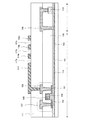
図1は、画素部のスイッチング素子として、トップゲート型薄膜トランジスタ(Thi
n Film Transistor(TFT))を用いた例である。基板101の一方
の表面の全面に、FFS(Fringe−field switching)駆動におけ
る第1の電極となる導電膜115が形成されている。
FIG. 1 shows a top gate thin film transistor (Thi) as a switching element of a pixel portion.
In this example, n Film Transistor (TFT) is used. A
導電膜115として、透光性を有する導電膜(以下「透光性導電膜」という)を用いる
。このような透光性導電膜として、インジウム錫酸化物(Indium Tin Oxi
de(ITO))膜、インジウム亜鉛酸化物(Indium Zinc Oxide(I
ZO))膜、酸化珪素を添加したインジウム錫酸化物(ITSOともいう)膜、酸化亜鉛
(ZnO)膜、酸化スズカドミウム(CTO)膜、酸化スズ(SnO)膜などを用いれば
よい。
As the
de (ITO) film, Indium Zinc Oxide (I
ZO)) film, an indium tin oxide (ITSO) film to which silicon oxide is added, a zinc oxide (ZnO) film, a tin cadmium oxide (CTO) film, a tin oxide (SnO) film, or the like may be used.
導電膜115上には下地膜102、下地膜102上には、薄膜トランジスタ(Thin
Film Transistor(TFT))121が形成されている。TFT121
は、ソース領域またはドレイン領域の一方である領域131a、ソース領域またはドレイ
ン領域の他方である領域131b、チャネル形成領域132を含む活性層103、ゲート
絶縁膜104、ゲート電極105を有している。なお図1ではゲート絶縁膜104は、チ
ャネル形成領域132上部のみに形成されているが、チャネル形成領域132上部以外に
も形成されていてもよい。
A
A film transistor (TFT) 121 is formed. TFT121
Includes a
TFT121及び下地膜102上に、層間絶縁膜106が形成されている。層間絶縁膜
106上には、層間絶縁膜106中のコンタクトホールを介して、ソース領域またはドレ
イン領域の一方に電気的に接続される電極107、ソース領域またはドレイン領域の他方
に電気的に接続される電極108が形成されている。
An interlayer insulating
層間絶縁膜106、電極107〜109上に、層間絶縁膜111が形成されており、さ
らに層間絶縁膜111上に、層間絶縁膜111中に形成されたコンタクトホールを介して
、電極108に電気的に接続される画素電極113及び114a〜114cが形成されて
いる。なお画素電極113は電極108ではなく、電極107に電気的に接続されていて
もよい。また層間絶縁膜106及び111は、いずれか一方のみを形成してもよい。
An interlayer insulating
図1に示すように、画素電極114(114a〜114c)と、画素電極113との間
に電界125が発生する。後述するが、この電界125により液晶分子が駆動される。
As shown in FIG. 1, an
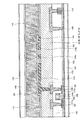
また図3に示すように、導電膜115は、層間絶縁膜106及び下地膜102中のコン
タクトホールを介して、接続電極109と電気的に接続されており、接続電極109は配
線119と電気的に接続されている。なお配線119はゲート電極105と同じ材料、同
じ工程により作製されており、接続電極109は、電極107及び電極108と同じ材料
、同じ工程により作製されている。このように作製工程を追加せずに形成することができ
るため、フォトマスク数を低減させることができる。なお図3と図1に示す構成では同じ
ものは同じ符号で示している。
As shown in FIG. 3, the
なお配線119は、ゲート配線105に平行に配置してもよい。配線119は、ゲート
配線105に平行に配置すると、開口率の低下が小さくなる。
Note that the
また配線119を画素ごとに導電膜115に接続させると、導電膜115の抵抗を小さ
くさせることができる。さらにこの場合は、波形なまりを低減させることができる。
In addition, when the
また接続電極109を配線119に接続させずに、接続電極109を引き延ばして画素
にわたって配置しても構わない。そのときは接続電極109をソース線107と平行に配
置させることが好ましい。
Further, the
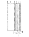
図4に図1及び図3の上面図を示す。図4のA−A’及びB−B’の断面図が図3であ
り、図1は図4のA−A’の断面図である。画素電極113及び114a、114b、1
14c、等には、溝(「開口」、「スリット」、「隙間」、「間隙」、「スペース」とも
いう)117が形成されている。
FIG. 4 shows a top view of FIGS. 1 and 3. 4 is a cross-sectional view taken along line AA ′ and BB ′ in FIG. 4, and FIG. 1 is a cross-sectional view taken along line AA ′ in FIG. 4.
A groove (also referred to as “opening”, “slit”, “gap”, “gap”, “space”) 117 is formed in 14c and the like.
図4に示すように、複数のソース配線107が互いに平行(図中上下方向に延伸)かつ
互いに離間した状態で配置されている。複数のゲート配線105は、ソース配線107に
略直交する方向(図中左右方向)に延伸し、かつ互いに離間するように配置されている。
配線119は、複数のゲート配線105それぞれに隣接する位置に配置されており、ゲー
ト配線105に平行な方向、つまり、ソース配線107に直交する方向(図中左右方向)
に延伸している。このように配置することにより、開口率を向上させることができる。ソ
ース配線107と、配線119及びゲート配線105とによって、略長方形の空間が囲ま
れているが、この空間に液晶表示装置の画素電極113が配置されている。画素電極11
3を駆動する薄膜トランジスタ121は、図中左上の角に配置されている。画素電極及び
薄膜トランジスタは、マトリクス状に複数配置されている。
As shown in FIG. 4, a plurality of source wirings 107 are arranged in parallel with each other (extending in the vertical direction in the drawing) and separated from each other. The plurality of
The
Is stretched. By arranging in this way, the aperture ratio can be improved. A substantially rectangular space is surrounded by the
The
なお本実施の形態では、配線119と導電膜115はコンタクトホールを介して画素ご
とに接続されているが、これに限定されない。
Note that in this embodiment, the
なお、ゲート配線105、配線119、及びソース配線107は、アルミニウム(Al
)、タンタル(Ta)、チタン(Ti)、モリブデン(Mo)、タングステン(W)、ネ
オジウム(Nd)、クロム(Cr)、ニッケル(Ni)、白金(Pt)、金(Au)、銀
(Ag)、銅(Cu)、マグネシウム(Mg)、スカンジウム(Sc)、コバルト(Co
)、亜鉛(Zn)、ニオブ(Nb)、シリコン(Si)、リン(P)、ボロン(B)、ヒ
素(As)、ガリウム(Ga)、インジウム(In)、錫(Sn)、酸素(O)で構成さ
れた群から選ばれた一つもしくは複数の元素、または、前記群から選ばれた一つもしくは
複数の元素を成分とする化合物、合金材料(例えば、インジウム錫酸化物(Indium
Tin Oxide(ITO))、インジウム亜鉛酸化物(Indium Zinc
Oxide(IZO))、酸化珪素を含むインジウム錫酸化物(ITSO)、酸化亜鉛(
ZnO)、酸化錫(SnO)、酸化錫カドミウム(CTO)、アルミネオジウム(Al−
Nd)、マグネシウム銀(Mg−Ag)、モリブデンニオブ(Mo−Nb)など)で形成
されることが望ましい。または、配線、電極、導電層、導電膜、端子などは、これらの化
合物を組み合わせた物質などを有して形成されることが望ましい。もしくは、前記群から
選ばれた一つもしくは複数の元素とシリコンの化合物(シリサイド)(例えば、アルミシ
リコン、モリブデンシリコン、ニッケルシリサイドなど)、前記群から選ばれた一つもし
くは複数の元素と窒素の化合物(例えば、窒化チタン、窒化タンタル、窒化モリブデン等
)を有して形成されることが望ましい。
Note that the
), Tantalum (Ta), titanium (Ti), molybdenum (Mo), tungsten (W), neodymium (Nd), chromium (Cr), nickel (Ni), platinum (Pt), gold (Au), silver (Ag) ), Copper (Cu), magnesium (Mg), scandium (Sc), cobalt (Co
), Zinc (Zn), niobium (Nb), silicon (Si), phosphorus (P), boron (B), arsenic (As), gallium (Ga), indium (In), tin (Sn), oxygen (O Or one or more elements selected from the group consisting of, or a compound or alloy material (for example, indium tin oxide (Indium) containing one or more elements selected from the group as a component)
Tin Oxide (ITO)), Indium Zinc Oxide (Indium Zinc)
Oxide (IZO)), indium tin oxide containing silicon oxide (ITSO), zinc oxide (
ZnO), tin oxide (SnO), tin cadmium oxide (CTO), aluminum neodymium (Al-
Nd), magnesium silver (Mg—Ag), molybdenum niobium (Mo—Nb), and the like. Alternatively, the wiring, the electrode, the conductive layer, the conductive film, the terminal, and the like are preferably formed using a substance in which these compounds are combined. Or one or more elements selected from the group and a silicon compound (silicide) (for example, aluminum silicon, molybdenum silicon, nickel silicide, etc.), one or more elements selected from the group and nitrogen It is desirable to form with a compound (eg, titanium nitride, tantalum nitride, molybdenum nitride, or the like).
なお、シリコン(Si)には、n型不純物(リンなど)またはp型不純物(ボロンなど
)を含んでいてもよい。シリコンが不純物を含むことにより、導電率が向上したり、通常
の導体と同様な振る舞いをすることが可能となる。従って、配線、電極などとして利用し
やすくなる。
Note that silicon (Si) may contain an n-type impurity (such as phosphorus) or a p-type impurity (such as boron). When silicon contains impurities, the conductivity can be improved or the same behavior as a normal conductor can be achieved. Therefore, it becomes easy to use as wiring, electrodes, and the like.
なお、シリコンは、単結晶、多結晶(ポリシリコン)、微結晶(マイクロクリスタルシ
リコン)など、様々な結晶性を有するシリコンを用いることが出来る。あるいは、シリコ
ンは非晶質(アモルファスシリコン)などの結晶性を有さないシリコンを用いることが出
来る。単結晶シリコンまたは多結晶シリコンを用いることにより、配線、電極、導電層、
導電膜、端子などの抵抗を小さくすることが出来る。非晶質シリコンまたは微結晶シリコ
ンを用いることにより、簡単な工程で配線などを形成することが出来る。
Note that silicon having various crystallinity such as single crystal, polycrystal (polysilicon), and microcrystal (microcrystal silicon) can be used. Alternatively, silicon having no crystallinity such as amorphous (amorphous silicon) can be used. By using single crystal silicon or polycrystalline silicon, wiring, electrodes, conductive layers,
Resistance of conductive films, terminals, etc. can be reduced. By using amorphous silicon or microcrystalline silicon, a wiring or the like can be formed by a simple process.
なお、アルミニウムまたは銀は、導電率が高いため、信号遅延を低減することができる
。さらに、エッチングしやすいので、パターニングしやすく、微細加工を行うことが出来
る。
Note that since aluminum or silver has high conductivity, signal delay can be reduced. Further, since etching is easy, patterning is easy and fine processing can be performed.
なお、銅は、導電率が高いため、信号遅延を低減することが出来る。銅を用いる場合は
、密着性を向上させるため、積層構造にすることが望ましい。
Note that since copper has high conductivity, signal delay can be reduced. When copper is used, it is desirable to have a laminated structure in order to improve adhesion.
なお、モリブデンまたはチタンは、酸化物半導体(ITO、IZOなど)またはシリコ
ンと接触しても、不良を起こさない、エッチングしやすい、耐熱性が高いなどの利点を有
するため、望ましい。
Molybdenum or titanium is preferable because it has advantages such as no defects, easy etching, and high heat resistance even when in contact with an oxide semiconductor (ITO, IZO, or the like) or silicon.
なお、タングステンは、耐熱性が高いなどの利点を有するため、望ましい。 Tungsten is desirable because it has advantages such as high heat resistance.
なお、ネオジウムは、耐熱性が高いなどの利点を有するため、望ましい。特に、ネオジ
ウムとアルミニウムとの合金にすると、耐熱性が向上し、アルミニウムがヒロックをおこ
しにくくなる。
Neodymium is desirable because it has advantages such as high heat resistance. In particular, when an alloy of neodymium and aluminum is used, the heat resistance is improved, and aluminum does not easily cause hillocks.
なお、シリコンは、トランジスタが有する半導体層と同時に形成できる、耐熱性が高い
などの利点を有するため、望ましい。
Silicon is preferable because it can be formed at the same time as a semiconductor layer included in a transistor and has high heat resistance.
なお、ITO、IZO、ITSO、酸化亜鉛(ZnO)、シリコン(Si)、酸化錫(
SnO)、酸化錫カドミウム(CTO)は、透光性を有しているため、光を透過させる部
分に用いることができる。たとえば、画素電極や共通電極として用いることができる。
In addition, ITO, IZO, ITSO, zinc oxide (ZnO), silicon (Si), tin oxide (
SnO) and tin cadmium oxide (CTO) have a light-transmitting property, and thus can be used for a portion that transmits light. For example, it can be used as a pixel electrode or a common electrode.
なお、IZOは、エッチングしやすく、加工しやすいため、望ましい。IZOは、エッ
チングしたときに、残渣が残ってしまう、ということも起こりにくい。したがって、画素
電極としてIZOを用いると、液晶素子や発光素子に不具合(ショート、配向乱れなど)
をもたらすことを低減出来る。
Note that IZO is desirable because it is easy to etch and process. It is difficult for IZO to leave a residue when it is etched. Therefore, if IZO is used as the pixel electrode, there is a problem with the liquid crystal element or light emitting element (short circuit, disorder of alignment, etc.)
Can be reduced.
なお、配線、電極、導電層、導電膜、端子などは、単層構造でもよいし、多層構造にな
っていてもよい。単層構造にすることにより、配線、電極、導電層、導電膜、端子などの
製造工程を簡略化することができ、工程日数を少なくでき、コストを低減することが出来
る。あるいは、多層構造にすることにより、それぞれの材料のメリットを生かしつつ、デ
メリットを低減させ、性能の良い配線、電極などを形成することが出来る。たとえば、低
抵抗材料(アルミニウムなど)を多層構造の中に含むことにより、配線の低抵抗化を図る
ことができる。また、低耐熱性の材料を、高耐熱性の材料で挟む積層構造にすることによ
り、低耐熱性の材料の持つメリットを生かしつつ、配線、電極などの耐熱性を高くするこ
とが出来る。例えば、アルミニウムを含む層を、モリブデン、チタン、ネオジウムなどを
含む層で挟む積層構造にすると望ましい。
Note that a wiring, an electrode, a conductive layer, a conductive film, a terminal, or the like may have a single-layer structure or a multilayer structure. With a single-layer structure, a manufacturing process of wiring, electrodes, conductive layers, conductive films, terminals, and the like can be simplified, the number of process days can be reduced, and cost can be reduced. Alternatively, by using a multilayer structure, it is possible to reduce the demerits while making use of the merits of each material, and to form wirings, electrodes, and the like with good performance. For example, by including a low resistance material (such as aluminum) in the multilayer structure, the resistance of the wiring can be reduced. In addition, by using a laminated structure in which a low heat resistant material is sandwiched between high heat resistant materials, the heat resistance of a wiring, an electrode, or the like can be increased while taking advantage of the low heat resistant material. For example, a layered structure in which a layer containing aluminum is sandwiched between layers containing molybdenum, titanium, neodymium, or the like is preferable.
また、配線、電極など同士が直接接する場合、お互いに悪影響を及ぼすことがある。例
えば、一方の配線、電極などが他方の配線、電極など材料の中に入っていって、性質を変
えてしまい、本来の目的を果たせなくなる。別の例として、高抵抗な部分を形成又は製造
するときに、問題が生じて、正常に製造できなくなったりすることがある。そのような場
合、積層構造により反応しやすい材料を、反応しにくい材料で挟んだり、覆ったりすると
よい。例えば、ITOとアルミニウムとを接続させる場合は、ITOとアルミニウムとの
間に、チタン、モリブデン、ネオジウム合金を挟むことが望ましい。また、シリコンとア
ルミニウムとを接続させる場合は、ITOとアルミニウムとの間に、チタン、モリブデン
、ネオジウム合金を挟むことが望ましい。
In addition, when wires, electrodes, etc. are in direct contact with each other, they may adversely affect each other. For example, one wiring, an electrode, or the like enters a material such as the other wiring, an electrode, etc., which changes the properties and cannot fulfill its original purpose. As another example, when a high resistance portion is formed or manufactured, a problem may occur and the manufacturing may not be performed normally. In such a case, it is preferable to sandwich or cover a material that reacts more easily by a laminated structure with a material that does not react easily. For example, when ITO and aluminum are connected, it is desirable to sandwich titanium, molybdenum, or a neodymium alloy between ITO and aluminum. When silicon and aluminum are connected, it is desirable to sandwich titanium, molybdenum, or a neodymium alloy between ITO and aluminum.
なお、配線とは、導電体が配置されているものを言う。線状に伸びていても良いし、伸
びずに短く配置されていてもよい。したがって、電極は、配線に含まれている。
In addition, wiring means what the conductor is arrange | positioned. It may extend linearly or may be arranged short without extending. Therefore, the electrode is included in the wiring.
なお、ゲート配線105の方が、ソース配線107よりも耐熱性が高い材料を用いるこ
とが望ましい。なぜなら、ゲート配線105の方が、製造工程の過程で、高い温度状態に
配置されることが多いからである。
Note that the
なお、ソース配線107の方が、ゲート配線105よりも、抵抗の低い材料を用いるこ
とが望ましい。なぜなら、ゲート配線105には、H信号とL信号の2値の信号を与える
だけであるが、ソース配線107には、アナログの信号を与え、それが表示に寄与するか
らである。よって、ソース配線107には、正確な大きさの信号を供給できるようにする
ため、抵抗の低い材料を用いることが望ましい。
Note that the
なお、配線119を設けなくてもよいが、配線119を設けることにより、各画素にお
ける共通電極の電位を安定化させることができる。なお、図4では、配線119は、ゲー
ト線と平行には配置されているが、これに限定されない。ソース配線107と平行に配置
されていてもよい。その時は、ソース配線107と同じ材質で形成されることが望ましい
。
Note that the
ただし、配線119は、ゲート線と平行には配置したほうが、開口率を大きくすること
ができ、効率的にレイアウトできるため、好適である。
However, it is preferable that the
基板101は、ガラス基板、石英基板、アルミナなど絶縁物で形成される基板、後工程
の処理温度に耐え得る耐熱性を有するプラスチック基板、単結晶基板(単結晶シリコン基
板)、SOI基板、または金属板である。また、多結晶珪素であってもよい。
The
なお、透過型の表示装置として動作させる場合は、基板101は、光透過性を有するこ
とが望ましい。
Note that in the case where the
導電膜115は、光透過性を有する導電膜(例えば、酸化インジウム酸化スズ合金(I
ndium Tin Oxide(ITO)膜、インジウム亜鉛酸化物(Indium
Zinc Oxide(IZOともいう))、酸化亜鉛(ZnO)、酸化スズ(SnO)
、若しくは不純物が導入された多結晶珪素膜又は非晶質珪素膜)から形成されている。
The
ndium Tin Oxide (ITO) film, indium zinc oxide (Indium
Zinc Oxide (also called IZO)), zinc oxide (ZnO), tin oxide (SnO)
, Or a polycrystalline silicon film or an amorphous silicon film into which impurities are introduced.
導電膜115上には、下地膜102として絶縁膜が形成されている。絶縁膜102は、
基板101から不純物が拡散することを防止する膜であり、下地膜として機能する。絶縁
膜102は、例えば、酸化珪素(SiOx)、窒化珪素(SiNx)、窒素を含む酸化珪
素(SiOxNy:x>y)、酸素を含む窒化珪素(SiNxOy:x>y)など、酸素
又は窒素を有する絶縁物質から形成される。また、これらの膜を複数積層した積層膜であ
ってもよい。なお、基板101と導電膜115の間に絶縁膜102と同じ機能を有する絶
縁膜があってもよい。
An insulating film is formed as the
It is a film that prevents impurities from diffusing from the
例えば下地膜102は、窒化珪素膜と酸化珪素膜の積層膜を用いてもよい。また酸化珪
素膜の単層膜でもよい。酸化珪素膜を下地膜102として用いた場合は、ゲート絶縁膜1
04よりも厚くすると、ゲート配線105との容量カップリングを低減できるので有用で
ある。そのため下地膜102は、ゲート絶縁膜104より厚く、望ましくはゲート絶縁膜
104の3倍以上の厚さがあるとよい。
For example, the
When the thickness is larger than 04, it is useful because capacitive coupling with the
絶縁膜102上には半導体膜103が形成されている。半導体膜103には、薄膜トラ
ンジスタ121のソース領域またはドレイン領域の一方となる領域131a、及びソース
領域またはドレイン領域の他方となる領域131bが形成されている。領域131a、1
31bは、例えばn型の不純物領域であるが、p型の不純物領域であってもよい。n型を
付与する不純物としては、例えばリン(P)及びヒ素(As)があり、p型を付与する不
純物としては、例えばボロン(B)及びガリウム(Ga)がある。また領域131aと1
31bとの間にチャネル形成領域132が形成される。
A
31b is, for example, an n-type impurity region, but may be a p-type impurity region. Examples of the impurity imparting n-type include phosphorus (P) and arsenic (As), and examples of the impurity imparting p-type include boron (B) and gallium (Ga).
A
さらに領域131aとチャネル形成領域132との間、領域131bとチャネル形成領
域132との間に、低濃度不純物領域を形成してもよい。
Further, a low concentration impurity region may be formed between the
図4に示すように、導電膜115は画素のほぼ全面に形成されている。ソース配線10
7と、配線119及びゲート配線105とによって囲まれている長方形状の領域には、そ
れぞれ薄膜トランジスタ121が配置されている。すなわち第1の配線としてゲート線1
03、第2の配線としてソース線107、第3の配線として配線119が形成されている
。薄膜トランジスタ121を配置することにより、画素内における表示に有効な領域を、
より効率的に形成することができる。つまり、開口率の向上につながる。なお、半導体膜
103は、例えば多結晶珪素膜であるが、他の半導体膜(例えば非晶質珪素膜、単結晶珪
素膜、有機半導体膜、又はカーボンナノチューブ)、微結晶珪素膜(マイクロクリスタル
シリコン膜、あるいはセミアモルファスシリコン膜ともいう)であってもよい。
As shown in FIG. 4, the
7,
03, a
It can be formed more efficiently. That is, the aperture ratio is improved. The
ここで、セミアモルファスシリコン膜に代表されるセミアモルファス半導体膜とは、非
晶質半導体と結晶構造を有する半導体(単結晶、多結晶を含む)膜の中間的な構造の半導
体を含む膜である。このセミアモルファス半導体膜は、自由エネルギー的に安定な第3の
状態を有する半導体膜であって、短距離秩序を持ち格子歪みを有する結晶質なものであり
、その粒径を0.5〜20nmとして非単結晶半導体膜中に分散させて存在せしめること
が可能である。セミアモルファス半導体膜は、そのラマンスペクトルが520cm−1よ
りも低波数側にシフトしており、またX線回折ではSi結晶格子に由来するとされる(1
11)、(220)の回折ピークが観測される。また、未結合手(ダングリングボンド)
を終端化させるために水素またはハロゲンを少なくとも1原子%またはそれ以上含ませて
いる。本明細書では便宜上、このような半導体膜をセミアモルファス半導体(SAS)膜
と呼ぶ。さらに、ヘリウム、アルゴン、クリプトン、ネオンなどの希ガス元素を含ませて
格子歪みをさらに助長させることで安定性が増し良好なセミアモルファス半導体膜が得ら
れる。
Here, a semi-amorphous semiconductor film typified by a semi-amorphous silicon film is a film containing a semiconductor having an intermediate structure between an amorphous semiconductor and a semiconductor (including single crystal and polycrystal) films having a crystal structure. . This semi-amorphous semiconductor film is a semiconductor film having a third state that is stable in terms of free energy, and is a crystalline film having short-range order and lattice distortion, and has a grain size of 0.5 to 20 nm. And can be dispersed in the non-single-crystal semiconductor film. The semi-amorphous semiconductor film has its Raman spectrum shifted to a lower wave number than 520 cm −1 , and is derived from a Si crystal lattice in X-ray diffraction (1
11) and (220) diffraction peaks are observed. Also, unbonded hands (dangling bonds)
Is contained at least 1 atomic% or more of hydrogen or halogen. In this specification, for convenience, such a semiconductor film is referred to as a semi-amorphous semiconductor (SAS) film. Further, by adding a rare gas element such as helium, argon, krypton, or neon to further promote lattice distortion, stability is improved and a good semi-amorphous semiconductor film can be obtained.
またSAS膜は珪素(シリコン)を含む気体をグロー放電分解することにより得ること
ができる。代表的な珪素(シリコン)を含む気体としては、SiH4であり、その他にも
Si2H6、SiH2Cl2、SiHCl3、SiCl4、SiF4などを用いることが
できる。また水素や、水素にヘリウム、アルゴン、クリプトン、ネオンから選ばれた一種
または複数種の希ガス元素を加えたガスで、この珪素(シリコン)を含む気体を希釈して
用いることで、SAS膜の形成を容易なものとすることができる。希釈率は2倍〜100
0倍の範囲で珪素(シリコン)を含む気体を希釈することが好ましい。またさらに、珪素
(シリコン)を含む気体中に、CH4、C2H6などの炭化物気体、GeH4、GeF4
などのゲルマニウム化気体、F2などを混入させて、エネルギーバンド幅を1.5〜2.
4eV、若しくは0.9〜1.1eVに調節しても良い。
The SAS film can be obtained by glow discharge decomposition of a gas containing silicon. A typical gas containing silicon (Si) is SiH 4 , and Si 2 H 6 , SiH 2 Cl 2 , SiHCl 3 , SiCl 4 , SiF 4, and the like can be used. Further, by diluting and using a gas containing silicon (silicon) with hydrogen or a gas obtained by adding one or more kinds of rare gas elements selected from helium, argon, krypton, or neon to hydrogen, Formation can be facilitated. Dilution rate is 2 to 100
It is preferable to dilute a gas containing silicon (silicon) in a range of 0 times. Further, in a gas containing silicon (silicon), carbide gas such as CH 4 and C 2 H 6 , GeH 4 , GeF 4
A germanium gas such as, such as by mixing the F 2, an energy band width 1.5-2.
You may adjust to 4 eV or 0.9-1.1 eV.
さらにゲート線105の下には半導体層を配置してもよい。これにより導電膜115と
ゲート線105との容量カップリングを低減することができる。そのためゲート線105
の充電及び放電が素早くでき、波形なまりを抑制することができる。
Further, a semiconductor layer may be disposed under the
Can be quickly charged and discharged, and waveform rounding can be suppressed.
半導体膜103上を含む全面上には、薄膜トランジスタ121のゲート絶縁膜104が
形成されている。
A
ただし、ゲート絶縁膜104は、チャネル領域近傍にのみ配置され、それ以外の部分で
は、配置されていない場合もある。また、場所によって厚さや積層構造や厚さが異なる場
合がある。例えば、チャネル近傍のみ厚かったり、層の数が多かったりして、それ以外の
場所では、膜厚が薄かったり、層の数が少ない場合もある。このようにすることにより、
ソース領域やドレイン領域への不純物の添加が制御しやすくなる。また、チャネル近傍の
ゲート絶縁膜104の厚さや層の数を変えることにより、半導体膜への不純物の添加量が
場所によって変わるようにして、LDD領域を形成することが出来る。LDD領域を形成
することにより、漏れ電流を低減したり、ホットキャリアの発生を抑えて信頼性を向上さ
せたりすることが出来る。
However, the
The addition of impurities to the source region and the drain region can be easily controlled. Further, by changing the thickness of the
画素電極113が形成される領域では、ゲート絶縁膜104は形成されなくても構わな
い。画素電極113と導電膜113との間の距離を小さくでき、電界制御がしやすくなる
。
In the region where the
ゲート絶縁膜104は、例えば、酸化珪素(SiOx)、窒化珪素(SiNx)、窒素
を含む酸化珪素(SiOxNy:x>y)、酸素を含む窒化珪素(SiNxOy:x>y
)など、酸素又は窒素を有する絶縁物質から形成される。また、これらの膜を複数積層し
た積層膜であってもよい。ゲート絶縁膜104上には半導体膜103の上方に位置するゲ
ート電極105が形成されている。
The
) Or the like. Further, a laminated film in which a plurality of these films are laminated may be used. A
図4及び図3に示すように、ゲート電極(ゲート配線)105は配線119と同一配線
層である
As shown in FIGS. 4 and 3, the gate electrode (gate wiring) 105 is the same wiring layer as the
ゲート絶縁膜104上及びゲート電極105上には、第1層間絶縁膜106が形成され
ている。第1層間絶縁膜106には、無機材料又は有機材料を用いることができる。有機
材料としては、ポリイミド、アクリル、ポリアミド、ポリイミドアミド、レジスト、シロ
キサン、又はポリシラザンなどを用いることができる。無機材料としては、酸化珪素(S
iOx)、窒化珪素(SiNx)、窒素を含む酸化珪素(SiOxNy:x>y)、酸素
を含む窒化珪素(SiNxOy:x>y)など、酸素又は窒素を有する絶縁物質から形成
される。また、これらの膜を複数積層した積層膜であってもよい。また、有機材料と無機
材料を組み合わせて積層膜にしてもよい。
A first
iO x ), silicon nitride (SiN x ), silicon oxide containing nitrogen (SiO x N y : x> y), silicon nitride containing oxygen (SiN x O y : x> y), etc., insulation having oxygen or nitrogen Formed from material. Further, a laminated film in which a plurality of these films are laminated may be used. Alternatively, a stacked film may be formed by combining an organic material and an inorganic material.
絶縁膜102、ゲート絶縁膜104、及び第1層間絶縁膜106には、領域131a上
に位置するコンタクトホール、領域131b上に位置するコンタクトホール、導電膜11
5上に位置するコンタクトホール、及び配線119上に位置するコンタクトホールが形成
されている。第1層間絶縁膜106上には、ソース配線107、電極108、及び接続用
電極109が形成されている。
In the insulating
A contact hole located on 5 and a contact hole located on the
なお、絶縁膜として無機材料を用いることにより、水分や不純物の侵入を止めることが
出来る。特に、窒素を含む層を用いると、水分や不純物をブロックする機能が高い。
Note that entry of moisture and impurities can be stopped by using an inorganic material for the insulating film. In particular, when a layer containing nitrogen is used, the function of blocking moisture and impurities is high.
なお、絶縁膜として有機材料を用いることにより、表面を平坦にすることが出来る。そ
のため、その上の層に対して、よい効果をもたらすことが出来る。例えば、有機材料の上
に形成する層も平坦にすることが出来るため、液晶の配向の乱れを防いだりすることが出
来る。
Note that the surface can be flattened by using an organic material for the insulating film. Therefore, a good effect can be brought about on the layer above it. For example, since a layer formed over an organic material can be flattened, disorder of alignment of liquid crystals can be prevented.
ソース配線107は領域131aの上方に位置しており、コンタクトホールを介して領
域131aに電気的に接続している。したがって、電極108は、コンタクトホールを介
して領域131bに電気的に接続している。
The
ただし、画素電極113と、不純物領域131bとを、接続用導電膜を介さずに、直接
接続してもよい。この場合、画素電極113と、領域131bとを接続するためのコンタ
クトホールは、深く開ける必要が出てくるが、接続用導電膜が必要ないため、その領域を
開口領域として画像表示に利用できる。そのため、開口率が向上し、低消費電力化をはか
ることが出来る。
However, the
接続電極109は、配線119の上方に位置しており、配線119及び導電膜115そ
れぞれに電気的に接続している。このように、導電膜115は、接続用電極109を介し
て配線119に電気的に接続している。なお、接続用電極109は複数設けられていても
よい。このようにすると、導電膜115の電位が安定化する。また、接続用電極109を
介して導電膜115と配線119を接続することにより、コンタクトホールを形成する回
数を減らすことが出来るので、プロセス工程を簡略化することが出来る。
The
なお、接続用電極109は、ソース配線107と同時に、同じ材料を用いて形成したが
、これに限定されない。画素電極113と同時に、同じ材料を用いて形成してもよい。
Note that although the
ソース配線107、電極108、接続用電極109、及び第1層間絶縁膜106上には
、第2層間絶縁膜111が形成されている。なお、第2層間絶縁膜111を形成しない構
成としても良い(図28参照)。第2層間絶縁膜111には、無機材料又は有機材料を用
いることができる。有機材料としては、ポリイミド、アクリル、ポリアミド、ポリイミド
アミド、レジスト、又はシロキサン、ポリシラザンなどを用いることができる。無機材料
としては、酸化珪素(SiOx)、窒化珪素(SiNx)、窒素を含む酸化珪素(SiO
xNy:x>y)、酸素を含む窒化珪素(SiNxOy:x>y)など、酸素又は窒素を
有する絶縁物質から形成される。また、これらの膜を複数積層した積層膜であってもよい
。また、有機材料と無機材料を組み合わせて積層膜にしてもよい。
A second
xN y : x> y), silicon nitride containing oxygen (SiN x O y : x> y), or the like, formed from an insulating material having oxygen or nitrogen. Further, a laminated film in which a plurality of these films are laminated may be used. Alternatively, a stacked film may be formed by combining an organic material and an inorganic material.
なお第2層間絶縁膜111を形成しないの場合の断面図を、図28に示す。図28中で
、図3と同じものは同じ符号で示している。電極108が形成されないので、画素電極1
13が島状半導体膜103に直接接続されている。ソース配線107、画素電極113及
び画素電極114、並びに接続用電極109は、同じ材料、同じ工程で形成される。図2
8に示す構成では、画素電極113と導電膜105との間隔が小さくでき、電界制御がし
やすくなる。
FIG. 28 shows a cross-sectional view when the second
13 is directly connected to the island-shaped
In the configuration shown in FIG. 8, the distance between the
第2層間絶縁膜111上には、FSS駆動の第2の電極である画素電極113、114
a、114b、114c、等が形成されている。なお断面図である図1及び図3では便宜
上画素電極113と画素電極114(114a、114b、114c、等)を分けている
が、上面図である図4を見れば分かるように、画素電極は、同一材料、同一工程で形成さ
れた導電膜に、溝(「開口」、「スリット」、「隙間」、「間隙」、「スペース」ともい
う)117(117a、117b、117c、等)が形成されているものである。よって
以下の記載においては、画素電極113、114(114a、114b、114c、等)
を、まとめて画素電極113として説明することもある。
On the second
a, 114b, 114c, etc. are formed. In FIG. 1 and FIG. 3 which are cross-sectional views, the
May be collectively described as the
画素電極113は、画素ごとに個別の電圧が供給される画素電極として機能し、ITO
(酸化インジウム酸化スズ合金)、ZnO(酸化亜鉛)、酸化インジウムに2〜20wt
%のZnOを交合したターゲットを用いて形成されたIZO(インジウム亜鉛酸化物)、
酸化スズ(SnO)などによって形成されている。画素電極113は、一部が電極108
の上方に位置しており、電極108に電気的に接続している。このように、画素電極11
3は、電極108を介して薄膜トランジスタ121の領域131bに電気的に接続してい
る。
The
(Indium oxide tin oxide alloy), ZnO (zinc oxide),
% IZO (Indium Zinc Oxide) formed using a target combined with ZnO
It is made of tin oxide (SnO) or the like. A part of the
Is electrically connected to the
3 is electrically connected to the
なお、接続用電極109がない場合は、画素電極113は、薄膜トランジスタ121の
領域131bに直接接続している。
Note that when there is no
図3及び図4に示すように、画素電極113は略長方形であり、複数の溝117a、1
17b、117c、等を有している。溝117a、117b、117c、等の例としては
、スリット状で互いに平行であるものを多く含む。
As shown in FIGS. 3 and 4, the
17b, 117c, etc. Examples of the
図4に示す例では、溝117a、117b、117c、…の向きは、ソース配線107
に対して斜めであるが、画素の図中上半分に位置する溝と、下半分に位置する溝の向きは
互いに異なる。溝117a、117b、117c、…が形成されることにより、導電膜1
15と画素電極113の間で基板に平行な成分を有する電界が、画素電極114のそれぞ
れから導電膜115に向かって生じる。このため、画素電極113及び114の電位を制
御することにより、後述する液晶の配向方向を制御することができる。
In the example shown in FIG. 4, the direction of the
The direction of the grooves located in the upper half of the pixel and the grooves located in the lower half of the pixel are different from each other. By forming the
An electric field having a component parallel to the substrate between 15 and the
また、図4に示されるように、溝117(117a、117b、117c、…)は、向
きが異なるものを配置されている。これによって、液晶分子の動く方向が異なる領域を複
数設けることが出来る。つまり、マルチドメイン構造にすることが出来る。マルチドメイ
ン構造にすることにより、ある特定の方向から見たとき、画像の表示が正しくなくなって
しまうことを防ぐことができ、その結果、視野角を向上させることが出来る。
Further, as shown in FIG. 4, the grooves 117 (117a, 117b, 117c,...) Are arranged in different directions. This makes it possible to provide a plurality of regions in which the liquid crystal molecules move in different directions. That is, it can be a multi-domain structure. By adopting a multi-domain structure, it is possible to prevent the image from being displayed incorrectly when viewed from a specific direction, and as a result, the viewing angle can be improved.
なお、溝の形状は本実施形態の形状に限定されない。溝の形状には、例えば櫛歯形状の
電極における櫛歯部分の相互間のスペース等、導電体が形成されていないスペースを含ま
れるものとする。
The shape of the groove is not limited to the shape of this embodiment. The groove shape includes, for example, a space where no conductor is formed, such as a space between comb teeth in a comb-shaped electrode.
なお画素電極113の厚さと導電膜115の厚さを比較した場合、導電膜115の方が
膜厚が厚い方が好ましい。さらに、より好ましくは導電膜115の方が画素電極113よ
りも1.5倍以上、その膜厚が厚い方が好ましい。こうすることにより、抵抗を低減させ
ることができる。
Note that in the case where the thickness of the
第2層間絶縁膜111上及び画素電極113上には、第1配向膜112及び液晶116
が積層されている。液晶116としては、強誘電性液晶(FLC)、双安定性液晶、ネマ
ティック液晶、スメクティック液晶、高分子分散型液晶、ホモジニアス配向になるような
液晶、ホメオトロピック配向になるような液晶などを用いることができる。また液晶以外
を用いてもよく、例えば電気映像素子等を用いても構わない。液晶116上には、第2配
向膜123及びカラーフィルタ122を介して対向基板120が配置されている。なお、
基板101及び対向基板120それぞれには、偏光板126、124が設けられている。
A
Are stacked. As the
なお、偏光板のほかに、位相差板やλ/4板などが配置されている場合も多い。 In addition to the polarizing plate, a retardation plate, a λ / 4 plate, or the like is often disposed.
なお、上記した構成において、導電膜115、画素電極113のうち溝が形成されてい
ない部分、及びこれらの相互間に位置する各絶縁膜によって、容量が形成される。この容
量が形成されることにより保持容量が大きくなる。
Note that in the above structure, a capacitor is formed by the
次に、本発明の半導体装置、液晶表示装置の製造方法の一例について説明する。まず、
基板101上に透光性を有する導電膜115(例えばインジウム錫酸化物(ITO)、イ
ンジウム亜鉛酸化物(IZO)、酸化亜鉛(ZnO)、酸化スズ(SnO)、又は珪素(
Si))を基板全面に形成する。
Next, an example of a method for manufacturing the semiconductor device and the liquid crystal display device of the present invention will be described. First,
A light-transmitting
Si)) is formed on the entire surface of the substrate.
また図25に示すように、開口部で絶縁膜106を除去しても構わない。さらにあるい
は、ゲート絶縁膜104、下地膜102を除去しても構わない。すなわち、開口部で絶縁
膜106を除去した半導体装置、開口部で絶縁膜106及びゲート絶縁膜104を除去し
た半導体装置、開口部で絶縁膜106、ゲート絶縁膜104、下地膜102を除去した半
導体装置を作製することが可能である。これにより画素電極114と導電膜115との間
隔dを小さくすることができ、その結果、電界制御をしやすくなる。
As shown in FIG. 25, the insulating
次いで、基板101及び導電膜115上それぞれに、絶縁膜102を形成する。絶縁膜
102は、後述するゲート絶縁膜104より厚く形成されることが望ましい。次いで、絶
縁膜102上に半導体膜(例えば多結晶珪素膜)を形成し、この半導体膜を、レジストを
用いたエッチングにより選択的に除去する。これにより、絶縁膜102上には島状の半導
体膜103が形成される。
Next, the insulating
半導体膜は多結晶珪素膜だけでなく、非晶質珪素膜やその他の非単結晶珪素膜を用いて
もよい。また珪素に限定されず、ZnO、a−InGaZnO、SiGe、GaAsなど
の化合物半導体を用いてもよい。
As the semiconductor film, not only a polycrystalline silicon film but also an amorphous silicon film or other non-single-crystal silicon film may be used. Further, the semiconductor is not limited to silicon, and a compound semiconductor such as ZnO, a-InGaZnO, SiGe, or GaAs may be used.
あるいは基板101として半導体基板やSOI(Silicon On Insula
tor)基板を用いて、島状の半導体膜103を形成してもよい。
Alternatively, the
tor) the island-shaped
次いで、半導体膜103上及び絶縁膜102上に、ゲート絶縁膜104を形成する。ゲ
ート絶縁膜104は例えば窒素を含む酸化珪素膜又は酸化珪素膜であり、プラズマCVD
法により形成される。なお、ゲート絶縁膜104を窒化珪素膜、若しくは窒化珪素及び酸
化珪素を有する多層膜により形成してもよい。次いで、ゲート絶縁膜104上に導電膜を
形成し、この導電膜に、エッチングを行うことにより、選択的に除去する。これにより、
半導体膜103上に位置するゲート絶縁膜104上には、ゲート電極105が形成される
。また、本工程により、ゲート配線105及び配線119が形成される。
Next, the
Formed by law. Note that the
A
なお、上記したように配線119を設けることにより、各画素において導電膜115の
電位を安定化させることができる。また、配線119を形成しなくてもよい。また、配線
119を他の層(例えばソース配線107と同一の層、又は導電膜115と同一の層、又
は画素電極113と同一の層)に設けてもよく、複数の層に分けて形成してもよい。また
、本図において配線119は、ソース配線107に直交する方向に延伸しているが、ソー
ス配線107と同一方向に延伸する構成であってもよい。
Note that by providing the
なお、ゲート電極105、配線119を構成する導電膜は、アルミニウム(Al)、タ
ンタル(Ta)、チタン(Ti)、モリブデン(Mo)、タングステン(W)、ネオジウ
ム(Nd)、クロム(Cr)、ニッケル(Ni)、白金(Pt)、金(Au)、銀(Ag
)、銅(Cu)、マグネシウム(Mg)、スカンジウム(Sc)、コバルト(Co)、亜
鉛(Zn)、ニオブ(Nb)、シリコン(Si)、リン(P)、ボロン(B)、ヒ素(A
s)、ガリウム(Ga)、インジウム(In)、錫(Sn)、酸素(O)で構成された群
から選ばれた一つもしくは複数の元素、または、前記群から選ばれた一つもしくは複数の
元素を成分とする化合物、合金材料(例えば、インジウム錫酸化物(ITO)、インジウ
ム亜鉛酸化物(IZO)、酸化珪素を含むインジウム錫酸化物(ITSO)、酸化亜鉛(
ZnO)、酸化錫(SnO)、酸化錫カドミウム(CTO)、アルミネオジウム(Al−
Nd)、マグネシウム銀(Mg−Ag)、モリブデンニオブ(Mo−Nb)など)で形成
されることが望ましい。または、ゲート電極105、配線119を構成する導電膜は、こ
れらの化合物を組み合わせた物質などを有して形成されることが望ましい。もしくは、前
記群から選ばれた一つもしくは複数の元素とシリコンの化合物(シリサイド)(例えば、
アルミシリコン、モリブデンシリコン、ニッケルシリサイドなど)、前記群から選ばれた
一つもしくは複数の元素と窒素の化合物(例えば、窒化チタン、窒化タンタル、窒化モリ
ブデン等)を有して形成されることが望ましい。
Note that the conductive film forming the
), Copper (Cu), magnesium (Mg), scandium (Sc), cobalt (Co), zinc (Zn), niobium (Nb), silicon (Si), phosphorus (P), boron (B), arsenic (A)
s), gallium (Ga), indium (In), tin (Sn), one or more elements selected from the group consisting of oxygen (O), or one or more elements selected from the above group Compounds containing these elements, alloy materials (for example, indium tin oxide (ITO), indium zinc oxide (IZO), indium tin oxide containing silicon oxide (ITSO), zinc oxide (
ZnO), tin oxide (SnO), tin cadmium oxide (CTO), aluminum neodymium (Al-
Nd), magnesium silver (Mg—Ag), molybdenum niobium (Mo—Nb), and the like. Alternatively, the conductive film included in the
(Aluminum silicon, molybdenum silicon, nickel silicide, etc.), and one or more elements selected from the above group and a nitrogen compound (eg, titanium nitride, tantalum nitride, molybdenum nitride, etc.) are preferable. .
なお、シリコン(Si)には、n型不純物(リンなど)またはp型不純物(ボロンなど
)を含んでいてもよい。シリコンが不純物を含むことにより、導電率が向上したり、通常
の導体と同様な振る舞いをすることが可能となる。従って、配線、電極などとして利用し
やすくなる。
Note that silicon (Si) may contain an n-type impurity (such as phosphorus) or a p-type impurity (such as boron). When silicon contains impurities, the conductivity can be improved or the same behavior as a normal conductor can be achieved. Therefore, it becomes easy to use as wiring, electrodes, and the like.
なお、シリコンは、単結晶、多結晶(ポリシリコン)、微結晶(マイクロクリスタルシ
リコン)など、様々な結晶性を有するシリコンを用いることが出来る。あるいは、シリコ
ンは非晶質(アモルファスシリコン)などの結晶性を有さないシリコンを用いることが出
来る。単結晶シリコンまたは多結晶シリコンを用いることにより、配線、電極、導電層、
導電膜、端子などの抵抗を小さくすることが出来る。非晶質シリコンまたは微結晶シリコ
ンを用いることにより、簡単な工程で配線などを形成することが出来る。
Note that silicon having various crystallinity such as single crystal, polycrystal (polysilicon), and microcrystal (microcrystal silicon) can be used. Alternatively, silicon having no crystallinity such as amorphous (amorphous silicon) can be used. By using single crystal silicon or polycrystalline silicon, wiring, electrodes, conductive layers,
Resistance of conductive films, terminals, etc. can be reduced. By using amorphous silicon or microcrystalline silicon, a wiring or the like can be formed by a simple process.
なお、アルミニウムまたは銀は、導電率が高いため、信号遅延を低減することができる
。さらに、エッチングしやすいので、パターニングしやすく、微細加工を行うことが出来
る。
Note that since aluminum or silver has high conductivity, signal delay can be reduced. Further, since etching is easy, patterning is easy and fine processing can be performed.
なお、銅は、導電率が高いため、信号遅延を低減することが出来る。銅を用いる場合は
、密着性を向上させるため、積層構造にすることが望ましい。
Note that since copper has high conductivity, signal delay can be reduced. When copper is used, it is desirable to have a laminated structure in order to improve adhesion.
なお、モリブデンまたはチタンは、酸化物半導体(ITO、IZOなど)またはシリコ
ンと接触しても、不良を起こさない、エッチングしやすい、耐熱性が高いなどの利点を有
するため、望ましい。
Molybdenum or titanium is preferable because it has advantages such as no defects, easy etching, and high heat resistance even when in contact with an oxide semiconductor (ITO, IZO, or the like) or silicon.
なお、タングステンは、耐熱性が高いなどの利点を有するため、望ましい。 Tungsten is desirable because it has advantages such as high heat resistance.
なお、ネオジウムは、耐熱性が高いなどの利点を有するため、望ましい。特に、ネオジ
ウムとアルミニウムとの合金にすると、耐熱性が向上し、アルミニウムがヒロックをおこ
しにくくなる。
Neodymium is desirable because it has advantages such as high heat resistance. In particular, when an alloy of neodymium and aluminum is used, the heat resistance is improved, and aluminum does not easily cause hillocks.
なお、シリコンは、トランジスタが有する半導体層と同時に形成できる、耐熱性が高い
などの利点を有するため、望ましい。
Silicon is preferable because it can be formed at the same time as a semiconductor layer included in a transistor and has high heat resistance.
なお、ITO、IZO、ITSO、酸化亜鉛(ZnO)、シリコン(Si)、酸化錫(
SnO)、酸化錫カドミウム(CTO)は、透光性を有しているため、光を透過させる部
分に用いることができる。たとえば、画素電極や共通電極として用いることができる。
In addition, ITO, IZO, ITSO, zinc oxide (ZnO), silicon (Si), tin oxide (
SnO) and tin cadmium oxide (CTO) have a light-transmitting property, and thus can be used for a portion that transmits light. For example, it can be used as a pixel electrode or a common electrode.
なお、IZOは、エッチングしやすく、加工しやすいため、望ましい。IZOは、エッ
チングしたときに、残渣が残ってしまう、ということも起こりにくい。したがって、画素
電極としてIZOを用いると、液晶素子や発光素子に不具合(ショート、配向乱れなど)
をもたらすことを低減出来る。
Note that IZO is desirable because it is easy to etch and process. It is difficult for IZO to leave a residue when it is etched. Therefore, if IZO is used as the pixel electrode, there is a problem with the liquid crystal element or light emitting element (short circuit, disorder of alignment, etc.)
Can be reduced.
なお、ゲート電極105、配線119を構成する導電膜は、単層構造でもよいし、多層
構造になっていてもよい。単層構造にすることにより、ゲート電極105、配線119を
構成する導電膜の製造工程を簡略化することができ、工程日数を少なくでき、コストを低
減することが出来る。あるいは、多層構造にすることにより、それぞれの材料のメリット
を生かしつつ、デメリットを低減させ、性能の良い配線、電極などを形成することが出来
る。たとえば、低抵抗材料(アルミニウムなど)を多層構造の中に含むことにより、配線
の低抵抗化を図ることができる。また、低耐熱性の材料を、高耐熱性の材料で挟む積層構
造にすることにより、低耐熱性の材料の持つメリットを生かしつつ、配線、電極などの耐
熱性を高くすることが出来る。例えば、アルミニウムを含む層を、モリブデン、チタン、
ネオジウムなどを含む層で挟む積層構造にすると望ましい。
Note that the conductive film included in the
It is desirable to have a laminated structure sandwiched between layers containing neodymium or the like.
また、配線、電極など同士が直接接する場合、お互いに悪影響を及ぼすことがある。例
えば、一方の配線、電極などが他方の配線、電極など材料の中に入っていって、性質を変
えてしまい、本来の目的を果たせなくなる。別の例として、高抵抗な部分を形成又は製造
するときに、問題が生じて、正常に製造できなくなったりすることがある。そのような場
合、積層構造により反応しやすい材料を、反応しにくい材料で挟んだり、覆ったりすると
よい。例えば、ITOとアルミニウムとを接続させる場合は、ITOとアルミニウムとの
間に、チタン、モリブデン、ネオジウム合金を挟むことが望ましい。また、シリコンとア
ルミニウムとを接続させる場合は、ITOとアルミニウムとの間に、チタン、モリブデン
、ネオジウム合金を挟むことが望ましい。
In addition, when wires, electrodes, etc. are in direct contact with each other, they may adversely affect each other. For example, one wiring, an electrode, or the like enters a material such as the other wiring, an electrode, etc., which changes the properties and cannot fulfill its original purpose. As another example, when a high resistance portion is formed or manufactured, a problem may occur and the manufacturing may not be performed normally. In such a case, it is preferable to sandwich or cover a material that reacts more easily by a laminated structure with a material that does not react easily. For example, when ITO and aluminum are connected, it is desirable to sandwich titanium, molybdenum, or a neodymium alloy between ITO and aluminum. When silicon and aluminum are connected, it is desirable to sandwich titanium, molybdenum, or a neodymium alloy between ITO and aluminum.
なお、配線とは、導電体が配置されているものを言う。線状に伸びていても良いし、伸
びずに短く配置されていてもよい。したがって、電極は、配線に含まれている。
In addition, wiring means what the conductor is arrange | positioned. It may extend linearly or may be arranged short without extending. Therefore, the electrode is included in the wiring.
次いで、ゲート電極105をマスクとして、半導体膜103に不純物を注入する。これ
により、半導体膜103には、ソース領域またはドレイン領域の一方である領域131a
、ソース領域またはドレイン領域の他方である131b、及びチャネル形成領域132が
形成される。なお、n型、p型の不純物元素を個別に注入してもよいし、特定の領域には
n型の不純物元素及びp型の不純物元素を共に注入してもよい。ただし後者の場合には、
n型の不純物元素又はp型の不純物元素のどちらか一方の注入量が多くなるようにする。
なお、本工程において、レジストをマスクとして用いてもよい。
Next, impurities are implanted into the
131b, which is the other of the source region and the drain region, and a
The implantation amount of either the n-type impurity element or the p-type impurity element is increased.
Note that a resist may be used as a mask in this step.
なお、このとき、ゲート絶縁膜104の厚さや積層構造を変えることにより、LDD領
域を形成してもよい。LDD領域を形成したい部分は、ゲート絶縁膜104を厚くしたり
、層の数を増やしたりすればよい。その結果、不純物の注入量が減るため、LDD領域を
容易に形成することが出来る。
Note that at this time, the LDD region may be formed by changing the thickness or the stacked structure of the
なお、半導体膜103に不純物を注入する場合、ゲート電極105を形成する前、例え
ば、ゲート絶縁膜104を成膜する前や、成膜した後に行っても良い。その場合は、レジ
ストをマスクとして用いて、形成する。これにより、ゲートと同じレイヤの電極と、不純
物が注入された半導体膜との間で、容量を形成することが出来る。ゲートと同じレイヤの
電極と、不純物が注入された半導体膜との間には、ゲート絶縁膜が配置されているので、
膜厚がうすく、大きな容量を形成することが出来る。
Note that the impurity may be implanted into the
The film thickness is thin and a large capacity can be formed.
次いで、第1層間絶縁膜106を形成し、さらのコンタクトホールを形成する。次いで
、第1層間絶縁膜106上に導電膜(例えば金属膜)を形成し、この導電膜を、マスクを
用いたエッチングにより選択的に除去する。これにより、ソース配線107、電極108
、及び接続電極109が形成される。
Next, a first
And the
次いで、第2層間絶縁膜111を形成し、さらにコンタクトホールを形成する。次いで
、第2層間絶縁膜111上に透光性を有する導電膜(インジウム錫酸化物(ITO)、イ
ンジウム亜鉛酸化物(IZO)、酸化亜鉛(ZnO)、酸化スズ(SnO)、又は珪素(
Si))を形成し、この導電膜を、レジストを用いたエッチングにより選択的に除去する
。これにより、画素電極113が形成される。
Next, a second
Si)) is formed, and the conductive film is selectively removed by etching using a resist. Thereby, the
電極108の一部が充填されているコンタクトホールと、画素電極113の一部が充填
されているコンタクトホールとは位置が同じである場合、1つの場所に収めることが出来
るため、効率的にレイアウトすることが出来る。そのため、画素の開口率を向上させるこ
とができる。
If the contact hole filled with a part of the
一方、電極108の一部が充填されているコンタクトホールと、画素電極113の一部
が充填されているコンタクトホールとは位置が互いに異なっていてもよい。このようにす
ることにより、電極108及び画素電極113のうち、コンタクトホール上に位置する部
分が窪んでも、この窪みが重なることはない。このため、画素電極113に深く窪む部分
が形成されず、上記したレジストのつきまわり不良が発生することを抑制できる。その後
、レジストを除去する。
On the other hand, the contact hole filled with a part of the
次いで、第1配向膜112を形成し、カラーフィルタ122、第2配向膜123が形成
された対向基板120との間に液晶116を封止する。その後、液晶116と接しない側
の対向基板120や基板101に、偏光板126、124、位相差板(図示せず)、λ/
4板等の光学フィルム(図示せず)、拡散板やプリズムシート等の光学フィルム等を設け
る。さらに、バックライトやフロントライトを設ける。バックライトとしては、直下型や
サイドライト型を用いることが出来る。光源としては、冷陰極管やLED(発光ダイオー
ド)を用いることができる。LEDとしては、白色LEDや、色ごとのLED(例えば、
白、赤、青、緑、シアン、マゼンダ、イエローなど)のを組み合わせて用いればよい。L
EDを用いると、光の波長が鋭いため、色純度を上げることが出来る。サイドライト型の
場合は、導光板を配置し、均一な面光源を実現する。このようにして、液晶表示装置が形
成される。
Next, the
An optical film (not shown) such as four plates, an optical film such as a diffusion plate or a prism sheet, and the like are provided. Furthermore, a backlight and a front light are provided. As the backlight, a direct type or a side light type can be used. As the light source, a cold cathode tube or an LED (light emitting diode) can be used. As the LED, a white LED or an LED for each color (for example,
White, red, blue, green, cyan, magenta, yellow, etc.) may be used in combination. L
When ED is used, since the wavelength of light is sharp, color purity can be increased. In the case of the side light type, a light guide plate is arranged to realize a uniform surface light source. In this way, a liquid crystal display device is formed.
なお、液晶表示装置とは、基板と対向基板と、それに挟まれた液晶のみの部分を呼んで
も良い。さらに、液晶表示装置とは、偏光板や位相差板などの光学フィルムを配置したも
のまで含む場合もあり、その他にも、拡散板やプリズムシートや光源(冷陰極管やLED
など)や導光板などを含めてもよい。
Note that the liquid crystal display device may refer to a substrate, a counter substrate, and only a portion of liquid crystal sandwiched therebetween. In addition, the liquid crystal display device may include an optical film such as a polarizing plate or a retardation plate, and in addition, a diffusion plate, a prism sheet, a light source (a cold cathode tube or an LED).
Etc.) or a light guide plate.
また、本実施形態では、チャネル領域の上方にゲート電極を配置した、いわゆるトップ
ゲート型の薄膜トランジスタについて説明をしたが、本発明は特にこれに限定されるもの
ではない。チャネル領域の下方にゲート電極が配置された、いわゆるボトムゲート型の薄
膜トランジスタにしてもよいし、チャネル領域の上下にゲート電極が配置された構造を有
するトランジスタを形成してもよい。
In this embodiment, a so-called top-gate thin film transistor in which a gate electrode is disposed above a channel region has been described, but the present invention is not particularly limited thereto. A so-called bottom-gate thin film transistor in which a gate electrode is disposed below a channel region may be used, or a transistor having a structure in which gate electrodes are disposed above and below a channel region may be formed.
また本実施の形態では、ゲート電極が1つ形成される、いわゆるシングルゲートのTF
Tについて説明したが、ゲート電極が2つ以上形成される、いわゆるマルチゲート型TF
Tを形成してもよい。
In this embodiment mode, a so-called single gate TF in which one gate electrode is formed.
Although T has been described, a so-called multi-gate type TF in which two or more gate electrodes are formed
T may be formed.
また、液晶表示装置は透過型であってもよいし、反射型の液晶表示装置であってもよい
。反射型の液晶表示装置は、例えば導電膜115を光透過性の膜(例えば、インジウム錫
酸化物(ITO)膜、インジウム亜鉛酸化物(IZO)、酸化亜鉛(ZnO)、若しくは
不純物が導入された多結晶珪素膜又は非晶質珪素膜)により形成し、画素電極113を反
射性のある導電膜、例えば金属膜により形成することにより実現できる。また、画素電極
113を光透過性の膜により形成し、かつ導電膜115の一部を反射性のある導電膜、例
えば金属膜により形成して残りを光透過性の膜により形成しても、半透過型の液晶表示装
置を実現できる。
The liquid crystal display device may be a transmissive type or a reflective type liquid crystal display device. In a reflective liquid crystal display device, for example, a light-transmitting film (for example, indium tin oxide (ITO) film, indium zinc oxide (IZO), zinc oxide (ZnO), or impurities) is introduced into the
また反射型の液晶表示装置においては、導電膜115を反射性のある導電膜、例えば金
属膜にすることで、導電膜115に反射板の機能を持たせることができる。画素電極11
3と導電膜115を、両方とも反射性の導電膜を用いることも可能であるし、いずれか一
方を反射性の導電膜にすることも可能である。また基板101と導電膜115の間に絶縁
膜(例えば酸化珪素膜)を設け、この絶縁膜中に反射膜としての金属膜を形成することも
できる。さらに、基板101の外側の面に、反射膜としての反射シート(例えばアルミニ
ウム膜)を設けることもできる。なお、ここで述べた内容は、後述する各実施形態におい
ても同様に適用できる。
In the reflective liquid crystal display device, the
3 and the
本実施の形態により、広い視野角を有しており、かつ従来と比べて製造コストが低い液
晶表示装置を提供することができる。
According to this embodiment, a liquid crystal display device having a wide viewing angle and lower manufacturing cost than the conventional one can be provided.
また本実施の形態では、導電膜を基板全面に形成するので、基板からの不純物が活性層
に混入されるのを防ぐことができる。これにより信頼性の高い半導体装置を得ることが可
能となる。
In this embodiment mode, the conductive film is formed over the entire surface of the substrate, so that impurities from the substrate can be prevented from being mixed into the active layer. As a result, a highly reliable semiconductor device can be obtained.
また本実施の形態では、トップゲート型薄膜トランジスタを有する半導体装置を作製す
るため、バックゲートの電位が安定し、信頼性の高い半導体装置を得ることができる。
In this embodiment mode, a semiconductor device including a top-gate thin film transistor is manufactured; therefore, a highly reliable semiconductor device in which the potential of the back gate is stable can be obtained.
[実施の形態2]
本実施の形態では、画素部のスイッチング素子として、ボトムゲート型TFTを作製し
た例を、図2を用いて説明する。
[Embodiment 2]
In this embodiment, an example in which a bottom gate TFT is manufactured as a switching element in a pixel portion will be described with reference to FIGS.
基板201上に、導電膜202、下地膜203、ゲート電極204、ゲート絶縁膜21
3、活性層となる島状半導体膜206、ソース領域またはドレイン領域の一方である領域
208a、ソース領域またはドレイン領域の他方である領域208b、ソース電極または
ドレイン電極の一方である電極207a、ソース電極またはドレイン電極の他方である電
極207a、画素電極209及び214(214a、214b、214c、等)が形成さ
れている。ゲート電極204、ゲート絶縁膜213、島状半導体膜206、領域208a
、領域208bにより、TFT212が構成されている。
On the
3, an island-shaped
The
電極214と導電膜202との間で横方向電界225が発生する。これにより液晶分子
が駆動される。
A lateral
また下地膜203上には、ゲート電極204と同じ材料、同じ工程で形成された電極2
05が配置されている。絶縁膜210上に形成され、電極209と同じ材料、同じ工程で
形成された電極211が配置されている。電極211は、下地膜203、ゲート絶縁膜2
13、絶縁膜210に形成されたコンタクトホールを介して、導電膜202と電極205
に電気的に接続している。
On the
05 is arranged. An
13, the
Is electrically connected.
基板201は、基板101と同様の材料を用いればよい。
The
導電膜202は、実施の形態1で述べた導電膜115と同様の導電膜を用いればよい。
As the
下地膜203は、下地膜102と同様の材料を用いて形成すればよい。
The
ゲート電極204及び電極205は、ゲート電極105と同様の材料及び同様の工程を
用いて形成すればよい。ゲート絶縁膜213は、ゲート絶縁膜104あるいは絶縁膜10
6と同様の材料で、基板201全面に形成する。
The
6 on the entire surface of the
なお本実施の形態では、ゲート電極が1つ形成される、いわゆるシングルゲートのTF
Tについて説明するが、ゲート電極が2つ以上形成される、いわゆるマルチゲート型TF
Tを形成してもよい。
Note that in this embodiment mode, a so-called single gate TF in which one gate electrode is formed.
T will be described. A so-called multi-gate type TF in which two or more gate electrodes are formed.
T may be formed.
活性層である島状半導体膜206は、島状半導体膜103と同様の材料で形成すればよ
い。好ましくは、アモルファス半導体膜、マイクロクリスタル半導体膜(セミアモルファ
ス半導体膜)が好ましい。その場合は、真性半導体膜(島状半導体膜206)を形成後、
一導電性を付与する不純物を含む半導体膜を形成する。一導電型を付与する不純物は、例
えばn型を付与する不純物であれば、リン(P)、ヒ素(As)等を用いればよく、p型
を付与する不純物としては、ホウ素(B)を用いればよい。本実施の形態のボトムゲート
型TFTはチャネルエッチ型を採用するので、島状半導体膜、ソース電極、ドレイン電極
を形成後、チャネル形成領域の一部にエッチングが必要となる。
The island-shaped
A semiconductor film containing an impurity imparting one conductivity is formed. As the impurity imparting one conductivity type, for example, phosphorus (P), arsenic (As), or the like may be used if it is an impurity imparting n-type, and boron (B) is used as an impurity imparting p-type. That's fine. Since the bottom-gate TFT of this embodiment mode adopts a channel etch type, after forming the island-shaped semiconductor film, the source electrode, and the drain electrode, it is necessary to etch part of the channel formation region.
次いでゲート絶縁膜213及び島状半導体膜206上に、導電膜を形成し、その後一導
電性を付与する不純物を含む半導体膜の一部をエッチングして、領域208a及び208
bを形成する。エッチングにより領域207a及び領域207bを形成する
Next, a conductive film is formed over the
b is formed. The
島状半導体膜206、領域208a、領域208b、電極207a、電極207b上に
は、絶縁膜210が形成される、絶縁膜210は、絶縁膜106あるいは絶縁膜111と
同様の材料、同様の工程を用いて形成すればよい。ただし絶縁膜210として、有機材料
を用いないと、画素電極214と導電膜202との間隔dを小さくすることができ、電界
制御がしやすくなる。
An insulating
絶縁膜210上に、画素電極209及び214(214a、214b、214c、…)
、電極211を形成する。画素電極209及び214は、画素電極113及び114と同
様に、導電膜に溝が形成されたものである。
On the insulating
The
電極211は、ゲート絶縁膜213及び絶縁膜210に形成されたコンタクトホールを
介して、電極205に電気的に接続されている。かつ、下地膜203、ゲート絶縁膜21
3及び絶縁膜210に形成されたコンタクトホールを介して、導電膜202に電気的に接
続されている。
The
3 and the contact hole formed in the insulating
電極208、画素電極209及び214、電極211上には配向膜215が形成される
。配向膜215は、配向膜112と同様の材料を用いて形成すればよい。
An
対向基板221上には、カラーフィルタ222、配向膜223が形成されている。対向
基板221、カラーフィルタ222、配向膜223は、それぞれ対向基板120、カラー
フィルタ122、配向膜123と同様の材料を用いればよい。
On the
対向基板221上の配向膜223、及び基板201上の配向膜215を向かい合わせ、
その空隙に液晶216を注入する。
The
その後、液晶216と接しない側の対向基板221や基板201に、偏光板224、2
17、位相差板(図示せず)、λ/4板等の光学フィルム(図示せず)、拡散板やプリズ
ムシート等の光学フィルム等を設ける。さらに、バックライトやフロントライトを設ける
。バックライトとしては、直下型やサイドライト型を用いることが出来る。光源としては
、冷陰極管やLED(発光ダイオード)を用いることができる。LEDとしては、白色L
EDや、色ごとのLED(例えば、白、赤、青、緑、シアン、マゼンダ、イエローなど)
のを組み合わせて用いればよい。LEDを用いると、光の波長が鋭いため、色純度を上げ
ることが出来る。サイドライト型の場合は、導光板を配置し、均一な面光源を実現する。
このようにして、液晶表示装置が形成される。
Thereafter, the
17. An optical film (not shown) such as a retardation plate (not shown) or a λ / 4 plate, an optical film such as a diffusion plate or a prism sheet, and the like are provided. Furthermore, a backlight and a front light are provided. As the backlight, a direct type or a side light type can be used. As the light source, a cold cathode tube or an LED (light emitting diode) can be used. As LED, white L
ED and LED for each color (for example, white, red, blue, green, cyan, magenta, yellow, etc.)
May be used in combination. When an LED is used, since the wavelength of light is sharp, color purity can be increased. In the case of the side light type, a light guide plate is arranged to realize a uniform surface light source.
In this way, a liquid crystal display device is formed.
また図26に、TFT212の活性層を、結晶性半導体膜で形成した例を示す。なお図
26では、図2と同じものは同じ符号で示している。図26では、TFT212は結晶性
島状半導体膜253を活性層として有しており、結晶性島状半導体膜253は、チャネル
形成領域256、ソース領域またはドレイン領域の一方である領域258a、ソース領域
またはドレイン領域の他方である領域258bを有している。
FIG. 26 shows an example in which the active layer of the
また図26の電極211の代わりに、ソース電極またはドレイン電極の一方である電極
207a及びソース電極またはドレイン電極の他方である電極207bと同じ材料、同じ
工程で形成された電極251を用いる。
In place of the
なお本実施の形態は、実施の形態1のTFT121を、ボトムゲート型TFT212に
変えただけであるので、その他の構成における作製材料や作製工程は、実施の形態1で述
べたものを参照すればよい。
Note that in this embodiment mode, only the
本実施の形態により、広い視野角を有しており、かつ従来と比べて製造コストが低い液
晶表示装置を提供することができる。
According to this embodiment, a liquid crystal display device having a wide viewing angle and lower manufacturing cost than the conventional one can be provided.
本発明では、導電膜を基板全面に形成するので、基板からの不純物が活性層に混入され
るのを防ぐことができる。これにより信頼性の高い液晶表示装置を得ることが可能となる
。
In the present invention, since the conductive film is formed on the entire surface of the substrate, it is possible to prevent impurities from the substrate from being mixed into the active layer. This makes it possible to obtain a highly reliable liquid crystal display device.
[実施の形態3]
本実施の形態は、実施の形態1の電極108を形成せず、画素電極113を直接領域1
31bに接続されるように形成した例を、図6に示す。図6中の符号は実施の形態1のも
のを援用している。その他の構成における作製材料や作製工程は、実施の形態1で述べた
ものを参照すればよい。本実施の形態は、電極108を形成しないので、開口率が高くな
るという利点がある。
[Embodiment 3]
In the present embodiment, the
An example formed so as to be connected to 31b is shown in FIG. The reference numerals in FIG. 6 refer to those in the first embodiment. The materials described in
また必要であれば、実施の形態2で述べたボトムゲート型TFTを援用してもよい。
If necessary, the bottom gate TFT described in
本実施の形態により、広い視野角を有しており、かつ従来と比べて製造コストが低い液
晶表示装置を提供することができる。
According to this embodiment, a liquid crystal display device having a wide viewing angle and lower manufacturing cost than the conventional one can be provided.
本発明では、導電膜を基板全面に形成するので、基板からの不純物が活性層に混入され
るのを防ぐことができる。これにより信頼性の高い液晶表示装置を得ることが可能となる
。
In the present invention, since the conductive film is formed on the entire surface of the substrate, it is possible to prevent impurities from the substrate from being mixed into the active layer. This makes it possible to obtain a highly reliable liquid crystal display device.
また本発明においては、トップゲート型薄膜トランジスタを有する液晶表示装置を作製
した場合、バックゲートの電位が安定するので、信頼性の高い液晶表示装置を得ることが
できる。
In the present invention, when a liquid crystal display device including a top-gate thin film transistor is manufactured, the potential of the back gate is stabilized, so that a highly reliable liquid crystal display device can be obtained.
[実施の形態4]
本実施の形態を、図10、図11、図12、図13を用いて説明する。図10、図11
、図12、図13中の符号は実施の形態1のものを援用している。その他の構成における
作製材料や作製工程は、実施の形態1で述べたものを参照すればよい。
[Embodiment 4]
This embodiment will be described with reference to FIGS. 10, 11, 12, and 13. FIG. 10 and 11
The reference numerals in FIGS. 12 and 13 refer to those in the first embodiment. The materials described in
また必要であれば、実施の形態2で述べたボトムゲート型TFTを援用してもよい。
If necessary, the bottom gate TFT described in
さらに必要であれば、実施の形態3で述べた、画素電極を直接活性層に接続させる構成
を用いてもよい。
If necessary, the structure described in Embodiment 3 in which the pixel electrode is directly connected to the active layer may be used.
図10では、図6の接続電極109に代えて、画素電極113と同様の材料及び同様の
工程で形成された電極141を用いる。配線119及び導電膜115は、電極141を介
して電気的に接続されている。
In FIG. 10, instead of the
また図10の上面図を図11に示す。図11においても図4及び図10と同じものは同
じ符号で示されている。図11中C−C’及びD−D’の断面図が図10である。
A top view of FIG. 10 is shown in FIG. Also in FIG. 11, the same components as those in FIGS. 4 and 10 are denoted by the same reference numerals. FIG. 10 is a cross-sectional view taken along the lines CC ′ and DD ′ in FIG.
また、図12では、図6の接続電極109に代えて、画素電極113と同様の材料及び
同様の工程で形成された電極141、かつ、電極107及び電極108と同様の材料及び
同様の工程で形成された電極142を用いる。配線119及び導電膜115は、電極14
1かつ電極142を介して電気的に接続されている。
In FIG. 12, instead of the
1 and the
また図12の上面図を図13に示す。図13においても図4及び図12と同じものは同
じ符号で示されている。図13中C−C’及びE−E’の断面図が図12である。
A top view of FIG. 12 is shown in FIG. In FIG. 13, the same components as those in FIGS. 4 and 12 are denoted by the same reference numerals. FIG. 12 is a sectional view taken along lines CC ′ and EE ′ in FIG.
本実施の形態により、広い視野角を有しており、かつ従来と比べて製造コストが低い液
晶表示装置を提供することができる。
According to this embodiment, a liquid crystal display device having a wide viewing angle and lower manufacturing cost than the conventional one can be provided.
本発明では、導電膜を基板全面に形成するので、基板からの不純物が活性層に混入され
るのを防ぐことができる。これにより信頼性の高い液晶表示装置を得ることが可能となる
。
In the present invention, since the conductive film is formed on the entire surface of the substrate, it is possible to prevent impurities from the substrate from being mixed into the active layer. This makes it possible to obtain a highly reliable liquid crystal display device.
また本発明においては、トップゲート型薄膜トランジスタを有する液晶表示装置を作製
した場合、バックゲートの電位が安定するので、信頼性の高い液晶表示装置を得ることが
できる。
In the present invention, when a liquid crystal display device including a top-gate thin film transistor is manufactured, the potential of the back gate is stabilized, so that a highly reliable liquid crystal display device can be obtained.
[実施の形態5]
本実施の形態では、画素電極を様々な形状に形成した例を、図7、図8(A)〜図8(
D)、図9(A)〜図9(D)に示す。図7、図8(A)〜図8(D)、図9(A)〜図
9(D)中の符号は実施の形態1のものを援用している。その他の構成における作製材料
や作製工程は、実施の形態1で述べたものを参照すればよい。
[Embodiment 5]
In this embodiment, examples in which pixel electrodes are formed in various shapes are shown in FIGS.
D) and shown in FIGS. 9A to 9D. Reference numerals in FIGS. 7, 8 </ b> A to 8 </ b> D, and 9 </ b> A to 9 </ b> D refer to those in the first embodiment. The materials described in
また必要であれば、実施の形態2で述べたボトムゲート型TFTを援用してもよい。
If necessary, the bottom gate TFT described in
さらに必要であれば、実施の形態3で述べた、画素電極を直接活性層に接続させる構成
を用いてもよい。
If necessary, the structure described in Embodiment 3 in which the pixel electrode is directly connected to the active layer may be used.
またさらに実施の形態4で述べた導電膜115と配線119の接続構造を用いてもよい
。
Further, the connection structure of the
図7は画素電極113を櫛状に形成したものであり、図7における、A−A’及びB−
B’の断面図は図3と同じである。また図8(A)〜図8(B)では、図面の見やすさを
考慮して、画素電極113と導電膜115のみを示している。
FIG. 7 shows the
The cross-sectional view of B ′ is the same as FIG. In FIGS. 8A to 8B, only the
図8(A)において画素電極113には、スリット状の開口がそれぞれ複数形成されて
いる。スリット状の開口はソース配線に対して斜めである。かつ、画素電極113の上半
分に形成されているスリット状の開口と、画素電極113の下半分に形成されているスリ
ット状の開口は、画素電極113の中心線に対して互いの角度が異なる。画素電極113
の上半分に形成されているスリット状の開口と、画素電極113の下半分に形成されてい
るスリット状の開口は、中心線に対して線対称であってもよい。
In FIG. 8A, the
The slit-like opening formed in the upper half of the pixel electrode and the slit-like opening formed in the lower half of the
図8(B)において、画素電極113は、それぞれが円周に沿う形状を有していて半径
が異なる複数の電極を同心に配置し、これらを接続した形状である。そして、各電極の相
互間のスペースが、開口の役割を果たしている。
In FIG. 8B, the
図8(C)において、画素電極113は、櫛歯状の2つの電極を、逆向きかつ櫛歯部分
が互い違いになるように配置したものである。そして櫛歯部分の相互間に位置するスペー
スが開口の役割を果たしている。
In FIG. 8C, a
図8(D)において、画素電極113は櫛歯状の形状を有しており、櫛歯部分の相互間
に位置するスペースが開口の役割を果たしている。
In FIG. 8D, the
図9(A)において、画素電極113は斜めの方向にストライプ状であり、ストライプ
状部分の相互間に位置するスペースが開口の役割を果たしている。
In FIG. 9A, the
図9(B)において、画素電極113には矩形状の開口部が複数形成されている。
In FIG. 9B, a plurality of rectangular openings are formed in the
図9(C)において、画素電極113中に、細長い長方形の互いに向かい合う二辺が波
状である開口部が形成されている。
In FIG. 9C, in the
図9(D)において、画素電極113中に、細長い長方形状の開口部が形成されている
。
In FIG. 9D, an elongated rectangular opening is formed in the
本発明により、広い視野角を有しており、かつ従来と比べて製造コストが低い液晶表示
装置を提供することができる。
According to the present invention, it is possible to provide a liquid crystal display device having a wide viewing angle and having a lower manufacturing cost than the conventional one.
本発明では、導電膜を基板全面に形成するので、基板からの不純物が活性層に混入され
るのを防ぐことができる。これにより信頼性の高い液晶表示装置を得ることが可能となる
。
In the present invention, since the conductive film is formed on the entire surface of the substrate, it is possible to prevent impurities from the substrate from being mixed into the active layer. This makes it possible to obtain a highly reliable liquid crystal display device.
また本発明においては、トップゲート型薄膜トランジスタを有する液晶表示装置を作製
した場合、バックゲートの電位が安定するので、信頼性の高い液晶表示装置を得ることが
できる。
In the present invention, when a liquid crystal display device including a top-gate thin film transistor is manufactured, the potential of the back gate is stabilized, so that a highly reliable liquid crystal display device can be obtained.
[実施の形態6]
本実施の形態では、実施の形態1と異なる場所にカラーフィルタを設けた例について、
図22、図23(A)〜図23(B)、図24を用いて説明する。
[Embodiment 6]
In this embodiment, an example in which a color filter is provided in a place different from that in
This will be described with reference to FIGS. 22, 23A to 23B, and FIG.
図22は、本実施の形態に係るFFS方式の液晶表示装置の画素部の構成を説明する為
の断面図である。本実施の形態に係る液晶表示装置の画素部は、対向基板120側にカラ
ーフィルタを配置せず、層間絶縁膜106の代わりにカラーフィルタ241(赤色のカラ
ーフィルタ241R、青色のカラーフィルタ241B、及び緑色のカラーフィルタ241
G)を配置した点を除いて、実施の形態1に示した液晶表示装置と同様の構成である。
FIG. 22 is a cross-sectional view for explaining the structure of the pixel portion of the FFS mode liquid crystal display device according to this embodiment. The pixel portion of the liquid crystal display device according to this embodiment does not include a color filter on the
The configuration is the same as that of the liquid crystal display device described in
従って、実施の形態1以外の他の実施の形態で説明した内容は、本実施形態においても適
用できる。以下、実施の形態1と同様の構成については同一の符号を付し、説明を省略す
る。
Therefore, the contents described in other embodiments than the first embodiment can be applied to this embodiment. Hereinafter, the same components as those of the first embodiment are denoted by the same reference numerals, and description thereof is omitted.
なお、カラーフィルタ241とゲート電極105との間に、無機材料の絶縁膜を配置し
てもよい。無機材料としては、酸化珪素、窒化珪素、窒素を含む酸化珪素、酸素を含む窒
化珪素など、酸素又は窒素を有する絶縁物質から形成される。不純物の侵入をブロックす
るためには、窒素を多く含む材料にすることが望ましい。また、カラーフィルタ241上
に、平坦化膜を形成してもよい。
Note that an insulating film of an inorganic material may be provided between the color filter 241 and the
なお、カラーフィルタ241の色は、赤、青、緑以外の色でも良いし、3色よりも多く
、例えば、4色や6色でもよい。例えば、イエローやシアンやマゼンダや白が追加されて
よい。また、カラーフィルタだけでなく、ブラックマトリックスも配置してもよい。さら
に、ブラックマトリクスは、樹脂材料で形成しても、金属膜で形成しても構わない。さら
にブラックマトリクスは、カーボンブラックを用いて形成しても構わない。
The color of the color filter 241 may be a color other than red, blue, and green, or more than three colors, for example, four or six colors. For example, yellow, cyan, magenta, and white may be added. Further, not only a color filter but also a black matrix may be arranged. Further, the black matrix may be formed of a resin material or a metal film. Further, the black matrix may be formed using carbon black.
このように、基板101上にカラーフィルタ241を配置することにより、対向基板1
20との位置合わせを正確にやる必要がないため、容易に製造することが可能となり、コ
ストが低減し、製造歩留まりが向上する。
Thus, by disposing the color filter 241 on the
Since it is not necessary to accurately align the position 20, manufacturing can be easily performed, cost is reduced, and manufacturing yield is improved.
本実施の形態に係る液晶表示装置の製造方法は、層間絶縁膜106を形成する工程の代
わりにカラーフィルタ241(241R、241G、241B)を形成する工程が入る点
を除いて、実施の形態1に係る液晶表示装置の製造方法と同様である。
The manufacturing method of the liquid crystal display device according to this embodiment is the same as that in
カラーフィルタ241R、241G、241Bは、カラーフィルタ層を形成する工程、
カラーフィルタ層上にレジストを形成する工程、及びレジストをマスクとしてカラーフィ
ルタ層を選択的にドライエッチングする工程を3回繰り返すことにより形成される。
The color filters 241R, 241G, and 241B are steps for forming a color filter layer,
It is formed by repeating a step of forming a resist on the color filter layer and a step of selectively dry-etching the color filter layer using the resist as a mask three times.
または、レジストを用いずに、感光性の材料や顔料などを用いて形成される。なお、カ
ラーフィルタ層相互間にスペースが生じるが、このスペースには層間絶縁膜111が埋め
込まれる。あるいは、さらに無機材料や有機材料が、積層される。あるいは、ブラックマ
トリックスなどが積層される。また、カラーフィルタ241R、241G、241Bやブ
ラックマトリックスは液滴吐出法(例えばインクジェット法)を用いても形成することが
できる。
Alternatively, it is formed using a photosensitive material or a pigment without using a resist. Note that a space is generated between the color filter layers, and the
このため、液晶表示装置の製造工程数を減らすことができる。また、基板101側にカ
ラーフィルタを設けているため、対向基板120にカラーフィルタを設ける場合と比較し
て、対向基板120との間に位置ずれが生じても開口率が低下することを抑制できる。す
なわち対向基板120の位置ずれに対するマージンが大きくなる。
For this reason, the number of manufacturing steps of the liquid crystal display device can be reduced. In addition, since the color filter is provided on the
図23(A)は、図22に示した液晶表示装置の平面図である。図23(A)に示すよ
うに、本実施の形態の液晶表示装置は、画素部150の周囲に、周辺駆動回路であるソー
ス線駆動回路152及びゲート線駆動回路154が設けられている。
FIG. 23A is a plan view of the liquid crystal display device shown in FIG. As shown in FIG. 23A, in the liquid crystal display device in this embodiment, a source
ソース線駆動回路152及びゲート線駆動回路154それぞれ上には、赤色のカラーフ
ィルタ241Rが設けられていてもよい。カラーフィルタ241Rが設けられることによ
り、ソース線駆動回路152及びゲート線駆動回路154が有する薄膜トランジスタの活
性層の光劣化が防止され、かつ平坦化が図られている。
A
図23(B)は、図23(A)の画素部150の一部(3×3行列)を拡大した図であ
る。画素部150には、赤色のカラーフィルタ241R、青色のカラーフィルタ241B
、及び緑色のカラーフィルタ241Gがストライプ状に交互に配置されている。また、各
画素が有する薄膜トランジスタ上には赤色のカラーフィルタ241Rが配置されている。
FIG. 23B is an enlarged view of a part (3 × 3 matrix) of the pixel portion 150 in FIG. The pixel portion 150 includes a
And
また、ソース配線(図示せず)及びゲート配線(図示せず)は、各カラーフィルタの相
互間のスペースと重なるように配置されているため、光漏れが生じることが抑制される。
Further, since the source wiring (not shown) and the gate wiring (not shown) are arranged so as to overlap with the space between the color filters, the occurrence of light leakage is suppressed.
このようにカラーフィルタ241Rはブラックマトリックスの役割を果たすため、従来
必要であったブラックマトリックスの形成工程を省略することも可能である。
As described above, since the
以上、本実施の形態によれば、他の実施の形態と同様の効果を得ることができる。また
、層間絶縁膜106の代わりにカラーフィルタ241R、241G、241Bを設けたた
め、液晶表示装置の製造工程数を減らすことができる。また、対向基板120にカラーフ
ィルタを設ける場合と比較して、対向基板120との間に位置ずれが生じても、開口率の
低下が抑制できる。すなわち対向基板120の位置ずれに対するマージンが大きくなる。
As described above, according to the present embodiment, the same effects as those of the other embodiments can be obtained. In addition, since the
また、カラーフィルタだけでなく、ブラックマトリックスも配置してもよい。 Further, not only a color filter but also a black matrix may be arranged.
なお、他の実施の形態で示したFFS方式の液晶表示装置において、本実施の形態と同
様に、層間絶縁膜106や、あるいは第2層間絶縁膜111の代わりに(図24参照)、
カラーフィルタ241(241R、241G、241B)を設けてもよい。この場合にお
いても、本実施の形態と同様の効果を得ることができる。
Note that in the FFS mode liquid crystal display device described in another embodiment, instead of the
Color filters 241 (241R, 241G, 241B) may be provided. Even in this case, the same effect as the present embodiment can be obtained.
[実施の形態7]
本実施形態においては、表示装置の表示パネル構成、および周辺構成について説明する
。特に、液晶表示装置の表示パネル(液晶パネルとも記す)構成、および周辺構成につい
て説明する。
[Embodiment 7]
In the present embodiment, a display panel configuration and a peripheral configuration of the display device will be described. In particular, a display panel (also referred to as a liquid crystal panel) configuration and a peripheral configuration of a liquid crystal display device will be described.
まず、液晶パネルの簡単な構成について、図29(A)を参照して説明する。また、図
29(A)は、液晶パネルの上面図である。
First, a simple structure of the liquid crystal panel will be described with reference to FIG. FIG. 29A is a top view of the liquid crystal panel.
図29(A)に示す液晶パネルは、基板20100上に、画素部20101、走査線側
入力端子20103及び信号線側入力端子20104が形成されている。走査線側入力端
子20103から走査線が行方向に延在して基板20100上に形成され、信号線入力端
子20104から信号線が列方向に延在して基板20100上に形成されている。また、
画素部20101には、画素20102が走査線と、信号線とが交差するところで、マト
リクス上に配置されている。また、画素20102には、スイッチング素子と画素電極層
とが配置されている。
In the liquid crystal panel illustrated in FIG. 29A, a
In the
図29(A)の液晶パネルに示すように、走査線側入力端子20103は、基板201
00の行方向の両側に形成されている。信号線入力端子20103は、基板20100の
列方向のうち一方に形成されている。また、一方の走査線側入力端子20103から延在
する走査線と、他方の走査線側入力端子20103から延在する走査線とは、交互に形成
されている。
As shown in the liquid crystal panel in FIG. 29A, the scan line
00 is formed on both sides in the row direction. The signal
また、画素部20101の画素20102それぞれでは、スイッチング素子の第1端子
が信号線に接続され、第2端子が画素電極層に接続されることによって、個々の画素20
102を外部から入力する信号によって独立して制御することができる。なお、スイッチ
ング素子のオン・オフは走査線に供給されている信号によって制御されている。
In each
102 can be independently controlled by a signal input from the outside. Note that on / off of the switching element is controlled by a signal supplied to the scanning line.
なお、走査線側入力端子20103を基板20100の行方向のうち両方に配置するこ
とで、画素20102を高密度に配置することができる。また、信号線側入力端子201
03を基板20100の列方向のうち一方に配置することで、液晶パネルの狭額縁化、又
は画素20101の領域の拡大を図ることができる。
Note that the
By arranging 03 in one of the column directions of the
なお、基板20100には、すでに述べたように、単結晶基板、SOI基板、ガラス基
板、石英基板、プラスチック基板、紙基板、セロファン基板、石材基板、ステンレス・ス
チル基板、ステンレス・スチル・ホイルを有する基板などを用いることができる。
Note that as described above, the
なお、スイッチング素子には、すでに述べたように、トランジスタ、ダイオード(例え
ば、PNダイオード、PINダイオード、ショットキーダイオード、ダイオード接続のト
ランジスタなど)、サイリスタ、それらを組み合わせた論理回路などを用いることができ
る。
Note that as described above, a transistor, a diode (for example, a PN diode, a PIN diode, a Schottky diode, a diode-connected transistor, or the like), a thyristor, or a logic circuit combining them can be used as the switching element. .
なお、スイッチング素子として、TFTを用いた場合、TFTのゲートが走査線に接続
され、第1端子が信号線に接続され、第2端子が画素電極層に接続されることにより、個
々の画素20102を外部から入力する信号によって独立して制御することができる。
Note that in the case where a TFT is used as the switching element, the gate of the TFT is connected to the scanning line, the first terminal is connected to the signal line, and the second terminal is connected to the pixel electrode layer. Can be controlled independently by an externally input signal.
なお、走査線側入力端子20103を基板20100の行方向のうち一方に配置しても
よい。走査線側入力端子20103を基板20100の行方向のうち一方に配置すること
で、液晶パネルの狭額縁化、画素20101の領域の拡大を図ることができる。
Note that the scan line
なお、一方の走査線側入力端子20103から延在する走査線と、他方の走査線側入力
端子20103から延在する走査線とは、共通にしてもよい。
Note that the scanning line extending from one scanning line
なお、信号線側入力端子20103を基板20100の列方向のうち両方に配置しても
よい。信号線側入力端子20103を基板20100の列方向のうち両方に配置すること
で、画素20102を高密度に配置できる。
Note that the signal line
なお、画素20102には、さらに容量素子を形成してもよい。画素20102に容量
素子を設ける場合、基板20100上に、容量線を形成してもよい。基板20100上に
容量線を形成する場合、容量素子の第1電極が容量線に接続され、第2端子が画素電極層
に接続されるようにする。また、基板20100上に容量線を形成しない場合、容量素子
の第1電極がこの容量素子が配置されている画素20102とは別の走査線に接続され、
第2端子が画素電極層に接続されているようにする。
Note that a capacitor may be further formed in the
The second terminal is connected to the pixel electrode layer.
ここで、図29(A)に示した液晶パネルは、走査線及び信号線に供給する信号を外付
けの駆動回路によって制御する構成を示しているが、図30(A)に示すように、COG
(Chip on Glass)方式によりドライバIC20201を基板20100上
に実装してもよい。また、別の構成として、図30(B)に示すように、TAB(Tap
e Automated Bonding)方式によりドライバIC20201をFPC
(Flexible Printed Circuit)20200上に実装してもよい
。また、図30において、ドライバIC20201は、FPC20200と接続されてい
る。
Here, the liquid crystal panel illustrated in FIG. 29A illustrates a configuration in which signals supplied to the scan lines and the signal lines are controlled by an external driver circuit. As illustrated in FIG. COG
The
e Auto Bonding)
(Flexible Printed Circuit) 20200 may be implemented. In FIG. 30, the
なお、ドライバIC20201は単結晶半導体基板上に形成されたものでもよいし、ガ
ラス基板上にTFTで回路を形成したものでもよい。
Note that the
なお、図29(A)に示した液晶パネルは、図29(B)に示すように、走査線駆動回
路20105を基板20100上に形成してもよい。また、図29(C)に示すように、
走査線駆動回路20105及び信号線駆動回路20106を基板20100上に形成して
もよい。
Note that in the liquid crystal panel illustrated in FIG. 29A, the scan
The scan
なお、走査線駆動回路20105及び走査線駆動回路20106は、多数のNチャネル
型及び多数のPチャネル型のトランジスタから構成されている。ただし、多数のNチャネ
ル型のトランジスタのみで構成されていてもよいし、多数のPチャネル型のトランジスタ
のみで構成されていてもよい。
Note that the scan
続いて、画素20102の詳細について、図31及び図32の回路図を参照して説明す
る。
Next, details of the
図31(A)の画素20102は、トランジスタ20301、液晶素子20302及び
容量素子20303を有している。トランジスタ20301のゲートが配線20305に
接続され、第1端子が配線20304に接続されている。液晶素子20302の第1電極
が対向電極20307に接続され、第2電極がトランジスタ20301の第2端子に接続
されている。容量素子20303の第1電極が配線20306に接続され、第2電極がト
ランジスタ20301の第2端子に接続されている。
A
なお、配線20304は信号線であり、配線20305は走査線であり、配線2030
6は容量線である。また、トランジスタ20301は、スイッチングトランジスタであり
、Pチャネル型トランジスタでもNチャネル型トランジスタでもよい。また、液晶素子2
0307は、動作モードとしてTN(Twisted Nematic)モード、IPS
(In−Plane−Switching)モード、FFS(Fringe Field
Switching)モード、MVA(Multi−domain Vertical
Alignment)モード、PVA(Patterned Vertical Al
ignment)、ASM(Axially Symmetric aligned M
icro−cell)モード、OCB(Optical Compensated Bi
refringence)モード、FLC(Ferroelectric Liquid
Crystal)モード、AFLC(AntiFerroelectric Liqu
id Crystal)などを用いることができる。
Note that the
6 is a capacity line. The
0307 is a TN (Twisted Nematic) mode as an operation mode, IPS
(In-Plane-Switching) mode, FFS (Fringe Field)
Switching mode, MVA (Multi-domain Vertical)
Alignment mode, PVA (Patterned Vertical Al)
ignition), ASM (Axial Symmetric aligned M)
micro-cell) mode, OCB (Optical Compensated Bi)
refrenceence) mode, FLC (Ferroelectric Liquid)
Crystal) mode, AFLC (Antiferroelectric Liquid)
id Crystal) or the like can be used.
配線20304及び配線20305には、それぞれビデオ信号、走査信号が入力されて
いる。ビデオ信号はアナログの電圧信号であり、走査信号はHレベル又はLレベルのデジ
タルの電圧信号である。ただし、ビデオ信号は電流信号でもよいし、デジタル信号でもよ
い。また、走査信号のHレベル及びLレベルは、トランジスタ20301のオン・オフを
制御できる電位であればよい。
A video signal and a scanning signal are input to the
容量線20306には、一定の電源電圧が供給されている。ただし、パルス状の信号が
供給されていてもよい。
A constant power supply voltage is supplied to the
図31(A)の画素20102の動作について説明する。まず、配線20305がHレ
ベルになると、トランジスタ20301がオンし、ビデオ信号が配線20304からオン
したトランジスタ20301を介して液晶素子20302の第2電極及び容量素子203
03の第2電極に供給される。そして、容量素子20303は配線203076の電位と
ビデオ信号の電位との電位差を保持する。
The operation of the
03 is supplied to the second electrode. The
次に、配線20305がLレベルになると、トランジスタ20301がオフし、配線2
0304と、液晶素子20302の第2電極及び容量素子20303の第2電極とは、電
気的に遮断される。しかし、容量素子20303が配線203076の電位とビデオ信号
の電位との電位差を保持しているため、容量素子20302の第2電極の電位はビデオ信
号と同様な電位を維持することができる。
Next, when the
0304 is electrically disconnected from the second electrode of the
こうして、図31(A)の画素20102は、液晶素子20302の第2電極の電位を
ビデオ信号と同電位に維持でき、液晶素子20302をビデオ信号に応じた透過率に維持
できる。
In this manner, the
なお、図示はしないが、液晶素子20302がビデオ信号を保持できるたけの容量成分
を有していれば、容量素子20303は必ずしも必要ではない。
Note that although not illustrated, the
なお、図31(B)のように、液晶素子20302の第1電極は、配線20306と接
続されていてもよい。例えば、液晶素子20302の液晶モードがFFSモードのときな
どに、液晶素子20302は図31(B)の構成を用いる。
Note that the first electrode of the
なお、図32のように、容量素子20303の第1電極は前行の配線20305aに接
続されていてもよい。なお、配線20305aをn行目(nは正の整数)の走査線とした
とき、配線20305bはn+1行目の走査線である。同様に、トランジスタ20301
a、画素20102a、容量素子20303aをn行目の素子としたとき、トランジスタ
20301b、画素20102b、容量素子20303bはn+1行目の素子である。こ
のように、容量素子20303bの第1電極が前列の配線20305aに接続されること
で、配線を少なくすることができる。よって、図32の画素20102aおよび2010
2bは、開口率を大きくすることができる。
Note that as shown in FIG. 32, the first electrode of the
a, when the
2b can increase the aperture ratio.
次に、図33に示した液晶表示装置には、バックライトユニット22601、液晶パネ
ル22607、第1の偏光子を含む層22608、第2の偏光子を含む層22609が設
けられている。
Next, the liquid crystal display device illustrated in FIG. 33 is provided with a
なお、液晶パネル22607は、本実施形態で説明したものと同様なものとすることが
できる。また、本実施形態の液晶パネルは、各画素にスイッチング素子が設けられたアク
ティブ型の構造について説明してきたが、図33の液晶パネルはパッシブ型の構造でもよ
い。
Note that the
バックライトユニット22601の構造について説明する。バックライトユニット22
601は、拡散板22602、導光板22603、反射板22604、ランプリフレクタ
22605、光源22606を有するように構成されている。光源22606としては冷
陰極管、熱陰極管、発光ダイオード、無機EL又は有機ELなどが用いられ、光源226
06は必要に応じて発光する機能を有する。ランプリフレクタ22605は、光源226
06からの蛍光を効率よく導光板22603に導く機能を有する。導光板22603は、
蛍光を全反射させて、全面に光を導く機能を有する。拡散板22602は、明度のムラを
低減する機能を有する。反射板22604は、導光板22603から下方向(液晶パネル
22607と反対方向)に漏れた光を反射して再利用する機能を有する。
The structure of the
601 is configured to include a
06 has a function of emitting light as necessary. The
It has a function of efficiently guiding the fluorescence from 06 to the
It has a function of totally reflecting fluorescence and guiding light to the entire surface. The
なお、拡散板22602と第2の偏光子を含む層22609との間に、プリズムシート
を配置することで、本実施形態の液晶表示装置は液晶パネルの画面の明るさを向上させる
ことができる。
In addition, the liquid crystal display device of this embodiment can improve the brightness of the screen of a liquid crystal panel by arrange | positioning a prism sheet between the
バックライトユニット22601には、光源22606の輝度を調整するための制御回
路が接続されている。制御回路からの信号供給によって、光源22606の輝度を調整す
ることができる。
A control circuit for adjusting the luminance of the
液晶パネル22607とバックライトユニット22601との間には第2の偏光子を含
む層22609が設けれ、バックライトユニット22601とは反対方向の液晶パネル2
2607にも第1の偏光子を含む層22608が設けられている。
A
A
なお、第1の偏光子を含む層22608と第2の偏光子を含む層22609とは、液晶
パネル22607の液晶素子がTNモードで駆動する場合、クロスニコルになるように配
置される。また、第1の偏光子を含む層22608と第2の偏光子を含む層22609と
は、液晶パネル22607の液晶素子がVAモードで駆動する場合、クロスニコルになる
ように配置される。また、第1の偏光子を含む層22608と第2の偏光子を含む層22
609とは、液晶パネル22607の液晶素子がIPSモード及びFFSモードで駆動す
る場合、クロスニコルになるように配置されていてもよいし、パラレルニコルになるよう
に配置されていてもよい。
Note that the
When the liquid crystal element of the
第1の偏光子を含む層22608及び第2の偏光子を含む層22609の両方又は一方
と、液晶パネル22607との間に位相差板を有していてもよい。
A retardation plate may be provided between both or one of the
なお、図36に示すように、第2の偏光子を含む層22609とバックライトユニット
22601との間に、スリット(格子)22610を配置することで、本実施形態の液晶
表示装置は3次元表示を行うことができる。
As shown in FIG. 36, the slit (grating) 22610 is disposed between the
バックライトユニット側に配置された開口部を有するスリット22610は、光源より入
射された光をストライプ状にして透過し、表示装置へ入射させる。このスリット2261
0によって、視認側にいる視認者の両目に視差を作ることができ、視認者は右目では右目
用の画素だけを、左目では左目用の画素だけを同時に見ることになる。よって、視認者は
、3次元表示を見ることができる。つまり、スリット22610によって特定の視野角を
与えられた光が右目用画像及び左目用画像のそれぞれに対応する画素を通過することで、
右目用画像と左目用画像とが異なる視野角に分離され、3次元表示が行われる。
A slit 22610 having an opening disposed on the backlight unit side transmits light incident from the light source in a stripe shape and allows the light to enter the display device. This slit 2261
With 0, parallax can be created in both eyes of the viewer on the viewer side, and the viewer sees only the pixels for the right eye in the right eye and only the pixels for the left eye in the left eye. Therefore, the viewer can see the three-dimensional display. That is, the light given a specific viewing angle by the slit 22610 passes through pixels corresponding to the right-eye image and the left-eye image,
The right-eye image and the left-eye image are separated into different viewing angles, and three-dimensional display is performed.
図36の液晶表示装置を用いて、テレビジョン装置、携帯電話などの電子機器を作製す
れば、3次元表示を行うことができる高機能でかつ高画質の電子機器を提供することがで
きる。
When an electronic device such as a television device or a mobile phone is manufactured using the liquid crystal display device in FIG. 36, a high-function and high-quality electronic device that can perform three-dimensional display can be provided.
続いて、バックライトの詳細な構成について、図35を参照して説明する。バックライ
トは光源を有するバックライトユニットとして液晶表示装置に設けられ、バックライトユ
ニットは効率よく光を散乱させるため、光源は反射板により囲まれている。
Next, a detailed configuration of the backlight will be described with reference to FIG. The backlight is provided in a liquid crystal display device as a backlight unit having a light source, and the light source is surrounded by a reflector so that the backlight unit efficiently scatters light.
図35(A)に示すように、バックライトユニット22852は、光源として冷陰極管
22801を用いることができる。また、冷陰極管22801からの光を効率よく反射さ
せるため、ランプリフレクタ22832を設けることができる。冷陰極管22801は、
大型表示装置に用いることが多い。これは冷陰極管からの輝度の強度のためである。その
ため、冷陰極管を有するバックライトユニットは、パーソナルコンピュータのディスプレ
イに用いることができる。
As shown in FIG. 35A, the
Often used for large display devices. This is due to the intensity of the luminance from the cold cathode tube. Therefore, a backlight unit having a cold cathode tube can be used for a display of a personal computer.
図35(B)に示すように、バックライトユニット22852は、光源として発光ダイ
オード(LED)22802を用いることができる。例えば、白色に発する発光ダイオー
ド(W)22802を所定の間隔に配置する。また、発光ダイオード(W)22802か
らの光を効率よく反射させるため、ランプリフレクタ22832を設けることができる。
As shown in FIG. 35B, the
また図35(C)に示すように、バックライトユニット22852は、光源として各色
RGBの発光ダイオード(LED)22803、22804、22805を用いることが
できる。各色RGBの発光ダイオード(LED)22803、22804、22805を
用いることにより、白色を発する発光ダイオード(W)22802のみと比較して、色再
現性を高くすることができる。また、発光ダイオードからの光を効率よく反射させるため
、ランプリフレクタ22832を設けることができる。
As shown in FIG. 35C, the
またさらに図35(D)に示すように、光源として各色RGBの発光ダイオード(LE
D)22803、22804、22805を用いる場合、それらの数や配置を同じとする
必要はない。例えば、発光強度の低い色(例えば緑)を複数配置してもよい。
Further, as shown in FIG. 35D, each color RGB light emitting diode (LE) is used as a light source.
D) When 22803, 22804, and 22805 are used, it is not necessary to make them the same number and arrangement. For example, a plurality of colors with low emission intensity (for example, green) may be arranged.
さらに白色を発する発光ダイオード22802と、各色RGBの発光ダイオード(LE
D)22803、22804、22805とを組み合わせて用いてもよい。
Furthermore, the
D) 22803, 22804, and 22805 may be used in combination.
なお、RGBの発光ダイオードを有する場合、フィールドシーケンシャルモードを適用
すると、時間に応じてRGBの発光ダイオードを順次点灯させることによりカラー表示を
行うことができる。
Note that in the case of having RGB light emitting diodes, when the field sequential mode is applied, color display can be performed by sequentially turning on the RGB light emitting diodes according to time.
発光ダイオードを用いると、輝度が高いため、大型表示装置に適する。また、RGB各
色の色純度が良いため冷陰極管と比べて色再現性に優れており、配置面積を小さくするこ
とができるため、小型表示装置に適応すると、狭額縁化を図ることができる。
When a light-emitting diode is used, it has high luminance and is suitable for a large display device. Further, since the color purity of each of the RGB colors is good, the color reproducibility is superior to that of the cold cathode tube, and the arrangement area can be reduced. Therefore, when the display is adapted to a small display device, the frame can be narrowed.
また、光源を必ずしも図35に示すバックライトユニットとして配置する必要はない。
例えば、大型表示装置に発光ダイオードを有するバックライトを搭載する場合、発光ダイ
オードは該基板の背面に配置することができる。このとき発光ダイオードは、所定の間隔
を維持し、各色の発光ダイオードを順に配置させることができる。発光ダイオードの配置
により、色再現性を高めることができる。
Further, the light source is not necessarily arranged as the backlight unit shown in FIG.
For example, when a backlight having a light emitting diode is mounted on a large display device, the light emitting diode can be disposed on the back surface of the substrate. At this time, the light emitting diodes can maintain predetermined intervals, and the light emitting diodes of the respective colors can be arranged in order. The color reproducibility can be improved by the arrangement of the light emitting diodes.
続いて、偏光子を含む層(偏光板又は偏光フィルムともいう)の一例について、図37
を参照して説明する。
Subsequently, an example of a layer including a polarizer (also referred to as a polarizing plate or a polarizing film) is shown in FIG.
Will be described with reference to FIG.
図37の偏光子を含む層23000は、保護フィルム23001、基板フィルム230
02、PVA偏光フィルム23003、基板フィルム23004、粘着剤層23005及
び離型フィルム23006を有するように構成されている。
37 includes a
02, a PVA
PVA偏光フィルム23003は、ある振動方向だけの光(直線偏光)を作り出す機能
を有する。具体的には、PVA偏光フィルム23003は、電子の密度が縦と横で大きく
異なる分子(偏光子)を含んでいる。PVA偏光フィルム23003は、この電子の密度
が縦と横で大きく異なる分子の方向を揃えることで、直線偏光を作り出すことができる。
The PVA
一例として、PVA偏光フィルム23003は、ポリビニールアルコール(Poly
Vinyl Alcohol)の高分子フィルムに、ヨウ素化合物をドープし、PVAフ
ィルムをある方向に引っ張ることで、一定方向にヨウ素分子の並んだフィルムを得ること
ができる。そして、ヨウ素分子の長軸と平行な光は、ヨウ素分子に吸収される。また、高
耐久用途及び高耐熱用途として、ヨウ素の代わりに2色性の染料が用いてもよい。なお、
染料は、車載用LCDやプロジェクタ用LCDなどの耐久性、耐熱性が求められる液晶表
示装置に用いられることが望ましい。
As an example, the PVA
A film in which iodine molecules are arranged in a certain direction can be obtained by doping a polymer film of Vinyl Alcohol) with an iodine compound and pulling the PVA film in a certain direction. And the light parallel to the long axis of an iodine molecule is absorbed by the iodine molecule. In addition, a dichroic dye may be used in place of iodine for high durability use and high heat resistance use. In addition,
The dye is preferably used in liquid crystal display devices that require durability and heat resistance, such as in-vehicle LCDs and projector LCDs.
PVA偏光フィルム23003は、両側を基材となるフィルム(基板フィルム2300
2及び基板フィルム3604)で挟むことで、信頼性を増すことができる。また、PVA
偏光フィルム23003は、高透明性、高耐久性のトリアセチルロース(TAC)フィル
ムによって挟まれていてもよい。なお、基板フィルム及びTACフィルムは、PVA偏光
フィルム23003が有する偏光子の保護層として機能する。
The PVA
2 and the substrate film 3604), the reliability can be increased. Also, PVA
The
一方の基板フィルム(基板フィルム23004)には、液晶パネルのガラス基板に貼る
ための粘着剤層23005が貼られている。なお、粘着剤層23005は、粘着剤を片側
の基板フィルム(基板フィルム23004)に塗布することで形成される。また、粘着剤
層23005には、離形フィルム23005(セパレートフィルム)が備えられている。
One substrate film (substrate film 23004) has an
他方の基板フィルム(基板フィルム23002)には、保護フィルムが備えられている
。
The other substrate film (substrate film 23002) is provided with a protective film.
なお、偏光フィルム23000表面に、ハードコート散乱層(アンチグレア層)が備え
られていてもよい。ハードコート散乱層は、AG処理によって表面に微細な凹凸が形成さ
れており、外光を散乱させる防眩機能を有するため、液晶パネルへの外光の映り込みや表
面反射を防ぐことができる。
A hard coat scattering layer (anti-glare layer) may be provided on the surface of the
また、偏光フィルム23000表面に、複数の屈折率の異なる光学薄膜層を多層化(ア
ンチリフレクション処理、若しくはAR処理ともいう)してもよい。多層化された複数の
屈折率のことなる光学薄膜層は、光の干渉効果によって表面の反射率を低減することがで
きる。
Further, a plurality of optical thin film layers having different refractive indexes may be formed on the surface of the polarizing film 23000 (also referred to as anti-reflection treatment or AR treatment). The multilayered optical thin film layer having a plurality of refractive indexes can reduce the reflectance of the surface due to the light interference effect.
続いて、液晶表示装置が有する各回路の動作について、図34を参照して説明する。 Next, the operation of each circuit included in the liquid crystal display device will be described with reference to FIG.
図34には、表示装置の画素部22705及び駆動回路部22708のシステムブロッ
ク図を示す。
FIG. 34 shows a system block diagram of the pixel portion 22705 and the driver circuit portion 22708 of the display device.
画素部22705は、複数の画素を有し、各画素となる信号線22712と、走査線2
2710との交差領域には、スイッチング素子が設けられている。スイッチング素子によ
り液晶分子の傾きを制御するための電圧の印加を制御することができる。このように各交
差領域にスイッチング素子が設けられた構造をアクティブ型と呼ぶ。本実施の形態の表示
装置の画素部は、このようなアクティブ型に限定されず、パッシブ型の構成を有してもよ
い。パッシブ型は、各画素にスイッチング素子がないため、工程が簡便である。
The pixel portion 22705 includes a plurality of pixels. The signal line 22712 serving as each pixel and the
A switching element is provided in a region intersecting with 2710. Application of a voltage for controlling the tilt of liquid crystal molecules can be controlled by the switching element. A structure in which switching elements are provided in each intersection region in this way is called an active type. The pixel portion of the display device in this embodiment is not limited to such an active type and may have a passive structure. Since the passive type has no switching element in each pixel, the process is simple.
駆動回路部22708は、制御回路22702、信号線駆動回路22703、走査線駆
動回路22704を有する。映像信号22701が入力される制御回路22702は、画
素部22705の表示内容に応じて、階調制御を行う機能を有する。そのため、制御回路
22702は、生成された信号を信号線駆動回路22703及び走査線駆動回路2270
4に入力する。そして、走査線駆動回路22704に基づき、走査線22710を介して
スイッチング素子が選択されると、選択された交差領域の画素電極に電圧が印加される。
この電圧の値は、信号線駆動回路22703から信号線を介して入力される信号に基づき
決定される。
The driver circuit portion 22708 includes a
4 When a switching element is selected via the scanning line 22710 based on the scanning
The value of this voltage is determined based on a signal input from the signal
さらに、制御回路22702では、照明手段22706へ供給する電力を制御する信号
が生成され、該信号は、照明手段22706の電源22707に入力される。照明手段に
は、上記実施の形態で示したバックライトユニットを用いることができる。なお照明手段
はバックライト以外にフロントライトもある。フロントライトとは、画素部の前面側に取
りつけ、全体を照らす発光体および導光体で構成された板状のライトユニットである。こ
のような照明手段により、低消費電力で、均等に画素部を照らすことができる。
Further, the
図34(B)に示すように走査線駆動回路22704は、シフトレジスタ22741、
レベルシフタ22742、バッファ22743として機能する回路を有する。シフトレジ
スタ22741にはゲートスタートパルス(GSP)、ゲートクロック信号(GCK)等
の信号が入力される。なお、本実施の形態の表示装置の走査線駆動回路は、図34(B)
に示す構成に限定されない。
As shown in FIG. 34B, the scan
A circuit functioning as a level shifter 22742 and a buffer 22743 is included. Signals such as a gate start pulse (GSP) and a gate clock signal (GCK) are input to the shift register 22741. Note that the scan line driver circuit of the display device in this embodiment mode is shown in FIG.
It is not limited to the configuration shown in FIG.
また図34(C)に示すように信号線駆動回路22703は、シフトレジスタ2273
1、第1のラッチ22732、第2のラッチ22733、レベルシフタ22734、バッ
ファ22735として機能する回路を有する。バッファ22735として機能する回路と
は、弱い信号を増幅させる機能を有する回路であり、オペアンプ等を有する。レベルシフ
タ22734には、スタートパルス(SSP)等の信号が、第1のラッチ22732には
ビデオ信号等のデータ(DATA)が入力される。第2のラッチ22733にはラッチ(
LAT)信号を一時保持することができ、一斉に画素部22705へ入力させる。これを
線順次駆動と呼ぶ。そのため、線順次駆動ではなく、点順次駆動を行う画素であれば、第
2のラッチは不要とすることができる。このように、本実施の形態の表示装置の信号線駆
動回路は図34(C)に示す構成に限定されない。
As shown in FIG. 34C, the signal
1, a first latch 22732, a second latch 22733, a level shifter 22734, and a circuit that functions as a buffer 22735. A circuit functioning as the buffer 22735 is a circuit having a function of amplifying a weak signal and includes an operational amplifier and the like. A signal such as a start pulse (SSP) is input to the level shifter 22734, and data (DATA) such as a video signal is input to the first latch 22732. The second latch 22733 has a latch (
LAT) signals can be temporarily stored and input to the pixel portion 22705 all at once. This is called line sequential driving. Therefore, the second latch can be omitted if the pixel performs dot sequential driving instead of line sequential driving. As described above, the signal line driver circuit of the display device in this embodiment is not limited to the structure illustrated in FIG.
このような信号線駆動回路22703、走査線駆動回路22704、画素部22705
は、同一基板状に設けられた半導体素子によって形成することができる。半導体素子は、
ガラス基板に設けられた薄膜トランジスタを用いて形成することができる。この場合、半
導体素子には結晶性半導体膜を適用するとよい。結晶性半導体膜は、電気特性、特に移動
度が高いため、駆動回路部が有する回路を構成することができる。また、信号線駆動回路
22703や走査線駆動回路22704は、IC(Integrated Circui
t)チップを用いて、基板上に実装することもできる。この場合、画素部の半導体素子に
は非晶質半導体膜を適用することができる。
Such a signal
Can be formed by semiconductor elements provided on the same substrate. Semiconductor elements are
A thin film transistor provided over a glass substrate can be used. In this case, a crystalline semiconductor film is preferably applied to the semiconductor element. Since the crystalline semiconductor film has high electrical characteristics, particularly mobility, a circuit included in the driver circuit portion can be formed. The signal
t) It can also be mounted on a substrate using a chip. In this case, an amorphous semiconductor film can be applied to the semiconductor element in the pixel portion.
ここで、本実施形態の液晶表示モジュールを図38(A)及び図38(B)を用いて説
明する。
Here, the liquid crystal display module of this embodiment will be described with reference to FIGS. 38 (A) and 38 (B).
図38(A)は液晶表示モジュールの一例であり、TFT基板23100と対向基板2
3101がシール材23102により固着され、その間にTFT等を含む画素部2310
3と液晶層23104が設けられ表示領域を形成している。着色層23105はカラー表
示を行う場合に必要であり、RGB方式の場合は、赤、緑、青の各色に対応した着色層が
各画素に対応して設けられている。TFT基板23100と対向基板23101の外側に
は第1の偏光子を含む層23106、第2の偏光子を含む層23107、拡散板2311
3が配設されている。光源は冷陰極管23110と反射板23111により構成され、回
路基板23112は、フレキシブル配線基板23109によりTFT基板23100と接
続され、コントロール回路や電源回路などの外部回路が組みこまれている。
FIG. 38A shows an example of a liquid crystal display module, which includes a
3101 is fixed by a
3 and a
3 is disposed. The light source is composed of a
TFT基板23100と光源であるバックライトの間には第2の偏光子を含む層231
07が積層して設けられ、対向基板23101にも第1の偏光子を含む層23106が積
層して設けられている。一方、第2の偏光子を含む層23107の吸収軸と、視認側に設
けられた第1の偏光子を含む層23106の吸収軸とは、クロスニコルになるように配置
される。
A layer 231 including a second polarizer is provided between the
07 is stacked, and the
積層された第2の偏光子を含む層23107や積層された第1の偏光子を含む層231
06は、TFT基板23100、対向基板23101に接着されている。また積層された
偏光子を含む層と、基板との間に位相差板を有した状態で積層してもよい。また、必要に
応じて、視認側である第1の偏光子を含む層23106には反射防止処理を施してもよい
。
The
06 is bonded to the
液晶表示モジュールには、TN(Twisted Nematic)モード、IPS(
In−Plane−Switching)モード、FFS(Fringe Field
Switching)モード、MVA(Multi−domain Vertical
Alignment)モード、PVA(Patterned Vertical Ali
gnment)、ASM(Axially Symmetric aligned Mi
cro−cell)モード、OCB(Optical Compensated Bir
efringence)モード、FLC(Ferroelectric Liquid
Crystal)モード、AFLC(AntiFerroelectric Liqui
d Crystal)、PDLC(Polymer Dispersed Liquid
Crystal)モードなどを用いることができる。
The liquid crystal display module has TN (Twisted Nematic) mode, IPS (
In-Plane-Switching mode, FFS (Fringe Field)
Switching mode, MVA (Multi-domain Vertical)
Alignment mode, PVA (Patterned Vertical Ali)
gmnent), ASM (Axial Symmetric Aligned Mi)
cro-cell) mode, OCB (Optical Compensated Bir)
efficiency mode, FLC (Ferroelectric Liquid)
Crystal) mode, AFLC (Antiferroelectric Liquid)
d Crystal), PDLC (Polymer Dispersed Liquid)
Crystal) mode or the like can be used.
図38(B)は図38(A)の液晶表示モジュールにOCBモードを適用した一例であ
り、FS−LCD(Field sequential−LCD)となっている。FS−
LCDは、1フレーム期間に赤色発光と緑色発光と青色発光をそれぞれ行うものであり、
時間分割を用いて画像を合成しカラー表示を行うことが可能である。また、各発光を発光
ダイオードまたは冷陰極管等で行うので、カラーフィルターが不要である。よって、3原
色のカラーフィルターを並べ、各色の表示領域を限定する必要がなく、どの領域でも3色
全ての表示を行うことができる。一方、1フレーム期間に3色の発光を行うため、液晶の
高速な応答が求められる。本実施の形態の表示装置に、FS方式を用いたFLCモード及
びOCBモードを適用し、高性能で高画質な表示装置、また液晶テレビジョン装置を完成
させることができる。
FIG. 38B is an example in which the OCB mode is applied to the liquid crystal display module of FIG. 38A, and is an FS-LCD (Field sequential-LCD). FS-
The LCD emits red light, green light and blue light in one frame period.
It is possible to perform color display by combining images using time division. Further, since each light emission is performed by a light emitting diode or a cold cathode tube, a color filter is unnecessary. Therefore, it is not necessary to arrange the color filters of the three primary colors and limit the display area of each color, and it is possible to display all three colors in any area. On the other hand, since three colors of light are emitted in one frame period, a high-speed response of the liquid crystal is required. By applying the FLC mode and the OCB mode using the FS method to the display device of this embodiment mode, a high-performance and high-quality display device or a liquid crystal television device can be completed.
OCBモードの液晶層は、いわゆるπセル構造を有している。πセル構造とは、液晶分
子のプレチルト角がアクティブマトリクス基板と対向基板との基板間の中心面に対して面
対称の関係で配向された構造である。πセル構造の配向状態は、基板間に電圧が印加され
ていない時はスプレイ配向となり、電圧を印加するとベンド配向に移行する。このベンド
配向が白表示となる。さらに電圧を印加するとベンド配向の液晶分子が両基板と垂直に配
向し、光が透過しない状態となる。なお、OCBモードにすると、従来のTNモードより
約10倍速い高速応答性を実現できる。
The liquid crystal layer in the OCB mode has a so-called π cell structure. The π cell structure is a structure in which the pretilt angles of liquid crystal molecules are aligned in a plane-symmetric relationship with respect to the center plane between the active matrix substrate and the counter substrate. The alignment state of the π cell structure is splay alignment when no voltage is applied between the substrates, and shifts to bend alignment when a voltage is applied. This bend orientation is white. When a voltage is further applied, the bend-aligned liquid crystal molecules are aligned perpendicularly to both substrates, and light is not transmitted. In the OCB mode, high-speed response that is about 10 times faster than the conventional TN mode can be realized.
また、FS方式に対応するモードとして、高速動作が可能な強誘電性液晶(FLC:F
erroelectric Liquid Crystal)を用いたHV(Half
V)−FLC、SS(Surface Stabilized)−FLCなども用いるこ
とができる。
In addition, as a mode corresponding to the FS system, a ferroelectric liquid crystal (FLC: FLC) capable of high-speed operation.
HV (half-liquid) using erroelectric Liquid Crystal
V) -FLC, SS (Surface Stabilized) -FLC, etc. can also be used.
また、液晶表示モジュールのセルギャップを狭くすることで、液晶表示モジュールの光学
応答速度を高速化することができる。また、液晶材料の粘度を下げることでも高速化でき
る。高速化は、TNモードの液晶表示モジュールの画素領域の画素ピッチが30μm以下
の場合に、より効果的である。また、液晶層にかける印加電圧を本来の電圧よりも一瞬だ
け高く(または低く)するオーバードライブを用いることで、高速化を行なってもよい。
Further, by narrowing the cell gap of the liquid crystal display module, the optical response speed of the liquid crystal display module can be increased. The speed can also be increased by reducing the viscosity of the liquid crystal material. The increase in speed is more effective when the pixel pitch of the pixel area of the TN mode liquid crystal display module is 30 μm or less. In addition, the speed may be increased by using an overdrive that increases (or lowers) the voltage applied to the liquid crystal layer for a moment from the original voltage.
図38(B)の液晶表示モジュールは透過型の液晶表示モジュールを示しており、光源
として赤色光源23190a、緑色光源23190b、青色光源23190cが設けられ
ている。光源は赤色光源23190a、緑色光源23190b、青色光源23190cの
それぞれオンオフを制御するために、制御部23199が設置されている。制御部231
99によって、各色の発光は制御され、液晶に光は入射し、時間分割を用いて画像を合成
し、カラー表示が行われる。
The liquid crystal display module in FIG. 38B is a transmissive liquid crystal display module, and a
99 controls the light emission of each color, the light is incident on the liquid crystal, the images are synthesized using time division, and color display is performed.
なお、本実施の形態において、様々な図を用いて述べてきたが、各々の図で述べた内容
(一部でもよい)は、別の図で述べた内容(一部でもよい)に対して、適用、組み合わせ
、又は置き換えなどを自由に行うことが出来る。さらに、これまでに述べた図において、
各々の部分に関して、別の部分を組み合わせることにより、さらに多くの図を構成させる
ことが出来る。
Note that in this embodiment mode, description has been made using various drawings. However, the contents (or part of the contents) described in each figure may be different from the contents (or part of the contents) described in another figure. , Application, combination, or replacement can be performed freely. Furthermore, in the figures described so far,
For each part, more parts can be constructed by combining different parts.
同様に、本実施の形態の各々の図で述べた内容(一部でもよい)は、別の実施の形態の図
で述べた内容(一部でもよい)対して、適用、組み合わせ、又は置き換えなどを自由に行
うことが出来る。さらに、本実施の形態の図において、各々の部分に関して、別の実施の
形態の部分を組み合わせることにより、さらに多くの図を構成させることが出来る。
Similarly, the contents (may be a part) described in each drawing of this embodiment are applied, combined, or replaced with the contents (may be a part) described in the figure of another embodiment. Can be done freely. Further, in the drawings of this embodiment mode, more drawings can be formed by combining each portion with a portion of another embodiment.
なお、本実施の形態は、他の実施の形態で述べた内容(一部でもよい)を、具現化した
場合の一例、少し変形した場合の一例、一部を変更した場合の一例、改良した場合の一例
、詳細に述べた場合の一例、応用した場合の一例、関連がある部分についての一例などを
示している。したがって、他の実施の形態で述べた内容は、本実施の形態への適用、組み
合わせ、又は置き換えを自由に行うことができる。
Note that the present embodiment is an example in which the contents (may be part) described in other embodiments are embodied, an example in which the content is slightly modified, an example in which a part is changed, and an improvement. An example of a case, an example of a case where it is described in detail, an example of a case where it is applied, an example of a related part, and the like are shown. Therefore, the contents described in other embodiments can be freely applied to, combined with, or replaced with this embodiment.
[実施の形態8]
本実施形態においては、表示装置の駆動方法について説明する。特に、液晶表示装置の
駆動方法について説明する。
[Embodiment 8]
In this embodiment, a method for driving a display device will be described. In particular, a method for driving a liquid crystal display device will be described.
まず、オーバードライブ駆動について、図39を参照して説明する。図39の(A)は
、表示素子の、入力電圧に対する出力輝度の時間変化を表したものである。破線で表した
入力電圧30121に対する表示素子の出力輝度の時間変化は、同じく破線で表した出力
輝度30123のようになる。すなわち、目的の出力輝度Loを得るための電圧はViで
あるが、入力電圧としてViをそのまま入力した場合は、目的の出力輝度Loに達するま
でに、素子の応答速度に対応した時間を要してしまう。
First, overdrive driving will be described with reference to FIG. FIG. 39A shows the change over time of the output luminance with respect to the input voltage of the display element. The time change of the output luminance of the display element with respect to the
オーバードライブ駆動は、この応答速度を速めるための技術である。具体的には、まず
、Viよりも大きい電圧であるVoを素子に一定時間与えることで出力輝度の応答速度を
高めて、目的の出力輝度Loに近づけた後に、入力電圧をViに戻す、という方法である
。このときの入力電圧は入力電圧30122、出力輝度は出力輝度30124に表したよ
うになる。出力輝度30124のグラフは、目的の輝度Loに至るまでの時間が、出力輝
度30123のグラフよりも短くなっている。
Overdrive drive is a technique for increasing the response speed. Specifically, first, Vo, which is a voltage higher than Vi, is applied to the element for a certain period of time to increase the response speed of the output luminance, approach the target output luminance Lo, and then return the input voltage to Vi. Is the method. At this time, the input voltage is represented as an input voltage 30122, and the output luminance is represented as an output luminance 30124. In the graph of the output luminance 30124, the time to reach the target luminance Lo is shorter than that of the graph of the output luminance 30123.
なお、図39の(A)においては、入力電圧に対し出力輝度が正の変化をする場合につ
いて述べたが、入力電圧に対し出力輝度が負の変化をする場合も、本実施の形態は含んで
いる。
In FIG. 39A, the case where the output luminance changes positively with respect to the input voltage has been described. However, the present embodiment includes the case where the output luminance changes negatively with respect to the input voltage. It is out.
このような駆動を実現するための回路について、図39の(B)および図39の(C)
を参照して説明する。まず、図39の(B)を参照して、入力映像信号30131がアナ
ログ値(離散値でもよい)をとる信号であり、出力映像信号30132もアナログ値をと
る信号である場合について説明する。図39の(B)に示すオーバードライブ回路は、符
号化回路30101、フレームメモリ30102、補正回路30103、DA変換回路3
0104、を備える。
A circuit for realizing such driving is shown in FIGS. 39B and 39C.
Will be described with reference to FIG. First, a case where the
0104.
入力映像信号30131は、まず、符号化回路30101に入力され、符号化される。
つまり、アナログ信号から、適切なビット数のデジタル信号に変換される。その後、変換
されたデジタル信号は、フレームメモリ30102と、補正回路30103と、にそれぞ
れ入力される。補正回路30103には、フレームメモリ30102に保持されていた前
フレームの映像信号も、同時に入力される。そして、補正回路30103において、当該
フレームの映像信号と、前フレームの映像信号から、あらかじめ用意された数値テーブル
にしたがって、補正された映像信号を出力する。このとき、補正回路30103に出力切
替信号30133を入力し、補正された映像信号と、当該フレームの映像信号を切替えて
出力できるようにしてもよい。次に、補正された映像信号または当該フレームの映像信号
は、DA変換回路30104に入力される。そして、補正された映像信号または当該フレ
ームの映像信号にしたがった値のアナログ信号である出力映像信号30132が出力され
る。このようにして、オーバードライブ駆動が実現できる。
The
That is, the analog signal is converted into a digital signal having an appropriate number of bits. Thereafter, the converted digital signal is input to the
次に、図39の(C)を参照して、入力映像信号30131がデジタル値をとる信号で
あり、出力映像信号30132もデジタル値をとる信号である場合について説明する。図
39の(C)に示すオーバードライブ回路は、フレームメモリ30112、補正回路30
113、を備える。
Next, a case where the
113.
入力映像信号30131は、デジタル信号であり、まず、フレームメモリ30112と
、補正回路30113にそれぞれ入力される。補正回路30113には、フレームメモリ
30112に保持されていた前フレームの映像信号も、同時に入力される。そして、補正
回路30113において、当該フレームの映像信号と、前フレームの映像信号から、あら
かじめ用意された数値テーブルにしたがって、補正された映像信号を出力する。このとき
、補正回路30113に出力切替信号30133を入力し、補正された映像信号と、当該
フレームの映像信号を切替えて出力できるようにしてもよい。このようにして、オーバー
ドライブ駆動が実現できる。
The
なお、本実施の形態におけるオーバードライブ回路は、入力映像信号30131がアナ
ログ信号であり、出力映像信号30132がデジタル信号である場合も含む。このときは
、図39の(B)に示した回路から、DA変換回路30104を省略すればよい。また、
本実施の形態におけるオーバードライブ回路は、入力映像信号30131がデジタル信号
であり、出力映像信号30132がアナログ信号である場合も含む。このときは、図39
の(B)に示した回路から、符号化回路30101を省略すればよい。
Note that the overdrive circuit in this embodiment includes a case where the
The overdrive circuit in this embodiment includes a case where the
The
次に、コモン線の電位を操作する駆動について、図40を参照して説明する。図40の
(A)は、液晶素子のような容量的な性質を持つ表示素子を用いた表示装置において、走
査線1本に対し、コモン線が1本配置されているときの、複数の画素回路を表した図であ
る。図40の(A)に示す画素回路は、トランジスタ30201、補助容量30202、
表示素子30203、映像信号線30204、走査線30205、コモン線30206、
を備えている。
Next, driving for manipulating the potential of the common line will be described with reference to FIG. FIG. 40A shows a plurality of pixels when one common line is arranged for one scanning line in a display device using a display element having a capacitive property such as a liquid crystal element. It is a figure showing a circuit. A pixel circuit illustrated in FIG. 40A includes a
A
It has.
トランジスタ30201のゲート電極は、走査線30205に電気的に接続され、トラ
ンジスタ30201のソースまたはドレイン電極の一方は、映像信号線30204に電気
的に接続され、トランジスタ30201のソースまたはドレイン電極の他方は、補助容量
30202の一方の電極、および表示素子30203の一方の電極に電気的に接続されて
いる。
また、補助容量30202の他方の電極は、コモン線30206に電気的に接続されてい
る。
The gate electrode of the
The other electrode of the
まず、走査線30205によって選択された画素は、トランジスタ30201がオンと
なるため、それぞれ、映像信号線30204を介して、表示素子30203および補助容
量30202に映像信号に対応した電圧がかかる。このとき、その映像信号が、コモン線
30206に接続された全ての画素に対して最低階調を表示させるものだった場合、また
は、コモン線30206に接続された全ての画素に対して最高階調を表示させるものだっ
た場合は、画素にそれぞれ映像信号線30204を介して映像信号を書き込む必要はない
。映像信号線30204を介して映像信号を書き込む代わりに、コモン線30206の電
位を動かすことで、表示素子30203にかかる電圧を変えることができる。
First, since the
次に、図40の(B)は、液晶素子のような容量的な性質を持つ表示素子を用いた表示
装置において、走査線1本に対し、コモン線が2本配置されているときの、複数の画素回
路を表した図である。図40の(B)に示す画素回路は、トランジスタ30211、補助
容量30212、表示素子30213、映像信号線30214、走査線30215、第1
のコモン線30216、第2のコモン線30217、を備えている。
Next, FIG. 40B shows a display device using a display element having a capacitive property such as a liquid crystal element when two common lines are arranged for one scanning line. It is a figure showing a plurality of pixel circuits. A pixel circuit illustrated in FIG. 40B includes a
トランジスタ30211のゲート電極は、走査線30215に電気的に接続され、トラ
ンジスタ30211のソースまたはドレイン電極の一方は、映像信号線30214に電気
的に接続され、トランジスタ30211のソースまたはドレイン電極の他方は、補助容量
30212の一方の電極、および表示素子30213の一方の電極に電気的に接続されて
いる。
また、補助容量30212の他方の電極は、第1のコモン線30216に電気的に接続さ
れている。
また、当該画素と隣接する画素においては、補助容量30212の他方の電極は、第2の
コモン線30217に電気的に接続されている。
The gate electrode of the
In addition, the other electrode of the
In the pixel adjacent to the pixel, the other electrode of the
図40の(B)に示す画素回路は、コモン線1本に対し電気的に接続されている画素が
少ないため、映像信号線30214を介して映像信号を書き込む代わりに、第1のコモン
線30216または第2のコモン線30217の電位を動かすことで、表示素子3021
3にかかる電圧を変えることができる頻度が、顕著に大きくなる。また、ソース反転駆動
またはドット反転駆動が可能になる。ソース反転駆動またはドット反転駆動により、素子
の信頼性を向上させつつ、フリッカを抑えることができる。
In the pixel circuit illustrated in FIG. 40B, since the number of pixels electrically connected to one common line is small, the first
The frequency at which the voltage applied to 3 can be changed is significantly increased. Further, source inversion driving or dot inversion driving is possible. By source inversion driving or dot inversion driving, flicker can be suppressed while improving the reliability of the element.
次に、走査型バックライトについて、図41を参照して説明する。図41の(A)は、
冷陰極管を並置した走査型バックライトを示す図である。図41の(A)に示す走査型バ
ックライトは、拡散板30301と、N個の冷陰極管30302―1から30302―N
と、を備える。N個の冷陰極管30302―1から30302―Nを、拡散板30301
の後ろに並置することで、N個の冷陰極管30302―1から30302―Nは、その輝
度を変化させて走査することができる。
Next, the scanning backlight will be described with reference to FIG. (A) in FIG.
It is a figure which shows the scanning backlight which arranged the cold cathode tube in parallel. A scanning backlight shown in FIG. 41A includes a
And comprising. N cold cathode tubes 30302-1 to 30302 -N are connected to the
The N cold-cathode tubes 30302-1 to 30302 -N can be scanned while changing their luminance.
走査するときの各冷陰極管の輝度の変化を、図41の(C)を用いて説明する。まず、
冷陰極管30302―1の輝度を、一定時間変化させる。そして、その後に、冷陰極管3
0302―1の隣に配置された冷陰極管30302―2の輝度を、同じ時間だけ変化させ
る。このように、冷陰極管30302―1から30302―Nまで、輝度を順に変化させ
る。なお、図41の(C)においては、一定時間変化させる輝度は、元の輝度より小さい
ものとしたが、元の輝度より大きくてもよい。また、冷陰極管30302―1から303
02―Nまで走査するとしたが、逆方向に冷陰極管30302―Nから30302―1ま
で走査してもよい。
A change in the luminance of each cold cathode tube during scanning will be described with reference to FIG. First,
The luminance of the cold cathode tube 30302-1 is changed for a certain time. After that, the cold cathode tube 3
The luminance of the cold cathode fluorescent lamp 30302-2 arranged next to 0302-1 is changed by the same time. In this way, the luminance is changed in order from the cold cathode fluorescent lamps 30302-1 to 30302-N. In FIG. 41C, the luminance to be changed for a certain time is smaller than the original luminance, but may be larger than the original luminance. Also, cold cathode fluorescent lamps 30302-1 to 303
Although scanning to 02-N is performed, scanning from the cold cathode fluorescent lamps 30302-N to 30302-1 may be performed in the reverse direction.
図41のように駆動することで、バックライトの平均輝度を小さくすることができる。
したがって、液晶表示装置の消費電力の大部分を占める、バックライトの消費電力を低減
することができる。
By driving as shown in FIG. 41, the average luminance of the backlight can be reduced.
Therefore, the power consumption of the backlight, which accounts for most of the power consumption of the liquid crystal display device, can be reduced.
なお、走査型バックライトの光源として、LEDを用いてもよい。その場合の走査型バ
ックライトは、図41の(B)のようになる。図41の(B)に示す走査型バックライト
は、拡散板30311と、LEDを並置した光源30312―1から30312―Nと、
を備える。走査型バックライトの光源として、LEDを用いた場合、バックライトを薄く
、軽くできる利点がある。また、色再現範囲を広げることができるという利点がある。さ
らに、LEDを並置した光源30312―1から30312―Nのそれぞれに並置したL
EDも、同様に走査することができるので、点走査型のバックライトとすることもできる
。点走査型とすれば、動画像の画質をさらに向上させることができる。
An LED may be used as the light source of the scanning backlight. The scanning backlight in that case is as shown in FIG. A scanning backlight shown in FIG. 41B includes a
Is provided. When an LED is used as the light source of the scanning backlight, there is an advantage that the backlight can be made thin and light. Further, there is an advantage that the color reproduction range can be expanded. Further, L arranged in parallel with each of the light sources 30312-1 to 30312-N in which LEDs are juxtaposed.
Since the ED can also be scanned in the same manner, it can be a point scanning backlight. If the point scanning type is adopted, the image quality of the moving image can be further improved.
なお、バックライトの光源としてLEDを用いた場合も、図41の(C)に示すように
輝度を変化させて駆動することができる。
Note that even when an LED is used as the light source of the backlight, it can be driven with varying luminance as shown in FIG.
次に、高周波駆動について、図42を参照して説明する。図42の(A)は、1フレー
ム期間30400に1つの画像および1つの中間画像を表示するときの図である。304
01は当該フレームの画像、30402は当該フレームの中間画像、30403は次フレ
ームの画像、30404は次フレームの中間画像である。
Next, high frequency driving will be described with reference to FIG. FIG. 42A is a diagram when one image and one intermediate image are displayed in one
01 is an image of the frame, 30402 is an intermediate image of the frame, 30403 is an image of the next frame, and 30404 is an intermediate image of the next frame.
なお、当該フレームの中間画像30402は、当該フレームおよび次フレームの映像信
号を元に作成された画像であってもよい。また、当該フレームの中間画像30402は、
当該フレームの画像30401から作成された画像であってもよい。また、当該フレーム
の中間画像30402は、黒画像であってもよい。こうすることで、ホールド型表示装置
の動画像の画質を向上できる。また、1フレーム期間30400に1つの画像および1つ
の中間画像を表示する場合は、映像信号のフレームレートと整合性が取り易く、画像処理
回路が複雑にならないという利点がある。
Note that the
An image created from the
図42の(B)は、1フレーム期間30400が2つ連続する期間(2フレーム期間)
に1つの画像および2つの中間画像を表示するときの図である。30411は当該フレー
ムの画像、30412は当該フレームの中間画像、30413は次フレームの中間画像、
30414は次々フレームの画像である。
FIG. 42B shows a period in which two one-
FIG. 6 is a diagram when one image and two intermediate images are displayed. 30411 is an image of the frame, 30412 is an intermediate image of the frame, 30413 is an intermediate image of the next frame,
30414 is an image of the next frame.
なお、当該フレームの中間画像30412および次フレームの中間画像30413は、
当該フレーム、次フレーム、次々フレームの映像信号を元に作成された画像であってもよ
い。また、当該フレームの中間画像30412および次フレームの中間画像30413は
、黒画像であってもよい。2フレーム期間に1つの画像および2つの中間画像を表示する
場合は、周辺駆動回路の動作周波数をそれほど高速化することなく、効果的に動画像の画
質を向上できるという利点がある。
Note that the
It may be an image created based on the video signal of the frame, the next frame, and the frame after another. Further, the
なお、本実施の形態において、様々な図を用いて述べてきたが、各々の図で述べた内容
(一部でもよい)は、別の図で述べた内容(一部でもよい)に対して、適用、組み合わせ
、又は置き換えなどを自由に行うことが出来る。さらに、これまでに述べた図において、
各々の部分に関して、別の部分を組み合わせることにより、さらに多くの図を構成させる
ことが出来る。
Note that in this embodiment mode, description has been made using various drawings. However, the contents (or part of the contents) described in each figure may be different from the contents (or part of the contents) described in another figure. , Application, combination, or replacement can be performed freely. Furthermore, in the figures described so far,
For each part, more parts can be constructed by combining different parts.
同様に、本実施の形態の各々の図で述べた内容(一部でもよい)は、別の実施の形態の
図で述べた内容(一部でもよい)対して、適用、組み合わせ、又は置き換えなどを自由に
行うことが出来る。さらに、本実施の形態の図において、各々の部分に関して、別の実施
の形態の部分を組み合わせることにより、さらに多くの図を構成させることが出来る。
Similarly, the contents (may be a part) described in each drawing of this embodiment are applied, combined, or replaced with the contents (may be a part) described in the figure of another embodiment. Can be done freely. Further, in the drawings of this embodiment mode, more drawings can be formed by combining each portion with a portion of another embodiment.
なお、本実施の形態は、他の実施の形態で述べた内容(一部でもよい)を、具現化した
場合の一例、少し変形した場合の一例、一部を変更した場合の一例、改良した場合の一例
、詳細に述べた場合の一例、応用した場合の一例、関連がある部分についての一例などを
示している。したがって、他の実施の形態で述べた内容は、本実施の形態への適用、組み
合わせ、又は置き換えを自由に行うことができる。
Note that the present embodiment is an example in which the contents (may be part) described in other embodiments are embodied, an example in which the content is slightly modified, an example in which a part is changed, and an improvement. An example of a case, an example of a case where it is described in detail, an example of a case where it is applied, an example of a related part, and the like are shown. Therefore, the contents described in other embodiments can be freely applied to, combined with, or replaced with this embodiment.
[実施の形態9]
本実施形態においては、本発明を適用できる半導体装置が薄膜トランジスタ(TFT)
を素子として有する場合の半導体装置の作製方法について、図面を参照して説明する。
[Embodiment 9]
In this embodiment, a semiconductor device to which the present invention can be applied is a thin film transistor (TFT).
A method for manufacturing a semiconductor device in the case where the element is included as an element will be described with reference to drawings.
図43は、本発明を適用できる半導体装置が有することのできるTFTの構造および製
造プロセスの例を示す図である。図43(A)は、本発明を適用できる半導体装置が有す
ることのできるTFTの構造の例を示す図である。また、図43(B)乃至(G)は、本
発明を適用できる半導体装置が有することのできるTFTの製造プロセスの例を示す図で
ある。
FIG. 43 is a diagram showing an example of the structure and manufacturing process of a TFT that can be included in a semiconductor device to which the present invention can be applied. FIG. 43A illustrates an example of a structure of a TFT that can be included in a semiconductor device to which the present invention can be applied. 43B to 43G are diagrams illustrating an example of a manufacturing process of a TFT that can be included in a semiconductor device to which the present invention can be applied.
なお、本発明を適用できる半導体装置が有することのできるTFTの構造および製造プ
ロセスは、図43に示すものに限定されず、様々な構造および製造プロセスを用いること
ができる。
Note that the structure and manufacturing process of a TFT which can be included in a semiconductor device to which the present invention can be applied are not limited to those shown in FIG. 43, and various structures and manufacturing processes can be used.
まず、図43(A)を参照し、本発明を適用できる半導体装置が有することのできるT
FTの構造の例について説明する。図43(A)は複数の異なる構造を有するTFTの断
面図である。ここで、図43(A)においては、複数の異なる構造を有するTFTを並置
して示しているが、これは、発明を適用できる半導体装置が有することのできるTFTの
構造を説明するための表現であり、発明を適用できる半導体装置が有することのできるT
FTが、実際に図43(A)のように並置されている必要はなく、必要に応じてつくり分
けることができる。
First, referring to FIG. 43A, a semiconductor device to which the present invention can be applied can have T.
An example of the structure of the FT will be described. FIG. 43A is a cross-sectional view of a TFT having a plurality of different structures. Here, in FIG. 43A, a plurality of TFTs having different structures are shown side by side, but this is an expression for explaining a structure of a TFT that can be included in a semiconductor device to which the invention can be applied. T which a semiconductor device to which the invention can be applied can have
The FTs need not actually be juxtaposed as shown in FIG. 43A, but can be created as needed.
次に、本発明を適用できる半導体装置が有することのできるTFTを構成する各層の特
徴について説明する。
Next, characteristics of each layer constituting a TFT that can be included in a semiconductor device to which the present invention can be applied will be described.
基板110111は、バリウムホウケイ酸ガラス、アルミノホウケイ酸ガラスなどのガ
ラス基板、石英基板、セラミック基板またはステンレスを含む金属基板等を用いることが
できる。他にも、ポリエチレンテレフタレート(PET)、ポリエチレンナフタレート(
PEN)、ポリエーテルサルフォン(PES)に代表されるプラスチック又はアクリル等
の可撓性を有する合成樹脂からなる基板を用いることも可能である。可撓性を有する基板
を用いることによって、折り曲げが可能である半導体装置を作製することが可能となる。
また、可撓性を有す基板であれば、基板の面積及び基板の形状に大きな制限はないため、
基板110111として、例えば、1辺が1メートル以上であって、矩形状のものを用い
れば、生産性を格段に向上させることができる。このような利点は、円形のシリコン基板
を用いる場合と比較すると、大きな優位点である。
As the
It is also possible to use a substrate made of a flexible synthetic resin such as a plastic represented by PEN) or polyethersulfone (PES) or acrylic. By using a flexible substrate, a semiconductor device that can be bent can be manufactured.
Moreover, since there is no big restriction | limiting in the area of a board | substrate and the shape of a board | substrate, if it is a board | substrate which has flexibility,
If the
絶縁膜110112は、下地膜として機能する。基板110111からNaなどのアル
カリ金属又はアルカリ土類金属が、半導体素子の特性に悪影響を及ぼすのを防ぐために設
ける。絶縁膜110112としては、酸化珪素(SiOx)、窒化珪素(SiNx)、酸
化窒化珪素(SiOxNy)(x>y)、窒化酸化珪素(SiNxOy)(x>y)等の
酸素又は窒素を有する絶縁膜の単層構造若しくはこれらの積層構造で設けることができる
。例えば、絶縁膜110112を2層構造で設ける場合、1層目の絶縁膜として窒化酸化
珪素膜を設け、2層目の絶縁膜として酸化窒化珪素膜を設けるとよい。また、絶縁膜11
0112を3層構造で設ける場合、1層目の絶縁膜として酸化窒化珪素膜を設け、2層目
の絶縁膜として窒化酸化珪素膜を設け、3層目の絶縁膜として酸化窒化珪素膜を設けると
よい。
The insulating
In the case where 0112 is provided in a three-layer structure, a silicon oxynitride film is provided as a first insulating film, a silicon nitride oxide film is provided as a second insulating film, and a silicon oxynitride film is provided as a third insulating film Good.
なお、絶縁膜110112の下に、導電膜を配置してもよい。その導電膜は、共通電極
として機能する場合がある。
Note that a conductive film may be provided under the insulating
半導体膜110113、110114、110115は、非晶質(アモルファス)半導
体またはセミアモルファス半導体(SAS)で形成することができる。あるいは、多結晶
半導体膜を用いても良い。SASは、非晶質と結晶構造(単結晶、多結晶を含む)の中間
的な構造を有し、自由エネルギー的に安定な第3の状態を有する半導体であって、短距離
秩序を持ち格子歪みを有する結晶質な領域を含んでいる。少なくとも膜中の一部の領域に
は、0.5〜20nmの結晶領域を観測することができ、珪素を主成分とする場合にはラ
マンスペクトルが520cm−1よりも低波数側にシフトしている。X線回折では珪素結
晶格子に由来するとされる(111)、(220)の回折ピークが観測される。未結合手
(ダングリングボンド)の中和剤として水素またはハロゲンを少なくとも1原子%または
それ以上含ませている。SASは、珪化物気体をグロー放電分解(プラズマCVD)して
形成する。珪化物気体としては、SiH4、その他にもSi2H6、SiH2Cl2、S
iHCl3、SiCl4、SiF4などを用いることが可能である。あるいは、GeF4
を混合させても良い。この珪化物気体をH2、または、H2とHe、Ar、Kr、Neか
ら選ばれた一種または複数種の希ガス元素で希釈してもよい。希釈率は2〜1000倍の
範囲。圧力は概略0.1Pa〜133Paの範囲、電源周波数は1MHz〜120MHz
、好ましくは13MHz〜60MHz。基板加熱温度は300℃以下でよい。膜中の不純
物元素として、酸素、窒素、炭素などの大気成分の不純物は1×1020cmー1以下と
することが望ましく、特に、酸素濃度は5×10¹⁹/cm3以下、好ましくは1×10
19/cm3以下とする。ここでは、公知の手段(スパッタ法、LPCVD法、プラズマ
CVD法等)を用いてシリコン(Si)を主成分とする材料(例えばSixGe1−x等
)で非晶質半導体膜を形成し、当該非晶質半導体膜をレーザ結晶化法、RTA又はファー
ネスアニール炉を用いる熱結晶化法、結晶化を助長する金属元素を用いる熱結晶化法など
の公知の結晶化法により結晶化させる。
The
It is possible to use iHCl 3 , SiCl 4 , SiF 4 or the like. Alternatively, GeF 4
May be mixed. This silicide gas may be diluted with H 2 , or H 2 and one or more kinds of rare gas elements selected from He, Ar, Kr, and Ne. The dilution rate is in the range of 2 to 1000 times. The pressure ranges from approximately 0.1 Pa to 133 Pa, and the power supply frequency ranges from 1 MHz to 120 MHz.
, Preferably 13 MHz to 60 MHz. The substrate heating temperature may be 300 ° C. or less. As an impurity element in the film, impurities of atmospheric components such as oxygen, nitrogen, and carbon are desirably 1 × 10 20 cm −1 or less, and in particular, the oxygen concentration is 5 × 10 19 / cm 3 or less, preferably 1 × 10
19 / cm 3 or less. Here, an amorphous semiconductor film is formed from a material (eg, Si x Ge 1-x ) containing silicon (Si) as a main component using a known means (sputtering method, LPCVD method, plasma CVD method, or the like). The amorphous semiconductor film is crystallized by a known crystallization method such as a laser crystallization method, a thermal crystallization method using an RTA or furnace annealing furnace, or a thermal crystallization method using a metal element that promotes crystallization.
絶縁膜110116は、酸化珪素(SiOx)、窒化珪素(SiNx)、酸化窒化珪素
(SiOxNy)(x>y)、窒化酸化珪素(SiNxOy)(x>y)等の酸素または
窒素を有する絶縁膜の単層構造、若しくはこれらの積層構造で設けることができる。
The insulating
ゲート電極110117は、単層の導電膜、または二層、三層の導電膜の積層構造とす
ることができる。ゲート電極110117の材料としては、公知の導電膜を用いることが
できる。たとえば、タンタル(Ta)、チタン(Ti)、モリブデン(Mo)、タングス
テン(W)、クロム(Cr)、シリコン(Si)などの元素の単体膜、または、前記元素
の窒化膜(代表的には窒化タンタル膜、窒化タングステン膜、窒化チタン膜)、または、
前記元素を組み合わせた合金膜(代表的にはMo−W合金、Mo−Ta合金)、または、
前記元素のシリサイド膜(代表的にはタングステンシリサイド膜、チタンシリサイド膜)
などを用いることができる。なお、上述した単体膜、窒化膜、合金膜、シリサイド膜など
は、単層で用いてもよいし、積層して用いてもよい。
The
Alloy film combining the above elements (typically Mo-W alloy, Mo-Ta alloy), or
Silicide film of the element (typically tungsten silicide film, titanium silicide film)
Etc. can be used. Note that the single film, nitride film, alloy film, silicide film, and the like described above may be used as a single layer or may be stacked.
絶縁膜110118は、公知の手段(スパッタ法やプラズマCVD法等)によって、酸
化珪素(SiOx)、窒化珪素(SiNx)、酸化窒化珪素(SiOxNy)(x>y)
、窒化酸化珪素(SiNxOy)(x>y)等の酸素または窒素を有する絶縁膜やDLC
(ダイヤモンドライクカーボン)等の炭素を含む膜の単層構造、若しくはこれらの積層構
造で設けることができる。
The insulating
, Silicon nitride oxide (SiNxOy) (x> y) or other insulating film or DLC containing oxygen or nitrogen
A single-layer structure of a film containing carbon such as (diamond-like carbon) or a stacked structure thereof can be used.
絶縁膜110119は、シロキサン樹脂、または、酸化珪素(SiOx)、窒化珪素(
SiNx)、酸化窒化珪素(SiOxNy)(x>y)、窒化酸化珪素(SiNxOy)
(x>y)等の酸素または窒素を有する絶縁膜やDLC(ダイヤモンドライクカーボン)
等の炭素を含む膜、または、エポキシ、ポリイミド、ポリアミド、ポリビニルフェノール
、ベンゾシクロブテン、アクリル等の有機材料、からなる単層若しくは積層構造で設ける
ことができる。なお、シロキサン樹脂とは、Si−O−Si結合を含む樹脂に相当する。
シロキサンは、シリコン(Si)と酸素(O)との結合で骨格構造が構成される。置換基
として、少なくとも水素を含む有機基(例えばアルキル基、芳香族炭化水素)が用いられ
る。置換基として、フルオロ基を用いることもできる。あるいは、置換基として、少なく
とも水素を含む有機基と、フルオロ基とを用いてもよい。なお、本発明に適応できる半導
体装置において、絶縁膜110118を設けずにゲート電極110117を覆うように直
接絶縁膜110119を設けることも可能である。
The insulating
SiNx), silicon oxynitride (SiOxNy) (x> y), silicon nitride oxide (SiNxOy)
(X> y) or other insulating film containing oxygen or nitrogen or DLC (diamond-like carbon)
Or a single layer or a laminated structure made of an organic material such as epoxy, polyimide, polyamide, polyvinylphenol, benzocyclobutene, or acrylic. Note that a siloxane resin corresponds to a resin including a Si—O—Si bond.
Siloxane has a skeleton structure formed of a bond of silicon (Si) and oxygen (O). As a substituent, an organic group containing at least hydrogen (for example, an alkyl group or an aromatic hydrocarbon) is used. A fluoro group can also be used as a substituent. Alternatively, an organic group containing at least hydrogen and a fluoro group may be used as a substituent. Note that in the semiconductor device applicable to the present invention, the insulating
導電膜110123は、Al、Ni、C、W、Mo、Ti、Pt、Cu、Ta、Au、
Mnなどの元素の単体膜、または、前記元素の窒化膜、または、前記元素を組み合わせた
合金膜、または、前記元素のシリサイド膜などを用いることができる。例えば、前記元素
を複数含む合金として、C及びTiを含有したAl合金、Niを含有したAl合金、C及
びNiを含有したAl合金、C及びMnを含有したAl合金等を用いることができる。ま
た、積層構造で設ける場合、AlをMoまたはTiなどで挟み込んだ構造とすることがで
きる。こうすることで、Alの熱や化学反応に対する耐性を向上することができる。
The
A single film of an element such as Mn, a nitride film of the element, an alloy film combining the elements, a silicide film of the element, or the like can be used. For example, as an alloy containing a plurality of the elements, an Al alloy containing C and Ti, an Al alloy containing Ni, an Al alloy containing C and Ni, an Al alloy containing C and Mn, and the like can be used. Further, in the case of providing a stacked structure, a structure in which Al is sandwiched between Mo or Ti can be employed. By carrying out like this, the tolerance with respect to the heat | fever and chemical reaction of Al can be improved.
次に、図43(A)に示した、複数の異なる構造を有するTFTの断面図を参照して、
各々の構造の特徴について説明する。
Next, referring to a cross-sectional view of a TFT having a plurality of different structures shown in FIG.
The characteristics of each structure will be described.
110101は、シングルドレインTFTであり、簡便な方法で製造できるため、製造
コストが低く、歩留まりを高く製造できる利点がある。ここで、半導体膜110113、
110115は、それぞれ不純物の濃度が異なり、半導体膜110113はチャネル領域
、半導体膜110115はソースおよびドレイン領域として用いる。このように、不純物
の量を制御することで、半導体膜の抵抗率を制御できる。また、半導体膜と導電膜110
123との電気的な接続状態を、オーミック接続に近づけることができる。なお、不純物
の量の異なる半導体膜を作り分ける方法としては、ゲート電極110117をマスクとし
て半導体膜に不純物をドーピングする方法を用いることができる。
110115 has different impurity concentrations, the
The electrical connection state with 123 can be brought close to ohmic connection. Note that as a method of separately forming semiconductor films having different amounts of impurities, a method of doping impurities into the semiconductor film using the
110102は、ゲート電極110117に一定以上のテーパー角を有するTFTであ
り、簡便な方法で製造できるため、製造コストが低く、歩留まりを高く製造できる利点が
ある。ここで、半導体膜110113、110114、110115は、それぞれ不純物
濃度が異なり、半導体膜110113はチャネル領域、半導体膜110114は低濃度ド
レイン(Lightly Doped Drain:LDD)領域、半導体膜11011
5はソースおよびドレイン領域として用いる。このように、不純物の量を制御することで
、半導体膜の抵抗率を制御できる。また、半導体膜と導電膜110123との電気的な接
続状態を、オーミック接続に近づけることができる。また、LDD領域を有するため、T
FT内部に高電界がかかりにくく、ホットキャリアによる素子の劣化を抑制することがで
きる。なお、不純物の量の異なる半導体膜を作り分ける方法としては、ゲート電極110
117をマスクとして半導体膜に不純物をドーピングする方法を用いることができる。1
10102においては、ゲート電極110117が一定以上のテーパー角を有しているた
め、ゲート電極110117を通過して半導体膜にドーピングされる不純物の濃度に勾配
を持たせることができ、簡便にLDD領域を形成することができる。
5 is used as a source and drain region. Thus, the resistivity of the semiconductor film can be controlled by controlling the amount of impurities. Further, the electrical connection state between the semiconductor film and the
It is difficult for a high electric field to be applied to the inside of the FT, and deterioration of the element due to hot carriers can be suppressed. Note that as a method of separately forming semiconductor films having different amounts of impurities, the gate electrode 110 is used.
A method of doping impurities into the semiconductor film using 117 as a mask can be used. 1
In 10102, since the
110103は、ゲート電極110117が少なくとも2層で構成され、下層のゲート
電極が上層のゲート電極よりも長い形状を有するTFTである。本明細書中においては、
上層のゲート電極及び下層のゲート電極の形状を、ハットシェイプ型と呼ぶ。ゲート電極
110117の形状がハットシェイプ型であることによって、フォトマスクを追加するこ
となく、LDD領域を形成することができる。なお、110103のように、LDD領域
がゲート電極110117と重なっている構造を、特にGOLD構造(Gate Ove
rlapped LDD)と呼ぶ。なお、ゲート電極110117の形状をハットシェイ
プ型とする方法としては、次のような方法を用いてもよい。
The shape of the upper gate electrode and the lower gate electrode is called a hat shape type. Since the shape of the
called rapped LDD). Note that the following method may be used as a method of making the shape of the
まず、ゲート電極110117をパターニングする際に、ドライエッチングにより、下
層のゲート電極及び上層のゲート電極をエッチングして側面に傾斜(テーパー)のある形
状にする。続いて、異方性エッチングにより上層のゲート電極の傾斜を垂直に近くなるよ
うに加工する。これにより、断面形状がハットシェイプ型のゲート電極が形成される。そ
の後、2回、不純物元素をドーピングすることによって、チャネル領域として用いる半導
体膜110113、LDD領域として用いる半導体膜110114、ソースおよびドレイ
ン電極として用いる半導体膜110115が形成される。
First, when the
なお、ゲート電極110117と重なっているLDD領域をLov領域、ゲート電極1
10117と重なっていないLDD領域をLoff領域と呼ぶことにする。ここで、Lo
ff領域はオフ電流値を抑える効果は高いが、ドレイン近傍の電界を緩和してホットキャ
リアによるオン電流値の劣化を防ぐ効果は低い。一方、Lov領域はドレイン近傍の電界
を緩和し、オン電流値の劣化の防止には有効であるが、オフ電流値を抑える効果は低い。
よって、種々の回路毎に、求められる特性に応じた構造のTFTを作製することが好まし
い。たとえば、本発明に適応できる半導体装置を表示装置として用いる場合、画素TFT
は、オフ電流値を抑えるために、Loff領域を有するTFTを用いることが好適である
。一方、周辺回路におけるTFTは、ドレイン近傍の電界を緩和し、オン電流値の劣化を
防止するために、Lov領域を有するTFTを用いることが好適である。
Note that the LDD region overlapping the
An LDD region that does not overlap with 10117 will be referred to as a Loff region. Where Lo
The ff region has a high effect of suppressing the off-current value, but has a low effect of relaxing the electric field near the drain and preventing deterioration of the on-current value due to hot carriers. On the other hand, the Lov region relaxes the electric field near the drain and is effective in preventing deterioration of the on-current value, but has a low effect of suppressing the off-current value.
Therefore, it is preferable to manufacture a TFT having a structure corresponding to required characteristics for each of various circuits. For example, when a semiconductor device applicable to the present invention is used as a display device, a pixel TFT
In order to suppress the off-current value, it is preferable to use a TFT having a Loff region. On the other hand, as the TFT in the peripheral circuit, it is preferable to use a TFT having a Lov region in order to relax the electric field in the vicinity of the drain and prevent deterioration of the on-current value.
110104は、ゲート電極110117の側面に接して、サイドウォール11012
1を有するTFTである。サイドウォール110121を有することによって、サイドウ
ォール110121と重なる領域をLDD領域とすることができる。
110104 is in contact with the side surface of the
1 is a TFT having 1; By including the
110105は、半導体膜にマスクを用いてドーピングすることにより、LDD(Lof
f)領域を形成したTFTである。こうすることにより、確実にLDD領域を形成するこ
とができ、TFTのオフ電流値を低減することができる。
110105 performs LDD (Lof) by doping a semiconductor film using a mask.
f) A TFT in which a region is formed. By so doing, the LDD region can be formed reliably, and the off-current value of the TFT can be reduced.
110106は、半導体膜にマスクを用いてドーピングすることにより、LDD(Lo
v)領域を形成したTFTである。こうすることにより、確実にLDD領域を形成するこ
とができ、TFTのドレイン近傍の電界を緩和し、オン電流値の劣化を低減することがで
きる。
110106 performs LDD (Lo) by doping a semiconductor film using a mask.
v) A TFT in which a region is formed. By doing so, the LDD region can be formed reliably, the electric field in the vicinity of the drain of the TFT can be relaxed, and the deterioration of the on-current value can be reduced.
次に、図43(B)乃至(G)を参照して、本発明を適用できる半導体装置が有するこ
とのできるTFTの製造プロセスの例を説明する。
なお、本発明を適用できる半導体装置が有することのできるTFTの構造および製造プロ
セスは、図43に示すものに限定されず、様々な構造および製造プロセスを用いることが
できる。
Next, an example of a manufacturing process of a TFT that can be included in a semiconductor device to which the present invention can be applied will be described with reference to FIGS.
Note that the structure and manufacturing process of a TFT which can be included in a semiconductor device to which the present invention can be applied are not limited to those shown in FIG. 43, and various structures and manufacturing processes can be used.
本実施の形態においては、基板110111の表面に、絶縁膜110112の表面に、
半導体膜110113の表面に、110114の表面に、110115の表面に、絶縁膜
110116の表面に、絶縁膜110118の表面に、または絶縁膜110119の表面
に、プラズマ処理を用いて酸化または窒化を行うことにより、半導体膜または絶縁膜を酸
化または窒化することができる。このように、プラズマ処理を用いて半導体膜または絶縁
膜を酸化または窒化することによって、当該半導体膜または当該絶縁膜の表面を改質し、
CVD法やスパッタ法により形成した絶縁膜と比較してより緻密な絶縁膜を形成すること
ができるため、ピンホール等の欠陥を抑制し半導体装置の特性等を向上させることが可能
となる。
In this embodiment mode, on the surface of the
Oxidation or nitridation is performed using plasma treatment on the surface of the
Since a denser insulating film can be formed as compared with an insulating film formed by a CVD method or a sputtering method, defects such as pinholes can be suppressed and characteristics of the semiconductor device can be improved.
まず、基板110111の表面をフッ酸(HF)、アルカリまたは純水を用いて洗浄す
る。基板110111は、バリウムホウケイ酸ガラス、アルミノホウケイ酸ガラスなどの
ガラス基板、石英基板、セラミック基板またはステンレスを含む金属基板等を用いること
ができる。他にも、ポリエチレンテレフタレート(PET)、ポリエチレンナフタレート
(PEN)、ポリエーテルサルフォン(PES)に代表されるプラスチックや、アクリル
等の可撓性を有する合成樹脂からなる基板を用いることも可能である。なお、ここでは基
板110111としてガラス基板を用いる場合を示す。
First, the surface of the
ここで、基板110111の表面にプラズマ処理を行うことで、基板110111の表
面を酸化または窒化することによって、基板110111の表面に酸化膜または窒化膜を
形成してもよい(図43(B))。表面にプラズマ処理を行うことで形成された酸化膜ま
たは窒化膜などの絶縁膜を、以下では、プラズマ処理絶縁膜とも記す。図43(B)にお
いては、絶縁膜131がプラズマ処理絶縁膜である。一般的に、ガラス又はプラスチック
等の基板上に薄膜トランジスタ等の半導体素子を設ける場合、ガラス又はプラスチック等
に含まれるNaなどの、アルカリ金属又はアルカリ土類金属等の不純物元素が半導体素子
に混入して汚染することによって、半導体素子の特性に影響を及ぼす恐れがある。しかし
、ガラス又はプラスチック等からなる基板の表面を窒化することにより、基板に含まれる
Naなどの、アルカリ金属又はアルカリ土類金属等の不純物元素が半導体素子に混入する
のを防止することができる。
Here, an oxide film or a nitride film may be formed on the surface of the
なお、プラズマ処理により表面を酸化する場合には、酸素雰囲気下(例えば、酸素(O
2)と希ガス(He、Ne、Ar、Kr、Xeの少なくとも一つを含む)雰囲気下、また
は、酸素と水素(H2)と希ガス雰囲気下、または、一酸化二窒素と希ガス雰囲気下)で
プラズマ処理を行う。一方、プラズマ処理により半導体膜を窒化する場合には、窒素雰囲
気下(例えば、窒素(N2)と希ガス(He、Ne、Ar、Kr、Xeの少なくとも一つ
を含む)雰囲気下、または、窒素と水素と希ガス雰囲気下、または、NH3と希ガス雰囲
気下)でプラズマ処理を行う。希ガスとしては、例えばArを用いることができる。ある
いは、ArとKrを混合したガスを用いてもよい。そのため、プラズマ処理絶縁膜は、プ
ラズマ処理に用いた希ガス(He、Ne、Ar、Kr、Xeの少なくとも一つを含む)を
含んでいる。たとえば、Arを用いた場合にはプラズマ処理絶縁膜にArが含まれている
。
Note that when the surface is oxidized by plasma treatment, an oxygen atmosphere (for example, oxygen (O
2 ) and a rare gas (including at least one of He, Ne, Ar, Kr, and Xe) atmosphere, oxygen and hydrogen (H 2 ) and a rare gas atmosphere, or dinitrogen monoxide and a rare gas atmosphere Plasma treatment is performed in the lower part. On the other hand, in the case of nitriding a semiconductor film by plasma treatment, in a nitrogen atmosphere (for example, an atmosphere containing nitrogen (N 2 ) and a rare gas (including at least one of He, Ne, Ar, Kr, and Xe), or Plasma treatment is performed in an atmosphere of nitrogen, hydrogen, and a rare gas, or NH 3 and a rare gas. As the rare gas, for example, Ar can be used. Alternatively, a gas in which Ar and Kr are mixed may be used. Therefore, the plasma processing insulating film includes a rare gas (including at least one of He, Ne, Ar, Kr, and Xe) used for the plasma processing. For example, when Ar is used, Ar is contained in the plasma processing insulating film.
また、プラズマ処理は、上記ガスの雰囲気中において、電子密度が1×1011cm−
3以上1×1013cm−3以下であり、プラズマの電子温度が0.5ev以上1.5e
V以下で行うことが好適である。プラズマの電子密度が高密度であり、被処理物付近での
電子温度が低いため、被処理物に対するプラズマによる損傷を防止することができる。ま
た、プラズマの電子密度が1×1011cm−3以上と高密度であるため、プラズマ処理
を用いて、被照射物を酸化または窒化することよって形成される酸化物または窒化膜は、
CVD法やスパッタ法等により形成された膜と比較して膜厚等が均一性に優れ、且つ緻密
な膜を形成することができる。あるいは、プラズマの電子温度が1eV以下と低いため、
従来のプラズマ処理や熱酸化法と比較して低温度で酸化または窒化処理を行うことができ
る。たとえば、ガラス基板の歪点温度よりも100度以上低い温度でプラズマ処理を行っ
ても十分に酸化または窒化処理を行うことができる。なお、プラズマを形成するための周
波数としては、マイクロ波(2.45GHz)等の高周波を用いることができる。なお、
以下に特に断らない場合は、プラズマ処理として上記条件を用いて行うものとする。
In the plasma treatment, the electron density is 1 × 10 11 cm − in the gas atmosphere.
3 to 1 × 10 13 cm −3 and the plasma electron temperature is 0.5 ev to 1.5 e.
It is preferable to carry out at V or less. Since the electron density of the plasma is high and the electron temperature in the vicinity of the object to be processed is low, damage to the object to be processed by the plasma can be prevented. Further, since the electron density of plasma is as high as 1 × 10 11 cm −3 or higher, an oxide or a nitride film formed by oxidizing or nitriding an irradiation object using plasma treatment is
Compared with a film formed by a CVD method, a sputtering method, or the like, a film having excellent uniformity in film thickness and the like and a dense film can be formed. Alternatively, because the plasma electron temperature is as low as 1 eV or less,
Oxidation or nitridation can be performed at a lower temperature than conventional plasma treatment or thermal oxidation. For example, even if the plasma treatment is performed at a temperature that is 100 degrees or more lower than the strain point temperature of the glass substrate, the oxidation or nitriding treatment can be sufficiently performed. Note that a high frequency such as a microwave (2.45 GHz) can be used as a frequency for forming plasma. In addition,
Unless otherwise specified, the plasma treatment is performed using the above conditions.
なお、図43(B)においては、基板110111の表面をプラズマ処理することによ
ってプラズマ処理絶縁膜を形成する場合を示しているが、本実施の形態は、基板1101
11の表面にプラズマ処理絶縁膜を形成しない場合も含む。
Note that FIG. 43B illustrates the case where a plasma treatment insulating film is formed by performing plasma treatment on the surface of the
11 also includes a case where a plasma treatment insulating film is not formed on the surface of 11.
なお、図43(C)乃至(G)においては、被処理物の表面をプラズマ処理することに
よって形成されるプラズマ処理絶縁膜を図示しないが、本実施の形態においては、基板1
10111、絶縁膜110112、半導体膜110113、110114、110115
、絶縁膜110116、絶縁膜110118、または絶縁膜110119の表面に、プラ
ズマ処理を行なうことによって形成されるプラズマ処理絶縁膜が存在する場合も含む。
Note that in FIGS. 43C to 43G, a plasma treatment insulating film formed by plasma treatment of the surface of an object to be processed is not illustrated, but in this embodiment mode, a
10111, insulating
Including the case where a plasma treatment insulating film formed by performing plasma treatment exists on the surface of the insulating
次に、基板110111上に公知の手段(スパッタ法、LPCVD法、プラズマCVD
法等)を用いて絶縁膜110112を形成する(図43(C))。絶縁膜110112と
しては、酸化珪素(SiOx)または酸化窒化珪素(SiOxNy)(x>y)を用いる
ことができる。
Next, a known means (sputtering method, LPCVD method, plasma CVD method) is formed on the
The insulating
ここで、絶縁膜110112の表面にプラズマ処理を行い、絶縁膜110112を酸化
または窒化することによって、絶縁膜110112の表面にプラズマ処理絶縁膜を形成し
てもよい。絶縁膜110112の表面を酸化することによって、絶縁膜110112の表
面を改質しピンホール等の欠陥の少ない緻密な膜を得ることができる。また、絶縁膜11
0112の表面を酸化することによって、N原子の含有率が低いプラズマ処理絶縁膜を形
成することができるため、プラズマ処理絶縁膜に半導体膜を設けた場合にプラズマ処理絶
縁膜と半導体膜界面特性が向上する。また、プラズマ処理絶縁膜は、プラズマ処理に用い
た希ガス(He、Ne、Ar、Kr、Xeの少なくとも一つを含む)を含んでいる。なお
、プラズマ処理は上述した条件下で同様に行うことができる。
Here, the plasma treatment insulating film may be formed on the surface of the insulating
By oxidizing the surface of 0112, a plasma processing insulating film with a low N atom content can be formed. Therefore, when a semiconductor film is provided on the plasma processing insulating film, the plasma processing insulating film and the semiconductor film interface characteristics are improves. The plasma processing insulating film contains a rare gas (including at least one of He, Ne, Ar, Kr, and Xe) used for the plasma processing. Note that the plasma treatment can be similarly performed under the above-described conditions.
次に、絶縁膜110112上に島状の半導体膜110113、110114を形成する
(図43(D))。島状の半導体膜110113、110114は、絶縁膜110112
上に公知の手段(スパッタ法、LPCVD法、プラズマCVD法等)を用いてシリコン(
Si)を主成分とする材料(例えばSixGe1−x等)等を用いて非晶質半導体膜を形
成し、当該非晶質半導体膜を結晶化させ、半導体膜を選択的にエッチングすることにより
設けることができる。なお、非晶質半導体膜の結晶化は、レーザ結晶化法、RTA又はフ
ァーネスアニール炉を用いる熱結晶化法、結晶化を助長する金属元素を用いる熱結晶化法
またはこれら方法を組み合わせた方法等の公知の結晶化法により行うことができる。なお
、ここでは、島状の半導体膜の端部を直角に近い形状(θ=85〜100°)で設ける。
あるいは、低濃度ドレイン領域となる半導体膜110114は、マスクを用いて不純物を
ドーピングすることによって形成されてもよい。
Next, island-shaped
On top of the silicon (using sputtering method, LPCVD method, plasma CVD method, etc.)
An amorphous semiconductor film is formed using a material containing Si) as a main component (for example, Si x Ge 1-x or the like), the amorphous semiconductor film is crystallized, and the semiconductor film is selectively etched. Can be provided. The crystallization of the amorphous semiconductor film may be performed by laser crystallization, thermal crystallization using an RTA or furnace annealing furnace, thermal crystallization using a metal element that promotes crystallization, or a combination of these methods. It can carry out by the well-known crystallization method. Note that here, the end portion of the island-shaped semiconductor film is provided in a shape close to a right angle (θ = 85 to 100 °).
Alternatively, the
ここで、半導体膜110113、110114の表面にプラズマ処理を行い、半導体膜
110113、110114の表面を酸化または窒化することによって、半導体膜110
113、110114の表面にプラズマ処理絶縁膜を形成してもよい。例えば、半導体膜
110113、110114としてSiを用いた場合、プラズマ処理絶縁膜として、酸化
珪素(SiOx)または窒化珪素(SiNx)が形成される。あるいは、プラズマ処理に
より半導体膜110113、110114を酸化させた後に、再度プラズマ処理を行うこ
とによって窒化させてもよい。この場合、半導体膜110113、110114に接して
酸化珪素(SiOx)が形成され、当該酸化珪素の表面に窒化酸化珪素(SiNxOy)
(x>y)が形成される。なお、プラズマ処理により半導体膜を酸化する場合には、酸素
雰囲気下(例えば、酸素(O2)と希ガス(He、Ne、Ar、Kr、Xeの少なくとも
一つを含む)雰囲気下、または、酸素と水素(H2)と希ガス雰囲気下または一酸化二窒
素と希ガス雰囲気下)、でプラズマ処理を行う。一方、プラズマ処理により半導体膜を窒
化する場合には、窒素雰囲気下(例えば、窒素(N2)と希ガス(He、Ne、Ar、K
r、Xeの少なくとも一つを含む)雰囲気下、または、窒素と水素と希ガス雰囲気下また
はNH3と希ガス雰囲気下)、でプラズマ処理を行う。希ガスとしては、例えばArを用
いることができる。また、ArとKrを混合したガスを用いてもよい。そのため、プラズ
マ処理絶縁膜は、プラズマ処理に用いた希ガス(He、Ne、Ar、Kr、Xeの少なく
とも一つを含む)を含んでいる。たとえば、Arを用いた場合にはプラズマ処理絶縁膜に
Arが含まれている。
Here, plasma treatment is performed on the surfaces of the
A plasma treatment insulating film may be formed on the surfaces of 113 and 110114. For example, when Si is used for the
(X> y) is formed. Note that in the case where the semiconductor film is oxidized by plasma treatment, in an oxygen atmosphere (for example, an atmosphere of oxygen (O 2 ) and a rare gas (including at least one of He, Ne, Ar, Kr, and Xe), or Plasma treatment is performed with oxygen and hydrogen (H 2 ) in a rare gas atmosphere or dinitrogen monoxide and a rare gas atmosphere. On the other hand, in the case where a semiconductor film is nitrided by plasma treatment, a nitrogen atmosphere (for example, nitrogen (N 2 ) and a rare gas (He, Ne, Ar, K)
plasma treatment is performed in an atmosphere (including at least one of r and Xe), an atmosphere of nitrogen, hydrogen, and a rare gas, or an atmosphere of NH 3 and a rare gas. As the rare gas, for example, Ar can be used. A gas in which Ar and Kr are mixed may be used. Therefore, the plasma processing insulating film includes a rare gas (including at least one of He, Ne, Ar, Kr, and Xe) used for the plasma processing. For example, when Ar is used, Ar is contained in the plasma processing insulating film.
次に、絶縁膜110116を形成する(図43(E))。絶縁膜110116は、公知
の手段(スパッタ法、LPCVD法、プラズマCVD法等)を用いて、酸化珪素(SiO
x)、窒化珪素(SiNx)、酸化窒化珪素(SiOxNy)(x>y)、窒化酸化珪素
(SiNxOy)(x>y)等の酸素または窒素を有する絶縁膜の単層構造、またはこれ
らの積層構造で設けることができる。なお、半導体膜110113、110114の表面
をプラズマ処理することにより、半導体膜110113、110114の表面にプラズマ
処理絶縁膜を形成した場合には、プラズマ処理絶縁膜を絶縁膜110116として用いる
ことも可能である。
Next, an insulating
x), a single layer structure of an insulating film containing oxygen or nitrogen, such as silicon nitride (SiNx), silicon oxynitride (SiOxNy) (x> y), silicon nitride oxide (SiNxOy) (x> y), or a laminate thereof It can be provided in a structure. Note that in the case where a plasma treatment insulating film is formed on the surfaces of the
ここで、絶縁膜110116の表面にプラズマ処理を行い、絶縁膜110116の表面
を酸化または窒化することによって、絶縁膜110116の表面にプラズマ処理絶縁膜を
形成してもよい。なお、プラズマ処理絶縁膜は、プラズマ処理に用いた希ガス(He、N
e、Ar、Kr、Xeの少なくとも一つを含む)を含んでいる。また、プラズマ処理は上
述した条件下で同様に行うことができる。
Here, the plasma treatment insulating film may be formed on the surface of the insulating
e, Ar, Kr, and Xe). Further, the plasma treatment can be similarly performed under the above-described conditions.
あるいは、一旦酸素雰囲気下でプラズマ処理を行うことにより絶縁膜110116を酸
化させた後に、再度窒素雰囲気下でプラズマ処理を行うことにより窒化させてもよい。こ
のように、絶縁膜110116にプラズマ処理を行い、絶縁膜110116の表面を酸化
または窒化することによって、絶縁膜110116の表面を改質し緻密な膜を形成するこ
とができる。プラズマ処理を行うことによって得られた絶縁膜は、CVD法やスパッタ法
で形成された絶縁膜と比較して緻密でピンホール等の欠陥も少ないため、薄膜トランジス
タの特性を向上させることができる。
Alternatively, the insulating
次に、ゲート電極110117を形成する(図43(F))。ゲート電極110117
は、公知の手段(スパッタ法、LPCVD法、プラズマCVD法等)を用いて形成するこ
とができる。
Next, the
Can be formed using known means (sputtering, LPCVD, plasma CVD, etc.).
110101においては、ゲート電極110117を形成した後に不純物ドーピングを
行なうことで、ソースおよびドレイン領域として用いる半導体膜110115を形成する
ことができる。
In 110101, the
110102においては、ゲート電極110117を形成した後に不純物ドーピングを
行なうことで、LDD領域として用いる110114と、半導体膜ソースおよびドレイン
領域として用いる半導体膜110115を形成することができる。
In 110102, impurity doping is performed after the
110103においては、ゲート電極110117を形成した後に不純物ドーピングを
行なうことで、LDD領域として用いる110114と、半導体膜ソースおよびドレイン
領域として用いる半導体膜110115を形成することができる。
In 110103, impurity doping is performed after the
110104においては、ゲート電極110117の側面にサイドウォール11012
1を形成した後、不純物ドーピングを行なうことで、LDD領域として用いる11011
4と、半導体膜ソースおよびドレイン領域として用いる半導体膜110115を形成する
ことができる。
110104, sidewalls 11012 are formed on the side surfaces of the
1101 used as an LDD region by performing impurity doping after forming 1
4 and the
なお、サイドウォール110121は、酸化珪素(SiOx)または窒化珪素(SiN
x)を用いることができる。サイドウォール110121をゲート電極110117の側
面に形成する方法としては、たとえば、ゲート電極110117を形成した後に、酸化珪
素(SiOx)または窒化珪素(SiNx)を公知の方法で成膜した後に、異方性エッチ
ングによって酸化珪素(SiOx)または窒化珪素(SiNx)膜をエッチングする方法
を用いることができる。こうすることで、ゲート電極110117の側面にのみ酸化珪素
(SiOx)または窒化珪素(SiNx)膜を残すことができるので、ゲート電極110
117の側面にサイドウォール110121を形成することができる。
Note that the
x) can be used. As a method of forming the
110105においては、ゲート電極110117を覆うようにマスク110122を
形成した後、不純物ドーピングを行なうことで、LDD(Loff)領域として用いる1
10114と、半導体膜ソースおよびドレイン領域として用いる半導体膜110115を
形成することができる。
In 110105, a
10114 and a
110106においては、ゲート電極110117を形成した後に不純物ドーピングを
行なうことで、LDD(Lov)領域として用いる110114と、半導体膜ソースおよ
びドレイン領域として用いる半導体膜110115を形成することができる。
In 110106, by performing impurity doping after forming the
次に、絶縁膜110118を形成する(図43(G))。絶縁膜110118は、公知
の手段(スパッタ法やプラズマCVD法等)により、酸化珪素(SiOx)、窒化珪素(
SiNx)、酸化窒化珪素(SiOxNy)(x>y)、窒化酸化珪素(SiNxOy)
(x>y)等の酸素または窒素を有する絶縁膜やDLC(ダイヤモンドライクカーボン)
等の炭素を含む膜の単層構造、またはこれらの積層構造で設けることができる。
Next, an insulating
SiNx), silicon oxynitride (SiOxNy) (x> y), silicon nitride oxide (SiNxOy)
(X> y) or other insulating film containing oxygen or nitrogen or DLC (diamond-like carbon)
A single layer structure of a film containing carbon, such as a laminated structure of these films can be provided.
ここで、絶縁膜110118の表面にプラズマ処理を行い、絶縁膜110118の表面
を酸化または窒化することによって、絶縁膜110118の表面にプラズマ処理絶縁膜を
形成してもよい。なお、プラズマ処理絶縁膜は、プラズマ処理に用いた希ガス(He、N
e、Ar、Kr、Xeの少なくとも一つを含む)を含んでいる。また、プラズマ処理は上
述した条件下で同様に行うことができる。
Here, a plasma treatment insulating film may be formed on the surface of the insulating
e, Ar, Kr, and Xe). Further, the plasma treatment can be similarly performed under the above-described conditions.
次に、絶縁膜110119を形成する。絶縁膜110119は、公知の手段(スパッタ
法やプラズマCVD法等)により、酸化珪素(SiOx)、窒化珪素(SiNx)、酸化
窒化珪素(SiOxNy)(x>y)、窒化酸化珪素(SiNxOy)(x>y)等の酸
素または窒素を有する絶縁膜やDLC(ダイヤモンドライクカーボン)等の炭素を含む膜
を用いることができる他に、エポキシ、ポリイミド、ポリアミド、ポリビニルフェノール
、ベンゾシクロブテン、アクリル等の有機材料やシロキサン樹脂の単層構造、またはこれ
らの積層構造で設けることができる。なお、シロキサン樹脂とは、Si−O−Si結合を
含む樹脂に相当する。シロキサンは、シリコン(Si)と酸素(O)との結合で骨格構造
が構成される。置換基として、少なくとも水素を含む有機基(例えばアルキル基、芳香族
炭化水素)が用いられる。置換基として、フルオロ基を用いることもできる。あるいは、
置換基として、少なくとも水素を含む有機基と、フルオロ基とを用いてもよい。また、プ
ラズマ処理絶縁膜には、プラズマ処理に用いた希ガス(He、Ne、Ar、Kr、Xeの
少なくとも一つを含む)が含まれており、例えばArを用いた場合にはプラズマ処理絶縁
膜中にArが含まれている。
Next, an insulating
As a substituent, an organic group containing at least hydrogen and a fluoro group may be used. The plasma processing insulating film contains a rare gas (including at least one of He, Ne, Ar, Kr, and Xe) used for the plasma processing. For example, when Ar is used, the plasma processing insulating film is used. Ar is contained in the film.
絶縁膜110119としてポリイミド、ポリアミド、ポリビニルフェノール、ベンゾシ
クロブテン、アクリル等の有機材料やシロキサン樹脂等を用いた場合、絶縁膜11011
9の表面をプラズマ処理により酸化または窒化することにより、当該絶縁膜の表面を改質
することができる。表面を改質することによって、絶縁膜110119の強度が向上し開
口部形成時等におけるクラックの発生やエッチング時の膜減り等の物理的ダメージを低減
することが可能となる。また、絶縁膜110119の表面が改質されることによって、絶
縁膜110119上に導電膜110123を形成する場合に導電膜との密着性が向上する
。例えば、絶縁膜110119としてシロキサン樹脂を用いてプラズマ処理を用いて窒化
を行った場合、シロキサン樹脂の表面が窒化されることにより窒素または希ガスを含むプ
ラズマ処理絶縁膜が形成され、物理的強度が向上する。
In the case where an organic material such as polyimide, polyamide, polyvinylphenol, benzocyclobutene, or acrylic, or a siloxane resin is used as the insulating
The surface of the insulating film can be modified by oxidizing or nitriding the surface of 9 by plasma treatment. By modifying the surface, the strength of the insulating
次に、半導体膜110115と電気的に接続された導電膜110123を形成するため
、絶縁膜110119、絶縁膜110118、絶縁膜110116にコンタクトホールを
形成する。なお、コンタクトホールの形状はテーパー状であってもよい。こうすることで
、導電膜110123のカバレッジを向上させることができる。
Next, contact holes are formed in the insulating
なお、本実施の形態において、様々な図を用いて述べてきたが、各々の図で述べた内容
(一部でもよい)は、別の図で述べた内容(一部でもよい)に対して、適用、組み合わせ
、又は置き換えなどを自由に行うことが出来る。さらに、これまでに述べた図において、
各々の部分に関して、別の部分を組み合わせることにより、さらに多くの図を構成させる
ことが出来る。
Note that in this embodiment mode, description has been made using various drawings. However, the contents (or part of the contents) described in each figure may be different from the contents (or part of the contents) described in another figure. , Application, combination, or replacement can be performed freely. Furthermore, in the figures described so far,
For each part, more parts can be constructed by combining different parts.
同様に、本実施の形態の各々の図で述べた内容(一部でもよい)は、別の実施の形態の
図で述べた内容(一部でもよい)対して、適用、組み合わせ、又は置き換えなどを自由に
行うことが出来る。さらに、本実施の形態の図において、各々の部分に関して、別の実施
の形態の部分を組み合わせることにより、さらに多くの図を構成させることが出来る。
Similarly, the contents (may be a part) described in each drawing of this embodiment are applied, combined, or replaced with the contents (may be a part) described in the figure of another embodiment. Can be done freely. Further, in the drawings of this embodiment mode, more drawings can be formed by combining each portion with a portion of another embodiment.
なお、本実施の形態は、他の実施の形態で述べた内容(一部でもよい)を、具現化した
場合の一例、少し変形した場合の一例、一部を変更した場合の一例、改良した場合の一例
、詳細に述べた場合の一例、応用した場合の一例、関連がある部分についての一例などを
示している。したがって、他の実施の形態で述べた内容は、本実施の形態への適用、組み
合わせ、又は置き換えを自由に行うことができる。
Note that the present embodiment is an example in which the contents (may be part) described in other embodiments are embodied, an example in which the content is slightly modified, an example in which a part is changed, and an improvement. An example of a case, an example of a case where it is described in detail, an example of a case where it is applied, an example of a related part, and the like are shown. Therefore, the contents described in other embodiments can be freely applied to, combined with, or replaced with this embodiment.
[実施の形態10]
本実施形態においては、表示装置の一例、特に光学的な取り扱いを行なう場合について
説明する。
[Embodiment 10]
In this embodiment, an example of a display device, particularly a case where optical handling is performed will be described.
図44(A)及び(B)に示す背面投影型表示装置130100は、プロジェクタユニ
ット130111、ミラー130112、スクリーンパネル130101を備えている。
その他に、スピーカ130102、操作スイッチ類130104を備えていてもよい。こ
のプロジェクタユニット130111は、背面投影型表示装置130100の筐体130
110の下部に配設され、映像信号に基づいて映像を映し出す投射光をミラー13011
2に向けて投射する。背面投影型表示装置130100はスクリーンパネル130101
の背面から投影される映像を表示する構成となっている。
A rear
In addition, a
The projection light which is arrange | positioned under 110 and projects an image | video based on a video signal is mirror 13011.
Project toward 2 The rear
It is the structure which displays the image | video projected from the back.
一方、図45は、前面投影型表示装置130200を示している。前面投影表示装置1
30200は、プロジェクタユニット130111と投射光学系130201を備えてい
る。この前面投影光学系130200は前面に配設するスクリーン等に映像を投影する構
成となっている。
On the other hand, FIG. 45 shows a front
30200 includes a
図44に示す背面投影型表示装置130100、図45に示す前面投影型表示装置13
0200に適用されるプロジェクタユニット130111の構成を以下に説明する。
The rear
A configuration of the
図46は、プロジェクタユニット130111の一構成例を示している。このプロジェ
クタユニット130111は、光源ユニット130301及び変調ユニット130304
を備えている。光源ユニット130301は、レンズ類を含んで構成される光源光学系1
30303と、光源ランプ130302を備えている。光源ランプ130302は迷光が
拡散しないように筐体内に収納されている。光源ランプ130302としては、大光量の
光を放射可能な、例えば、高圧水銀ランプやキセノンランプなどが用いられる。光源光学
系130303は、光学レンズ、偏光機能を有するフィルム、位相差を調節するためのフ
ィルム、IRフィルム等を適宜設けて構成される。そして、光源ユニット130301は
、放射光が変調ユニット130304に入射するように配設されている。変調ユニット1
30304は、複数の表示パネル130308、カラーフィルター、ダイクロイックミラ
ー130305、全反射ミラー130306、プリズム130309、投射光学系130
310を備えている。光源ユニット130301から放射された光は、ダイクロイックミ
ラー130305で複数の光路に分離される。
FIG. 46 shows a configuration example of the
It has. The
30303 and a
Reference numeral 30304 denotes a plurality of
310 is provided. Light emitted from the
各光路には、所定の波長若しくは波長帯の光を透過するカラーフィルターと、表示パネ
ル130308が備えられている。透過型である表示パネル130308は映像信号に基
づいて透過光を変調する。表示パネル130308を透過した各色の光は、プリズム13
0309に入射し投射光学系130310を通して、スクリーン上に映像を表示する。な
お、フレネルレンズがミラー及びスクリーンの間に配設されていてもよい。そして、プロ
ジェクタユニット130111によって投射されミラーで反射される投影光は、フレネル
レンズによって概略平行光に変換され、スクリーンに投影される。
Each optical path is provided with a color filter that transmits light of a predetermined wavelength or wavelength band, and a
0309 is entered, and an image is displayed on the screen through the projection optical system 130310. A Fresnel lens may be disposed between the mirror and the screen. The projection light projected by the
図47で示すプロジェクタユニット130111は、反射型の表示パネル130407
、130408、130409を備えた構成を示している。
A
, 130408, 130409 are shown.
図47で示すプロジェクタユニット130111は、光源ユニット130301と変調
ユニット130400を備えている。光源ユニット130301は、図46と同様の構成
であってもよい。光源ユニット130301からの光は、ダイクロイックミラー1304
01、130402、全反射ミラー130403により、複数の光路に分けられて、偏光
ビームスプリッタ130404、130405、130406に入射する。偏光ビームス
プリッタ130404、130405、130406は、各色に対応する反射型表示パネ
ル130407、130408、130409に対応して設けられている。反射型表示パ
ネル130407、130408、130409は、映像信号に基づいて反射光を変調す
る。反射型表示パネル130407、130408、130409で反射された各色の光
は、プリズム130309に入射することで合成されて、投射光学系130411を通し
て投射される。
A
The light beams are divided into a plurality of optical paths by 01, 130402, and a total reflection mirror 130403, and enter the
光源ユニット130301から放射された光は、ダイクロイックミラー130401で
赤の波長領域の光のみを透過し、緑および青の波長領域の光を反射する。さらに、ダイク
ロイックミラー130402では、緑の波長領域の光のみが反射される。ダイクロイック
ミラー130401を透過した赤の波長領域の光は、全反射ミラー130403で反射さ
れ、偏光ビームスプリッタ130404へ入射する、また、青の波長領域の光は偏光ビー
ムスプリッタ130405へ入射し、緑の波長領域の光は偏光ビームスプリッタ1304
06に入射する。偏光ビームスプリッタ130404、130405、130406は、
入射光をP偏光とS偏光とに分離する機能を有し、且つP偏光のみを透過させる機能を有
している。反射型表示パネル130407、130408、130409は、映像信号に
基づいて、入射した光を偏光する。
Light emitted from the
Incident at 06.
It has a function of separating incident light into P-polarized light and S-polarized light, and has a function of transmitting only P-polarized light. The
各色に対応する反射型表示パネル130407、130408、130409には各色
に対応するS偏光のみが入射する。なお、反射型表示パネル130407、130408
、130409は液晶パネルであってもよい。このとき、液晶パネルは電界制御複屈折モ
ード(ECB)で動作する。また、液晶分子は基板に対してある角度をもって垂直配向し
ている。よって、反射型表示パネル130407、130408、130409は画素が
オフ状態にある時は入射光の偏光状態を変化させないで反射させるように表示分子が配向
している。また、画素がオン状態にある時は表示分子の配向状態が変化し、入射光の偏光
状態が変化する。
Only S-polarized light corresponding to each color is incident on the
, 130409 may be a liquid crystal panel. At this time, the liquid crystal panel operates in an electric field controlled birefringence mode (ECB). The liquid crystal molecules are vertically aligned with a certain angle with respect to the substrate. Accordingly, the display molecules of the
図47に示すプロジェクタユニット130111は、図44に示す背面投影型表示装置
130100及び、図45に示す前面投影型表示装置130200に適用することができ
る。
The
図48で示すプロジェクタユニットは単板式の構成を示している。図48(A)に示し
たプロジェクタユニット130111は、光源ユニット130301、表示パネル130
507、投射光学系130511、位相差板130504を備えている。投射光学系13
0511は一つ又は複数のレンズにより構成されている。表示パネル130507にはカ
ラーフィルターが備えられていてもよい。
The projector unit shown in FIG. 48 has a single-plate configuration. A
507, a projection
0511 is composed of one or a plurality of lenses. The
図48(B)は、フィールドシーケンシャル方式で動作するプロジェクタユニット13
0111の構成を示している。フィールドシーケンシャル方式は、赤、緑、青などの各色
の光を時間的にずらせて順次表示パネルに入射させて、カラーフィルター無しでカラー表
示を行う方式である。特に、入力信号変化に対する応答速度の大きい表示パネルと組み合
わせると、高精細な映像を表示することができる。図48(B)では、光源ユニット13
0301と表示パネル130508の間に、赤、緑、青などの複数のカラーフィルターが
備えられた回動式のカラーフィルター板130505を備えている。
FIG. 48B shows a projector unit 13 that operates in a field sequential manner.
The configuration of 0111 is shown. The field sequential method is a method in which light of each color such as red, green, and blue is temporally shifted and sequentially incident on a display panel to perform color display without a color filter. In particular, when combined with a display panel having a high response speed with respect to input signal changes, a high-definition image can be displayed. In FIG. 48B, the light source unit 13
A rotary
図48(C)で示すプロジェクタユニット130111は、カラー表示の方式として、
マクロレンズを使った色分離方式の構成を示している。この方式は、マイクロレンズアレ
イ130506を表示パネル130509の光入射側に備え、各色の光をそれぞれの方向
から照明することでカラー表示を実現する方式である。この方式を採用するプロジェクタ
ユニット130111は、カラーフィルターによる光の損失が少ないので、光源ユニット
130301からの光を有効に利用することができるという特徴を有している。図48(
C)に示すプロジェクタユニット130111は、表示パネル130509に対して各色
の光をそれぞれの方向から照明するように、ダイクロイックミラー130501、ダイク
ロイックミラー130502、赤色光用ダイクロイックミラー130503を備えている
。
A
The structure of the color separation method using a macro lens is shown. In this method, a
The
なお、本実施の形態において、様々な図を用いて述べてきたが、各々の図で述べた内容
(一部でもよい)は、別の図で述べた内容(一部でもよい)に対して、適用、組み合わせ
、又は置き換えなどを自由に行うことが出来る。さらに、これまでに述べた図において、
各々の部分に関して、別の部分を組み合わせることにより、さらに多くの図を構成させる
ことが出来る。
Note that in this embodiment mode, description has been made using various drawings. However, the contents (or part of the contents) described in each figure may be different from the contents (or part of the contents) described in another figure. , Application, combination, or replacement can be performed freely. Furthermore, in the figures described so far,
For each part, more parts can be constructed by combining different parts.
同様に、本実施の形態の各々の図で述べた内容(一部でもよい)は、別の実施の形態の
図で述べた内容(一部でもよい)対して、適用、組み合わせ、又は置き換えなどを自由に
行うことが出来る。さらに、本実施の形態の図において、各々の部分に関して、別の実施
の形態の部分を組み合わせることにより、さらに多くの図を構成させることが出来る。
Similarly, the contents (may be a part) described in each drawing of this embodiment are applied, combined, or replaced with the contents (may be a part) described in the figure of another embodiment. Can be done freely. Further, in the drawings of this embodiment mode, more drawings can be formed by combining each portion with a portion of another embodiment.
なお、本実施の形態は、他の実施の形態で述べた内容(一部でもよい)を、具現化した
場合の一例、少し変形した場合の一例、一部を変更した場合の一例、改良した場合の一例
、詳細に述べた場合の一例、応用した場合の一例、関連がある部分についての一例などを
示している。したがって、他の実施の形態で述べた内容は、本実施の形態への適用、組み
合わせ、又は置き換えを自由に行うことができる。
Note that the present embodiment is an example in which the contents (may be part) described in other embodiments are embodied, an example in which the content is slightly modified, an example in which a part is changed, and an improvement. An example of a case, an example of a case where it is described in detail, an example of a case where it is applied, an example of a related part, and the like are shown. Therefore, the contents described in other embodiments can be freely applied to, combined with, or replaced with this embodiment.
[実施の形態11]
本実施形態においては、本発明に係る電子機器の例について説明する。
[Embodiment 11]
In this embodiment, an example of an electronic apparatus according to the present invention will be described.
図49は表示パネル900101と、回路基板900111を組み合わせた表示パネル
モジュールを示している。表示パネル900101は画素部900102、走査線駆動回
路900103及び信号線駆動回路900104を有している。回路基板900111に
は、例えば、コントロール回路900112及び信号分割回路900113などが形成さ
れている。表示パネル900101と回路基板900111とは接続配線900114に
よって接続されている。接続配線にはFPC等を用いることができる。
FIG. 49 shows a display panel module in which a
表示パネル900101は、画素部900102と一部の周辺駆動回路(複数の駆動回
路のうち動作周波数の低い駆動回路)を基板上にTFTを用いて一体形成し、一部の周辺
駆動回路(複数の駆動回路のうち動作周波数の高い駆動回路)をICチップ上に形成し、
そのICチップをCOG(Chip On Glass)などで表示パネル900101
に実装してもよい。こうすることで、回路基板900111の面積を削減でき、小型の表
示装置を得ることができる。あるいは、そのICチップをTAB(Tape Auto
Bonding)やプリント基板を用いて表示パネル900101に実装してもよい。こ
うすることで、表示パネル900101の面積を小さくできるので、額縁サイズの小さい
表示装置を得ることができる。
In the
The IC chip is displayed on a
May be implemented. Thus, the area of the circuit board 900111 can be reduced, and a small display device can be obtained. Alternatively, the IC chip is TAB (Tape Auto).
Bonding) or a printed circuit board may be used for mounting on the
例えば、消費電力の低減を図るため、ガラス基板上にTFTを用いて画素部を形成し、
全ての周辺駆動回路をICチップ上に形成し、そのICチップをCOGまたはTABで表
示パネルに実装してもよい。
For example, in order to reduce power consumption, a pixel portion is formed using a TFT on a glass substrate,
All peripheral drive circuits may be formed on an IC chip, and the IC chip may be mounted on the display panel by COG or TAB.
図49に示した表示パネルモジュールによって、テレビ受像機を完成させることができ
る。図50は、テレビ受像機の主要な構成を示すブロック図である。チューナ90020
1は映像信号と音声信号を受信する。映像信号は、映像信号増幅回路900202と、映
像信号増幅回路900202から出力される信号を赤、緑、青の各色に対応した色信号に
変換する映像信号処理回路900203と、その映像信号を駆動回路の入力仕様に変換す
るためのコントロール回路900212により処理される。コントロール回路90021
2は、走査線側と信号線側にそれぞれ信号を出力する。デジタル駆動する場合には、信号
線側に信号分割回路900213を設け、入力デジタル信号をm個(mは正の整数)に分
割して供給する構成としても良い。
A television receiver can be completed with the display panel module shown in FIG. FIG. 50 is a block diagram illustrating a main configuration of a television receiver. Tuner 90020
1 receives a video signal and an audio signal. The video signal includes a video
2 outputs signals to the scanning line side and the signal line side, respectively. In the case of digital driving, a
チューナ900201で受信した信号のうち、音声信号は音声信号増幅回路90020
5に送られ、その出力は音声信号処理回路900206を経てスピーカー900207に
供給される。制御回路900208は受信局(受信周波数)及び音量の制御情報を入力部
900209から受け、チューナ900201や音声信号処理回路900206に信号を
送出する。
Of the signals received by the
5 and the output is supplied to the
また、図50とは別の形態の表示パネルモジュールを組み込んだテレビ受像器について
図51(A)に示す。図51(A)において、筐体900301内に収められた表示画面
900302は、表示パネルモジュールで形成される。なお、スピーカー900303、
操作スイッチ900304などが適宜備えられていてもよい。
FIG. 51A illustrates a television receiver in which a display panel module different from that in FIG. 50 is incorporated. In FIG. 51A, a
An
また、図51(B)に、ワイヤレスでディスプレイのみを持ち運び可能なテレビ受像器
を示す。筐体900312にはバッテリー及び信号受信器が内蔵されており、そのバッテ
リーで表示部900313やスピーカー部900317を駆動させる。バッテリーは充電
器900310で繰り返し充電が可能となっている。また、充電器900310は映像信
号を送受信することが可能で、その映像信号をディスプレイの信号受信器に送信すること
ができる。筐体900312は操作キー900316によって制御する。あるいは、図5
1(B)に示す装置は、操作キー900316を操作することによって、筐体90031
2から充電器900310に信号を送ることが可能である、映像音声双方向通信装置であ
ってもよい。あるいは、操作キー900316を操作することによって、筐体90031
2から充電器900310に信号を送り、さらに充電器900310が送信できる信号を
他の電子機器に受信させることによって、他の電子機器の通信制御も可能である、汎用遠
隔制御装置であってもよい。本発明を表示部900313に適用することができる。
FIG. 51B shows a television receiver that can carry only a display wirelessly. A
The apparatus illustrated in FIG. 1B operates the
2 may be a video / audio two-way communication device capable of sending a signal to the
2 may be a general-purpose remote control device capable of controlling communication of other electronic devices by sending a signal to
図52(A)は、表示パネル900401とプリント配線基板900402を組み合わ
せたモジュールを示している。表示パネル900401は、複数の画素が設けられた画素
部900403と、第1の走査線駆動回路900404、第2の走査線駆動回路9004
05と、選択された画素にビデオ信号を供給する信号線駆動回路900406を備えてい
てもよい。
FIG. 52A illustrates a module in which a display panel 900401 and a printed
And a signal
プリント配線基板900402には、コントローラ900407、中央処理装置(CP
U)900408、メモリ900409、電源回路900410、音声処理回路9004
11及び送受信回路900412などが備えられている。プリント配線基板900402
と表示パネル900401は、フレキシブル配線基板(FPC)900413により接続
されている。プリント配線基板900413には、保持容量、バッファ回路などを設け、
電源電圧や信号にノイズの発生、及び信号の立ち上がり時間の増大を防ぐ構成としても良
い。また、コントローラ900407、音声処理回路900411、メモリ900409
、CPU900408、電源回路900410などは、COG(Chip On Gla
ss)方式を用いて表示パネル900401に実装することもできる。COG方式により
、プリント配線基板900402の規模を縮小することができる。
A printed
U) 9000040,
11 and a transmission /
The display panel 900401 is connected by a flexible wiring board (FPC) 900413. The printed
A configuration may be adopted in which noise is generated in the power supply voltage or signal and the rise time of the signal is prevented from increasing. In addition, a controller 9000040, an audio processing circuit 9000041, and a memory 9000040
, CPU 940408,
It can also be mounted on the display panel 900401 using the ss) method. The scale of the printed
プリント配線基板900402に備えられたインターフェース(I/F)部90041
4を介して、各種制御信号の入出力が行われる。また、アンテナとの間の信号の送受信を
行うためのアンテナ用ポート900415が、プリント配線基板900402に設けられ
ている。
Interface (I / F) unit 90041 provided on the printed
Various control signals are input and output via 4. Further, an
図52(B)は、図52(A)に示したモジュールのブロック図を示す。このモジュー
ルは、メモリ900409としてVRAM900416、DRAM900417、フラッ
シュメモリ900418などが含まれている。VRAM900416にはパネルに表示す
る画像のデータが、DRAM900417には画像データまたは音声データが、フラッシ
ュメモリには各種プログラムが記憶されている。
FIG. 52 (B) shows a block diagram of the module shown in FIG. 52 (A). This module includes a
電源回路900410は、表示パネル900401、コントローラ900407、CP
U900408、音声処理回路900411、メモリ900409、送受信回路9004
12を動作させる電力を供給する。またパネルの仕様によっては、電源回路900410
に電流源が備えられている場合もある。
The
U900408, audio processing circuit 9000041,
Power to operate 12 is supplied. Depending on the specifications of the panel, the
May be provided with a current source.
CPU900408は、制御信号生成回路900420、デコーダ900421、レジ
スタ900422、演算回路900423、RAM900424、CPU900408用
のインターフェース900419などを有している。インターフェース900419を介
してCPU900408に入力された各種信号は、一旦レジスタ900422に保持され
た後、演算回路900423、デコーダ900421などに入力される。演算回路900
423では、入力された信号に基づき演算を行い、各種命令を送る場所を指定する。一方
デコーダ900421に入力された信号はデコードされ、制御信号生成回路900420
に入力される。制御信号生成回路900420は入力された信号に基づき、各種命令を含
む信号を生成し、演算回路900423において指定された場所、具体的にはメモリ90
0409、送受信回路900412、音声処理回路900411、コントローラ9004
07などに送る。
The
In 423, an operation is performed based on the input signal, and a place to send various commands is designated. On the other hand, the signal input to the
Is input. Based on the input signal, the control
0409, transmission /
Send to 07 etc.
メモリ900409、送受信回路900412、音声処理回路900411、コントロ
ーラ900407は、それぞれ受けた命令に従って動作する。以下その動作について簡単
に説明する。
The memory 9000040, the transmission / reception circuit 9000041, the sound processing circuit 9000041, and the
入力手段900425から入力された信号は、インターフェイス900414を介して
プリント配線基板900402に実装されたCPU900408に送られる。制御信号生
成回路900420は、ポインティングデバイスやキーボードなどの入力手段90042
5から送られてきた信号に従い、VRAM900416に格納してある画像データを所定
のフォーマットに変換し、コントローラ900407に送付する。
A signal input from the input unit 9000042 is sent to the
5, the image data stored in the
コントローラ900407は、パネルの仕様に合わせてCPU900408から送られ
てきた画像データを含む信号にデータ処理を施し、表示パネル900401に供給する。
またコントローラ900407は、電源回路900410から入力された電源電圧やCP
U900408から入力された各種信号をもとに、Hsync信号、Vsync信号、ク
ロック信号CLK、交流電圧(AC Cont)、切り替え信号L/Rを生成し、表示パ
ネル900401に供給する。
The
In addition, the
Based on various signals input from U900408, an Hsync signal, a Vsync signal, a clock signal CLK, an AC voltage (AC Cont), and a switching signal L / R are generated and supplied to the display panel 900401.
送受信回路900412では、アンテナ900428において電波として送受信される
信号が処理されており、具体的にはアイソレータ、バンドパスフィルタ、VCO(Vol
tage Controlled Oscillator)、LPF(Low Pass
Filter)、カプラ、バランなどの高周波回路を含んでいてもよい。送受信回路9
00412において送受信される信号のうち音声情報を含む信号が、CPU900408
からの命令に従って、音声処理回路900411に送られる。
In the transmission / reception circuit 9000041, a signal transmitted / received as a radio wave in the antenna 9000042 is processed. Specifically, an isolator, a band-pass filter, a VCO (Vol.
tag Controlled Oscillator), LPF (Low Pass)
A high frequency circuit such as a filter), a coupler, or a balun may be included. Transmission / reception circuit 9
Of the signals transmitted and received in 00412, a signal including audio information is CPU900408.
Is sent to the
CPU900408の命令に従って送られてきた音声情報を含む信号は、音声処理回路
900411において音声信号に復調され、スピーカー900427に送られる。またマ
イク900426から送られてきた音声信号は、音声処理回路900411において変調
され、CPU900408からの命令に従って、送受信回路900412に送られる。
A signal including audio information transmitted in accordance with a command of the
コントローラ900407、CPU900408、電源回路900410、音声処理回
路900411、メモリ900409を、本実施形態のパッケージとして実装することが
できる。
A
勿論、本実施の形態はテレビ受像機に限定されず、パーソナルコンピュータのモニタを
はじめ、鉄道の駅や空港などにおける情報表示盤や、街頭における広告表示盤など特に大
面積の表示媒体として様々な用途に適用することができる。
Needless to say, this embodiment is not limited to a television receiver, and various uses as a display medium of a particularly large area such as a personal computer monitor, an information display board at a railway station or airport, an advertisement display board in a street, etc. Can be applied to.
次に、図53を参照して、本発明に係る携帯電話の構成例について説明する。 Next, a configuration example of the mobile phone according to the present invention will be described with reference to FIG.
表示パネル900501はハウジング900530に脱着自在に組み込まれる。ハウジ
ング900530は表示パネル900501のサイズに合わせて、形状や寸法を適宜変更
することができる。表示パネル900501を固定したハウジング900530はプリン
ト基板900531に嵌入されモジュールとして組み立てられる。
The display panel 900501 is incorporated in a housing 900530 so as to be detachable. The shape and size of the housing 900530 can be changed as appropriate in accordance with the size of the display panel 900501. A housing 900530 to which the display panel 900501 is fixed is fitted into the printed circuit board 900531 and assembled as a module.
表示パネル900501はFPC900513を介してプリント基板900531に接
続される。プリント基板900531には、スピーカー900532、マイクロフォン9
00533、送受信回路900534、CPU及びコントローラなどを含む信号処理回路
900535が形成されている。このようなモジュールと、入力手段900536、バッ
テリー900537を組み合わせ、筐体900539に収納する。表示パネル90050
1の画素部は筐体900539に形成された開口窓から視認できように配置する。
The display panel 900501 is connected to the printed circuit board 900531 through the FPC 900531. A printed circuit board 900531 includes a speaker 900532 and a microphone 9
A signal processing circuit 9000053 including a transmission / reception circuit 900534, a CPU, a controller, and the like is formed. Such a module is combined with the input means 900566 and the battery 900577 and stored in the housing 9000053. Display panel 90050
One pixel portion is arranged so as to be visible from an opening window formed in the housing 9000053.
表示パネル900501は、画素部と一部の周辺駆動回路(複数の駆動回路のうち動作
周波数の低い駆動回路)を基板上にTFTを用いて一体形成し、一部の周辺駆動回路(複
数の駆動回路のうち動作周波数の高い駆動回路)をICチップ上に形成し、そのICチッ
プをCOG(Chip On Glass)で表示パネル900501に実装しても良い
。あるいは、そのICチップをTAB(Tape Auto Bonding)やプリン
ト基板を用いてガラス基板と接続してもよい。このような構成とすることで、表示装置の
低消費電力化を図り、携帯電話機の一回の充電による使用時間を長くすることができる。
また、携帯電話機の低コスト化を図ることができる。
In the display panel 900501, a pixel portion and some peripheral driver circuits (a driver circuit having a low operating frequency among a plurality of driver circuits) are integrally formed using a TFT over a substrate, and some peripheral driver circuits (a plurality of driver circuits) A driving circuit having a high operating frequency among the circuits) may be formed over an IC chip, and the IC chip may be mounted on the display panel 900501 using COG (Chip On Glass). Alternatively, the IC chip may be connected to the glass substrate using TAB (Tape Auto Bonding) or a printed board. With such a structure, the power consumption of the display device can be reduced, and the usage time by one charge of the mobile phone can be extended.
In addition, the cost of the mobile phone can be reduced.
また、図54で示す携帯電話機は、操作スイッチ類900604、マイクロフォン90
0605などが備えられた本体(A)900601と、表示パネル(A)900608、
表示パネル(B)900609、スピーカー900606などが備えられた本体(B)9
00602とが、蝶番900610で開閉可能に連結されている。表示パネル(A)90
0608と表示パネル(B)900609は、回路基板900607と共に本体(B)9
00602の筐体900603の中に収納される。表示パネル(A)900608及び表
示パネル(B)900609の画素部は筐体900603に形成された開口窓から視認で
きるように配置される。
54 includes an operation switch 9000060, a microphone 90, and the like.
A main body (A) 900601 provided with 0605 and the like, a display panel (A) 900608,
A main body (B) 9 provided with a display panel (B) 900609, a speaker 9000060, etc.
00602 is connected by a
0608 and the display panel (B) 900609 together with the
It is housed in a
表示パネル(A)900608と表示パネル(B)900609は、その携帯電話機9
00600の機能に応じて画素数などの仕様を適宜設定することができる。例えば、表示
パネル(A)900608を主画面とし、表示パネル(B)900609を副画面として
組み合わせることができる。
The display panel (A) 900608 and the display panel (B) 900609 are composed of the mobile phone 9
Specifications such as the number of pixels can be appropriately set in accordance with the function of 0600. For example, the display panel (A) 900608 can be combined as a main screen and the display panel (B) 900609 can be combined as a sub-screen.
本実施形態に係る携帯電話機は、その機能や用途に応じてさまざまな態様に変容し得る
。例えば、蝶番900610の部位に撮像素子を組み込んで、カメラ付きの携帯電話機と
しても良い。また、操作スイッチ類900604、表示パネル(A)900608、表示
パネル(B)900609を一つの筐体内に納めた構成としても、上記した作用効果を奏
することができる。また、表示部を複数個そなえた情報表示端末に本実施形態の構成を適
用しても、同様な効果を得ることができる。
The mobile phone according to the present embodiment can be transformed into various modes depending on the function and application. For example, a mobile phone with a camera may be provided by incorporating an image sensor at the
本発明を様々な電子機器に適用することができる。具体的には、電子機器の表示部に適
用することができる。そのような電子機器として、ビデオカメラ、デジタルカメラ、ゴー
グル型ディスプレイ、ナビゲーションシステム、音響再生装置(カーオーディオ、オーデ
ィオコンポ等)、コンピュータ、ゲーム機器、携帯情報端末(モバイルコンピュータ、携
帯電話、携帯型ゲーム機又は電子書籍等)、記録媒体を備えた画像再生装置(具体的には
Digital Versatile Disc(DVD)等の記録媒体を再生し、その
画像を表示しうるディスプレイを備えた装置)などが挙げられる。
The present invention can be applied to various electronic devices. Specifically, it can be applied to a display portion of an electronic device. Such electronic devices include video cameras, digital cameras, goggles-type displays, navigation systems, sound playback devices (car audio, audio components, etc.), computers, game devices, portable information terminals (mobile computers, mobile phones, portable games) Or an image reproducing apparatus (specifically, an apparatus having a display capable of reproducing a recording medium such as a digital versatile disc (DVD) and displaying the image). .
図55(A)はディスプレイであり、筐体900711、支持台900712、表示部
900713等を含む。
FIG. 55A shows a display which includes a
図55(B)はカメラであり、本体900721、表示部900722、受像部900
723、操作キー900724、外部接続ポート900725、シャッター900726
等を含む。
FIG. 55B shows a camera, which includes a
723, operation key 900724,
Etc.
図55(C)はコンピュータであり、本体900731、筐体900732、表示部9
00733、キーボード900734、外部接続ポート900735、ポインティングデ
バイス900736等を含む。
FIG. 55C illustrates a computer, which includes a
00733, a
図55(D)はモバイルコンピュータであり、本体900741、表示部900742
、スイッチ900743、操作キー900744、赤外線ポート900745等を含む。
FIG. 55D illustrates a mobile computer, which includes a
, Switch 900743, operation key 900744, infrared port 9000074 and the like.
図55(E)は記録媒体を備えた携帯型の画像再生装置(たとえば、DVD再生装置)
であり、本体900751、筐体900752、表示部A900753、表示部B900
754、記録媒体(DVD等)読み込み部900755、操作キー900756、スピー
カー部900757等を含む。表示部A900753は主として画像情報を表示し、表示
部B900754は主として文字情報を表示することができる。
FIG. 55E shows a portable image reproducing device (for example, a DVD reproducing device) provided with a recording medium.
A
754, a recording medium (DVD or the like)
図55(F)はゴーグル型ディスプレイであり、本体900761、表示部90076
2、イヤホン900763、支持部900764を含む。
FIG. 55F shows a goggle type display which includes a
2, including an
図55(G)は携帯型遊技機であり、筐体900771、表示部900772、スピー
カー部900773、操作キー900774、記憶媒体挿入部900775等を含む。本
発明の表示装置を表示部900772に用いた携帯型遊技機は、鮮やかな色彩を表現する
ことができる。
FIG. 55G shows a portable game machine, which includes a housing 900771, a
図55(H)はテレビ受像機能付きデジタルカメラであり、本体900781、表示部
900782、操作キー900783、スピーカー900784、シャッター90078
5、受像部900786、アンテナ900787等を含む。
FIG. 55H shows a digital camera with a television receiving function, which includes a
5, an image receiving unit 9000078, an antenna 9000078, and the like.
図55(A)乃至(E)に示したように、本発明に係る電子機器は、何らかの情報を表
示するための表示部を有することを特徴とする。また、本発明に係る電子機器は、広い視
野角を有しており、かつ従来と比べて製造コストが低い液晶表示装置を有している。
As shown in FIGS. 55A to 55E, an electronic device according to the present invention has a display portion for displaying some information. In addition, the electronic device according to the present invention has a liquid crystal display device having a wide viewing angle and a lower manufacturing cost than the conventional one.
次に、本発明に係る半導体装置の応用例を説明する。 Next, application examples of the semiconductor device according to the present invention will be described.
図56に、本発明に係る半導体装置を、建造物と一体化して設けた例について示す。図5
6は、筐体900810、表示部900811、操作部であるリモコン装置900812
、スピーカー部900813等を含む。本発明に係る半導体装置は、壁かけ型として建物
と一体となっており、設置するスペースを広く必要とすることなく設置可能である。
FIG. 56 shows an example in which the semiconductor device according to the present invention is provided so as to be integrated with a building. FIG.
6 is a
, Speaker portion 9000081 and the like. The semiconductor device according to the present invention is integrated with a building as a wall-hanging type, and can be installed without requiring a large installation space.
図57に、建造物内に本発明に係る半導体装置を、建造物と一体化して設けた別の例に
ついて示す。表示パネル900901は、ユニットバス900902と一体に取り付けら
れており、入浴者は表示パネル900901の視聴が可能になる。表示パネル90090
1は入浴者が操作することで情報を表示したり、広告や娯楽手段として利用できる機能を
有する。
FIG. 57 shows another example in which the semiconductor device according to the present invention is provided integrally with a building. The
1 has a function that can be used as an advertisement or entertainment means by displaying information as a bather operates.
なお、本発明に係る半導体装置は、図57で示したユニットバス900902の側壁だ
けではなく、様々な場所に設置することができる。たとえば、鏡面の一部や浴槽自体と一
体にするなどとしてもよい。このとき、表示パネル900901の形状は、鏡面や浴槽の
形状に合わせたものとなっていてもよい。
Note that the semiconductor device according to the present invention can be installed not only on the side wall of the
図58に、本発明に係る半導体装置を、建造物と一体化して設けた別の例について示す
。表示パネル901002は、柱状体901001の曲面に合わせて湾曲させて取り付け
られている。なお、ここでは柱状体901001を電柱として説明する。
FIG. 58 shows another example in which the semiconductor device according to the present invention is provided so as to be integrated with a building. The
図58に示す表示パネル901002は、人間の視点より高い位置に設けられている。
電柱のように屋外で繰り返し林立している建造物に表示パネル901002を設置するこ
とで、不特定多数の視認者に広告を行なうことができる。ここで、表示パネル90100
2は、外部からの制御により、同じ画像を表示させること、また、瞬時に画像を切替える
ことが容易であるため、極めて効率的な情報表示、及び広告効果が期待できる。また、表
示パネル901002に自発光型の表示素子を設けることで、夜間であっても、視認性の
高い表示媒体として有用であるといえる。また、電柱に設置することで、表示パネル90
1002の電力供給手段の確保が容易である。また、災害発生時などの非常事態の際には
、被災者に素早く正確な情報を伝達する手段ともなり得る。
A
By installing the
2 can easily display the same image by an external control, and can easily switch the image instantly, so that highly efficient information display and advertising effect can be expected. Further, it can be said that providing a self-luminous display element in the
It is easy to secure 1002 power supply means. Further, in the event of an emergency such as the occurrence of a disaster, it can also be a means for quickly and accurately transmitting information to the victims.
なお、表示パネル901002としては、たとえば、フィルム状の基板に有機トランジ
スタなどのスイッチング素子を設けて表示素子を駆動することにより画像の表示を行なう
表示パネルを用いることができる。
Note that as the
なお、本実施形態において、建造物として壁、柱状体、ユニットバスを例としたが、本
実施形態はこれに限定されず、様々な建造物に本発明に係る半導体装置を設置することが
できる。
In this embodiment, a wall, a columnar body, and a unit bus are taken as an example of a building, but this embodiment is not limited to this, and the semiconductor device according to the present invention can be installed in various buildings. .
次に、本発明に係る半導体装置を、移動体と一体化して設けた例について示す。 Next, an example in which the semiconductor device according to the present invention is provided so as to be integrated with a moving body is described.
図59は、本発明に係る半導体装置を、自動車と一体化して設けた例について示した図
である。表示パネル901102は、自動車の車体901101と一体に取り付けられて
おり、車体の動作や車体内外から入力される情報をオンデマンドに表示することができる
。また、ナビゲーション機能を有していてもよい。
FIG. 59 is a diagram showing an example in which the semiconductor device according to the present invention is integrated with an automobile. A
なお、本発明に係る半導体装置は、図59で示した車体901101だけではなく、様
々な場所に設置することができる。たとえば、ガラス窓、ドア、ハンドル、シフトレバー
、座席シート、ルームミラー等と一体にしてもよい。このとき、表示パネル901102
の形状は、設置するもの形状に合わせたものとなっていてもよい。
Note that the semiconductor device according to the present invention can be installed not only in the
The shape may be adapted to the shape of the object to be installed.
図60は、本発明に係る半導体装置を、列車車両と一体化して設けた例について示した
図である。
FIG. 60 is a diagram showing an example in which the semiconductor device according to the present invention is provided integrally with a train car.
図60(a)は、列車車両のドア901201のガラスに表示パネル901202を設
けた例について示した図である。従来の紙による広告に比べて、広告切替えの際に必要と
なる人件費がかからないという利点がある。また、表示パネル901202は、外部から
の信号により表示部で表示される画像の切り替えを瞬時に行なうことが可能であるため、
たとえば、電車の乗降客の客層が入れ替わる時間帯ごとに表示パネルの画像を切り替える
ことができ、より効果的な広告効果が期待できる。
FIG. 60A is a view showing an example in which a
For example, the image on the display panel can be switched for each time period when the customer class of passengers on the train changes, and a more effective advertising effect can be expected.
図60(b)は、列車車両のドア901201のガラスの他に、ガラス窓901203
、及び天井901204に表示パネル901202を設けた例について示した図である。
このように、本発明に係る半導体装置は、従来では設置が困難であった場所に容易に設置
することが可能であるため、効果的な広告効果を得ることができる。また、本発明に係る
半導体装置は、外部からの信号により表示部で表示される画像の切り替えを瞬時に行なう
ことが可能であるため、広告切替え時のコストおよび時間が削減でき、より柔軟な広告の
運用および情報伝達が可能となる。
FIG. 60B shows a
FIG. 5 is a diagram illustrating an example in which a
As described above, since the semiconductor device according to the present invention can be easily installed in a place where it has been difficult to install conventionally, an effective advertising effect can be obtained. In addition, since the semiconductor device according to the present invention can instantaneously switch the image displayed on the display unit by an external signal, the cost and time at the time of advertisement switching can be reduced, and a more flexible advertisement Operation and information transmission.
なお、本発明に係る半導体装置は、図60で示したドア901201、ガラス窓901
203、及び天井901204だけではなく、様々な場所に設置することができる。たと
えば、つり革、座席シート、てすり、床等と一体にしてもよい。このとき、表示パネル9
01202の形状は、設置するもの形状に合わせたものとなっていてもよい。
Note that the semiconductor device according to the present invention includes the
203 and the
The shape of 01202 may be adapted to the shape of the object to be installed.
図61は、本発明に係る半導体装置を、旅客用飛行機と一体化して設けた例について示
した図である。
FIG. 61 is a diagram showing an example in which the semiconductor device according to the present invention is integrated with a passenger airplane.
図61(a)は、旅客用飛行機の座席上部の天井901301に表示パネル90130
2を設けたときの、使用時の形状について示した図である。表示パネル901302は、
天井901301とヒンジ部901303を介して一体に取り付けられており、ヒンジ部
901303の伸縮により乗客は表示パネル901302の視聴が可能になる。表示パネ
ル901302は乗客が操作することで情報を表示したり、広告や娯楽手段として利用で
きる機能を有する。また、図61(b)に示すように、ヒンジ部を折り曲げて天井901
301に格納することにより、離着陸時の安全に配慮することができる。なお、緊急時に
表示パネルの表示素子を点灯させることで、情報伝達手段および誘導灯としても利用可能
である。
FIG. 61A shows a display panel 90130 on a
It is the figure shown about the shape at the time of use when 2 was provided. The
A
By storing in 301, the safety at the time of takeoff and landing can be considered. In addition, by turning on the display element of the display panel in an emergency, it can be used as an information transmission means and a guide light.
なお、本発明に係る半導体装置は、図61で示した天井901301だけではなく、様
々な場所に設置することができる。たとえば、座席シート、座席テーブル、肘掛、窓等と
一体にしてもよい。また、多数の人が同時に視聴できる大型の表示パネルを、機体の壁に
設置してもよい。このとき、表示パネル901302の形状は、設置するもの形状に合わ
せたものとなっていてもよい。
Note that the semiconductor device according to the present invention can be installed not only in the
なお、本実施形態において、移動体としては電車車両本体、自動車車体、飛行機車体に
ついて例示したがこれに限定されず、自動二輪車、自動四輪車(自動車、バス等を含む)
、電車(モノレール、鉄道等を含む)、船舶等、様々なものに設置することができる。本
発明に係る半導体装置は、外部からの信号により、移動体内における表示パネルの表示を
瞬時に切り替えることが可能であるため、移動体に本発明に係る半導体装置を設置するこ
とにより、移動体を不特定多数の顧客を対象とした広告表示板、災害発生時の情報表示板
、等の用途に用いることが可能となる。
In this embodiment, examples of the moving body include a train car body, an automobile body, and an airplane body. However, the present invention is not limited to this, and motorcycles, automobiles (including automobiles, buses, etc.) are not limited thereto.
It can be installed on various things such as trains (including monorails, railways, etc.) and ships. Since the semiconductor device according to the present invention can instantaneously switch the display of the display panel in the moving body by an external signal, the moving body can be mounted by installing the semiconductor device according to the present invention in the moving body. It can be used for applications such as an advertisement display board for an unspecified number of customers and an information display board at the time of disaster.
なお、本実施の形態において、様々な図を用いて述べてきたが、各々の図で述べた内容
(一部でもよい)は、別の図で述べた内容(一部でもよい)に対して、適用、組み合わせ
、又は置き換えなどを自由に行うことが出来る。さらに、これまでに述べた図において、
各々の部分に関して、別の部分を組み合わせることにより、さらに多くの図を構成させる
ことが出来る。
Note that in this embodiment mode, description has been made using various drawings. However, the contents (or part of the contents) described in each figure may be different from the contents (or part of the contents) described in another figure. , Application, combination, or replacement can be performed freely. Furthermore, in the figures described so far,
For each part, more parts can be constructed by combining different parts.
同様に、本実施の形態の各々の図で述べた内容(一部でもよい)は、別の実施の形態の
図で述べた内容(一部でもよい)対して、適用、組み合わせ、又は置き換えなどを自由に
行うことが出来る。さらに、本実施の形態の図において、各々の部分に関して、別の実施
の形態の部分を組み合わせることにより、さらに多くの図を構成させることが出来る。
Similarly, the contents (may be a part) described in each drawing of this embodiment are applied, combined, or replaced with the contents (may be a part) described in the figure of another embodiment. Can be done freely. Further, in the drawings of this embodiment mode, more drawings can be formed by combining each portion with a portion of another embodiment.
なお、本実施の形態は、他の実施の形態で述べた内容(一部でもよい)を、具現化した
場合の一例、少し変形した場合の一例、一部を変更した場合の一例、改良した場合の一例
、詳細に述べた場合の一例、応用した場合の一例、関連がある部分についての一例などを
示している。したがって、他の実施の形態で述べた内容は、本実施の形態への適用、組み
合わせ、又は置き換えを自由に行うことができる。
Note that the present embodiment is an example in which the contents (may be part) described in other embodiments are embodied, an example in which the content is slightly modified, an example in which a part is changed, and an improvement. An example of a case, an example of a case where it is described in detail, an example of a case where it is applied, an example of a related part, and the like are shown. Therefore, the contents described in other embodiments can be freely applied to, combined with, or replaced with this embodiment.
本実施例では、実施の形態1の構成を用いて、実際に液晶表示装置を作製する例につい
て、図14(A)〜図14(B)、図15(A)〜図15(D)、図16(A)〜図16
(C)、図17(A)〜図17(C)、図18を用いて説明する。ただし基本の構成は実
施の形態1で述べられて構成のみならず、実施の形態2の構成、実施の形態3の構成、実
施の形態4の構成、実施の形態5の構成、実施の形態6の構成のそれぞれの部分を援用し
て、本実施例を完成させることは可能である。
In this example, an example in which a liquid crystal display device is actually manufactured using the structure of
(C), FIG. 17 (A) to FIG. 17 (C), and FIG. However, the basic configuration is not limited to the configuration described in the first embodiment, but the configuration of the second embodiment, the configuration of the third embodiment, the configuration of the fourth embodiment, the configuration of the fifth embodiment, and the sixth embodiment. It is possible to complete the present embodiment by using each part of the configuration.
すなわち、実施の形態2で述べたボトムゲート型TFT、実施の形態3で述べた画素電
極を直接島状半導体膜に接続させる構成、実施の形態4に述べた電極接続構成、実施の形
態5の画素電極形状、実施の形態6で述べたカラーフィルタなどを、必要に応じて本実施
例に組み合わせることができるのは言うまでもない。
That is, the bottom gate TFT described in the second embodiment, the structure in which the pixel electrode described in the third embodiment is directly connected to the island-shaped semiconductor film, the electrode connection structure described in the fourth embodiment, and the fifth embodiment. Needless to say, the pixel electrode shape, the color filter described in Embodiment Mode 6, and the like can be combined with the present embodiment as necessary.
図14(A)に本実施の形態の液晶表示装置の上面図、図14(B)に断面図を示す。
本実施の形態は、実施の形態1に示した構造を有する液晶表示装置の製造方法の一例であ
る。このため、共通電極(図1の導電膜115に相当)と画素電極(図1の画素電極11
3及び114に相当)の間隔の自由度が向上する。画素電極が有する開口(図3の溝11
7に相当)の配置間隔や開口の幅は、画素電極と共通電極との間の距離によって、最適値
が変わってくるため、開口の大きさや幅や間隔も自由に配置することができる。そして、
電極間に加わる電界の勾配を制御することができるようになり、例えば基板と平行方向の
電界を増やすこと等を容易に行うことができる。すなわち、液晶を用いた表示装置におい
ては、基板と平行に配向している液晶分子(いわゆるホモジニアス配向)を、基板と平行
な方向で制御できるため、最適な電界を加えることで、視野角が広くなる。
FIG. 14A is a top view of the liquid crystal display device of this embodiment, and FIG. 14B is a cross-sectional view.
This embodiment is an example of a method for manufacturing a liquid crystal display device having the structure described in
3 and 114) is improved. Openings in the pixel electrode (groove 11 in FIG.
7), the optimum value varies depending on the distance between the pixel electrode and the common electrode, so that the size, width and interval of the opening can be freely arranged. And
The gradient of the electric field applied between the electrodes can be controlled. For example, the electric field in the direction parallel to the substrate can be easily increased. That is, in a display device using liquid crystal, liquid crystal molecules (so-called homogeneous alignment) aligned in parallel with the substrate can be controlled in a direction parallel to the substrate. Become.
まず、図15(A)に示すように、基板800上に光透過性を有する導電膜801を形
成する。基板800は、ガラス基板、石英基板、アルミナなど絶縁物で形成される基板、
後工程の処理温度に耐え得る耐熱性を有するプラスチック基板、シリコン基板、または金
属板である。また、基板100は、ステンレスなどの金属または半導体基板などの表面に
酸化珪素や窒化珪素などの絶縁膜を形成した基板であってもよい。なお、基板800にプ
ラスチック基板を用いる場合、PC(ポリカーボネート)、PES(ポリエーテルサルフ
ォン)、PET(ポリエチレンテレフタレート)もしくはPEN(ポリエチレンナフタレ
ート)等のガラス転移点が比較的高いものを用いることが好ましい。
First, as illustrated in FIG. 15A, a light-transmitting
It is a plastic substrate, a silicon substrate, or a metal plate having heat resistance that can withstand the processing temperature of the subsequent process. The
また、導電膜801は、例えばインジウム錫酸化物(Indium Tin Oxid
e(ITO))膜、Si元素を含むインジウム錫酸化物膜、酸化インジウムにさらに2〜
20wt%の酸化亜鉛(ZnO)を混合したターゲットを用いて形成された材料(本明細
書では「IZO(Indium Zinc Oxide」ともいう)を用いた膜である。
The
e (ITO)) film, indium tin oxide film containing Si element, indium oxide
It is a film using a material (also referred to as “IZO (Indium Zinc Oxide)” in this specification) formed using a target mixed with 20 wt% zinc oxide (ZnO).
次いで、導電膜801上及び基板800上に下地膜として絶縁膜802を形成する。絶
縁膜802は、例えば窒化珪素膜上に酸化珪素膜を積層したものであるが、他の絶縁物(
例えば窒素を含む酸化珪素膜、または酸素を含む窒化珪素膜であってもよい。
Next, an insulating
For example, a silicon oxide film containing nitrogen or a silicon nitride film containing oxygen may be used.
ここで、酸化珪素膜や窒素を含む酸化珪素膜などからなる絶縁膜802の表面に高密度
プラズマによる窒化処理を行うことによって、絶縁膜802の表面に窒化珪素膜を形成し
てもよい。
Here, a silicon nitride film may be formed on the surface of the insulating
高密度プラズマは、例えば2.45GHzのマイクロ波を用いることによって生成され
、電子密度が1×10¹¹〜1×10¹³/cm3かつ電子温度が2eV以下、イオンエ
ネルギーが5eV以下のものであるとする。このような高密度プラズマは活性種の運動エ
ネルギーが低く、従来のプラズマ処理と比較してプラズマによるダメージが少なく、欠陥
の少ない膜を形成することができる。マイクロ波を発生するアンテナから絶縁膜802ま
での距離は20〜80mm、好ましくは20〜60mmとするとよい。
The high-density plasma is generated by using, for example, a microwave of 2.45 GHz, and has an electron density of 1 × 10 11 to 1 × 10 13 / cm 3 , an electron temperature of 2 eV or less, and an ion energy of 5 eV or less. And Such high-density plasma has low kinetic energy of active species, and is less damaged by plasma than conventional plasma treatment, and can form a film with few defects. The distance from the antenna that generates the microwave to the insulating
窒素雰囲気、例えば窒素と希ガスを含む雰囲気下、または窒素と水素と希ガスを含む雰
囲気下、またはアンモニアと希ガスを含む雰囲気下において、上記高密度プラズマ処理を
行うことによって絶縁膜802の表面を窒化することができる。
The surface of the insulating
窒化珪素膜は基板800からの不純物の拡散を抑制することができ、また上記高密度プ
ラズマ処理によって極めて薄く形成できるため、その上に形成される半導体膜への応力の
影響を少なくできる。
Since the silicon nitride film can suppress diffusion of impurities from the
次いで、図15(B)に示すように、絶縁膜802上に、半導体膜803として、結晶
性半導体膜(例えば多結晶珪素膜)を形成する。結晶性半導体膜の形成方法としては、絶
縁膜802上に直接結晶性半導体膜を形成する方法、及び、絶縁膜802上に非晶質半導
体膜を形成した後に結晶化させる方法が挙げられる。
Next, as illustrated in FIG. 15B, a crystalline semiconductor film (eg, a polycrystalline silicon film) is formed as the
非晶質半導体膜を紺晶化させる方法としては、レーザー光を照射する方法、半導体膜の
結晶化を助長させる元素(例えばニッケル等の金属元素)を用いて加熱して結晶化させる
方法、又は、半導体膜の結晶化を助長させる元素を用いて加熱して結晶化させた後、レー
ザー光を照射する方法を用いることができる。もちろん前記元素を用いずに非晶質半導体
膜を熱結晶化させる方法を用いることもできる。ただし基板が石英基板、シリコンウエハ
など高温に耐えられるものに限られる。
As a method for crystallizing an amorphous semiconductor film, a method of irradiating a laser beam, a method of heating and crystallizing an element that promotes crystallization of a semiconductor film (for example, a metal element such as nickel), or A method of irradiating a semiconductor film with a laser beam after heating and crystallizing using an element that promotes crystallization of the semiconductor film can be used. Needless to say, a method of thermally crystallizing an amorphous semiconductor film without using the element can also be used. However, the substrate is limited to a substrate that can withstand high temperatures such as a quartz substrate and a silicon wafer.
レーザー照射を用いる場合、連続発振型のレーザービーム(CWレーザービーム)やパ
ルス発振型のレーザービーム(パルスレーザービーム)を用いることができる。ここで用
いることができるレーザービームは、Arレーザー、Krレーザー、エキシマレーザーな
どの気体レーザー、単結晶のYAG、YVO4、フォルステライト(Mg2SiO4)、
YAlO3、GdVO4、若しくは多結晶(セラミック)のYAG、Y2O3、YVO4
、YAlO3、GdVO4に、ドーパントとしてNd、Yb、Cr、Ti、Ho、Er、
Tm、Taのうち1種または複数種添加されているものを媒質とするレーザー、ガラスレ
ーザー、ルビーレーザー、アレキサンドライトレーザー、Ti:サファイアレーザー、銅
蒸気レーザーまたは金蒸気レーザーのうち一種または複数種から発振されるものを用いる
ことができる。このようなレーザービームの基本波、及びこれらの基本波の第2高調波か
ら第4高調波のレーザービームを照射することで、大粒径の結晶を得ることができる。例
えば、Nd:YVO4レーザー(基本波1064nm)の第2高調波(532nm)や第
3高調波(355nm)を用いることができる。このときレーザーのエネルギー密度は0
.01〜100MW/cm2程度(好ましくは0.1〜10MW/cm2)が必要である
。そして、走査速度を10〜2000cm/sec程度として照射する。
In the case of using laser irradiation, a continuous wave laser beam (CW laser beam) or a pulsed laser beam (pulse laser beam) can be used. Laser beams that can be used here are gas lasers such as Ar laser, Kr laser, and excimer laser, single crystal YAG, YVO 4 , forsterite (Mg 2 SiO 4 ),
YAlO 3, GdVO 4 , or polycrystalline (ceramic) YAG, Y 2 O 3 , YVO 4
, YAlO 3 , GdVO 4 and Nd, Yb, Cr, Ti, Ho, Er,
Oscillation from one or more of laser, glass laser, ruby laser, alexandrite laser, Ti: sapphire laser, copper vapor laser or gold vapor laser with one or more of Tm and Ta added as medium Can be used. By irradiating the fundamental wave of such a laser beam and the second to fourth harmonics of these fundamental waves, a crystal having a large grain size can be obtained. For example, the second harmonic (532 nm) or the third harmonic (355 nm) of an Nd: YVO 4 laser (fundamental wave 1064 nm) can be used. At this time, the energy density of the laser is 0.
. About 01-100 MW / cm < 2 > (preferably 0.1-10 MW / cm < 2 >) is required. Then, irradiation is performed at a scanning speed of about 10 to 2000 cm / sec.
なお、単結晶のYAG、YVO4、フォルステライト(Mg2SiO4)、YAlO3
、GdVO4、若しくは多結晶(セラミック)のYAG、Y2O3、YVO4、YAlO
3、GdVO4に、ドーパントとしてNd、Yb、Cr、Ti、Ho、Er、Tm、Ta
のうち1種または複数種添加されているものを媒質とするレーザー、Arイオンレーザー
、またはTi:サファイアレーザーは、連続発振をさせることが可能であり、Qスイッチ
動作やモード同期などを行うことによって10MHz以上の発振周波数でパルス発振をさ
せることも可能である。10MHz以上の発振周波数でレーザービームを発振させると、
半導体膜がレーザーによって溶融してから固化するまでの間に、次のパルスが半導体膜に
照射される。従って、発振周波数が低いパルスレーザーを用いる場合と異なり、半導体膜
中において固液界面を連続的に移動させることができるため、走査方向に向かって連続的
に成長した結晶粒を得ることができる。
Single crystal YAG, YVO 4 , forsterite (Mg 2 SiO 4 ), YAlO 3
, GdVO 4 , or polycrystalline (ceramic) YAG, Y 2 O 3 , YVO 4 , YAlO
3 and GdVO 4 , Nd, Yb, Cr, Ti, Ho, Er, Tm, Ta as dopants
Lasers, Ar ion lasers, or Ti: sapphire lasers with one or more of them added as a medium can be made to oscillate continuously, by performing Q-switch operation, mode synchronization, etc. It is also possible to cause pulse oscillation at an oscillation frequency of 10 MHz or more. When a laser beam is oscillated at an oscillation frequency of 10 MHz or more,
The semiconductor film is irradiated with the next pulse after the semiconductor film is melted by the laser and solidified. Therefore, unlike the case of using a pulse laser having a low oscillation frequency, the solid-liquid interface can be continuously moved in the semiconductor film, so that crystal grains continuously grown in the scanning direction can be obtained.
媒質としてセラミック(多結晶)を用いると、短時間かつ低コストで自由な形状に媒質
を形成することが可能である。単結晶を用いる場合、通常、直径数mm、長さ数十mmの
円柱状の媒質が用いられているが、セラミックを用いる場合はさらに大きいものを作るこ
とが可能である。
When ceramic (polycrystal) is used as the medium, it is possible to form the medium in a free shape in a short time and at low cost. When a single crystal is used, a cylindrical medium having a diameter of several millimeters and a length of several tens of millimeters is usually used. However, when ceramic is used, a larger one can be made.
発光に直接寄与する媒質中のNd、Ybなどのドーパントの濃度は、単結晶中でも多結
晶中でも大きくは変えられないため、濃度を増加させることによるレーザーの出力向上に
はある程度限界がある。しかしながら、セラミックの場合、単結晶と比較して媒質の大き
さを著しく大きくすることができるため大幅な出力を向上させることが可能となる。
Since the concentration of dopants such as Nd and Yb in the medium that directly contributes to light emission cannot be changed greatly regardless of whether it is single crystal or polycrystal, there is a certain limit to the improvement in laser output by increasing the concentration. However, in the case of ceramic, since the size of the medium can be remarkably increased as compared with the single crystal, it is possible to greatly improve the output.
さらに、セラミックの場合では、平行六面体形状や直方体形状の媒質を容易に形成する
ことが可能である。このような形状の媒質を用いて、発振光を媒質の内部でジグザグに進
行させると、発振光路を長くとることができる。そのため、増幅が大きくなり、大出力で
発振させることが可能になる。また、このような形状の媒質から射出されるレーザービー
ムは射出時の断面形状が四角形状であるため、丸状のビームと比較すると、線状ビームに
整形するのに有利である。このように射出されたレーザービームを、光学系を用いて整形
することによって、短手の長さ1mm以下、長手の長さ数mm〜数mの線状ビームを容易
に得ることが可能となる。また、励起光を媒質に均一に照射することにより、線状ビーム
は長手方向にエネルギー分布の均一なものとなる。
Further, in the case of ceramic, a medium having a parallelepiped shape or a rectangular parallelepiped shape can be easily formed. When a medium having such a shape is used to cause oscillation light to travel in a zigzag manner inside the medium, the oscillation optical path can be made longer. As a result, amplification is increased and oscillation can be performed with high output. In addition, since the laser beam emitted from the medium having such a shape has a quadrangular cross-sectional shape at the time of emission, it is advantageous for shaping into a linear beam as compared with a round beam. By shaping the emitted laser beam using an optical system, a linear beam having a short length of 1 mm or less and a long length of several mm to several m can be easily obtained. . Further, by irradiating the medium with the excitation light uniformly, the linear beam has a uniform energy distribution in the longitudinal direction.
この線状ビームを半導体膜に照射することによって、半導体膜の全面をより均一にアニ
ールすることが可能になる。線状ビームの両端まで均一なアニールが必要な場合は、その
両端にスリットを配置し、エネルギーの減衰部を遮光するなどの工夫が必要となる。
By irradiating the semiconductor film with this linear beam, the entire surface of the semiconductor film can be annealed more uniformly. When uniform annealing is required up to both ends of the linear beam, it is necessary to arrange a slit at both ends to shield the energy attenuating portion.
このようにして得られた強度が均一な線状ビームを用いて半導体膜をアニールし、この
半導体膜を用いて電子機器を作製すると、その電子機器の特性は、良好かつ均一である。
When a semiconductor film is annealed using a linear beam having a uniform intensity obtained in this manner and an electronic device is manufactured using this semiconductor film, the characteristics of the electronic device are good and uniform.
非晶質半導体膜の結晶化を助長させる元素を用いて加熱して結晶化させる方法としては
、非晶質半導体膜(アモルファスシリコン膜とも呼ばれる)に対して結晶化を助長する金
属元素を添加し、加熱処理を行うことで添加領域を起点として非晶質半導体膜を結晶化さ
せるものである。
As a method of crystallizing by heating using an element that promotes crystallization of an amorphous semiconductor film, a metal element that promotes crystallization is added to the amorphous semiconductor film (also called an amorphous silicon film). By performing heat treatment, the amorphous semiconductor film is crystallized starting from the added region.
また、加熱処理の代わりに強光の照射を行うことにより、非晶質半導体膜の結晶化を行
うこともできる。この場合、赤外光、可視光、または紫外光のいずれか一またはそれらの
組み合わせを用いることが可能であるが、代表的には、ハロゲンランプ、メタルハライド
ランプ、キセノンアークランプ、カーボンアークランプ、高圧ナトリウムランプ、または
高圧水銀ランプから射出された光を用いる。ランプ光源を1〜60秒、好ましくは30〜
60秒点灯させ、それを1回〜10回、好ましくは2〜6回繰り返す。ランプ光源の発光
強度は任意なものとするが、半導体膜が瞬間的に600〜1000℃程度にまで加熱され
るようにする。なお、必要であれば、強光を照射する前に非晶質構造を有する非晶質半導
体膜に含有する水素を放出させる熱処理を行ってもよい。また、加熱処理と強光の照射の
双方を行うことにより結晶化を行ってもよい。
Alternatively, the amorphous semiconductor film can be crystallized by irradiation with strong light instead of heat treatment. In this case, any one of infrared light, visible light, and ultraviolet light or a combination thereof can be used. Typically, a halogen lamp, a metal halide lamp, a xenon arc lamp, a carbon arc lamp, a high pressure Light emitted from a sodium lamp or a high-pressure mercury lamp is used. Lamp light source is 1-60 seconds, preferably 30-
Turn on for 60 seconds and repeat it 1 to 10 times, preferably 2 to 6 times. The emission intensity of the lamp light source is arbitrary, but the semiconductor film is instantaneously heated to about 600 to 1000 ° C. Note that if necessary, heat treatment for releasing hydrogen contained in the amorphous semiconductor film having an amorphous structure may be performed before irradiation with strong light. Further, crystallization may be performed by performing both heat treatment and irradiation with strong light.
加熱処理後に結晶性半導体膜の結晶化率(膜の全体積における結晶成分の割合)を高め
、結晶粒内に残される欠陥を補修するために、結晶性半導体膜に対してレーザー光を大気
または酸素雰囲気で照射してもよい。レーザー光としては、上述したものを用いることが
可能である。
In order to increase the crystallization rate of the crystalline semiconductor film (ratio of the crystalline component in the entire volume of the film) after the heat treatment and repair defects remaining in the crystal grains, the crystalline semiconductor film is irradiated with air or air. Irradiation may be performed in an oxygen atmosphere. As the laser light, those described above can be used.
また、添加した元素を結晶性半導体膜から除去することが必要であるが、その方法を以
下に説明する。
Further, it is necessary to remove the added element from the crystalline semiconductor film, and the method will be described below.
まずオゾン含有水溶液(代表的にはオゾン水)で結晶性半導体膜の表面を処理すること
により、結晶性半導体膜の表面に酸化膜(ケミカルオキサイドと呼ばれる)からなるバリ
ア層を1nm〜10nmの厚さで形成する。バリア層は、後の工程でゲッタリング層のみ
を選択的に除去する際にエッチングストッパーとして機能する。
First, by treating the surface of the crystalline semiconductor film with an ozone-containing aqueous solution (typically ozone water), a barrier layer made of an oxide film (called chemical oxide) is formed on the surface of the crystalline semiconductor film to a thickness of 1 nm to 10 nm. It will be formed. The barrier layer functions as an etching stopper when only the gettering layer is selectively removed in a later step.
次いで、バリア層上に希ガス元素を含むゲッタリング層をゲッタリングサイトとして形
成する。ここでは、CVD法又はスパッタリング法により希ガス元素を含む半導体膜をゲ
ッタリング層として形成する。ゲッタリング層を形成するときには、希ガス元素がゲッタ
リング層に添加されるようにスパッタリング条件を適宜調節する。希ガス元素としては、
ヘリウム(He)、ネオン(Ne)、アルゴン(Ar)、クリプトン(Kr)、キセノン
(Xe)から選ばれた一種または複数種を用いる。
Next, a gettering layer containing a rare gas element is formed as a gettering site on the barrier layer. Here, a semiconductor film containing a rare gas element is formed as a gettering layer by a CVD method or a sputtering method. When forming the gettering layer, the sputtering conditions are adjusted as appropriate so that a rare gas element is added to the gettering layer. As a noble gas element,
One or more selected from helium (He), neon (Ne), argon (Ar), krypton (Kr), and xenon (Xe) are used.
なお、不純物元素であるリンを含む原料ガスを用いた場合やリンを含むターゲットを用
いてゲッタリング層を形成した場合、希ガス元素によるゲッタリングに加え、リンのクー
ロン力を利用してゲッタリングを行うことができる。
また、ゲッタリングの際、金属元素(例えばニッケル)は酸素濃度の高い領域に移動し
やすい傾向があるため、ゲッタリング層に含まれる酸素濃度は、例えば5×1018cm
−3以上とすることが望ましい。
Note that when a source gas containing phosphorus, which is an impurity element, is used, or when a gettering layer is formed using a target containing phosphorus, gettering is performed using the Coulomb force of phosphorus in addition to gettering by a rare gas element. It can be performed.
In addition, since the metal element (for example, nickel) tends to move to a region having a high oxygen concentration during gettering, the oxygen concentration contained in the gettering layer is, for example, 5 × 10 18 cm.
-3 or more is desirable.
次いで結晶性半導体膜、バリア層およびゲッタリング層に熱処理(例えば加熱処理また
は強光を照射する処理)を行って、金属元素(例えばニッケル)のゲッタリングを行い、
結晶性半導体膜中における金属元素を低濃度化し、又は除去する。
Next, the crystalline semiconductor film, the barrier layer, and the gettering layer are subjected to heat treatment (for example, heat treatment or intense light irradiation) to perform gettering of a metal element (for example, nickel),
The metal element in the crystalline semiconductor film is reduced in concentration or removed.
次いでバリア層をエッチングストッパーとして公知のエッチング方法を行い、ゲッタリ
ング層のみを選択的に除去する。その後酸化膜からなるバリア層を、例えばフッ酸を含む
エッチャントにより除去する。
Next, a known etching method is performed using the barrier layer as an etching stopper, and only the gettering layer is selectively removed. Thereafter, the barrier layer made of an oxide film is removed by, for example, an etchant containing hydrofluoric acid.
ここで、作製されるTFTのしきい値特性を考慮して不純物イオンをドーピングしても
よい。
Here, impurity ions may be doped in consideration of threshold characteristics of a manufactured TFT.
次いで、半導体膜803上にフォトレジスト膜(図示せず)を塗布法により塗布し、こ
のフォトレジスト膜を露光及び現像する。塗布法とはスピンコート法、スプレー法、スク
リーン印刷法、ペイント法などのことである。これにより、半導体膜803上にはレジス
トが形成される。次いで、このレジストをマスクとして半導体膜803をエッチングする
。これにより、絶縁膜802上には、薄膜トランジスタが形成される島状半導体膜872
、873、874が形成される。
Next, a photoresist film (not shown) is applied onto the
, 873, 874 are formed.
次いで、島状半導体膜872〜874の表面をフッ酸含有エッチャントなどで洗浄した
後、島状半導体膜872〜874上にゲート絶縁膜804を10nm〜200nmの厚さ
で形成する。ゲート絶縁膜804は、珪素を主成分とする絶縁膜、例えば酸化珪素膜、窒
化珪素膜、窒素を含む酸化珪素膜、酸素を含む窒化珪素膜などで形成される。また単層で
あっても積層膜であってもよい。なお、絶縁膜802上にもゲート絶縁膜804が形成さ
れる。
Next, after the surfaces of the island-shaped
ゲート絶縁膜804形成後、ゲート電極865、866、867、868、及び電極8
69の形成、並びに、不純物領域807a、807b、808a、808b、809a、
809b、810a、810b、813a、813b、813c、814a、814b、
814c、814d、チャネル形成領域895、896、897(897a、897b)
の形成を行う(図15(C)参照)。
After forming the
69, and
809b, 810a, 810b, 813a, 813b, 813c, 814a, 814b,
814c, 814d,
Is formed (see FIG. 15C).
TFT827のゲート電極865は、下層ゲート電極805a及び上層ゲート電極80
6aを有している。TFT829のゲート電極866は、下層ゲート電極805b及び上
層ゲート電極806bを有している。TFT825のゲート電極867は、下層ゲート電
極805c及び上層ゲート電極806cを有しており、ゲート電極868は、下層ゲート
電極805d及び上層ゲート電極806dを有している。
The
6a. The
また電極869は、下層電極861及び上層電極862を有している。
The
不純物領域807a及び807bのそれぞれは、TFT827のソース領域またはドレ
イン領域であり、不純物領域808a及び808bは、TFT827の低濃度不純物領域
である。不純物領域808a及び808bの間にはチャネル形成領域895が位置してい
る。
Each of the
不純物領域809a及び809bのそれぞれは、TFT829のソース領域またはドレ
イン領域であり、不純物領域810a及び810bは、TFT829の低濃度不純物領域
である。不純物領域810a及び810bの間にはチャネル形成領域896が位置してい
る。
Each of the
不純物領域813a及び813cのそれぞれは、TFT825のソース領域またはドレ
イン領域であり、不純物領域813は、不純物領域813a及び813cのそれぞれと同
じ工程で形成されている。不純物領域814a、814b、814c、814dは、TF
T825の低濃度不純物領域である。不純物領域814a及び814bの間にはチャネル
形成領域897a、不純物領域814c及び814dの間にはチャネル形成領域897b
が位置している。
Each of the
This is a low concentration impurity region of T825. A
Is located.
本実施例において、不純物領域809a〜809b、810a〜810b、813a〜
813c、814a〜814dは、n型不純物領域であり、n型を付与する不純物元素、
例えばリン(P)やヒ素(As)を含んでいる。不純物領域809a〜809b、813
a〜813cは高濃度不純物領域でもあり、それぞれ、低濃度不純物領域である不純物領
域810a〜810b、814a〜814dそれぞれよりも不純物濃度が高い。
In this embodiment, the
813c and 814a to 814d are n-type impurity regions, and an impurity element imparting n-type conductivity,
For example, phosphorus (P) and arsenic (As) are included.
a to 813c are also high-concentration impurity regions, and have higher impurity concentrations than the
また本実施例において、不純物領域807a〜807b、808a〜808bは、p型
不純物領域であり、p型を付与する不純物元素、例えばホウ素(B)を含んでいる。不純
物領域807a〜807bは高濃度不純物領域でもあり、それぞれ、低濃度不純物領域で
ある不純物領域808a〜808bそれぞれよりも不純物濃度が高い。
In this embodiment, the
すなわち、TFT829及び825はnチャネル型TFTであり、TFT827はpチ
ャネル型TFTである。
That is, the
ゲート電極865〜868及び電極869の作製方法について以下に説明する。
A method for manufacturing the
ゲート絶縁膜804を形成後、ゲート絶縁膜804を洗浄する。次いでゲート絶縁膜8
04上に、第1の導電膜及び第2の導電膜を、この順に形成する。第1の導電膜は、例え
ばタングステン膜であり、第2の導電膜は窒化タンタル膜である。
After forming the
A first conductive film and a second conductive film are formed in this order on 04. The first conductive film is, for example, a tungsten film, and the second conductive film is a tantalum nitride film.
次いで、第2の導電膜上にフォトレジスト膜を塗布し、このフォトレジスト膜を露光及
び現像する。これにより、第2の導電膜上にはレジストが形成される。次いで、このレジ
ストをマスクとして、第1の導電膜及び第2の導電膜を第1の条件でエッチングし、さら
に、第2の導電膜を第2の条件でエッチングする。これにより、島状半導体膜872上に
は下層ゲート電極805a及び上層ゲート電極806a、島状半導体膜873上には下層
ゲート電極805b及び上層ゲート電極806b、島状半導体膜874上には下層ゲート
電極805c及び上層ゲート電極806c、並びに下層ゲート電極805d及び上層ゲー
ト電極806dが形成される。
Next, a photoresist film is applied on the second conductive film, and this photoresist film is exposed and developed. Thereby, a resist is formed on the second conductive film. Next, using the resist as a mask, the first conductive film and the second conductive film are etched under the first condition, and further, the second conductive film is etched under the second condition. Thus, the
下層ゲート電極805a〜805dそれぞれの側面の傾斜角は、上層ゲート電極806
a〜806dそれぞれの側面の傾斜角より緩やかである。
The inclination angle of the side surface of each of the
It is gentler than the inclination angle of each side surface a to 806d.
また、下層電極861及び上層電極862が同時に形成される。
Further, the
その後、フォトレジスト膜を除去する。 Thereafter, the photoresist film is removed.
不純物領域807a、807b、808a、808b、809a、809b、810a
、810b、813a、813b、813c、814a、814b、814c、814d
は、ゲート電極865〜868をマスクとして自己整合的に不純物を導入して形成しても
よいし、レジストマスクを用いて不純物元素を導入して形成してもよい。
, 810b, 813a, 813b, 813c, 814a, 814b, 814c, 814d
May be formed by introducing impurities in a self-aligned manner using the
その後、ほぼ全面を覆う絶縁膜(図示せず)を形成する。この絶縁膜は、例えば酸化珪
素膜であり、プラズマCVD法により形成される。
Thereafter, an insulating film (not shown) that covers substantially the entire surface is formed. This insulating film is a silicon oxide film, for example, and is formed by a plasma CVD method.
次いで、島状半導体膜872〜874に熱処理を行い、それぞれに添加された添加され
た不純物元素を活性化する。この熱処理は、ランプ光源を用いたラピッドサーマルアニー
ル法(RTA法)、或いはYAGレーザーまたはエキシマレーザーを裏面から照射する方
法、或いは炉を用いた熱処理、或いはこれらの方法を複数組み合わせた方法による処理で
ある。
Next, the island-shaped
上記した熱処理により、不純物元素が活性化すると同時に、島状半導体膜873〜87
4を結晶化する際に触媒として使用した元素(例えばニッケル等の金属元素)が、高濃度
の不純物(例えばリン)を含む不純物領域809a〜809b、813a〜813cにゲ
ッタリングされ、島状半導体膜873、874のうち主にチャネル形成領域896、89
7a〜897bとなる部分中のニッケル濃度が低減する。その結果、チャネル形成領域の
結晶性がよくなる。従って、TFTのオフ電流値は下がり、かつ高い電界効果移動度が得
られる。このようにして、良好な特性を有するTFTが得られる。
By the above heat treatment, the impurity element is activated and at the same time, the island-shaped
The element used as a catalyst when crystallizing 4 (for example, a metal element such as nickel) is gettered into the
The nickel concentration in the portions 7a to 897b is reduced. As a result, the crystallinity of the channel formation region is improved. Therefore, the off-current value of the TFT is reduced and high field effect mobility can be obtained. In this way, a TFT having good characteristics can be obtained.
次いで、島状半導体膜872〜874の上方を含む全面上に、絶縁膜815を形成する
。絶縁膜815は、例えば窒化珪素膜であり、プラズマCVD法により形成される。
Next, an insulating
次いで、絶縁膜815上に、層間絶縁膜816となる平坦化膜を形成する。層間絶縁膜
816としては、透光性を有する無機材料(酸化珪素、窒化珪素、酸素を含む窒化珪素な
ど)、感光性または非感光性の有機材料(ポリイミド、アクリル、ポリアミド、ポリイミ
ドアミド、レジストまたはベンゾシクロブテン)、またはこれらの積層などを用いる。ま
た、平坦化膜に用いる他の透光性を有する膜としては、塗布法によって得られるアルキル
基を含むSiOx膜からなる絶縁膜、例えばシリカガラス、アルキルシロキサンポリマー
、アルキルシルセスキオキサンポリマー、水素化シルセスキオキサンポリマー、水素化ア
ルキルシルセスキオキサンポリマーなどを用いて形成された絶縁膜を用いることができる
。シロキサン系ポリマーの一例としては、東レ製塗布絶縁膜材料であるPSB−K1、P
SB−K31や触媒化成製塗布絶縁膜材料であるZRS−5PHが挙げられる。層間絶縁
膜816は単層膜であっても多層膜であってもよい。
Next, a planarization film to be the interlayer insulating
Examples thereof include SB-K31 and ZRS-5PH, which is a coating material made by catalytic conversion. The
次いで、層間絶縁膜816上にフォトレジスト膜(図示せず)を塗布し、このフォトレ
ジスト膜を露光及び現像する。これにより、層間絶縁膜816上にはレジストが形成され
る。次いで、このレジストをマスクとして層間絶縁膜816、絶縁膜815、及びゲート
絶縁膜804をエッチングする。これにより、層間絶縁膜816、絶縁膜815、及びゲ
ート絶縁膜804には、コンタクトホール817a、817b、817c、817d、8
17e、817f、817g、817hが形成される(図16(A)参照)。
Next, a photoresist film (not shown) is applied on the
17e, 817f, 817g, and 817h are formed (see FIG. 16A).
コンタクトホール817aは、不純物領域807a上に位置しており、コンタクトホー
ル817bは、不純物領域807b上に位置している。コンタクトホール817cは、不
純物領域809a上に位置しており、コンタクトホール817dは、不純物領域809b
上に位置している。コンタクトホール817eは、不純物領域813a上に位置しており
、コンタクトホール817fは、不純物領域813c上に位置している。コンタクトホー
ル817gは導電膜801上に位置しており、コンタクトホール817hは電極869上
に位置している。
The
Located on the top. The
その後、レジストを除去する。 Thereafter, the resist is removed.
次いで、図16(B)に示すように、コンタクトホール817a〜817hそれぞれの
中、及び層間絶縁膜816上に、第1の導電膜875を形成する。第1の導電膜875は
透光性を有する導電膜であり、例えばインジウム錫酸化物膜、珪素を含むインジウム錫酸
化物や、酸化インジウムに更に2〜20wt%の酸化亜鉛を混合したターゲットを用いて
形成された導電膜である。次いで、第1の導電膜875上に第2の導電膜876を形成す
る。第2の導電膜876は例えば金属膜である。
Next, as illustrated in FIG. 16B, a first
次いで、第2の導電膜876上にフォトレジスト膜820を塗布する。次いで、フォト
レジスト膜820の上方に、レチクル840を配置する。レチクル840は、ガラス基板
上に半透膜842a、842b、842c、842d、842e、842f、842gを
形成し、さらに半透膜842a〜842gそれぞれの上に、遮光841a、841b、8
41c、841d、841e、841f、841gを形成したものである。半透膜842
a及び遮光841aはコンタクトホール817aの上方に位置し、半透膜842b及び遮
光841bはコンタクトホール817b及びコンタクトホール817cの上方に位置し、
半透膜842c及び遮光841cはコンタクトホール817cの上方に位置し、半透膜8
42d及び遮光841dはコンタクトホール817dの上方に位置し、半透膜842e及
び遮光841eはコンタクトホール817eの上方に位置し、半透膜842f及び遮光8
41fはコンタクトホール817fの上方に位置し、半透膜842g及び遮光841gは
コンタクトホール817g及び817hの上方に位置している。
Next, a
41c, 841d, 841e, 841f, and 841g are formed. Semipermeable membrane 842
a and the
The
42d and the
41f is located above the
次いで、レチクル840をマスクとして、フォトレジスト膜820を露光する。これに
より、フォトレジスト膜820は、遮光841a〜841gの下方に位置する部分、及び
半透膜842a〜842gの下方に位置する部分の下層を除いて感光する。なお、領域8
21a、821b、821c、821d、821e、821f、821gは、感光してい
ない領域を示している。
Next, the
次いで、図17(A)に示すように、フォトレジスト膜820を現像する。これにより
、フォトレジスト膜820のうち感光している部分が除去され、レジスト822a、82
2b、822c、822d、822e、822f、822gが形成される。レジスト82
2aはコンタクトホール817aの上方に位置している。レジスト822bはコンタクト
ホール817bの上方に位置している。レジスト822cはコンタクトホール817cの
上方に位置している。レジスト822dはコンタクトホール817dの上方に位置してい
る。レジスト822eはコンタクトホール817eの上方に位置している。レジスト82
2fはコンタクトホール817fの上方に位置している。レジスト822gはコンタクト
ホール817g及び817hの上方に位置している。
Next, as shown in FIG. 17A, the
2b, 822c, 822d, 822e, 822f, and 822g are formed. Resist 82
2a is located above the
2f is located above the
次いで、図17(B)に示すように、レジスト822a〜822gをマスクとして第1
の導電膜875及び第2の導電膜876をエッチングする。これにより、レジスト822
a〜822gに覆われていない領域からは、第1の導電膜875及び第2の導電膜876
が除去される。
Next, as shown in FIG. 17B, first resists 822a to 822g are used as a mask.
The
From the region not covered with a to 822g, the first
Is removed.
その後、レジスト822a〜822gを除去する。 Thereafter, the resists 822a to 822g are removed.
このようにして、一枚のレジスト及び一回のエッチング処理によって、下層電極824
a及び上層電極823aを有する電極881、下層電極824b及び上層電極823bを
有する電極882、下層電極824c及び上層電極823cを有する電極883、下層電
極824d及び上層電極823dを有する電極884、下層電極824e及び上層電極8
23eを有する電極885、下層電極824f及び上層電極823fを有する電極886
、下層電極863及び上層電極864を有する電極887が形成される。
In this manner, the lower layer electrode 824 is obtained by one resist and one etching process.
a
The
An
電極881〜887は、配線を別に形成して電気的に接続させてもよいし、配線として
形成してもよい。その場合は配線881〜887となる。
The
電極881は不純物領域807a、電極882は不純物領域807b、電極883は不
純物領域809a、電極884は不純物領域809b、電極885は不純物領域813a
、電極886は不純物領域813cと電気的に接続されている。また電極887は、導電
膜801と電極869を電気的に接続している。
The
The
次いで層間絶縁膜816及び電極881〜887上に、層間絶縁膜845を形成する(
図17(C)参照)。層間絶縁膜845は層間絶縁膜816と同様の材料で形成すればよ
い。
Next, an
FIG. 17C). The
次いで層間絶縁膜845中に、電極886に到達するコンタクトホールを形成し、コン
タクトホールを介して電極886に電気的に接続する、画素電極891(891a、89
1b、891c、891d、…)を形成する(図18参照)。画素電極891は透光性を
有する材料で形成すればよく、導電膜875と同様の材料を用いればよい。画素電極89
1には溝892(892a、892b、892c、…)が形成されており、画素電極89
1及び溝892の形状は、図4、図7、図8(A)〜図8(D)、図9(A)〜図9(D
)を参考にすればよい。
Next, a contact hole reaching the
1b, 891c, 891d,...) (See FIG. 18). The pixel electrode 891 may be formed using a light-transmitting material, and a material similar to that of the
1 is provided with a groove 892 (892a, 892b, 892c,...) And a pixel electrode 89.
1 and the shape of the groove 892 are shown in FIGS. 4, 7, 8A to 8D, and FIGS. 9A to 9D.
).
その後、第1の配向膜826を形成する。このようにして、アクティブマトリクス基板
が形成される。
Thereafter, a
なお、TFT827及び829は、ゲート信号線駆動回路854に形成されている。図
14(B)ではそれぞれ独立したTFTで示されているが、電極882と883を電気的
に接続して、TFT827及び829をCMOS回路として形成してもよい。
Note that the
また、アクティブマトリクス基板と外部とを接続する第1の端子電極838a及び第2
の端子電極838b(図14(B)に図示)が形成される。
The first
その後、図14(A)の平面図及び図14(B)のK−L断面図に示すように、アクテ
ィブマトリクス基板上にアクリル樹脂膜等の有機樹脂膜を形成し、この有機樹脂膜を、マ
スク膜を用いたエッチングにより選択的に除去する。これにより、アクティブマトリクス
基板上には、柱状のスペーサ833が形成される。次いで、封止領域853にシール材8
34を形成した後、アクティブマトリクス基板上に液晶を滴下する。液晶を滴下する前に
、シール材上に、シール材と液晶が反応することを防ぐ保護膜を形成してもよい。
Then, as shown in the plan view of FIG. 14A and the KL cross-sectional view of FIG. 14B, an organic resin film such as an acrylic resin film is formed on the active matrix substrate. It is selectively removed by etching using a mask film. Thereby,
After forming 34, liquid crystal is dropped on the active matrix substrate. Before the liquid crystal is dropped, a protective film that prevents the sealant and the liquid crystal from reacting may be formed on the sealant.
その後、アクティブマトリクス基板に対向する位置に、カラーフィルタ832及び第2
の配向膜831が形成された対向基板830を配置し、これら2つの基板をシール材83
4で張り合わせる。このとき、スペーサ833によって、アクティブマトリクス基板と対
向基板830は、均一な間隔を持って貼り合わせられる。次いで、封止材(図示せず)を
用いて、両基板の間を完全に封止する。このようにしてアクティブマトリクス基板と対向
基板の間には液晶846が封止される。
After that, the
The
Laminate with 4. At this time, the active matrix substrate and the
次いで、必要に応じて、アクティブマトリクス基板または対向基板もしくは双方の基板
を、所望の形状に分断する。さらに、偏光板835a、835bを設ける。なお基板80
0と偏光板835aとの間、並びに、対向基板830と偏光板835bとの間に位相差板
を設けてもよい。さらに位相差板は、基板と偏光板との間ではなく、偏光板835a及び
835bの、基板と接している面とは逆側の面に配置してもよい。
Next, if necessary, the active matrix substrate or the counter substrate or both substrates are divided into desired shapes. Further,
A retardation plate may be provided between 0 and the
次いで、フレキシブルプリント基板(Flexible Print Circuit
:以下FPCと記載)837を、異方性導電膜836を介して、外部端子接続領域852
に配置された第2の端子電極838bに接続する。
Next, the flexible printed circuit board (Flexible Print Circuit)
: Hereinafter referred to as FPC) 837 through the anisotropic
Connected to the second
このようにして形成された液晶モジュールの構成を説明する。アクティブマトリクス基
板の中央には、画素領域856が配置されている。画素領域856には複数の画素が形成
されている。図14(A)において、画素領域856の上下それぞれには、ゲート信号線
を駆動するためのゲート信号線駆動回路854が配置されている。また、画素領域856
とFPC837の間に位置する領域には、ソース信号線を駆動するためのソース信号線駆
動回路857が配置されている。ゲート信号線駆動回路854は片側のみの配置でも良く
、液晶モジュールにおける基板サイズ等を考慮して、設計者が適宜選択すれば良い。ただ
し、回路の動作信頼性や駆動効率等を考えると、画素領域856を挟んで対称に配置され
るのが望ましい。そして各駆動回路への信号の入力は、FPC837から行われる。
The configuration of the liquid crystal module thus formed will be described. A
A source signal
実施例1に係る液晶表示モジュールについて、図19(A)〜図19(B)及び図20
(A)〜図20(B)の各図を用いて説明する。各図において、画素部930の構成は、
実施例1で示した画素領域856の構成と同様であり、基板100上に複数の画素が形成
されている。
19A to 19B and FIG. 20 regarding the liquid crystal display module according to the first embodiment.
A description will be given with reference to FIGS. In each figure, the configuration of the pixel portion 930 is as follows.
Similar to the configuration of the
図19(A)は液晶表示モジュールの平面図であり、図19(B)はソースドライバ(
ソース信号線駆動回路ともいう)910の回路構成を説明する為の図である。図19(A
)に示すようにゲートドライバ(ゲート信号線駆動回路ともいう)920及びソースドラ
イバ910の双方が、画素部930と同一の基板100上に一体的に形成されている。ソ
ースドライバ910は、図19(B)に示すように、入力されたビデオ信号をいずれのソ
ース信号線に伝達するかを制御する複数の薄膜トランジスタ912と、複数の薄膜トラン
ジスタ912を制御するシフトレジスタ911とを有している。
FIG. 19A is a plan view of the liquid crystal display module, and FIG.
FIG. 10 is a diagram for describing a circuit configuration of 910 (also referred to as a source signal line driver circuit). FIG.
), A gate driver (also referred to as a gate signal line driver circuit) 920 and a source driver 910 are integrally formed on the
図20(A)は液晶表示モジュールの平面図であり、図20(B)は複数のアナログス
イッチTFT940の回路構成を説明する為の図である。図20(A)に示すように、基
板100上に形成された複数のアナログスイッチTFT940と、基板100とは別体の
IC950とで構成されている。IC950と複数のアナログスイッチTFT940とは
、例えばFPC960で電気的に接続されている。
20A is a plan view of the liquid crystal display module, and FIG. 20B is a diagram for explaining a circuit configuration of a plurality of
IC950は、例えば単結晶珪素基板を用いて形成されており、複数のアナログスイッ
チTFT940を制御し、かつ複数のアナログスイッチTFT940にビデオ信号を入力
する。複数のアナログスイッチTFT940は、ICからの制御信号に基づいて、いずれ
のソース信号線にビデオ信号を伝達するかを制御する。
The IC 950 is formed using, for example, a single crystal silicon substrate, controls a plurality of
本発明により、広い視野角を有しており、かつ従来と比べて製造コストが低い液晶表示
装置を提供することができる。
According to the present invention, it is possible to provide a liquid crystal display device having a wide viewing angle and having a lower manufacturing cost than the conventional one.
本発明では、導電膜を基板全面に形成するので、基板からの不純物が活性層に混入され
るのを防ぐことができる。これにより信頼性の高い液晶表示装置を得ることが可能となる
。
In the present invention, since the conductive film is formed on the entire surface of the substrate, it is possible to prevent impurities from the substrate from being mixed into the active layer. This makes it possible to obtain a highly reliable liquid crystal display device.
また本発明においては、トップゲート型薄膜トランジスタを有する液晶表示装置を作製
した場合、バックゲートの電位が安定するので、信頼性の高い液晶表示装置を得ることが
できる。
In the present invention, when a liquid crystal display device including a top-gate thin film transistor is manufactured, the potential of the back gate is stabilized, so that a highly reliable liquid crystal display device can be obtained.
本発明を電子機器に応用した例について、図21(A)〜図21(H)を参照しつつ説
明する。この電子機器は、上記したいずれかの実施形態及び実施例で示した表示装置又は
表示モジュールを搭載したものである。
An example in which the present invention is applied to an electronic device will be described with reference to FIGS. This electronic device is one in which the display device or the display module shown in any of the above-described embodiments and examples is mounted.
この電子機器として、ビデオカメラ、デジタルカメラ、ゴーグル型ディスプレイ(ヘッ
ドマウントディスプレイ)、ナビゲーションシステム、音響再生装置(カーオーディオコ
ンポ等)、コンピュータ、ゲーム機器、携帯情報端末(モバイルコンピュータ、携帯電話
、携帯型ゲーム機または電子書籍等)、記録媒体を備えた画像再生装置(具体的にはDi
gital Versatile Disc(DVD)等の記録媒体を再生し、その画像
を表示しうるディスプレイを備えた装置)などが挙げられる。それらの電子機器の具体例
を図21(A)〜図21(H)に示す。
As this electronic device, a video camera, a digital camera, a goggle type display (head mounted display), a navigation system, a sound reproduction device (car audio component, etc.), a computer, a game device, a portable information terminal (mobile computer, cellular phone, portable type) A game machine or an electronic book), and an image playback device (specifically, Di) provided with a recording medium.
a device equipped with a display capable of reproducing a recording medium such as a digital versatile disc (DVD) and displaying the image). Specific examples of these electronic devices are illustrated in FIGS.
図21(A)はテレビ受像器又はパーソナルコンピュータのモニターである。筺体20
01、支持台2002、表示部2003、スピーカ部2004、ビデオ入力端子2005
等を含む。表示部2003には、上記したいずれかの実施の形態または実施例で示した表
示装置又は表示モジュールが用いられている。本発明のモニターは、広い視野角を有して
おり、かつ従来と比べて製造コストを低くすることができる。また本発明のモニターの表
示部では、導電膜を基板全面に形成するので、基板からの不純物が活性層に混入されるの
を防ぐことができる。これにより信頼性の高いモニターを得ることが可能となる。また本
発明のモニターにおいては、トップゲート型薄膜トランジスタを有する表示部を作製した
場合、バックゲートの電位が安定するので、信頼性の高いモニターを得ることができる。
FIG. 21A shows a monitor of a television receiver or a personal computer. Enclosure 20
01,
Etc. For the
図21(B)はデジタルカメラである。本体2101の正面部分には受像部2103が
設けられており、本体2101の上面部分にはシャッター2106が設けられている。ま
た、本体2101の背面部分には、表示部2102、操作キー2104、及び外部接続ポ
ート2105が設けられている。表示部2102には、上記したいずれかの実施の形態ま
たは実施例で示した表示装置又は表示モジュールが用いられている。本発明のデジタルカ
メラは、広い視野角を有しており、かつ従来と比べて製造コストを低くすることができる
。また本発明のデジタルカメラの表示部では、導電膜を基板全面に形成するので、基板か
らの不純物が活性層に混入されるのを防ぐことができる。これにより信頼性の高いデジタ
ルカメラを得ることが可能となる。また本発明のデジタルカメラにおいては、トップゲー
ト型薄膜トランジスタを有する表示部を作製した場合、バックゲートの電位が安定するの
で、信頼性の高いデジタルカメラを得ることができる。
FIG. 21B illustrates a digital camera. An
図21(C)はノート型パーソナルコンピュータである。本体2201には、キーボー
ド2204、外部接続ポート2205、ポインティングマウス2206が設けられている
。また、本体2201には、表示部2203を有する筐体2202が取り付けられている
。表示部2203には、上記したいずれかの実施の形態または実施例で示した表示装置又
は表示モジュールが用いられている。本発明のコンピュータは、広い視野角を有しており
、かつ従来と比べて製造コストを低くすることができる。また本発明のコンピュータの表
示部では、導電膜を基板全面に形成するので、基板からの不純物が活性層に混入されるの
を防ぐことができる。これにより信頼性の高いコンピュータを得ることが可能となる。ま
た本発明のコンピュータにおいては、トップゲート型薄膜トランジスタを有する表示部を
作製した場合、バックゲートの電位が安定するので、信頼性の高いコンピュータを得るこ
とができる。
FIG. 21C illustrates a laptop personal computer. A
図21(D)はモバイルコンピュータであり、本体2301、表示部2302、スイッ
チ2303、操作キー2304、赤外線ポート2305等を含む。表示部2302にはア
クティブマトリクス表示装置が設けられている。表示部2302には、上記したいずれか
の実施の形態または実施例で示した表示装置又は表示モジュールが用いられている。本発
明のコンピュータは、広い視野角を有しており、かつ従来と比べて製造コストを低くする
ことができる。また本発明のコンピュータの表示部では、導電膜を基板全面に形成するの
で、基板からの不純物が活性層に混入されるのを防ぐことができる。これにより信頼性の
高いコンピュータを得ることが可能となる。また本発明のコンピュータにおいては、トッ
プゲート型薄膜トランジスタを有する表示部を作製した場合、バックゲートの電位が安定
するので、信頼性の高いコンピュータを得ることができる。
FIG. 21D illustrates a mobile computer, which includes a
図21(E)は画像再生装置である。本体2401には、表示部B2404、記録媒体
読み込み部2405及び操作キー2406が設けられている。また、本体2401には、
スピーカ部2407及び表示部A2403それぞれを有する筐体2402が取り付けられ
ている。表示部A2403及び表示部B2404それぞれには、上記したいずれかの実施
の形態または実施例で示した表示装置又は表示モジュールが用いられている。本発明の画
像再生装置は、広い視野角を有しており、かつ従来と比べて製造コストを低くすることが
できる。また本発明の画像再生装置の表示部では、導電膜を基板全面に形成するので、基
板からの不純物が活性層に混入されるのを防ぐことができる。これにより信頼性の高い画
像再生装置を得ることが可能となる。また本発明の画像再生装置においては、トップゲー
ト型薄膜トランジスタを有する表示部を作製した場合、バックゲートの電位が安定するの
で、信頼性の高い画像再生装置を得ることができる。
FIG. 21E illustrates an image reproduction device. A
A
図21(F)は電子書籍である。本体2501には操作キー2503が設けられている
。また、本体2501には複数の表示部2502が取り付けられている。表示部2502
には、上記したいずれかの実施の形態または実施例で示した表示装置又は表示モジュール
が用いられている。本発明の電子書籍は、広い視野角を有しており、かつ従来と比べて製
造コストを低くすることができる。また本発明の電子書籍の表示部では、導電膜を基板全
面に形成するので、基板からの不純物が活性層に混入されるのを防ぐことができる。これ
により信頼性の高い電子書籍を得ることが可能となる。また本発明の電子書籍においては
、トップゲート型薄膜トランジスタを有する表示部を作製した場合、バックゲートの電位
が安定するので、信頼性の高い電子書籍を得ることができる。
FIG. 21F illustrates an electronic book. An
The display device or the display module shown in any of the above-described embodiments or examples is used for the display. The electronic book of the present invention has a wide viewing angle and can be manufactured at a lower cost than conventional ones. In the display portion of the electronic book of the present invention, the conductive film is formed over the entire surface of the substrate, so that impurities from the substrate can be prevented from being mixed into the active layer. As a result, a highly reliable electronic book can be obtained. In the electronic book of the present invention, when a display portion having a top-gate thin film transistor is manufactured, the potential of the back gate is stabilized, so that an electronic book with high reliability can be obtained.
図21(G)はビデオカメラであり、本体2601には外部接続ポート2604、リモ
コン受信部2605、受像部2606、バッテリー2607、音声入力部2608、操作
キー2609、及び接眼部2610が設けられている、また、本体2601には、表示部
2602を有する筐体2603が取り付けられている。表示部2602には、上記したい
ずれかの実施の形態または実施例で示した表示装置又は表示モジュールが用いられている
。本発明のビデオカメラは、広い視野角を有しており、かつ従来と比べて製造コストを低
くすることができる。また本発明のビデオカメラの表示部では、導電膜を基板全面に形成
するので、基板からの不純物が活性層に混入されるのを防ぐことができる。これにより信
頼性の高いビデオカメラを得ることが可能となる。また本発明のビデオカメラにおいては
、トップゲート型薄膜トランジスタを有する表示部を作製した場合、バックゲートの電位
が安定するので、信頼性の高いビデオカメラを得ることができる。
FIG. 21G illustrates a video camera. A
図21(H)は携帯電話であり、本体2701、筐体2702、表示部2703、音声
入力部2704、音声出力部2705、操作キー2706、外部接続ポート2707、ア
ンテナ2708等を含む。表示部2703には、上記したいずれかの実施の形態または実
施例で示した表示装置又は表示モジュールが用いられている。本発明のビデオカメラは、
広い視野角を有しており、かつ従来と比べて製造コストを低くすることができる。また本
発明の携帯電話の表示部では、導電膜を基板全面に形成するので、基板からの不純物が活
性層に混入されるのを防ぐことができる。これにより信頼性の高い携帯電話を得ることが
可能となる。また本発明の携帯電話においては、トップゲート型薄膜トランジスタを有す
る表示部を作製した場合、バックゲートの電位が安定するので、信頼性の高い携帯電話を
得ることができる。
FIG. 21H illustrates a mobile phone, which includes a
It has a wide viewing angle and can be manufactured at a lower cost than conventional ones. In the display portion of the mobile phone of the present invention, the conductive film is formed over the entire surface of the substrate, so that impurities from the substrate can be prevented from being mixed into the active layer. This makes it possible to obtain a highly reliable mobile phone. In the cellular phone of the present invention, when a display portion having a top-gate thin film transistor is manufactured, the potential of the back gate is stabilized, so that a highly reliable cellular phone can be obtained.
100 基板
101 基板
102 下地膜
103 半導体膜
104 ゲート絶縁膜
105 ゲート電極
106 層間絶縁膜
107 電極
108 電極
109 電極
111 層間絶縁膜
112 配向膜
113 画素電極
114 画素電極
114a 画素電極
114b 画素電極
114c 画素電極
115 導電膜
116 液晶
117 溝
117a 溝
117b 溝
117c 溝
119 配線
120 対向基板
121 TFT
122 カラーフィルタ
123 配向膜
124 偏光板
125 電界
126 偏光板
131a 領域
131b 領域
132 チャネル形成領域
141 電極
142 電極
150 画素部
152 ソース線駆動回路
154 ゲート線駆動回路
161 配線
162 コンタクトホール
201 基板
202 導電膜
203 下地膜
204 ゲート電極
205 電極
206 島状半導体膜
207a 電極
207b 電極
208a 領域
208b 領域
209 電極
210 絶縁膜
211 電極
212 TFT
213 ゲート絶縁膜
214 電極
214a 電極
214b 電極
214c 電極
215 配向膜
216 液晶
217 偏光板
221 対向基板
222 カラーフィルタ
223 配向膜
224 偏光板
225 横方向電界
241 カラーフィルタ
241B カラーフィルタ
241G カラーフィルタ
241R カラーフィルタ
251 電極
253 島状半導体膜
256 チャネル形成領域
258a 領域
258b 領域
800 基板
801 導電膜
802 絶縁膜
803 半導体膜
804 ゲート絶縁膜
805a 下層ゲート電極
805b 下層ゲート電極
805c 下層ゲート電極
805d 下層ゲート電極
806a 上層ゲート電極
806b 上層ゲート電極
806c 上層ゲート電極
806d 上層ゲート電極
807a 不純物領域
807b 不純物領域
808a 不純物領域
808b 不純物領域
809a 不純物領域
809b 不純物領域
810a 不純物領域
810b 不純物領域
813 不純物領域
813a 不純物領域
813b 不純物領域
813c 不純物領域
814a 不純物領域
814b 不純物領域
814c 不純物領域
814d 不純物領域
815 絶縁膜
816 層間絶縁膜
817a コンタクトホール
817b コンタクトホール
817c コンタクトホール
817d コンタクトホール
817e コンタクトホール
817f コンタクトホール
817g コンタクトホール
817h コンタクトホール
820 フォトレジスト膜
821a 領域
821b 領域
821c 領域
821d 領域
821e 領域
821f 領域
821g 領域
821h 領域
822a レジスト
822b レジスト
822c レジスト
822d レジスト
822e レジスト
822f レジスト
822g レジスト
823a 上層電極
823b 上層電極
823c 上層電極
823d 上層電極
823e 上層電極
823f 上層電極
824a 下層電極
824b 下層電極
824c 下層電極
824d 下層電極
824e 下層電極
824f 下層電極
825 TFT
826 配向膜
827 TFT
829 TFT
830 対向基板
831 配向膜
832 カラーフィルタ
833 スペーサ
834 シール材
835a 偏光板
835b 偏光板
836 異方性導電膜
837 FPC
838a 端子電極
838b 端子電極
840 レチクル
841a 遮光
841b 遮光
841c 遮光
841d 遮光
841e 遮光
841f 遮光
841g 遮光
842a 半透膜
842b 半透膜
842c 半透膜
842d 半透膜
842e 半透膜
842f 半透膜
842g 半透膜
845 層間絶縁膜
846 液晶
852 外部端子接続領域
853 封止領域
854 ゲート信号線駆動回路
856 画素領域
857 ソース信号線駆動回路
861 下層電極
862 上層電極
863 下層電極
864 上層電極
865 ゲート電極
866 ゲート電極
867 ゲート電極
868 ゲート電極
869 電極
872 島状半導体膜
873 島状半導体膜
874 島状半導体膜
875 導電膜
876 導電膜
881 電極
882 電極
883 電極
884 電極
885 電極
886 電極
887 電極
891 画素電極
891a 画素電極
891b 画素電極
891c 画素電極
891d 画素電極
892 溝
892a 溝
892b 溝
892c 溝
895 チャネル形成領域
896 チャネル形成領域
897a チャネル形成領域
897b チャネル形成領域
910 ソースドライバ
911 シフトレジスタ
912 薄膜トランジスタ
920 ゲートドライバ
930 画素部
940 アナログスイッチTFT
950 IC
960 FPC
2001 筺体
2002 支持台
2003 表示部
2004 スピーカ部
2005 ビデオ入力端子
2101 本体
2102 表示部
2103 受像部
2104 操作キー
2105 外部接続ポート
2106 シャッター
2201 本体
2202 筐体
2203 表示部
2204 キーボード
2205 外部接続ポート
2206 ポインティングマウス
2301 本体
2302 表示部
2303 スイッチ
2304 操作キー
2305 赤外線ポート
2401 本体
2402 筐体
2403 表示部A
2404 表示部B
2405 部
2406 操作キー
2407 スピーカ部
2501 本体
2502 表示部
2503 操作キー
2601 本体
2602 表示部
2603 筐体
2604 外部接続ポート
2605 リモコン受信部
2606 受像部
2607 バッテリー
2608 音声入力部
2609 操作キー
2610 接眼部
2701 本体
2702 筐体
2703 表示部
2704 音声入力部
2705 音声出力部
2706 操作キー
2707 外部接続ポート
2708 アンテナ
100
122
213 Gate insulating film 214 Electrode 214a Electrode 214b Electrode 214c Electrode 215 Alignment film 216 Liquid crystal 217 Polarizing plate 221 Counter substrate 222 Color filter 223 Orientation film 224 Polarizing plate 225 Horizontal electric field 241 Color filter 241B Color filter 241G Color filter 241R Color filter 251 Electrode 253 Island-like semiconductor film 256 Channel formation region 258a Region 258b Region 800 Substrate 801 Conductive film 802 Insulating film 803 Semiconductor film 804 Gate insulating film 805a Lower gate electrode 805b Lower gate electrode 805c Lower gate electrode 805d Lower gate electrode 806a Upper gate electrode 806b Upper layer Gate electrode 806c Upper gate electrode 806d Upper gate electrode 807a Impurity region 807b Impurity region 808a Impurity region 808b Impure Region 809a impurity region 809b impurity region 810a impurity region 810b impurity region 813 impurity region 813a impurity region 813b impurity region 813c impurity region 814a impurity region 814b impurity region 814c impurity region 814d impurity region 815 insulating film 816 interlayer insulating film 817a contact hole 817b contact hole 817c Contact hole 817d Contact hole 817e Contact hole 817f Contact hole 817g Contact hole 817h Contact hole 820 Photoresist film 821a Region 821b Region 821c Region 821d Region 821e Region 821f Region 821g Region 821h Region 822a Resist 822e Resist 822d Resist 822d Resist 822d Resist 822d Resist 822d f resist 822g resist 823a upper electrode 823b upper electrode 823c upper electrode 823d upper electrode 823e upper electrode 823f upper electrode 824a lower electrode 824b lower electrode 824c lower electrode 824d lower electrode 824e lower electrode 824f lower electrode 825 TFT
826
829 TFT
830
950 IC
960 FPC
2001
2404 Display B
2405
Claims (4)
前記コモン電極と電気的に接続された配線と、
前記配線の上面に接する領域を第1の導電膜と、
前記コモン電極上、前記配線上、及び前記第1の導電膜上の第1の絶縁膜と、
前記第1の絶縁膜の上面に接する領域を有する画素電極と、
前記コモン電極の上面に接する領域と、前記第1の導電膜の上面に接する領域と、前記第1の絶縁膜の上面に接する領域と、を有する第2の導電膜と、
前記画素電極上及び前記第2の導電膜上の配向膜と、
前記配向膜上の液晶と、
前記画素電極と電気的に接続されたトランジスタと、
前記トランジスタと電気的に接続されたゲート配線と、
前記トランジスタと電気的に接続されたソース配線と、
前記コモン電極は、前記ゲート配線と重なる領域と、前記配線と重なる領域と、前記トランジスタの半導体層と重なる領域と、前記ソース配線と重なる領域と、前記画素電極と重なる領域と、を有し、
前記画素電極は、複数の開口を有し、
前記第1の絶縁膜は、前記トランジスタ上に設けられており、
前記コモン電極、前記画素電極、及び前記第2の導電膜の各々は、透光性を有する導電膜であり、
前記配線は、前記第1の導電膜及び前記第2の導電膜を介して、前記コモン電極と電気的に接続され、
前記液晶の配向は、前記コモン電極と前記画素電極との間の電界によって制御されることを特徴とする液晶表示装置。 A common electrode on the substrate;
Wiring electrically connected to the common electrode;
A region in contact with the upper surface of the wiring is a first conductive film,
A first insulating film on the common electrode, on the wiring, and on the first conductive film;
A pixel electrode having a region in contact with the upper surface of the first insulating film;
A second conductive film having a region in contact with the upper surface of the common electrode, a region in contact with the upper surface of the first conductive film, and a region in contact with the upper surface of the first insulating film;
An alignment film on the pixel electrode and the second conductive film;
Liquid crystal on the alignment film;
A transistor electrically connected to the pixel electrode;
A gate wiring electrically connected to the transistor;
A source wiring electrically connected to the transistor;
The common electrode has a region overlapping with the gate wiring, a region overlapping with the wiring, a region overlapping with the semiconductor layer of the transistor, a region overlapping with the source wiring, and a region overlapping with the pixel electrode,
The pixel electrode has a plurality of openings,
The first insulating film is provided on the transistor;
Each of the common electrode, the pixel electrode, and the second conductive film is a light-transmitting conductive film,
The wiring is electrically connected to the common electrode through the first conductive film and the second conductive film,
The liquid crystal display device, wherein the orientation of the liquid crystal is controlled by an electric field between the common electrode and the pixel electrode.
前記半導体層は、In、Ga、及びZnを有することを特徴とする液晶表示装置。 In claim 1,
The liquid crystal display device, wherein the semiconductor layer contains In, Ga, and Zn.
前記半導体層は、多結晶シリコンを有することを特徴とする液晶表示装置。 In claim 1,
The liquid crystal display device, wherein the semiconductor layer includes polycrystalline silicon.
前記ソース配線は、上面から見たとき、曲がった部分を有し、
前記画素電極は、前記ソース配線の前記曲がった部分に沿うような形状を有し、
前記複数の開口は、前ソース配線の前記曲がった部分に沿うような形状を有することを特徴とする液晶表示装置。 In any one of Claims 1 thru | or 3,
The source wiring has a bent portion when viewed from above,
The pixel electrode has a shape along the bent portion of the source wiring,
The liquid crystal display device according to claim 1, wherein the plurality of openings have a shape along the bent portion of the front source line.
Priority Applications (1)
| Application Number | Priority Date | Filing Date | Title |
|---|---|---|---|
| JP2015201653A JP2016006551A (en) | 2015-10-12 | 2015-10-12 | Liquid crystal display device |
Applications Claiming Priority (1)
| Application Number | Priority Date | Filing Date | Title |
|---|---|---|---|
| JP2015201653A JP2016006551A (en) | 2015-10-12 | 2015-10-12 | Liquid crystal display device |
Related Parent Applications (1)
| Application Number | Title | Priority Date | Filing Date |
|---|---|---|---|
| JP2014082044A Division JP5913419B2 (en) | 2014-04-11 | 2014-04-11 | Liquid crystal display |
Related Child Applications (1)
| Application Number | Title | Priority Date | Filing Date |
|---|---|---|---|
| JP2016056828A Division JP6126718B2 (en) | 2016-03-22 | 2016-03-22 | Liquid crystal display |
Publications (1)
| Publication Number | Publication Date |
|---|---|
| JP2016006551A true JP2016006551A (en) | 2016-01-14 |
Family
ID=55224971
Family Applications (1)
| Application Number | Title | Priority Date | Filing Date |
|---|---|---|---|
| JP2015201653A Withdrawn JP2016006551A (en) | 2015-10-12 | 2015-10-12 | Liquid crystal display device |
Country Status (1)
| Country | Link |
|---|---|
| JP (1) | JP2016006551A (en) |
Cited By (1)
| Publication number | Priority date | Publication date | Assignee | Title |
|---|---|---|---|---|
| WO2020144998A1 (en) * | 2019-01-08 | 2020-07-16 | 株式会社ジャパンディスプレイ | Display device |
Citations (4)
| Publication number | Priority date | Publication date | Assignee | Title |
|---|---|---|---|---|
| JP2000347220A (en) * | 1999-04-23 | 2000-12-15 | Hyundai Electronics Ind Co Ltd | Manufacture of liquid crystal display |
| JP2002090781A (en) * | 2000-06-29 | 2002-03-27 | Hynix Semiconductor Inc | Method for manufacturing fringe field switching mode liquid crystal display |
| JP2003195352A (en) * | 2001-10-15 | 2003-07-09 | Hitachi Ltd | Liquid crystal display device, image display device and its manufacturing method |
| US20060146255A1 (en) * | 2004-12-31 | 2006-07-06 | Ahn Byung C | Liquid crystal display device and fabricating method thereof |
-
2015
- 2015-10-12 JP JP2015201653A patent/JP2016006551A/en not_active Withdrawn
Patent Citations (4)
| Publication number | Priority date | Publication date | Assignee | Title |
|---|---|---|---|---|
| JP2000347220A (en) * | 1999-04-23 | 2000-12-15 | Hyundai Electronics Ind Co Ltd | Manufacture of liquid crystal display |
| JP2002090781A (en) * | 2000-06-29 | 2002-03-27 | Hynix Semiconductor Inc | Method for manufacturing fringe field switching mode liquid crystal display |
| JP2003195352A (en) * | 2001-10-15 | 2003-07-09 | Hitachi Ltd | Liquid crystal display device, image display device and its manufacturing method |
| US20060146255A1 (en) * | 2004-12-31 | 2006-07-06 | Ahn Byung C | Liquid crystal display device and fabricating method thereof |
Cited By (1)
| Publication number | Priority date | Publication date | Assignee | Title |
|---|---|---|---|---|
| WO2020144998A1 (en) * | 2019-01-08 | 2020-07-16 | 株式会社ジャパンディスプレイ | Display device |
Similar Documents
| Publication | Publication Date | Title |
|---|---|---|
| JP5216204B2 (en) | Liquid crystal display device and manufacturing method thereof | |
| JP5521082B2 (en) | Liquid crystal display | |
| JP2013218337A (en) | Display device, display module, and electronic apparatus | |
| JP6496433B2 (en) | Liquid crystal display | |
| JP2019144589A (en) | Liquid crystal display device | |
| JP5604411B2 (en) | Liquid crystal display | |
| JP6994493B2 (en) | Semiconductor device | |
| JP2016006551A (en) | Liquid crystal display device | |
| JP6126718B2 (en) | Liquid crystal display | |
| JP5913419B2 (en) | Liquid crystal display | |
| JP2014074917A (en) | Light emitting device | |
| JP2018124558A (en) | Liquid crystal display device | |
| JP2017016143A (en) | Liquid crystal display device |
Legal Events
| Date | Code | Title | Description |
|---|---|---|---|
| A621 | Written request for application examination |
Free format text: JAPANESE INTERMEDIATE CODE: A621 Effective date: 20151109 |
|
| A977 | Report on retrieval |
Free format text: JAPANESE INTERMEDIATE CODE: A971007 Effective date: 20160805 |
|
| A01 | Written decision to grant a patent or to grant a registration (utility model) |
Free format text: JAPANESE INTERMEDIATE CODE: A01 Effective date: 20160823 |
|
| A761 | Written withdrawal of application |
Free format text: JAPANESE INTERMEDIATE CODE: A761 Effective date: 20160920 |