JP2015135917A5 - - Google Patents
Download PDFInfo
- Publication number
- JP2015135917A5 JP2015135917A5 JP2014007265A JP2014007265A JP2015135917A5 JP 2015135917 A5 JP2015135917 A5 JP 2015135917A5 JP 2014007265 A JP2014007265 A JP 2014007265A JP 2014007265 A JP2014007265 A JP 2014007265A JP 2015135917 A5 JP2015135917 A5 JP 2015135917A5
- Authority
- JP
- Japan
- Prior art keywords
- layer
- electrode
- switch
- switch element
- storage
- Prior art date
- Legal status (The legal status is an assumption and is not a legal conclusion. Google has not performed a legal analysis and makes no representation as to the accuracy of the status listed.)
- Granted
Links
- 150000002500 ions Chemical class 0.000 claims description 8
- 229910052760 oxygen Inorganic materials 0.000 claims description 6
- 239000001301 oxygen Substances 0.000 claims description 6
- 229910052751 metal Inorganic materials 0.000 claims description 5
- 239000002184 metal Substances 0.000 claims description 5
- MYMOFIZGZYHOMD-UHFFFAOYSA-N oxygen Chemical compound O=O MYMOFIZGZYHOMD-UHFFFAOYSA-N 0.000 claims description 3
- 239000011669 selenium Substances 0.000 claims 4
- 229910052798 chalcogen Inorganic materials 0.000 claims 3
- 150000001787 chalcogens Chemical class 0.000 claims 3
- 239000011777 magnesium Substances 0.000 claims 2
- 239000000463 material Substances 0.000 claims 2
- BUGBHKTXTAQXES-UHFFFAOYSA-N selenium Chemical compound [Se] BUGBHKTXTAQXES-UHFFFAOYSA-N 0.000 claims 2
- 229910052711 selenium Inorganic materials 0.000 claims 2
- XUIMIQQOPSSXEZ-UHFFFAOYSA-N silicon Chemical compound [Si] XUIMIQQOPSSXEZ-UHFFFAOYSA-N 0.000 claims 2
- 229910052710 silicon Inorganic materials 0.000 claims 2
- 239000010703 silicon Substances 0.000 claims 2
- NINIDFKCEFEMDL-UHFFFAOYSA-N sulfur Chemical compound [S] NINIDFKCEFEMDL-UHFFFAOYSA-N 0.000 claims 2
- 229910052717 sulfur Inorganic materials 0.000 claims 2
- 239000011593 sulfur Substances 0.000 claims 2
- 229910052714 tellurium Inorganic materials 0.000 claims 2
- PORWMNRCUJJQNO-UHFFFAOYSA-N tellurium Chemical compound [Te] PORWMNRCUJJQNO-UHFFFAOYSA-N 0.000 claims 2
- GYHNNYVSQQEPJS-UHFFFAOYSA-N Gallium Chemical compound [Ga] GYHNNYVSQQEPJS-UHFFFAOYSA-N 0.000 claims 1
- VBJZVLUMGGDVMO-UHFFFAOYSA-N Hafnium Chemical compound [Hf] VBJZVLUMGGDVMO-UHFFFAOYSA-N 0.000 claims 1
- 229910052782 aluminium Inorganic materials 0.000 claims 1
- XAGFODPZIPBFFR-UHFFFAOYSA-N aluminum Chemical compound [Al] XAGFODPZIPBFFR-UHFFFAOYSA-N 0.000 claims 1
- WATWJIUSRGPENY-UHFFFAOYSA-N antimony Chemical compound [Sb] WATWJIUSRGPENY-UHFFFAOYSA-N 0.000 claims 1
- 229910052787 antimony Inorganic materials 0.000 claims 1
- RQNWIZPPADIBDY-UHFFFAOYSA-N arsenic Chemical compound [As] RQNWIZPPADIBDY-UHFFFAOYSA-N 0.000 claims 1
- 229910052785 arsenic Inorganic materials 0.000 claims 1
- 229910052733 gallium Inorganic materials 0.000 claims 1
- GNPVGFCGXDBREM-UHFFFAOYSA-N germanium Chemical compound [Ge] GNPVGFCGXDBREM-UHFFFAOYSA-N 0.000 claims 1
- 229910052732 germanium Inorganic materials 0.000 claims 1
- 229910052735 hafnium Inorganic materials 0.000 claims 1
- FYYHWMGAXLPEAU-UHFFFAOYSA-N magnesium Chemical compound [Mg] FYYHWMGAXLPEAU-UHFFFAOYSA-N 0.000 claims 1
- 229910052749 magnesium Inorganic materials 0.000 claims 1
- TWXTWZIUMCFMSG-UHFFFAOYSA-N nitride(3-) Chemical compound [N-3] TWXTWZIUMCFMSG-UHFFFAOYSA-N 0.000 claims 1
- 229910052755 nonmetal Inorganic materials 0.000 claims 1
- 150000002843 nonmetals Chemical class 0.000 claims 1
- 229910052761 rare earth metal Inorganic materials 0.000 claims 1
- 229910000314 transition metal oxide Inorganic materials 0.000 claims 1
- 239000010410 layer Substances 0.000 description 51
- 238000010586 diagram Methods 0.000 description 12
- -1 oxygen ions Chemical class 0.000 description 4
- 229910004298 SiO 2 Inorganic materials 0.000 description 3
- 229910004541 SiN Inorganic materials 0.000 description 2
- 230000006399 behavior Effects 0.000 description 2
- 230000000052 comparative effect Effects 0.000 description 2
- 230000003247 decreasing Effects 0.000 description 2
- ATJFFYVFTNAWJD-UHFFFAOYSA-N tin hydride Chemical compound [Sn] ATJFFYVFTNAWJD-UHFFFAOYSA-N 0.000 description 2
- 229910005900 GeTe Inorganic materials 0.000 description 1
- 238000004140 cleaning Methods 0.000 description 1
- 238000001312 dry etching Methods 0.000 description 1
- 230000005684 electric field Effects 0.000 description 1
- 238000005259 measurement Methods 0.000 description 1
- 238000000034 method Methods 0.000 description 1
- IJGRMHOSHXDMSA-UHFFFAOYSA-N nitrogen Substances N#N IJGRMHOSHXDMSA-UHFFFAOYSA-N 0.000 description 1
- 229910052757 nitrogen Inorganic materials 0.000 description 1
- 230000003647 oxidation Effects 0.000 description 1
- 238000007254 oxidation reaction Methods 0.000 description 1
- 238000000206 photolithography Methods 0.000 description 1
- 239000002356 single layer Substances 0.000 description 1
- 238000004544 sputter deposition Methods 0.000 description 1
- 229910052723 transition metal Inorganic materials 0.000 description 1
Images


Description
これは、スイッチ素子100を構成する下部電極110および上部電極120の電極面積がそのまま動作領域となるためであり、非選択(オフ)状態のリーク電流が大きいものが多く誤作動(誤書き込みや誤消去)を起こしやすくなる。また、リーク電流が小さいというお点で優れているものもあるが、スイッチング閾値電圧が1V以下と小さかった。このため、このスイッチ素子100が上記条件を満たすためには、スイッチ層130の膜厚を大きく(例えば、180nm程度)する必要があり、その場合には微細化することができなくなるという問題があった。
This is because the electrode area of the lower electrode 110 and the upper electrode 120 constituting the switch element 100 becomes the operation region as it is, and many of the leakage currents in the non-selected (off) state are large, causing malfunction (erroneous writing or error). Erasure) is likely to occur. In addition, some are excellent in that the leakage current is small, but the switching threshold voltage is as low as 1 V or less. For this reason, in order for the switch element 100 to satisfy the above conditions, it is necessary to increase the film thickness of the switch layer 130 (for example, about 180 nm). there were.
以上のことから、上記スイッチ素子100のようにスイッチ層130(ここではOTS層31)を厚膜化することなく、オン状態における十分な電流密度を確保することができ、且つオフ状態における非選択素子および半選択素子へのリーク電流を抑えることが可能となる。即ち、オン/オフ比を増大させることができる。
From the above, without increasing the thickness of the switching layer 130 (
以上のように、本実施の形態では、スイッチ層30を構成するOTS層31に高抵抗層32を積層するようにしたので、スイッチ層30の動作領域が制限され、非選択あるいは半選択時(オフ状態)におけるリーク電流の発生を低減することが可能となる。また、スイッチング閾値電圧およびオン/オフ比が大きくなる。よって、高密度且つ大容量な記憶装置を提供することが可能となる。
As described above, in the present embodiment, since the
具体的には、記憶素子3Yでは、初期状態(高抵抗状態)の素子に対して「正方向」(例えば第1電極側を負電位、第2電極側を正電位)の電圧または電流パルスが印加されると、イオン源層に含まれる金属元素(例えば、遷移金属元素)がイオン化して記憶層中(例えば、抵抗変化層中)に拡散、あるいは酸素イオンが移動することによって抵抗変化層中に酸素欠陥が生成する。これにより記憶層内に酸化状態の低い低抵抗部(伝導パス)が形成され、抵抗変化層の抵抗が低くなる(記録状態)。この低抵抗な状態の素子に対して「負方向」(例えば第1電極側を正電位、第2電極側を負電位)へ電圧パルスが印加されると、抵抗変化層中の金属イオンがイオン源層中へ移動、あるいはイオン源層から酸素イオンが移動して伝導パス部分の酸素欠陥が減少する。これにより金属元素を含む伝導パスが消滅し、抵抗変化層の抵抗が高い状態となる(初期状態または消去状態)。なお、記憶層40を抵抗変化層42の単層で構成する場合には、正方向の電圧(または電流パルス)が印加されると、抵抗変化層42に印加される電界よって欠陥が生成され、負方向へ電圧パルスが印加されると、欠陥は抵抗変化層内の酸素イオンや窒素イオンの移動によって修復される。
Specifically, in the
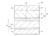
更に、メモリセル3は中間電極50を省略した構成としてもよい。この場合には、図10Aに示したメモリセル3Dのように、下部電極10側から高抵抗層32,OTS層31の順に設けられたスイッチ層30と、下部電極10側から抵抗変化層42,イオン源層41の順に設けられた記憶層40とを単純に積層させた構成としてもよい。なお、スイッチ層30とイオン源層40との積層順序は入れ替えて形成してもかまわない。また、上述した高抵抗層32における伝導パスの生成および消滅は、記憶素子3Yにおける抵抗変化層42と同様の動作であるため、高抵抗層32および抵抗変化層42を互いに共有することができる。このため、例えば図10Bに示したメモリセル3Eのように、スイッチ層30の高抵抗層32が記憶層40の抵抗変化層42を兼ねるように、高抵抗層32を間にOTS層31およびイオン源層41が配置される構成としてもよい。更に、例えば図10Cに示したメモリセル3Fのように、抵抗変化層42を2層設け(抵抗変化層42A,42B)、イオン源層41の下部電極10側および上部電極20側の両方に設け、スイッチ層30と積層して構成としてもよい。
Further, the memory cell 3 may have a configuration in which the
図11Aは、スイッチ素子3XのIV特性を表したものである。順バイアス(ここでは、書き込み電圧)を印加すると、スイッチ素子3Xは上述したように印加電圧の増加に伴って電流が上昇するが、ある閾値電圧(スイッチング閾値電圧)を超えるとオボニック閾値スイッチにより急激に電流が増大、あるいは抵抗が低くなりオン状態となる。この後、印加電圧を減少させていくと、スイッチ素子3Xの電極に流れる電流値は徐々に減少し、2回目以降の動作では、印加電圧の増加時および減少時共に近似した抵抗変化、具体的には、増加時と同等の電圧で急激に抵抗が上昇してオフ状態となる(B1)。即ち、スイッチ素子3Xの抵抗値は書き込み電圧の印加によって低抵抗状態となるが、印加電圧を閾値以下に下げると高抵抗状態に戻り、電圧印加時の抵抗値は維持されない。
FIG. 11A shows the IV characteristics of the
図11Bは、記憶素子3YのIV特性を表したものである。図11Bからわかるように、記憶素子3Yでは、印加電圧の増加に伴って電流値が上昇するが、ある閾値電圧において記憶層40の抵抗変化層42における伝導パス形成による書き込み動作が行われ、低抵抗状態へと変化する。即ち、記憶素子3Yの抵抗値は書き込み電圧の印加によって低抵抗状態となり、印加電圧停止後もその抵抗状態は維持される(B1)。
FIG. 11B shows IV characteristics of the
図11Cは、メモリセル3のIV特性を表したものである。上記記憶素子3Yとスイッチ素子3Xとを組み合わせたメモリセル3の書き込み電圧の印加開始および停止における電流値のスイッチング挙動は、記憶素子3Y(A1)およびスイッチ素子3X(B1)を合わせたものとなる(C1)。例えば、V/2バイアス方式のクロスポイントアレイの場合には、メモリセル3のC1のIV曲線上で急激に抵抗変化する閾値よりも大きな電圧を読み出し電圧(Vread)を設定し、Vread/2は抵抗変化の閾値よりも小さい電圧となるように設定する。これにより、バイアス(オン)とVread/2バイアス(オフ)との電流比で定義される選択比を大きくとることが可能となる。また、上記のように、メモリセル3のIV曲線C1はスイッチ素子3XのIV曲線B1と記憶素子3YのIV曲線の合成であるので、スイッチ素子3Xのオボニック閾値スイッチの閾値前後の抵抗変化(あるいは電流変化)が大きいほど選択比を大きくとることができる。これにより、本実施の形態におけるスイッチ素子3Xでは大きなオン/オフ比を得ることが選択比の増大となって好ましいといえる。更に、選択比が大きければ大きいほど読み出しマージンが大きくなるため、誤読み出しすることなくクロスポイントアレイサイズを大きくすることが可能となり、メモリセルアレイの更なる大容量化が可能となる。
FIG. 11C shows the IV characteristics of the memory cell 3. The switching behavior of the current value at the start and stop of application of the write voltage of the memory cell 3 in which the
これは、読み出し動作だけでなく、書き込み動作についても同様である。図11Dは、図11Cと同様にメモリセル3のIV特性を表したものである。上述したように、クロスポイントアレイでは、対象のメモリセルと同じビット線BLあるいはワード線WLに多数のビットが接続されている。このため、図11Dに示したように、Vwrite/2とIV曲線C1の点線のSet状態のIVループの交点で示される、Vwrite/2にバイアスされた
非選択時のリーク電流が大きいと非選択のメモリセルで誤書き込みを生じる虞がある。よって、書き込み動作では、記憶素子3Yを書き込む際に必要な電流が得られる電圧に書き込み電圧Vwriteを設定したうえで、Vwrite/2にバイアスされた非選択のメモリセルが誤書き込みを生じない程度のリーク電流に抑える必要がある。Vwrite/2にバイアスさ
れた非選択時のリーク電流が小さければ小さいほど大規模なクロスポイントアレイを誤書き込みなく動作させることができる。従って、書き込み動作時もスイッチ素子3Xの選択比を大きくすることが、メモリセルアレイの大容量化につながる。
This is the same for the write operation as well as the read operation. FIG. 11D shows the IV characteristics of the memory cell 3 as in FIG. 11C. As described above, in the cross point array, a large number of bits are connected to the same bit line BL or word line WL as the target memory cell. For this reason, as shown in FIG. 11D, if the leak current at the time of non-selection biased to Vwrite / 2, which is indicated by the intersection of the Vwrite / 2 and the dotted IV line of the IV curve C1, is biased to Vwrite / 2, is not selected. There is a risk of erroneous writing in the memory cells. Therefore, in the write operation, the write voltage Vwrite is set to a voltage at which a current necessary for writing to the
一方、逆バイアス(ここでは消去電圧)を印加すると、スイッチ素子3Xの消去電圧印加時における電流値の変化は、書き込み電圧を印加したサイト同様の挙動を示す(B2)。これに対して、記憶素子3Yの消去電圧印加時における電流値の変化は、消去閾値電圧以上の電圧印加によって、低抵抗状態から高抵抗状態へと変化する(A2)。図11A〜11Cに示したように、A2およびB2のIV特性を合成すると消去バイアスでのメモリセルのIV特性C2が得られる。V/2バイアス方式のクロスポイントアレイでは、通常の読み出しバイアスを書き込み側に設定するため、Vreset/2バイアスでのディスターブ電流が問題となるが、これについても、正バイアスの場合と同様に、スイッチ素子3Xのオン/オフ比、即ち選択比が大きく、オフ時のリーク電流が小さいほどクロスポイントアレイの大規模化に有利となる。
On the other hand, when a reverse bias (here, erase voltage) is applied, the change in the current value when the erase voltage is applied to the
(実験1)
まず、TiNよりなる下部電極10を逆スパッタによってクリーニングしたのち、TiN上にSiO2膜を2nmの膜厚に形成して高抵抗層32とする。次に、OTS層31と
してGeTe膜を40nmの膜厚で形成したのち、Wを30nmの膜厚で形成して上部電極20とした。続いて、フォトリソグラフィやドライエッチングなどの公知の技術を用いて素子サイズが100nmφとなるように微細加工を行い、スイッチ素子1A(サンプル1)を作製した。また、比較例として、高抵抗層32を形成していないスイッチ素子100(サンプル2)を作製した。これらサンプル1およびサンプル2の印加電圧と各電極に流れる電流値との関係を測定し、そのIV特性を図12に示した。
(Experiment 1)
First, after the
図12からわかるように、本実施の形態であるサンプル1では、サンプル2と比較して閾値電圧が増大した。また、オン/オフ比もサンプル2よりも大きくなった。即ち、スイッチ素子1Aは閾値電圧の増加と抵抗変化比の増大とが同時に実現していることがわかる。
As can be seen from FIG. 12, the threshold voltage increased in sample 1 according to the present embodiment compared to sample 2. The on / off ratio was also larger than that of sample 2 . That is, it can be seen that the switch element 1A simultaneously realizes an increase in threshold voltage and an increase in resistance change ratio.
図13A〜図13Cからわかるように、スイッチ素子1A(サンプル3,4)およびスイッチ素子100(サンプル5)は、高抵抗層32の有無によらず、ある閾値電圧を境に急激に抵抗が低下して電流が増大するオボニック閾値スイッチが見られる。図14は、図13A〜図13Cに示したサンプル3〜5の正バイアスの印加電圧増加方向のIV曲線をまとめたものである。サンプル3,4を高抵抗層32を設けていないサンプル5と比較すると、サンプル3およびサンプル4は共にオフ状態(電圧0)におけるリーク電流が低減(ほぼ0)され、さらに閾値電圧が増大している。即ち、本開示のスイッチ素子1Aは書き込み閾値電圧の高い記憶素子(例えば、記憶素子3Y)に対抗可能な良好な特性を有することがわかる。なお、サンプル3とサンプル4とを比較した場合には、SiO2を用い
たサンプル3よりもSiNを用いたサンプル4の方が、閾値電圧が高くリーク電流が小さかった。これは、SiO2およびSiNの膜厚や成膜条件によって適宜制御することがで
きる。
As can be seen from FIGS. 13A to 13C, the switch element 1A (samples 3 and 4) and the switch element 100 (sample 5) rapidly decrease in resistance at a certain threshold voltage regardless of the presence or absence of the
(実験3)
次に、サンプル3を用いて最大印加電圧を6V一定とし、スイッチ素子1Aに直列に接続されている抵抗値を変化(5kΩ,12.5kΩ,50kΩ)させることにより最大電流値を変化させた。図15は各抵抗値における正バイアスのIV曲線を示したものである。スイッチ素子1Aに流れる最大電流値が変化することにより、リーク電流と閾値電圧が変化することがわかった。次に、これらの測定から求めたサンプル3に流す最大電流とリーク電流との関係および最大電流と閾値電圧との関係を図16A,図16Bに示した。なお、リーク電流の定義は正バイアス0.5Vの電流とした。
(Experiment 3)
Next, the maximum applied voltage was kept constant at 6 V using the sample 3, and the maximum current value was changed by changing the resistance value connected in series to the switch element 1A (5 kΩ , 12.5 kΩ , 50 kΩ). . FIG. 15 shows a positive bias IV curve at each resistance value. It has been found that the leak current and the threshold voltage change as the maximum current value flowing through the switch element 1A changes. Next, FIG. 16A and FIG. 16B show the relationship between the maximum current and leakage current flowing through the sample 3 obtained from these measurements, and the relationship between the maximum current and the threshold voltage. The leak current was defined as a current with a positive bias of 0.5V.
Claims (20)
前記スイッチ層は、
カルコゲン元素を含む第1層と、
高抵抗材料を含む第2層と
を備えたスイッチ素子。 A first electrode, a second electrode disposed opposite to the first electrode, and a switch layer provided between the first electrode and the second electrode,
The switch layer is
A first layer containing a chalcogen element;
And a second layer containing a high-resistance material.
前記スイッチ素子は、
第1電極および前記第1電極に対向配置された第2電極と、前記第1電極と前記第2電極との間に設けられたスイッチ層とを有し、
前記スイッチ層は、
カルコゲン元素を含む第1層と、
高抵抗材料を含む第2層と
を備えた記憶装置。 A plurality of memory cells including a memory element and a switch element connected to the memory element,
The switch element is
A first electrode, a second electrode disposed opposite to the first electrode, and a switch layer provided between the first electrode and the second electrode,
The switch layer is
A first layer containing a chalcogen element;
And a second layer containing a high resistance material.
Priority Applications (6)
| Application Number | Priority Date | Filing Date | Title |
|---|---|---|---|
| JP2014007265A JP6151650B2 (en) | 2014-01-17 | 2014-01-17 | Storage device |
| TW103144866A TWI661535B (en) | 2014-01-17 | 2014-12-22 | Switch device and storage unit |
| US14/590,014 US9543512B2 (en) | 2014-01-17 | 2015-01-06 | Switch device and storage unit |
| KR1020150003278A KR102356740B1 (en) | 2014-01-17 | 2015-01-09 | Switch device and storage unit |
| US15/379,209 US20170098683A1 (en) | 2014-01-17 | 2016-12-14 | Switch device and storage unit |
| US15/379,390 US20170098684A1 (en) | 2014-01-17 | 2016-12-14 | Switch device and storage unit |
Applications Claiming Priority (1)
| Application Number | Priority Date | Filing Date | Title |
|---|---|---|---|
| JP2014007265A JP6151650B2 (en) | 2014-01-17 | 2014-01-17 | Storage device |
Publications (3)
| Publication Number | Publication Date |
|---|---|
| JP2015135917A JP2015135917A (en) | 2015-07-27 |
| JP2015135917A5 true JP2015135917A5 (en) | 2016-04-14 |
| JP6151650B2 JP6151650B2 (en) | 2017-06-21 |
Family
ID=53545587
Family Applications (1)
| Application Number | Title | Priority Date | Filing Date |
|---|---|---|---|
| JP2014007265A Expired - Fee Related JP6151650B2 (en) | 2014-01-17 | 2014-01-17 | Storage device |
Country Status (4)
| Country | Link |
|---|---|
| US (3) | US9543512B2 (en) |
| JP (1) | JP6151650B2 (en) |
| KR (1) | KR102356740B1 (en) |
| TW (1) | TWI661535B (en) |
Families Citing this family (32)
| Publication number | Priority date | Publication date | Assignee | Title |
|---|---|---|---|---|
| US8884261B2 (en) | 2010-08-23 | 2014-11-11 | Crossbar, Inc. | Device switching using layered device structure |
| US9685608B2 (en) | 2012-04-13 | 2017-06-20 | Crossbar, Inc. | Reduced diffusion in metal electrode for two-terminal memory |
| US10096653B2 (en) | 2012-08-14 | 2018-10-09 | Crossbar, Inc. | Monolithically integrated resistive memory using integrated-circuit foundry compatible processes |
| JP6151650B2 (en) * | 2014-01-17 | 2017-06-21 | ソニーセミコンダクタソリューションズ株式会社 | Storage device |
| US10290801B2 (en) * | 2014-02-07 | 2019-05-14 | Crossbar, Inc. | Scalable silicon based resistive memory device |
| US9716225B2 (en) | 2014-09-03 | 2017-07-25 | Micron Technology, Inc. | Memory cells including dielectric materials, memory devices including the memory cells, and methods of forming same |
| EP3262651B1 (en) * | 2015-08-07 | 2021-07-21 | Hewlett Packard Enterprise Development LP | Crossbar arrays for calculating matrix multiplication |
| CN105514136A (en) * | 2016-01-26 | 2016-04-20 | 上海新储集成电路有限公司 | Method for preparing three-dimensional resistive random access memorizer |
| JP6567441B2 (en) * | 2016-02-09 | 2019-08-28 | 株式会社東芝 | Super lattice memory and cross-point type memory device |
| US9741764B1 (en) | 2016-02-22 | 2017-08-22 | Samsung Electronics Co., Ltd. | Memory device including ovonic threshold switch adjusting threshold voltage thereof |
| KR101854023B1 (en) * | 2016-02-23 | 2018-05-02 | 연세대학교 산학협력단 | Non-linear switching device, method of fabricating the same, and non-volatile memory device having the same |
| KR102453349B1 (en) | 2016-02-25 | 2022-10-07 | 삼성전자주식회사 | Variable resistance memory devices and methods of manufacturing the same |
| KR102578481B1 (en) * | 2016-03-15 | 2023-09-14 | 삼성전자주식회사 | Semiconductor memory device and method of manufacturing the same |
| KR102495000B1 (en) * | 2016-03-18 | 2023-02-02 | 삼성전자주식회사 | Non-volatile semiconductor memory device and method of manufacturing the same |
| KR102483704B1 (en) * | 2016-03-30 | 2023-01-02 | 삼성전자주식회사 | Variable resistance memory devices and methods of manufacturing the same |
| KR101889600B1 (en) * | 2016-03-31 | 2018-08-17 | 연세대학교 산학협력단 | Non-volatile memory device and method of manufacturing the same |
| JP2017224688A (en) * | 2016-06-14 | 2017-12-21 | ソニー株式会社 | Circuit element, storage device, electronic apparatus, information writing method for circuit element, and information reading method from circuit element |
| KR102530067B1 (en) * | 2016-07-28 | 2023-05-08 | 삼성전자주식회사 | Variable resistance memory devices and methods of manufacturing the same |
| KR102584288B1 (en) | 2016-08-03 | 2023-09-27 | 삼성전자주식회사 | Non-volatile memory device |
| WO2018057012A1 (en) * | 2016-09-23 | 2018-03-29 | Intel Corporation | Threshold switching selector based memory |
| KR102389106B1 (en) * | 2016-10-04 | 2022-04-21 | 소니 세미컨덕터 솔루션즈 가부시키가이샤 | Switch elements and storage devices, and memory systems |
| US10658588B2 (en) * | 2017-04-06 | 2020-05-19 | Sony Corporation | Memory cell switch device |
| KR102366798B1 (en) | 2017-06-13 | 2022-02-25 | 삼성전자주식회사 | Semiconductor devices |
| US10861902B2 (en) | 2017-06-13 | 2020-12-08 | Samsung Electronics Co., Ltd. | Semiconductor device having magnetic tunnel junction pattern |
| US10672833B2 (en) | 2017-07-26 | 2020-06-02 | Micron Technology, Inc. | Semiconductor devices including a passive material between memory cells and conductive access lines, and related electronic devices |
| KR102465179B1 (en) | 2018-01-18 | 2022-11-08 | 에스케이하이닉스 주식회사 | Switching device, method of fabricating the same, and non-volatile memory device having the same |
| US11024372B2 (en) | 2018-08-13 | 2021-06-01 | Micron Technology, Inc. | Segregation-based memory |
| KR102630031B1 (en) * | 2018-10-05 | 2024-01-30 | 삼성전자주식회사 | Variable resistance memory device |
| KR20200041031A (en) | 2018-10-11 | 2020-04-21 | 삼성전자주식회사 | Variable resistance memory devices |
| KR102130219B1 (en) * | 2018-10-30 | 2020-07-03 | 연세대학교 산학협력단 | Non-linear switching device, method of fabricating the same, and non-volatile memory device having the same |
| JP2021103749A (en) | 2019-12-25 | 2021-07-15 | キオクシア株式会社 | Resistance change element |
| CN111584710B (en) * | 2020-04-10 | 2023-09-26 | 中国科学院上海微系统与信息技术研究所 | OTS material, gate unit and preparation method thereof |
Family Cites Families (13)
| Publication number | Priority date | Publication date | Assignee | Title |
|---|---|---|---|---|
| US6806526B2 (en) * | 2001-08-13 | 2004-10-19 | Advanced Micro Devices, Inc. | Memory device |
| US7687830B2 (en) * | 2004-09-17 | 2010-03-30 | Ovonyx, Inc. | Phase change memory with ovonic threshold switch |
| US7646630B2 (en) * | 2004-11-08 | 2010-01-12 | Ovonyx, Inc. | Programmable matrix array with chalcogenide material |
| US20080042119A1 (en) * | 2005-08-09 | 2008-02-21 | Ovonyx, Inc. | Multi-layered chalcogenide and related devices having enhanced operational characteristics |
| US7414883B2 (en) * | 2006-04-20 | 2008-08-19 | Intel Corporation | Programming a normally single phase chalcogenide material for use as a memory or FPLA |
| EP1883113B1 (en) * | 2006-07-27 | 2010-03-10 | STMicroelectronics S.r.l. | Phase change memory device |
| US20100165716A1 (en) | 2008-12-30 | 2010-07-01 | Stmicroelectronics S.R.L. | Nonvolatile memory with ovonic threshold switches |
| US7983065B2 (en) * | 2009-04-08 | 2011-07-19 | Sandisk 3D Llc | Three-dimensional array of re-programmable non-volatile memory elements having vertical bit lines |
| JP5420436B2 (en) * | 2010-01-15 | 2014-02-19 | 株式会社日立製作所 | Nonvolatile memory device and manufacturing method thereof |
| JP2012019042A (en) * | 2010-07-07 | 2012-01-26 | Sony Corp | Memory element and memory device |
| US9287498B2 (en) * | 2011-09-14 | 2016-03-15 | Intel Corporation | Dielectric thin film on electrodes for resistance change memory devices |
| JP6151650B2 (en) * | 2014-01-17 | 2017-06-21 | ソニーセミコンダクタソリューションズ株式会社 | Storage device |
| US9716225B2 (en) * | 2014-09-03 | 2017-07-25 | Micron Technology, Inc. | Memory cells including dielectric materials, memory devices including the memory cells, and methods of forming same |
-
2014
- 2014-01-17 JP JP2014007265A patent/JP6151650B2/en not_active Expired - Fee Related
- 2014-12-22 TW TW103144866A patent/TWI661535B/en not_active IP Right Cessation
-
2015
- 2015-01-06 US US14/590,014 patent/US9543512B2/en active Active
- 2015-01-09 KR KR1020150003278A patent/KR102356740B1/en active IP Right Grant
-
2016
- 2016-12-14 US US15/379,209 patent/US20170098683A1/en not_active Abandoned
- 2016-12-14 US US15/379,390 patent/US20170098684A1/en not_active Abandoned
Similar Documents
| Publication | Publication Date | Title |
|---|---|---|
| JP2015135917A5 (en) | ||
| JP6151650B2 (en) | Storage device | |
| JP6772124B2 (en) | Switch element and storage device | |
| US11183633B2 (en) | Switch device, storage apparatus, and memory system | |
| US9136468B2 (en) | Nonvolatile semiconductor memory device | |
| JP4538067B2 (en) | Semiconductor memory device | |
| WO2016158430A1 (en) | Switch element and storage device | |
| US7869259B2 (en) | Resistance change memory, and data write and erase methods thereof | |
| JP4529654B2 (en) | Storage element and storage device | |
| JP2009135206A (en) | Memory cell | |
| JP5598338B2 (en) | Storage device and operation method thereof | |
| JP2009141225A (en) | Variable resistive element, method for manufacturing variable resistive element, nonvolatile semiconductor storage device | |
| JP2012204404A (en) | Resistance change nonvolatile semiconductor memory device | |
| JP2012023271A (en) | Semiconductor memory | |
| JP6787785B2 (en) | Switch element and storage device | |
| KR102507303B1 (en) | Memory device | |
| US9112132B2 (en) | Resistance-variable memory device | |
| WO2017217119A1 (en) | Circuit element, storage device, electronic device, method for writing information to circuit element, and method for reading information from circuit element | |
| JP2020047316A (en) | Non-volatile storage device | |
| JPWO2018190071A1 (en) | Storage device | |
| JP2015170853A (en) | Semiconductor storage device | |
| JP2011044443A (en) | Nonvolatile memory element and process for producing the same, and nonvolatile semiconductor device using the nonvolatile memory element | |
| JP2010278275A (en) | Semiconductor memory device | |
| JP6602328B2 (en) | Semiconductor memory device | |
| Yu | RRAM Array Architecture |