JP2014532862A - Test equipment with configurable interface - Google Patents
Test equipment with configurable interface Download PDFInfo
- Publication number
- JP2014532862A JP2014532862A JP2014538796A JP2014538796A JP2014532862A JP 2014532862 A JP2014532862 A JP 2014532862A JP 2014538796 A JP2014538796 A JP 2014538796A JP 2014538796 A JP2014538796 A JP 2014538796A JP 2014532862 A JP2014532862 A JP 2014532862A
- Authority
- JP
- Japan
- Prior art keywords
- test
- port
- test equipment
- uut
- fpga
- Prior art date
- Legal status (The legal status is an assumption and is not a legal conclusion. Google has not performed a legal analysis and makes no representation as to the accuracy of the status listed.)
- Pending
Links
Images


Classifications
-
- G—PHYSICS
- G01—MEASURING; TESTING
- G01R—MEASURING ELECTRIC VARIABLES; MEASURING MAGNETIC VARIABLES
- G01R31/00—Arrangements for testing electric properties; Arrangements for locating electric faults; Arrangements for electrical testing characterised by what is being tested not provided for elsewhere
- G01R31/28—Testing of electronic circuits, e.g. by signal tracer
- G01R31/317—Testing of digital circuits
- G01R31/3181—Functional testing
- G01R31/319—Tester hardware, i.e. output processing circuits
- G01R31/31903—Tester hardware, i.e. output processing circuits tester configuration
- G01R31/31908—Tester set-up, e.g. configuring the tester to the device under test [DUT], down loading test patterns
-
- G—PHYSICS
- G01—MEASURING; TESTING
- G01R—MEASURING ELECTRIC VARIABLES; MEASURING MAGNETIC VARIABLES
- G01R31/00—Arrangements for testing electric properties; Arrangements for locating electric faults; Arrangements for electrical testing characterised by what is being tested not provided for elsewhere
- G01R31/28—Testing of electronic circuits, e.g. by signal tracer
- G01R31/2851—Testing of integrated circuits [IC]
- G01R31/2886—Features relating to contacting the IC under test, e.g. probe heads; chucks
- G01R31/2889—Interfaces, e.g. between probe and tester
-
- G—PHYSICS
- G01—MEASURING; TESTING
- G01R—MEASURING ELECTRIC VARIABLES; MEASURING MAGNETIC VARIABLES
- G01R31/00—Arrangements for testing electric properties; Arrangements for locating electric faults; Arrangements for electrical testing characterised by what is being tested not provided for elsewhere
- G01R31/28—Testing of electronic circuits, e.g. by signal tracer
- G01R31/317—Testing of digital circuits
- G01R31/31704—Design for test; Design verification
-
- G—PHYSICS
- G01—MEASURING; TESTING
- G01R—MEASURING ELECTRIC VARIABLES; MEASURING MAGNETIC VARIABLES
- G01R31/00—Arrangements for testing electric properties; Arrangements for locating electric faults; Arrangements for electrical testing characterised by what is being tested not provided for elsewhere
- G01R31/28—Testing of electronic circuits, e.g. by signal tracer
- G01R31/317—Testing of digital circuits
- G01R31/3181—Functional testing
- G01R31/319—Tester hardware, i.e. output processing circuits
- G01R31/31917—Stimuli generation or application of test patterns to the device under test [DUT]
- G01R31/31926—Routing signals to or from the device under test [DUT], e.g. switch matrix, pin multiplexing
Abstract
概して、試験機器は、制御システムとの通信を含む、試験機器の動作を制御するようにプログラムされ、かつ試験機器にインターフェース接続されたデバイスを試験するために、1つ以上の試験プログラムを実行するようにプログラムされた処理システムを含み、処理システムが、複数の処理デバイスと、試験機器にインターフェース接続されたデバイスと通信を交換する、構成可能なインターフェースとを含み、構成可能なインターフェースが、異なる構成が割り当て可能である、物理ポートを含む。In general, a test instrument executes one or more test programs to test devices that are programmed and interfaced to the test instrument, including communication with a control system. A processing system programmed in such a manner that the processing system includes a plurality of processing devices and a configurable interface that exchanges communications with devices interfaced to the test equipment, the configurable interfaces being different configurations Includes physical ports that can be assigned.
Description
本開示は、概して、構成可能なインターフェースを有する試験機器に関する。 The present disclosure relates generally to test equipment having a configurable interface.
自動試験装置(ATE)は、半導体デバイス及び回路基板アセンブリ等、電子部品の製造において役割を果たす。製造業者は概して、製造プロセスの間にデバイスの動作を検証するために、自動試験装置、又は「テスタ機器」を使用する。このようなデバイスは、「被試験デバイス」(DUT)又は「被試験ユニット」(UUT)と称される。障害の早期検出は、早期検出されない場合に不良デバイスを処理することによって生じるコストを排除し、それによって、製造コスト全体を削減する。製造業者はまた、多様な仕様を評価するためにもATEを使用する。デバイスは、速度等、分野の異なるレベルの性能に従って、試験し、分類することができる。デバイスは、その実性能レベルに従って、ラベル付けし、販売することができる。 Automatic test equipment (ATE) plays a role in the manufacture of electronic components such as semiconductor devices and circuit board assemblies. Manufacturers typically use automatic test equipment, or “tester equipment”, to verify device operation during the manufacturing process. Such a device is referred to as a “device under test” (DUT) or a “unit under test” (UUT). Early detection of faults eliminates the costs caused by processing bad devices if they are not detected early, thereby reducing overall manufacturing costs. Manufacturers also use ATE to evaluate various specifications. Devices can be tested and classified according to different levels of performance, such as speed. Devices can be labeled and sold according to their actual performance level.
概して、一態様において、試験機器は、制御システムとの通信を含む、試験機器の動作を制御するようにプログラムされ、かつ試験機器にインターフェース接続されたデバイスを試験するために、1つ以上の試験プログラムを実行するようにプログラムされた処理システムを含み、処理システムが、複数の処理デバイスと、試験機器にインターフェース接続されたデバイスと通信を交換する、構成可能なインターフェースと、を含み、構成可能なインターフェースが、異なる構成が割り当て可能である、物理ポートを含む。 In general, in one aspect, a test instrument is programmed to control the operation of the test instrument, including communication with a control system, and one or more tests to test a device interfaced to the test instrument. A processing system programmed to execute the program, the processing system including and configurable to a plurality of processing devices and a configurable interface that exchanges communications with devices interfaced to the test equipment The interface includes physical ports to which different configurations can be assigned.
概して、別の態様において、方法は、制御システムとの通信を含む、試験機器の動作を制御するように処理システムを構成することを含み、構成することが、試験機器にインターフェース接続されたデバイスを試験するために、1つ以上の試験プログラムを実行するように処理システムをプログラムすることを含み、処理システムが、複数の処理デバイスを含む。方法は、試験機器にインターフェース接続されたデバイスと通信を交換する、構成可能なインターフェースを提供することを更に含み、構成可能なインターフェースが、異なる構成が割り当て可能である、物理ポートを含む。 In general, in another aspect, a method includes configuring a processing system to control operation of a test instrument, including communication with a control system, wherein configuring configures a device interfaced to the test instrument. To test, the processing system includes programming the processing system to execute one or more test programs, the processing system including a plurality of processing devices. The method further includes providing a configurable interface that exchanges communications with a device interfaced to the test equipment, the configurable interface including a physical port to which a different configuration can be assigned.
態様には以下の特徴の1つ以上が含まれてもよい。構成可能なインターフェースは、プログラム可能な論理を含み、論理が、論理へのロードのアプリケーションを通じてプログラム可能であり、ロードが、物理ポートが異なる構成を想定することを可能にする機能性を提供する。プログラム可能な論理は、フィールドプログラマブルゲートアレイ(FPGA)を含み、ロードは、物理ポートが、制御入力に応答して異なる構成を想定することを可能にする単一のロードである。単一のロードは更に、FPGAが試験機器にインターフェース接続されたデバイス上で1つ以上の試験を実施するように構成する。異なる構成は、少なくとも部分的に、複数の処理デバイスのうちのどれが試験機器にインターフェース接続されたデバイスと通信するかに基づいて、物理ポートに割り当て可能である。処理システムは、制御入力をFPGAに提供するようにプログラムされる。異なる構成は、ポートが入力又は出力として動作するかどうかを含む、ポートの機能に関係する。異なる構成は、ポートの幅に関係する。異なる構成は、ポートを通じて伝送される信号の周波数に関係する。異なる構成は、ポートと関連付けられるメモリの深さに関係する。処理システムは、試験機器にインターフェース接続されたデバイスを試験するために、1つ以上の試験プログラムを実行するようにプログラム可能であり、かつ試験機器の動作を制御するようにプログラム可能である、第1の処理サブシステムと、デバイス試験専用である第2の処理サブシステムとを含み、第2の処理システムが、デバイスを試験するために、1つ以上の試験プログラムを実行するようにプログラム可能である、複数の処理デバイスを含む。 Aspects may include one or more of the following features. The configurable interface includes programmable logic, where the logic is programmable through the application of load to logic, and the load provides functionality that allows the physical ports to assume different configurations. Programmable logic includes a field programmable gate array (FPGA), and a load is a single load that allows a physical port to assume different configurations in response to control inputs. The single load is further configured so that the FPGA performs one or more tests on the device interfaced to the test equipment. Different configurations can be assigned to physical ports based at least in part on which of the plurality of processing devices communicates with the device interfaced to the test equipment. The processing system is programmed to provide control inputs to the FPGA. Different configurations relate to the function of the port, including whether the port operates as an input or output. The different configurations relate to the port width. Different configurations relate to the frequency of the signal transmitted through the port. Different configurations relate to the depth of memory associated with the port. The processing system is programmable to execute one or more test programs to test a device interfaced to the test equipment and is programmable to control the operation of the test equipment. One processing subsystem and a second processing subsystem dedicated to device testing, wherein the second processing system is programmable to execute one or more test programs to test the device. A plurality of processing devices are included.
この概要の項を含む、本開示で説明される特徴のうちの、2つ以上を組み合わせることにより、本明細書では具体的に説明されない実施形態を形成することができる。 Combining two or more of the features described in this disclosure, including this summary section, can form embodiments not specifically described herein.
本明細書において説明されるシステム及び技法、又はその部分は、1つ以上の非一時的機械可読記憶媒体上に記憶され、かつ1つ以上の処理デバイス上で実行可能である命令を含む、コンピュータプログラム製品として実装されてもよい。本明細書において説明されるシステム及び技法、又はその部分は、記載の機能を実装するために実行可能な命令を記憶するように、1つ以上の処理デバイス及びメモリを含むことができる装置、方法、又は電子システムとして実装されてもよい。 The systems and techniques described herein, or portions thereof, include instructions that are stored on one or more non-transitory machine-readable storage media and that are executable on one or more processing devices. It may be implemented as a program product. The systems and techniques described herein, or portions thereof, can include one or more processing devices and memory to store instructions that are executable to implement the described functionality. Or as an electronic system.
1つ以上の実装の詳細を、添付の図面及び以下の説明で明らかにする。他の特徴、目的及び利点は、発明を実施するための形態及び図面、並びに特許請求の範囲から明白となるであろう。 The details of one or more implementations are set forth in the accompanying drawings and the description below. Other features, objects, and advantages will be apparent from the description and drawings, and from the claims.
本明細書において、構成可能であるインターフェースを含む試験機器を説明する。試験機器は、複数の処理デバイスを含むことができる、処理システムを含む。処理システムは、試験機器の動作を制御するようにプログラムされる。処理システムはまた、試験機器にインターフェース接続されたデバイスを試験するために、1つ以上の試験プログラムを実行するようにもプログラムされる。試験機器は、試験機器にインターフェース接続されたデバイス(例えば、被試験ユニット、又は「UUT」)と通信が交換される、構成可能なインターフェースを含む。この例示的な実装において、構成可能なインターフェースは、異なる構成が割り当て可能である、物理ポートを含む。この例示的な実装において、インターフェースは、複数の選択可能なインターフェース構成を含む、単一のプログラムイメージを使用して、リアルタイムで構成可能である。 Described herein are test instruments that include configurable interfaces. The test equipment includes a processing system that can include a plurality of processing devices. The processing system is programmed to control the operation of the test equipment. The processing system is also programmed to execute one or more test programs to test devices interfaced to the test equipment. The test equipment includes a configurable interface in which communication is exchanged with a device (eg, a unit under test, or “UUT”) interfaced to the test equipment. In this exemplary implementation, the configurable interface includes physical ports to which different configurations can be assigned. In this exemplary implementation, the interface can be configured in real time using a single program image that includes multiple selectable interface configurations.
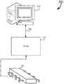
図1は、前述の試験機器100の例示的な実装のブロック図である。図1において、試験機器100は、3階層の処理システムを含む。しかしながら、他の例示的な実装において、これより多い、又は少ない階層が存在してもよい。試験機器100の異なる階層は、UUTに対するその階層の相対的関係を反映する。本実施例において、第1の階層101は、コンピュータ102を含む。本実施例において、コンピュータ102は、外部ネットワークとの通信等、試験機器100の多様な機能を制御するシステム処理デバイスを含む。加えて、コンピュータ102は、以下に説明されるように、多様な試験動作を実施するようにプログラム可能である。第2の階層104は、試験専用である、1つ以上の処理デバイス106〜108を含む。例えば、処理デバイス106〜108は、典型的に、試験機器の制御及びネットワーク通信のような、試験以外の機能を実施しない。しかしながら、いくつかの実施例において、処理デバイス106〜108は、通信、及び制御の流れ、中断、タイミング等、いくつかのハウスキーピング機能を実施してもよい。第3の階層110は、UUT 115に対するインターフェースとして機能するように、かつUUT上で1つ以上の試験動作を実施するようにプログラム可能である、論理111〜113を含む。
FIG. 1 is a block diagram of an exemplary implementation of the
この例示的な第1の階層101において、コンピュータ102は、1つ以上のマイクロプロセッサ又は単一のマルチコアマイクロプロセッサ(図示せず)等、1つ以上の処理デバイスを含む。コンピュータ102はまた、外部環境との試験機器の通信を制御するため、かつ試験機器100の動作を制御するための多様な「ハウスキーピング」機能を実施するための実行可能なコードを記憶するメモリ(図示せず)も含む。例えば、コンピュータ102は、ネットワークインターフェース120上で試験機器と1つ以上の外部エンティティとの間の通信を交換すること、マルウェアに対して試験機器をスキャンすること、メモリ管理、出力制御、及びUUTの試験に特に関係しない他の機能を担ってもよい。
In this exemplary
コンピュータ102はまた、試験機器100にインターフェース接続されたUUT(例えば、115)上で試験動作を実施するようにもプログラム可能である。試験動作は、バス速度、反応時間、又はUUTの任意の他の適切な動作態様を試験することを含むことができるが、これらに限定されない。一般に、実施される試験は、試験されるデバイスの種類、及び試験中に求められる情報に依存する。
Computer 102 is also programmable to perform test operations on a UUT (eg, 115) interfaced to test
1つ以上の試験プログラムが、コンピュータ102上のメモリにロードされ、試験を実施するために、コンピュータ102内の処理デバイス(複数を含む)によって実行されてもよい。試験を実施している間、コンピュータ102は、試験機器100の動作状態を保つために、上で説明されるもののような他の機能を実施し続けてもよい。このため、試験レイテンシ(例えば、試験の開始と試験結果の受信との間の時間量)は、ミリ秒単位であり得る。これは、試験レイテンシの例に過ぎない。異なるシステムにおいて、コンピュータ102内の処理デバイス(複数を含む)の速度、コンピュータ102内で試験プログラムを実行するために利用可能なメモリの量等、多数の因子が試験レイテンシに影響を与える場合がある。
One or more test programs may be loaded into memory on the computer 102 and executed by processing device (s) in the computer 102 to perform the test. While performing the test, the computer 102 may continue to perform other functions, such as those described above, to keep the
コンピュータ102を介して試験を実施することの可能な利点は、試験プログラムの開発コストに関係する。より具体的には、コンピュータ102は、MICROSOFT(登録商標)WINDOWS(登録商標)又は任意の他の比較的操作が簡単なオペレーティングシステム等、オペレーティングシステム(OS)を実行することができる。オペレーティングシステム等の試験プログラムの開発に利用できるツールは、典型的に広く入手可能で、一般に、試験プログラム開発者によく知られている。この結果、コンピュータ102上で実行するために、コンピュータ102上で試験プログラムを開発するコストは、多階層アーキテクチャの他の階層上で実行するために試験プログラムを開発するコストよりも少なくすることができる。しかしながら、この一般化は、全ての事例では該当しない場合がある。 A possible advantage of conducting a test via computer 102 is related to the cost of developing the test program. More specifically, the computer 102 can execute an operating system (OS), such as MICROSOFT (R) WINDOWS (R) or any other relatively easy operating system. Tools that can be used to develop test programs such as operating systems are typically widely available and are generally well known to test program developers. As a result, the cost of developing a test program on computer 102 for execution on computer 102 can be less than the cost of developing a test program for execution on other tiers of a multi-tier architecture. . However, this generalization may not apply in all cases.
本実施例において、第2の階層104は、複数の埋め込み処理デバイス106〜108を含む。ここでは、3つの埋め込み処理デバイスが示されるが、しかしながら、試験機器100は、例えば、1つ、2つ、4つ、5つ以上等、任意の適切な数の埋め込み処理デバイスを含んでもよい。これらの処理デバイスは、これらが、試験機器100に組み込まれ、かつ、試験機能の実施専用(例えば、試験機器100にインターフェース接続されたUUTを試験するために)であるという意味で埋め込みである。埋め込み処理デバイス106〜108は、典型的に、コンピュータ102によって実施される、上で説明される「ハウスキーピング」動作等の試験機器動作を担わない。しかしながら、いくつかの実装において、埋め込み処理デバイス106〜108は、1つ以上のそのような動作、又はUUT試験に特に関係しない、他の動作を実施するようにプログラムされてもよい。
In the present embodiment, the
各埋め込み処理デバイス106〜108は、例えば、単一のコア又は複数のコアを有するマイクロコントローラ又はマイクロプロセッサ等を含むことができる。各マイクロプロセッサは、直接又はコンピュータ102を介して、プログラム可能である。例えば、試験機器100のユーザーは、埋め込み処理デバイス106をプログラムするために、コンピュータ102のオペレーティングシステムと相互作用することができる。あるいは、各埋め込み処理デバイスがプログラムされる場合がある、例えば、ハードウェア又はソフトウェア等、直接のインターフェースが存在してもよい。プログラミングは、この文脈において、それぞれの埋め込み処理デバイス上へ1つ以上の試験プログラムを記憶することを指し、試験プログラムは、UUTを試験するために、その埋め込み処理デバイス上で実行することができる。
Each embedded processing device 106-108 may include, for example, a microcontroller or microprocessor having a single core or multiple cores. Each microprocessor is programmable directly or via computer 102. For example, a user of the
図1に示されるように、各埋め込み処理デバイスは、コンピュータ102、及びそれぞれのプログラム可能な論理(本実施例において、フィールドプログラマブルゲートアレイ(FPGA))にインターフェース接続される。以下に説明するように、各FPGAは、試験対象の別個のUUT(図示せず)、又は単一のUUTの一部(例えば、示されるようにそのUUT上のバス122、123、124)に対するインターフェースとして機能する。したがって、本実施例において、各埋め込み処理デバイスは、試験されている、対応するUUT、又はその一部の専用に設計された試験プログラムでプログラムされてもよい。記載されるように、適切な試験プログラムは、埋め込み処理デバイスに直接ロードされてもよく、又はコンピュータ102を介してロードされてもよい。各埋め込み処理デバイスは、その独自の試験プログラムを別個に、及び他の埋め込み処理デバイスと同時に実行してもよい。いくつかの実装において、それらのそれぞれの試験プログラムがどのように実行されるかについて、埋め込み処理デバイス間で協調が存在してもよい。そのような協調は、埋め込み処理デバイス自体によって、又はコンピュータ102によって実装されてもよい。いくつかの実装において、協調には、アーキテクチャの異なる階層にあるデバイスが関与してもよい。いくつかの実装において、異なる埋め込み処理デバイス106〜108は、適切な協調を用いて、又は用いずに、同じ試験プログラムの異なる部分(例えば、モジュール)を実装してもよい。
As shown in FIG. 1, each embedded processing device is interfaced to a computer 102 and respective programmable logic (in this example, a field programmable gate array (FPGA)). As described below, each FPGA is for a separate UUT (not shown) to be tested, or a portion of a single UUT (eg,
埋め込み処理デバイスを介して試験を実施することの可能な利点は、試験レイテンシに関係する。より具体的には、埋め込み処理デバイスは、主に試験専用であるため、それらのリソースは典型的に、他のタスクによる負担がかからない。この結果、試験レイテンシは、コンピュータ102によって達成するよりも少なくすることができる。例えば、埋め込み処理デバイスの試験レイテンシは、マイクロ秒の単位であり得る。しかしながら、これは、埋め込み処理デバイスの試験レイテンシの例に過ぎない。異なるシステムにおいて、処理デバイスの速度、試験プログラムを実行するために利用可能なメモリの量等、多数の因子が試験レイテンシに影響を与える場合がある。したがって、前述の一般化は、全ての事例では該当しない場合がある。 A possible advantage of performing a test via an embedded processing device relates to test latency. More specifically, because embedded processing devices are primarily dedicated to testing, their resources are typically not burdened by other tasks. As a result, the test latency can be less than achieved by the computer 102. For example, the test latency of an embedded processing device can be in units of microseconds. However, this is only an example of embedded processing device test latency. In different systems, a number of factors can affect test latency, such as the speed of the processing device and the amount of memory available to execute the test program. Therefore, the generalization described above may not apply in all cases.
更に、埋め込み処理デバイス上で試験プログラムを開発するためのツールが利用可能である。この結果、埋め込み処理デバイス上で実行するために、埋め込み処理デバイス上で試験プログラムを開発するコストは、FPGA等、ハードウェア上で実行するために、試験プログラムを開発するコストより少なくすることができる。 In addition, tools are available for developing test programs on embedded processing devices. As a result, the cost of developing a test program on the embedded processing device for execution on the embedded processing device can be less than the cost of developing the test program for execution on hardware such as an FPGA. .
第3の階層110は、例えば、FPGA 111〜113等、プログラム可能な論理を含むが、FPGAの代わりに、他の種類のプログラム可能な論理が使用されてもよい。各FPGAは、FPGAにプログラムイメージをロードすることによって構成される。このプログラムイメージは、「FPGAロード」と称される。本実施例において、各FPGAは、UUT又はその一部(例えば、UUTバス)と試験機器100との間のインターフェースとして機能するように構成される。例えば、FPGAは、ポート幅、ポート速度、入力ポートの数、出力ポートの数等を指定することができる。
The
第1の階層101のコンピューティングデバイス(複数を含む)(例えば、コンピュータ102)及び第2の階層104のコンピューティングデバイス(複数を含む)(例えば、埋め込み処理デバイス106〜108)は、第3の階層110を通じて、UUT 115にアクセスする。例えば、図1に示されるように、各埋め込み処理デバイスは、対応するFPGAを通じて、UUT 115と通信することができる。コンピュータ102は、どのUUT、又はUUTのどの部分が、現在試験されているかに依存して、1つ以上のFPGAを通じて、UUT 115と通信してもよい。いくつかの実装において、FPGAによって実装される各インターフェースは、プログラム可能である。他の実装において、各FPGAによって実装されるインターフェースは、静的である(例えば、プログラム可能ではない)。
The
各FPGAはまた、FPGAがインターフェース接続される、対応するUUT、又はその一部上で1つ以上の試験を実施するように構成されてもよい。例えば、各FPGAに対するFPGAのロードは、UUTの多様な態様を試験するために、FPGAによって実行される、1つ以上の試験ルーチンを含むことができる。上記のように、実装されるルーチンは、試験されているデバイス、及び試験中に求められる情報に依存する。各FPGAによって実行される試験ルーチンは、他のFPGAによって実行される他の試験ルーチンとは独立して実行されてもよく、又は、多様なFPGAの間で協調が存在してもよい。各FPGAは、それ独自の試験ルーチンを別個に、及び他の埋め込み処理デバイスと同時に実行することができる。いくつかの実装において、それらのそれぞれの試験プログラムがどのように実行されるかについて、FPGA間で協調が存在してもよい。このような協調は、FPGA自体によって、それらの対応する埋め込み処理デバイスによって、又はコンピュータ102によって実装されてもよい。いくつかの実装において、協調には、アーキテクチャの異なる階層にあるデバイスが関与してもよい。例えば、コンピュータ102は、埋め込み処理デバイス106〜108と連携して、それぞれのFPGA 111〜113の動作を協調させることができる。いくつかの実装において、異なるFPGAは、適切な協調を用いて、又は用いずに、同じ試験ルーチンの異なる部分(例えば、モジュール)を実装してもよい。 Each FPGA may also be configured to perform one or more tests on the corresponding UUT, or a portion thereof, to which the FPGA is interfaced. For example, the FPGA load for each FPGA may include one or more test routines executed by the FPGA to test various aspects of the UUT. As described above, the routines implemented depend on the device being tested and the information required during the test. The test routines executed by each FPGA may be executed independently of other test routines executed by other FPGAs, or there may be coordination among various FPGAs. Each FPGA can run its own test routines separately and concurrently with other embedded processing devices. In some implementations, there may be cooperation between the FPGAs as to how their respective test programs are executed. Such coordination may be implemented by the FPGA itself, by their corresponding embedded processing device, or by the computer 102. In some implementations, collaboration may involve devices at different levels of the architecture. For example, the computer 102 can coordinate the operations of the FPGAs 111 to 113 in cooperation with the embedded processing devices 106 to 108. In some implementations, different FPGAs may implement different parts (eg, modules) of the same test routine with or without proper coordination.
FPGAを介して試験を実施することの可能な利点は、試験レイテンシに関係する。より具体的には、FPGAは、ハードウェアデバイスであるため、埋め込み処理デバイス106〜108又はコンピュータ102内のいずれかにプログラムされる試験ルーチンよりも高速で実行することが可能である。この結果、試験レイテンシは、埋め込み処理デバイス106〜108又はコンピュータ102によって達成されるよりも少なくすることができる。例えば、プログラム可能なデバイスの試験レイテンシは、ナノ秒の単位であり得る。しかしながら、これは、FPGAの試験レイテンシの例に過ぎない。異なるシステムにおいて、多数の因子が試験レイテンシに影響を与える場合がある。したがって、前述の一般化は、全ての事例では該当しない場合がある。 A possible advantage of performing the test via the FPGA relates to test latency. More specifically, because the FPGA is a hardware device, it can run faster than a test routine programmed into either the embedded processing device 106-108 or the computer 102. As a result, the test latency can be less than that achieved by the embedded processing devices 106-108 or the computer 102. For example, the test latency of a programmable device can be in nanoseconds. However, this is only an example of FPGA test latency. In different systems, a number of factors can affect test latency. Therefore, the generalization described above may not apply in all cases.
いくつかの実装において、試験は、アーキテクチャの1つの階層又は別の階層によって、排他的に実施されてもよい。例えば、コンピュータ102は、UUTを試験するために、1つ以上の試験プログラムを実行するようにプログラムされてもよく、一方、アーキテクチャの他の階層上のデバイスは、UUT試験を実施しない。埋め込み処理デバイス106〜108は、UUTを試験するために、1つ以上の試験プログラムを実行するようにプログラムされてもよく、一方、アーキテクチャの他の階層上のデバイスは、UUT試験を実施しない。FPGA 111〜113は、デバイス上で1つ以上の試験を実行するように構成されてもよく、一方、アーキテクチャの他の階層上のデバイスは、UUT試験を実施しない。試験を実施していないデバイスは、この時間中、必ずしも休眠状態ではない。例えば、コンピュータ102は、上で説明されるハウスキーピング動作を実施し続けてもよく、FPGAは、UUTへ/UUTからデータをルーティングし続けてもよく(すなわち、UUTに対するインターフェースとして機能する)、埋め込み処理デバイスは、協調又は他の通信(例えば、FPGAからコンピュータ102へ試験結果を伝送すること)で作動状態であり続けてもよい。 In some implementations, testing may be performed exclusively by one or another layer of architecture. For example, the computer 102 may be programmed to run one or more test programs to test the UUT, while devices on other layers of the architecture do not perform UUT testing. Embedded processing devices 106-108 may be programmed to run one or more test programs to test the UUT, while devices on other layers of the architecture do not perform UUT testing. FPGAs 111-113 may be configured to perform one or more tests on the device, while devices on other layers of the architecture do not perform UUT testing. Devices that have not been tested are not necessarily dormant during this time. For example, the computer 102 may continue to perform the housekeeping operations described above, and the FPGA may continue to route data to / from the UUT (ie, function as an interface to the UUT) and embedded The processing device may continue to operate in a coordinated or other communication (eg, transmitting test results from the FPGA to the computer 102).
他の実装において、試験は、アーキテクチャの異なる階層によって、同時又は連携して実施されてもよい。例えば、コンピュータ102、埋め込み処理デバイス106〜108、及びFPGA 111〜113のうちの2つ以上は、単一のUUT又は複数のUUT上で1つ以上の試験動作を実施するために、同時に又は同じ試験順序内で、協調して機能することができる。このような協調を有効にするために、適切なプログラミングが、コンピュータ102及び/若しくは埋め込み処理デバイス106〜108内にロードされ、並びに/又は適切なイメージがFPGA内にロードされる。例として、第1の試験は、コンピュータ102によってUUT上で実施されてもよく、第2の試験は、埋め込み処理デバイス106によってUUT上で実施されてもよく、第3の試験は、FPGA 111によってUUT上で実施されてもよい。第1、第2、及び第3の試験は、別個の試験、又は同じ試験順序の一部であってもよい。第1、第2、及び第3の試験からのデータは、適切な試験結果を取得するために、例えば、コンピュータ102内で組み合わされ、処理されてもよい。これらの試験結果は、分析及び報告のために、外部のコンピュータ(図示せず)へ送信されてもよい。アーキテクチャの階層のいずれか又は別の(例えば、第三者)当事者のコンピュータ(図示せず)が、協調を実施してもよい。 In other implementations, testing may be performed simultaneously or in concert by different layers of the architecture. For example, two or more of the computer 102, embedded processing devices 106-108, and FPGAs 111-113 may be simultaneously or the same to perform one or more test operations on a single UUT or multiple UUTs. Can work in concert within a test sequence. To enable such collaboration, appropriate programming is loaded into computer 102 and / or embedded processing devices 106-108, and / or appropriate images are loaded into the FPGA. As an example, the first test may be performed on the UUT by the computer 102, the second test may be performed on the UUT by the embedded processing device 106, and the third test may be performed by the FPGA 111. It may be implemented on the UUT. The first, second, and third tests may be separate tests or part of the same test sequence. Data from the first, second, and third tests may be combined and processed, for example, within the computer 102 to obtain appropriate test results. These test results may be sent to an external computer (not shown) for analysis and reporting. Any of the architectural hierarchies or another (eg, a third party) party computer (not shown) may implement the collaboration.
アーキテクチャの1つ以上の階層がプログラムされていない実装において、プログラムされていない階層は迂回されてもよい(少なくとも、それらの試験機能が関与する限り)。プログラムされていない階層は、プログラミング並びに階層間及び外部のネットワークとの通信に関係する上で説明されるもののような多様な機能を実施するように、事前プログラム、又は事前構成されてもよい。 In implementations in which one or more layers of the architecture are not programmed, the unprogrammed layers may be bypassed (at least as long as their test functions are involved). Unprogrammed hierarchies may be pre-programmed or pre-configured to perform various functions such as those described above relating to programming and communication between hierarchies and external networks.
多様な階層にあるデバイスは、リアルタイムでプログラム又は構成されてもよい。この文脈において、「リアルタイム」は、試験時点で、又は試験時間直前にプログラムすることを含む。すなわち、試験機器は、UUT上で実行される試験プログラムで事前プログラムされている必要はない。それらの試験プログラムは、適切なタイミングで、機器内に組み込まれてもよい。試験機器上の既存の試験プログラムは、同様に、必要に応じて、新しい試験プログラムと置換されてもよい。 Devices in various layers may be programmed or configured in real time. In this context, “real time” includes programming at the time of the test or just before the test time. That is, the test equipment need not be pre-programmed with a test program executed on the UUT. Those test programs may be incorporated into the device at an appropriate timing. Existing test programs on the test equipment may likewise be replaced with new test programs as needed.
図2は、プログラム可能な論理201の実施例を示し、これは、試験機器100の一部であってもよい。プログラム可能な論理201は、例えば、上で説明されるようなFPGA、又は任意の他の適切な種類のプログラム可能な論理であってもよい。この文脈において、プログラム可能な論理は、UUTに対するインターフェース208を含む。インターフェース208は、接続されたUUTとデータを交換する際に使用される構成要素(例えば、ポート、メモリ等)を含む。インターフェースは、以下で説明されるように、インターフェースの異なる要素に、記憶された構成情報に基づいて、異なる役割が割り当てられてもよいという意味で構成可能である。有利に、インターフェースは、異なる試験が、例えば、異なるルーチンを使用する、又は異なるデバイスによって、UUT上で実施されるように構成され得るという意味で、リアルタイムで構成可能であってもよい。
FIG. 2 shows an example of
本実施例において、プログラム可能な論理201は、複数の試験チャネルを含む。各試験チャネルは、物理ポート202a〜202nに対応する。各物理ポートは、プログラム可能な論理上の、ピン又はスロット等、インターフェース要素に対応してもよい。これらの物理ポートは、UUTの係合するコネクタにインターフェース接続するように構造化される。本実施例において、プログラム可能な論理201は、128の物理ポートを含むが、しかしながら、他の実施例において、異なる数の物理ポートが使用されてもよい。
In this example,
メモリ204(例えば、ランダムアクセスメモリ「RAM」)は、物理ポートの各々と関連付けられてもよい。このメモリは、示されるように、同じ隣接するメモリ空間の部分であってもよく、又は異なるメモリ空間の一部であってもよい。試験データは、メモリ204から、物理ポートを通じて、UUTへ転送されてもよい。試験結果データは、UUTから、物理ポートを通じて、メモリ204へ転送されてもよい。図1に関して上で説明されるように、試験は、第1の階層101、第2の階層104、及び/又は第3の階層110(本実施例において、プログラム可能な論理201に含まれる)内のデバイス(複数を含む)によって、開始、及び制御されてもよい。したがって、試験データは、任意の適切な階層上の構成要素(複数を含む)から、メモリ204で受信されてもよく、試験結果データは、メモリ204から、任意の適切な階層上の構成要素(複数を含む)へ転送されてもよい。
A memory 204 (eg, random access memory “RAM”) may be associated with each of the physical ports. This memory may be part of the same adjacent memory space, as shown, or may be part of a different memory space. Test data may be transferred from the memory 204 through the physical port to the UUT. Test result data may be transferred from the UUT to the memory 204 through a physical port. As described above with respect to FIG. 1, the test is within a
各物理ポートは、複数のポートクロック(図示せず)のうちの1つによって指示される周波数で動作してもよい。本実施例において、ポートクロックは、試験機器100内の回路(例えば、複数の階層のうちの1つの中の処理デバイス)によって生成されてもよく、又は、ポートクロックは、試験機器に対する外部入力で提供されるクロックに基づいて生成されてもよい。物理ポートは、異なる周波数で動作してもよい。例えば、物理ポート202a〜202nは、第1の周波数で動作することができ、物理ポート202a〜202nは、第2の周波数で動作することができる、等となる。本実施例において、ある周波数での動作は、データがポートから転送される速度を含む。
Each physical port may operate at a frequency indicated by one of a plurality of port clocks (not shown). In this embodiment, the port clock may be generated by circuitry within the test equipment 100 (eg, a processing device in one of the multiple layers), or the port clock may be an external input to the test equipment. It may be generated based on the provided clock. The physical ports may operate at different frequencies. For example,
プログラム可能な論理201は、レジスタ206a〜206nも含む。レジスタ206a〜206nは、UUTに対する、プログラム可能な論理201のインターフェース208を構成するために使用されてもよい、設定及び他のデータ等の構成情報を記憶する。より具体的には、インターフェース208の態様は、異なる処理デバイス、異なる試験ルーチン、又はプロトコル等に対応するように構成可能である。例えば、各物理ポートは、入力ポート、出力ポート、又は入力及び出力両方のポートとして動作するように構成されてもよい。
ポート幅が構成されてもよい。例えば、複数の物理ポートは、1つ以上のマルチビットポートを作成するようにグループ化されてもよい。例えば、上の実施例の128の物理ポートは、共に単一の128ビットポートとして動作するように、2つの64ビットポートとして動作するように、4つの32ビットポートとして動作するように、1つの32ビットポート及び1つの96ビットポートとして動作するように等、構成されてもよい。物理ポートは、このようなマルチビットポートを作成するように、任意の適切な様式でグループ化されてもよい。 A port width may be configured. For example, multiple physical ports may be grouped to create one or more multi-bit ports. For example, the 128 physical ports in the above example can operate as one 32-bit port so that they operate as two 64-bit ports, as well as operate as a single 128-bit port. It may be configured to operate as a 32-bit port and a single 96-bit port. The physical ports may be grouped in any suitable manner to create such a multi-bit port.
ポートメモリの深さが構成されてもよい。例えば、各ポート(物理及びマルチビットポートの両方)の深さは、ポートに対して利用可能なメモリ204の量に基づいて、別個に設定することができる。例として、1024メガバイト(MB)のメモリ204は、4つのマルチビット(例えば、32ビット)ポートの各々に割り当てられる256MBとして、均等に分割することができる。その同じ1024MBのメモリ204は、512MBの1つのブロック及び128MBの4つのブロックに分割することができる。512MBが1つのマルチビットポートに割り当てられてもよく、128MBが4つの他のマルチビットポートの各々に割り当てられてもよい。本実施例において、ポートメモリの深さは、典型的に、利用可能なメモリの量を超えない。ポートメモリの深さに対する構成が、利用可能なメモリの量を超える場合、追加のメモリが、プログラム可能な論理上の他の場所から利用可能になってもよい。あるいは、構成が許可されなくてもよい。 The depth of the port memory may be configured. For example, the depth of each port (both physical and multi-bit ports) can be set separately based on the amount of memory 204 available to the port. As an example, a 1024 megabyte (MB) memory 204 can be equally divided as 256 MB allocated to each of four multi-bit (eg, 32-bit) ports. The same 1024 MB memory 204 can be divided into one 512 MB block and four 128 MB blocks. 512 MB may be assigned to one multi-bit port and 128 MB may be assigned to each of the four other multi-bit ports. In this embodiment, the depth of the port memory typically does not exceed the amount of available memory. If the configuration for the depth of the port memory exceeds the amount of available memory, additional memory may be made available elsewhere in the programmable logic. Alternatively, the configuration may not be permitted.
各ポート(物理及びマルチビットの両方のポート)の周波数が構成可能であってもよい。例えば、上で説明されるもののような適切なクロックは、各ポートと関連付けられてもよく、それらのポート(複数を含む)を通じて信号が伝送される周波数を制御するために使用されてもよい。例えば、実クロック周波数が、ポートを制御するために使用されてもよく、又は、ステップアップ若しくはステップダウンバージョンのそれらのクロック周波数が、ポートを制御するために使用されてもよい。いくつかの実装において、ポートは、例えば、10メガヘルツ(MHz)〜400MHzで動作するように構成されてもよい。しかしながら、これら以外の周波数が使用されてもよい。 The frequency of each port (both physical and multi-bit ports) may be configurable. For example, a suitable clock, such as those described above, may be associated with each port and used to control the frequency at which signals are transmitted through those port (s). For example, real clock frequencies may be used to control the ports, or step-up or step-down versions of those clock frequencies may be used to control the ports. In some implementations, the port may be configured to operate at, for example, 10 megahertz (MHz) to 400 MHz. However, other frequencies may be used.
異なる試験ルーチン又はプロトコルが、異なるポート構成を使用してもよい。異なるポート構成は、レジスタ206a〜206nに記憶された構成情報に基づいてもよい。この点で、FPGAの例において、単一のFPGAロードは、試験機器によって実施される複数の試験に対して、複数の構成を指定することができる。複数の構成は、1回の試験につき、例えば、ポート幅、ポート速度(例えば、10MHz〜400MHz)、入力ポートの数、出力ポートの数、メモリの深さ、ポートのグループ化、及びUUTに対するインターフェースを構成することと関連付けられる任意の他の適切な構成パラメータを指定することができる。いくつかの実装において、異なる構成は、それらが実装される処理デバイスに関係なく、異なる試験ルーチン若しくはプロトコルに適用してもよく、又は異なる構成は、それらが実装する試験ルーチン若しくはプロトコルに関係なく、異なるデバイスに適用してもよい。 Different test routines or protocols may use different port configurations. Different port configurations may be based on configuration information stored in registers 206a-206n. In this regard, in the FPGA example, a single FPGA load can specify multiple configurations for multiple tests performed by the test equipment. Multiple configurations, for example, port width, port speed (eg, 10 MHz to 400 MHz), number of input ports, number of output ports, memory depth, port grouping, and interface to UUT per test Any other suitable configuration parameter associated with configuring can be specified. In some implementations, different configurations may apply to different test routines or protocols regardless of the processing device in which they are implemented, or different configurations may be independent of the test routines or protocols they implement, It may be applied to different devices.
上で記載されるように、インターフェースに対する構成情報は、プログラム可能な論理の1つ以上のレジスタ(例えば、レジスタ206a〜206n)に記憶されてもよい。試験が、例えば、プログラム可能な論理から、又は試験機器と関連付けられる別の処理デバイスから(例えば、階層101又は104から)開始される時、適切なインターフェース構成が、適切なレジスタから取得されてもよい。構成は、試験専用又は処理デバイス専用であってもよい。記載されるように、構成は、異なる階層若しくは階層内の処理デバイスに対して記憶されてもよく、又は異なる構成は、それらが実行される処理デバイスに関係なく、異なる試験プログラム又はプロトコルに対して記憶されてもよい。
As described above, configuration information for the interface may be stored in one or more registers of programmable logic (eg, registers 206a-206n). When a test is initiated, eg, from programmable logic or from another processing device associated with the test equipment (eg, from
インターフェース構成情報は、各レジスタ(又はどこかの場所)に記憶されてもよく、インターフェース構成をUUT試験又はデバイスと関連付ける。試験が開始される時、プログラム可能な論理(例えば、FPGA)は、例えば、プログラム可能な論理の外側(例えば、システム処理デバイス又は埋め込み処理デバイス上)で実行される試験コードによって、適切なレジスタから情報を読み出すように、及びインターフェースの構成を試験と関連付けるように、命令されてもよい。その構成において、インターフェースは、試験に適切な構成で動作する。試験がプログラム可能な論理自体から開始される時、類似のプロセスが実施されてもよい。 Interface configuration information may be stored in each register (or somewhere) and associates the interface configuration with a UUT test or device. When the test is initiated, the programmable logic (eg, FPGA) is taken from the appropriate register, eg, by test code executed outside the programmable logic (eg, on a system processing device or embedded processing device). You may be instructed to read the information and to associate the configuration of the interface with the test. In that configuration, the interface operates in a configuration appropriate for testing. A similar process may be performed when the test begins with the programmable logic itself.
例として、埋め込み処理デバイス106上で実行している試験プログラムが、UUT 115のバス122に対するFPGA 111(例として、プログラム可能な論理201)のインターフェースに、メモリの深さが1054MBの単一の128ビットのポートを有することを要求すると想定する。本実施例において、適切な情報が適切なレジスタ206aから取得されてもよく、FPGA 111は、これに応じてインターフェースを操作してもよい。同じUUTに対する異なるインターフェース(例えば、バス122、123、及び124に対するインターフェース)の構成及び動作は、協調されてもよく、又はそれらのインターフェースの構成及び動作は、別個であってもよい。例えば、同じレジスタ(単数又は複数)は、同じUUTに対する複数のインターフェースの各々が、特定の試験プログラム又は試験デバイスに対する同様の様式で構成されることを指定することができる。あるいは、異なるインターフェースは、同じUUT、試験プログラム、デバイス等に対して異なる構成を有することができる。
As an example, a test program running on the embedded processing device 106 can interface to an FPGA 111 (eg, programmable logic 201) interface to the bus 122 of the
有利に、前述の例示的な実装において、FPGAロードは、DUTに対する試験機器のインターフェースを再構成するために、変更される必要はない。すなわち、同じFPGAロードは、このインターフェースに異なる構成を指定してもよく、それらのインターフェース構成は、UUT上で実施される試験に基づいて選択されてもよい。例えば、これらの例示的な実装において、同じFPGAロードは、複数のインターフェース構成の構成情報を含む(例えば、レジタに記憶されている構成情報)。したがって、これらの例示的な実装において、試験機器のインターフェース(複数を含む)を再構成するために、プログラム可能な論理に異なるプログラムイメージを適用する必要はない。他の例示的な実装において、再構成を実施するために、異なるプログラムイメージが適用されてもよい。 Advantageously, in the example implementation described above, the FPGA load need not be changed to reconfigure the test equipment interface to the DUT. That is, the same FPGA load may specify different configurations for this interface, and those interface configurations may be selected based on tests performed on the UUT. For example, in these exemplary implementations, the same FPGA load includes configuration information for multiple interface configurations (eg, configuration information stored in a register). Thus, in these exemplary implementations, it is not necessary to apply different program images to the programmable logic to reconfigure the test equipment interface (s). In other exemplary implementations, different program images may be applied to perform the reconfiguration.
ここで図3を参照すると、この図は、本アーキテクチャが実装されてもよいシステムの実施例を示す。図3は、UUT 301を試験するための例示的な試験システム300を示す。試験システム300は、図1又は図2の多階層アーキテクチャを有することができる、テスタ302を含む。テスタ302と相互作用するために、システム300は、ネットワーク接続306上でテスタ302とインターフェース接続するコンピュータシステム305を含む。下記のように、コンピュータシステム305は、コンピュータ102(図1)の機能性を組み込んでもよく、又は試験機器上でコンピュータ102と相互作用する外部のコンピュータであってもよい。典型的に、コンピュータシステム305は、UUT 301を試験するためのルーチン及びプログラムの実行を開始するために、テスタ302へコマンドを送信する。そのような試験プログラムの実行は、UUT 301への試験信号の生成及び伝送を開始し、UUTからの応答を回収することができる。多様な種類のUUTがシステム300によって試験されてもよい。例えば、UUTは、航空電子機器、レーダー、兵器、半導体デバイス等であってもよい。
Reference is now made to FIG. 3, which shows an example of a system in which the present architecture may be implemented. FIG. 3 shows an
試験信号を提供し、UUTから応答を回収するために、テスタ302は、適切なFPGAインターフェースを介して、UUT 301の内部回路のインターフェースを提供する、1つ以上のコネクタピンに接続される。例示目的のために、本実施例において、デバイステスタ302は、試験信号を(UUT 301の内部回路へ)送達するために、配線接続を介して、UUT 301のコネクタピンへ接続される。デバイステスタ302はまた、デバイステスタ302によって提供された試験信号に応答して、UUT 301で信号を感知する。例えば、試験信号に応答して、電圧信号又は電流信号がUUTピンで感知されてもよい。そのような単一ポート試験は、UUT 301に含まれる他のピン上でも実施されてよい。例えば、テスタ302は、他のピンへ試験信号を提供し、(提供された信号を送達する)伝導体上で反射した関連信号を回収してもよい。いくつかの実施例において、反射した信号を回収することによって、ピンの入力インピーダンスは、他の単一ポート試験量と共に特徴付けられてもよい。他の試験状況において、デジタル信号は、UUT 301上で記憶するためにUUT 301へ送信されてもよい。いったん記憶されると、UUT 301は、記憶されたデジタル値を読み出し、テスタ302へ送信するためにアクセスされてもよい。次いで、読み出されたデジタル値は、正しい値がUUT 301に記憶されたかどうかを判定するために識別されてもよい。
In order to provide test signals and retrieve responses from the UUT, the
1ポート測定の実施と共に、2ポート試験もまた、デバイステスタ302によって実施されてもよい。例えば、試験信号がUUT 301上のピンに注入されてもよく、応答信号がUUT 301の1つ以上の他のピンから回収されてもよい。この応答信号はデバイステスタ302に提供され、利得応答、位相応答、及び他のスループット測定量などの量を判定する。
Along with performing a one-port measurement, a two-port test may also be performed by the
図4も参照すると、UUT(又は複数のUUT)の複数のコネクタピンからの試験信号を送信し、かつ回収するために、デバイステスタ302は、多くのピンと通信することができるインターフェースカード401を含む。例えば、インターフェースカード401は、本明細書において説明される1つ以上のFPGAを含み、UUTへ試験信号を伝送し、対応する応答を回収するために使用されてもよい。UUT上のピンへの各通信リンクは、チャネルを成すことができ、試験信号を多数のチャネルに提供することによって、複数の試験を同時に実施することができるので、試験時間を低減することができる。インターフェースカード上に多くのチャネルを有すると共に、複数のインターフェースカードをテスタ302内に含むことによって、全体のチャネル数は増加し、これによって更に試験時間を低減することができる。本実施例において、複数のインターフェースカードをテスタ302に装着させることができるということを実証するために、2つの追加のインターフェースカード402及び403が示されている。
Referring also to FIG. 4, in order to send and retrieve test signals from multiple connector pins of a UUT (or multiple UUTs), the
各インターフェースカードは、特定の試験機能を実施するための、例えば、FPGA及び埋め込み処理デバイス(説明されるように、例えば、図1)を含む、専用集積回路構成を含むことができる。この回路構成は、例えば、PE試験を実施するためのピン電子(PE)段階、及び試験を実施するためのパラメータ測定ユニット(PMU)段階を実装することができる。典型的に、PMU試験は、入力及び出力インピーダンスなどの量、漏電電流、並びに他の種類のDC性能特徴を判定するために、(プログラム可能な)DC電圧又は電流信号をUUTに提供することを含む。PE試験は、DC又はAC試験信号、又は波形をUUT(例えば、UUT 301)へ送信することと、UUTの性能を更に特徴付けるために応答を回収することと、を含む。例えば、PE段階は、UUT上で記憶するために2進値のベクトルを表すAC試験信号を(UUTへ)伝送してもよい。いったんこれらの2進値が記憶されると、正しい2進値が記憶されたかどうかを判定するために、UUTがテスタ302によってアクセスされてもよい。
Each interface card can include a dedicated integrated circuit configuration, including, for example, an FPGA and an embedded processing device (eg, FIG. 1 as described) for performing a particular test function. This circuit configuration may implement, for example, a pin electronic (PE) stage for performing a PE test and a parameter measurement unit (PMU) stage for performing the test. Typically, PMU testing provides a (programmable) DC voltage or current signal to the UUT to determine quantities such as input and output impedance, leakage current, and other types of DC performance characteristics. Including. The PE test includes sending a DC or AC test signal, or waveform, to the UUT (eg, UUT 301) and collecting a response to further characterize the performance of the UUT. For example, the PE stage may transmit an AC test signal representing a vector of binary values (to the UUT) for storage on the UUT. Once these binary values are stored, the UUT may be accessed by the
いくつかの構成では、テスタ302からUUTまで1つ以上の伝導体を接続するために、インターフェースデバイスが使用されてもよい。例えば、UUTは、テスタと接続するインターフェース接続アダプタ(ICA)とインターフェース接続する、インターフェース試験アダプタ(ITA)に接続してもよい。UUT(例えば、UUT 301)は、各UUTピンへのアクセスを提供するために、デバイスインターフェースボード(DIB)上に載置されてもよい。そのような構成において、UUT伝導体は、UUTの適切なピン(複数を含む)上に試験信号を配置するために、DIBに接続されてもよい。更に、いくつかの構成では、テスタ302は、1つ又は複数のUUTに対するインターフェースカード401〜403によって提供されるチャネルをインターフェース接続するために、2つ以上のDIBに接続してもよい。
In some configurations, an interface device may be used to connect one or more conductors from the
インターフェースカード401〜403によって実施される試験を開始及び制御するために、テスタ302は、試験信号を生成し、UUT応答を分析するために、試験パラメータ(例えば、試験信号電圧レベル、試験信号電流レベル、デジタル値等)を提供するためのPEコントローラ408(例えば、システム処理デバイス内、埋め込み処理デバイス内、又はプログラム可能な論理内)を含む。テスタ302はまた、コンピュータシステム305が、テスタ302によって実行される動作を制御することを可能にし、かつデータ(例えば、試験パラメータ、UUT応答等)がテスタ302とコンピュータシステム305との間で渡ることを可能にする、ネットワークインターフェース409も含む。
In order to initiate and control the tests performed by the interface cards 401-403, the
コンピュータシステム、若しくは試験システム300上で使用される、又はそれと関連付けられる別の処理デバイスは、デバイステスタとの有効な通信チャネルを通じて、テスタ302上で実行している試験プログラムとの通信を交換するように構成されてもよい。コンピュータシステムは、図1のコンピュータ102であっても、又はこれを含んでもよい。あるいは、コンピュータ102は、テスタ302の一部であってもよく、図4に関して説明されるコンピュータシステムは、コンピュータ102と通信してもよい。
The computer system, or another processing device used on or associated with the
上記は、システム処理デバイス、埋め込み処理デバイス、又はプログラム可能な論理を使用して、試験を実施することを説明する。しかしながら、試験は、本明細書において説明されるように、システム処理デバイス、埋め込み処理デバイス、又はプログラム可能な論理の組み合わせを使用して実施されてもよい。例えば、これらの異なる要素の各々は、同じデバイス又はその一部を試験するために、1つ又は複数の試験プログラムを同時に実行してもよい。同様に、これらの異なる要素は、例えば、システム処理デバイス(例えば、図1の102)が、試験順序の第1の部分を実施し、埋め込み処理デバイス(例えば、図1の106)が、同じ試験順序の第2の部分を実施し、プログラム可能な論理(例えば、図1のFPGA 111)が、同じ試験順序の第3の部分を実施するように、試験を協調させてもよい。任意の適切な協調が、本明細書において説明される試験機器の異なるプログラム可能な要素の間で行われてもよい。 The above describes performing a test using a system processing device, an embedded processing device, or programmable logic. However, the testing may be performed using a system processing device, an embedded processing device, or a combination of programmable logic, as described herein. For example, each of these different elements may run one or more test programs simultaneously to test the same device or a portion thereof. Similarly, these different elements may be used, for example, when a system processing device (eg, 102 in FIG. 1) performs the first part of the test sequence and an embedded processing device (eg, 106 in FIG. 1) The second part of the sequence may be implemented and the tests may be coordinated such that programmable logic (eg, FPGA 111 in FIG. 1) implements the third part of the same test order. Any suitable coordination may be performed between the different programmable elements of the test equipment described herein.
更に、いくつかの実装において、一階層の処理が回避されてもよい。例えば、試験は、システム処理デバイス(例えば、102)及びプログラム可能な論理(例えば、FPGA 111)を使用するが、埋め込み処理デバイスを使用せずに、行われてもよい。このような実装において、システム処理デバイスとプログラム可能な論理との間の通信は、埋め込み処理デバイスを通過しても、又は埋め込み処理デバイス階層を全て迂回してもよい。 In addition, in some implementations, one layer of processing may be avoided. For example, the test may be performed using a system processing device (eg, 102) and programmable logic (eg, FPGA 111), but without using an embedded processing device. In such an implementation, communication between the system processing device and the programmable logic may pass through the embedded processing device or bypass the entire embedded processing device hierarchy.
いくつかの実装において、4つ以上の階層の処理デバイスが存在してもよい。例えば、2つの階層の埋め込み処理デバイスが存在する場合がある(例えば、合計で4つの階層になる)。例えば、単一の埋め込み処理デバイスが、単一のデバイスの試験を協調させるために使用されてもよく、異なる埋め込み処理デバイスが、(その単一の埋め込み処理デバイスの指令の下で)その単一のデバイスの異なる態様又は特徴を試験するために使用されてもよい。 In some implementations, there may be more than four levels of processing devices. For example, there are cases where there are two layers of embedded processing devices (for example, there are a total of four layers). For example, a single embedded processing device may be used to coordinate the testing of a single device, and different embedded processing devices (under the command of that single embedded processing device) May be used to test different aspects or features of these devices.
いくつかの実装において、1つ以上の階層の処理デバイスが、図1のシステムから排除されてもよい。例えば、いくつかの実装は、埋め込み処理デバイスの階層を含まない場合がある。このような例示的なシステムにおいて、システム処理デバイス(例えば、図1の102)及びプログラム可能な論理(例えば、FPGA 111〜113)だけが存在してもよい。この点で、任意の適切な組み合わせの階層が、本明細書において説明される試験機器に採用されてもよい。 In some implementations, one or more layers of processing devices may be excluded from the system of FIG. For example, some implementations may not include a hierarchy of embedded processing devices. In such an exemplary system, there may only be a system processing device (eg, 102 in FIG. 1) and programmable logic (eg, FPGAs 111-113). In this regard, any suitable combination hierarchy may be employed in the test equipment described herein.
いくつかの実装において、システム処理デバイス(例えば、図1の102)は、試験機器の外部であってもよい。例えば、外部のコンピュータが、試験機器の動作を制御するために採用されてもよく、本明細書において説明される様式で、試験機器上の埋め込み処理デバイス(複数を含む)及びプログラム可能な論理と相互作用してもよい。他の実装において、システム処理デバイスは、試験機器の一部であっても、又は試験機器から遠隔にあってもよい(例えば、ネットワーク上で試験機器に接続される)。 In some implementations, the system processing device (eg, 102 of FIG. 1) may be external to the test equipment. For example, an external computer may be employed to control the operation of the test equipment, and in the manner described herein, embedded processing device (s) and programmable logic on the test equipment. May interact. In other implementations, the system processing device may be part of the test equipment or remote from the test equipment (eg, connected to the test equipment over a network).
いくつかの実装において、プログラム可能な論理は、プログラム不可能な論理と置換されてもよい。例えば、FPGAを使用するのではなく、本明細書において説明されるプログラム可能な論理の代わりに、又はこれに加えて、1つ以上の特定用途向け集積回路(ASIC)が、試験機器に組み込まれてもよい。 In some implementations, programmable logic may be replaced with non-programmable logic. For example, rather than using an FPGA, one or more application specific integrated circuits (ASICs) are incorporated into the test equipment instead of or in addition to the programmable logic described herein. May be.
本明細書において説明される機能性、又はその一部分、及びその多様な修正(以下、「機能」)は、本明細書において説明されるハードウェアに限定されない。機能の全て又は一部は、例えば、プログラム可能なプロセッサ、コンピュータ、多数のコンピュータ、及び/又はプログラム可能な論理構成要素などの、1つ以上のデータ処理装置によって実行するため、又は1つ以上のデータ処理装置の動作を制御するために、1つ以上の非一時的機械可読媒体等の、情報キャリアにおいて明確に実現される、例えば、コンピュータプログラムなどの、コンピュータプログラム製品を、少なくとも部分的に介して、実装され得る。 The functionality described herein, or portions thereof, and various modifications thereof (hereinafter “functions”) are not limited to the hardware described herein. All or part of the functionality is performed by one or more data processing devices, such as, for example, a programmable processor, a computer, multiple computers, and / or programmable logic components, or one or more To control the operation of the data processing apparatus, at least in part, through a computer program product, such as a computer program, specifically implemented in an information carrier, such as one or more non-transitory machine-readable media. Can be implemented.
コンピュータプログラムは、コンパイラ型又はインタープリタ型言語などのプログラミング言語の任意の形態で書かれることもでき、独立プログラムとして、又はモジュール、構成要素、サブルーチン、若しくはコンピューティング環境での使用に好適な他のユニットとしてなど、任意の形態で展開されてもよい。コンピュータプログラムは、1つのコンピュータ上で、又は一箇所にあるか、若しくは複数箇所に分布してネットワークで相互接続された複数のコンピュータ上で、実行されるように展開され得る。 A computer program can be written in any form of programming language, such as a compiler-type or interpreted language, as a stand-alone program or as a module, component, subroutine, or other unit suitable for use in a computing environment. Or may be deployed in any form. The computer program may be deployed to be executed on one computer or on a plurality of computers that are in one location or distributed in multiple locations and interconnected by a network.
機能の全部又は一部の実装に関わる行為は、較正プロセスの機能を実施するための1つ以上のコンピュータプログラムを実行する、1つ以上のプログラム可能なプロセスによって実施され得る。機能の全部又は一部は、例えば、FPGA及び/又はASIC(特定用途向け集積回路)などの、特殊目的の論理回路構成として実装され得る。 Actions related to the implementation of all or part of the functionality may be performed by one or more programmable processes that execute one or more computer programs for performing the functionality of the calibration process. All or part of the functionality may be implemented as a special purpose logic circuit configuration such as, for example, an FPGA and / or an ASIC (application specific integrated circuit).
コンピュータプログラムの実行に好適なプロセッサとしては、例として、汎用マイクロプロセッサ及び専用マイクロプロセッサの双方、並びに任意の種類のデジタルコンピュータの、任意の1つ以上のプロセッサが挙げられる。一般に、プロセッサは、命令及びデータを、読み取り専用メモリ又はランダムアクセスメモリ又は両方から受信する。コンピュータの構成要素は、命令を実行するためのプロセッサ、並びに命令及びデータを記憶するための1つ以上のメモリデバイスを含む。 Processors suitable for executing computer programs include, by way of example, both general and special purpose microprocessors and any one or more processors of any kind of digital computer. Generally, a processor will receive instructions and data from a read-only memory or a random access memory or both. Computer components include a processor for executing instructions and one or more memory devices for storing instructions and data.
本明細書において説明される異なる実施形態の構成要素は組み合わされて、上で特に記載されていない他の実施形態を形成してもよい。構成要素は、その動作に悪影響を与えることなく、図1〜4に示される回路構成から排除されてもよい。更に、多様な別個の構成要素が、1つ以上の個別の構成要素へと組み合わされて、本明細書において説明される機能を実行することがある。 The components of the different embodiments described herein may be combined to form other embodiments not specifically described above. Components may be excluded from the circuit configuration shown in FIGS. 1-4 without adversely affecting its operation. In addition, a variety of separate components may be combined into one or more individual components to perform the functions described herein.
本明細書において特に説明されない他の実施形態もまた、以下の特許請求の範囲内となる。 Other embodiments not specifically described herein are also within the scope of the following claims.
Claims (20)
制御システムとの通信を含む前記試験機器の動作を制御するようにプログラムされ、かつ前記試験機器にインターフェース接続されたデバイスを試験するために、1つ以上の試験プログラムを実行するようにプログラムされた処理システムであって、複数の処理デバイスを備える、処理システムと、
前記試験機器にインターフェース接続された前記デバイスと通信を交換する、構成可能なインターフェースであって、異なる構成が割り当て可能である、物理ポートを備える、構成可能なインターフェースと、を備える、試験機器。 Testing equipment,
Programmed to control the operation of the test equipment, including communication with a control system, and programmed to execute one or more test programs to test a device interfaced to the test equipment A processing system comprising a plurality of processing devices;
A test instrument comprising a configurable interface for exchanging communications with the device interfaced to the test instrument, the configurable interface comprising a physical port to which a different configuration can be assigned.
前記ロードが、前記物理ポートが、制御入力に応答して前記異なる構成を想定することを可能にする、単一のロードである、請求項2に記載の試験機器。 The programmable logic comprises a field programmable gate array (FPGA);
The test equipment of claim 2, wherein the load is a single load that allows the physical port to assume the different configurations in response to control inputs.
前記試験機器にインターフェース接続されたデバイスを試験するために、1つ以上の試験プログラムを実行するようにプログラム可能であり、かつ前記試験機器の動作を制御するようにプログラムされる、第1の処理サブシステムと、
デバイス試験専用である第2の処理サブシステムであって、前記デバイスを試験するために、1つ以上の試験プログラムを実行するようにプログラム可能である複数の処理デバイスを備える、第2の処理サブシステムと、を備える、請求項1に記載の試験機器。 The processing system is
A first process programmable to execute one or more test programs and programmed to control operation of the test instrument to test a device interfaced to the test instrument A subsystem;
A second processing subsystem dedicated to device testing, comprising a plurality of processing devices that are programmable to execute one or more test programs to test the device The test equipment according to claim 1, comprising: a system.
制御システムとの通信を含む、試験機器の動作を制御するように処理システムを構成することであって、前記構成することが、前記試験機器にインターフェース接続されたデバイスを試験するために、1つ以上の試験プログラムを実行するように前記処理システムをプログラムすることを含み、前記処理システムが、複数の処理デバイスを備える、構成することと、
前記試験機器にインターフェース接続された前記デバイスと通信を交換する、構成可能なインターフェースを提供することであって、前記構成可能なインターフェースが、異なる構成が割り当て可能である物理ポートを備える、提供することと、を含む、方法。 A method,
Configuring a processing system to control operation of a test instrument, including communication with a control system, wherein the configuring includes one to test a device interfaced to the test instrument. Including programming the processing system to execute the above test program, the processing system comprising a plurality of processing devices;
Providing a configurable interface for exchanging communications with the device interfaced to the test equipment, the configurable interface comprising physical ports to which different configurations can be assigned And a method comprising:
前記ロードが、前記物理ポートが制御入力に応答して前記異なる構成を想定することを可能にする、単一のロードである、請求項13に記載の方法。 The programmable logic includes a field programmable gate array (FPGA);
The method of claim 13, wherein the load is a single load that allows the physical port to assume the different configurations in response to control inputs.
Applications Claiming Priority (3)
| Application Number | Priority Date | Filing Date | Title |
|---|---|---|---|
| US13/284,378 | 2011-10-28 | ||
| US13/284,378 US9470759B2 (en) | 2011-10-28 | 2011-10-28 | Test instrument having a configurable interface |
| PCT/US2012/056247 WO2013062692A1 (en) | 2011-10-28 | 2012-09-20 | Test instrument having a configurable interface |
Publications (1)
| Publication Number | Publication Date |
|---|---|
| JP2014532862A true JP2014532862A (en) | 2014-12-08 |
Family
ID=48168296
Family Applications (1)
| Application Number | Title | Priority Date | Filing Date |
|---|---|---|---|
| JP2014538796A Pending JP2014532862A (en) | 2011-10-28 | 2012-09-20 | Test equipment with configurable interface |
Country Status (6)
| Country | Link |
|---|---|
| US (1) | US9470759B2 (en) |
| EP (1) | EP2771704A4 (en) |
| JP (1) | JP2014532862A (en) |
| KR (1) | KR101970290B1 (en) |
| IN (1) | IN2014CN02499A (en) |
| WO (1) | WO2013062692A1 (en) |
Cited By (2)
| Publication number | Priority date | Publication date | Assignee | Title |
|---|---|---|---|---|
| JP2020165711A (en) * | 2019-03-28 | 2020-10-08 | 株式会社アドバンテスト | Waveform data acquisition module and test device |
| JP2022517513A (en) * | 2019-01-22 | 2022-03-09 | 株式会社アドバンテスト | Automated test equipment using on-chip system test controller |
Families Citing this family (12)
| Publication number | Priority date | Publication date | Assignee | Title |
|---|---|---|---|---|
| US10776233B2 (en) | 2011-10-28 | 2020-09-15 | Teradyne, Inc. | Programmable test instrument |
| US9759772B2 (en) * | 2011-10-28 | 2017-09-12 | Teradyne, Inc. | Programmable test instrument |
| US9116785B2 (en) | 2013-01-22 | 2015-08-25 | Teradyne, Inc. | Embedded tester |
| US10156611B2 (en) | 2013-09-12 | 2018-12-18 | Teradyne, Inc. | Executing code on a test instrument in response to an event |
| EP2990817A1 (en) * | 2014-09-01 | 2016-03-02 | Siemens Aktiengesellschaft | Compact test assembly for circuit boards |
| EP3213214B1 (en) | 2014-10-30 | 2021-03-03 | SPHEREA Test & Services | Bench and software for testing electrical equipment, in particular a computer |
| US10241146B2 (en) * | 2017-05-01 | 2019-03-26 | Advantest Corporation | Test system and method |
| US11169203B1 (en) | 2018-09-26 | 2021-11-09 | Teradyne, Inc. | Determining a configuration of a test system |
| US11408927B2 (en) | 2019-06-18 | 2022-08-09 | Teradyne, Inc. | Functional testing with inline parametric testing |
| US11461222B2 (en) | 2020-04-16 | 2022-10-04 | Teradyne, Inc. | Determining the complexity of a test program |
| CN112653598B (en) * | 2020-12-18 | 2022-02-22 | 迈普通信技术股份有限公司 | Automatic testing method, device, equipment and readable storage medium |
| CN114020554A (en) * | 2021-10-30 | 2022-02-08 | 江苏信而泰智能装备有限公司 | Port isolation method of tester and tester with port isolation function |
Citations (10)
| Publication number | Priority date | Publication date | Assignee | Title |
|---|---|---|---|---|
| JPH11248804A (en) * | 1998-02-27 | 1999-09-17 | Hewlett Packard Japan Ltd | Data-processing apparatus for ic test |
| US6314034B1 (en) * | 2000-04-14 | 2001-11-06 | Advantest Corp. | Application specific event based semiconductor memory test system |
| JP2002311095A (en) * | 2001-04-12 | 2002-10-23 | Tritec:Kk | Lsi inspection device |
| JP2003044114A (en) * | 2001-07-27 | 2003-02-14 | Nec Corp | Inspection system |
| JP2006003239A (en) * | 2004-06-18 | 2006-01-05 | Hitachi Ltd | Semiconductor device tester |
| US20060100812A1 (en) * | 2004-10-28 | 2006-05-11 | Sturges Stephen S | Low cost test for IC's or electrical modules using standard reconfigurable logic devices |
| US20060242504A1 (en) * | 2005-03-31 | 2006-10-26 | Toshihide Kadota | Configurable automatic-test-equipment system |
| JP2010096683A (en) * | 2008-10-17 | 2010-04-30 | Japan Electronic Materials Corp | Probe card |
| JP2010281707A (en) * | 2009-06-05 | 2010-12-16 | Hitachi Kokusai Electric Inc | Testing system |
| JP2011141274A (en) * | 2010-01-06 | 2011-07-21 | General Electric Co <Ge> | Universal channel interface test circuit and system |
Family Cites Families (62)
| Publication number | Priority date | Publication date | Assignee | Title |
|---|---|---|---|---|
| US6044481A (en) * | 1997-05-09 | 2000-03-28 | Artisan Components, Inc. | Programmable universal test interface for testing memories with different test methodologies |
| US5883852A (en) * | 1998-02-23 | 1999-03-16 | Dynachip Corporation | Configurable SRAM for field programmable gate array |
| US6363506B1 (en) * | 1999-04-13 | 2002-03-26 | Agere Systems Guardian Corp. | Method for self-testing integrated circuits |
| US6400173B1 (en) * | 1999-11-19 | 2002-06-04 | Hitachi, Ltd. | Test system and manufacturing of semiconductor device |
| US6526557B1 (en) * | 2000-07-25 | 2003-02-25 | Xilinx, Inc. | Architecture and method for partially reconfiguring an FPGA |
| US6812726B1 (en) * | 2002-11-27 | 2004-11-02 | Inapac Technology, Inc. | Entering test mode and accessing of a packaged semiconductor device |
| US6515484B1 (en) * | 2000-10-31 | 2003-02-04 | Associated Research, Inc. | Electrical test instrument having an improved operator interface |
| US6826721B2 (en) * | 2001-11-01 | 2004-11-30 | Agilent Technoloiges, Inc. | Data accelerator and methods for increasing data throughput |
| JP3934434B2 (en) | 2002-02-19 | 2007-06-20 | 富士通株式会社 | Circuit testing equipment |
| US7127708B2 (en) * | 2002-03-28 | 2006-10-24 | Lucent Technologies Inc. | Concurrent in-system programming of programmable devices |
| US7319688B2 (en) * | 2002-05-06 | 2008-01-15 | Extricom Ltd. | LAN with message interleaving |
| US6965244B2 (en) * | 2002-05-08 | 2005-11-15 | Formfactor, Inc. | High performance probe system |
| US8063650B2 (en) * | 2002-11-27 | 2011-11-22 | Rambus Inc. | Testing fuse configurations in semiconductor devices |
| US6883150B2 (en) | 2003-03-14 | 2005-04-19 | Hewlett-Packard Development Company, L.P. | Automatic manufacturing test case generation method and system |
| US7535851B2 (en) * | 2003-08-26 | 2009-05-19 | Finisar Corporation | Discovering diagnostic port functionality in a distributed system |
| US7251803B2 (en) * | 2003-11-05 | 2007-07-31 | Peter Ramyalal Suaris | Memory re-implementation for field programmable gate arrays |
| US20050129033A1 (en) * | 2003-12-13 | 2005-06-16 | Gordy Stephen C. | Network tap for use with multiple attached devices |
| US7107173B2 (en) | 2004-02-03 | 2006-09-12 | Credence Systems Corporation | Automatic test equipment operating architecture |
| US7058535B2 (en) * | 2004-02-12 | 2006-06-06 | Credence Systems Corporation | Test system for integrated circuits with serdes ports |
| US7506311B2 (en) | 2004-02-19 | 2009-03-17 | Oracle International Corporation | Test tool for application programming interfaces |
| US7307433B2 (en) * | 2004-04-21 | 2007-12-11 | Formfactor, Inc. | Intelligent probe card architecture |
| US8581610B2 (en) * | 2004-04-21 | 2013-11-12 | Charles A Miller | Method of designing an application specific probe card test system |
| US7210087B2 (en) | 2004-05-22 | 2007-04-24 | Advantest America R&D Center, Inc. | Method and system for simulating a modular test system |
| DE102004034606B4 (en) * | 2004-07-16 | 2012-03-29 | Infineon Technologies Ag | Circuit arrangement comprising an electronic test circuit for a transceiver to be tested and from the transceiver to be tested, and also a method for testing a transceiver |
| US7215591B2 (en) * | 2004-08-03 | 2007-05-08 | Lattice Semiconductor Corporation | Byte enable logic for memory |
| US7536679B1 (en) | 2004-08-18 | 2009-05-19 | Sun Microsystems, Inc. | System and methods for test tool class inheritance |
| US7600220B2 (en) | 2005-01-11 | 2009-10-06 | Worksoft, Inc. | Extensible execution language |
| US7218134B1 (en) * | 2005-01-13 | 2007-05-15 | Altera Corporation | Adjustable data loading circuit with dynamic test mode switching for testing programmable integrated circuits |
| US7245134B2 (en) * | 2005-01-31 | 2007-07-17 | Formfactor, Inc. | Probe card assembly including a programmable device to selectively route signals from channels of a test system controller to probes |
| WO2007029190A2 (en) | 2005-09-08 | 2007-03-15 | Nxp B.V. | Scan testing methods |
| KR100681199B1 (en) * | 2006-01-11 | 2007-02-09 | 삼성전자주식회사 | Method and apparatus for interrupt handling in coarse grained array |
| WO2007104041A2 (en) | 2006-03-09 | 2007-09-13 | Medtronic, Inc | Automated high voltage defibrillator tester |
| US20070277154A1 (en) | 2006-05-23 | 2007-11-29 | Microsoft Corporation | Testing distributed components |
| JP5201741B2 (en) * | 2006-08-04 | 2013-06-05 | アドバンテスト (シンガポール) プライベート リミテッド | Test module with general purpose blocks and dedicated resource blocks |
| US20080274629A1 (en) * | 2007-01-05 | 2008-11-06 | Meyer Donald A | Serial Interface Converter |
| US7733096B2 (en) * | 2007-04-02 | 2010-06-08 | Taiwan Semiconductor Manufacturing Company, Ltd. | Methods of testing fuse elements for memory devices |
| BRPI0705067A2 (en) * | 2007-04-23 | 2008-12-09 | Gilberto Antonio Possa | Functional and parametric tester and emulator of electronic boards and modules |
| JP4975544B2 (en) | 2007-07-20 | 2012-07-11 | 富士通セミコンダクター株式会社 | Simulation apparatus and program |
| JP2009031933A (en) | 2007-07-25 | 2009-02-12 | S2C Inc | Scalable reconfigurable prototype system and method |
| US7692448B2 (en) * | 2007-09-12 | 2010-04-06 | Neal Solomon | Reprogrammable three dimensional field programmable gate arrays |
| US8310270B2 (en) * | 2007-10-04 | 2012-11-13 | Teradyne, Inc. | Emulating behavior of a legacy test system |
| US20090101940A1 (en) * | 2007-10-19 | 2009-04-23 | Barrows Corey K | Dual gate fet structures for flexible gate array design methodologies |
| US20090112548A1 (en) | 2007-10-30 | 2009-04-30 | Conner George W | A method for testing in a reconfigurable tester |
| US20090119542A1 (en) | 2007-11-05 | 2009-05-07 | Advantest Corporation | System, method, and program product for simulating test equipment |
| US7888947B2 (en) | 2007-11-21 | 2011-02-15 | Teradyne, Inc. | Calibrating automatic test equipment |
| US7873701B2 (en) * | 2007-11-27 | 2011-01-18 | International Business Machines Corporation | Network on chip with partitions |
| US8200742B2 (en) | 2008-02-13 | 2012-06-12 | Robert Kocyan | Apparatus, system, and method for facilitating data flow between a first application programming interface and a second application programming interface |
| KR100930010B1 (en) | 2008-04-10 | 2009-12-07 | 프롬써어티 주식회사 | Apparatus for checking wafer burn-in system, wafer burn-in system having the same, and method for checking checking wafer burn-in system |
| US8103992B1 (en) * | 2008-05-02 | 2012-01-24 | Xilinx, Inc. | Rapid rerouting based runtime reconfigurable signal probing |
| US8370101B2 (en) * | 2008-05-27 | 2013-02-05 | The United States Of America As Represented By The Secretary Of The Navy | Circuit card assembly testing system for a missile and launcher test set |
| JP5337155B2 (en) | 2008-06-10 | 2013-11-06 | パナソニック株式会社 | API evaluation system for embedded devices |
| US20100058274A1 (en) * | 2008-09-04 | 2010-03-04 | Alcatel Lucent | Flexible hardware upgrade mechanism for data communications equipment |
| US8838406B2 (en) | 2008-11-11 | 2014-09-16 | Advantest (Singapore) Pte Ltd | Re-configurable test circuit, method for operating an automated test equipment, apparatus, method and computer program for setting up an automated test equipment |
| US9262303B2 (en) * | 2008-12-05 | 2016-02-16 | Altera Corporation | Automated semiconductor design flaw detection system |
| US7979759B2 (en) * | 2009-01-08 | 2011-07-12 | International Business Machines Corporation | Test and bring-up of an enhanced cascade interconnect memory system |
| CA3052820C (en) | 2009-01-15 | 2024-03-19 | Electronic Warfare Associates, Inc. | Systems and methods of implementing remote boundary scan features |
| US7949916B1 (en) * | 2009-01-20 | 2011-05-24 | Altera Corporation | Scan chain circuitry for delay fault testing of logic circuits |
| US8587337B1 (en) * | 2009-01-31 | 2013-11-19 | Xilinx, Inc. | Method and apparatus for capturing and synchronizing data |
| KR20100121215A (en) * | 2009-05-08 | 2010-11-17 | 삼성전자주식회사 | Semiconductor device and method for writing os image using the same |
| US8566648B2 (en) | 2011-02-02 | 2013-10-22 | Salesforce, Inc. | Automated testing on devices |
| US8639853B2 (en) * | 2011-07-28 | 2014-01-28 | National Intruments Corporation | Programmable waveform technology for interfacing to disparate devices |
| CN103828303B (en) * | 2011-09-16 | 2017-08-01 | 思科技术公司 | Modularization head end framework with downstream multicast |
-
2011
- 2011-10-28 US US13/284,378 patent/US9470759B2/en active Active
-
2012
- 2012-09-20 KR KR1020147014230A patent/KR101970290B1/en active IP Right Grant
- 2012-09-20 WO PCT/US2012/056247 patent/WO2013062692A1/en active Application Filing
- 2012-09-20 IN IN2499CHN2014 patent/IN2014CN02499A/en unknown
- 2012-09-20 JP JP2014538796A patent/JP2014532862A/en active Pending
- 2012-09-20 EP EP12843264.8A patent/EP2771704A4/en not_active Withdrawn
Patent Citations (10)
| Publication number | Priority date | Publication date | Assignee | Title |
|---|---|---|---|---|
| JPH11248804A (en) * | 1998-02-27 | 1999-09-17 | Hewlett Packard Japan Ltd | Data-processing apparatus for ic test |
| US6314034B1 (en) * | 2000-04-14 | 2001-11-06 | Advantest Corp. | Application specific event based semiconductor memory test system |
| JP2002311095A (en) * | 2001-04-12 | 2002-10-23 | Tritec:Kk | Lsi inspection device |
| JP2003044114A (en) * | 2001-07-27 | 2003-02-14 | Nec Corp | Inspection system |
| JP2006003239A (en) * | 2004-06-18 | 2006-01-05 | Hitachi Ltd | Semiconductor device tester |
| US20060100812A1 (en) * | 2004-10-28 | 2006-05-11 | Sturges Stephen S | Low cost test for IC's or electrical modules using standard reconfigurable logic devices |
| US20060242504A1 (en) * | 2005-03-31 | 2006-10-26 | Toshihide Kadota | Configurable automatic-test-equipment system |
| JP2010096683A (en) * | 2008-10-17 | 2010-04-30 | Japan Electronic Materials Corp | Probe card |
| JP2010281707A (en) * | 2009-06-05 | 2010-12-16 | Hitachi Kokusai Electric Inc | Testing system |
| JP2011141274A (en) * | 2010-01-06 | 2011-07-21 | General Electric Co <Ge> | Universal channel interface test circuit and system |
Cited By (4)
| Publication number | Priority date | Publication date | Assignee | Title |
|---|---|---|---|---|
| JP2022517513A (en) * | 2019-01-22 | 2022-03-09 | 株式会社アドバンテスト | Automated test equipment using on-chip system test controller |
| JP7295954B2 (en) | 2019-01-22 | 2023-06-21 | 株式会社アドバンテスト | Automated test equipment with on-chip system test controller |
| JP2020165711A (en) * | 2019-03-28 | 2020-10-08 | 株式会社アドバンテスト | Waveform data acquisition module and test device |
| JP7316818B2 (en) | 2019-03-28 | 2023-07-28 | 株式会社アドバンテスト | Waveform data acquisition module and test equipment |
Also Published As
| Publication number | Publication date |
|---|---|
| EP2771704A1 (en) | 2014-09-03 |
| US20130110446A1 (en) | 2013-05-02 |
| WO2013062692A1 (en) | 2013-05-02 |
| KR20140091719A (en) | 2014-07-22 |
| EP2771704A4 (en) | 2015-03-25 |
| IN2014CN02499A (en) | 2015-06-26 |
| US9470759B2 (en) | 2016-10-18 |
| KR101970290B1 (en) | 2019-04-18 |
Similar Documents
| Publication | Publication Date | Title |
|---|---|---|
| JP2014532862A (en) | Test equipment with configurable interface | |
| US10776233B2 (en) | Programmable test instrument | |
| KR102043487B1 (en) | A test architecture having multiple fpga based hardware accelerator blocks for testing multiple duts independently | |
| US9759772B2 (en) | Programmable test instrument | |
| JP4608516B2 (en) | Method for integrating test modules into a modular test system and modular test system | |
| JP2022517513A (en) | Automated test equipment using on-chip system test controller | |
| US20140236527A1 (en) | Cloud based infrastructure for supporting protocol reconfigurations in protocol independent device testing systems | |
| JP2020101519A (en) | Automated test equipment (ate) support framework for odd sector size of solid state device (ssd) and protection mode thereof | |
| US20140244204A1 (en) | Tester with acceleration for packet building within a fpga block | |
| WO2014116408A1 (en) | Embedded tester | |
| KR20150119869A (en) | Gui implementations on central controller computer system for supporting protocol independent device testing | |
| US20210117298A1 (en) | Use of host bus adapter to provide protocol flexibility in automated test equipment | |
| JPH0548494B2 (en) | ||
| US11828787B2 (en) | Eye diagram capture test during production | |
| WO2021023372A1 (en) | An automated test equipment for testing a device under test which comprises a processing unit and a program and/or data memory, an automated test equipment which comprises a test controller, one or more interfaces to the device under test, a shared memory and a method for testing a device under test | |
| US20170277613A1 (en) | Multiple mode testing in a vector memory restricted test environment | |
| CN109407655A (en) | A kind of method and device for debugging chip | |
| CN107607853B (en) | Chip debugging method and device, storage medium and processor | |
| CN103955418A (en) | Method and system for testing network card chip | |
| CN117234831B (en) | Chip function test method and system based on multi-core CPU | |
| US20210125680A1 (en) | Software-focused solution for arbitrary all-data odd sector size support | |
| CN207946806U (en) | A kind of debugger and debugging apparatus | |
| KR20140113175A (en) | Bus Protocol Checker, System on Chip having the same and Method for checking bus protocol | |
| Lopes | A Net-Centric Instrument Driver Approach for Multi-Computer System Architectures |
Legal Events
| Date | Code | Title | Description |
|---|---|---|---|
| A621 | Written request for application examination |
Free format text: JAPANESE INTERMEDIATE CODE: A621 Effective date: 20150707 |
|
| A131 | Notification of reasons for refusal |
Free format text: JAPANESE INTERMEDIATE CODE: A131 Effective date: 20160427 |
|
| A977 | Report on retrieval |
Free format text: JAPANESE INTERMEDIATE CODE: A971007 Effective date: 20160427 |
|
| A02 | Decision of refusal |
Free format text: JAPANESE INTERMEDIATE CODE: A02 Effective date: 20161121 |