JP2014209643A - Polishing control method and device having eddy current monitor system and optical monitoring system - Google Patents
Polishing control method and device having eddy current monitor system and optical monitoring system Download PDFInfo
- Publication number
- JP2014209643A JP2014209643A JP2014121990A JP2014121990A JP2014209643A JP 2014209643 A JP2014209643 A JP 2014209643A JP 2014121990 A JP2014121990 A JP 2014121990A JP 2014121990 A JP2014121990 A JP 2014121990A JP 2014209643 A JP2014209643 A JP 2014209643A
- Authority
- JP
- Japan
- Prior art keywords
- polishing
- substrate
- monitoring system
- signal
- eddy current
- Prior art date
- Legal status (The legal status is an assumption and is not a legal conclusion. Google has not performed a legal analysis and makes no representation as to the accuracy of the status listed.)
- Granted
Links
Images


Classifications
-
- B—PERFORMING OPERATIONS; TRANSPORTING
- B24—GRINDING; POLISHING
- B24B—MACHINES, DEVICES, OR PROCESSES FOR GRINDING OR POLISHING; DRESSING OR CONDITIONING OF ABRADING SURFACES; FEEDING OF GRINDING, POLISHING, OR LAPPING AGENTS
- B24B37/00—Lapping machines or devices; Accessories
- B24B37/005—Control means for lapping machines or devices
-
- B—PERFORMING OPERATIONS; TRANSPORTING
- B24—GRINDING; POLISHING
- B24B—MACHINES, DEVICES, OR PROCESSES FOR GRINDING OR POLISHING; DRESSING OR CONDITIONING OF ABRADING SURFACES; FEEDING OF GRINDING, POLISHING, OR LAPPING AGENTS
- B24B49/00—Measuring or gauging equipment for controlling the feed movement of the grinding tool or work; Arrangements of indicating or measuring equipment, e.g. for indicating the start of the grinding operation
- B24B49/12—Measuring or gauging equipment for controlling the feed movement of the grinding tool or work; Arrangements of indicating or measuring equipment, e.g. for indicating the start of the grinding operation involving optical means
-
- B—PERFORMING OPERATIONS; TRANSPORTING
- B24—GRINDING; POLISHING
- B24B—MACHINES, DEVICES, OR PROCESSES FOR GRINDING OR POLISHING; DRESSING OR CONDITIONING OF ABRADING SURFACES; FEEDING OF GRINDING, POLISHING, OR LAPPING AGENTS
- B24B37/00—Lapping machines or devices; Accessories
- B24B37/005—Control means for lapping machines or devices
- B24B37/013—Devices or means for detecting lapping completion
-
- B—PERFORMING OPERATIONS; TRANSPORTING
- B24—GRINDING; POLISHING
- B24B—MACHINES, DEVICES, OR PROCESSES FOR GRINDING OR POLISHING; DRESSING OR CONDITIONING OF ABRADING SURFACES; FEEDING OF GRINDING, POLISHING, OR LAPPING AGENTS
- B24B37/00—Lapping machines or devices; Accessories
- B24B37/04—Lapping machines or devices; Accessories designed for working plane surfaces
-
- B—PERFORMING OPERATIONS; TRANSPORTING
- B24—GRINDING; POLISHING
- B24B—MACHINES, DEVICES, OR PROCESSES FOR GRINDING OR POLISHING; DRESSING OR CONDITIONING OF ABRADING SURFACES; FEEDING OF GRINDING, POLISHING, OR LAPPING AGENTS
- B24B49/00—Measuring or gauging equipment for controlling the feed movement of the grinding tool or work; Arrangements of indicating or measuring equipment, e.g. for indicating the start of the grinding operation
- B24B49/02—Measuring or gauging equipment for controlling the feed movement of the grinding tool or work; Arrangements of indicating or measuring equipment, e.g. for indicating the start of the grinding operation according to the instantaneous size and required size of the workpiece acted upon, the measuring or gauging being continuous or intermittent
- B24B49/04—Measuring or gauging equipment for controlling the feed movement of the grinding tool or work; Arrangements of indicating or measuring equipment, e.g. for indicating the start of the grinding operation according to the instantaneous size and required size of the workpiece acted upon, the measuring or gauging being continuous or intermittent involving measurement of the workpiece at the place of grinding during grinding operation
-
- B—PERFORMING OPERATIONS; TRANSPORTING
- B24—GRINDING; POLISHING
- B24B—MACHINES, DEVICES, OR PROCESSES FOR GRINDING OR POLISHING; DRESSING OR CONDITIONING OF ABRADING SURFACES; FEEDING OF GRINDING, POLISHING, OR LAPPING AGENTS
- B24B49/00—Measuring or gauging equipment for controlling the feed movement of the grinding tool or work; Arrangements of indicating or measuring equipment, e.g. for indicating the start of the grinding operation
- B24B49/10—Measuring or gauging equipment for controlling the feed movement of the grinding tool or work; Arrangements of indicating or measuring equipment, e.g. for indicating the start of the grinding operation involving electrical means
Abstract
Description
本発明は、概括的には基板の化学機械研磨に関し、特に、化学機械研磨中に金属層を監視するための方法及び装置に関するものである。 The present invention relates generally to chemical mechanical polishing of substrates, and more particularly to a method and apparatus for monitoring a metal layer during chemical mechanical polishing.
集積回路は、シリコンウェーハ上に導電性、半導電性又は絶縁性の層を順次堆積させることにより、基板上に形成されるのが一般的である。ある製造手順によると、非プレーナー表面の上にフィラー層を堆積させ、この非プレーナー表面が露出するまで該フィラー層を平坦化することを必要としている。例えば、導電性のフィラー層を絶縁性のパターン層上に堆積させて、絶縁層にあるトレンチもしくは孔を埋めることができる。その後、絶縁層の隆起パターンが露出するまで、フィラー層を研磨する。平坦化の後、絶縁層の隆起パターン間に残っている導電層の部分が、基板上の薄膜回路間の導電路となるバイア、プラグ及びラインを形成する。また、平坦化は、フォトリソグラフィのため基板表面を平坦にするために必要である。 An integrated circuit is typically formed on a substrate by sequentially depositing a conductive, semiconductive or insulating layer on a silicon wafer. One manufacturing procedure requires depositing a filler layer over a non-planar surface and planarizing the filler layer until the non-planar surface is exposed. For example, a conductive filler layer can be deposited on the insulating pattern layer to fill a trench or hole in the insulating layer. Thereafter, the filler layer is polished until the raised pattern of the insulating layer is exposed. After planarization, the portions of the conductive layer remaining between the raised patterns of the insulating layer form vias, plugs and lines that provide conductive paths between the thin film circuits on the substrate. Further, planarization is necessary for flattening the substrate surface for photolithography.
化学機械研磨(CMP)は、一般に認められた平坦化の一方法である。この平坦化法は、一般的に、基板をキャリヤ又は研磨ヘッドに装着することを必要としている。基板の露出面は、回転する研磨ディスクパッド又はベルトパッドに当接して配置される。研磨パッドは“標準”パッド又は研磨材固定パッドのどちらかとすることができる。標準パッドは、耐久性のある粗面を有しており、それに対して研磨材固定パッドは、閉じ込め媒体中に保持される研磨粒子を有している。キャリヤヘッドは、制御可能な負荷を基板に付与して基板を研磨パッドに押し付ける。研磨パッドの表面には、少なくとも一種の化学反応剤と、標準パッドが使用される場合には研磨粒子とを含む研磨スラリーが供給される。 Chemical mechanical polishing (CMP) is one accepted method of planarization. This planarization method generally requires that the substrate be mounted on a carrier or polishing head. The exposed surface of the substrate is disposed in contact with the rotating polishing disk pad or belt pad. The polishing pad can be either a “standard” pad or an abrasive fixed pad. Standard pads have a durable rough surface, whereas abrasive fixed pads have abrasive particles retained in a containment medium. The carrier head applies a controllable load to the substrate and presses the substrate against the polishing pad. The surface of the polishing pad is supplied with a polishing slurry containing at least one chemical reactant and, if a standard pad is used, abrasive particles.
CMPの問題の一つは、研磨プロセスが完了しているかどうか、即ち基板層が希望の平坦度又は厚さまで平坦化されたかどうかを判断すること、又は所望量の材料が除去された時点を判断することである。導体層又は膜の研磨過剰(多過ぎる量を除去)は回路抵抗の増大になる。その反面、導体層の研磨不足(少な過ぎる量を除去)は短絡につながる。基板層の初期厚さ、スラリー組成、研磨パッド状態、研磨パッド及び基板間の相対速度、並びに基板に作用する荷重の変動は、材料除去速度に変化を生じさせることになる。該変化は、研磨終点に達するのに必要とされる時間に変化を生じさせうる。従って、研磨終点は、単なる研磨時間の関数として判断もしくは決定することはできない。 One of the problems with CMP is determining whether the polishing process is complete, i.e., whether the substrate layer has been planarized to the desired flatness or thickness, or when the desired amount of material has been removed. It is to be. Overpolishing (removing too much) of the conductor layer or film results in increased circuit resistance. On the other hand, insufficient polishing of the conductor layer (removing too little) leads to a short circuit. Variations in the initial thickness of the substrate layer, the slurry composition, the polishing pad condition, the relative speed between the polishing pad and the substrate, and the load acting on the substrate will cause changes in the material removal rate. The change can cause a change in the time required to reach the polishing endpoint. Therefore, the polishing end point cannot be judged or determined as a simple function of polishing time.
研磨終点を判断する一つの方法は、基板を研磨面から取り出して検査することである。例えば、基板を測定ステーションに搬送し、そこで基板層の厚さが例えばプロフィルメータ又は固有抵抗測定を用いて測定できる。所望の仕様が満たされない場合には、更に処理するため、基板をCMP装置に再装荷する。これは時間のかかる手順であり、CMP装置のスループットを低下させる。或いは、検査の結果、過剰な量の材料が除去されたことが明らかになることがあり、基板が使用不可になる。 One way to determine the polishing endpoint is to remove the substrate from the polishing surface and inspect it. For example, the substrate can be transported to a measuring station where the thickness of the substrate layer can be measured using, for example, a profilometer or resistivity measurement. If the desired specifications are not met, the substrate is reloaded into the CMP apparatus for further processing. This is a time consuming procedure and reduces the throughput of the CMP apparatus. Alternatively, inspection may reveal that an excessive amount of material has been removed, rendering the substrate unusable.
最近になって、研磨終点を検出するために、例えば光学センサ又はキャパシタンスセンサを用いて、基板の現場(in-situ)監視が行われてきた。その他の提案された終点検出技術は、摩擦、モータ電流、スラリーの化学的性質、音響及び導電率の測定を必要としていた。これまで考慮されてきた検出技術の一つは、金属層に渦電流を誘導して、金属層が除去されるときの渦電流の変化を測定することである。 More recently, in-situ monitoring of substrates has been performed using, for example, optical sensors or capacitance sensors to detect the polishing endpoint. Other proposed endpoint detection techniques required measurements of friction, motor current, slurry chemistry, sound and conductivity. One detection technique that has been considered is to induce eddy currents in the metal layer and measure changes in eddy currents as the metal layer is removed.
CMPにおける別の再発する問題は、下側の層を露出させるためフィラー層を研磨するときの基板表面のわん状変形である。特に、一旦下側の層が露出したら、下側のパターン層の隆起した領域間にあるフィラー層の部分が過剰研磨される可能性があり、基板表面に中低の凹部を生じさせる。わん状変形は集積回路製造のために基板を使用することを不可にし、そのため歩留まりを低下させる。 Another recurring problem in CMP is wrinkle deformation of the substrate surface when polishing the filler layer to expose the underlying layer. In particular, once the lower layer is exposed, the portion of the filler layer that is between the raised areas of the lower pattern layer may be overpolished, resulting in middle and low recesses on the substrate surface. The wrinkle deformation makes it impossible to use the substrate for integrated circuit manufacture, thus reducing the yield.
本発明は、一形態において、基板における導体膜を監視するためのセンサに向けられている。このセンサは、前記基板に近接して位置決め可能の磁心と、該磁心の第1部分に巻回された第1コイルと、該第1コイルに電気的に結合されて、前記第1コイルに交流を誘導すると共に前記基板に近接して交番磁界を発生させる発振器と、前記磁心の第2部分に巻回された第2コイルとを有している。キャパシタは、該第2コイルに電気的に結合されており、増幅器は、前記第2コイル及び前記キャパシタに電気的に結合されて出力信号を発生する。 In one form, the present invention is directed to a sensor for monitoring a conductor film on a substrate. The sensor includes a magnetic core that can be positioned in proximity to the substrate, a first coil wound around a first portion of the magnetic core, and an electric current coupled to the first coil so that an alternating current is supplied to the first coil. And an oscillator that generates an alternating magnetic field in the vicinity of the substrate, and a second coil wound around the second portion of the magnetic core. A capacitor is electrically coupled to the second coil, and an amplifier is electrically coupled to the second coil and the capacitor to generate an output signal.
本発明の実施例は、以下の特徴のうち1つ以上を有していてよい。前記発振器は、前記基板が前記磁心に近接していないときに共振周波数をもたらすように選択された周波数をもつ交流を誘導する。前記磁心は、本質的にフェライトからなると共に、2つのアーム部と、該2つのアーム部間にある接続部とを含みうる。前記第1コイルは、前記接続部に巻回され、前記第2コイルは、前記2つのアーム部のうち少なくとも1つに巻回されている。前記第2コイル及び前記キャパシタは、並列に接続されていてよい。前記センサは、前記基板とは反対側にある研磨パッドの一側の配置されている。前記研磨パッドは、上側層及び下側層を含み、前記磁心に隣接する前記下側層の少なくとも一部分には開口が形成されていてよい。コンピュータは、前記出力信号を受信しうる。 Embodiments of the invention may have one or more of the following features. The oscillator induces an alternating current having a frequency selected to provide a resonant frequency when the substrate is not in close proximity to the magnetic core. The magnetic core is essentially made of ferrite, and may include two arm portions and a connection portion between the two arm portions. The first coil is wound around the connection portion, and the second coil is wound around at least one of the two arm portions. The second coil and the capacitor may be connected in parallel. The sensor is disposed on one side of the polishing pad on the opposite side of the substrate. The polishing pad may include an upper layer and a lower layer, and an opening may be formed in at least a portion of the lower layer adjacent to the magnetic core. A computer may receive the output signal.
本発明は、別の形態において、化学機械研磨装置に向けられている。この化学機械研磨は、研磨パッドと、研磨面の第1の側に当接して基板を保持するためのキャリアと、渦電流センサと、前記研磨パッド及びキャリヤヘッドの少なくとも一方に接続されて両者間に相対運動を生じさせるモータとを有している。渦電流センサは、前記基板とは反対側の前記研磨パッドの第2の側に配置された少なくとも1つのインダクタ、該少なくとも1つのインダクタに電気的に結合されてコイルに交流を誘導すると共に交番磁界を発生させる発振器、及び前記少なくとも1つのインダクタに電気的に結合されたキャパシタを含んでいる。 The present invention, in another form, is directed to a chemical mechanical polishing apparatus. The chemical mechanical polishing is performed by connecting a polishing pad, a carrier for contacting the first side of the polishing surface to hold the substrate, an eddy current sensor, and at least one of the polishing pad and the carrier head. And a motor for causing relative movement. The eddy current sensor includes at least one inductor disposed on the second side of the polishing pad opposite the substrate, electrically coupled to the at least one inductor to induce an alternating current in the coil and an alternating magnetic field And an oscillator electrically coupled to the at least one inductor.
本発明の実施例は、以下の特徴のうち1つ以上を有していてよい。プラテンは前記研磨パッドを支持することができ、前記少なくとも1つのインダクタは前記プラテンの頂面にある凹部内に位置決めされうる。前記プラテンは回転することができ、位置センサは、前記プラテンの角位置を判断もしくは測定し、コントローラは、前記少なくとも1つのインダクタが前記基板の近くに位置決めされたときに前記渦電流センサからデータをサンプリングする。前記研磨パッドの前記第2の側に凹部が形成されていてよい。前記研磨パッドは、該研磨パッドの前記第1の側にある被覆層と、該研磨パッドの前記第2の側にある裏当て層とを含み、前記凹部は、該裏当て層の一部を除去することにより形成しうる。前記渦電流センサは、前記研磨パッドにある前記凹部の近くに位置決めされた2つの極を有する磁心を含み、前記少なくとも1つのインダクタは、前記磁心の第1部分に巻回されている。前記渦電流センサは、磁心を含み、前記少なくとも1つのインダクタは、前記磁心の第1部分に巻回された第1コイルと、前記磁心の第2部分に巻回された第2コイルとを含みうる。前記発振器は、前記第1コイルに電気的に接続されていて該第1コイルに交流を誘導しうる。前記キャパシタは、前記第2コイルに電気的に接続されうる。前記発振器は、前記基板が前記磁心に近接していないときに共振周波数をもたらすように選択された周波数をもつ交流を誘導しうる。終点検出システムは、前記渦電流センサから出力信号を受信しうる。該終点検出システムは、前記出力信号が所定のスレッショルドを超えれば研磨終点の信号を送るように構成されていてよい。 Embodiments of the invention may have one or more of the following features. A platen can support the polishing pad, and the at least one inductor can be positioned in a recess in the top surface of the platen. The platen can rotate, a position sensor determines or measures the angular position of the platen, and a controller receives data from the eddy current sensor when the at least one inductor is positioned near the substrate. Sampling. A recess may be formed on the second side of the polishing pad. The polishing pad includes a coating layer on the first side of the polishing pad and a backing layer on the second side of the polishing pad, and the recess includes a portion of the backing layer. It can be formed by removing. The eddy current sensor includes a magnetic core having two poles positioned near the recess in the polishing pad, and the at least one inductor is wound around a first portion of the magnetic core. The eddy current sensor includes a magnetic core, and the at least one inductor includes a first coil wound around a first portion of the magnetic core and a second coil wound around a second portion of the magnetic core. sell. The oscillator is electrically connected to the first coil and can induce an alternating current in the first coil. The capacitor may be electrically connected to the second coil. The oscillator may induce an alternating current having a frequency selected to provide a resonant frequency when the substrate is not in close proximity to the magnetic core. The end point detection system may receive an output signal from the eddy current sensor. The end point detection system may be configured to send a polishing end point signal if the output signal exceeds a predetermined threshold.
本発明は、もう一つの形態において、研磨工程中に基板にある導体層の厚さを監視する方法に向けられている。この方法において、基板は研磨面の第1の側に位置決めされ、交番磁界は、前記基板の反対側にある前記研磨面の第2の側に位置決めされたインダクタから発生される。交番磁界は、前記研磨面全体に広がって、前記導体層に渦電流を誘導する。前記導体層の厚さの変化により前記交番磁界に変化が生じ、この変化が検出される。 The invention, in another form, is directed to a method for monitoring the thickness of a conductor layer on a substrate during a polishing process. In this method, the substrate is positioned on the first side of the polishing surface, and an alternating magnetic field is generated from an inductor positioned on the second side of the polishing surface opposite the substrate. An alternating magnetic field spreads over the polished surface and induces eddy currents in the conductor layer. A change occurs in the alternating magnetic field due to a change in the thickness of the conductor layer, and this change is detected.
本発明の実施例は、以下の特徴のうち1つ以上を有していてよい。第1コイルは、第1周波数で発振器により駆動されうる。前記第1周波数は、前記基板が前記磁界の近くに存在しないときの共振周波数でよい。前記交流磁界は第2コイルにより検出される。前記第2コイルはキャパシタと並列に接続されていてよい。前記第1コイルは、磁心の第1部分に巻回されており、前記第2コイルは、前記磁心の第2部分に巻回されている。前記インダクタが前記基板の近くにある時期が判断される。前記インダクタは第1信号により駆動され、第2信号は、前記交番磁界から発生される。前記第2信号の振幅の変化が判断される。前記第1信号及び前記第2信号間の位相差の変化が判断されうる。 Embodiments of the invention may have one or more of the following features. The first coil can be driven by an oscillator at a first frequency. The first frequency may be a resonance frequency when the substrate is not present near the magnetic field. The AC magnetic field is detected by the second coil. The second coil may be connected in parallel with the capacitor. The first coil is wound around the first part of the magnetic core, and the second coil is wound around the second part of the magnetic core. It is determined when the inductor is near the substrate. The inductor is driven by a first signal, and a second signal is generated from the alternating magnetic field. A change in the amplitude of the second signal is determined. A change in phase difference between the first signal and the second signal may be determined.
本発明は、別の形態において、化学機械研磨の方法に向けられている。この方法において、導体層を有する基板は、研磨面の第1の側に位置決めされる。交番磁界は、前記基板の反対側にある前記研磨面の第2の側に位置決めされたインダクタから発生される。交番磁界は、前記研磨面全体に広がって前記導体層に渦電流を誘導する。前記導体層を研磨するために前記基板及び前記研磨面間に相対運動が与えられる。前記基板に生じる渦電流が検出され、検出された前記渦電流が終点基準を示すときに研磨が中止される。 The present invention, in another form, is directed to a method of chemical mechanical polishing. In this method, a substrate having a conductor layer is positioned on the first side of the polishing surface. An alternating magnetic field is generated from an inductor positioned on the second side of the polishing surface opposite the substrate. An alternating magnetic field spreads over the entire polished surface and induces eddy currents in the conductor layer. A relative motion is provided between the substrate and the polishing surface to polish the conductor layer. The eddy current generated in the substrate is detected, and the polishing is stopped when the detected eddy current indicates the end point criterion.
本発明の実施例は、以下の特徴のうち1つ以上を有していてよい。前記終点基準は、スレッショルド強度を超えるか横ばい状態になる前記渦電流である。 Embodiments of the invention may have one or more of the following features. The end point criterion is the eddy current that exceeds the threshold strength or becomes level.
本発明は、もう一つの形態において、化学機械研磨装置に向けられている。この化学機械研磨装置は、研磨面を有する研磨パッドと、前記研磨面に当接して基板を保持するためのキャリヤと、前記研磨パッド及びキャリヤヘッドの間に相対運動を生じさせるため前記研磨パッド及びキャリヤヘッドの少なくとも一方に接続されたモータと、導体層厚さ監視システムとを有している。導体層厚さ監視システムは、少なくとも1つのインダクタと、駆動信号を発生すると共に、前記少なくとも1つのインダクタに電気的に結合されて前記前記少なくとも1つのインダクタに交流を誘導し、交番磁界を発生する電流源と、前記交番磁界を検出してセンス信号を発生するため前記少なくとも1つのインダクタに電気的に結合されたキャパシタを含むセンス回路と、前記センス信号及び前記駆動信号間の位相差を測定するため前記電流源及び前記センス回路に接続された位相比較回路とを含んでいる。 In another aspect, the present invention is directed to a chemical mechanical polishing apparatus. The chemical mechanical polishing apparatus includes a polishing pad having a polishing surface, a carrier for holding the substrate in contact with the polishing surface, the polishing pad for generating relative movement between the polishing pad and the carrier head, and A motor connected to at least one of the carrier heads and a conductor layer thickness monitoring system; The conductor layer thickness monitoring system generates at least one inductor and a drive signal, and is electrically coupled to the at least one inductor to induce an alternating current in the at least one inductor to generate an alternating magnetic field. A current source, a sense circuit including a capacitor electrically coupled to the at least one inductor to detect the alternating magnetic field and generate a sense signal, and a phase difference between the sense signal and the drive signal are measured. Therefore, a phase comparison circuit connected to the current source and the sense circuit is included.
本発明の実施例は、以下の特徴のうち1つ以上を有していてよい。例えばXORゲートである少なくとも1つの第1ゲートは、前記インダクタ及び前記発振器からの正弦信号を第1及び第2の方形波信号に変換する。例えばXORゲートである比較器は、前記第1の方形波信号を前記第2の方形波信号と比較して第3の方形波信号を発生する。フィルタは、前記第3の方形波信号を前記第1及び第2の方形波信号間の位相差に比例する振幅を有する差動信号に変換しうる。前記位相比較回路は、前記位相差に比例するデューティーサイクルをもつ信号を発生しうる。 Embodiments of the invention may have one or more of the following features. At least one first gate, for example an XOR gate, converts the sine signal from the inductor and the oscillator into first and second square wave signals. A comparator, for example an XOR gate, compares the first square wave signal with the second square wave signal to generate a third square wave signal. The filter may convert the third square wave signal into a differential signal having an amplitude proportional to the phase difference between the first and second square wave signals. The phase comparison circuit may generate a signal having a duty cycle proportional to the phase difference.
本発明は、もう一つの形態において、化学機械研磨工程中に基板上の導体層の厚さを監視するための方法に向けられている。この方法において、コイルは、交番磁界を発生するため第1信号で励磁される。該交番磁界は、前記基板の導体層に渦電流を誘導する。前記交番磁界が測定され、該磁界を表す第2信号が発生される。前記第1信号及び前記第2信号は、両者間の位相差を判断するため比較される。 The present invention, in another form, is directed to a method for monitoring the thickness of a conductor layer on a substrate during a chemical mechanical polishing process. In this method, the coil is excited with a first signal to generate an alternating magnetic field. The alternating magnetic field induces eddy currents in the conductor layer of the substrate. The alternating magnetic field is measured and a second signal representative of the magnetic field is generated. The first signal and the second signal are compared to determine the phase difference between them.
本発明は、別の形態において、化学機械研磨装置に向けられている。この化学機械研磨装置は、研磨パッドと、研磨面の第1の側に当接して基板を保持するためのキャリヤと、前記基板の近くに交番磁界を発生するように位置決めされた渦電流監視システムと、光ビームを発生して前記基板からの前記光ビームの反射光を検出する光学監視システムと、前記渦電流監視システム及び前記光学監視システムからの信号を受けるコントローラと、前記研磨パッド及びキャリヤヘッドの間に相対運動を生じさせるため前記研磨パッド及びキャリヤヘッドの少なくとも一方に接続されたモータとを有している。 The present invention, in another form, is directed to a chemical mechanical polishing apparatus. The chemical mechanical polishing apparatus includes a polishing pad, a carrier for contacting the first side of the polishing surface to hold the substrate, and an eddy current monitoring system positioned to generate an alternating magnetic field near the substrate. An optical monitoring system for generating a light beam to detect reflected light of the light beam from the substrate, a controller for receiving signals from the eddy current monitoring system and the optical monitoring system, the polishing pad and the carrier head And a motor connected to at least one of the polishing pad and the carrier head to produce relative motion between the polishing pad and the carrier head.
本発明の実施例は、以下の特徴のうち1つ以上を有していてよい。前記渦電流監視システムは、前記基板とは反対側の前記研磨パッドの第2の側に配置されたインダクタを含んでいる。前記インダクタは、前記研磨パッド下のプラテンにある第1キャビティ内に配置されうる。前記光学監視システムは、光源と、前記基板とは反対側の前記研磨パッドの第2の側に配置された光検出器とを含むことができる。前記光源及び光検出器は、前記研磨パッド下のプラテンにある第1キャビティ内に、又は第2キャビティ内に位置決めしうる。前記渦電流監視システム及び前記光学監視システムは、前記基板上の実質的に同一半径方向位置を監視するように位置決めしうる。前記コントローラは、前記渦電流監視システム及び前記光学監視システムからの信号で終点基準を検出するように構成することができる。 Embodiments of the invention may have one or more of the following features. The eddy current monitoring system includes an inductor disposed on a second side of the polishing pad opposite the substrate. The inductor may be disposed in a first cavity in a platen under the polishing pad. The optical monitoring system can include a light source and a photodetector disposed on a second side of the polishing pad opposite the substrate. The light source and photodetector may be positioned in a first cavity in a platen under the polishing pad or in a second cavity. The eddy current monitoring system and the optical monitoring system may be positioned to monitor substantially the same radial position on the substrate. The controller may be configured to detect an endpoint criterion with signals from the eddy current monitoring system and the optical monitoring system.
もう一つの形態において、本発明は、化学機械研磨の方法に向けられている。この方法において、基板は、研磨面の第1の側に位置決めされ、前記基板を研磨するため前記基板及び前記研磨面の間に相対運動が与えられ、第1信号が渦電流監視システムから発生され、第2信号が光学監視システムから発生され、終点基準を求めて前記第1信号及び前記第2信号が監視される。 In another form, the present invention is directed to a method of chemical mechanical polishing. In this method, a substrate is positioned on a first side of a polishing surface, a relative motion is applied between the substrate and the polishing surface to polish the substrate, and a first signal is generated from an eddy current monitoring system. A second signal is generated from the optical monitoring system and the first signal and the second signal are monitored for end point criteria.
本発明の実施例は、以下の特徴のうち1つ以上を有していてよい。研磨は、前記第1信号及び前記第2信号の双方に終点基準が検出されたときに、或いは前記第1信号又は前記第2信号のどちらかに終点基準が検出されたときに中止しうる。前記基板は金属層を含み、監視ステップは、前記金属層が所定厚さに達するまで前記渦電流監視システムからの前記信号を監視すること、及びその後前記光学監視システムからの前記信号を監視することを含んでいる。 Embodiments of the invention may have one or more of the following features. Polishing may be stopped when an end point criterion is detected in both the first signal and the second signal, or when an end point criterion is detected in either the first signal or the second signal. The substrate includes a metal layer, and the monitoring step monitors the signal from the eddy current monitoring system until the metal layer reaches a predetermined thickness, and then monitors the signal from the optical monitoring system. Is included.
本発明は、別の形態において、基板上の金属層を化学機械研磨する方法に向けられている。基板は、第1研磨ステーションにおいて第1研磨速度で第1研磨面により研磨される。前記第1研磨ステーションにおける研磨は渦電流監視システムにより監視され、基板は、所定厚さの金属層が前記基板上に残っていることを前記渦電流監視システムが指示したときに、第2研磨ステーションに搬送される。該基板は、前記第2研磨ステーションにおいて前記第1研磨速度より遅い第2研磨速度で第2研磨面により研磨される。研磨は、光学監視システムにより前記第2研磨ステーションで監視され、第1の下側層が少なくとも部分的に露出したことを前記光学監視システムが指示したときに中止される。 The present invention, in another form, is directed to a method of chemical mechanical polishing a metal layer on a substrate. The substrate is polished by the first polishing surface at the first polishing rate at the first polishing station. Polishing at the first polishing station is monitored by an eddy current monitoring system, and the substrate is a second polishing station when the eddy current monitoring system indicates that a metal layer of a predetermined thickness remains on the substrate. It is conveyed to. The substrate is polished by the second polishing surface at the second polishing station at a second polishing rate that is slower than the first polishing rate. Polishing is monitored at the second polishing station by an optical monitoring system and is stopped when the optical monitoring system indicates that the first lower layer is at least partially exposed.
本発明の実施例は、以下の特徴のうち1つ以上を有していてよい。前記第1の下側層はバリヤ層でよい。前記基板は、第3研磨ステーションに搬送され第3研磨面で研磨される。前記第3研磨ステーションにおける研磨は、第2光学監視システムを用いて監視され、第2の下側層が少なくとも部分的に露出したことを前記第2光学監視システムが指示したときに中止される。前記第3研磨ステーションにおける研磨は、前記第2の下側層が実質的に完全に露出するまで続けられる。前記第2研磨ステーションにおける研磨は、前記第1の下側層が実質的に完全に露出するまで続けられる。前記第2研磨ステーションにおける前記基板の研磨は、前記第2研磨ステーションにおける残りの研磨よりも高い圧力の開始研磨ステップを含みうる。 Embodiments of the invention may have one or more of the following features. The first lower layer may be a barrier layer. The substrate is transferred to a third polishing station and polished on a third polishing surface. Polishing at the third polishing station is monitored using a second optical monitoring system and is stopped when the second optical monitoring system indicates that the second lower layer is at least partially exposed. Polishing at the third polishing station is continued until the second lower layer is substantially completely exposed. Polishing at the second polishing station is continued until the first lower layer is substantially completely exposed. Polishing the substrate at the second polishing station may include an initial polishing step with a higher pressure than the remaining polishing at the second polishing station.
もう一つの形態において、本発明は、基板上の金属層を化学機械研磨する方法に向けられている。前記基板は、第1研磨ステーションにおいて第1研磨速度で第1研磨面により研磨される。前記第1研磨ステーションにおける研磨は、渦電流監視システムにより監視され、所定厚さの金属層が前記基板上に残っていることを前記渦電流監視システムが指示したときに、前記第1研磨ステーションにおける研磨速度を低下される。前記第1研磨ステーションにおける研磨は光学監視システムにより監視され、研磨は、第1の下側層が少なくとも部分的に露出したことを前記光学監視システムが指示したときに中止される。 In another form, the present invention is directed to a method of chemical mechanical polishing a metal layer on a substrate. The substrate is polished by the first polishing surface at a first polishing rate at a first polishing station. Polishing at the first polishing station is monitored by an eddy current monitoring system and when the eddy current monitoring system indicates that a metal layer of a predetermined thickness remains on the substrate, the polishing at the first polishing station. The polishing rate is reduced. Polishing at the first polishing station is monitored by an optical monitoring system, and polishing is stopped when the optical monitoring system indicates that the first lower layer is at least partially exposed.
本発明の実施例は、以下の特徴のうち1つ以上を有していてよい。前記第1の下側層はバリヤ層でよい。前記基板は、第2研磨ステーションに搬送され第2研磨面で研磨される。前記第2研磨ステーションにおける研磨は、第2光学監視システムを用いて監視され、研磨は、第2の下側層が少なくとも部分的に露出したことを前記第2光学監視システムが指示したときに中止される。前記基板は、第3研磨ステーションに搬送され、バフ面でバフ研磨される。前記第2研磨ステーションにおける研磨は、前記第1の下側層が実質的に完全に露出するまで続けられる。 Embodiments of the invention may have one or more of the following features. The first lower layer may be a barrier layer. The substrate is transferred to a second polishing station and polished on a second polishing surface. Polishing at the second polishing station is monitored using a second optical monitoring system, and polishing is stopped when the second optical monitoring system indicates that the second lower layer is at least partially exposed. Is done. The substrate is transported to a third polishing station and buffed on the buff surface. Polishing at the second polishing station is continued until the first lower layer is substantially completely exposed.
別の形態において、本発明は、基板上の金属層を化学機械研磨する方法に向けられており、この方法において、前記基板は、第1研磨速度で研磨される。研磨は、渦電流監視システムにより監視され、前記研磨速度は、所定厚さの金属層が前記基板上に残っていることを前記渦電流監視システムが指示したときに、低下される。研磨は、光学監視システムにより監視され、下側層が少なくとも部分的に露出したことを前記光学監視システムが指示したときに、中止される。 In another form, the present invention is directed to a method of chemical mechanical polishing a metal layer on a substrate, wherein the substrate is polished at a first polishing rate. Polishing is monitored by an eddy current monitoring system, and the polishing rate is reduced when the eddy current monitoring system indicates that a predetermined thickness of the metal layer remains on the substrate. Polishing is monitored by the optical monitoring system and is stopped when the optical monitoring system indicates that the lower layer is at least partially exposed.
本発明の諸実施例による考えられうる利点には以下のうち1つ以上が含まれうる。金属層のバルク研磨中、キャリヤヘッドにより加えられる圧力プロフィールは、非一様な研磨速度及び非一様な入来基板の厚さに対して補償するように調整することができる。また、研磨監視システムは、現場で金属層の研磨終点を検出することができる。更に、研磨監視システムは、研磨装置が研磨パラメータを切り換えるべき時点を判断もしくは決定することができる。例えば、研磨監視システムは、研磨終点前の金属層の研磨中に研磨速度の減速をトリガーするのに使用することができる。研磨は高精度で停止することができる。わん状変形やエロージョンと同様に研磨過剰及び研磨不足を減じることができるので、歩留まり及びスループットが向上する。
本発明のその他の特徴及び利点は、特許請求の範囲及び図面を含め、以下の記載から明らかとなろう。
Possible advantages of embodiments of the present invention may include one or more of the following. During bulk polishing of the metal layer, the pressure profile applied by the carrier head can be adjusted to compensate for non-uniform polishing rate and non-uniform incoming substrate thickness. Further, the polishing monitoring system can detect the polishing end point of the metal layer on site. In addition, the polishing monitoring system can determine or determine when the polishing apparatus should switch polishing parameters. For example, a polishing monitoring system can be used to trigger a polishing rate slowdown during polishing of a metal layer before the polishing endpoint. Polishing can be stopped with high accuracy. Similar to wrinkle deformation and erosion, excess polishing and insufficient polishing can be reduced, so that yield and throughput are improved.
Other features and advantages of the invention will be apparent from the following description, including the claims and drawings.
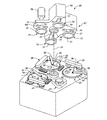
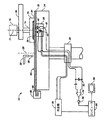
図1を参照すると、1枚以上の基板10をCMP装置20により研磨しうることが分かる。同様の研磨装置についての記載が米国特許第5,738,574号にあり、その全開示内容は参照によりこの明細書に組み入れられる。研磨装置20は、一連の研磨ステーション22a,22b及び22c並びに搬送ステーション23を含んでいる。搬送ステーション23は、基板をキャリアヘッド及びローディング装置間に搬送する。
Referring to FIG. 1, it can be seen that one or
各研磨ステーションは、回転可能のプラテン24を含んでおり、その上に研磨パッド30が置かれる。第1及び第2の研磨ステーション22a,22bは、耐久性のある硬質外表面をもつ二層研磨パッドか、或いは研磨粒子を埋め込んだ固定研粒パッドを含むことができる。最後の研磨ステーション22cは、比較的に軟質のパッド又は二層研磨パッドを含むことができる。また、各研磨ステーションは、研磨パッドが効果的に基板を研磨するように同研磨パッドの状態を維持するため、パッド状態調節装置28も含むことができる。
Each polishing station includes a
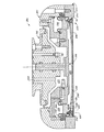
図3Aを参照すると、二層研磨パッド32は、プラテン24の表面に当接する裏当て層32と、基板10を研磨するのに使用される被覆層34とを有するのが一般的である。被覆層34は裏当て層32よりも概して硬い。しかし、パッドのなかには、被覆層のみを有し、裏当て層のないものがある。被覆層34は、例えば中空微小球であるフィラーを多分含む発泡もしくは注型ポリウレタン、及び/又は溝付き表面層から構成することができる。裏当て層32は、ウレタンに浸した圧縮フェルト繊維から構成することができる。IC−1000からなる被覆層及びSUBA−4からなる裏当て層を有する二層研磨パッドは、米国デラウェア州ニューアークのロデール・インコーポレイテッド(Rodel, Inc.)から入手できる(IC−1000及びSUBA−4は、Rodel, Inc.の製品名である)。
Referring to FIG. 3A, the two-
研磨工程中、液体(例えば、酸化研磨のために脱イオン水)とpH調整剤(例えば、酸化研磨のために水酸化カリウム)とを含有するスラリー38をスラリー供給ポートもしくはスラリー/リンス混合アーム39により研磨パッド30の表面に供給することができる。研磨パッド30が標準パッドであれば、スラリー38は、研磨粒子(例えば、酸化研磨のために二酸化ケイ素)も含有することができる。
During the polishing process, a
図1に戻ると、多重ヘッド付き回転台60は、4個のキャリヤヘッド70を支持している。この回転台は、キャリヤヘッド系とそこに取り付けられた基板とが研磨ステーション22及び搬送ステーション23間を回るように、回転台用モータ組立体(図示せず)により回転台軸線64を中心として中央支柱62によって回転される。キャリヤヘッド系のうちの3つが基板を受けて保持し、それらを研磨パッドに圧接することにより研磨する。一方、キャリヤヘッド系のうちの1つは搬送ステーション23から基板を受けると共に、搬送ステーション23に基板を配送する。
Returning to FIG. 1, the
各キャリヤヘッド70は、キャリヤ駆動軸74によりキャリヤヘッド回転モータ76(カバー68の4分の1を除去して示されている)に接続されているので、各キャリヤヘッド70をその軸線回りに独立して回転させることができる。その上、各キャリヤヘッド70は、回転台支持プレート66に形成された半径方向のスロット72において独立して横方向に往復動する。適当なキャリヤヘッド70についての記載は、西暦1999年12月23日及び西暦2000年3月27日にそれぞれ出願された米国特許願第09/470,820号及び第09/535,575号にあり、その全開示内容は参照によりこの明細書に組み入れられる。作動中、プラテンはその軸線25の回りに回転され、そしてキャリヤヘッドは、その中心軸線71の回りに回転されると共に、研磨パッドの表面に交叉して横方向に平行移動される。
Each
上述の特許出願に開示されているように、また、図2に示すように、典型的なキャリヤヘッド70は、ハウジング202、基部アセンブリ204、ジンバル機構206(これは基部アセンブリ204の一部と考えることができる)、ロードチャンバ208、保持リング210及び基板裏当てアセンブリ212を含んでおり、該基板裏当てアセンブリには、上部浮動チャンバ236、下部浮動チャンバ234及び外側チャンバ238のような3つの加圧可能なチャンバが含まれている。ロードチャンバ208は、ハウジング202及び基部アセンブリ204の間に配置されており、ロードを基部アセンブリ204に加えて、その垂直方向の位置を制御する。第1の圧力調整器(図示せず)を通路232によりロードチャンバ208に流体接続して、該ロードチャンバにおける圧力と基部アセンブリ204の垂直方向位置とを制御することができる。
As disclosed in the above-mentioned patent application and as shown in FIG. 2, a
基板裏当てアセンブリ212は、可撓性の内側メンブレン216と、可撓性の外側メンブレン218と、内側支持構造220と、外側支持構造230と、内側スペーサリング222と、外側スペーサリング232とを含んでいる。可撓性の内側メンブレン216は、制御可能な領域にあるウェーハ10に圧力を加える中央部を含む。基部アセンブリ204と内側メンブレン216との間にあり内側フラップにより封止された体積は、加圧可能の下部浮動チャンバ234を形成する。基部アセンブリ204及び内側メンブレン216の間にあって内側フラップ244及び外側フラップ246により封止された環状の体積は、加圧可能の上部浮動チャンバ236を画成する。内側メンブレン216と外側メンブレン218との間に封止された体積は、加圧可能の外側チャンバ238を画成する。3個の圧力調節器(図示せず)は、下部浮動チャンバ234、上部浮動チャンバ236及び外側チャンバ238に個別に接続することができる。従って、ガスのような流体を各チャンバの中に、或いは外に個別に案内することができる。
The
下部浮動チャンバ234、上部浮動チャンバ236及び外側チャンバ238における圧力の組合せで、外側メンブレン218の頂面に対する内側メンブレン216の圧力と接触面積との双方を制御する。例えば、流体を上部浮動チャンバ236外に圧送することにより、内側メンブレン216の縁が持ち上げられて外側メンブレン218から離れ、そのため、内側メンブレン及び外側メンブレン間の接触領域の接触直径Dcが減少する。逆に、流体を上部浮動チャンバ236内に圧送することにより、内側メンブレン216の縁が外側メンブレン218に向かって下降し、そのため、接触領域の接触直径Dcが大きくなる。また、流体を下部浮動チャンバ234の内部又は外部に圧送することにより、外側メンブレン218に対する内側メンブレン216の圧力。従って、キャリヤヘッドによって負荷された領域における圧力のほかに、その領域の直径も制御することができる。
The combination of pressure in the lower floating chamber 234, upper floating
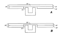
図3A及び3Bを参照すると、凹部26がプラテン24に形成され、透明部36が下に凹部26のある研磨パッド30に形成されている。この開口26及び透明部36は、キャリヤヘッドの平行移動位置に関係なく、プラテンの回転中のある一部分の間、基板10の直下を通るように、位置決めされている。研磨パッド32が二層パッドであると仮定すれば、裏当て層32の一部を除去して被覆層34に透明プラグ36を挿入することによって、薄いパッド部36を構成することができる。このプラグ36は、比較的に純粋なポリマー又はポリウレタンでよく、例えば、フィラーなしに形成されうる。一般に、透明部36の材料は非磁性かつ非導電性でなければならない。
Referring to FIGS. 3A and 3B, a
図3A及び図4を参照すると、第1の研磨ステーション22aは、現場での渦電流監視システム40と光学監視システム140とを含んでいる。現場での渦電流監視システム40及び光学監視システム140は、研磨プロセス制御及び終点検出システムとして機能することができる。第2の研磨ステーション22b及び最終の研磨ステーション22cは共に光学監視システムだけを含むことができるが、どちらも渦電流監視システムを追加的に含んでいてよい。
Referring to FIGS. 3A and 4, the first polishing
渦電流監視システム40は、基板の金属層に渦電流を誘起するための駆動システム48と、この駆動システムにより金属層に誘起された渦電流を検出するための検出システム58とを含んでいる。監視システム40は、プラテンと共に回転するように凹部26内に配置された磁心42と、この磁心42の一部分に巻回された駆動コイル44と、磁心42の第2部分に巻回された検出コイル46とを含んでいる。駆動システム48のため、監視システム40は、駆動コイル44に接続された発振器50を含んでいる。検出システム58のために、監視システム40は、検出コイル46と並列に結合されたキャパシタ52と、検出コイル46に結合されたRF増幅器54と、ダイオード56とを含んでいる。発振器50、キャパシタ52、RF増幅器54及びダイオード56は、プラテン24から離間して配置することができると共に、回転電気継手29を介してプラテンの諸要素と接続することができる。
The eddy
図5を参照するに、作動中、発振器50は駆動コイル44を駆動して、磁心42の本体から広がってその2つの磁極42a,42b間のギャップ46に入る振動磁界48を発生する。この磁界48の少なくとも一部は、研磨パッド30の薄い部分を通って広がり基板10に入る。金属層12が基板10上にあれば、振動磁界48はこの金属層12に渦電流を発生させる。渦電流は、金属層12を検出コイル46及びキャパシタ52と並列のインピーダンス源として作用させる。金属層の厚さが変化するにつれて、インピーダンスが変化し、その結果、検出機構のQ係数に変化が生じる。検出機構のQ係数の変化を検出することによって、渦電流センサは渦電流の強度変化を検出し、従って、金属層12の厚さの変化を検出する。
Referring to FIG. 5, in operation, the
図6を参照すると、磁心42は、比較的に高い透磁率(例えば、約2500)の非導電性材料で形成されたU形の本体とすることができる。特に、磁心42はフェライトでよい。一実施例において、2つの磁極42a及び42bは約0.6インチ離れており、磁心42は約0.6インチの奥行きがあり、そして磁心の横断面は一辺が0.2インチの正方形である。
Referring to FIG. 6, the
一般に、現場での渦電流監視システム40は、約50kHz〜10MHz、例えば2MHzの共振周波数を有するように構成される。例えば、検出コイル46は、約0.3〜30μHのインダクタンスを有していてよく、キャパシタ52は約0.2〜20nFのキャパシタンスを有していてよい。駆動コイルは発振器からの駆動信号に適応するように設計することができる。例えば、発振器が低電圧かつ低インピーダンスを有している場合、駆動コイルは、巻数をもっと少なくして小さなインダクタンスとすることができる。それに対して、発振器が高電圧かつ高インピーダンスを有している場合、駆動コイルは、巻数をもっと多くして大きなインダクタンスとすることができる。
Generally, the on-site eddy
一実施例において、検出コイル46は磁心の各アーム部に巻回された9巻きを有し、駆動コイル44は磁心の基部に巻回された2巻きを有し、そして発振器は約0.1V〜5.0Vの振幅で駆動コイル44を駆動する。また、一実施例において、検出コイルが約2.8μHのインダクタンスを有しており、キャパシタ52は約2.2nFのキャパシタンスを有し、そして共振周波数は約2MHzである。もう一つの実施例において、検出コイルは約3μHのインダクタンスを有しており、キャパシタ52は約400pFのキャパシタンスを有している。勿論、これらの値は、正確な巻き構造、磁心組成及び形状、並びにキャパシタのサイズの影響を大きく受けるので、単なる一例である。
In one embodiment, the
一般に、導電膜の予想初期厚さが厚ければ厚いほど、希望共振周波数は低くなる。例えば、一例として2000オングストロームのような比較的に薄い膜については、キャパシタンス及びインダクタンスは、比較的に高い共振周波数、例えば約2MHzを発生するように選択できる。これに反して、例えば2000オングストロームのように比較的に厚い膜については、キャパシタンス及びインダクタンスは、例えば約50kHzという比較的に低い共振周波数を発生するように選択できる。しかし、厚い銅の層では高い共振周波数が依然として功を奏することになる。また、キャリヤヘッドにおける金属部材からのバックグラウンドノイズを減らすために非常に高い周波数(約2MHz)を使用することができる。 In general, the thicker the expected initial thickness of the conductive film, the lower the desired resonant frequency. For example, for a relatively thin film such as 2000 angstroms as an example, the capacitance and inductance can be selected to generate a relatively high resonant frequency, eg, about 2 MHz. On the other hand, for a relatively thick film, for example 2000 angstroms, the capacitance and inductance can be selected to produce a relatively low resonant frequency, for example about 50 kHz. However, a high resonant frequency will still work for thick copper layers. Also, a very high frequency (approximately 2 MHz) can be used to reduce background noise from metal members in the carrier head.
図3A、図4及び図7Aを参照すると、最初、研磨を行う前、発振器50は基板が存在しない状態でLC回路の共振周波数に同調される。この共振周波数はRF増幅器54からの出力信号を最大振幅にすることになる。
Referring to FIGS. 3A, 4 and 7A, first, before polishing, the
図7B及び図8に示すように、研磨工程のため、基板10が研磨パッド30との接触状態に置かれる。基板10は、シリコンウェーハ12と、例えば銅のような金属である導体層16とを含み、この導体層16は、半導体、導体又は絶縁体層とすることができる1層以上の下側のパターン層14を覆って配置されている。タンタル又は窒化タンタルのようなバリヤ層18により金属層を下側の誘電体から分離させうる。下側のパターン層は、例えば、バイア、パッド及び相互接続のような金属特徴を含むことができる。研磨の前、導体層16のバルクは、当初、比較的に厚くかつ連続しているので、比較的に小さな固有抵抗を有しており、比較的に強い渦電流を導体層に発生させることができる。前述したように、渦電流は、金属層を検出コイル46及びキャパシタ52と並列のインピーダンス源として作用させる。その結果、導体層16の存在により検出回路のQ係数が減少し、それによりRF増幅器56からの信号の振幅が著しく減じる。
As shown in FIGS. 7B and 8, the
図7C及び図8を参照するに、基板10が研磨されるにつれて、導体層16のバルク部が薄くなる。導体層16が薄肉化するため、その面積抵抗が上昇し、金属層における渦電流は減衰するようになる。その結果、金属層16及び検出回路58間の結合が減じる(仮想インピーダンス源の固有抵抗の増大)。結合が低下するため、検出回路58のQ係数はその当初の値に向かい増大する。
Referring to FIGS. 7C and 8, as the
図7D及び図8を参照すると、最終的に、導体層16のバルク部は除去され、絶縁性のパターン層14との間のトレンチに相互接続16’が残る。この時点で、該して小さくかつ該して非連続である基板の諸導体部と検出回路58との間の結合が最小になる。その結果、検出回路のQ係数は最大値に達する(基板が全く存在しないときのQ係数の値ほど大きくはない)。これにより、検出回路からの出力信号の振幅を頭打ち状態にさせる。
Referring to FIGS. 7D and 8, finally, the bulk portion of the
従って、出力信号の振幅がもはや増大せず安定した時点(例えば、局所的に横這いもしくは水平状態に達した時点)を検出することにより、コンピュータ90は、研磨終点を検出することができる。或いは、1枚以上のテスト基板を研磨することにより、研磨機械のオペレータは、金属層の厚さの関数として出力信号の振幅を測定することができる。従って、終点検出器は、特定厚さの金属層が基板上に残っているときに研磨を中止させることができる。特に、コンピュータ90は、増幅器からの出力信号が所望厚さに対応する電圧スレッショルドを超えるときに終点をトリガーすることができる。或いは、渦電流監視システムも研磨パラメータの変化をトリガーするのに使用できる。例えば、渦電流監視システムが研磨基準を検出したときに、CMP装置は、スラリー組成を変更することができる(例えば、高選択性のスラリーから低選択性のスラリーへ)。別の例として、以下に述べるように、CMP装置は、キャリヤヘッドにより加えられる圧力分布を変えることができる。
Accordingly, the
図9Aを参照すると、渦電流監視システムは、振幅の変化を検出することに加えて、検出した信号の位相シフトを演算するための位相シフト検出器を含むことができる。金属層が研磨されるので、検出した信号の位相は発振器50からの駆動信号に関して変化する。この位相差は研磨された層の厚さに相関付けることができる。
Referring to FIG. 9A, the eddy current monitoring system can include a phase shift detector for computing the phase shift of the detected signal in addition to detecting the change in amplitude. As the metal layer is polished, the phase of the detected signal changes with respect to the drive signal from the
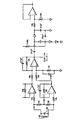
渦電流監視システムの振幅及び位相シフトの双方に関する部分の実施例が図9Bに示されている。この実施例は、図9Bに示すように、駆動信号及び検出信号を結合して、位相差に比例するパルス幅又はデューティーサイクルをもつ位相シフト信号を発生する。この実施例においては、2つのXORゲート100及び102を使用して、検出コイル46及び発振器50からの正弦波信号をそれぞれ方形波信号に変換する。2つの方形波信号は第3のXORゲート104の入力に供給される。第3のXORゲート104の出力は、2つの方形波信号間の位相差に比例するパルス幅又はデューティーサイクルをもつ位相シフト信号である。この位相シフト信号は、RCフィルタ106によってろ過され、位相差に比例する電圧を有するDC的な信号を発生する。或いは、該信号は、位相シフト測定を行うプログラマブル・ディジタル・ロジック、例えば、結合プログラム可能論理デバイス(CPLD)又は書替え可能ゲートアレイ(FGPA)に入力することができる。渦電流監視システムの振幅検出部分のもう一つの実施例は図9Cに示されている。駆動信号及び検出信号間の位相差を測定する渦電流監視システムにより発生されるトレースの例は図10に示されている。位相測定は駆動周波数の安定性に非常に敏感に反応するから、位相ロックループ電子回路を付加しうる。
An example of a portion relating to both amplitude and phase shift of an eddy current monitoring system is shown in FIG. 9B. In this embodiment, as shown in FIG. 9B, the driving signal and the detection signal are combined to generate a phase shift signal having a pulse width or duty cycle proportional to the phase difference. In this embodiment, two
考えうる位相差測定の利点は、金属層の厚さに関する位相差の相関関係が振幅のそれよりももっと線形になりうることである。また、その上、金属層の絶対厚さが考えられる広範囲の厚さにわたり測定しうる。 A possible phase difference measurement advantage is that the correlation of the phase difference with respect to the thickness of the metal layer can be more linear than that of the amplitude. Moreover, the absolute thickness of the metal layer can be measured over a wide range of possible thicknesses.
図3Aに戻ると、反射率計又は干渉計として機能しうる光学監視システム140は、渦電流監視システム40に隣接して凹部26中でプラテン24に固定することができる。従って、光学監視システム140は、渦電流監視システム40により監視されているのと実質的に同じ基板上の位置の反射率を測定することができる。特に、光学監視システム140は、プラテン24の回転軸線から渦電流監視システム40と同一の半径方向距離のところにある基板の一部を測定するように位置決めしうる。従って、光学監視システム140は、渦電流監視システム40と同じ通路において基板を掃引もしくは走査することができる。
Returning to FIG. 3A, an
光学監視システム140は、光源144及び検出器146を含んでいる。光源は、透明窓部36及びスラリーを通って拡散し基板10の露出面に衝突する光ビーム142を発生する。例えば、光源144はレーザーでよく、光ビーム142は平行レーザービームでよい。光レーザビーム142は、基板10の表面に対して直角の軸線からある角度をなしてレーザー144から発射することができる。また、孔26及び窓36が細長ければ、ビーム拡大器(図示せず)を光ビームの通路に配置して、窓の長手方向軸心に沿って光ビームを拡大することができる。一般的に、光学監視システムは、米国特許第6,159,073号及び1998年11月2日に出願された米国特許願第09/184,767号に記載されたように機能し、それらの全開示内容は参照により本明細書に組み入れられる。
The
図11は、駆動信号及び検出信号間の位相差を測定する光学監視システムによって発生されたトレース250の一例を示している。強度トレース250の全形状について以下に説明する。最初、金属層16は、下側にあるパターン層14のトポロジーのため、ある初期トポグラフィーを有している。このトポグラフィーのため、光ビームは金属層に衝突すると散乱する。研磨工程がトレースの部分252で進むにつれて、金属層はより平坦になり、研磨された金属層の反射率が増大する。金属層のバルクがトレースの部分254において除去されるので、強度は比較的に安定したままである。一旦酸化層がトレースにおいて露出し始めると、全信号強度はトレースの部分256において急激に低下する。一旦酸化層がトレースにおいて完全に露出すると、強度はトレースの部分258において再び安定するが、酸化層が除去される際の干渉効果により、強度は僅かな振動を受けることがある。
FIG. 11 shows an example of a
図3A、3B及び4に戻ると、CMP装置20は、磁心42及び光源44がいつ基板10の直下にあるかを検出するため、光学的断続器のような位置センサ80を含みうることが分かる。例えば、光学的断続器は、キャリヤヘッド70に向き合った一定位置に装着しうる。プラテンの外周には遮光板82が取り付けられている。遮光板82の取付位置及び長さは、透明部36が基板10の直下を通っている間にセンサ80の光信号を遮断するように、選択されている。或いは、CMP装置は、プラテンの角位置を測定するためのデコーダを含むことができる。
Returning to FIGS. 3A, 3B and 4, it can be seen that the
多目的プログラム可能ディジタルコンピュータ90は、渦電流監視システムからの強度信号及び位相シフト信号を受けると共に、光学監視システムからの強度信号を受ける。これらの監視システムはプラテンの各回転ごとに基板の直下を掃引もしくは走査するので、金属層の厚さ及び下側にある層の露出に関する情報は、連続実時間方式(プラテン1回転ごとに1回)で現場集積される。コンピュータ90は、基板が透明部36の大体上にあるときに(位置センサにより求められる)監視システムからの信号をサンプリングするようにプログラムすることができる。研磨が進行するにつれて、金属層の反射率又は厚さが変わり、サンプリングされた信号は時間と共に変化する。時間と共に変化する該サンプリングされた信号はトレースと呼ばれることがある。監視システムからの測定値は、研磨中、出力装置92に表示することができ、装置のオペレータが研磨工程の進行を目視により監視することを可能としている。また、以下に述べるように、トレースは研磨プロセスを制御すると共に金属層の研磨工程の終点を求めるために使用しうる。
The multipurpose programmable
渦電流監視システム40及び光学監視システム140の双方からの信号がコンピュータ90に入力されるので、これら監視システムの一方又は双方を終点判断のために使用しうる。これは、化学機械研磨装置が誘電材料及び金属材料の双方を研磨するための強力な終点検出能力をもつことを可能にする。これら双方のシステムからの信号は、終点基準を求めて監視することができ、双方のシステムからの終点基準の検出を種々のブール論理演算(例えば、AND又はOR)と組み合わせて、プロセスパラメータの変化又は研磨終点をトリガーさせることができる。検出器論理のための可能なプロセス制御及び終点基準には、極大又は極小、勾配の変化、振幅又は勾配のスレッショルド値、或いはそれらの組合せが含まれる。一方の監視システムが他方の監視システムを確認するのに役立つようにしうる。例えば、研磨装置は、渦電流信号及び光強度信号の双方の適切な終点基準を検出した際にのみ研磨を中止しうる。或いは、一方のシステムバックアップの終点検出器として作用しうる。例えば、研磨装置は、一方のシステム、例えば渦電流監視システムからの第1の終点基準を検出した際にのみ研磨を中止でき、終点基準がある時間フレームで検出されなければ、研磨は、他方のシステム、例えば光学監視システムからの第2の終点基準を検出した際に中止できる。加えて、これら2つのシステムは研磨工程の異なる部分の間に使用できる。例えば、金属研磨(特に銅の研磨)中、基板の大部分は、渦電流監視システムによる監視を受けながら、研磨されうる。
Since signals from both the eddy
金属層の研磨工程において、CMP装置20は、渦電流監視システム40及び光学監視システム140を使用して、フィラー層(filler layer)のバルクがいつ除去されたか、及び下側の阻止層(stop layer)がいつ実質的に露出したのかを決定する。コンピュータ90は、プロセス制御及び終点検出ロジックをサンプリングした信号に適用して、プロセスパラメータをいつ変更するか、及び研磨終点をいつ検出するか決定する。金属層が所定厚さに達したことを渦電流監視システムが決定したときに、光学監視システムを使用して、下側の絶縁層がいつ露出されたのかを求めることができる。
In the polishing process of the metal layer, the
また、コンピュータ90は、1999年12月13日に出願された米国特許願第09/460,529号に述べられているように、基板下の各走査による渦電流監視システム40及び光学監視システム140の双方からの測定値を複数のサンプリングゾーン96に分割して、各サンプリングゾーンの半径方向位置を演算し、振幅測定値を複数の半径方向範囲に分け、各サンプリングゾーンについて最小、最大及び平均測定値を求め、多重半径方向範囲を使用して研磨終点を求めるようにプログラムすることができ、該米国特許願の開示内容は参照によりこの明細書に組み入れられる。
The
また、コンピュータ48は、キャリヤヘッド70により加えられる圧力を制御する圧力機構、キャリヤヘッド回転速度を制御するキャリヤヘッド回転モータ76、プラテン回転速度を制御するプラテン回転モータ(図示せず)、又は研磨パッドに供給されるスラリー組成を制御するスラリー配送システム39に接続することもできる。特に、2000年7月5日に出願の米国特許願第09/609,426号に述べられているように、測定値を複数の半径方向範囲に分けた後、金属層の厚さに関する情報は、キャリヤヘッドにより加えられる研磨圧力のプロフィールを周期的に又は連続的に修正するため閉ループコントローラに実時間で入力することができ、該米国特許願の開示内容は参照によりこの明細書に組み入れられる。例えば、コンピュータは、終点基準が外側の半径方向範囲については満たされているが内側の半径方向範囲については満たされていないことを決定できる。これは、下側にある層が環状の外側領域において露出しているが内側領域では露出していないことを示している。この場合、コンピュータは、圧力が加えられる領域の直径を減少させて、基板の内側領域にのみ圧力を加えるようにすることができ、これにより基板の外側領域に関するエロージョン及びわん状変形が軽減される。
The
銅層のような金属層を研磨する方法は、図12にフローチャートの形式で示されている。先ず、第1の研磨ステーション22aで基板を研磨して金属層のバルクを除去する。研磨プロセスは渦電流監視システム40により監視する。例えば2000オングストロームである所定厚さの銅層14が下側のバリヤ層16(図 を参照)を覆い残っているときに、研磨プロセスを中止して、基板を第2の研磨ステーション22bに搬送する。この最初の研磨終点は、位相シフト信号が実験的に決められるスレッショルド値を超えたときに、トリガーすることができる。第1の研磨ステーションについての具体例としての研磨パラメータには、プラテン回転速度93rpm、キャリヤヘッド圧力約3psi及びIC−1010研磨パッドが挙げられる。第1の研磨ステーションで研磨が進行するにつれて、渦電流監視システム40からの半径方向厚さ情報を閉ループフィードバックシステムに入力し、基板に関するキャリヤヘッド200のローディング面積及び/又は圧力を制御することができる。研磨パッドにかかる保持リングの圧力も調節して研磨速度を制御しうる。これにより、キャリヤヘッドは、研磨速度の非一様性に対して、或いは入来する基板の金属層の厚さの非一様性に対して補償することが可能になる。その結果、第1の研磨ステーションでの研磨後、金属層の大部分が除去され、基板上に残存している金属層の表面は実質的に平坦化される。
A method for polishing a metal layer, such as a copper layer, is illustrated in flowchart form in FIG. First, the substrate is polished at the
第2の研磨ステーション22bでは、基板は、第1の研磨ステーションよりも遅い研磨速度で研磨される。例えば、研磨速度は約2分の1〜4分の1に、即ち約50%〜75%だけ減少される。研磨速度を減少させるため、キャリヤヘッド圧力を下げてよいし、キャリヤヘッド回転速度を下げてよいし、スラリーの組成を変更して低研磨のスラリーを導入してよいし、及び/又はプラテン回転速度を下げてもよい。例えば、キャリヤヘッドから基板にかかる圧力は約33%〜50%減少させ、プラテン回転速度及びキャリヤヘッド回転速度は双方とも約50%減少させうる。第2の研磨ステップ22bにおける具体例としての研磨パラメータには、プラテン回転速度43rpm、キャリヤヘッド圧力約2psi及びIC−1010研磨パッドが挙げられる。 In the second polishing station 22b, the substrate is polished at a slower polishing rate than in the first polishing station. For example, the polishing rate is reduced by about one-fourth, that is, by about 50% to 75%. To reduce the polishing rate, the carrier head pressure may be reduced, the carrier head rotation rate may be reduced, the slurry composition may be altered to introduce a low polishing slurry, and / or the platen rotation rate. May be lowered. For example, the pressure on the substrate from the carrier head can be reduced by about 33% to 50%, and both the platen rotation speed and the carrier head rotation speed can be reduced by about 50%. Exemplary polishing parameters in the second polishing step 22b include a platen rotation speed of 43 rpm, a carrier head pressure of about 2 psi, and an IC-1010 polishing pad.
第2の研磨ステーションで研磨を開始する場合、随意であるが、例えば約10秒間、3psiのような幾分高い圧力で、例えば93rpmのプラテン回転速度で基板を短時間研磨することができる。“開始”ステップと呼ぶことができるこの初期研磨は、金属層に形成された自然酸化物を除去するため、或いは予定スループットを維持するようにプラテン回転速度及びキャリヤヘッド圧力の立上げについて補償するため、必要になることがある。 Optionally, when starting polishing at the second polishing station, the substrate can be polished for a short time at a somewhat higher pressure, such as 3 psi, for example, for about 10 seconds, at a platen rotation rate of, for example, 93 rpm. This initial polishing, which can be referred to as the “start” step, removes the native oxide formed in the metal layer, or to compensate for the rise in platen rotation speed and carrier head pressure to maintain a predetermined throughput. , May need.
研磨プロセスは、光学監視システムにより第2の研磨ステップ22bで監視される。第2の研磨ステーション22bでの研磨は、金属層が除去されて下側のバリヤ層が露出するまで、進められる。勿論、金属層のほんの一部は基板上に残留していてよいが、金属層は実質的に完全に除去される。光学監視システムは、バリヤ層が露出するときの反射率の変化を検出できるので、その終点を決めるのに有効である。特に、第2の研磨ステーションについての終点は、光学監視信号の振幅又は勾配がコンピュータにより監視される全半径方向範囲で実験的に決められるスレッショルド値よりも低下したときに、トリガーすることができる。これは、バリヤ金属層が基板の実質的に全てにわたり除去されたことを示している。勿論、研磨が第2の研磨ステーション22bで進行するときに、光学監視システム40からの反射率情報を閉ループフィードバックシステムに入力して、基板に関するキャリヤヘッド200のローディング面積及び/又は圧力を制御し、最先に露出されるバリヤ層の諸範囲が過度に露出するのを防止することができる。
The polishing process is monitored at the second polishing step 22b by an optical monitoring system. Polishing at the second polishing station 22b proceeds until the metal layer is removed and the lower barrier layer is exposed. Of course, only a portion of the metal layer may remain on the substrate, but the metal layer is substantially completely removed. The optical monitoring system can detect the change in reflectance when the barrier layer is exposed, and is effective in determining the end point. In particular, the end point for the second polishing station can be triggered when the amplitude or slope of the optical monitoring signal falls below a threshold value determined experimentally over the entire radial range monitored by the computer. This indicates that the barrier metal layer has been removed over substantially all of the substrate. Of course, as polishing proceeds at the second polishing station 22b, reflectivity information from the
バリヤ層が露出する前に研磨速度を減じることにより、わん状変形及びエロージョンの影響を低減することができる。その上、研磨装置の相対的な反応時間(reaction time)が改善され、研磨装置が、最後の終点基準が検出された後に除去される材料をもっと少なくして、研磨を中止し第3の研磨ステーションに送ることを可能にする。更に、大抵の強度測定値を予想研磨終了時間近くで補正することができ、そのため研磨終点演算の精度を向上させる可能性がある。しかしながら、第1の研磨ステーションにおける研磨工程の大部分にわたり高研磨速度を維持することにより、高スループットが達成される。キャリヤヘッド圧力が減少される前に、或いは他の研磨パラメータが変更される前に、金属層のバルク研磨の少なくとも75%、例えば80〜90%が終了していることが好ましい。 By reducing the polishing rate before the barrier layer is exposed, the effects of wrinkle deformation and erosion can be reduced. In addition, the relative reaction time of the polisher is improved so that the polisher stops the third polish with less material removed after the last endpoint criterion is detected Allows sending to station. Furthermore, most intensity measurements can be corrected near the expected polishing end time, which may improve the accuracy of the polishing end point calculation. However, high throughput is achieved by maintaining a high polishing rate over most of the polishing process at the first polishing station. It is preferred that at least 75%, for example 80-90%, of the bulk polishing of the metal layer is completed before the carrier head pressure is reduced or other polishing parameters are changed.
一旦第2の研磨ステーション22bで金属層が除去されたら、バリヤ層を除去するため、基板は第3の研磨ステーション22cに搬送される。第2の研磨ステーションについての具体例としての研磨パラメータには、プラテン回転速度103rpm、キャリヤヘッド圧力約3psi及びIC−1010研磨パッドが挙げられる。随意であるが、基板は、開始ステップでは、例えば約5秒間、3psiのような幾分高い圧力で、例えば103rpmのプラテン回転速度で短時間研磨することができる。この研磨プロセスは、光学監視システムにより第3の研磨ステーションで監視されており、バリヤ層が実質的に除去され下側の導体層が実質的に露出されるまで、続行される。第1及び第2の研磨ステーションでは同じスラリー溶液を用いてよいが、それに対して第3の研磨ステーションでは別のスラリー溶液を用いることができる。 Once the metal layer is removed at the second polishing station 22b, the substrate is transferred to the third polishing station 22c to remove the barrier layer. Exemplary polishing parameters for the second polishing station include a platen rotation speed of 103 rpm, a carrier head pressure of about 3 psi, and an IC-1010 polishing pad. Optionally, the substrate can be polished in the starting step for a short period of time, for example about 5 seconds, with a somewhat higher pressure, such as 3 psi, for example, a platen rotation rate of 103 rpm. This polishing process is monitored at a third polishing station by an optical monitoring system and continues until the barrier layer is substantially removed and the underlying conductor layer is substantially exposed. The same slurry solution may be used at the first and second polishing stations, whereas another slurry solution may be used at the third polishing station.
銅層のような金属層を研磨する代替方法が図13にフローチャートの形式で示されている。この方法は図12に記載した方法と類似している。しかし、第1の研磨ステーション22aでは急速研磨ステップ及び遅速研磨ステップの双方が行われる。バリヤ層の除去は第2の研磨ステーション22bで行われ、バフ研磨ステップは最終の研磨ステーション22cで行われる。
An alternative method of polishing a metal layer such as a copper layer is shown in flowchart form in FIG. This method is similar to the method described in FIG. However, both the rapid polishing step and the slow polishing step are performed at the
渦電流監視システム及び光学監視システムは種々の研磨システムで使用することができる。研磨パッド又はキャリヤヘッドのどちらか一方、或いは双方は、研磨表面及び基板間に相対運動を与えるために可動である。研磨パッドは、プラテンに取り付けられた円形(又はその他のある形状)のパッド、供給ロール及び巻取りロール間に延在するテープ、又は連続ベルトでよい。研磨パッドは、プラテンに付着されるか、研磨工程間をプラテン上で増分的に進められるか、或いは研磨中プラテン上で連続的に駆動されるかすることができる。パッドは、研磨中にプラテンに取着することができ、或いは研磨中にプラテン及び研磨パッド間に流体軸受が存在してよい。研磨パッドは、標準(例えば、フィラーがあるか又はないポリウレタン)の粗いパッドか、軟質パッドか、或いは研磨材固定のパッドとすることができる。発振器の駆動周波数は、基板が存在しないときに波長調整するよりも、研磨済み又は未研磨の基板が存在する状態(キャリヤヘッドが在っても無くてもよい)で共振周波数に、或いはまた別の基準に同調させることができる。 Eddy current monitoring systems and optical monitoring systems can be used in various polishing systems. Either the polishing pad or the carrier head, or both, are movable to provide relative movement between the polishing surface and the substrate. The polishing pad may be a circular (or some other shape) pad attached to the platen, a tape extending between the supply roll and the take-up roll, or a continuous belt. The polishing pad can be attached to the platen, incrementally advanced on the platen between polishing steps, or continuously driven on the platen during polishing. The pad can be attached to the platen during polishing, or there can be a hydrodynamic bearing between the platen and the polishing pad during polishing. The polishing pad can be a standard (eg, polyurethane with or without filler) rough pad, a soft pad, or an abrasive fixed pad. The driving frequency of the oscillator is adjusted to the resonance frequency in the presence of a polished or unpolished substrate (with or without a carrier head), or to be adjusted, rather than adjusting the wavelength when no substrate is present. Can be tuned to the standard of
光学監視システム140は、同じ孔に位置決めされるものとして図示されているが、渦電流監視システム40とは異なるプラテン上の場所に位置決めすることができる。例えば、光学監視システム140及び渦電流監視システム40は、プラテンの両側に配置できるので、同システムは基板表面を交互に走査する。
Although the
図14を参照すると、もう一つの実施例において、第1の研磨ステーションは渦電流監視システム40のみを含み、光学監視システムを含んでいない。この場合、パッドの部分36’は透明である必要はない。しかし、部分36’は比較的に薄いことが有利である。例えば、研磨パッド30が二層パッドであると仮定した場合、薄いパッド部分36’は、裏当て層32’の一部33’を除去することにより、図15Aに示すように構成することができる。或いは、図15Bに示すように、薄いパッド部分36”は、裏当て層32”の一部33”及び被覆層34”の一部を双方とも除去することにより形成することができる。従って、この実施例は、薄いパッド部分36”において被覆層34”の底面に凹部を有している。研磨パッドが単層パッドであれば、この薄いパッド部分36は、パッド材料の一部を除去してパッドの底面に凹部を創生することにより形成することができる。研磨パッドがそれ自体十分に薄いか、或いは渦電流の測定と干渉しない透磁率(及び導電率)を有していれば、パッドは、何らの改変も或いは凹部も必要としない。
Referring to FIG. 14, in another embodiment, the first polishing station includes only the eddy
渦電流センサが単一コイルを使用していれば、基板とは反対の研磨面の側にコイルを配置したり、或いは位相差を測定するというような本発明の種々の側面も依然として適用される。単一コイルシステムにおいては、発振器及びセンスキャパシタ(sense capacitor)(及びその他のセンサ回路)の双方が同じコイルに接続される。 If the eddy current sensor uses a single coil, various aspects of the present invention still apply, such as placing the coil on the side of the polishing surface opposite the substrate or measuring the phase difference. . In a single coil system, both the oscillator and sense capacitor (and other sensor circuits) are connected to the same coil.
本発明を好適な実施例に関して説明してきた。しかし、本発明は、図示され説明された実施例に限定されるものではない。むしろ、本発明の範囲は、冒頭の特許請求の範囲により明示される。 The invention has been described with reference to the preferred embodiment. However, the invention is not limited to the embodiments shown and described. Rather, the scope of the present invention is defined by the appended claims.
10…基板、12…金属層、14…下側のパターン層、16…導体層、18…バリヤ層、20…化学機械研磨(CMP)装置、22a,22b,22c…研磨、23…搬送ステーション、24…プラテン、26…凹部、30…研磨パッド、32…裏当て層、34…被覆層、36…透明部、38…スラリー、40…渦電流監視システム、42…磁心、42a,42b…極、44…駆動コイル、48…駆動システム、46…検出コイル、50…発振器、52…キャパシタ、54…RF増幅器、56…RF増幅器、58…検出システム、70…キャリヤヘッド、76…キャリヤヘッド回転モータ、80…位置センサ、90…コンピュータ(コントローラ)、100…XORゲート、102…XORゲート、104…XORゲート、106…RCフィルタ、140…光学監視システム、142…光ビーム、144…光源、146…検出器。
DESCRIPTION OF
図3を参照すると、二層研磨パッド32は、プラテン24の表面に当接する裏当て層32と、基板10を研磨するのに使用される被覆層34とを有するのが一般的である。被覆層34は裏当て層32よりも概して硬い。しかし、パッドのなかには、被覆層のみを有し、裏当て層のないものがある。被覆層34は、例えば中空微小球であるフィラーを多分含む発泡もしくは注型ポリウレタン、及び/又は溝付き表面層から構成することができる。裏当て層32は、ウレタンに浸した圧縮フェルト繊維から構成することができる。IC−1000からなる被覆層及びSUBA−4からなる裏当て層を有する二層研磨パッドは、米国デラウェア州ニューアークのロデール・インコーポレイテッド(Rodel, Inc.)から入手できる(IC−1000及びSUBA−4は、Rodel, Inc.の製品名である)。
With reference to FIG. 3 , the two-
図3を参照すると、凹部26がプラテン24に形成され、透明部36が下に凹部26のある研磨パッド30に形成されている。この開口26及び透明部36は、キャリヤヘッドの平行移動位置に関係なく、プラテンの回転中のある一部分の間、基板10の直下を通るように、位置決めされている。研磨パッド32が二層パッドであると仮定すれば、裏当て層32の一部を除去して被覆層34に透明プラグ36を挿入することによって、薄いパッド部36を構成することができる。このプラグ36は、比較的に純粋なポリマー又はポリウレタンでよく、例えば、フィラーなしに形成されうる。一般に、透明部36の材料は非磁性かつ非導電性でなければならない。
Referring to FIG. 3 , a
図3を参照すると、第1の研磨ステーション22aは、現場での渦電流監視システム40と光学監視システム140とを含んでいる。現場での渦電流監視システム40及び光学監視システム140は、研磨プロセス制御及び終点検出システムとして機能することができる。第2の研磨ステーション22b及び最終の研磨ステーション22cは共に光学監視システムだけを含むことができるが、どちらも渦電流監視システムを追加的に含んでいてよい。
Referring to FIG. 3 , the
図3及び図7Aを参照すると、最初、研磨を行う前、発振器50は基板が存在しない状態でLC回路の共振周波数に同調される。この共振周波数はRF増幅器54からの出力信号を最大振幅にすることになる。
Referring to FIGS. 3 and 7A, first, before polishing, the
図3に戻ると、反射率計又は干渉計として機能しうる光学監視システム140は、渦電流監視システム40に隣接して凹部26中でプラテン24に固定することができる。従って、光学監視システム140は、渦電流監視システム40により監視されているのと実質的に同じ基板上の位置の反射率を測定することができる。特に、光学監視システム140は、プラテン24の回転軸線から渦電流監視システム40と同一の半径方向距離のところにある基板の一部を測定するように位置決めしうる。従って、光学監視システム140は、渦電流監視システム40と同じ通路において基板を掃引もしくは走査することができる。
Returning to FIG. 3 , an
図11は、光学監視システムによって発生されたトレース250の一例を示している。強度トレース250の全形状について以下に説明する。最初、金属層16は、下側にあるパターン層14のトポロジーのため、ある初期トポグラフィーを有している。このトポグラフィーのため、光ビームは金属層に衝突すると散乱する。研磨工程がトレースの部分252で進むにつれて、金属層はより平坦になり、研磨された金属層の反射率が増大する。金属層のバルクがトレースの部分254において除去されるので、強度は比較的に安定したままである。一旦酸化層がトレースにおいて露出し始めると、全信号強度はトレースの部分256において急激に低下する。一旦酸化層がトレースにおいて完全に露出すると、強度はトレースの部分258において再び安定するが、酸化層が除去される際の干渉効果により、強度は僅かな振動を受けることがある。
Figure 11 shows an example of a
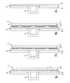
図3及び図4A〜図4Eに戻ると、CMP装置20は、磁心42及び光源44がいつ基板10の直下にあるかを検出するため、光学的断続器のような位置センサ80を含みうることが分かる。例えば、光学的断続器は、キャリヤヘッド70に向き合った一定位置に装着しうる。プラテンの外周には遮光板82が取り付けられている。遮光板82の取付位置及び長さは、透明部36が基板10の直下を通っている間にセンサ80の光信号を遮断するように、選択されている。或いは、CMP装置は、プラテンの角位置を測定するためのデコーダを含むことができる。
Returning to FIGS. 3 and 4A-4E , the
Claims (71)
前記基板に近接して位置決め可能の磁心と、
該磁心の第1部分に巻回された第1コイルと、
該第1コイルに電気的に結合されて前記第1コイルに交流を誘導すると共に前記基板に近接して交番磁界を発生させる発振器と、
前記磁心の第2部分に巻回された第2コイルと、
該第2コイルに電気的に結合されたキャパシタと、
前記第2コイル及び前記キャパシタに電気的に結合されて出力信号を発生する増幅器と、を備えるセンサ。 A sensor for monitoring a conductor film on a substrate,
A magnetic core that can be positioned close to the substrate;
A first coil wound around a first portion of the magnetic core;
An oscillator electrically coupled to the first coil to induce an alternating current in the first coil and to generate an alternating magnetic field in proximity to the substrate;
A second coil wound around the second portion of the magnetic core;
A capacitor electrically coupled to the second coil;
An amplifier electrically coupled to the second coil and the capacitor to generate an output signal.
研磨パッドと、
研磨面の第1の側に当接して基板を保持するためのキャリアと、
前記基板とは反対側の前記研磨パッドの第2の側に配置された少なくとも1つのインダクタ、該少なくとも1つのインダクタに電気的に結合されてコイルに交流を誘導すると共に交番磁界を発生させる発振器、及び前記少なくとも1つのインダクタに電気的に結合されたキャパシタを含む渦電流センサと、
前記研磨パッド及びキャリヤヘッドの少なくとも一方に接続されて両者間に相対運動を生じさせるモータと、を備える化学機械研磨装置。 A chemical mechanical polishing apparatus,
A polishing pad;
A carrier for holding the substrate in contact with the first side of the polishing surface;
At least one inductor disposed on a second side of the polishing pad opposite the substrate, an oscillator electrically coupled to the at least one inductor to induce an alternating current in the coil and generate an alternating magnetic field; And an eddy current sensor including a capacitor electrically coupled to the at least one inductor;
A chemical mechanical polishing apparatus comprising: a motor connected to at least one of the polishing pad and the carrier head to cause relative movement therebetween.
基板を研磨面の第1の側に位置決めすること、
交番磁界を前記研磨面全体に広げて前記導体層に渦電流を誘導するため、前記基板の反対側にある前記研磨面の第2の側に位置決めされたインダクタから前記交番磁界を発生させること、
前記導体層の厚さの変化により生じる前記交番磁界の変化を検出すること、を含む、導体層の厚さを監視する方法。 A method for monitoring the thickness of a conductor layer on a substrate during a polishing process,
Positioning the substrate on the first side of the polishing surface;
Generating the alternating magnetic field from an inductor positioned on a second side of the polishing surface opposite the substrate to spread an alternating magnetic field across the polishing surface to induce eddy currents in the conductor layer;
Detecting a change in the alternating magnetic field caused by a change in the thickness of the conductor layer.
導体層を有する基板を研磨面の第1の側に位置決めすること、
交番磁界を前記研磨面全体に広げて前記導体層に渦電流を誘導するため、前記基板の反対側にある前記研磨面の第2の側に位置決めされたインダクタから前記交番磁界を発生させること、
前記導体層を研磨するために前記基板及び前記研磨面間に相対運動を生じさせること、
前記基板に生じる渦電流を検出すること、
検出された前記渦電流が終点基準を示すときに研磨を中止すること、を含む化学機械研磨の方法。 A chemical mechanical polishing method,
Positioning the substrate having the conductor layer on the first side of the polishing surface;
Generating the alternating magnetic field from an inductor positioned on a second side of the polishing surface opposite the substrate to spread an alternating magnetic field across the polishing surface to induce eddy currents in the conductor layer;
Creating a relative motion between the substrate and the polishing surface to polish the conductor layer;
Detecting eddy currents generated in the substrate;
Stopping polishing when the detected eddy current indicates an endpoint criterion.
研磨面を有する研磨パッドと、
前記研磨面に当接して基板を保持するためのキャリヤと、
前記研磨パッド及びキャリヤヘッドの間に相対運動を生じさせるため前記研磨パッド及びキャリヤヘッドの少なくとも一方に接続されたモータと、
少なくとも1つのインダクタ、駆動信号を発生すると共に、前記少なくとも1つのインダクタに電気的に結合されて前記前記少なくとも1つのインダクタに交流を誘導し、交番磁界を発生する電流源、前記交番磁界を検出してセンス信号を発生するため前記少なくとも1つのインダクタに電気的に結合されたキャパシタを含むセンス回路、及び前記センス信号及び前記駆動信号間の位相差を測定するため前記電流源及び前記センス回路に接続された位相比較回路を含む導体層厚さ監視システムと、を備える化学機械研磨装置。 A chemical mechanical polishing apparatus,
A polishing pad having a polishing surface;
A carrier for holding the substrate in contact with the polishing surface;
A motor connected to at least one of the polishing pad and the carrier head to cause relative movement between the polishing pad and the carrier head;
A current source that generates at least one inductor and a drive signal, and is electrically coupled to the at least one inductor to induce an alternating current in the at least one inductor to generate an alternating magnetic field; and detects the alternating magnetic field A sense circuit including a capacitor electrically coupled to the at least one inductor to generate a sense signal and connected to the current source and the sense circuit to measure a phase difference between the sense signal and the drive signal And a conductor layer thickness monitoring system including a phase comparison circuit.
前記基板の導体層に渦電流を誘導する交番磁界を発生するため第1信号でコイルを励磁すること、
前記交番磁界を測定すると共に、該磁界を表す第2信号を発生すること、
前記第1信号及び前記第2信号を比較して両者間の位相差を決定すること、を含む方法。 A method for monitoring the thickness of a conductor layer on a substrate during a chemical mechanical polishing process, comprising:
Exciting a coil with a first signal to generate an alternating magnetic field that induces eddy currents in a conductor layer of the substrate;
Measuring the alternating magnetic field and generating a second signal representative of the magnetic field;
Comparing the first signal and the second signal to determine a phase difference therebetween.
研磨パッドと、
研磨面の第1の側に当接して基板を保持するためのキャリヤと、
前記基板の近くに交番磁界を発生するように位置決めされた渦電流監視システムと、
光ビームを発生して前記基板からの前記光ビームの反射光を検出する光学監視システムと、
前記渦電流監視システム及び前記光学監視システムからの信号を受けるコントローラと、
前記研磨パッド及びキャリヤヘッドの間に相対運動を生じさせるため前記研磨パッド及びキャリヤヘッドの少なくとも一方に接続されたモータと、を備える化学機械研磨装置。 A chemical mechanical polishing apparatus,
A polishing pad;
A carrier for holding the substrate against the first side of the polishing surface;
An eddy current monitoring system positioned to generate an alternating magnetic field near the substrate;
An optical monitoring system for generating a light beam and detecting reflected light of the light beam from the substrate;
A controller for receiving signals from the eddy current monitoring system and the optical monitoring system;
A chemical mechanical polishing apparatus comprising: a motor connected to at least one of the polishing pad and the carrier head to cause relative movement between the polishing pad and the carrier head.
研磨面の第1の側に基板を位置決めすること、
前記基板を研磨するため前記基板及び前記研磨面の間に相対運動を生じさせること、
渦電流監視システムから第1信号を発生すること、
光学監視システムから第2信号を発生すること、
終点基準を求めて前記第1信号及び前記第2信号を監視すること、を含む、化学機械研磨の方法。 A chemical mechanical polishing method,
Positioning the substrate on the first side of the polishing surface;
Creating a relative motion between the substrate and the polishing surface to polish the substrate;
Generating a first signal from the eddy current monitoring system;
Generating a second signal from the optical monitoring system;
A method of chemical mechanical polishing comprising: determining an end point criterion and monitoring the first signal and the second signal.
第1研磨ステーションにおいて前記基板を第1研磨速度で第1研磨面により研磨すること、
渦電流監視システムにより前記第1研磨ステーションにおける研磨を監視すること、
所定厚さの金属層が前記基板上に残っていることを前記渦電流監視システムが指示したときに、前記基板を第2研磨ステーションに搬送すること、
前記第2研磨ステーションにおいて前記基板を前記第1研磨速度より遅い第2研磨速度で第2研磨面により研磨すること、
光学監視システムにより前記第2研磨ステーションにおける研磨を監視すること、
第1の下側層が少なくとも部分的に露出したことを前記光学監視システムが指示したときに研磨を中止すること、を含む化学機械研磨の方法。 A method of chemical mechanical polishing a metal layer on a substrate,
Polishing the substrate with a first polishing surface at a first polishing rate at a first polishing station;
Monitoring polishing at the first polishing station by an eddy current monitoring system;
Transporting the substrate to a second polishing station when the eddy current monitoring system indicates that a metal layer of a predetermined thickness remains on the substrate;
Polishing the substrate with a second polishing surface at a second polishing rate slower than the first polishing rate at the second polishing station;
Monitoring polishing at the second polishing station by an optical monitoring system;
Stopping the polishing when the optical monitoring system indicates that the first lower layer is at least partially exposed.
第1研磨ステーションにおいて前記基板を第1研磨速度で第1研磨面により研磨すること、
渦電流監視システムにより前記第1研磨ステーションにおける研磨を監視すること、
所定厚さの金属層が前記基板上に残っていることを前記渦電流監視システムが指示したときに、前記第1研磨ステーションにおける研磨速度を減少させること、
光学監視システムにより前記第1研磨ステーションにおける研磨を監視すること、
第1の下側層が少なくとも部分的に露出したことを前記光学監視システムが指示したときに研磨を中止すること、を含む化学機械研磨の方法。 A method of chemical mechanical polishing a metal layer on a substrate,
Polishing the substrate with a first polishing surface at a first polishing rate at a first polishing station;
Monitoring polishing at the first polishing station by an eddy current monitoring system;
Reducing the polishing rate at the first polishing station when the eddy current monitoring system indicates that a metal layer of a predetermined thickness remains on the substrate;
Monitoring polishing at the first polishing station by an optical monitoring system;
Stopping the polishing when the optical monitoring system indicates that the first lower layer is at least partially exposed.
前記基板を第1研磨速度で研磨すること、
渦電流監視システムにより研磨を監視すること、
所定厚さの金属層が前記基板上に残っていることを前記渦電流監視システムが指示したときに、前記研磨速度を減じること、
光学監視システムにより研磨を監視すること、
下側層が少なくとも部分的に露出したことを前記光学監視システムが指示したときに研磨を中止すること、を含む化学機械研磨の方法。 A method of chemical mechanical polishing a metal layer on a substrate,
Polishing the substrate at a first polishing rate;
Monitoring polishing with an eddy current monitoring system;
Reducing the polishing rate when the eddy current monitoring system indicates that a metal layer of a predetermined thickness remains on the substrate;
Monitoring polishing by optical monitoring system;
Stopping polishing when the optical monitoring system indicates that the lower layer is at least partially exposed.
Applications Claiming Priority (6)
| Application Number | Priority Date | Filing Date | Title |
|---|---|---|---|
| US09/574,008 | 2000-05-19 | ||
| US09/574,008 US6924641B1 (en) | 2000-05-19 | 2000-05-19 | Method and apparatus for monitoring a metal layer during chemical mechanical polishing |
| US21722800P | 2000-07-10 | 2000-07-10 | |
| US60/217,228 | 2000-07-10 | ||
| US22166800P | 2000-07-27 | 2000-07-27 | |
| US60/221,668 | 2000-07-27 |
Related Parent Applications (1)
| Application Number | Title | Priority Date | Filing Date |
|---|---|---|---|
| JP2012221417A Division JP5778110B2 (en) | 2000-05-19 | 2012-10-03 | Field end point detection and process monitoring method and apparatus for chemical mechanical polishing |
Publications (2)
| Publication Number | Publication Date |
|---|---|
| JP2014209643A true JP2014209643A (en) | 2014-11-06 |
| JP5980843B2 JP5980843B2 (en) | 2016-08-31 |
Family
ID=27396396
Family Applications (4)
| Application Number | Title | Priority Date | Filing Date |
|---|---|---|---|
| JP2001585991A Expired - Fee Related JP5542293B2 (en) | 2000-05-19 | 2001-05-18 | Field end point detection and process monitoring method and apparatus for chemical mechanical polishing |
| JP2012221417A Expired - Lifetime JP5778110B2 (en) | 2000-05-19 | 2012-10-03 | Field end point detection and process monitoring method and apparatus for chemical mechanical polishing |
| JP2014121990A Expired - Lifetime JP5980843B2 (en) | 2000-05-19 | 2014-06-13 | Polishing control method and apparatus having eddy current monitoring system and optical monitoring system |
| JP2014121991A Expired - Lifetime JP6041833B2 (en) | 2000-05-19 | 2014-06-13 | Polishing pad for eddy current monitoring |
Family Applications Before (2)
| Application Number | Title | Priority Date | Filing Date |
|---|---|---|---|
| JP2001585991A Expired - Fee Related JP5542293B2 (en) | 2000-05-19 | 2001-05-18 | Field end point detection and process monitoring method and apparatus for chemical mechanical polishing |
| JP2012221417A Expired - Lifetime JP5778110B2 (en) | 2000-05-19 | 2012-10-03 | Field end point detection and process monitoring method and apparatus for chemical mechanical polishing |
Family Applications After (1)
| Application Number | Title | Priority Date | Filing Date |
|---|---|---|---|
| JP2014121991A Expired - Lifetime JP6041833B2 (en) | 2000-05-19 | 2014-06-13 | Polishing pad for eddy current monitoring |
Country Status (7)
| Country | Link |
|---|---|
| EP (1) | EP1294534B2 (en) |
| JP (4) | JP5542293B2 (en) |
| KR (1) | KR100827871B1 (en) |
| AT (1) | ATE315980T1 (en) |
| DE (3) | DE60116757D1 (en) |
| TW (1) | TW496812B (en) |
| WO (1) | WO2001089765A1 (en) |
Cited By (1)
| Publication number | Priority date | Publication date | Assignee | Title |
|---|---|---|---|---|
| CN107520740A (en) * | 2017-09-18 | 2017-12-29 | 北京半导体专用设备研究所(中国电子科技集团公司第四十五研究所) | The detection method of optical spectrum end-point, apparatus and system in a kind of chemically mechanical polishing |
Families Citing this family (35)
| Publication number | Priority date | Publication date | Assignee | Title |
|---|---|---|---|---|
| US8485862B2 (en) * | 2000-05-19 | 2013-07-16 | Applied Materials, Inc. | Polishing pad for endpoint detection and related methods |
| US6608495B2 (en) | 2001-03-19 | 2003-08-19 | Applied Materials, Inc. | Eddy-optic sensor for object inspection |
| US6966816B2 (en) * | 2001-05-02 | 2005-11-22 | Applied Materials, Inc. | Integrated endpoint detection system with optical and eddy current monitoring |
| US6811466B1 (en) | 2001-12-28 | 2004-11-02 | Applied Materials, Inc. | System and method for in-line metal profile measurement |
| JP2005517290A (en) * | 2002-02-06 | 2005-06-09 | アプライド マテリアルズ インコーポレイテッド | Method and apparatus for chemical mechanical polishing with eddy current monitoring system |
| US7001242B2 (en) | 2002-02-06 | 2006-02-21 | Applied Materials, Inc. | Method and apparatus of eddy current monitoring for chemical mechanical polishing |
| EP1349199A1 (en) * | 2002-03-28 | 2003-10-01 | Esec Trading S.A. | Apparatus for mounting semiconductor chips |
| DE10310262A1 (en) | 2002-03-28 | 2003-10-23 | Esec Trading Sa | Device for the assembly of semiconductor chips |
| US7205166B2 (en) * | 2002-06-28 | 2007-04-17 | Lam Research Corporation | Method and apparatus of arrayed, clustered or coupled eddy current sensor configuration for measuring conductive film properties |
| US7112961B2 (en) | 2002-12-13 | 2006-09-26 | Applied Materials, Inc. | Method and apparatus for dynamically measuring the thickness of an object |
| US6788050B2 (en) * | 2002-12-23 | 2004-09-07 | Lam Research Corp. | System, method and apparatus for thin-film substrate signal separation using eddy current |
| KR100902893B1 (en) * | 2003-01-13 | 2009-06-16 | 엘지전자 주식회사 | Apparatus and method for mechanical test of optical disk surface |
| US7008296B2 (en) * | 2003-06-18 | 2006-03-07 | Applied Materials, Inc. | Data processing for monitoring chemical mechanical polishing |
| JP2005051076A (en) * | 2003-07-29 | 2005-02-24 | Trecenti Technologies Inc | Method for manufacturing semiconductor device |
| US7112960B2 (en) | 2003-07-31 | 2006-09-26 | Applied Materials, Inc. | Eddy current system for in-situ profile measurement |
| KR100947230B1 (en) | 2003-09-16 | 2010-03-11 | 엘지전자 주식회사 | Apparatus and method for mechanical test of optical disk surface |
| EP1758711B1 (en) * | 2004-06-21 | 2013-08-07 | Ebara Corporation | Polishing apparatus and polishing method |
| JP2006128563A (en) * | 2004-11-01 | 2006-05-18 | Toyo Tire & Rubber Co Ltd | Polishing pad for semiconductor wafer polishing and manufacturing method of semiconductor device |
| JP2009026850A (en) * | 2007-07-18 | 2009-02-05 | Elpida Memory Inc | Cmp device, and wafer polishing method by cmp |
| JP2009033038A (en) * | 2007-07-30 | 2009-02-12 | Elpida Memory Inc | Cmp device, and wafer polishing method by cmp |
| JP4319692B2 (en) | 2007-09-03 | 2009-08-26 | 株式会社東京精密 | Prediction / detection method and apparatus at the end of polishing and real-time film thickness monitoring method and apparatus |
| JP5495493B2 (en) * | 2008-02-07 | 2014-05-21 | 株式会社東京精密 | Film thickness measuring apparatus and film thickness measuring method |
| DE102008021569A1 (en) * | 2008-04-30 | 2009-11-05 | Advanced Micro Devices, Inc., Sunnyvale | System and method for optical endpoint detection during CMP using a substrate spanning signal |
| JP5513795B2 (en) * | 2009-07-16 | 2014-06-04 | 株式会社荏原製作所 | Polishing method and apparatus |
| JP5513821B2 (en) * | 2009-09-17 | 2014-06-04 | 株式会社荏原製作所 | Eddy current sensor, polishing apparatus, plating apparatus, polishing method, plating method |
| US9023667B2 (en) * | 2011-04-27 | 2015-05-05 | Applied Materials, Inc. | High sensitivity eddy current monitoring system |
| US9308618B2 (en) | 2012-04-26 | 2016-04-12 | Applied Materials, Inc. | Linear prediction for filtering of data during in-situ monitoring of polishing |
| US9067295B2 (en) * | 2012-07-25 | 2015-06-30 | Applied Materials, Inc. | Monitoring retaining ring thickness and pressure control |
| US9205527B2 (en) * | 2012-11-08 | 2015-12-08 | Applied Materials, Inc. | In-situ monitoring system with monitoring of elongated region |
| US9636797B2 (en) * | 2014-02-12 | 2017-05-02 | Applied Materials, Inc. | Adjusting eddy current measurements |
| JP6423600B2 (en) * | 2014-03-12 | 2018-11-14 | 株式会社荏原製作所 | Film thickness measuring device and polishing device |
| TW201710029A (en) | 2015-09-01 | 2017-03-16 | Ebara Corp | Eddy current sensor |
| JP6779633B2 (en) | 2016-02-23 | 2020-11-04 | 株式会社荏原製作所 | Polishing equipment |
| CN106985059B (en) * | 2017-04-27 | 2018-12-28 | 厦门大学 | A kind of hollow ball inside and outside spherical surface polishing method and device |
| TWI689081B (en) | 2018-10-02 | 2020-03-21 | 華邦電子股份有限公司 | Method for manufacturing non-volatile memory device |
Citations (5)
| Publication number | Priority date | Publication date | Assignee | Title |
|---|---|---|---|---|
| US5355083A (en) * | 1988-11-16 | 1994-10-11 | Measurex Corporation | Non-contact sensor and method using inductance and laser distance measurements for measuring the thickness of a layer of material overlaying a substrate |
| JPH08285515A (en) * | 1995-04-10 | 1996-11-01 | Internatl Business Mach Corp <Ibm> | Monitor for change in thickness |
| JPH09330893A (en) * | 1996-03-19 | 1997-12-22 | Internatl Business Mach Corp <Ibm> | Terminus detector in removing film of semiconductor wafer |
| WO1999066544A1 (en) * | 1998-06-13 | 1999-12-23 | Applied Materials, Inc. | A technique for chemical mechanical polishing silicon |
| JP2001345292A (en) * | 2000-06-02 | 2001-12-14 | Ebara Corp | Method and apparatus for polishing |
Family Cites Families (13)
| Publication number | Priority date | Publication date | Assignee | Title |
|---|---|---|---|---|
| US4005359A (en) * | 1975-11-07 | 1977-01-25 | Smoot William N | Resonant frequency measuring device for gauging coating thickness |
| JPS5842902A (en) * | 1981-09-08 | 1983-03-12 | Toyo Seikan Kaisha Ltd | Detector for punch failure of press |
| US4829251A (en) * | 1983-08-31 | 1989-05-09 | Helmut Fischer | Electromagnetic probe for measuring the thickness of thin coatings on magnetic substrates |
| JPS63212804A (en) * | 1987-02-28 | 1988-09-05 | Sumitomo Metal Ind Ltd | Measuring method of film thickness |
| DE4002083A1 (en) * | 1990-01-25 | 1991-08-01 | Hoechst Ag | AREA OR TUBULAR FILM BASED ON CELLULOSEHYDRATE |
| US5893796A (en) * | 1995-03-28 | 1999-04-13 | Applied Materials, Inc. | Forming a transparent window in a polishing pad for a chemical mechanical polishing apparatus |
| DE69635816T2 (en) * | 1995-03-28 | 2006-10-12 | Applied Materials, Inc., Santa Clara | Method for producing an apparatus for in situ control and determination of the end of chemical mechanical grading operations |
| US5559428A (en) * | 1995-04-10 | 1996-09-24 | International Business Machines Corporation | In-situ monitoring of the change in thickness of films |
| JP3303963B2 (en) * | 1997-01-20 | 2002-07-22 | 株式会社東京精密 | Wafer thickness processing amount measuring device |
| JP2973404B2 (en) * | 1997-07-11 | 1999-11-08 | 株式会社東京精密 | Wafer polishing equipment |
| JP3001051B2 (en) * | 1997-08-22 | 2000-01-17 | 日本電気株式会社 | Semiconductor wafer polishing end point detector |
| US6068539A (en) * | 1998-03-10 | 2000-05-30 | Lam Research Corporation | Wafer polishing device with movable window |
| JP3907414B2 (en) * | 2000-01-17 | 2007-04-18 | 株式会社荏原製作所 | Polishing device |
-
2001
- 2001-05-18 KR KR1020027015632A patent/KR100827871B1/en active IP Right Grant
- 2001-05-18 DE DE60116757A patent/DE60116757D1/en not_active Expired - Lifetime
- 2001-05-18 EP EP01937595A patent/EP1294534B2/en not_active Expired - Lifetime
- 2001-05-18 DE DE60116757T patent/DE60116757T4/en not_active Expired - Lifetime
- 2001-05-18 JP JP2001585991A patent/JP5542293B2/en not_active Expired - Fee Related
- 2001-05-18 DE DE60132385T patent/DE60132385T2/en not_active Expired - Lifetime
- 2001-05-18 WO PCT/US2001/016290 patent/WO2001089765A1/en active IP Right Grant
- 2001-05-18 AT AT01937595T patent/ATE315980T1/en not_active IP Right Cessation
- 2001-08-06 TW TW090112035A patent/TW496812B/en not_active IP Right Cessation
-
2012
- 2012-10-03 JP JP2012221417A patent/JP5778110B2/en not_active Expired - Lifetime
-
2014
- 2014-06-13 JP JP2014121990A patent/JP5980843B2/en not_active Expired - Lifetime
- 2014-06-13 JP JP2014121991A patent/JP6041833B2/en not_active Expired - Lifetime
Patent Citations (5)
| Publication number | Priority date | Publication date | Assignee | Title |
|---|---|---|---|---|
| US5355083A (en) * | 1988-11-16 | 1994-10-11 | Measurex Corporation | Non-contact sensor and method using inductance and laser distance measurements for measuring the thickness of a layer of material overlaying a substrate |
| JPH08285515A (en) * | 1995-04-10 | 1996-11-01 | Internatl Business Mach Corp <Ibm> | Monitor for change in thickness |
| JPH09330893A (en) * | 1996-03-19 | 1997-12-22 | Internatl Business Mach Corp <Ibm> | Terminus detector in removing film of semiconductor wafer |
| WO1999066544A1 (en) * | 1998-06-13 | 1999-12-23 | Applied Materials, Inc. | A technique for chemical mechanical polishing silicon |
| JP2001345292A (en) * | 2000-06-02 | 2001-12-14 | Ebara Corp | Method and apparatus for polishing |
Cited By (1)
| Publication number | Priority date | Publication date | Assignee | Title |
|---|---|---|---|---|
| CN107520740A (en) * | 2017-09-18 | 2017-12-29 | 北京半导体专用设备研究所(中国电子科技集团公司第四十五研究所) | The detection method of optical spectrum end-point, apparatus and system in a kind of chemically mechanical polishing |
Also Published As
| Publication number | Publication date |
|---|---|
| KR20030001529A (en) | 2003-01-06 |
| JP5980843B2 (en) | 2016-08-31 |
| TW496812B (en) | 2002-08-01 |
| DE60116757T2 (en) | 2006-07-27 |
| DE60132385T2 (en) | 2008-05-15 |
| KR100827871B1 (en) | 2008-05-07 |
| DE60116757D1 (en) | 2006-04-06 |
| EP1294534B1 (en) | 2006-01-18 |
| DE60116757T4 (en) | 2007-01-18 |
| EP1294534A1 (en) | 2003-03-26 |
| WO2001089765A1 (en) | 2001-11-29 |
| JP2013058762A (en) | 2013-03-28 |
| JP5778110B2 (en) | 2015-09-16 |
| ATE315980T1 (en) | 2006-02-15 |
| JP2014208401A (en) | 2014-11-06 |
| DE60132385D1 (en) | 2008-02-21 |
| JP6041833B2 (en) | 2016-12-14 |
| JP5542293B2 (en) | 2014-07-09 |
| EP1294534B2 (en) | 2006-01-25 |
| JP2003534649A (en) | 2003-11-18 |
Similar Documents
| Publication | Publication Date | Title |
|---|---|---|
| JP5980843B2 (en) | Polishing control method and apparatus having eddy current monitoring system and optical monitoring system | |
| US6869332B2 (en) | Chemical mechanical polishing of a metal layer with polishing rate monitoring | |
| US7008297B2 (en) | Combined eddy current sensing and optical monitoring for chemical mechanical polishing | |
| JP4163516B2 (en) | Integrated endpoint detection system with optical and eddy current monitoring | |
| US6924641B1 (en) | Method and apparatus for monitoring a metal layer during chemical mechanical polishing | |
| JP2013518440A (en) | High-sensitivity real-time shape control eddy current monitoring system | |
| US6991516B1 (en) | Chemical mechanical polishing with multi-stage monitoring of metal clearing | |
| EP1618991B1 (en) | Polishing pad |
Legal Events
| Date | Code | Title | Description |
|---|---|---|---|
| A131 | Notification of reasons for refusal |
Free format text: JAPANESE INTERMEDIATE CODE: A131 Effective date: 20151104 |
|
| A601 | Written request for extension of time |
Free format text: JAPANESE INTERMEDIATE CODE: A601 Effective date: 20160203 |
|
| A521 | Request for written amendment filed |
Free format text: JAPANESE INTERMEDIATE CODE: A523 Effective date: 20160226 |
|
| TRDD | Decision of grant or rejection written | ||
| A01 | Written decision to grant a patent or to grant a registration (utility model) |
Free format text: JAPANESE INTERMEDIATE CODE: A01 Effective date: 20160628 |
|
| A61 | First payment of annual fees (during grant procedure) |
Free format text: JAPANESE INTERMEDIATE CODE: A61 Effective date: 20160727 |
|
| R150 | Certificate of patent or registration of utility model |
Ref document number: 5980843 Country of ref document: JP Free format text: JAPANESE INTERMEDIATE CODE: R150 |
|
| R250 | Receipt of annual fees |
Free format text: JAPANESE INTERMEDIATE CODE: R250 |
|
| R250 | Receipt of annual fees |
Free format text: JAPANESE INTERMEDIATE CODE: R250 |
|
| EXPY | Cancellation because of completion of term |