JP2014186018A - Potential detector and image forming apparatus - Google Patents
Potential detector and image forming apparatus Download PDFInfo
- Publication number
- JP2014186018A JP2014186018A JP2013122037A JP2013122037A JP2014186018A JP 2014186018 A JP2014186018 A JP 2014186018A JP 2013122037 A JP2013122037 A JP 2013122037A JP 2013122037 A JP2013122037 A JP 2013122037A JP 2014186018 A JP2014186018 A JP 2014186018A
- Authority
- JP
- Japan
- Prior art keywords
- cantilever
- potential
- built
- cantilevers
- detecting device
- Prior art date
- Legal status (The legal status is an assumption and is not a legal conclusion. Google has not performed a legal analysis and makes no representation as to the accuracy of the status listed.)
- Granted
Links
Images


Abstract
Description
本発明は、電位検出装置及び画像形成装置に関する。 The present invention relates to a potential detection device and an image forming apparatus.
近年、電子写真方式を利用したプリンター、デジタル複合機の高画質化・高安定化が進んでいる。特にマニュアルや提案書等の印刷を扱う企業内のコピーセンターに代表されるプロダクションプリントの市場をターゲットとした高速機はその傾向が顕著である。このような市場においては、オフィス向け製品以上に、長期にわたり安定して高い画質を出力できる製品が求められている。 In recent years, printers using digital photography and digital multifunction peripherals have been improved in image quality and stability. This tendency is particularly noticeable for high-speed machines targeting the production print market represented by copy centers in companies that handle the printing of manuals and proposals. In such a market, products that can stably output high image quality over a long period of time are required more than office products.
一方、電子写真方式の不安定性をもたらす要因の1つとして、経時での各部材の性能劣化がある。劣化する部材としては様々なものがあるが、画像品質への影響が大きなものとしては、感光体の光疲労がある。具体的には、感光体が繰り返し書き込み光を受光することで、残留電位が上昇して感光体にトナーが現像されにくくなるという性能劣化である。 On the other hand, as one of the factors that cause instability of the electrophotographic system, there is performance deterioration of each member over time. There are various types of members that deteriorate, but one that has a large effect on image quality is light fatigue of the photoreceptor. Specifically, when the photosensitive member repeatedly receives the writing light, the residual potential is increased and the toner is hardly developed on the photosensitive member.
特に、プロダクションプリントの市場に向けた製品のように画像形成が非常に高速化されてくると、消去露光から次の帯電までの時間が短くなり、光疲労の回復時間を十分に確保できず、光疲労がますます発生し易くなる。その結果、正常な状態が回復されないまま次の画像形成がなされることになり、その光疲労が生ずる発生箇所は濃度ムラの現象を起こして画質を著しく低下させてしまう。特に、感光体の長手方向に光疲労のムラが発生した場合、その画像濃度ムラを補正することはとりわけ困難である。 In particular, if the image formation is very fast like products for the production print market, the time from erasure exposure to the next charging will be shortened, and the recovery time of light fatigue cannot be secured sufficiently, Light fatigue is more likely to occur. As a result, the next image formation is performed without recovering the normal state, and the portion where the light fatigue occurs causes the phenomenon of density unevenness and remarkably deteriorates the image quality. In particular, when light fatigue unevenness occurs in the longitudinal direction of the photosensitive member, it is particularly difficult to correct the image density unevenness.
感光体の光疲労が進行した場合、初期画質を維持する為には、書き込み光量の調整等、制御方式により初期レベルの画質を維持する、もしくは、劣化した感光体を交換する等の対策が必要である。特に、プロダクションプリントの市場に向けた製品では、画質の安定性は求められるため、できる限り早期の段階で、劣化の状態を検知することが求められる。その一方で、光疲労の進行は、簡単には検知することができないのが現状である。 In order to maintain the initial image quality when light fatigue of the photoconductor progresses, it is necessary to take measures such as adjusting the amount of writing light, maintaining the initial image quality by the control method, or replacing the deteriorated photoconductor It is. In particular, since products for the production print market require stability of image quality, it is necessary to detect the state of deterioration at the earliest possible stage. On the other hand, the progress of light fatigue cannot be detected easily.
上記に関し、特許文献1には、直前の画像形成動作後の経過時間に応じて帯電電位を制御することにより、光疲労の回復の程度に応じて濃度調整を可能とする、感光体の表面電位制御装置が開示されている。また、特許文献2には、光電センサにより感光体上の画像濃度を検出し、この検出濃度と基準値との比較結果により帯電量と露光量を調整する複写画像調整方法が開示されている。
With respect to the above,
さらに、特許文献3には、表面電位を非接触方式で検出する表面電位センサを搭載することで、帯電後の電位や、露光後の電位を検知・制御する表面電位検出装置が開示されている。 Further, Patent Document 3 discloses a surface potential detection device that detects and controls the potential after charging and the potential after exposure by mounting a surface potential sensor that detects the surface potential in a non-contact manner. .
特許文献1に開示された感光体の表面電位制御装置によれば、光疲労特性に近似した帯電出力の補正が可能となり、濃度の一定した画像形成が可能となる。しかし、特許文献1の表面電位制御装置においては、長手方向の光疲労ムラをキャンセルすることができない。
According to the surface potential control device for a photoconductor disclosed in
また、特許文献2に開示された複写画像調整方法は簡易的な構造で実装し易い方法ではある。しかし、感光体の検出濃度に基づいて感光体の表面状態を検出することは精度の良い方法ではなく、微小な領域での劣化の進行を正しく認識することは困難である。
The copy image adjustment method disclosed in
また、特許文献3に開示された表面電位検出装置は、感光体上の電位を直接検知できるため、光疲労による濃度変化の補正方法としては、優れた方法である。しかし、電位センサを小さくすることに限界があるため、長手方向の限られた箇所にしか配置できない。したがって、長手方向に光疲労ムラが発生した場合は、その疲労の度合いを正しく検知し、補正することはできない。 In addition, the surface potential detection device disclosed in Patent Document 3 can directly detect the potential on the photoconductor, and is therefore an excellent method for correcting density changes due to light fatigue. However, since there is a limit to reducing the potential sensor, it can be arranged only in a limited portion in the longitudinal direction. Therefore, when light fatigue unevenness occurs in the longitudinal direction, the degree of fatigue cannot be detected correctly and corrected.
ここで、本発明の発明者は、カンチレバーを応用することで上記の問題を解決することを知見した。カンチレバーとよばれるシリコン製の探針を用いると微小な力を正確に計測できる為、部材表面の電荷による鏡像力から、実際に印加されている電位を評価できるとの知見を得た。 Here, the inventor of the present invention has found that the above problem can be solved by applying a cantilever. The knowledge that the applied potential can be evaluated from the mirror image force due to the charge on the surface of the member was obtained because a minute force can be accurately measured by using a silicon probe called a cantilever.
しかしながら、従来の光テコ方式とよばれる力計測方法は、そのカンチレバーの構成上、専用の計測装置として使用可能ではあるが、制御の為のコンパクトなセンシング機器としては使用できないものであった。すなわち、その構成は、カンチレバー背面にレーザー光を照射し、その反射光を4分割ディテクターで検出するというものである。また、その作用はカンチレバーに力が作用したときの、カンチレバーの反り、たわみを、4分割ディテクター上の反射光の移動で検出するというものである。 However, a conventional force measuring method called an optical lever method can be used as a dedicated measuring device because of its cantilever configuration, but cannot be used as a compact sensing device for control. That is, the configuration is such that the back surface of the cantilever is irradiated with laser light and the reflected light is detected by a quadrant detector. Further, the action is to detect the warpage and deflection of the cantilever when a force is applied to the cantilever by the movement of the reflected light on the quadrant detector.
したがって、レーザー発生源、4分割ディテクター、及び光学系が必要であり、コンパクトな構成にはできず、複写機やプリンターの内部に設置することは大変困難である。また、計測にレーザー光を使用するために、その漏れ光や反射光が、一部でも感光体に照射されると、静電潜像が乱れ、画質不良が発生してしまうという点でも、センシング機器としての使用が困難である。 Therefore, a laser source, a four-divided detector, and an optical system are required, and a compact configuration cannot be achieved, and it is very difficult to install in a copying machine or a printer. In addition, since laser light is used for measurement, sensing light also causes the electrostatic latent image to be disturbed and image quality defects to occur if a part of the leaked or reflected light is applied to the photoconductor. It is difficult to use as a device.
本発明は、このような実情に鑑みてなされたものであって、コンパクトに構成でき、対象部材の表面電位を精度良く検出する電位検出装置を提供することを目的とする。 The present invention has been made in view of such circumstances, and an object of the present invention is to provide a potential detection device that can be configured compactly and detects the surface potential of a target member with high accuracy.
上記の課題を解決するため、本発明の電位検出装置は、対象部材の表面電位を検出する電位検出装置であって、対象部材に対して略垂直方向にそれぞれ異なる距離を空けて配置された少なくとも2つのピエゾ内蔵型カンチレバーと、対象部材とピエゾ内蔵型カンチレバーとの間に働く原子間力によるピエゾ内蔵型カンチレバーのたわみ量に基づいて対象部材の表面電位を測定する測定手段と、少なくとも2つのピエゾ内蔵型カンチレバーを相互に一定の距離を空けて保持する保持手段とを備えることを特徴とする。 In order to solve the above problems, the potential detection device of the present invention is a potential detection device for detecting the surface potential of a target member, and is at least arranged at different distances in a substantially vertical direction with respect to the target member. Two piezo built-in cantilevers, measurement means for measuring the surface potential of the piezo built-in cantilever by an atomic force acting between the target member and the piezo-built cantilever, and at least two piezos And holding means for holding the built-in cantilevers at a predetermined distance from each other.
本発明によれば、コンパクトに構成でき、対象部材の表面電位を精度良く検出することが可能となる。 According to this invention, it can comprise compactly and it becomes possible to detect the surface potential of an object member accurately.
[第1実施形態]
本発明における第1実施形態の電位検出装置について図面を参照して以下に説明するが、本発明の趣旨を越えない限り、何ら本実施形態に限定されるものではない。なお、各図中、同一又は相当する部分には同一の符号を付しており、その重複説明は適宜に簡略化乃至省略する。
[First Embodiment]
The potential detection apparatus according to the first embodiment of the present invention will be described below with reference to the drawings. However, the present invention is not limited to the present embodiment as long as the gist of the present invention is not exceeded. In addition, in each figure, the same code | symbol is attached | subjected to the part which is the same or it corresponds, The duplication description is simplified thru | or abbreviate | omitted suitably.
本実施形態の概略を以下に説明する。発明者は、コンパクトに構成でき、対象部材の一例である感光体の表面電位を精度良く検出する電位検出装置を提供するため、ピエゾ抵抗体を備えたカンチレバーを応用することを知見した。 The outline of this embodiment will be described below. The inventor has found that a cantilever equipped with a piezoresistor is applied in order to provide a potential detecting device that can be compactly configured and accurately detects the surface potential of a photoconductor as an example of a target member.
近年、ピエゾ内蔵型カンチレバー、もしくは、自己検知カンチレバーとよばれるカンチレバーが実用化されてきている。これは、表面にピエゾ抵抗体が形成されたカンチレバーを用い、そのピエゾ抵抗体の抵抗値の変動を検出することによってカンチレバーのたわみ量を検出するものである。この方式のカンチレバーであれば、光学系を必要としない為、コンパクトな構成にすることが可能である。また、光テコ方式のように、漏れ光が感光体に届くことを考慮する必要も無くなる。 In recent years, a cantilever with a built-in piezo or a self-detecting cantilever has been put into practical use. In this method, the amount of deflection of the cantilever is detected by using a cantilever having a piezoresistor formed on the surface and detecting a change in the resistance value of the piezoresistor. If this type of cantilever is used, an optical system is not required, so a compact configuration can be achieved. Further, it is not necessary to consider that the leaked light reaches the photosensitive member as in the optical lever system.
さらに重要なことは、カンチレバーの寸法はマイクロスケールであり、その他の配線および設置機構を含めても、非常にコンパクトに設計することができる。このため、センシング部を感光体の長手方向に複数配置できることである。したがって、出力した画像パターン、もしくは、材料の偏りに起因する長手方向の光疲労のムラを検知することができる。 More importantly, the dimensions of the cantilever are microscale and can be designed very compactly, including other wiring and installation mechanisms. For this reason, a plurality of sensing units can be arranged in the longitudinal direction of the photoreceptor. Therefore, it is possible to detect unevenness of light fatigue in the longitudinal direction due to the output image pattern or the material bias.
本実施形態は、このピエゾ内蔵型カンチレバーを用い、正確に感光体表面の光疲労を検知する電位検出装置を提案するものである。これにより、画像形成装置では、より精度の良い画像濃度の制御を行うことが可能となる。また、本実施形態は、より適切なタイミングで感光体を交換する電位検出装置を提案するものでもある。これにより、より安定した画像濃度を出力できるようになる。 The present embodiment proposes a potential detection device that accurately detects light fatigue on the surface of a photoconductor using the piezo built-in cantilever. As a result, the image forming apparatus can control the image density with higher accuracy. The present embodiment also proposes a potential detection device that replaces the photoconductor at a more appropriate timing. As a result, a more stable image density can be output.
本実施形態の電位検出装置を備える画像形成装置の概略構成について図1を参照して説明する。本実施形態の画像形成装置1において、本体筐体内に、時計周りに回転駆動される像担持体としての感光体20が収納されている。そして、感光体20の周囲に、帯電部30と、露光部40と、本実施形態の電位検出装置10と、現像部50と、転写部60と、クリーニングブラシ70と、ブレード80と、感光体除電部90が配置されている。
A schematic configuration of an image forming apparatus including the potential detection device of the present embodiment will be described with reference to FIG. In the
画像形成装置1は、複数枚の記録紙を収納する給紙カセットを備えている。給紙カセット内の記録紙は、給紙ローラによりレジストローラ対へ1枚ずつ送り出される。そして、記録紙は、レジストローラ対によりタイミング調整された後、転写部60と感光体20の間に送り出される。
The
画像形成装置1は、感光体20を時計周りに回転駆動して、感光体20を帯電部30で一様に帯電する。その後、露光部40により画像データで変調されたレーザーを照射して感光体20に静電潜像を形成し、静電潜像の形成された感光体20に現像部50でトナーを付着させて現像する。
The
画像形成装置1は、現像部50でトナーを付着してトナー画像を形成した感光体20を、転写部60で感光体20と転写部60との間に搬送されてきた記録紙に転写させ、トナー画像の転写された記録紙を定着部に搬送する。
The
定着部は、内蔵ヒータにより所定の定着温度に加熱される定着ローラと、定着ローラに所定圧力で押圧される加圧ローラとを備え、転写部60から搬送されてきた記録紙を加熱、加圧して、記録紙上のトナー画像を記録紙に定着させた後、排紙トレー上に排出する。
The fixing unit includes a fixing roller heated to a predetermined fixing temperature by a built-in heater and a pressure roller pressed against the fixing roller with a predetermined pressure, and heats and pressurizes the recording paper conveyed from the
一方、画像形成装置1は、転写部60でトナー画像を記録紙に転写した感光体20をさらに回転して、クリーニングブラシ70で感光体表面に残留するトナーをブレード80により除去する。その後、画像形成装置1は感光体除電部90で除電する。
On the other hand, the
画像形成装置1は、感光体除電部90で除電した感光体20を帯電部30で一様に帯電させた後、上記同様に、次の画像形成を行う。なお、クリーニングブラシ70は、ブレード80で感光体20上の残留トナーを掻き落とすものに限るものではなく、例えばファーブラシで感光体20上の残留トナーを掻き落とすものであってもよい。
In the
次に、本実施形態の電位検出装置を適用可能な他の画像形成装置の概略構成について図2を参照して説明する。図2(a)はタンデム型のフルカラー画像形成装置100の概略構成を、図2(b)は、リボルバタイプのフルカラー画像形成装置200の概略構成を示したものである。なお、上述した本実施形態の画像形成装置1と同様の構成については説明を省略する。
Next, a schematic configuration of another image forming apparatus to which the potential detection apparatus of this embodiment can be applied will be described with reference to FIG. 2A shows a schematic configuration of a tandem type full-color
まず、タンデム型のフルカラー画像形成装置100の概略構成について図2(a)を参照して説明する。画像形成装置100においては、不図示の本体筐体内に、時計周りに回転駆動される像担持体102がC(シアン)、M(マゼンタ)、Y(イエロー)、K(ブラック)の各色分、中間転写部106上にタンデム配置されている。そして、中間転写部106に転写されたトナー像が転写部107において記録紙にカラー画像が転写される。
First, a schematic configuration of the tandem full-color
次に、リボルバタイプのフルカラー画像形成装置200の概略構成について図2(b)を参照して説明する。リボルバタイプのフルカラー画像形成装置200は、現像装置の動作を切り替えることによって1つの像担持体上に順次複数色のトナーを現像して構成をとるものである。
Next, a schematic configuration of the revolver type full-color
つまり、図示のように、像担持体202上に、シアンのトナー像を現像する現像装置205Cと、マゼンタのトナー像を現像する現像装置205Mと、イエローのトナー像を現像する現像装置205Yと、ブラックのトナー像を現像する現像装置205Kがリボルバ状に配置されている。
That is, as illustrated, a developing device 205C that develops a cyan toner image, a developing
上述した本実施形態の画像形成装置に搭載される部材の1つとしての像担持体について説明する。本発明に用いられる像担持体には電子写真感光体を用いることができる。電子写真感光体はトナー画像を記録紙または中間転写体に転写するため、トナーに対して大きな付着力を持つことは好ましくない。ゆえに本発明を好適に用いることができる。電子写真感光体としては、導電性支持体上に少なくとも中間層、感光層を有していれば、上記以外のその他の層が形成されていてもよい。 An image carrier as one of the members mounted on the image forming apparatus of the present embodiment described above will be described. An electrophotographic photosensitive member can be used as the image carrier used in the present invention. Since the electrophotographic photosensitive member transfers a toner image to a recording paper or an intermediate transfer member, it is not preferable that the electrophotographic photosensitive member has a large adhesive force to the toner. Therefore, the present invention can be preferably used. As the electrophotographic photoreceptor, other layers than the above may be formed as long as at least an intermediate layer and a photosensitive layer are provided on the conductive support.
次に、本実施形態の電位検出装置10の概略構成について図1及び図3を参照して説明する。図3(a)に示すように、本実施形態の電位検出装置10は、感光体20の表面から略垂直方向に所定距離(以下『ギャップ』とする)を空けて配置され、ピエゾ内蔵型カンチレバーとして、カンチレバー11と駆動機構であるピエゾ12とから構成される。本実施形態の電位検出装置10には、上述のようにピエゾ内蔵型カンチレバーを用いる。図1に示すように、電位検出装置10を露光部40の下流側に設置することで、作像プロセスに悪影響を及ぼさずに感光体の表面状態を検知できる。
Next, a schematic configuration of the
また、図3(b)に示すように本実施形態の電位検出装置10を感光体20の長手方向に沿って保持部材13等で保持し、所定の間隔で設置することで、感光体20の長手方向の電位ムラを検知することが可能である。つまり、感光体20の長手方向の電位ムラを検出する間隔は、この配置の間隔と関係がある。この所定の間隔を狭めるか、拡げるかを決定することで、電位検出装置10のトータル設置数を制御することができる。また、所定の間隔を拡げると、電位ムラの検出精度は多少落ちるものの、ピエゾ内蔵型カンチレバーの個数が減るため、コストを低減することができる。
Further, as shown in FIG. 3B, the
ピエゾ内蔵型カンチレバーを用いて行う感光体表面での鏡像力検出は、基本的に、原子間力顕微鏡を用いた手法と同じである。ここで、具体的な測定行為について説明する。まず、ピエゾ内蔵型カンチレバーと感光体の表面との間に一定のギャップを設けて設置する。こうすることで、感光体の表面電荷と感光体の表面電位によってカンチレバーに誘起される鏡像電荷とのクーロン力が発生する。このとき、ピエゾ内蔵型カンチレバーの先端が感光体側に引き寄せられる。このときのピエゾ内蔵型カンチレバーのたわみ量をモニターすることで、感光体の表面の電位を測定することができる。 The detection of the mirror image force on the surface of the photosensitive member using a piezo built-in cantilever is basically the same as the method using an atomic force microscope. Here, a specific measurement action will be described. First, a certain gap is provided between the piezoelectric built-in cantilever and the surface of the photoreceptor. By doing so, a Coulomb force is generated between the surface charge of the photoconductor and the mirror image charge induced in the cantilever by the surface potential of the photoconductor. At this time, the tip of the piezoelectric built-in cantilever is drawn toward the photosensitive member. By monitoring the amount of deflection of the piezoelectric built-in cantilever at this time, the surface potential of the photoreceptor can be measured.
また、ピエゾ内蔵型カンチレバーのバネ定数は数〜数十N/mに限られている為、検出対象の表面電位に対して適切なギャップを設定することが重要である。図4に、感光体の表面電位とカンチレバーに作用する力の関係を示す。感光体の表面電位は、数十から数百Vである。例えばSIIナノテクノロジー社(現日立ハイテクサイエンス)製の自己検知カンチレバー≪幅50μm・長さ400μm≫のように、4N/mのバネ定数のカンチレバーを用いる場合、検出可能な力範囲は数〜数百nNであるため、感光体表面とカンチレバーとのギャップは100〜300μmに設定するのが良い。
Further, since the spring constant of the piezoelectric built-in cantilever is limited to several to several tens N / m, it is important to set an appropriate gap with respect to the surface potential of the detection target. FIG. 4 shows the relationship between the surface potential of the photoreceptor and the force acting on the cantilever. The surface potential of the photoreceptor is several tens to several hundreds V. For example, when using a cantilever with a spring constant of 4 N / m, such as a self-detecting cantilever (
本実施形態の電位検出装置10を構成するピエゾ内蔵型カンチレバーについては、例えばSPMプローブを用いる。SPMプローブの概略構成と作用について図16を参照して説明する。
For the piezoelectric built-in cantilever constituting the
図16は、自己検知型SPMプローブ700の平面図である。図16において、自己検知型SPMプローブ700は、先端に探針712を設けたレバー部と、支持部とを2つの屈曲部によって連結された構成となっている。2つの屈曲部上には、それぞれピエゾ抵抗体722、724が形成されている。
FIG. 16 is a plan view of the self-
ピエゾ抵抗体722、724は、特に屈曲部上において、レバー部の一部から支持部の一部に至って形成されている。さらに、ピエゾ抵抗体722、724上および支持部上には、絶縁層が形成されている。なお、図11においては、図を簡略化して理解を容易にするため、絶縁層を図示していない。また、これら2つの屈曲部とピエゾ抵抗体722、724は、カンチレバー702の長手方向に探針712を通過する線を中心軸として、両対称に形成される。
The
絶縁層上においては、配線となる導電層726、728が、ピエゾ抵抗体722、724のレバー部に位置する部分から屈曲部とピエゾ抵抗体722、724の支持部に位置する部分とを介し、カンチレバーの支持部においてピエゾ抵抗体722、724の形成されていない部分にまでそれぞれ形成されている。
On the insulating layer, the
導電層726のレバー部に位置する一端と、下層のピエゾ抵抗体722とは、メタルコンタクト部742において電気的に接続される。同様に、導電層728のレバー部に位置する一端と、下層のピエゾ抵抗体724とは、メタルコンタクト部744において電気的に接続される。
One end of the
さらに、絶縁層上において、配線となる導電層732、734が、ピエゾ抵抗体722、724の支持部に位置する部分から、支持部においてピエゾ抵抗体722、724の形成されていない部分に至ってそれぞれ形成されている。
Further, on the insulating layer, the
導電層732のピエゾ抵抗体722に位置する一端と、下層のピエゾ抵抗体722とは、メタルコンタクト部736において電気的に接続される。同様に、導電層734のピエゾ抵抗体724に位置する一端と、下層のピエゾ抵抗体724とは、メタルコンタクト部738において電気的に接続される。
One end of the
このように、カンチレバー702のレバー部と支持部とが2つの屈曲部によって連結され、ピエゾ抵抗体を、それら屈曲部上にレバー部から支持部にわたって直線状に形成しているので、屈曲部をピエゾ抵抗体形成領域として有効に利用でき、細く形成することが可能となる。そのため、2つのピエゾ抵抗体間において、カンチレバー702の捩れにより生じる両屈曲部の変位差を示す抵抗値差が、顕著にかつ正確に現れる。
In this way, the lever portion and the support portion of the
さらに、それぞれのピエゾ抵抗体の抵抗値を読み出すために、ピエゾ抵抗体の両端からピエゾ抵抗体にそれぞれ電気的に接続したメタルコンタクト部を形成して、両メタルコンタクト部から、カンチレバー702の支持部におけるピエゾ抵抗体の形成されていない部分へと、配線となる導電層が、下層に酸化層を配した状態で導かれている。
Further, in order to read out the resistance value of each piezoresistor, a metal contact portion electrically connected to the piezoresistor from both ends of the piezoresistor is formed, and the support portion of the
すなわち、屈曲部のピエゾ抵抗体の抵抗値変化を、支持部上に導かれた2つの導電層から読み出すことができ、それら抵抗値変化からカンチレバー702のたわみ量および反り量を検出することができる。このため、信号処理部は、抵抗値とたわみ量や反り量の参照データを照合する。
That is, the change in resistance value of the piezoresistor at the bent portion can be read out from the two conductive layers guided on the support portion, and the deflection amount and the warpage amount of the
なお、この場合の信号処理部は、ピエゾ抵抗体の抵抗値と、たわみ量や反り量との対応関係を予め求めておき、入力とされる抵抗値から、たわみ量や反り量を求めることができる。 In this case, the signal processing unit obtains a correspondence relationship between the resistance value of the piezoresistor and the deflection amount and the warpage amount in advance, and obtains the deflection amount and the warpage amount from the input resistance value. it can.
次に、本実施形態の電位検出装置10により表面電位ムラを検出した場合は、その結果を基に、露光量を調整することで、画像濃度ムラを一定に保つことができる。例えば、図5に示すように、局所的に光疲労が発生して、露光後電位が高い領域が存在する場合は、その領域のみ、光量を強くし、狙いの現像ポテンシャルを保つことで、画像濃度ムラの発生を抑えることができる。
Next, when the surface potential unevenness is detected by the
なお、本実施形態の電位検出装置10は、上述した駆動機構としてのピエゾ12により動的にバネ定数の高いカンチレバーを発振させて、その振幅変化、もしくは、周波数変化を検出することで、感光体の表面電位を検出することができる。カンチレバーの発振させるためのピエゾ12を設けることためのコストアップは発生するが、表面電位の検出感度を上げることが可能である。
The
発振可能なピエゾ内蔵型カンチレバーとしては、自己検知型カンチレバーを用いることができる。カンチレバーの発振方法としては、一般的な原子間力顕微鏡の手法と同じであり、カンチレバー11の根元に設置したピエゾ12を周期的に伸び縮みさせることで、カンチレバーを発振させる。
A self-detecting cantilever can be used as the cantilever with a built-in piezo. The cantilever oscillation method is the same as that of a general atomic force microscope, and the cantilever is oscillated by periodically expanding and contracting the piezo 12 installed at the base of the
これに対し、図3(c)に示すように、ピエゾ内蔵型カンチレバーとして、比較的、バネ定数の低い、ピエゾ12aを内蔵したピエゾ内蔵カンチレバー11aを用い、誘導電荷によるカンチレバーの反りを静的に検出する構成をとることとしてもよい。これにより、駆動機構としてのピエゾ12を別途設けることによるコストアップを抑えることが可能である。
On the other hand, as shown in FIG. 3 (c), a piezo built-in
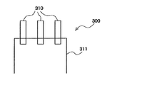
また、図6に示すように、ピエゾ内蔵型カンチレバーとして、アレイ構造のものを用いるのも有効である。ここでは、アレイ構造の電位検出装置300として、ピエゾ内蔵型カンチレバー310を3つ並べてアレイ構造とした構成を採用している。
As shown in FIG. 6, it is also effective to use an array structure as a piezo built-in cantilever. Here, as the
このようなアレイ構造とすることで、使用中にカンチレバーの破損、性能劣化が発生した際にも、他のカンチレバーを使用することで、継続して感光体の表面電位をモニターし続けることができる。アレイを構成するカンチレバーの数は、当然、多い方が破損等のリスク許容度が大きくなる。一方、カンチレバーの製造コストを抑える観点から3〜10本程度のカンチレバーで構成するのが好適である。 By using such an array structure, even when the cantilever is damaged or the performance is deteriorated during use, the surface potential of the photoconductor can be continuously monitored by using another cantilever. . As a matter of course, the larger the number of cantilevers constituting the array, the greater the risk tolerance such as breakage. On the other hand, from the viewpoint of reducing the manufacturing cost of the cantilever, it is preferable that the cantilever is composed of about 3 to 10 cantilevers.
次に、本実施形態の電位検出装置10について図7及び図8を参照して具体的に説明する。本発明の発明者は、検知対象の部材と距離が異なる2つの位置にピエゾ内蔵型カンチレバーを配置することが有効であることを知見した。
Next, the
感光体等の検知の対象部材は、装置が動作中は回転や移動しているため、常に、振れが発生する。ピエゾ内蔵型カンチレバーで検知する鏡像力検出は、対象部材との距離に依存するため、振れによって距離変動が発生すると、検出する鏡像力と、鏡像力から算出する電位値も変動することになる。例えば、感光体であれば、10〜50μm程度の振れは発生するが、この距離の変動が鏡像力の検出値に直接に影響することになる。ここで、感光体等の対象部材上の電荷により、ピエゾ内蔵型のカンチレバーに反対極性の電荷が誘起され、対象部材とピエゾ内蔵型のカンチレバーとの間に作用するクーロン力が生じる。このクーロン力が鏡像力のことであり、対象部材上の電荷の量によりクーロン力が変化する。このクーロン力の作用により、ピエゾ内蔵型のカンチレバーは対象部材側へ引っ張られるように変形する。この変形が、たわみ量や反り量として検知される。 Since the detection target member such as the photosensitive member rotates or moves during operation of the apparatus, the shake always occurs. The image force detection detected by the piezo built-in cantilever depends on the distance from the target member. Therefore, when a variation in distance occurs due to a shake, the detected image force and the potential value calculated from the image force also vary. For example, in the case of a photoconductor, a shake of about 10 to 50 μm occurs, but this variation in distance directly affects the detected value of the image force. Here, the charge on the target member such as the photosensitive member induces a charge of opposite polarity to the cantilever with built-in piezo, and a Coulomb force acting between the target member and the cantilever with built-in piezo is generated. This Coulomb force is a mirror image force, and the Coulomb force changes depending on the amount of charge on the target member. Due to the action of the Coulomb force, the piezoelectric built-in cantilever is deformed so as to be pulled toward the target member. This deformation is detected as a deflection amount or a warp amount.
そこで、本実施形態の電位検出装置10は、図7に示すように、検知の対象部材としての感光体20に対して略垂直方向にそれぞれ異なる距離を空けて、位置1と位置2とに2つのピエゾ内蔵型カンチレバーを配置している。さらに、所定の保持部材14により2つのピエゾ内蔵型カンチレバーを相互に一定の距離を空けて保持している。なお、保持部材としては、2つのピエゾ内蔵型カンチレバーを相互に一定の距離を空けて保持できる構造であれば、図7に記載の構造に限定されない。また、2つのピエゾ内蔵型カンチレバーの固定方法としては、ネジ等の固定部材で固定してもよく、接着剤等により固定してもよい。
Therefore, as shown in FIG. 7, the
ここでは、例えば感光体20から約200μm空けてピエゾ12xを備えたカンチレバー11xが配置され、ピエゾ12yを備えたカンチレバー11yがピエゾ内蔵型カンチレバー11xとの間に一定の距離、約100μmを空けて配置されている。
Here, for example, a
このように、対象部材と距離の異なる2つの位置にカンチレバーを配置し、かつ、これらのカンチレバーを構成し、装置の動作中も、カンチレバー間の距離は変動しないように配置して鏡像力を検出することで上述の感光体の振れに対応することができる。いずれのカンチレバーとも、感光体20との距離は装置の動作中に変動し得るが、カンチレバー間の距離は常に100μmと固定である。
In this way, the cantilevers are arranged at two positions that are different from the target member, and these cantilevers are configured so that the distance between the cantilevers does not change even during operation of the device, and the mirror image force is detected. By doing so, it is possible to cope with the above-mentioned shake of the photosensitive member. In any of the cantilevers, the distance from the
本実施形態において、上述のようにカンチレバー間の距離を常に100μmと固定することにより得られる利点について、図8を参照して説明する。図8は、横軸に感光体20の表面からのカンチレバーの距離X[μm]をとり、縦軸にカンチレバーに働く鏡像力F[nN]をとって、両者の相関をみるグラフである。そして、感光体20の表面電位が100Vの場合に得られる数値を『◆』で示し、感光体20の表面電位が200Vの場合に得られる数値を『□』で示し、感光体20の表面電位が500Vの場合に得られる数値を『×』で示している。
In the present embodiment, the advantages obtained by always fixing the distance between the cantilevers to 100 μm as described above will be described with reference to FIG. FIG. 8 is a graph showing the correlation between the horizontal axis with the cantilever distance X [μm] from the surface of the
また、図8(a)は、感光体20に振れが全く発生しないとした理想的な状態を示したグラフであり、この場合は、各カンチレバー単体で感光体20の表面電位を検出することができる。一方、図8(b)は、感光体20に振れが発生して、カンチレバーと感光体20との間隔が上記の理想的な状態より狭くなった状態を示している。また、図8(c)は、感光体20に振れが発生して、カンチレバーと感光体20との間隔が上記の理想的な状態より広くなった状態を示している。
FIG. 8A is a graph showing an ideal state in which no vibration is generated in the
ここで、検出値である鏡像力Fに対して、感光体の表面電位V、感光体と感光体側のカンチレバーの距離Xとした場合、V=k×F/Xが成立する。なお、kは予め決定可能な比例定数である。Xは装置の動作中に変動するため未知数となり、カンチレバーと感光体間の距離が1水準の状態では、距離Xと感光体の表面電位Vの2つの未知数は求めることができない。 Here, with respect to the mirror image force F which is a detected value, when the surface potential V of the photoconductor and the distance X between the photoconductor and the cantilever on the photoconductor side, V = k × F / X is established. Note that k is a proportional constant that can be determined in advance. Since X varies during the operation of the apparatus, it becomes an unknown, and when the distance between the cantilever and the photoconductor is one level, the two unknowns of the distance X and the surface potential V of the photoconductor cannot be obtained.
一方、上記のように常に、感光体20との距離を2水準に変えて、さらにカンチレバー同士の距離を100μmと固定にし、鏡像力を検出できれば、V=k×F/X、V=k×F/(X+100)の2式から、2つの未知数VとXを求めることができる。つまり、2つのカンチレバーが感光体20に対しての距離を異ならせ、さらに、2つのカンチレバー間の距離を固定することで、2つの未知数を求めることができる。
On the other hand, if the distance from the
カンチレバー間の距離は、対象部材の変動よりも大きく、かつ、対象部材から離れている、例えば本実施形態では位置2のカンチレバー11yでも鏡像力が検知できるように設定することが望ましい。本実施形態の一例では、100μmとしたが、具体的には、距離50〜100μmに設定するのが好適である。
The distance between the cantilevers is preferably set so that the mirror image force can be detected even by the
[第2実施形態]
次に、本発明における第2実施形態の電位検出装置について図面を参照して説明する。なお、第1実施形態と重複する内容については説明を省略する。
[Second Embodiment]
Next, a potential detection device according to a second embodiment of the present invention will be described with reference to the drawings. In addition, description is abbreviate | omitted about the content which overlaps with 1st Embodiment.
まず、本実施形態と第1実施形態との違いについて説明する。第1実施形態の電位検出装置によれば、ピエゾ内蔵型カンチレバーを用い、正確に感光体表面の光疲労を検知する等により、より精度の良い画像濃度の制御を行うことが可能となる。 First, the difference between this embodiment and 1st Embodiment is demonstrated. According to the potential detection device of the first embodiment, it is possible to control the image density with higher accuracy by using a piezo built-in cantilever and accurately detecting light fatigue on the surface of the photoreceptor.
一方、電子写真方式の画像形成装置においては、地汚れやクリーニング不良等、微量かつ点在する異常トナーが発生するような不具合が見られる。クリーニング不良等を防ぐため、異常トナーを検出する必要があるが、トナー電荷によって発生する電位は感光体等の部材上の電位よりもさらに小さいため、これを解決する構成を第1実施形態に加える必要がある。そこで、本発明者は、電圧印加手段により、ピエゾ内蔵型カンチレバーに所定の電圧を印加することで電位検知精度を向上させて、トナーの有無を検出する本実施形態の構成を知見した。 On the other hand, in the electrophotographic image forming apparatus, there is a problem that a small amount of scattered abnormal toner is generated, such as scumming or defective cleaning. Abnormal toner needs to be detected in order to prevent poor cleaning and the like. However, since the potential generated by the toner charge is even smaller than the potential on the member such as the photoreceptor, a configuration for solving this is added to the first embodiment. There is a need. Therefore, the present inventor has found the configuration of the present embodiment in which the potential detection accuracy is improved by applying a predetermined voltage to the piezoelectric built-in cantilever by the voltage applying means to detect the presence or absence of toner.
さらに、本実施形態においては、印加する電圧を所定の交流電圧とし、カンチレバーへの最大印加電圧、つまりピークツーピーク電圧を上げて、電位検出精度を上げることとした。また、対象部材の線速に応じて電圧周波数を変える制御を行う。これにより、カンチレバー下をトナーが通過する際に、その交流周期が通過時間以下になるような、交流電圧をカンチレバーに印加するようにした。本実施形態によれば、カンチレバーに電圧を印加することで、電位計測時のカンチレバー変位が増幅されて、トナー電位レベルの微小電位が計測できるので、部材表面上のトナー電位とトナー存在の有無を正確に検出可能となり、画像形成装置が動作中の異常発生によるユーザー負荷を低減することが可能となる。ここで、ピークツーピーク電圧とは、交流電圧を印加した際の最大電圧と最小電圧の差分である。 Furthermore, in the present embodiment, the voltage to be applied is set to a predetermined AC voltage, and the maximum applied voltage to the cantilever, that is, the peak-to-peak voltage is increased to increase the potential detection accuracy. Moreover, control which changes a voltage frequency according to the linear velocity of an object member is performed. As a result, when the toner passes under the cantilever, an AC voltage is applied to the cantilever so that the AC cycle is equal to or shorter than the passing time. According to the present embodiment, by applying a voltage to the cantilever, the displacement of the cantilever at the time of potential measurement is amplified and a minute potential at the toner potential level can be measured. It becomes possible to detect accurately, and it is possible to reduce the user load due to the occurrence of an abnormality while the image forming apparatus is operating. Here, the peak-to-peak voltage is a difference between the maximum voltage and the minimum voltage when an AC voltage is applied.
なお、本実施形態においては、専らトナーを検知する実施態様について説明するが、本発明はこれに限定されず、対象部材の電位検出の精度を高めることが必要なシーンにおいて適用することができる。 In the present embodiment, an embodiment in which toner is exclusively detected will be described. However, the present invention is not limited to this, and can be applied to a scene where it is necessary to improve the accuracy of potential detection of a target member.
本実施形態の電位検出装置を備えた画像形成装置400の概略構成について図9を参照して説明する。図9に示すように、本実施形態においては、電位検出装置としての、ピエゾ内蔵型カンチレバーによるセンシング部410を、ブレード80の下流側に設置する。また、図3(b)で示すように、第1実施形態と同様に、感光体の長手方向に対して平行に隙間無くカンチレバーを設けることで、感光体の長手方向全域でのクリーニング不良を検知することができる。
A schematic configuration of an
ピエゾ内蔵型カンチレバーを用いての電位検出は、電圧印加により誘起されたカンチレバーの電荷と、感光体表面およびトナーの電荷との間に作用するクーロン力を、カンチレバーのたわみ、そり量として検出することによって行う。具体的には、ピエゾ内蔵型カンチレバー411には、電圧印加手段414により、ピークツーピーク電圧1〜500V、周波数1〜100kHzの交流電圧を印加し、ピーク電圧時点でのカンチレバーのたわみ、そり量を検出することで、電位を推定する。 The potential detection using the piezo built-in cantilever is to detect the Coulomb force acting between the charge of the cantilever induced by voltage application and the charge of the photoconductor surface and toner as the deflection and warpage amount of the cantilever. Do by. Specifically, an AC voltage having a peak-to-peak voltage of 1 to 500 V and a frequency of 1 to 100 kHz is applied to the piezoelectric built-in cantilever 411 by the voltage applying unit 414, and the deflection and warpage of the cantilever at the time of the peak voltage are measured. By detecting, the potential is estimated.
カンチレバー近傍に電荷が存在すれば、その鏡像力を検出することで、電位を検出することも可能だが、本実施形態のように、トナーのように微小の電位を検出する場合には、カンチレバーに電圧を印加して、カンチレバーの変形量を大きくすることが有効である。このように、交流電圧をピエゾ内蔵型カンチレバーに印加するのは、カンチレバーの変形量を大きくし、検出SN比を上げることである。この結果、感光体等の対象部材上の電荷によるものより大きな電荷がピエゾ内蔵型カンチレバーに存在することになり、対象部材上の電荷とピエゾ内蔵型カンチレバー上の電荷による鏡像力が増加する。 If there is an electric charge in the vicinity of the cantilever, it is possible to detect the potential by detecting its mirror image force. However, as in this embodiment, when detecting a very small potential like toner, the cantilever It is effective to increase the amount of deformation of the cantilever by applying a voltage. Thus, the application of the AC voltage to the piezoelectric built-in cantilever is to increase the amount of deformation of the cantilever and increase the detection SN ratio. As a result, a charge larger than that due to the charge on the target member such as the photoconductor is present in the piezoelectric built-in cantilever, and the image power due to the charge on the target member and the charge on the piezoelectric built-in cantilever increases.
カンチレバーに直流電圧を印加することによっても、検出するカンチレバーの変形量を増幅できる。しかし、交流電圧の方が、電圧印加によるカンチレバーへの負荷は小さいため、長期間、安定して電圧を印加し続けるためには、交流電圧を用いるのが良い。この場合、重要なのはカンチレバー変位のピークツーピーク信号なので、得られた変位信号にハイパスフィルターをかければよい。なお、交流電圧の方が直流電圧より電圧印加時の安定性が良いため、本実施形態では交流電圧を例示しているが、直流電圧であっても良いことは言うまでもない。 The amount of deformation of the cantilever to be detected can also be amplified by applying a DC voltage to the cantilever. However, since the AC voltage has a smaller load on the cantilever due to voltage application, it is better to use the AC voltage in order to keep applying the voltage stably for a long time. In this case, since the peak-to-peak signal of the cantilever displacement is important, it is sufficient to apply a high-pass filter to the obtained displacement signal. In addition, since alternating current voltage has better stability at the time of voltage application than direct current voltage, in this embodiment, although alternating current voltage is illustrated, it cannot be overemphasized that direct current voltage may be sufficient.
さらに、カンチレバーに印加する電圧、周波数のより具体的な値は、カンチレバー、感光体間のギャップ、感光体線速等で最適化すべきであるが、近年、画像形成装置に係る各部の高速化が進んでいるため、この点を反映させて周波数を設定しなければならない。 Furthermore, more specific values of the voltage and frequency applied to the cantilever should be optimized by the cantilever, the gap between the photoconductors, the linear velocity of the photoconductor, etc. In recent years, the speed of each part related to the image forming apparatus has been increased. Since this is advancing, the frequency must be set to reflect this point.
例えば、現状、製品化されている画像形成装置であれば、感光体線速は、100mm/sから1000mm/sである。線速1000mm/sで駆動している感光体上で、1ドットレベル程度、すなわち、約30um角の大きさのトナー層を検出するためには、30usecの時間幅で2、3周期の交流電圧を印加しなければならない。このため、周波数を約100kHzに設定する必要がある。 For example, if the image forming apparatus is currently commercialized, the photosensitive member linear velocity is 100 mm / s to 1000 mm / s. In order to detect a toner layer of about one dot level, that is, about 30 μm square on a photosensitive member driven at a linear speed of 1000 mm / s, an alternating voltage of two or three cycles with a time width of 30 usec. Must be applied. For this reason, it is necessary to set the frequency to about 100 kHz.
ここで、本実施形態のように2つのカンチレバーに電圧を印加する場合に、カンチレバー相互に作用する電界の影響を考慮した構成が必要である。これについて図10を参照して説明する。 Here, when a voltage is applied to two cantilevers as in the present embodiment, a configuration in consideration of the influence of an electric field acting on the cantilevers is necessary. This will be described with reference to FIG.
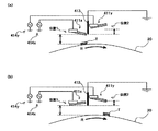
つまり、対象部材から距離の異なる2つのカンチレバー間で相互に電界が作用し、それぞれのカンチレバーの変形量が変わることにより検知精度に与える影響を考慮しなければならない。例えば、位置1のカンチレバー411xに印加した電圧により電界が発生し、その電界で位置2のカンチレバー411yが変形すると、感光体や感光体上のトナーの電位によるカンチレバーの変形量の検出精度が下がる。
That is, it is necessary to consider the influence on the detection accuracy due to the electric field acting between two cantilevers having different distances from the target member and the deformation amount of each cantilever changing. For example, when an electric field is generated by the voltage applied to the
そこで、図10に示すように2つのカンチレバーの間に、電界を遮断する電界遮断手段としてのシート413を配置することで、それぞれのカンチレバーから発生する電界を遮蔽する。これにより精度良く、感光体、およびトナーの電位を検出することが可能となる。なお、シート413は、導電性のある部材で構成し、かつ接地されている。例えば、Al(Aluminium)やSUS(Steel Use Stainless)の1mm厚のシートをカンチレバー間に配置することで、より精度の良い検出が可能となる。なお、図示の都合、第1実施形態では示した保持部材14を省略している。
Therefore, as shown in FIG. 10, by arranging a
ところで、上述のように、カンチレバー間にシート413を配置する場合、位置1のカンチレバー411x、2のカンチレバー411yそれぞれに同位相の交流電圧を印加すると、感光体20上の電位をモニタリングする位置は同じにはならない。
By the way, as described above, when the
そこで、本実施形態においては、図11に示すように、それぞれのカンチレバー間に印加する交流電圧の位相をずらした状態で、電位をセンシングする。これにより、図12に示すように、感光体20上の同一の位置、例えばトナーTをモニタリングすることが可能となる。矢印Rは、感光体20が回転する方向を示している。なお、具体的な位相のずれ量は、感光体線速と周方向のカンチレバーアレイ間の距離によって決定する。例えば、位相のずれ量は、感光体線速400mm/s、ピエゾ内蔵型のカンチレバーのアレイ間の距離1mmの場合、異なるカンチレバーアレイ間で同一の感光体の位置を検知する場合の時間差は2.5msecとなる。印加する交流電圧周波数が1kHz〔周期1msec〕とすれば、時間差2.5msecは、カンチレバー間で2.5周期の位相ずれに相当するので、カンチレバー間の位相差は180°に設定すれば良い。
Therefore, in this embodiment, as shown in FIG. 11, the potential is sensed in a state where the phase of the AC voltage applied between the cantilevers is shifted. As a result, as shown in FIG. 12, it is possible to monitor the same position on the
次に、図13(a)に示すように、例えば感光体20の長手方向に沿ってカンチレバーを複数並べたアレイ構造とした本実施形態の電位検出装置において、電位検出に与える影響を考慮する必要がある。その影響とは、本手法での検出ノイズ要因の1つに、感光体20の回転により発生する気流によってカンチレバーが変形することで、電位検出の際、ノイズを発生させるというものである。
Next, as shown in FIG. 13A, it is necessary to consider the influence on the potential detection in the potential detection device of this embodiment having an array structure in which a plurality of cantilevers are arranged along the longitudinal direction of the
そこで、本実施形態においては、図13(a)のZ部分を拡大表示した図13(b)のように、長手方向に連なるカンチレバーアレイで、隣り合うカンチレバーの支点を交互に反転して配置した。これにより、それぞれの信号の平均を求めることで、気流による検出ノイズを低減することが可能である。 Therefore, in the present embodiment, as shown in FIG. 13B in which the Z portion in FIG. 13A is enlarged and displayed, the fulcrum of adjacent cantilevers is alternately reversed and arranged in the cantilever array continuous in the longitudinal direction. . Thereby, it is possible to reduce the detection noise due to the airflow by obtaining the average of the respective signals.
感光体の近傍で発生する気流は、感光体の線速や、カンチレバー自体を含むセンシング部の配置、経時での回転振れ変動等で複雑に変化する。これに対して、図13(b)で示した配置とすれば、隣り合うカンチレバー間で、カンチレバーの支点とレバー自体が、感光体の回転方向に対して、対称になるように配置されているので、感光体の回転とカンチレバー自身を含むセンシング部の配置によって発生するランダムな気流の影響をキャンセルすることができる。 The airflow generated in the vicinity of the photoconductor varies in a complicated manner depending on the linear velocity of the photoconductor, the arrangement of the sensing unit including the cantilever itself, fluctuations in rotational shake with time, and the like. In contrast, with the arrangement shown in FIG. 13B, the cantilever fulcrum and the lever itself are arranged symmetrically with respect to the rotation direction of the photoconductor between adjacent cantilevers. Therefore, it is possible to cancel the influence of the random airflow generated by the rotation of the photoconductor and the arrangement of the sensing unit including the cantilever itself.
なお、上述する各実施の形態は、本発明の好適な実施の形態であり、本発明の要旨を逸脱しない範囲内において種々変更実施が可能である。例えば、本実施形態の電位検出装置10は、検知した電位ムラから露光量制御を行うことによる画像濃度補正に適用する以外に、ユーザーに感光体の交換メッセージを提示する際にも適用することができる。例えば、露光量で現像ポテンシャルを調整しきれない程、光疲労が極度に進行した場合は、感光体交換のメッセージをユーザーに知らせることで、スジ画像等の異常画像の発生を未然に防ぐことができる。
Each of the above-described embodiments is a preferred embodiment of the present invention, and various modifications can be made without departing from the scope of the present invention. For example, the
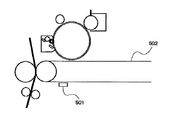
また、本実施形態の電位検出装置は、図14及び図15に示すように、他の電子写真部材の状態検知にも適用可能である。図14は、転写ベルト502の表面電位を検出するため電位検出装置501を設けた他の画像形成装置の構成であり、図15は、帯電ローラ603の表面電位を検出するために電位検出装置601を設けた他の画像形成装置の構成である。
Further, the potential detection apparatus of the present embodiment can be applied to state detection of other electrophotographic members as shown in FIGS. FIG. 14 shows the configuration of another image forming apparatus provided with a
このように、本実施形態の電位検出装置は、経時での表面汚染による、転写ベルトや帯電ローラの電位ムラ発生を検知することにも適用可能である。転写ベルトや帯電ローラの場合、放電を用いて、長手方向に一様に電位を印加するため、長手方向の電位を補正することはできないが、適切なタイミングでユーザーに、転写ベルトや帯電ローラの交換をするようにメッセージを提示することができる。また、転写ベルトや帯電ローラ上のトナーを検知してクリーニング不良等を防止することができる。 As described above, the potential detection apparatus of the present embodiment can also be applied to detect the occurrence of potential unevenness in the transfer belt and the charging roller due to surface contamination over time. In the case of a transfer belt or charging roller, the electric potential is uniformly applied in the longitudinal direction by using electric discharge. Therefore, the potential in the longitudinal direction cannot be corrected. A message can be presented to exchange. In addition, it is possible to detect a toner on the transfer belt or the charging roller to prevent a cleaning failure or the like.
1、400 画像形成装置
10、300、501、601 電位検出装置
11、310、411 カンチレバー
11a ピエゾ内蔵カンチレバー
12 ピエゾ(駆動機構)
13、14 保持部材
20 感光体
300 アレイユニット
502 中間転写ベルト
603 帯電ローラ
700 自己検知型SPMプローブ
DESCRIPTION OF SYMBOLS 1,400
13, 14
Claims (11)
前記対象部材に対して略垂直方向にそれぞれ異なる距離を空けて配置された少なくとも2つのピエゾ内蔵型カンチレバーと、
前記対象部材と前記ピエゾ内蔵型カンチレバーとの間に働く原子間力による前記ピエゾ内蔵型カンチレバーのたわみ量に基づいて前記対象部材の電位を測定する測定手段と、
前記少なくとも2つのピエゾ内蔵型カンチレバーを相互に一定の距離を空けて保持する保持手段とを備えることを特徴とする電位検出装置。 A potential detection device for detecting a potential of a target member,
At least two piezo built-in cantilevers arranged at different distances in a substantially vertical direction with respect to the target member;
Measuring means for measuring the potential of the target member based on the amount of deflection of the piezoelectric built-in cantilever due to an atomic force acting between the target member and the piezoelectric built-in cantilever;
A potential detecting device comprising: holding means for holding the at least two piezo-embedded cantilevers at a predetermined distance from each other.
Priority Applications (1)
| Application Number | Priority Date | Filing Date | Title |
|---|---|---|---|
| JP2013122037A JP6179205B2 (en) | 2013-02-25 | 2013-06-10 | Potential detection apparatus and image forming apparatus |
Applications Claiming Priority (3)
| Application Number | Priority Date | Filing Date | Title |
|---|---|---|---|
| JP2013034357 | 2013-02-25 | ||
| JP2013034357 | 2013-02-25 | ||
| JP2013122037A JP6179205B2 (en) | 2013-02-25 | 2013-06-10 | Potential detection apparatus and image forming apparatus |
Publications (2)
| Publication Number | Publication Date |
|---|---|
| JP2014186018A true JP2014186018A (en) | 2014-10-02 |
| JP6179205B2 JP6179205B2 (en) | 2017-08-16 |
Family
ID=51833704
Family Applications (1)
| Application Number | Title | Priority Date | Filing Date |
|---|---|---|---|
| JP2013122037A Expired - Fee Related JP6179205B2 (en) | 2013-02-25 | 2013-06-10 | Potential detection apparatus and image forming apparatus |
Country Status (1)
| Country | Link |
|---|---|
| JP (1) | JP6179205B2 (en) |
Citations (4)
| Publication number | Priority date | Publication date | Assignee | Title |
|---|---|---|---|---|
| US4205267A (en) * | 1977-11-03 | 1980-05-27 | Williams Bruce T | High speed electrostatic voltmeter |
| JPS60152959A (en) * | 1984-01-20 | 1985-08-12 | Nec Corp | Potential sensor |
| JPH05249165A (en) * | 1992-03-06 | 1993-09-28 | Omron Corp | Semiconductor potential sensor |
| JP2004239808A (en) * | 2003-02-07 | 2004-08-26 | Sony Corp | Surface potential sensor |
-
2013
- 2013-06-10 JP JP2013122037A patent/JP6179205B2/en not_active Expired - Fee Related
Patent Citations (4)
| Publication number | Priority date | Publication date | Assignee | Title |
|---|---|---|---|---|
| US4205267A (en) * | 1977-11-03 | 1980-05-27 | Williams Bruce T | High speed electrostatic voltmeter |
| JPS60152959A (en) * | 1984-01-20 | 1985-08-12 | Nec Corp | Potential sensor |
| JPH05249165A (en) * | 1992-03-06 | 1993-09-28 | Omron Corp | Semiconductor potential sensor |
| JP2004239808A (en) * | 2003-02-07 | 2004-08-26 | Sony Corp | Surface potential sensor |
Also Published As
| Publication number | Publication date |
|---|---|
| JP6179205B2 (en) | 2017-08-16 |
Similar Documents
| Publication | Publication Date | Title |
|---|---|---|
| US7715742B2 (en) | Photoconductor life through active control of charger settings | |
| JP4642486B2 (en) | Abnormality determination apparatus and image forming apparatus | |
| US8948620B2 (en) | Image forming system and latent image carrier replacement time detection method | |
| JP5246591B2 (en) | Image forming apparatus | |
| JP3361071B2 (en) | Automatic charging device cleaning method and image forming apparatus | |
| JP6179205B2 (en) | Potential detection apparatus and image forming apparatus | |
| JP2008107398A (en) | Remaining toner deposition amount detection method, transfer output control method, and image forming method and device | |
| JP6206536B2 (en) | Moving body displacement detection device, image forming apparatus, and moving body displacement detection method | |
| JP4478446B2 (en) | Image forming apparatus | |
| JP4642485B2 (en) | Abnormality judgment device | |
| JP2013117619A (en) | Image forming apparatus | |
| JP2012203178A (en) | Image forming apparatus | |
| JP4734465B2 (en) | Recording body abnormality occurrence prediction apparatus and image forming apparatus | |
| JP2007304184A (en) | Image forming apparatus and method for updating electrifying voltage for image forming apparatus | |
| JP4250075B2 (en) | Image forming apparatus | |
| JP2008233187A (en) | Speed change detection apparatus, image forming apparatus and speed change detection method | |
| KR101887650B1 (en) | Image forming apparatus and control method thereof | |
| JP2013109281A (en) | Image forming apparatus | |
| JP2011013240A (en) | Image forming apparatus | |
| JP5645545B2 (en) | Image forming apparatus | |
| JP5831804B2 (en) | Maintenance support system | |
| JP5157118B2 (en) | Image forming apparatus | |
| JP2005242179A (en) | Image forming device | |
| JP4522776B2 (en) | Belt device and image forming apparatus | |
| JP6337609B2 (en) | Flow velocity measuring apparatus and image forming apparatus |
Legal Events
| Date | Code | Title | Description |
|---|---|---|---|
| A621 | Written request for application examination |
Free format text: JAPANESE INTERMEDIATE CODE: A621 Effective date: 20160607 |
|
| RD01 | Notification of change of attorney |
Free format text: JAPANESE INTERMEDIATE CODE: A7421 Effective date: 20161216 |
|
| A977 | Report on retrieval |
Free format text: JAPANESE INTERMEDIATE CODE: A971007 Effective date: 20170217 |
|
| A131 | Notification of reasons for refusal |
Free format text: JAPANESE INTERMEDIATE CODE: A131 Effective date: 20170228 |
|
| A521 | Written amendment |
Free format text: JAPANESE INTERMEDIATE CODE: A523 Effective date: 20170427 |
|
| TRDD | Decision of grant or rejection written | ||
| A01 | Written decision to grant a patent or to grant a registration (utility model) |
Free format text: JAPANESE INTERMEDIATE CODE: A01 Effective date: 20170620 |
|
| A61 | First payment of annual fees (during grant procedure) |
Free format text: JAPANESE INTERMEDIATE CODE: A61 Effective date: 20170703 |
|
| R151 | Written notification of patent or utility model registration |
Ref document number: 6179205 Country of ref document: JP Free format text: JAPANESE INTERMEDIATE CODE: R151 |
|
| LAPS | Cancellation because of no payment of annual fees |