JP2014102500A - Liquid crystal display and method for manufacturing the same - Google Patents
Liquid crystal display and method for manufacturing the same Download PDFInfo
- Publication number
- JP2014102500A JP2014102500A JP2013222927A JP2013222927A JP2014102500A JP 2014102500 A JP2014102500 A JP 2014102500A JP 2013222927 A JP2013222927 A JP 2013222927A JP 2013222927 A JP2013222927 A JP 2013222927A JP 2014102500 A JP2014102500 A JP 2014102500A
- Authority
- JP
- Japan
- Prior art keywords
- liquid crystal
- film
- crystal display
- display device
- space layer
- Prior art date
- Legal status (The legal status is an assumption and is not a legal conclusion. Google has not performed a legal analysis and makes no representation as to the accuracy of the status listed.)
- Pending
Links
Images


Classifications
-
- G—PHYSICS
- G02—OPTICS
- G02F—OPTICAL DEVICES OR ARRANGEMENTS FOR THE CONTROL OF LIGHT BY MODIFICATION OF THE OPTICAL PROPERTIES OF THE MEDIA OF THE ELEMENTS INVOLVED THEREIN; NON-LINEAR OPTICS; FREQUENCY-CHANGING OF LIGHT; OPTICAL LOGIC ELEMENTS; OPTICAL ANALOGUE/DIGITAL CONVERTERS
- G02F1/00—Devices or arrangements for the control of the intensity, colour, phase, polarisation or direction of light arriving from an independent light source, e.g. switching, gating or modulating; Non-linear optics
- G02F1/01—Devices or arrangements for the control of the intensity, colour, phase, polarisation or direction of light arriving from an independent light source, e.g. switching, gating or modulating; Non-linear optics for the control of the intensity, phase, polarisation or colour
- G02F1/13—Devices or arrangements for the control of the intensity, colour, phase, polarisation or direction of light arriving from an independent light source, e.g. switching, gating or modulating; Non-linear optics for the control of the intensity, phase, polarisation or colour based on liquid crystals, e.g. single liquid crystal display cells
- G02F1/133—Constructional arrangements; Operation of liquid crystal cells; Circuit arrangements
- G02F1/1333—Constructional arrangements; Manufacturing methods
- G02F1/1341—Filling or closing of cells
-
- G—PHYSICS
- G02—OPTICS
- G02F—OPTICAL DEVICES OR ARRANGEMENTS FOR THE CONTROL OF LIGHT BY MODIFICATION OF THE OPTICAL PROPERTIES OF THE MEDIA OF THE ELEMENTS INVOLVED THEREIN; NON-LINEAR OPTICS; FREQUENCY-CHANGING OF LIGHT; OPTICAL LOGIC ELEMENTS; OPTICAL ANALOGUE/DIGITAL CONVERTERS
- G02F1/00—Devices or arrangements for the control of the intensity, colour, phase, polarisation or direction of light arriving from an independent light source, e.g. switching, gating or modulating; Non-linear optics
- G02F1/01—Devices or arrangements for the control of the intensity, colour, phase, polarisation or direction of light arriving from an independent light source, e.g. switching, gating or modulating; Non-linear optics for the control of the intensity, phase, polarisation or colour
- G02F1/13—Devices or arrangements for the control of the intensity, colour, phase, polarisation or direction of light arriving from an independent light source, e.g. switching, gating or modulating; Non-linear optics for the control of the intensity, phase, polarisation or colour based on liquid crystals, e.g. single liquid crystal display cells
- G02F1/133—Constructional arrangements; Operation of liquid crystal cells; Circuit arrangements
- G02F1/1333—Constructional arrangements; Manufacturing methods
- G02F1/133345—Insulating layers
-
- G—PHYSICS
- G02—OPTICS
- G02F—OPTICAL DEVICES OR ARRANGEMENTS FOR THE CONTROL OF LIGHT BY MODIFICATION OF THE OPTICAL PROPERTIES OF THE MEDIA OF THE ELEMENTS INVOLVED THEREIN; NON-LINEAR OPTICS; FREQUENCY-CHANGING OF LIGHT; OPTICAL LOGIC ELEMENTS; OPTICAL ANALOGUE/DIGITAL CONVERTERS
- G02F1/00—Devices or arrangements for the control of the intensity, colour, phase, polarisation or direction of light arriving from an independent light source, e.g. switching, gating or modulating; Non-linear optics
- G02F1/01—Devices or arrangements for the control of the intensity, colour, phase, polarisation or direction of light arriving from an independent light source, e.g. switching, gating or modulating; Non-linear optics for the control of the intensity, phase, polarisation or colour
- G02F1/13—Devices or arrangements for the control of the intensity, colour, phase, polarisation or direction of light arriving from an independent light source, e.g. switching, gating or modulating; Non-linear optics for the control of the intensity, phase, polarisation or colour based on liquid crystals, e.g. single liquid crystal display cells
- G02F1/133—Constructional arrangements; Operation of liquid crystal cells; Circuit arrangements
- G02F1/1333—Constructional arrangements; Manufacturing methods
- G02F1/1343—Electrodes
-
- G—PHYSICS
- G02—OPTICS
- G02F—OPTICAL DEVICES OR ARRANGEMENTS FOR THE CONTROL OF LIGHT BY MODIFICATION OF THE OPTICAL PROPERTIES OF THE MEDIA OF THE ELEMENTS INVOLVED THEREIN; NON-LINEAR OPTICS; FREQUENCY-CHANGING OF LIGHT; OPTICAL LOGIC ELEMENTS; OPTICAL ANALOGUE/DIGITAL CONVERTERS
- G02F1/00—Devices or arrangements for the control of the intensity, colour, phase, polarisation or direction of light arriving from an independent light source, e.g. switching, gating or modulating; Non-linear optics
- G02F1/01—Devices or arrangements for the control of the intensity, colour, phase, polarisation or direction of light arriving from an independent light source, e.g. switching, gating or modulating; Non-linear optics for the control of the intensity, phase, polarisation or colour
- G02F1/13—Devices or arrangements for the control of the intensity, colour, phase, polarisation or direction of light arriving from an independent light source, e.g. switching, gating or modulating; Non-linear optics for the control of the intensity, phase, polarisation or colour based on liquid crystals, e.g. single liquid crystal display cells
- G02F1/133—Constructional arrangements; Operation of liquid crystal cells; Circuit arrangements
- G02F1/136—Liquid crystal cells structurally associated with a semi-conducting layer or substrate, e.g. cells forming part of an integrated circuit
- G02F1/1362—Active matrix addressed cells
- G02F1/1368—Active matrix addressed cells in which the switching element is a three-electrode device
Abstract
Description
本発明は、液晶表示装置及びその製造方法に関する。 The present invention relates to a liquid crystal display device and a manufacturing method thereof.
液晶表示装置は、現在、最も幅広く使用されている平板表示装置の一つであって、画素電極と共通電極など電界生成電極が形成されている二枚の表示板と、その間に挿入されている液晶層とからなる。 The liquid crystal display device is one of the most widely used flat display devices at present, and is inserted between two display plates on which electric field generating electrodes such as a pixel electrode and a common electrode are formed. It consists of a liquid crystal layer.
電界生成電極に電圧を印加して液晶層に電界を生成し、これを通じて液晶層の液晶分子の配向を決定して、入射光の偏光を制御することによって画像を表示する。 A voltage is applied to the electric field generating electrode to generate an electric field in the liquid crystal layer, through which the orientation of the liquid crystal molecules in the liquid crystal layer is determined and the polarization of incident light is controlled to display an image.
NCD(Nano Crystal Display)液晶表示装置は、有機物質などで犠牲層を形成し、犠牲層の上に支持部材を形成した後に犠牲層を除去して、犠牲層の除去によって形成された空間に液晶を満たして製造する液晶表示装置である。 In an NCD (Nano Crystal Display) liquid crystal display device, a sacrificial layer is formed with an organic material, a support member is formed on the sacrificial layer, the sacrificial layer is removed, and a liquid crystal is formed in the space formed by removing the sacrificial layer. It is a liquid crystal display device manufactured by satisfying the above.
NCD(Nano Crystal Display)液晶表示装置の製造方法は、液晶分子を整列、配向するために、液晶を注入する段階以前に配向液を注入した後、乾燥させる工程を含む。配向液を乾燥する過程において、配向液中の微細固形分(粉)が固まり(coalesce)、大きい塊の群を形成する現象が発生して、光漏れ現象、透過率の低下現象、又は液晶物質を注入する後続工程を妨げるなどの問題が発生する。 A method of manufacturing an NCD (Nano Crystal Display) liquid crystal display device includes a step of injecting an alignment liquid before the step of injecting a liquid crystal and then drying it in order to align and align liquid crystal molecules. In the process of drying the alignment liquid, a phenomenon occurs in which fine solids (powder) in the alignment liquid are coalesced to form a large lump group, and light leakage phenomenon, transmittance decrease phenomenon, or liquid crystal substance Problems such as hindering the subsequent process of injecting.
本発明の目的は、配向物質及び液晶物質を円滑に注入できる液晶表示装置及びその製造方法を提供することにある。 An object of the present invention is to provide a liquid crystal display device capable of smoothly injecting an alignment material and a liquid crystal material, and a method for manufacturing the same.
本発明の一実施形態による液晶表示装置は、基板と、前記基板上に配置する薄膜トランジスタと、前記薄膜トランジスタの一端子と接続する画素電極と、前記画素電極上に配置して、液晶注入口を含み、画素領域に対応する複数の領域を含む微細空間層と、前記微細空間層上に配置する支持部材と、前記支持部材上に配置する第1疎水性膜と、前記支持部材上に配置して、前記液晶注入口を覆うキャッピング膜とを含む。 A liquid crystal display according to an embodiment of the present invention includes a substrate, a thin film transistor disposed on the substrate, a pixel electrode connected to one terminal of the thin film transistor, and a liquid crystal injection port disposed on the pixel electrode. A fine space layer including a plurality of regions corresponding to the pixel region, a support member disposed on the fine space layer, a first hydrophobic film disposed on the support member, and disposed on the support member. And a capping film covering the liquid crystal injection port.
前記複数の領域に形成された微細空間層のうち、互いに隣接する微細空間層の間に配置する第2疎水性膜をさらに含むことができる。
前記微細空間層の複数の領域の間にグルーブが形成され、前記キャッピング膜は前記グルーブを覆ってもよい。
前記グルーブで前記第2疎水性膜と前記キャッピング膜が接触してもよい。
前記第1疎水性膜は、前記支持部材の上部面に位置する第1部分と、前記第1部分から延在して前記グルーブ内の側面に沿って位置する第2部分とを含んでもよい。
前記基板上に配置する有機膜と、前記有機膜の間に配置する遮光部材とをさらに含み、前記第2疎水性膜は前記遮光部材と重なってもよい。
前記微細空間層上に配置する共通電極をさらに含んでもよい。
前記微細空間層を取り囲む前記画素電極の表面及び前記共通電極の表面に親水性処理を施してもよい。
前記画素電極と前記微細空間層又は前記共通電極と前記微細空間層の間に配置する配向膜をさらに含んでもよい。
前記微細空間層は液晶物質を含んでもよい。
前記第1疎水性膜は、炭素、水素又はフッ素を含んでもよい。
A second hydrophobic layer may be further disposed between the adjacent minute space layers among the minute space layers formed in the plurality of regions.
A groove may be formed between a plurality of regions of the fine space layer, and the capping film may cover the groove.
The second hydrophobic film and the capping film may be in contact with each other in the groove.
The first hydrophobic membrane may include a first portion located on an upper surface of the support member and a second portion extending from the first portion and located along a side surface in the groove.
An organic film disposed on the substrate and a light shielding member disposed between the organic films may be further included, and the second hydrophobic film may overlap the light shielding member.
A common electrode disposed on the fine space layer may be further included.
A hydrophilic treatment may be applied to the surface of the pixel electrode surrounding the fine space layer and the surface of the common electrode.
An alignment film disposed between the pixel electrode and the fine space layer or between the common electrode and the fine space layer may be further included.
The fine space layer may include a liquid crystal material.
The first hydrophobic film may include carbon, hydrogen, or fluorine.
本発明の一実施形態による液晶表示装置の製造方法は、基板上に薄膜トランジスタを形成する段階と、前記薄膜トランジスタ上に画素電極を形成する段階と、前記画素電極上に犠牲膜を形成する段階と、前記犠牲膜上に支持部材を形成する段階と、前記犠牲膜を除去して液晶注入口を含む微細空間層を形成する段階と、前記支持部材上に第1疎水性膜を形成する段階と、前記微細空間層に液晶物質を注入する段階と、前記支持部材上に前記液晶注入口を覆うようにキャッピング膜を形成する段階とを含む。 A method of manufacturing a liquid crystal display according to an embodiment of the present invention includes: forming a thin film transistor on a substrate; forming a pixel electrode on the thin film transistor; forming a sacrificial film on the pixel electrode; Forming a support member on the sacrificial film; removing the sacrificial film to form a fine space layer including a liquid crystal inlet; and forming a first hydrophobic film on the support member; Injecting a liquid crystal material into the fine space layer and forming a capping film on the support member so as to cover the liquid crystal injection port.
前記微細空間層は、画素領域に対応する複数の領域を含み、前記複数の領域に形成された微細空間層のうち、互いに隣接する微細空間層の間に位置する第2疎水性膜を形成する段階をさらに含んでもよい。
前記微細空間層の複数の領域の間にグルーブを形成し、前記キャッピング膜は前記グルーブを覆うように形成してもよい。
前記グルーブで前記第2疎水性膜と前記キャッピング膜が接触するように形成してもよい。
前記第1疎水性膜は、前記支持部材の上部面に上に位置する第1部分と、前記第1部分から延在して前記グルーブ内の側面を覆うように位置する第2部分とを含むように形成してもよい。
前記基板上に有機膜を形成する段階と、前記有機膜の間に遮光部材を形成する段階とをさらに含み、前記第2疎水性膜は前記遮光部材と重なるように形成してもよい。
前記犠牲膜上に共通電極を形成する段階をさらに含んでもよい。
前記微細空間層を取り囲む前記画素電極の表面及び前記共通電極の表面に親水性処理を施す段階をさらに含んでもよい。
前記親水性処理の段階は、酸素を含むプラズマ処理を施す段階をさらに含んでもよい。
The fine space layer includes a plurality of regions corresponding to the pixel region, and forms a second hydrophobic film positioned between the minute space layers adjacent to each other among the fine space layers formed in the plurality of regions. A step may further be included.
A groove may be formed between a plurality of regions of the fine space layer, and the capping film may be formed to cover the groove.
The groove may be formed so that the second hydrophobic film and the capping film are in contact with each other.
The first hydrophobic membrane includes a first portion located on an upper surface of the support member, and a second portion extending from the first portion and located to cover a side surface in the groove. You may form as follows.
The method may further include forming an organic film on the substrate and forming a light shielding member between the organic films, and the second hydrophobic film may be formed to overlap the light shielding member.
The method may further include forming a common electrode on the sacrificial film.
The method may further include performing a hydrophilic treatment on the surface of the pixel electrode surrounding the fine space layer and the surface of the common electrode.
The hydrophilic treatment may further include performing a plasma treatment including oxygen.
本発明の一実施形態によれば、親水性処理又は疎水性処理を施すことにより、配向物質及び液晶の注入を円滑に行うことができる。 According to one embodiment of the present invention, the alignment material and the liquid crystal can be smoothly injected by performing the hydrophilic treatment or the hydrophobic treatment.
以下、添付した図面を参照して、本発明の好ましい実施形態について詳細に説明する。しかし、本発明はここで説明される実施形態に限定されず、他の形態に具体化できる。むしろ、ここで紹介される実施形態は、開示された内容を徹底的、且つ完全にし、そして当業者に本発明の思想を十分に伝達するために提供される。 Hereinafter, exemplary embodiments of the present invention will be described in detail with reference to the accompanying drawings. However, the present invention is not limited to the embodiments described herein, and can be embodied in other forms. Rather, the embodiments introduced herein are provided so that this disclosure will be thorough and complete, and will fully convey the spirit of the invention to those skilled in the art.
図面において、層及び領域の厚さは、明確性を期するために誇張されて示した。また、或る層が他の層又は基板「上」にあると言及される場合に、それは他の層又は基板上に直接形成されるか、又はそれらの間に第3の層が介される。明細書の全体にわたって同一の参照番号で表示された部分は、同一の構成要素を意味する。 In the drawings, the thickness of layers and regions are exaggerated for clarity. Also, when a layer is referred to as being “on” another layer or substrate, it is formed directly on the other layer or substrate, or a third layer interposed therebetween. Parts denoted by the same reference numerals throughout the specification refer to the same components.
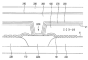
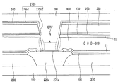
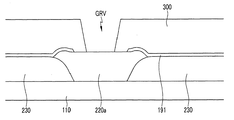
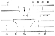
図1は、本発明の一実施形態による液晶表示装置を示す平面図である。図2は、図1の切断線II−IIに沿った断面図である。図3は、図1の切断線III−IIIに沿った断面図である。図4は、図1乃至図3の実施形態による微細空間層を示す斜視図である。 FIG. 1 is a plan view showing a liquid crystal display device according to an embodiment of the present invention. FIG. 2 is a cross-sectional view taken along a cutting line II-II in FIG. FIG. 3 is a cross-sectional view taken along section line III-III in FIG. FIG. 4 is a perspective view illustrating a fine space layer according to the embodiment of FIGS. 1 to 3.
図1乃至図3を参照すれば、透明なガラス又はプラスチックなどからなる基板110の上に薄膜トランジスタQa、Qb、Qcを配置する。
薄膜トランジスタQa、Qb、Qcが形成されている基板110の上に有機膜230の複数の部分(portion)を配置し、有機膜230の隣接する部分の間に遮光部材220を形成する。
有機膜230の各部分の上に画素電極191を配置し、画素電極191は、コンタクトホール185a、185bによって薄膜トランジスタQa、Qbの一端子と電気的に接続される。
Referring to FIGS. 1 to 3, thin film transistors Qa, Qb, and Qc are disposed on a
A plurality of portions of the
A
図2及び図3は、切断線II−IIと切断線III−IIIに沿った断面図であるが、図2及び図3においては図1に示した基板110と有機膜230の間の構成を省略した。実際には上述のように、図2及び図3で基板110と有機膜230の間に薄膜トランジスタQa、Qb、Qcの構成の一部を含む。
2 and 3 are cross-sectional views along the cutting line II-II and the cutting line III-III. In FIGS. 2 and 3, the configuration between the
有機膜230は、画素電極191の列方向に沿って長く延在し得る。有機膜230はカラーフィルタの役割を果たすことができ、その場合、有機膜(カラーフィルタ)230は、赤色、緑色、及び青色の三原色などの原色(primary color)のうちの一つを表示する。しかし、赤色、緑色、及び青色の三原色に制限されず、青緑色(cyan)、紫紅色(magenta)、イエロー(yellow)、及びホワイト系の色のうちの一つを表示する場合もある。
The
互いに隣接する有機膜230の部分は、図1において、各々タイル状をなし、横方向D及びこれと交差する縦方向に沿って離隔する。図2では横方向Dに沿って互いに離隔している有機膜230を示し、図3では縦方向に沿って互いに離隔している有機膜230を示す。
The portions of the
図2を参照すれば、横方向Dに沿って離隔している有機膜230の部分の間に縦遮光部材220bが位置する。図3を参照すれば、縦方向に沿って離隔している有機膜230の間には横遮光部材220aが位置する。縦遮光部材220bの周縁は、隣接する有機膜230の部分の各々の周縁と重なっており、縦遮光部材220bが有機膜230の両側周縁と重なる幅は実質的に同一であり得る。横遮光部材220aの周縁は、隣接する有機膜230の部分の各々の周縁と重なっており、横遮光部材220aが有機膜230の両側周縁と重なる幅は実質的に同一であり得る。
Referring to FIG. 2, the vertical
画素電極191の上には下部配向膜11が形成されており、下部配向膜11は例えば、垂直配向膜である。下部配向膜11は、ポリアミド酸(Polyamic acid)、ポリシロキサン(Polysiloxane)又はポリイミド(Polyimide)などの液晶配向膜であって、一般に使用される物質のうちの少なくとも一つを含んで形成できる。
A
下部配向膜11の上には微細空間層400を配置する。微細空間層400には液晶分子310を含む液晶物質が注入されており、微細空間層400は液晶注入口Aを有する。微細空間層400は、画素電極191の列方向、つまり縦方向に沿って形成される。本実施形態において、下部、上部配向膜11、21を形成する配向物質と、液晶分子310を含む液晶物質とは、毛管力(capillary force)を利用して微細空間層400に注入される。
A
図3をさらに参照すれば、本実施形態では隣接する微細空間層400の間であって、例えば横遮光部材220aの上に第2疎水性膜275aが形成されている。第1疎水性膜275aは、炭素、水素又はフッ素を含み得る。第2疎水性膜275aは、液晶注入口Aを通じて液晶物質を注入するとき、液晶物質が分散せずに、液晶物質に含まれている液晶分子310の元の形状を維持するようにする。
Referring further to FIG. 3, in the present embodiment, a second
微細空間層400の上に上部配向膜21を配置し、上部配向膜21の上に共通電極270及び蓋膜250を配置する。共通電極270は共通電圧の印加を受け、データ電圧が印加された画素電極191と共に電界を生成して、二つの電極の間の微細空間層200に位置する液晶分子310が傾く方向を決定する。共通電極270は、画素電極191とキャパシタを構成して、薄膜トランジスタがターンオフ(turn−off)された後にも印加された電圧を維持する。蓋膜250は例えば、窒化ケイ素(SiNx)又は酸化ケイ素(SiO2)から形成される。
The
蓋膜250の上に支持部材(supporting member)260を配置する。支持部材260は、シリコンオキシカーバイド(SiOC)、フォトレジスト、又はその他の有機物質を含み得る。支持部材260がシリコンオキシカーバイド(SiOC)を含む場合には、化学気相蒸着法によって形成でき、フォトレジストを含む場合には、コーティング法によって形成できる。シリコンオキシカーバイド(SiOC)は、化学気相蒸着法によって形成できる膜のうち透過率が高く、膜のストレスも少なくので変形が生じない長所がある。従って、本実施形態で支持部材260をシリコンオキシカーバイド(SiOC)から形成することにより、光がよく透過し、膜ストレスが少なく、且つ安定的な膜を形成できる。
A supporting
横遮光部材220aの上には、微細空間層400、上部配向膜21、共通電極270、蓋膜250、及び支持部材260を貫くグルーブ(溝)GRVが形成されている。
以下、図2乃至図4を参照して、微細空間層400について具体的に説明する。
A groove (groove) GRV penetrating the
Hereinafter, the
図2乃至図4を参照すれば、微細空間層400は、ゲート線121aと重なる部分に位置する複数のグルーブGRVによって分割された、ゲート線121aが延在している方向Dに沿う複数の領域を含む。微細空間層400の複数の領域(region)は各々、複数の画素領域に対応する。
Referring to FIGS. 2 to 4, the
縦方向に沿って形成された微細空間層400の複数の領域を一つの集団というとき、その集団は行方向に複数形成されている。このとき、微細空間層400の間に形成されたグルーブGRVは、ゲート線121aが延在している方向Dに沿って配置され、微細空間層400の液晶注入口AはグルーブGRVと微細空間層400の境界部分に対応する領域を形成する。
When a plurality of regions of the
液晶注入口Aは、グルーブGRVが延在している方向に沿って形成されている。そして、ゲート線121aが延在している方向Dにおいて互いに隣接する微細空間層400の間に形成されたオープン部OPNは、図2に示したように支持部材260によって覆われ、埋められる。
The liquid crystal injection port A is formed along the direction in which the groove GRV extends. The open part OPN formed between the minute space layers 400 adjacent to each other in the direction D in which the
微細空間層400に含まれている液晶注入口Aは、上部配向膜21のグルーブGRVに面する端部と横遮光部材220aの間、即ち、上部配向膜21のグルーブGRVに面する端部と下部配向膜11のグルーブGRVに面する端部との間に配置される。
The liquid crystal injection hole A included in the
本実施形態において、グルーブGRVが、ゲート線121aが延在している方向Dに沿って形成されている場合を説明したが、他の実施形態では、グルーブGRVは、データ線171が延在している方向に沿って形成され、複数の領域を含む微細空間層400の集団が列方向に複数形成される。その場合、液晶注入口Aは、データ線171が延在している方向に沿って形成されたグルーブGRVが延在している方向に沿って形成される。
In this embodiment, the case where the groove GRV is formed along the direction D in which the
支持部材260の上に保護膜240を配置する。保護膜240は例えば、窒化ケイ素(SiNx)又は酸化ケイ素(SiO2)から形成される。保護膜240の上に第1疎水性膜275bを配置する。第1疎水性膜275bは、支持部材260の上部面に位置する第1部分275b1と、第1部分275b1から延在してグルーブGRV内の側面に沿って位置する第2部分275b2とを含む。
A
第1疎水性膜275bは例えば、炭素、水素又はフッ素を含む。グルーブGRVに液晶物質を滴下することによって液晶注入口Aを通じて液晶物質を微細空間層400内に注入しようとするとき、所望の位置に液晶物質が滴下されずにミスアライン(mis−align)が発生する恐れがある。即ち、このとき、グルーブGRVに近く位置する支持部材260又は保護膜240の上部面に液晶物質が滴下する。
このような場合、第1疎水性膜275bは、液晶物質に含まれている液晶分子310の元の形状を維持しながら、液晶物質が他のところに分散せずに、液晶注入口Aに向かって移動するように誘導する。
第1疎水性膜275bは、支持部材260の上部面の上に全面的に形成する必要はないので、他の実施形態では、液晶注入口Aが形成されているグルーブGRVに隣接して位置する支持部材260の上部面の上のみに形成する。
The first
In such a case, the first
Since the first
第1疎水性膜275bの上にキャッピング膜280を配置する。キャッピング膜280は、第1疎水性膜275bの第1部分275b1と第2部分275b2、及びグルーブGRVによって露出した微細空間層400の液晶注入口Aを覆う。キャッピング膜280は例えば、熱硬化性樹脂、シリコンオキシカーバイド(SiOC)又はグラフェン(Graphene)から形成される。
A
キャッピング膜280をグラフェンから形成する場合に、グラフェンはヘリウムなどを含むガスに対する不透過性(impermeability)が強い特性を有するので、液晶注入口Aを覆うキャッピング膜の役割を果たし、炭素結合からなる物質であるので、液晶物質と接触しても液晶物を汚染しない。それだけでなく、グラフェンは外部の酸素及び水分に対して液晶物質を保護する役割も果たす。
When the
本実施形態において、微細空間層400の液晶注入口Aを通じて液晶物質を注入するので、別途の上部基板を形成することなく、液晶表示装置を形成できる。
他の実施形態では、キャッピング膜280の上に無機膜又は有機膜から形成されたオーバーコート膜(図示せず)を配置する。オーバーコート膜は、外部衝撃から微細空間層400に注入された液晶分子310を保護し、膜を平坦化する役割を果たす。
In the present embodiment, since the liquid crystal material is injected through the liquid crystal injection port A of the
In another embodiment, an overcoat film (not shown) formed from an inorganic film or an organic film is disposed on the
以下、図1乃至図3をさらに参照して、本実施形態による液晶表示装置について詳細に説明する。
図1乃至図3を参照すれば、透明なガラス又はプラスチックなどからなる基板110の上に複数のゲート線121a、複数の減圧ゲート線121b、及び複数の維持電極線131を含む複数のゲート導電体が形成されている。
Hereinafter, the liquid crystal display device according to the present embodiment will be described in detail with reference to FIGS.
1 to 3, a plurality of gate conductors including a plurality of
ゲート線121a及び減圧(set−down)ゲート線121bは主に横方向に延在して、ゲート信号を伝達する。ゲート線121aは、図で上、下方に突出した第1ゲート電極124a及び第2ゲート電極124bを含み、減圧ゲート線121bは図で上方に突出した第3ゲート電極124cを含む。第1ゲート電極124a及び第2ゲート電極124bは、互いに接続されて一つの突出部を形成する。
The
維持電極線131も主に横方向に延在して、共通電圧Vcomなどの予め定められた電圧を伝達する。維持電極線131は上下に突出した維持電極129、ゲート線121aと実質的に垂直に延在した一対の縦部134、及び一対の縦部134の端を互いに接続する横部127を含む。横部127は下に拡張された容量電極137を含む。
The
ゲート線121a、減圧ゲート線121b、維持電極線131を含むゲート導電体の上にはゲート絶縁膜(図示せず)が形成されている。
ゲート絶縁膜の上には非晶質又は結晶質ケイ素などからなる複数の線状半導体(図示せず)が形成されている。線状半導体は、主に縦方向に延在して、第1ゲート電極124a及び第2ゲート電極124bに向かって延在しており、互いに接続されている第1半導体154a及び第2半導体154b、そして第3ゲート電極124cの上に位置する第3半導体154cを含む。
A gate insulating film (not shown) is formed on the gate conductor including the
A plurality of linear semiconductors (not shown) made of amorphous or crystalline silicon are formed on the gate insulating film. The linear semiconductor mainly extends in the vertical direction and extends toward the
半導体154a、154b、154cの上には各々、一対のオーミックコンタクト部材(図示せず)が形成される。オーミックコンタクト部材は、シリサイド(silicide)又はn型不純物が高濃度にドーピングされているn+水素化非晶質シリコンなどの物質で形成される。
A pair of ohmic contact members (not shown) are formed on the
オーミックコンタクト部材の上には複数のデータ線171、複数の第1ドレイン電極175a、複数の第2ドレイン電極175b、及び複数の第3ドレイン電極175cを含むデータ導電体が形成されている。
A data conductor including a plurality of
データ線171は、データ信号を伝達し、主に縦方向に延在してゲート線121a及び減圧ゲート線121bと交差する。各データ線171は、第1ゲート電極124a及び第2ゲート電極124bに向かって延在して互いに接続されている第1ソース電極173a及び第2ソース電極173bを含む。
The
第1ドレイン電極175a、第2ドレイン電極175b、及び第3ドレイン電極175cは、広い一端部と、棒状の他端部とを含む。第1ドレイン電極175a及び第2ドレイン電極175bの棒状の端部は、第1ソース電極173a及び第2ソース電極173bによって一部が取り囲まれている。第1ドレイン電極175aの広い一端部は、さらに延長されて「U」字状に曲がった第3ソース電極173cを形成する。第3ドレイン電極175cの広い端部177cは、容量電極137と重なって減圧キャパシタCstdを形成し、棒状端部は第3ソース電極173cによって一部が取り囲まれている。
The
第1ゲート電極124a、第1ソース電極173a、及び第1ドレイン電極175aは、第1半導体154aと共に第1薄膜トランジスタQaを形成し、第2ゲート電極124b、第2ソース電極173b、及び第2ドレイン電極175bは、第2半導体154bと共に第2薄膜トランジスタQbを形成し、第3ゲート電極124c、第3ソース電極173c、及び第3ドレイン電極175cは、第3半導体154cと共に第3薄膜トランジスタQcを形成する。
The
第1半導体154a、第2半導体154b、及び第3半導体154cを含む線状半導体は、ソース電極173a、173b、173cとドレイン電極175a、175b、175cの間のチャネル領域を除いては、データ導電体171、173a、173b、173c、175a、175b、175c及びその下部のオーミックコンタクト部材と実質的に同一の平面形状を有し得る。
The linear semiconductor including the
第1半導体154aには、第1ソース電極173aと第1ドレイン電極175aの間で第1ソース電極173a及び第1ドレイン電極175aによって覆われずに露出した部分があり、第2半導体154bには、第2ソース電極173bと第2ドレイン電極175bの間で第2ソース電極173b及び第2ドレイン電極175bによって覆われずに露出した部分があり、第3半導体154cには、第3ソース電極173cと第3ドレイン電極175cの間で第3ソース電極173c及び第3ドレイン電極175cによって覆われずに露出した部分がある。
The
データ導電体171、173a、173b、173c、175a、175b、175c及び上記露出した半導体154a、154b、154c部分の上には、窒化ケイ素又は酸化ケイ素などの無機絶縁物からなる下部保護膜(図示せず)が形成されている。
On the
下部保護膜の上にはカラーフィルタ230が配置され得る。カラーフィルタ230は、第1薄膜トランジスタQa、第2薄膜トランジスタQb、及び第3薄膜トランジスタQcなど位置する所を除いた大部分の領域に位置する。しかし、隣接するデータ線171の間に沿って縦方向に長く延在し得る。本実施形態において、カラーフィルタ230は画素電極191の下に形成されているが、共通電極270の上に形成し得る。
A
カラーフィルタ230が位置しない領域及びカラーフィルタ230の一部(端部)の上には遮光部材220を配置する。遮光部材220は、ゲート線121a及び減圧ゲート線121bに沿って延在して上下に拡張されており、第1薄膜トランジスタQa、第2薄膜トランジスタQb、及び第3薄膜トランジスタQcなどが位置する領域を覆う第1遮光部材220aとデータ線171に沿って延在している第2遮光部材220bを含む。
The
遮光部材220は、ブラックマトリックス(black matrix)ともいい、光漏れを防止する。
下部保護膜、遮光部材220には、第1ドレイン電極175a及び第2ドレイン電極175bを露出する複数のコンタクトホール185a、185bが形成されている。
The
A plurality of
そして、カラーフィルタ230、遮光部材220の上には第1副画素電極191a及び第2副画素電極191bを含む画素電極191が形成されている。第1副画素電極191aと第2副画素電極191bは、ゲート線121a及び減圧ゲート線121bを介して互いに分離され、各々上と下に配置されて列方向に隣接する。第2副画素電極191bの高さは、第1副画素電極191aの高さより高く、ほぼ1倍乃至3倍である。
A
第1副画素電極191a及び第2副画素電極191b各々の全体的な形状は四角形であり、第1副画素電極191a及び第2副画素電極191b各々は、横幹部193a、193b、及び横幹部193a、193bと交差する縦幹部192a、192bからなる十字状幹部を含む。また、第1副画素電極191a及び第2副画素電極191bは、各々複数の微細枝部194a、194b、下端の突出部197a、及び上端の突出部197bを含む。
The overall shape of each of the
画素電極191は、横幹部193a、193bと縦幹部192a、192bによって4個の副領域に分けられる。微細部194a、194bは、横幹部193a、193b及び縦幹部192a、192bから傾斜して延在しており、その延在する方向はゲート線121a、121b又は横幹部193a、193bとほぼ45度又は135度の角をなす。また、隣接する二つの副領域の微細部194a、194bが延在している方向は互いに直交する。
The
本実施形態において、第1副画素電極191aは、外郭を取り囲む外郭幹部をさらに含み、第2副画素電極191bは、上端及び下端に位置する横部、及び第1副画素電極191aの左右に位置する左右縦部をさらに含む。左右縦部は、データ線171と第1副画素電極191aの間の容量性結合、つまり、カップリングを防止する。
In the present embodiment, the
画素電極191の上には、下部配向膜11、微細空間層400、上部配向膜21、共通電極270、蓋膜250、及びキャッピング膜280などが形成されており、このような構成要素に対しては上述したので省略する。
On the
これまで説明した液晶表示装置に関する説明は、側面視認性を向上するための視認性構造の一例であり、薄膜トランジスタの構造及び画素電極デザインは本実施形態で説明した構造に限定されず、変形して本発明の一実施形態による内容を適用できる。 The description regarding the liquid crystal display device described so far is an example of a visibility structure for improving side visibility, and the structure of the thin film transistor and the pixel electrode design are not limited to the structure described in this embodiment, and may be modified. The contents according to one embodiment of the present invention can be applied.
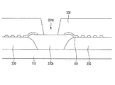
以下、図5乃至図14を参照して、上述した液晶表示装置を製造する一実施形態について説明する。図5、図7、図9及び図13は、図1の切断線II−IIに沿った断面図を順に示したものであり、図6、図8、図10、図11、図12及び図14は、図1の切断線III−IIIに沿った断面図を順に示したものである。 Hereinafter, an embodiment for manufacturing the above-described liquid crystal display device will be described with reference to FIGS. 5, 7, 9, and 13 sequentially show cross-sectional views taken along section line II-II in FIG. 1, and FIGS. 6, 8, 10, 11, 12, and 12. 14 shows the cross-sectional views along the cutting line III-III in FIG. 1 in order.
図5及び図6を参照すれば、透明なガラス又はプラスチックなどからなる基板110の上に薄膜トランジスタQa、Qb、Qc(図1に示した)を形成する。薄膜トランジスタQa、Qb、Qcの上に画素領域に対応するように複数の有機膜230の部分を形成し、隣接する有機膜230の部分の間に遮光部材220a、220bを形成する。
Referring to FIGS. 5 and 6, thin film transistors Qa, Qb, and Qc (shown in FIG. 1) are formed on a
以降、有機膜230の上に、図1に示したように、微細枝部194a、194bを含む画素電極191を形成する。画素電極191は、ITO又はIZOなどの透明導電体から形成される。
画素電極191の上にシリコンオキシカーバイド(SiOC)又はフォトレジストを含む犠牲膜300を形成する。犠牲膜300は他の実施形態では、シリコンオキシカーバイド(SiOC)及びフォトレジストではない有機物質から形成される。
Thereafter, the
A
犠牲膜300がシリコンオキシカーバイド(SiOC)を含む場合には化学気相蒸着法によって形成でき、フォトレジストを含む場合にはコーティング法によって形成できる。犠牲膜300はパターニングされて、薄膜トランジスタの一端子と接続されている信号線と平行な方向に沿ってグルーブGRVが形成され、グルーブGRVと実質的に垂直方向に沿ってオープン部OPNが形成される。
When the
図7及び図8を参照すれば、犠牲膜300の上に順次に共通電極270、蓋膜250、及び支持部材260を形成する。
共通電極270はITO又はIZOなどの透明導電体から形成され、蓋膜250は、窒化ケイ素(SiNx)又は酸化ケイ素(SiO2)から形成される。本実施形態による支持部材260は、上記の犠牲膜300とは異なる物質で形成され得る。
Referring to FIGS. 7 and 8, the
The
共通電極270、蓋膜250、及び支持部材260は、犠牲膜300の上に全面的に形成され、オープン部OPNを満たすように形成される。但し、犠牲膜300を除去するための通路を確保するために、共通電極270、蓋膜250、及び支持部材260は横遮光部材220aと重なる部分から除去される。しかし、犠牲膜300を除去するための通路さえ確保できれば、グルーブGRV内に共通電極270、蓋膜250、及び支持部材260の一部が残っていることが許容される。
The
図9及び図10を参照すれば、グルーブGRVを通じて犠牲膜300をO2アッシング(Ashing)又はウェットエッチング法などによって除去する。このとき、液晶注入口Aを有する微細空間層400が形成される。微細空間層400は犠牲膜300が除去されて形成された空の空間である。液晶注入口Aは、薄膜トランジスタの一端子と接続されている信号線と平行な方向に沿って形成される。
Referring to FIGS. 9 and 10, the
図11を参照すれば、微細空間層400に酸素を含むプラズマ処理PPを施す。プラズマ処理PPによって微細空間層400を取り囲んでいる画素電極191の表面及び共通電極270の表面は親水性を有する。ここで、プラズマ処理PPに用いられる酸素が含まれているガスはO2、O3、NO、N2O、CO、CO2を含む。例えば、プラズマ処理PPを施すときの工程圧力は、10−3トル(torr)乃至10トル(torr)の範囲にあり、工程温度は、−20℃乃至+氏80℃の間にあり、注入されるガスの流量は、10sccm(standard cubic centimeter per minute)乃至10000sccmの範囲にある。
Referring to FIG. 11, the
後続工程において、配向物質をグルーブGRV内に注入すれば、毛管力(capillary force)によって配向物質が液晶注入口Aを通じて微細空間層400の内部に入る。このとき、微細空間層400の内壁が上述のように親水性を有するので、配向物質が乾燥されながら固形分は何れか一つのところに固まる(coalesce)ことなく分散する。従って、乾燥された配向物質が液晶注入口Aを塞いで液晶物質の注入を妨げる恐れ(risk)が減少する。
In the subsequent process, if the alignment material is injected into the groove GRV, the alignment material enters the inside of the
プラズマ処理PPは、微細空間層400の内壁に親水性を持たせるようにするだけでなく、支持部材260又は保護膜240の表面にも影響を与えて、支持部材260又は保護膜240の表面に親水性を持たせる。
The plasma treatment PP not only makes the inner wall of the
図12を参照すれば、隣接する微細空間層400の領域の間に第2疎水性膜275aを形成し、支持部材260又は保護膜240の上に第1疎水性膜275bを形成する。具体的に、第2疎水性膜275aは、横遮光部材220aと重なる部分に形成され、第1疎水性膜270bは、支持部材260の上部面の上に位置する第1部分275b1と、第1部分275b1から延在してグルーブGRV内の側面に沿って位置する第2部分275b2とを含むように形成される。
Referring to FIG. 12, the second
第2疎水性膜275a及び第1疎水性膜270bは炭素、水素又はフッ素を含み、化学気相蒸着法又はスパッタリング方法などを使用して形成できる。スパッタリング方法によって第2疎水性膜275a及び第1疎水性膜270bを形成する場合、例えば、工程圧力は、10−2トル(torr)乃至10トル(torr)の範囲にあり、工程温度は、20℃乃至300℃の間にあり、注入されるガスの流量は、10sccm(standard cubic centimeter per minute)乃至10000sccmの範囲にある。
The second
第2疎水性膜275a及び第1疎水性膜270bは、後で、液晶注入口Aを通じて液晶物質が注入されるとき、液晶物質を分散しないので、液晶物質に含まれている液晶分子310の元の形状が維持される。
Since the second
図13及び図14を参照すれば、グルーブGRVと液晶注入口Aを通じて配向物質を注入して、画素電極191及び共通電極270の内面上に各々配向膜11、21を形成する。配向物質を液晶注入口Aに滴下すると、毛管力によって配向物質が微細空間層400に注入される。本実施形態では第2、第1疎水性膜275a、275bを形成した後に配向膜11、21を形成する場合を説明しているが、他の実施形態では、プラズマ処理PPを施した後に配向膜11、21を形成し、その後で第2、第1疎水性膜275a、275bを形成するように工程順序を変更する。
Referring to FIGS. 13 and 14, an alignment material is injected through the groove GRV and the liquid crystal injection port A, thereby forming
次に、グルーブGRV及び液晶注入口Aを通じて毛管力(capillary force)を利用して微細空間層400に液晶分子310を含む液晶物質を注入する。本実施形態では液晶注入口Aに隣接した領域に第2疎水性膜275aが形成されているので、液晶物質を注入するとき、液晶物質が分散せずに液晶物質に含まれている液晶分子310が元の形状を維持しながら微細空間層400に注入される。また、本実施形態ではグルーブGRVに近く位置する支持部材260の上部面の上に第1疎水性膜275bが形成されている。従って、液晶物質の注入するとき、ミスアラインが発生しても、液晶分子310の元の形状を維持しながら液晶物質を液晶注入口Aに向かって移動するように誘導できる。
Next, a liquid crystal material including the liquid crystal molecules 310 is injected into the
次に、液晶注入口Aには上記注入された液晶物質が外部に露出しているので、液晶注入口Aを覆うようにキャッピング膜280を形成して、図2及び図3の実施形態による液晶表示装置を形成する。このとき、キャッピング膜280は、支持部材260の上部面及び側壁を覆うと共に、グルーブGRVによって露出した微細空間層400の液晶注入口Aを覆う。また、グルーブGRVで第2疎水性膜275aとキャッピング膜280が接触してもよい。
Next, since the injected liquid crystal material is exposed to the liquid crystal inlet A, a
キャッピング膜280は例えば、熱硬化性樹脂、シリコンオキシカーバイド(SiOC)又はグラフェン(Graphene)から形成される。
The
以上、本発明の好ましい実施形態について詳細に説明したが、本発明の権利範囲はこれに限定されず、特許請求の範囲で定義された本発明の基本概念を利用した当業者による種々の変形及び改良形態も本発明の権利範囲に属する。 The preferred embodiments of the present invention have been described in detail above, but the scope of the present invention is not limited thereto, and various modifications and variations by those skilled in the art using the basic concept of the present invention defined in the claims. Improvements are also within the scope of the present invention.
11、12 下部、上部配向膜
110 基板
121a、121b ゲート線、減圧ゲート線
124a、124b、124c 第1、第2、第3ゲート電極
131、129、134、127、137 維持電極線、維持電極、一対の縦部、横部、容量電極
154a、154b、154c 第1、第2、第3半導体
171、173a、173b、173c データ線、第1ソース電極、第2ソース電極、第3ソース電極
175a、175b、175c 第1、第2、第3ドレイン電極
185a、185b コンタクトホール
191、191a、191b 画素電極、第1、第2副画素電極
192a、192b 縦幹部
193a、193b 横幹部
194a、194b 微細枝部
197a、197b 下端、上端突出部
220、220a、220b 遮光部材、横遮光部材、縦遮光部材
230 有機膜(カラーフィルタ)
240 保護膜
250 蓋膜
260 支持部材
270 共通電極
275a 第2疎水性膜
275b、275b1、275b2 第1疎水性膜、第1疎水性膜の第1部分、第1疎水性膜の第2部分
280 キャッピング膜
300 犠牲膜
310 液晶分子
400 微細空間層
11, 12 Lower,
240
Claims (20)
前記基板上に配置された薄膜トランジスタと、
前記薄膜トランジスタの一端子と接続する画素電極と、
前記画素電極上に配置された微細空間層(microcavity)であって、液晶注入口をその端部に備える微細空間層と、
前記微細空間層上に配置された支持部材と、
前記支持部材の少なくとも端部上に配置された第1疎水性膜と、
前記支持部材上に配置されて、前記液晶注入口を覆うキャッピング膜と、を含む、ことを特徴とする液晶表示装置。 A substrate,
A thin film transistor disposed on the substrate;
A pixel electrode connected to one terminal of the thin film transistor;
A micro space layer disposed on the pixel electrode, the micro space layer having a liquid crystal inlet at an end thereof;
A support member disposed on the fine space layer;
A first hydrophobic membrane disposed on at least an end of the support member;
And a capping film disposed on the support member and covering the liquid crystal injection port.
互いに隣接する前記有機膜の部分の間に配置された遮光部材と、をさらに含み、
前記第2疎水性膜は前記遮光部材と重なる、ことを特徴とする請求項5に記載の液晶表示装置。 A plurality of organic film portions disposed on the substrate;
A light shielding member disposed between the portions of the organic film adjacent to each other, and
The liquid crystal display device according to claim 5, wherein the second hydrophobic film overlaps the light shielding member.
前記薄膜トランジスタの上に画素電極を形成する段階と、
前記画素電極上に犠牲膜を形成する段階と、
前記犠牲膜上に支持部材を形成する段階と、
前記犠牲膜を除去して、液晶注入口をその端部に備える微細空間層を形成する段階と、
前記支持部材の少なくとも端部上に第1疎水性膜を形成する段階と、
前記微細空間層に液晶物質を注入する段階と、
前記支持部材上に前記液晶注入口を覆うようにキャッピング膜を形成する段階と、を含む、ことを特徴とする液晶表示装置の製造方法。 Forming a thin film transistor on the substrate;
Forming a pixel electrode on the thin film transistor;
Forming a sacrificial layer on the pixel electrode;
Forming a support member on the sacrificial film;
Removing the sacrificial film and forming a fine space layer with a liquid crystal inlet at its end;
Forming a first hydrophobic membrane on at least an end of the support member;
Injecting a liquid crystal material into the fine space layer;
Forming a capping film on the support member so as to cover the liquid crystal injection port, and a method for manufacturing a liquid crystal display device.
隣接する前記有機膜の部分の間に遮光部材を形成する段階と、をさらに含み、
前記第2疎水性膜は前記遮光部材と重なるように形成する、ことを特徴とする請求項16に記載の液晶表示装置の製造方法。 Forming an organic film comprising a plurality of portions on the substrate;
Further comprising the step of forming a light shielding member between adjacent organic film portions,
The method of manufacturing a liquid crystal display device according to claim 16, wherein the second hydrophobic film is formed to overlap the light shielding member.
20. The method of manufacturing a liquid crystal display device according to claim 19, wherein the hydrophilic treatment step further includes a step of performing a plasma treatment including oxygen.
Applications Claiming Priority (2)
| Application Number | Priority Date | Filing Date | Title |
|---|---|---|---|
| KR10-2012-0132573 | 2012-11-21 | ||
| KR1020120132573A KR20140065271A (en) | 2012-11-21 | 2012-11-21 | Liquid crystal display and manufacturing method thereof |
Publications (2)
| Publication Number | Publication Date |
|---|---|
| JP2014102500A true JP2014102500A (en) | 2014-06-05 |
| JP2014102500A5 JP2014102500A5 (en) | 2016-12-15 |
Family
ID=50727620
Family Applications (1)
| Application Number | Title | Priority Date | Filing Date |
|---|---|---|---|
| JP2013222927A Pending JP2014102500A (en) | 2012-11-21 | 2013-10-28 | Liquid crystal display and method for manufacturing the same |
Country Status (4)
| Country | Link |
|---|---|
| US (1) | US9405156B2 (en) |
| JP (1) | JP2014102500A (en) |
| KR (1) | KR20140065271A (en) |
| CN (1) | CN103838040A (en) |
Cited By (1)
| Publication number | Priority date | Publication date | Assignee | Title |
|---|---|---|---|---|
| US10459272B2 (en) | 2014-10-22 | 2019-10-29 | Samsung Display Co., Ltd. | Liquid crystal display including blocking film |
Families Citing this family (8)
| Publication number | Priority date | Publication date | Assignee | Title |
|---|---|---|---|---|
| KR20140095120A (en) | 2013-01-16 | 2014-08-01 | 삼성디스플레이 주식회사 | Display device and manufacturing method thereof |
| KR20150058910A (en) * | 2013-11-21 | 2015-05-29 | 삼성디스플레이 주식회사 | Display device and manufacturing method thereof |
| KR20150140460A (en) * | 2014-06-05 | 2015-12-16 | 삼성디스플레이 주식회사 | Liquid crystal display and method of manufacturing the same |
| US10330999B2 (en) * | 2014-09-22 | 2019-06-25 | Samsung Display Co., Ltd. | Display panel and method of manufacturing the same |
| KR20160038199A (en) | 2014-09-29 | 2016-04-07 | 삼성디스플레이 주식회사 | Display device and manufacturing method thereof |
| KR20160086529A (en) * | 2015-01-09 | 2016-07-20 | 삼성디스플레이 주식회사 | Liquid crystal display and manufacturing method thereof |
| CN108962936B (en) * | 2017-12-11 | 2021-03-30 | 广东聚华印刷显示技术有限公司 | Pixel defining structure, manufacturing method thereof and display panel |
| TWI706194B (en) * | 2019-09-06 | 2020-10-01 | 友達光電股份有限公司 | Liquid crystal panel and manufacturing method thereof |
Citations (2)
| Publication number | Priority date | Publication date | Assignee | Title |
|---|---|---|---|---|
| JPS60175028A (en) * | 1984-02-21 | 1985-09-09 | Seiko Epson Corp | Manufacture of liquid crystal display element |
| US20120062448A1 (en) * | 2010-09-10 | 2012-03-15 | Kim Yeun Tae | Display apparatus and manufacturing method thereof |
Family Cites Families (19)
| Publication number | Priority date | Publication date | Assignee | Title |
|---|---|---|---|---|
| KR100389889B1 (en) | 1995-04-29 | 2003-10-17 | 삼성전자주식회사 | Method of injecting polymer-liquid crystal compound into liquid crystal display |
| US6141072A (en) | 1997-04-04 | 2000-10-31 | Georgia Tech Research Corporation | System and method for efficient manufacturing of liquid crystal displays |
| JP2000330130A (en) | 1999-05-18 | 2000-11-30 | Advanced Display Inc | Liquid crystal display device and its production |
| JP2004514934A (en) | 2000-12-14 | 2004-05-20 | コーニンクレッカ フィリップス エレクトロニクス エヌ ヴィ | Liquid crystal display laminate and method of manufacturing the same |
| KR20030063656A (en) | 2002-01-23 | 2003-07-31 | 김재훈 | Liquid crystal display and method of manufacturing thereof |
| KR100475164B1 (en) * | 2002-05-16 | 2005-03-08 | 엘지.필립스 엘시디 주식회사 | Liquid Crystal Display and Method of Fabricating the same |
| JP2004212609A (en) * | 2002-12-27 | 2004-07-29 | Dainippon Printing Co Ltd | Liquid crystal display and its manufacturing method |
| JP4145729B2 (en) | 2003-06-13 | 2008-09-03 | セイコーエプソン株式会社 | Manufacturing method of liquid crystal device |
| TWI223113B (en) | 2003-07-24 | 2004-11-01 | Ind Tech Res Inst | Method for manufacturing liquid crystal display device |
| KR101002332B1 (en) * | 2003-12-30 | 2010-12-17 | 엘지디스플레이 주식회사 | Liquid Crystal Display Device And Method For Fabricating The Same |
| WO2006026351A1 (en) * | 2004-08-26 | 2006-03-09 | Applera Corporation | Electrowetting dispensing devices and related methods |
| US8233130B2 (en) * | 2004-12-07 | 2012-07-31 | Industrial Technology Research Institute | Display panel and fabricating method thereof |
| US7573537B2 (en) * | 2005-01-17 | 2009-08-11 | Samsung Electronics Co., Ltd. | Array substrate, liquid crystal display panel having the same and liquid crystal display device having the same |
| JP2008003325A (en) * | 2006-06-22 | 2008-01-10 | Kyocera Mita Corp | Image forming apparatus and image forming program |
| JP4953166B2 (en) | 2007-11-29 | 2012-06-13 | カシオ計算機株式会社 | Manufacturing method of display panel |
| US20090236627A1 (en) * | 2008-03-19 | 2009-09-24 | Jang-Sub Kim | Method of forming metal wiring |
| US8223426B2 (en) * | 2008-12-19 | 2012-07-17 | Motorola Mobility, Inc. | Method and apparatus for providing a decorative surface |
| TW201224507A (en) * | 2010-12-13 | 2012-06-16 | Ind Tech Res Inst | Electrofluidic device and operation method thereof |
| CN102692763B (en) * | 2011-03-23 | 2015-01-07 | 黄继远 | Manufacturing method of flexible display panel |
-
2012
- 2012-11-21 KR KR1020120132573A patent/KR20140065271A/en not_active Application Discontinuation
-
2013
- 2013-07-09 US US13/938,106 patent/US9405156B2/en active Active
- 2013-08-30 CN CN201310388992.5A patent/CN103838040A/en active Pending
- 2013-10-28 JP JP2013222927A patent/JP2014102500A/en active Pending
Patent Citations (2)
| Publication number | Priority date | Publication date | Assignee | Title |
|---|---|---|---|---|
| JPS60175028A (en) * | 1984-02-21 | 1985-09-09 | Seiko Epson Corp | Manufacture of liquid crystal display element |
| US20120062448A1 (en) * | 2010-09-10 | 2012-03-15 | Kim Yeun Tae | Display apparatus and manufacturing method thereof |
Cited By (1)
| Publication number | Priority date | Publication date | Assignee | Title |
|---|---|---|---|---|
| US10459272B2 (en) | 2014-10-22 | 2019-10-29 | Samsung Display Co., Ltd. | Liquid crystal display including blocking film |
Also Published As
| Publication number | Publication date |
|---|---|
| CN103838040A (en) | 2014-06-04 |
| KR20140065271A (en) | 2014-05-29 |
| US20140139795A1 (en) | 2014-05-22 |
| US9405156B2 (en) | 2016-08-02 |
Similar Documents
| Publication | Publication Date | Title |
|---|---|---|
| JP2014102500A (en) | Liquid crystal display and method for manufacturing the same | |
| KR20130107952A (en) | Liquid crystal display and manufacturing method thereof | |
| US9500913B2 (en) | Display device and manufacturing method thereof | |
| JP2014106531A (en) | Liquid crystal display device and manufacturing method thereof | |
| KR101663595B1 (en) | Liquid crystal display device and manufacturing method thereof | |
| JP2014139652A (en) | Liquid Crystal Display | |
| KR20140112288A (en) | Liquid crystal display and method of manufacturing the same | |
| US9625753B2 (en) | Liquid crystal display and method of manufacturing the same | |
| JP2015018248A (en) | Liquid crystal display and manufacturing method thereof | |
| KR20140115180A (en) | Liquid crystal displsy and method for manufacturing the same | |
| KR20150015766A (en) | Display device and manufacturing method thereof | |
| CN104849915A (en) | Liquid crystal display and method of manufacturing the same | |
| US9606402B2 (en) | Liquid crystal display having injection holes with different heights and method of manufacturing the same | |
| KR20150007175A (en) | Display device and manufacturing method thereof | |
| US9785002B2 (en) | Liquid crystal display and method of manufacturing the same | |
| KR20150020909A (en) | Liquid crystal display and method of manufacturing the same | |
| JP2015135466A (en) | Display device, and method for manufacturing the same | |
| KR20150058661A (en) | Liquid crystal display and method of manufacturing the same | |
| KR101701402B1 (en) | Liquid crystal display device and manufacturing method thereof | |
| US10539838B2 (en) | Liquid crystal display device and related manufacturing method | |
| KR101731048B1 (en) | Liquid crystal display device and manufacturing method thereof | |
| KR20160038199A (en) | Display device and manufacturing method thereof | |
| KR20160047031A (en) | Display device and manufacturing method thereof | |
| KR20150086127A (en) | Liquid crystal display | |
| KR20160085390A (en) | Display device and manufacturing method thereof |
Legal Events
| Date | Code | Title | Description |
|---|---|---|---|
| A521 | Request for written amendment filed |
Free format text: JAPANESE INTERMEDIATE CODE: A523 Effective date: 20161026 |
|
| A621 | Written request for application examination |
Free format text: JAPANESE INTERMEDIATE CODE: A621 Effective date: 20161026 |
|
| A131 | Notification of reasons for refusal |
Free format text: JAPANESE INTERMEDIATE CODE: A131 Effective date: 20170919 |
|
| A977 | Report on retrieval |
Free format text: JAPANESE INTERMEDIATE CODE: A971007 Effective date: 20170920 |
|
| A02 | Decision of refusal |
Free format text: JAPANESE INTERMEDIATE CODE: A02 Effective date: 20180410 |