JP2014010169A - Multi-display device and method for manufacturing multi-display device - Google Patents
Multi-display device and method for manufacturing multi-display device Download PDFInfo
- Publication number
- JP2014010169A JP2014010169A JP2012144509A JP2012144509A JP2014010169A JP 2014010169 A JP2014010169 A JP 2014010169A JP 2012144509 A JP2012144509 A JP 2012144509A JP 2012144509 A JP2012144509 A JP 2012144509A JP 2014010169 A JP2014010169 A JP 2014010169A
- Authority
- JP
- Japan
- Prior art keywords
- liquid crystal
- crystal display
- panel
- display device
- panels
- Prior art date
- Legal status (The legal status is an assumption and is not a legal conclusion. Google has not performed a legal analysis and makes no representation as to the accuracy of the status listed.)
- Pending
Links
Images


Classifications
-
- G—PHYSICS
- G02—OPTICS
- G02F—OPTICAL DEVICES OR ARRANGEMENTS FOR THE CONTROL OF LIGHT BY MODIFICATION OF THE OPTICAL PROPERTIES OF THE MEDIA OF THE ELEMENTS INVOLVED THEREIN; NON-LINEAR OPTICS; FREQUENCY-CHANGING OF LIGHT; OPTICAL LOGIC ELEMENTS; OPTICAL ANALOGUE/DIGITAL CONVERTERS
- G02F1/00—Devices or arrangements for the control of the intensity, colour, phase, polarisation or direction of light arriving from an independent light source, e.g. switching, gating or modulating; Non-linear optics
- G02F1/01—Devices or arrangements for the control of the intensity, colour, phase, polarisation or direction of light arriving from an independent light source, e.g. switching, gating or modulating; Non-linear optics for the control of the intensity, phase, polarisation or colour
- G02F1/13—Devices or arrangements for the control of the intensity, colour, phase, polarisation or direction of light arriving from an independent light source, e.g. switching, gating or modulating; Non-linear optics for the control of the intensity, phase, polarisation or colour based on liquid crystals, e.g. single liquid crystal display cells
- G02F1/133—Constructional arrangements; Operation of liquid crystal cells; Circuit arrangements
- G02F1/1333—Constructional arrangements; Manufacturing methods
- G02F1/13336—Combining plural substrates to produce large-area displays, e.g. tiled displays
-
- G—PHYSICS
- G02—OPTICS
- G02F—OPTICAL DEVICES OR ARRANGEMENTS FOR THE CONTROL OF LIGHT BY MODIFICATION OF THE OPTICAL PROPERTIES OF THE MEDIA OF THE ELEMENTS INVOLVED THEREIN; NON-LINEAR OPTICS; FREQUENCY-CHANGING OF LIGHT; OPTICAL LOGIC ELEMENTS; OPTICAL ANALOGUE/DIGITAL CONVERTERS
- G02F1/00—Devices or arrangements for the control of the intensity, colour, phase, polarisation or direction of light arriving from an independent light source, e.g. switching, gating or modulating; Non-linear optics
- G02F1/01—Devices or arrangements for the control of the intensity, colour, phase, polarisation or direction of light arriving from an independent light source, e.g. switching, gating or modulating; Non-linear optics for the control of the intensity, phase, polarisation or colour
- G02F1/13—Devices or arrangements for the control of the intensity, colour, phase, polarisation or direction of light arriving from an independent light source, e.g. switching, gating or modulating; Non-linear optics for the control of the intensity, phase, polarisation or colour based on liquid crystals, e.g. single liquid crystal display cells
- G02F1/133—Constructional arrangements; Operation of liquid crystal cells; Circuit arrangements
- G02F1/1333—Constructional arrangements; Manufacturing methods
- G02F1/133351—Manufacturing of individual cells out of a plurality of cells, e.g. by dicing
-
- G—PHYSICS
- G06—COMPUTING; CALCULATING OR COUNTING
- G06F—ELECTRIC DIGITAL DATA PROCESSING
- G06F3/00—Input arrangements for transferring data to be processed into a form capable of being handled by the computer; Output arrangements for transferring data from processing unit to output unit, e.g. interface arrangements
- G06F3/14—Digital output to display device ; Cooperation and interconnection of the display device with other functional units
- G06F3/1423—Digital output to display device ; Cooperation and interconnection of the display device with other functional units controlling a plurality of local displays, e.g. CRT and flat panel display
- G06F3/1446—Digital output to display device ; Cooperation and interconnection of the display device with other functional units controlling a plurality of local displays, e.g. CRT and flat panel display display composed of modules, e.g. video walls
-
- G—PHYSICS
- G09—EDUCATION; CRYPTOGRAPHY; DISPLAY; ADVERTISING; SEALS
- G09G—ARRANGEMENTS OR CIRCUITS FOR CONTROL OF INDICATING DEVICES USING STATIC MEANS TO PRESENT VARIABLE INFORMATION
- G09G2320/00—Control of display operating conditions
- G09G2320/02—Improving the quality of display appearance
- G09G2320/0233—Improving the luminance or brightness uniformity across the screen
Abstract
Description
本発明は、複数の液晶表示パネルを並置して映像を表示するマルチディスプレイ装置及びマルチディスプレイ装置の製造方法に関する。 The present invention relates to a multi-display device that displays a video by juxtaposing a plurality of liquid crystal display panels, and a method for manufacturing the multi-display device.
液晶表示装置は、コンピュータのディスプレイ、テレビジョン受像機、及び各種の情報を表示する情報ディスプレイ等に広く利用されている。
近年、複数の表示パネルを並置して、それぞれの表示パネルに1枚の画像の一部ずつを表示することによって、大画面表示を行うマルチディスプレイ装置が開発されている(例えば、特許文献1を参照)。このマルチディスプレイ装置を構成する表示パネルには、液晶表示パネルが利用されることがある。
Liquid crystal display devices are widely used for computer displays, television receivers, information displays for displaying various information, and the like.
In recent years, a multi-display device that displays a large screen by arranging a plurality of display panels in parallel and displaying a part of one image on each display panel has been developed (for example, see Patent Document 1). reference). A liquid crystal display panel may be used as a display panel constituting the multi-display device.
公共スペースに設置された情報ディスプレイ等、多数の視聴者に表示画像が閲覧される表示装置では、画質が保たれるように、画面を均一にしておくことが好ましい。複数の表示パネルを使用するマルチディスプレイ装置では、表示パネルと表示パネルとの間に境界が存在しており、各表示パネルの個体のばらつきに伴い、境界付近で画質が明らかに不連続となるといった問題が生じていた。 In a display device in which a display image is viewed by a large number of viewers such as an information display installed in a public space, it is preferable that the screen is uniform so that the image quality is maintained. In a multi-display device using a plurality of display panels, there is a boundary between the display panels, and the image quality is clearly discontinuous in the vicinity of the boundary due to individual variations of each display panel. There was a problem.
本発明は、斯かる事情に鑑みてなされたものであり、液晶表示パネルを複数備え、画面を均一にすることができるマルチディスプレイ装置及びマルチディスプレイ装置の製造方法を提供することを目的とする。 The present invention has been made in view of such circumstances, and an object of the present invention is to provide a multi-display device and a method for manufacturing the multi-display device that include a plurality of liquid crystal display panels and can make the screen uniform.
本発明に係るマルチディスプレイ装置は、複数の液晶表示パネルを並置してあり、入力された映像信号に基づいて、各液晶表示パネルに映像を表示するマルチディスプレイ装置において、前記複数の液晶表示パネルのうち少なくとも2つは、液晶物質を封入するための空隙が形成された一のパネル部材から切り出して製造したものであることを特徴とする。 A multi-display device according to the present invention includes a plurality of liquid crystal display panels juxtaposed, and a multi-display device that displays an image on each liquid crystal display panel based on an input video signal. At least two of them are manufactured by cutting out from one panel member in which a gap for enclosing a liquid crystal substance is formed.
液晶表示パネルのセル厚は、数μm程度の厚みであり、100分の1μm程度の差で、色度及び輝度が変化する。液晶物質を封入するための空隙は、パネル部材(マザーパネル)を作成する際に、2枚のガラス基板を貼り合わせることで形成されるので、同一のパネル部材におけるセル厚のばらつきよりも、別のパネル部材との間のばらつきの方が大きくなる。本発明では、マルチディスプレイ装置を構成する複数の液晶表示パネルのうち、少なくとも2つを、同一のパネル部材より切り出して製造したものを用いているので、全体的に色度及び輝度が均一となる。 The cell thickness of the liquid crystal display panel is about several μm, and the chromaticity and luminance change with a difference of about 1/100 μm. Since the gap for enclosing the liquid crystal substance is formed by bonding two glass substrates when creating a panel member (mother panel), it is different from the cell thickness variation in the same panel member. The variation between the panel members becomes larger. In the present invention, since at least two of the plurality of liquid crystal display panels constituting the multi-display device are manufactured by cutting out from the same panel member, chromaticity and luminance are uniform throughout. .
本発明に係るマルチディスプレイ装置は、前記複数の液晶表示パネルのうち、隣り合う2つの液晶表示パネルを前記一のパネル部材から製造した液晶表示パネルとしてあることを特徴とする。 The multi-display device according to the present invention is characterized in that, among the plurality of liquid crystal display panels, two adjacent liquid crystal display panels are liquid crystal display panels manufactured from the one panel member.
本発明にあっては、隣り合う液晶表示パネルの境界付近における色度及び輝度の差が小さくなり、液晶表示パネル間での画質の不連続性が緩和される。 In the present invention, the difference in chromaticity and brightness near the boundary between adjacent liquid crystal display panels is reduced, and the discontinuity in image quality between the liquid crystal display panels is alleviated.
本発明に係るマルチディスプレイ装置は、前記一のパネル部材での位置関係を維持して、少なくとも2つの液晶表示パネルを並置するようにしてあることを特徴とする。 The multi-display device according to the present invention is characterized in that at least two liquid crystal display panels are juxtaposed while maintaining the positional relationship of the one panel member.
本発明にあっては、パネル部材から切り出したパネルの位置関係を維持して液晶表示パネルを配置するので、液晶表示パネル間の色度及び輝度の不連続性を抑制することができる。 In the present invention, since the liquid crystal display panel is arranged while maintaining the positional relationship of the panels cut out from the panel member, chromaticity and luminance discontinuity between the liquid crystal display panels can be suppressed.
本発明に係るマルチディスプレイ装置は、各液晶表示パネルには、該液晶表示パネルを切り出したパネル部材を特定するための情報を記録してあることを特徴とする。 The multi-display device according to the present invention is characterized in that information for specifying a panel member from which the liquid crystal display panel is cut out is recorded in each liquid crystal display panel.
本発明にあっては、各液晶表示パネルに記録されている情報を参照することによって、同一のパネル部材から切り出して製造した液晶表示パネルを特定することができる。 In the present invention, by referring to information recorded in each liquid crystal display panel, it is possible to specify a liquid crystal display panel that is cut out from the same panel member and manufactured.
本発明に係るマルチディスプレイ装置の製造方法は、複数の液晶表示パネルを並置してあり、入力された映像信号に基づいて、各液晶表示パネルに映像を表示するマルチディスプレイ装置の製造方法において、前記複数の液晶表示パネルのうちの少なくとも2つを、液晶物質を封入するための空隙が形成された一のパネル部材から切り出して製造し、前記一のパネル部材から切り出して製造した少なくとも2つの液晶表示パネルを並置することを特徴とする。 A method for manufacturing a multi-display device according to the present invention is the method for manufacturing a multi-display device in which a plurality of liquid crystal display panels are juxtaposed and an image is displayed on each liquid crystal display panel based on an input video signal. At least two liquid crystal displays manufactured by cutting at least two of the plurality of liquid crystal display panels from one panel member in which a gap for enclosing a liquid crystal material is formed and cutting out from the one panel member It is characterized by juxtaposing the panels.
本発明では、同一のパネル部材から切り出した液晶表示パネルを並置してマルチディスプレイ装置を製造するので、このマルチディスプレイ装置が備える画面は全体的に色度及び輝度が均一なものとなる。 In the present invention, a multi-display device is manufactured by juxtaposing liquid crystal display panels cut out from the same panel member. Therefore, the screen provided in the multi-display device has uniform chromaticity and luminance as a whole.
本発明によれば、マルチディスプレイ装置を構成する複数の液晶表示パネルのうち、少なくとも2つを、同一のパネル部材より切り出して製造したものを用いているので、パネル間の境界における色度及び輝度の差を小さくすることができ、画質の不連続性を緩和することができる。 According to the present invention, at least two of the plurality of liquid crystal display panels constituting the multi-display device are manufactured by cutting out from the same panel member, so that the chromaticity and luminance at the boundary between the panels are used. Difference can be reduced, and discontinuity in image quality can be reduced.
本発明をその実施の形態を示す図面に基づいて具体的に説明する。
実施の形態1.
図1は実施の形態1に係るマルチディスプレイ装置の構成例を示す模式図である。実施の形態1に係るマルチディスプレイ装置は、2枚の液晶表示パネル10,10を並べて構成した表示装置である。図1に示す構成例は、矩形状の液晶表示パネル10を上下方向に並べたものである。マルチディスプレイ装置は、入力された映像信号に基づく1つの映像を、2枚の液晶表示パネル10,10に分割して表示することにより、大画面の表示を行う。
The present invention will be specifically described with reference to the drawings showing the embodiments thereof.
Embodiment 1 FIG.
FIG. 1 is a schematic diagram illustrating a configuration example of a multi-display device according to the first embodiment. The multi-display device according to Embodiment 1 is a display device configured by arranging two liquid
図2はマルチディスプレイ装置の制御系の構成を示すブロック図である。図2では各液晶表示パネル10の制御系の構成を示している。各液晶表示パネル10は、例えば、映像信号入力部101、映像信号処理部102、色信号補正部103、LCD/LEDデータ処理部104、LCDタイミングコントローラ105、ソースドライバ106、ゲートドライバ107、LEDバックライトタイミングコントローラ108、LEDドライバ109、及び制御部110により制御される。
FIG. 2 is a block diagram showing the configuration of the control system of the multi-display apparatus. FIG. 2 shows the configuration of the control system of each liquid
マルチディスプレイ装置には、例えば、HDMI、コンポジット、D端子などの映像入力端子(不図示)を通じて外部より映像信号が入力される。マルチディスプレイ装置は、各液晶表示パネル10の表示サイズに合わせて分割した映像が各液晶表示パネル10にそれぞれ表示されるように、外部から入力された映像信号に基づき、各液晶表示パネル用の映像信号を生成する。映像信号入力部101には、マルチディスプレイ装置が生成した各液晶表示パネル用の信号が入力される。
For example, a video signal is input to the multi-display device from the outside through a video input terminal (not shown) such as HDMI, composite, and D terminal. The multi-display device uses a video signal for each liquid crystal display panel based on a video signal input from the outside so that the video divided according to the display size of each liquid
映像信号処理部102は、入力された映像信号に対して各種信号処理を行うための処理部である。映像信号処理部102は、例えば、映像信号から水平同期信号及び垂直同期信号を分離する処理、これらの同期信号に位相同期したクロック信号を生成する処理、映像信号からの輝度信号及び色信号を分離する処理等を実行する。また、映像信号処理部102は、ユーザインタフェース用のオンスクリーンディスプレイ(OSD)の重ね合わせなどの適宜の信号処理を施すものであってもよい。
色信号補正部103は、映像信号処理部102を通じて入力される映像信号に対し、彩度、シャープネスといった画像調整処理を施す。
The video
The color
色信号補正部103にて最終的に表示する映像の調整を行った後、LCD/LEDデータ処理部104は、演算により、液晶表示パネル用データ及びバックライト点灯データに分離する。LCD/LEDデータ処理部104は、液晶表示パネル用データをLCDタイミングコントローラ105に、バックライト点灯データをLEDバックライトタイミングコントローラ108に送出する。
After adjustment of the video to be finally displayed by the color
LCDタイミングコントローラ105は、制御部110から与えられるLCD制御信号、及びLCD/LEDデータ処理部104から渡されるデータに基づき、ソースドライバ106及びゲートドライバ107の駆動を制御する。また、LEDバックライトタイミングコントローラ108は、制御部110から与えられるバックライト制御信号、及びLCD/LEDデータ処理部104から渡されるデータに基づき、LEDドライバ109の駆動を制御する。
The
以上のように、マルチディスプレイ装置は、各液晶表示パネル10にて、ソースドライバ106及びゲートドライバ107の駆動を制御し、後述する液晶物質に印加する電圧の大きさを調整すると共に、後述するバックライトユニット30(図5を参照)の点灯及び消灯タイミングを制御することにより、映像表示を行う。
As described above, the multi-display device controls the driving of the
図3はマルチディスプレイ装置に用いる液晶表示パネル10の概略構成を示す模式図である。図3に示す液晶表示パネル10は透過型の液晶表示パネルである。以下、図5を参照しながら説明する。液晶表示パネル10は、TFT12(Thin Film Transistor)、画素電極13などの素子が形成されるガラス基板11(以下、TFT側ガラス基板11ともいう)と、このガラス基板11と対向するように配置され、カラーフィルタ16(CF:Color Filter)、対向電極17などが形成されるガラス基板15(以下、CF側ガラス基板15ともいう)とを備える。2枚のガラス基板11,15の間には空隙が形成され、この空隙内に液晶物質が封入されることによって液晶層20が形成される。液晶表示パネル10は、画素電極13と対向電極17との間に電圧を印加して液晶物質の透過率を制御し、2枚のガラス基板11,15の間を透過する光の光量を調整することによって映像表示を行う。なお、透過型の液晶表示パネル10においてはTFT側ガラス基板11の背面側からバックライトユニット30を用いて光が照射される。
FIG. 3 is a schematic diagram showing a schematic configuration of the liquid
液晶表示パネル10では、画素電極13及び対向電極17に印加する電圧の値を変化させることにより、ガラス基板11,15間の液晶物質の光学的な特性を変化させているが、2枚のガラス基板11,15の間隔(セル厚)が変化した場合にも、液晶物質の光学的な特性は変化する。例えば、セル厚が薄い方から厚い方へ変化するにつれて、紫、青、黄、橙、赤、紫の順に色度が巡回的に変化する。これは、液晶物質の複屈折により、液晶物質の厚みによって光が透過したときのスペクトルが変化するためである。一般的に使用されている液晶材料においてセル厚が3μmの場合、例えば、青色側にシフトした色度を有するが、そこからセル厚が少しだけ(100分の1μm程度)厚くなると黄色側に色度が変化する。また、青色よりも黄色のスペクトルの方が輝度に変換したときの値が大きくなるため、輝度は上昇する。
In the liquid
セル厚は液晶表示パネル10の製造工程のばらつきに起因して変化する。1枚の液晶表示パネル10のみにより構成される表示装置では、画面全体で色度及び輝度が連続的に変化するため、表示品質に大きな問題は存在しない。ところが、複数の液晶表示パネル10,10を並べて構成するマルチディスプレイ装置では、セル厚が異なるパネルを用いた場合、画面間で色度及び輝度が異なり、画面の境界(すなわち、隣り合う2つのパネル間の境界)で画像の連続性が失われる。
The cell thickness changes due to variations in the manufacturing process of the liquid
このような課題を解決するために、本実施の形態では、マルチディスプレイ装置を構成する2枚の液晶表示パネル10,10を、1枚のマザーパネルMPから切り出して製造する(図4を参照)。1枚のマザーパネルMP内でのセル厚のばらつきは、複数のマザーパネルMP,MP,…同士のばらつきに比べて小さいので、1枚のマザーパネルMPから切り出したパネルを用いてマルチディスプレイ装置を構成することにより、画面の境界での色度及び輝度の変化を小さくすることができ、画像の連続性を良好に保つことができる。
In order to solve such a problem, in the present embodiment, two liquid
図4はパネルの切り出し工程を説明する模式図である。マザーパネルMPは、TFT側ガラス基板11とCF側ガラス基板15とをシール部材を介して貼り合わせたパネル部材であり、貼り合わせたTFT側ガラス基板11とCF側ガラス基板15との間に液晶物質を封入するための空隙が形成される。液晶物質は、マザーパネルMPの製造段階(パネルを切り出す前)、又は各パネルをマザーパネルMPから切り出した後に封入される。
なお、マザーパネルMPは、公知の手法を用いて製造することができ、例えば、特開2011−145406号公報に開示された手法を用いることができる。
FIG. 4 is a schematic diagram for explaining a panel cutting process. The mother panel MP is a panel member in which the TFT
Note that the mother panel MP can be manufactured using a known method, for example, a method disclosed in Japanese Patent Application Laid-Open No. 2011-145406.
図4では、1枚のマザーパネルMPから6枚のパネルを切り出した例を示している。マザーパネルMPの切り出しには、スクライブブレイク法などの公知の手法、上記公報に開示された手法等を用いることができる。1枚のマザーパネルMP内でのセル厚のばらつきは比較的小さいので、例えば、切り出した6枚のパネルから任意に選択した2枚のパネルを用いて、マルチディスプレイ装置を構成する2枚の液晶表示パネル10,10を製造することができる。
FIG. 4 shows an example in which six panels are cut out from one mother panel MP. For cutting out the mother panel MP, a known method such as a scribe break method, a method disclosed in the above publication, or the like can be used. Since the variation in cell thickness within one mother panel MP is relatively small, for example, two liquid crystals constituting a multi-display device using two panels arbitrarily selected from the cut out six panels. The
図5は液晶表示パネル10の構成を示す模式図である。マザーパネルMPから切り出したパネルは、TFT側ガラス基板11、液晶物質を封入することによって形成される液晶層20、及びCF側ガラス基板15を含むLCDモジュールを構成する。TFT側ガラス基板11には、その一面側に、画素を形成する画素電極13、及び画素電極13に接続されるTFT12、並びに配向膜14が積層される。また、CF側ガラス基板15には、その一面側に、カラーフィルタ16、対向電極17、及び配向膜18が積層される。
FIG. 5 is a schematic diagram showing the configuration of the liquid
このLCDモジュールの背面側(TFT側ガラス基板11の他面側)には、バックライトユニット30、拡散板31及び偏光板32が設けられる。また、LCDモジュールの表面側(CF側ガラス基板15の他面側)には、偏光板33及び保護ガラス40が設けられる。
A
バックライトユニット30は、例えば、側方から導光板に対して光を発する光源と、側方から入射した光をLCDモジュール側に出射する導光板とを有するエッジライト式バックライト、又は、TFT側ガラス基板に対向するように配置した複数のLEDを備える直下型のLEDバックライトにより構成される。
The
偏光板32は、TFT側ガラス基板11の表面に配置され、偏光板33は、CF側ガラス基板15の表面に配置される。偏光板32,33は、互いに直交する直線偏光を透過するように設けられる。
拡散板31は、偏光板32とバックライトユニット30との間に配設され、バックライトユニット30から出射された光を全方向に拡散させる機能を有する。
保護ガラス40は、偏光板33のCF側ガラス基板15に臨む側とは反対側の表面に配置され、LCDモジュールを保護する機能を有する。
The
The
The
このような構成により、バックライトユニット30から出射された光のうち偏光板32を透過した直線偏光は、液晶層20を通過して偏光板33に入射する。このとき、液晶層20を透過する光の偏光状態は、液晶層20に印加する電圧によって変化させることができる。このため映像信号に対応した電圧を、画素電極13及び対向電極17に印加し、液晶層20に電界を印加することで、液晶層20を通過する光の偏光状態を変え、偏光板32を透過する光の光量を制御して、光学画像を形成することができる。
With such a configuration, the linearly polarized light transmitted through the
本実施の形態では、セル厚の不均一性に伴うパネルの色度及び輝度の変化について説明したが、パネルの色度及び輝度の変化が発生する要因は、必ずしもセル厚の不均一性だけではない。例えば、各ガラス基板11,15上に形成される配向膜14,18の膜厚の不均一性に伴って、パネルの色度及び輝度に変化が生じる場合がある。このように、セル厚の不均一性、配向膜14,18の膜厚の不均一性などマザーパネルMPの製造工程に起因した画質の変化がパネルに生じる場合であっても、本実施の形態では、マザーパネルMPを製造した後、1枚のマザーパネルMPから切り出した複数のパネルを用いてマルチディスプレイ装置を構成しているので、パネル間での表示品質の差を小さく抑えることができる。
In this embodiment, the change in the chromaticity and luminance of the panel due to the nonuniformity of the cell thickness has been described. However, the cause of the change in the chromaticity and luminance of the panel is not necessarily the nonuniformity of the cell thickness. Absent. For example, the chromaticity and luminance of the panel may change due to the non-uniformity of the thickness of the
なお、図5では、透過型の液晶表示パネル10について説明したが、反射型の液晶表示パネルを用いてマルチディスプレイ装置を構成するものであってもよい。
Note that although the transmissive liquid
実施の形態2.
実施の形態1では、1枚のマザーパネルMPから切り出した2枚のパネルを用いて、マルチディスプレイ装置を構成したが、マルチディスプレイ装置を構成するパネルの枚数は2枚に限定されるものではない。ただし、1枚のマザーパネルMPから切り出すことができるパネルの枚数には制限があるので、2枚より多くのパネルを用いてマルチディスプレイ装置を構成する場合、それらの全てのパネルを、同一のマザーパネルMPから生成することができるとは限らない。
本実施の形態では、マルチディスプレイ装置を構成する複数の液晶表示パネル10,10,10,…のうち、少なくとも2枚を同一のマザーパネルMPから生成する構成について説明する。
In the first embodiment, the multi-display device is configured using two panels cut out from one mother panel MP. However, the number of panels constituting the multi-display device is not limited to two. . However, since there is a limit to the number of panels that can be cut out from one mother panel MP, when configuring a multi-display device using more than two panels, all those panels must be connected to the same mother panel. It cannot always be generated from the panel MP.
In the present embodiment, a configuration in which at least two of the plurality of liquid
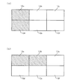
図6は実施の形態2に係るマルチディスプレイ装置の構成例を示す模式図である。図6に示すマルチディスプレイ装置は6枚の液晶表示パネル10a〜10fを備え、上段の横方向に3枚の液晶表示パネル10a,10b,10c、下段の横方向に3枚の液晶表示パネル10d,10e,10fを配置したものである。マルチディスプレイ装置は、入力された映像信号に基づく1つの映像を、6枚の液晶表示パネル10a〜10fに分割して表示することにより、大画面の表示を行う。
なお、各液晶表示パネル10a〜10fの構成は、実施の形態1で説明した液晶表示パネル10と全く同様である。また、マルチディスプレイ装置の制御系の構成についても実施の形態1と全く同様であるので、その説明を省略することとする。
FIG. 6 is a schematic diagram illustrating a configuration example of the multi-display device according to the second embodiment. The multi-display device shown in FIG. 6 includes six liquid
The configuration of each of the liquid
図6(a)に示した例は、6枚の液晶表示パネル10a〜10fのうち、パネル正面から見て左端2枚の液晶表示パネル10a,10dが、1枚のマザーパネルMPから切り出したパネルを用いて製造したものであることを示している。残りの4枚の液晶表示パネル10b,10c,10e,10fについては、他のマザーパネルMPから切り出したパネルを用いて製造される。
In the example shown in FIG. 6A, among the six liquid
図6(b)に示した例では、6枚の液晶表示パネル10a〜10fのうち、パネル正面から見て上段の左側及び中央の液晶表示パネル10a,10bが、1枚のマザーパネルMPから切り出したパネルを用いて製造したものであることを示している。残りの4枚の液晶表示パネル10c〜10fについては、他のマザーパネルMPから切り出したパネルを用いて製造される。
In the example shown in FIG. 6B, among the six liquid
以上のように、実施の形態2では、マルチディスプレイ装置を構成する複数の液晶表示パネル10a〜10fのうち少なくとも2枚を、同一のマザーパネルMPから切り出したものを用いているので、それぞれ異なるマザーパネルMP,MP,…から切り出したパネルを用いたマルチディスプレイ装置と比較して、画質に統一感を与えることができる。
As described above, in the second embodiment, at least two of the plurality of liquid
実施の形態3.
実施の形態1では、1枚のマザーパネルMPから切り出した複数のパネルのうち、任意の2枚を選択して製造した液晶表示パネル10,10を、マルチディスプレイ装置に用いる構成としたが、より好ましくは、切り出したパネルのマザーパネルMPでの位置関係とマルチディスプレイ装置で用いる液晶表示パネル10の位置関係とが同一であることが好ましい。
実施の形態3では、マザーパネルMPから切り出すパネルの位置関係を考慮して、各液晶表示パネル10,10,…を配置する構成について説明を行う。
In the first embodiment, the liquid
In the third embodiment, a configuration in which the liquid
図7は実施の形態3に係るマルチディスプレイ装置の構成例を示す模式図である。実施の形態3に係るマルチディスプレイ装置は、2枚の液晶表示パネル10,10を上下方向に並べて構成した表示装置である。マルチディスプレイ装置は、入力された映像信号に基づく1つの映像を、2枚の液晶表示パネル10,10に分割して表示することにより、大画面の表示を行う。
なお、マルチディスプレイ装置の制御系の構成、及び液晶表示パネル10の構成は実施の形態1と全く同様であるので、その説明を省略することとする。
FIG. 7 is a schematic diagram illustrating a configuration example of the multi-display device according to the third embodiment. The multi-display device according to
Since the configuration of the control system of the multi-display device and the configuration of the liquid
前述したように、2枚のガラス基板11,15の間隔(セル厚)等の違いにより、液晶表示パネル10の光学的な特性(色度及び輝度)は変化する。このようなセル厚の変化が局所的な領域で発生した場合、その領域内での色度及び輝度は、他の領域内の色度及び輝度とずれるため、斑となって画面に表れる。この斑は、セル厚に起因して発生するものであるため、面内での変化は緩やかであり、1枚の液晶表示パネル10で表示する際には大きな問題にはならない。ところが、複数の液晶表示パネル10,10,…を並べて構成するマルチディスプレイ装置では、斑が表れる液晶表示パネル10と、斑が表れない液晶表示パネル10とを隣接して配置した場合、これらのパネル間の境界付近において、色度及び輝度が急激に変化してしまうことになるため、表示画像の連続性が失われることになる。
As described above, the optical characteristics (chromaticity and luminance) of the liquid
このような課題を解決するために、実施の形態3では、マルチディスプレイ装置を構成する2枚の液晶表示パネル10,10を、1枚のマザーパネルMPから切り出して製造し、更に、切り出したパネルのマザーパネルMP上での位置関係とマルチディスプレイ装置での液晶表示パネル10,10の位置関係とが同一となるように、液晶表示パネル10,10の配置を行う。
In order to solve such a problem, in the third embodiment, the two liquid
以上のように、実施の形態3では、切り出したパネルのマザーパネルMP上での位置関係とマルチディスプレイ装置での液晶表示パネル10,10の位置関係とが同一となるように、各液晶表示パネル10,10を配置してマルチディスプレイ装置を製造しているので、2つの液晶表示パネル10,10に跨がるような領域にて画質の変化(斑)が発生している場合であっても、それらを隣接させて配置することにより画質の連続性を良好に保つことができる。
As described above, in the third embodiment, the liquid crystal display panels are arranged so that the positional relationship of the cut-out panel on the mother panel MP and the positional relationship of the liquid
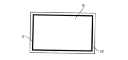
マルチディスプレイ装置を構成する各液晶表示パネル10の周囲にはブラックマトリクスやベゼルが設けられる。図8は各液晶表示パネル10の周囲に存在するブラックマトリクス及びベゼルの一例を示す模式図である。図8に示すように、各液晶表示パネル10の周囲にはブラックマトリクス51及びベゼル52が存在するため、マルチディスプレイ装置の隣り合う液晶表示パネル10,10の間には、狭額縁のディスプレイであっても5〜7mm程度の間隔が存在する。また、図4に示すように、マザーパネルMPからの各パネルを切り出す際、隣り合うパネル同士であっても適宜の間隔を設けて切り出すことがある。マザーパネルMPから切り出すパネルの枚数が最大となるように、マザーパネルMP上の各パネルの配置が決定されるからである。マザーパネルMPから切り出すパネル間の間隔は、必要とされるパネルのサイズ(解像度)、液晶表示パネル10を駆動するドライバの個数及びドライバ全体の出力数、ドライバを駆動する基板を液晶表示パネル10に配置するか否か、各液晶表示パネル10に設けられる接続端子53(図9を参照)の大きさ、ダミーの画素を設けるか否か、ブラックマトリクス51で遮光する領域等の各種要因により定まる。
A black matrix and a bezel are provided around each liquid
このため、切り出したパネルのマザーパネルMP上での位置関係とマルチディスプレイ装置での各液晶表示パネル10,10,…の位置関係とが同一となるように配置したとしても、マルチディスプレイ装置を構成する液晶表示パネル10,10間の境界付近において、表示画像の連続性を厳密に維持することはできない。
しかしながら、斑が表れる液晶表示パネル10と斑が表れない液晶表示パネル10とを隣接して配置した場合と比べると、画質の不連続性が明らかに軽減され、ユーザにとって見やすい良好な画面を提供することができる。
For this reason, even if it arrange | positions so that the positional relationship on the mother panel MP of the cut-out panel and the positional relationship of each liquid
However, compared with the case where the liquid
実施の形態4.
実施の形態1〜3では、1枚のマザーパネルMPから切り出した複数のパネルを用いてマルチディスプレイ装置を構成する液晶表示パネル10,10,…を製造するものとした。特に、実施の形態3では、切り出したパネルのマザーパネル上での位置関係とマルチディスプレイ装置での各液晶表示パネル10,10の位置関係とが同一となるように、液晶表示パネル10,10を配置してマルチディスプレイ装置を構成した。このため、マザーパネルMPから切り出したそれぞれのパネルが、どのマザーパネルMPから切り出したものであるのか、マザーパネルMPのどの位置から切り出したものであるのか等の情報を、各パネルから認識できることが好ましい。
実施の形態4では、各液晶表示パネル10を識別するための識別情報を、各液晶表示パネル10に記録する構成について説明を行う。
In the first to third embodiments, the liquid
In the fourth embodiment, a configuration in which identification information for identifying each liquid
図9は識別情報の記録箇所を説明する模式図である。上述したTFT側ガラス基板11の大きさとCF側ガラス基板15との大きさとは相違しており、例えば、TFT側ガラス基板11の方がCF側ガラス基板15よりも大きい。すなわち、TFT側ガラス基板11の周縁部には映像が表示されない領域が存在しており、この周縁部に、レーザマーキング等の手法を用いて、各液晶表示パネル10を識別するための識別情報を記録することができる。図9に示した例では、液晶表示パネル10の駆動用の回路等を接続する接続端子53がTFT側ガラス基板11の周縁部に設けられており、この近傍(周縁部の左上隅)に識別情報が記録されている様子を示している。
なお、この識別情報は人の目により確認できるものであってもよく、また、人の目には視認できない程度の大きさで識別情報を刻印しておき、顕微鏡等の手段を用いて識別情報を確認するものであってもよい。
FIG. 9 is a schematic diagram for explaining the recording location of identification information. The size of the TFT
This identification information may be one that can be confirmed by the human eye, and the identification information is engraved in a size that is not visible to the human eye, and the identification information can be obtained using means such as a microscope. It may be to confirm.
各液晶表示パネル10に記録する識別情報は、どのマザーパネルMPから切り出したものであるのかを特定できる情報であることが好ましい。また、識別情報には、マザーパネルMPのどの位置から切り出したものであるのかを特定できる情報であることがより好ましい。識別情報として、例えば、生産年(西暦の末尾2桁)、生産月(1月〜9月を1〜9の数字、10月から12月をXYZで表記)、生産日、及び日毎の生産枚数を表す連番(例えば、5桁の数値)からなる記号を用いることができる。このような識別情報を採用した場合、例えば、「12060100325」の識別情報を有する液晶表示パネル10は、2012年6月1日に生産された325枚目のパネルに該当し、「11Z1000031」の識別情報を有する液晶表示パネル10は、2011年12月10日に生産された31枚目のパネルに該当することを表す。
It is preferable that the identification information recorded on each liquid
1枚のマザーパネルMPから6枚のパネルを切り出す形態とし、上記の識別情報を採用した場合、識別情報における末尾5桁の数値が6N,6N+1,…,6N+5(ここで、Nは0以上の整数)の6枚のパネルは、同一のマザーパネルMPから切り出したパネルであることを示す。したがって、識別情報を参照することにより、一のマザーパネルMPから切り出して製造した液晶表示パネル10と、他のマザーパネルMPから切り出して製造した液晶表示パネル10とを区別することができる。
When six panels are cut out from one mother panel MP and the above identification information is adopted, the last five digits in the identification information are 6N, 6N + 1,..., 6N + 5 (where N is 0 or more) The six (integer) panels indicate panels cut out from the same mother panel MP. Therefore, by referring to the identification information, it is possible to distinguish between the liquid
また、マザーパネルMPから切り出す各パネルの位置(アドレス)を連番とし、このアドレスに対応させて識別情報を割り当てる構成とすることにより、識別情報からは、マザーパネルMPのどの位置から各パネルを切り出したものであるのかを特定することができる。 Further, the position (address) of each panel cut out from the mother panel MP is set as a serial number, and the identification information is assigned in correspondence with this address, so that from the identification information, the position of each panel from the mother panel MP is determined. It is possible to specify whether it is cut out.
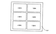
図10はマザーパネルMPから切り出す各パネルの位置(アドレス)を説明する模式図である。マザーパネルMPから6枚のパネルを切り出すものとし、図10に示すように連番によるアドレスが指定されているものとする。「0番地」に対応する位置から切り出したパネルを用いて液晶表示パネル10を製造する場合、この液晶表示パネル10には、末尾5桁の数値を6Nとした識別情報を記録する。他の番地に対応する位置から切り出したパネルを用いて液晶表示パネル10を製造する場合も同様であり、「1番地」〜「5番地」に対応する位置から切り出したパネルを用いて製造した液晶表示パネル10には、それぞれ末尾5桁の数値を6N+1〜6N+5とした識別情報を記録する。
FIG. 10 is a schematic diagram for explaining the position (address) of each panel cut out from the mother panel MP. Assume that six panels are cut out from the mother panel MP, and addresses by serial numbers are designated as shown in FIG. When the liquid
よって、識別情報を参照することにより、その日に切り出されたパネルのうち、何枚目のマザーパネルMPから切り出したパネルであるのか、また、そのマザーパネルMPのどの位置から切り出したパネルであるのかを特定することができる。図11はパネルの特定手法について説明する模式図である。例えば、識別情報の末尾5桁の値がn(ただし、n=6m−5であり、mは自然数)である場合、m枚目のマザーパネルMPの「0番地」に対応する位置から切り出したパネルであると判断することができる。同様に、識別情報の末尾5桁の値がn+1〜n+5である場合、m枚目のマザーパネルMPの「1番地」〜「5番地」に対応する位置から切り出したパネルであると判断することができる。
更に、識別情報の末尾5桁の値がn+6(=6m+1)である場合、m+1枚目のマザーパネルMPの「0番地」に対応する位置から切り出したパネルであると判断することができ、同様に、識別情報の末尾5桁の値がn+7〜n+11である場合、m+1枚目のマザーパネルMPの「1番地」〜「5番地」に対応する位置から切り出したパネルであると判断することができる。
Therefore, by referring to the identification information, it is determined from which mother panel MP the panel cut out on that day, and from which position of the mother panel MP the panel is cut out. Can be specified. FIG. 11 is a schematic diagram for explaining a panel specifying method. For example, if the last five digits of the identification information are n (where n = 6m-5, m is a natural number), the identification information is cut out from the position corresponding to “address 0” of the mth mother panel MP. It can be determined that it is a panel. Similarly, when the last five digits of the identification information are n + 1 to n + 5, it is determined that the panel is cut out from the position corresponding to “address 1” to “
Further, when the last five digits of the identification information are n + 6 (= 6m + 1), it can be determined that the panel is cut out from the position corresponding to “address 0” of the m + 1th mother panel MP. When the last five digits of the identification information are n + 7 to n + 11, it is determined that the panel is cut out from the position corresponding to “address 1” to “
以上のように、液晶表示パネル10に記録する識別情報には、液晶表示パネル10の生産日、その生産日における生産枚数、及びマザーパネルMPから切り出す各パネルの位置(アドレス)の情報を含めることができる。よって、識別情報を参照することにより、マザーパネルMPから切り出したそれぞれのパネルが、どのマザーパネルMPから切り出したものであるのか、マザーパネルMPのどの位置から切り出したものであるのかを特定することができる。
As described above, the identification information recorded on the liquid
このため、例えば、識別情報を参照して、同一のマザーパネルMPから切り出したパネルより製造した複数の液晶表示パネル10,10,…を選択することにより、実施の形態1及び2に記載したマルチディスプレイ装置を製造することができる。また、識別情報を参照して、同一のマザーパネルMPから切り出したパネルのアドレスを特定し、マルチディスプレイ装置における各液晶表示パネル10,10の配置が元のマザーパネルMPにおける各パネルの配置と同じになるように、液晶表示パネル10,10を選択することにより、実施の形態3に記載したマルチディスプレイ装置を製造することができる。
Therefore, for example, by referring to the identification information, by selecting a plurality of liquid
また、製造する液晶表示パネル10のサイズが変更になった場合、アドレスの割り当てを変更してもよい。図12は液晶表示パネル10のサイズ変更に伴うアドレスの割当例を示す模式図である。
Further, when the size of the liquid
なお、各液晶表示パネル10の上下左右は、カラーフィルタ16の配列により確認することができるため、各液晶表示パネル10に記録する識別情報は、各液晶表示パネル10の上下左右の情報を持つ必要はない。カラーフィルタ16の配列は、液晶表示パネル10に向かって、左側よりR,G,Bとなるので、この配列となるように各液晶表示パネル10を配置することにより、液晶表示パネル10の上下左右を揃えることができる。
In addition, since the top, bottom, left, and right of each liquid
実施の形態4では、識別情報をTFT側ガラス基板11の周縁部に記録する構成としたが、識別情報を記録する位置はTFT側ガラス基板11の周縁部に限定されるものではない。例えば、図8に示すように、各液晶表示パネル10の周囲にはブラックマトリクス51が設けられているので、外部から視認可能なブラックマトリクス51の箇所に赤外線又は紫外線を反射するインクで識別情報を記録する構成としてもよい。赤外線を反射するインクとしては、例えば、ITO(酸化インジウムスズ)やATO(酸化アンチモンスズ)の微粒子を含むインクを用いることができる。また、紫外線を反射するインクとしては、ユーロピウム系錯体の発光化合物を含むインクを用いることができる。
In
実施の形態4では、液晶表示パネル10の識別情報として英数字からなる記号を用いたが、必ずしも英数字からなる記号である必要はない。例えば、バーコード又は2次元バーコード等のコードを用いて識別情報を記録する構成としてもよい。
また、実施の形態4では、識別情報として、生産年月日と日毎の生産枚数を表す連番とからなる記号を用いたが、各液晶表示パネル10の出処を識別できる情報であれば、どのような情報を用いてもよい。
In the fourth embodiment, a symbol composed of alphanumeric characters is used as identification information of the liquid
In the fourth embodiment, as the identification information, a symbol composed of a production date and a serial number representing the number of productions per day is used. However, any information can be used as long as it can identify the origin of each liquid
実施の形態5.
実施の形態4では、液晶表示パネル10の外観部分に識別情報を記録する構成としたが、メモリなどの記憶手段に識別情報を記憶させる構成としてもよい。
In the fourth embodiment, the identification information is recorded on the appearance portion of the liquid
各液晶表示パネル10は、制御系の構成として、LCDタイミングコントローラ105及びソースドライバ106を備える(図2を参照)。これらのLCDタイミングコントローラ105及びソースドライバ106は、内蔵のフラッシュメモリを備えており(不図示)、フラッシュメモリに格納された設定値を参照して各種制御を行う。
Each liquid
LCDタイミングコントローラ105及びソースドライバ106は、液晶表示パネル10毎に設けられているので、LCDタイミングコントローラ105又はソースドライバ106に内蔵されたフラッシュメモリの空き容量を利用して、実施の形態4で説明したような識別情報を記憶させることができる。また、フラッシュメモリに記憶させた識別情報は、ROMライタなどの読取装置をコネクタに接続することにより読み出すことが可能である。
Since the
また、各液晶表示パネル10を遠隔操作するためのリモートコントローラを利用して、識別情報の読み出しを実行し、読み出した識別情報を各液晶表示パネル10に表示させる構成としてもよい。
更に、識別情報を記録したICチップ(不図示)をソースドライバ106に組み込み、ICチップとの無線通信により、識別情報を読み出す構成としてもよい。
Alternatively, the remote controller for remotely operating each liquid
Further, an IC chip (not shown) in which identification information is recorded may be incorporated in the
また、液晶表示パネル10には直接的に識別情報を記録せずに、マルチディスプレイ装置単位で、使用している液晶表示パネル10の識別情報を管理する構成としてもよい。例えば、マルチディスプレイ装置毎に割り当てるロット番号に対応付けて、各液晶表示パネル10,10,…の識別情報及び各液晶表示パネル10,10,…の配置に関する情報を管理する構成としてもよい。このようなロット番号は、一般的に、トレーサビリティの観点から、各製品(マルチディスプレイ装置)に付与されている。
Further, the identification information of the liquid
10 液晶表示パネル
11 TFT側ガラス基板
12 TFT
13 画素電極
14,18 配向膜
15 CF側ガラス基板
16 カラーフィルタ
17 対向電極
20 液晶層
30 バックライトユニット
31 拡散板
32,33 偏光板
40 保護ガラス
10 Liquid
13
本発明に係るマルチディスプレイ装置は、複数の液晶表示パネルを、間隔を隔てて並置してあり、入力された映像を分割して各液晶表示パネル用の映像信号を生成し、生成した映像信号に基づく映像を各液晶表示パネルに表示させることによって前記入力された映像を表示するマルチディスプレイ装置において、前記複数の液晶表示パネルのうち少なくとも2つは、液晶物質を封入するための空隙が形成された一のパネル部材から切り出して製造したものであることを特徴とする。 In the multi-display device according to the present invention, a plurality of liquid crystal display panels are juxtaposed at intervals, and an input video is divided to generate a video signal for each liquid crystal display panel. In the multi-display device for displaying the input image by displaying the image based on each liquid crystal display panel, at least two of the plurality of liquid crystal display panels are formed with gaps for enclosing the liquid crystal material It is manufactured by cutting out from one panel member.
本発明に係るマルチディスプレイ装置は、各液晶表示パネルには、該液晶表示パネルを切り出したパネル部材を特定するための情報を記録してあることを特徴とする。
また、本発明に係るマルチディスプレイ装置は、各液晶表示パネルには、該液晶表示パネルを切り出したパネル部材上の位置を特定する情報と、該パネル部材を特定する情報とを、一の連番により表した情報として記録してあることを特徴とする。
The multi-display device according to the present invention is characterized in that information for specifying a panel member from which the liquid crystal display panel is cut out is recorded in each liquid crystal display panel.
Further, in the multi-display device according to the present invention, each liquid crystal display panel is provided with information for specifying the position on the panel member from which the liquid crystal display panel is cut out and information for specifying the panel member. It is recorded as information expressed by the following.
本発明に係るマルチディスプレイ装置の製造方法は、複数の液晶表示パネルを、間隔を隔てて並置してあり、入力された映像を分割して各液晶表示パネル用の映像信号を生成し、生成した映像信号に基づく映像を各液晶表示パネルに表示させることによって前記入力された映像を表示するマルチディスプレイ装置の製造方法において、前記複数の液晶表示パネルのうちの少なくとも2つを、液晶物質を封入するための空隙が形成された一のパネル部材から切り出して製造し、前記一のパネル部材から切り出して製造した少なくとも2つの液晶表示パネルを並置することを特徴とする。 In the method for manufacturing a multi-display device according to the present invention, a plurality of liquid crystal display panels are juxtaposed at intervals, and an input image is divided to generate a video signal for each liquid crystal display panel. In a method of manufacturing a multi-display device that displays an input image by displaying an image based on an image signal on each liquid crystal display panel, at least two of the plurality of liquid crystal display panels are encapsulated with a liquid crystal material. And a liquid crystal display panel cut out from the one panel member and manufactured. The liquid crystal display panel cut out from the one panel member is juxtaposed.
Claims (5)
前記複数の液晶表示パネルのうち少なくとも2つは、液晶物質を封入するための空隙が形成された一のパネル部材から切り出して製造したものであることを特徴とするマルチディスプレイ装置。 In a multi-display device that juxtaposes a plurality of liquid crystal display panels and displays an image on each liquid crystal display panel based on an input video signal,
At least two of the plurality of liquid crystal display panels are manufactured by cutting out one panel member in which a gap for enclosing a liquid crystal material is formed.
前記複数の液晶表示パネルのうちの少なくとも2つを、液晶物質を封入するための空隙が形成された一のパネル部材から切り出して製造し、
前記一のパネル部材から切り出して製造した少なくとも2つの液晶表示パネルを並置する
ことを特徴とするマルチディスプレイ装置の製造方法。 In a method for manufacturing a multi-display device in which a plurality of liquid crystal display panels are juxtaposed, and an image is displayed on each liquid crystal display panel based on an input video signal,
At least two of the plurality of liquid crystal display panels are manufactured by cutting out one panel member in which a gap for enclosing a liquid crystal material is formed,
A method for manufacturing a multi-display device, comprising arranging at least two liquid crystal display panels cut out from the one panel member.
Priority Applications (4)
| Application Number | Priority Date | Filing Date | Title |
|---|---|---|---|
| JP2012144509A JP2014010169A (en) | 2012-06-27 | 2012-06-27 | Multi-display device and method for manufacturing multi-display device |
| CN201380033890.XA CN104508543A (en) | 2012-06-27 | 2013-06-03 | Multi display device |
| PCT/JP2013/065363 WO2014002694A1 (en) | 2012-06-27 | 2013-06-03 | Multi display device |
| US14/410,165 US20150370112A1 (en) | 2012-06-27 | 2013-06-03 | Multi-display apparatus |
Applications Claiming Priority (1)
| Application Number | Priority Date | Filing Date | Title |
|---|---|---|---|
| JP2012144509A JP2014010169A (en) | 2012-06-27 | 2012-06-27 | Multi-display device and method for manufacturing multi-display device |
Publications (1)
| Publication Number | Publication Date |
|---|---|
| JP2014010169A true JP2014010169A (en) | 2014-01-20 |
Family
ID=49782860
Family Applications (1)
| Application Number | Title | Priority Date | Filing Date |
|---|---|---|---|
| JP2012144509A Pending JP2014010169A (en) | 2012-06-27 | 2012-06-27 | Multi-display device and method for manufacturing multi-display device |
Country Status (4)
| Country | Link |
|---|---|
| US (1) | US20150370112A1 (en) |
| JP (1) | JP2014010169A (en) |
| CN (1) | CN104508543A (en) |
| WO (1) | WO2014002694A1 (en) |
Cited By (2)
| Publication number | Priority date | Publication date | Assignee | Title |
|---|---|---|---|---|
| KR20190032109A (en) * | 2017-09-19 | 2019-03-27 | 에스케이텔레콤 주식회사 | Image display method |
| JP2019204066A (en) * | 2018-05-25 | 2019-11-28 | パナソニックIpマネジメント株式会社 | Lens barrel module |
Families Citing this family (5)
| Publication number | Priority date | Publication date | Assignee | Title |
|---|---|---|---|---|
| KR102507472B1 (en) * | 2016-02-26 | 2023-03-09 | 삼성전자주식회사 | Antenna in Electronic Device with Display |
| ITUA20163400A1 (en) | 2016-05-12 | 2017-11-12 | Alberto Rolla | Optical recognition system of capsules for the production of hot drinks |
| KR102111045B1 (en) * | 2017-10-31 | 2020-05-14 | 엘지디스플레이 주식회사 | Display device |
| CN111916017A (en) * | 2020-08-18 | 2020-11-10 | 紫旸升光电科技(苏州)有限公司 | Double-display-screen color correction method and correction system |
| CN113342369A (en) * | 2021-05-11 | 2021-09-03 | 中天恒星(上海)科技有限公司 | Display card configuration method and main board |
Citations (7)
| Publication number | Priority date | Publication date | Assignee | Title |
|---|---|---|---|---|
| JPS6324283A (en) * | 1986-07-16 | 1988-02-01 | 株式会社精工舎 | Liquid crystal display panel |
| JPH1096911A (en) * | 1996-07-09 | 1998-04-14 | Lg Electron Inc | High-density large-sized screen liquid crystal display device and its production |
| JP2001109392A (en) * | 1999-10-05 | 2001-04-20 | Matsushita Electric Ind Co Ltd | Production method of device |
| JP2007025670A (en) * | 2005-07-12 | 2007-02-01 | Samsung Electronics Co Ltd | Mother board for display device and method for manufacturing the same |
| JP2007108590A (en) * | 2005-10-17 | 2007-04-26 | Sony Corp | Liquid crystal display panel, imparting method of step identifier of liquid crystal display panel and defect specifying method of liquid crystal display panel |
| JP2008083701A (en) * | 2006-09-25 | 2008-04-10 | Samsung Electronics Co Ltd | Multi-display apparatus and manufacturing method therefor |
| JP2012037628A (en) * | 2010-08-04 | 2012-02-23 | Sharp Corp | Multi-display system |
Family Cites Families (1)
| Publication number | Priority date | Publication date | Assignee | Title |
|---|---|---|---|---|
| US8080926B2 (en) * | 2006-09-25 | 2011-12-20 | Samsung Electronics Co., Ltd. | Multi-display apparatus and method of manufacturing the same |
-
2012
- 2012-06-27 JP JP2012144509A patent/JP2014010169A/en active Pending
-
2013
- 2013-06-03 WO PCT/JP2013/065363 patent/WO2014002694A1/en active Application Filing
- 2013-06-03 US US14/410,165 patent/US20150370112A1/en not_active Abandoned
- 2013-06-03 CN CN201380033890.XA patent/CN104508543A/en active Pending
Patent Citations (7)
| Publication number | Priority date | Publication date | Assignee | Title |
|---|---|---|---|---|
| JPS6324283A (en) * | 1986-07-16 | 1988-02-01 | 株式会社精工舎 | Liquid crystal display panel |
| JPH1096911A (en) * | 1996-07-09 | 1998-04-14 | Lg Electron Inc | High-density large-sized screen liquid crystal display device and its production |
| JP2001109392A (en) * | 1999-10-05 | 2001-04-20 | Matsushita Electric Ind Co Ltd | Production method of device |
| JP2007025670A (en) * | 2005-07-12 | 2007-02-01 | Samsung Electronics Co Ltd | Mother board for display device and method for manufacturing the same |
| JP2007108590A (en) * | 2005-10-17 | 2007-04-26 | Sony Corp | Liquid crystal display panel, imparting method of step identifier of liquid crystal display panel and defect specifying method of liquid crystal display panel |
| JP2008083701A (en) * | 2006-09-25 | 2008-04-10 | Samsung Electronics Co Ltd | Multi-display apparatus and manufacturing method therefor |
| JP2012037628A (en) * | 2010-08-04 | 2012-02-23 | Sharp Corp | Multi-display system |
Cited By (5)
| Publication number | Priority date | Publication date | Assignee | Title |
|---|---|---|---|---|
| KR20190032109A (en) * | 2017-09-19 | 2019-03-27 | 에스케이텔레콤 주식회사 | Image display method |
| WO2019059633A1 (en) * | 2017-09-19 | 2019-03-28 | 에스케이텔레콤 주식회사 | Image display method |
| KR101979410B1 (en) * | 2017-09-19 | 2019-05-16 | 에스케이텔레콤 주식회사 | Image display method |
| US11175874B2 (en) | 2017-09-19 | 2021-11-16 | Sk Telecom Co., Ltd. | Image display method |
| JP2019204066A (en) * | 2018-05-25 | 2019-11-28 | パナソニックIpマネジメント株式会社 | Lens barrel module |
Also Published As
| Publication number | Publication date |
|---|---|
| US20150370112A1 (en) | 2015-12-24 |
| CN104508543A (en) | 2015-04-08 |
| WO2014002694A1 (en) | 2014-01-03 |
Similar Documents
| Publication | Publication Date | Title |
|---|---|---|
| WO2014002694A1 (en) | Multi display device | |
| CN106297626B (en) | Multi-view display device | |
| CN105892138B (en) | transparent liquid crystal display | |
| WO2018010251A1 (en) | Foldable liquid crystal display and manufacturing method therefor | |
| KR101295884B1 (en) | Multi view and stereoscopic image display | |
| US20120154711A1 (en) | Transparent liquid crystal display device | |
| CN101571631A (en) | Liquid crystal display module and liquid crystal display panel | |
| JP2007248699A (en) | Electrooptic device and electronic equipment | |
| US9995966B2 (en) | Display panel and display apparatus having retardation film with grid | |
| US20190129208A1 (en) | Transparent display system and display method thereof | |
| TW201346343A (en) | A patterned retarder type display device having black strips and manufacturing method therefor | |
| CN104570464B (en) | Large scale display device | |
| US20140347614A1 (en) | Liquid crystal display device | |
| JP2013214070A (en) | Display panel and display device including the same | |
| JP2013041100A (en) | Transparent display device | |
| JP2008164702A (en) | Display element and its manufacturing method | |
| WO2021056692A1 (en) | Display panel and method for manufacturing same, and display apparatus | |
| KR20140059547A (en) | Transparent display apparatus and method for controlling thereof | |
| US20160266447A1 (en) | Liquid crystal lens panel and display device including liquid crystal lens panel | |
| JP2015138217A (en) | Electro-optical device and electronic apparatus | |
| JP2013501960A (en) | Manufacturing method of multi-display device | |
| KR102633411B1 (en) | Back Light Unit and Liquid Crystal Display Device using the same | |
| JP2019200372A (en) | Liquid crystal device and electronic apparatus | |
| CN220208035U (en) | Display module and display device | |
| KR101267085B1 (en) | Multi view display |
Legal Events
| Date | Code | Title | Description |
|---|---|---|---|
| A131 | Notification of reasons for refusal |
Free format text: JAPANESE INTERMEDIATE CODE: A131 Effective date: 20140318 |
|
| A521 | Written amendment |
Free format text: JAPANESE INTERMEDIATE CODE: A523 Effective date: 20140513 |
|
| A02 | Decision of refusal |
Free format text: JAPANESE INTERMEDIATE CODE: A02 Effective date: 20141111 |