JP2013541854A - Optical elements for vertical external cavity surface emitting lasers. - Google Patents
Optical elements for vertical external cavity surface emitting lasers. Download PDFInfo
- Publication number
- JP2013541854A JP2013541854A JP2013537237A JP2013537237A JP2013541854A JP 2013541854 A JP2013541854 A JP 2013541854A JP 2013537237 A JP2013537237 A JP 2013537237A JP 2013537237 A JP2013537237 A JP 2013537237A JP 2013541854 A JP2013541854 A JP 2013541854A
- Authority
- JP
- Japan
- Prior art keywords
- vecsel
- optical
- mirror
- substrate
- interface
- Prior art date
- Legal status (The legal status is an assumption and is not a legal conclusion. Google has not performed a legal analysis and makes no representation as to the accuracy of the status listed.)
- Pending
Links
Images


Classifications
-
- H—ELECTRICITY
- H01—ELECTRIC ELEMENTS
- H01S—DEVICES USING THE PROCESS OF LIGHT AMPLIFICATION BY STIMULATED EMISSION OF RADIATION [LASER] TO AMPLIFY OR GENERATE LIGHT; DEVICES USING STIMULATED EMISSION OF ELECTROMAGNETIC RADIATION IN WAVE RANGES OTHER THAN OPTICAL
- H01S5/00—Semiconductor lasers
- H01S5/10—Construction or shape of the optical resonator, e.g. extended or external cavity, coupled cavities, bent-guide, varying width, thickness or composition of the active region
- H01S5/18—Surface-emitting [SE] lasers, e.g. having both horizontal and vertical cavities
- H01S5/183—Surface-emitting [SE] lasers, e.g. having both horizontal and vertical cavities having only vertical cavities, e.g. vertical cavity surface-emitting lasers [VCSEL]
- H01S5/18361—Structure of the reflectors, e.g. hybrid mirrors
-
- G—PHYSICS
- G02—OPTICS
- G02B—OPTICAL ELEMENTS, SYSTEMS OR APPARATUS
- G02B19/00—Condensers, e.g. light collectors or similar non-imaging optics
- G02B19/0033—Condensers, e.g. light collectors or similar non-imaging optics characterised by the use
- G02B19/0047—Condensers, e.g. light collectors or similar non-imaging optics characterised by the use for use with a light source
- G02B19/0052—Condensers, e.g. light collectors or similar non-imaging optics characterised by the use for use with a light source the light source comprising a laser diode
- G02B19/0057—Condensers, e.g. light collectors or similar non-imaging optics characterised by the use for use with a light source the light source comprising a laser diode in the form of a laser diode array, e.g. laser diode bar
-
- H—ELECTRICITY
- H01—ELECTRIC ELEMENTS
- H01S—DEVICES USING THE PROCESS OF LIGHT AMPLIFICATION BY STIMULATED EMISSION OF RADIATION [LASER] TO AMPLIFY OR GENERATE LIGHT; DEVICES USING STIMULATED EMISSION OF ELECTROMAGNETIC RADIATION IN WAVE RANGES OTHER THAN OPTICAL
- H01S5/00—Semiconductor lasers
- H01S5/02—Structural details or components not essential to laser action
- H01S5/026—Monolithically integrated components, e.g. waveguides, monitoring photo-detectors, drivers
- H01S5/0267—Integrated focusing lens
-
- H—ELECTRICITY
- H01—ELECTRIC ELEMENTS
- H01S—DEVICES USING THE PROCESS OF LIGHT AMPLIFICATION BY STIMULATED EMISSION OF RADIATION [LASER] TO AMPLIFY OR GENERATE LIGHT; DEVICES USING STIMULATED EMISSION OF ELECTROMAGNETIC RADIATION IN WAVE RANGES OTHER THAN OPTICAL
- H01S5/00—Semiconductor lasers
- H01S5/40—Arrangement of two or more semiconductor lasers, not provided for in groups H01S5/02 - H01S5/30
- H01S5/4025—Array arrangements, e.g. constituted by discrete laser diodes or laser bar
- H01S5/4031—Edge-emitting structures
- H01S5/4062—Edge-emitting structures with an external cavity or using internal filters, e.g. Talbot filters
-
- H—ELECTRICITY
- H01—ELECTRIC ELEMENTS
- H01S—DEVICES USING THE PROCESS OF LIGHT AMPLIFICATION BY STIMULATED EMISSION OF RADIATION [LASER] TO AMPLIFY OR GENERATE LIGHT; DEVICES USING STIMULATED EMISSION OF ELECTROMAGNETIC RADIATION IN WAVE RANGES OTHER THAN OPTICAL
- H01S5/00—Semiconductor lasers
- H01S5/40—Arrangement of two or more semiconductor lasers, not provided for in groups H01S5/02 - H01S5/30
- H01S5/42—Arrays of surface emitting lasers
- H01S5/423—Arrays of surface emitting lasers having a vertical cavity
-
- H—ELECTRICITY
- H01—ELECTRIC ELEMENTS
- H01S—DEVICES USING THE PROCESS OF LIGHT AMPLIFICATION BY STIMULATED EMISSION OF RADIATION [LASER] TO AMPLIFY OR GENERATE LIGHT; DEVICES USING STIMULATED EMISSION OF ELECTROMAGNETIC RADIATION IN WAVE RANGES OTHER THAN OPTICAL
- H01S3/00—Lasers, i.e. devices using stimulated emission of electromagnetic radiation in the infrared, visible or ultraviolet wave range
- H01S3/05—Construction or shape of optical resonators; Accommodation of active medium therein; Shape of active medium
- H01S3/08—Construction or shape of optical resonators or components thereof
- H01S3/08059—Constructional details of the reflector, e.g. shape
-
- H—ELECTRICITY
- H01—ELECTRIC ELEMENTS
- H01S—DEVICES USING THE PROCESS OF LIGHT AMPLIFICATION BY STIMULATED EMISSION OF RADIATION [LASER] TO AMPLIFY OR GENERATE LIGHT; DEVICES USING STIMULATED EMISSION OF ELECTROMAGNETIC RADIATION IN WAVE RANGES OTHER THAN OPTICAL
- H01S5/00—Semiconductor lasers
- H01S5/02—Structural details or components not essential to laser action
- H01S5/026—Monolithically integrated components, e.g. waveguides, monitoring photo-detectors, drivers
-
- H—ELECTRICITY
- H01—ELECTRIC ELEMENTS
- H01S—DEVICES USING THE PROCESS OF LIGHT AMPLIFICATION BY STIMULATED EMISSION OF RADIATION [LASER] TO AMPLIFY OR GENERATE LIGHT; DEVICES USING STIMULATED EMISSION OF ELECTROMAGNETIC RADIATION IN WAVE RANGES OTHER THAN OPTICAL
- H01S5/00—Semiconductor lasers
- H01S5/10—Construction or shape of the optical resonator, e.g. extended or external cavity, coupled cavities, bent-guide, varying width, thickness or composition of the active region
- H01S5/14—External cavity lasers
-
- H—ELECTRICITY
- H01—ELECTRIC ELEMENTS
- H01S—DEVICES USING THE PROCESS OF LIGHT AMPLIFICATION BY STIMULATED EMISSION OF RADIATION [LASER] TO AMPLIFY OR GENERATE LIGHT; DEVICES USING STIMULATED EMISSION OF ELECTROMAGNETIC RADIATION IN WAVE RANGES OTHER THAN OPTICAL
- H01S5/00—Semiconductor lasers
- H01S5/10—Construction or shape of the optical resonator, e.g. extended or external cavity, coupled cavities, bent-guide, varying width, thickness or composition of the active region
- H01S5/18—Surface-emitting [SE] lasers, e.g. having both horizontal and vertical cavities
- H01S5/183—Surface-emitting [SE] lasers, e.g. having both horizontal and vertical cavities having only vertical cavities, e.g. vertical cavity surface-emitting lasers [VCSEL]
- H01S5/18386—Details of the emission surface for influencing the near- or far-field, e.g. a grating on the surface
- H01S5/18388—Lenses
Abstract
本発明は、VECSEL又はVECSELアレイに対する光学素子に関する。前記光学素子は、少なくとも光学放射線の波長領域において透明である基板200で形成される。基板200の第1の界面は、基板200に一体化された光学レンズ又は光学レンズ220のアレイの一部を形成する1つ又は複数の湾曲領域を有する。基板200は、前記第1の界面の反対側の基板200の第2の界面に形成された又は基板200に埋め込まれた1つ又は複数の光学鏡210を有する。光学鏡210は、前記第1の又は第2の界面に入射する光学放射線の一部を後方反射するように配置及び設計される。光学鏡210は、平面鏡又は湾曲領域220の曲率半径とは異なる曲率半径を持つ曲面鏡である。前記光学素子は、製造中の追加の調整の必要性なしで高輝度を持つVECSEL又はVECSELアレイの製造を可能にする。前記VECSELは、光学鏡210に対する距離Lに配置され、これは、外部キャビティの長さに等しい。前記光学レンズのROCは、ROC=L/2に選択されることがありえ、前記光学鏡に対してROC>Lである。前記キャビティ長さは、モノリシックスペーサ120により調整されうる。 The present invention relates to optical elements for VECSEL or VECSEL arrays. The optical element is formed of a substrate 200 that is transparent at least in the wavelength region of optical radiation. The first interface of the substrate 200 has one or more curved regions that form part of an array of optical lenses or optical lenses 220 that are integrated with the substrate 200. The substrate 200 has one or more optical mirrors 210 formed at or embedded in the second interface of the substrate 200 opposite the first interface. The optical mirror 210 is arranged and designed to back reflect a portion of the optical radiation incident on the first or second interface. The optical mirror 210 is a plane mirror or a curved mirror having a curvature radius different from the curvature radius of the curved region 220. The optical element enables the production of high brightness VECSEL or VECSEL arrays without the need for additional adjustments during manufacture. The VECSEL is placed at a distance L relative to the optical mirror 210, which is equal to the length of the external cavity. The ROC of the optical lens may be selected as ROC = L / 2, where ROC> L with respect to the optical mirror. The cavity length can be adjusted by the monolithic spacer 120.
Description
本発明は、少なくとも光学的放射線の波長領域において透明である基板で形成される光学素子に関し、前記基板の第1の界面は、前記基板に一体化された光学レンズ又は光学レンズのアレイの一部を形成する1つ又は複数の湾曲領域を有する。本発明は、前記レーザの発光側に配置されたこのような光学素子を持つ垂直外部キャビティ面発光レーザ(VECSEL、vertical external-cavity surface-emitting laser)にも関する。 The present invention relates to an optical element formed of a substrate that is transparent at least in the wavelength region of optical radiation, wherein the first interface of the substrate is part of an optical lens or an array of optical lenses integrated with the substrate. Having one or more curved regions. The invention also relates to a vertical external-cavity surface-emitting laser (VECSEL) having such an optical element arranged on the light-emitting side of the laser.
VECSELは、最も期待できる高輝度レーザ光源の1つであり、エッジエミッタと比較して、アドレス可能な2Dアレイ構成及び円形ビーム形状のような、多くの利点を提供する。標準的なセットアップにおいて、外部キャビティは、非常に大きくかつ洗練された調整を必要とする巨視的な光学素子からなる。ウエハ上で外部光学部品を実現し、このウエハを、前記VECSELの半導体部品を持っているGaAsウエハに結合することにより、数千のマイクロVECSELを並列に製造し、VCSEL(垂直キャビティ面発光レーザ)のように前記ウエハ上で直接的にこれらを試験することが可能である。G.A. Keeler et al. "Single Transverse Mode Operation of Electrically Pumped Vertical-External-Cavity Surface-Emitting Lasers with Micromirrors", IEEE Photonics Technology Letters, Vol. 17, No. 3, March 2005, pp 522-524は、マイクロモールディングを使用するガラス基板上のマイクロミラーの製造を記載しており、前記基板は、屈折率整合光学エポキシを持つGaAsウエハに結合される。このようなマイクロVECSELは、良好な性能(1に近いM2)を示す。 VECSEL is one of the most promising high-brightness laser light sources and offers many advantages over edge emitters, such as addressable 2D array configuration and circular beam shape. In a standard setup, the external cavity consists of macroscopic optics that require very large and sophisticated adjustments. External optical parts are realized on the wafer, and this wafer is bonded to a GaAs wafer having the VECSEL semiconductor parts, thereby producing thousands of micro VECSELs in parallel. VCSEL (Vertical Cavity Surface Emitting Laser) It is possible to test these directly on the wafer. GA Keeler et al. "Single Transverse Mode Operation of Electrically Pumped Vertical-External-Cavity Surface-Emitting Lasers with Micromirrors", IEEE Photonics Technology Letters, Vol. 17, No. 3, March 2005, pp 522-524 Describes the fabrication of micromirrors on glass substrates, which are bonded to a GaAs wafer with a refractive index matching optical epoxy. Such micro-VECSEL shows good performance (M 2 close to 1).
前記VECSELの外部キャビティは、半導体ウエハに結合された光学的に透明な基板上の球面鏡により規定される。パワーを高めるために、複数のVECSELが、アレイに配置されることができる。熱的な理由で、多数の小さな装置は、少数の大きな装置より適している。小さな作動直径(active diameter)、したがって小さなビームウエストは、高い発散角を意味し、このようなアレイの輝度を低減させる。発散角を低下させるために、マイクロレンズアレイが、各VECSELの放射線をコリメートし、したがって、ビームパラメータプロダクト(beam parameter product)を低下させ、前記VECSELアレイの輝度を増大させるのに使用されることができる。しかしながら、積み重ねられた光学透明ウエハが使用される場合、チップレベル又はウエハレベルのいずれかで、追加の調整ステップが、このレンズに対して必要である。 The external cavity of the VECSEL is defined by a spherical mirror on an optically transparent substrate bonded to a semiconductor wafer. Multiple VECSELs can be placed in the array to increase power. For thermal reasons, many small devices are more suitable than a few large devices. A small active diameter, and thus a small beam waist, means a high divergence angle and reduces the brightness of such an array. In order to reduce the divergence angle, a microlens array is used to collimate the radiation of each VECSEL, thus reducing the beam parameter product and increasing the brightness of the VECSEL array. it can. However, if stacked optically transparent wafers are used, additional adjustment steps are required for this lens, either at the chip level or at the wafer level.
本発明の目的は、製造中の追加の調整ステップの必要性なしでVECSELの輝度を増大させるVECSEL又はVECSELアレイを製造する手段を提供することである。 It is an object of the present invention to provide a means of manufacturing a VECSEL or VECSEL array that increases the brightness of the VECSEL without the need for additional adjustment steps during manufacture.
この目的は、請求項1に記載の光学素子で達成される。請求項6は、このような光学素子を有するVECSEL(アレイ)を記載する。この光学素子又はVECSELアレイの有利な実施例は、従属請求項の対象であるか、又は明細書の後の部分に記載される。 This object is achieved with the optical element according to claim 1. Claim 6 describes a VECSEL (array) having such an optical element. Advantageous embodiments of this optical element or VECSEL array are the subject of the dependent claims or are described later in the specification.
提案される光学素子は、少なくとも光学放射線の波長範囲内の波長領域において透明である基板で形成される。本特許出願において、光学放射線は、赤外(IR)、可視(VIS)及び紫外(UV)波長範囲の電磁放射線を意味する。前記基板は、前記光学素子が設計される対応するVECSELがレーザ放射線を放射する波長領域においてのみ透明でなければならない。前記基板の第1の界面は、前記基板に一体化された光学レンズ又は光学レンズのアレイ、特にマイクロレンズの一部を形成する1つ又は複数の湾曲領域を有する。前記基板は、前記第1の界面の反対側の前記基板の第2の界面上に形成された又は前記第1の界面に実質的に平行な面において前記基板に埋め込まれた1つ又は複数の光学鏡を有する。前記1つ又は複数の光学鏡は、前記第1の又は第2の界面に入射する前記波長領域の光学放射線の一部を後方反射するように配置及び設計される。この構成は、90°の角度で入射する前記波長領域の光学放射線が、部分的に前記対応する光学鏡により後方反射されるのに対し、残りの部分は、前記基板において前記鏡の後ろに形成された前記レンズを通過する。このために、前記鏡の反射率は、好ましくは、所望の波長領域において30%ないし99.5%である。前記1つ又は複数の光学鏡は、平面鏡又は前記光学レンズを形成する前記1つ又は複数の湾曲領域の曲率半径とは異なる曲率半径を持つ湾曲鏡である。 The proposed optical element is formed of a substrate that is transparent at least in the wavelength region within the wavelength range of optical radiation. In this patent application, optical radiation means electromagnetic radiation in the infrared (IR), visible (VIS) and ultraviolet (UV) wavelength ranges. The substrate must be transparent only in the wavelength region where the corresponding VECSEL on which the optical element is designed emits laser radiation. The first interface of the substrate has one or more curved regions forming part of an optical lens or an array of optical lenses integrated in the substrate, in particular a microlens. The substrate is formed on a second interface of the substrate opposite the first interface or embedded in the substrate in a plane substantially parallel to the first interface. Has an optical mirror. The one or more optical mirrors are arranged and designed to back reflect a portion of the optical radiation in the wavelength region that is incident on the first or second interface. In this configuration, optical radiation in the wavelength region incident at an angle of 90 ° is partially reflected back by the corresponding optical mirror, while the remaining portion is formed behind the mirror in the substrate. Pass through the lens. For this, the reflectivity of the mirror is preferably between 30% and 99.5% in the desired wavelength region. The one or more optical mirrors are curved mirrors having a radius of curvature different from a radius of curvature of the one or more curved regions forming the plane mirror or the optical lens.
前記光学素子の鏡が前記VECSELの外部鏡を形成するVECSEL又はVECSELアレイの一部としてこのような光学素子を使用すると、前記鏡を通るレーザ放射線は、前記光学レンズによりコリメートされることができ、したがって、前記VECSELのより高い輝度を可能にする。 Using such an optical element as part of a VECSEL or VECSEL array where the mirror of the optical element forms an external mirror of the VECSEL, laser radiation passing through the mirror can be collimated by the optical lens; Therefore, higher brightness of the VECSEL is possible.
本発明は、したがって、VECSELの外部鏡及び単一の基板、好ましくはガラス基板上のコリメーションレンズの組み合わせを使用することを提案する。このような光学素子は、例えば以下のように製造されることができる。第1のステップにおいて、マイクロレンズ、特に球面マイクロレンズは、例えばガラスモールディング、UVモールディング又はRIE転写(RIE:反応性イオンエッチング)により、前記基板上に形成される。反射コーティングは、前記レンズ上に付着され、前記レンズの表面は、前記VECSELの外部マイクロミラーとして機能する。前記反射コーティングは、前記表面の一部しか覆わないこともありえ、すなわちパターニングされうる。これは、例えばモード選択に対して、前記放射線の特別な角度領域のみを後方反射するように機能しうる。第2のステップにおいて、球面マイクロレンズ又は異なる曲率半径(ROC)を持つ非球面マイクロレンズが、前記第1のマイクロレンズの上に、すなわち前記マイクロミラーの上に形成される。この更なるマイクロレンズの表面のROCは、前記VECSELから前記マイクロミラーを通ってくる光がコリメートされるように選択される。このような光学素子は、VECSELの製造中に前記マイクロレンズに対して追加の調整ステップを必要としない。したがって、製造プロセスは単純化される。 The present invention therefore proposes to use a combination of a VECSEL external mirror and a collimation lens on a single substrate, preferably a glass substrate. Such an optical element can be manufactured as follows, for example. In the first step, microlenses, in particular spherical microlenses, are formed on the substrate, for example by glass molding, UV molding or RIE transfer (RIE: reactive ion etching). A reflective coating is deposited on the lens, and the surface of the lens functions as an external micromirror for the VECSEL. The reflective coating may cover only part of the surface, i.e. it may be patterned. This can serve to reflect back only a special angular region of the radiation, for example for mode selection. In the second step, a spherical microlens or an aspherical microlens with a different radius of curvature (ROC) is formed on the first microlens, ie on the micromirror. The ROC on the surface of this further microlens is selected so that light coming from the VECSEL through the micromirror is collimated. Such an optical element does not require an additional adjustment step for the microlens during the manufacture of VECSEL. Therefore, the manufacturing process is simplified.
有利な実施例において、前記光学素子は、例えばウエハ上で、VECSELアレイにおいて使用されることができるマイクロレンズ及びマイクロミラーのアレイを有する。前記光学素子は、前記VECSELの半導体部品を持つ前記基板(キャリア基板)に異なる技術で付着されることができる。前記部品は、例えば、このキャリア基板、例えば半導体基板、又は前記VECSELの半導体部品を形成する層スタックに結合、接着又ははんだ付けされうる。 In an advantageous embodiment, the optical element comprises an array of microlenses and micromirrors that can be used in a VECSEL array, for example on a wafer. The optical element can be attached to the substrate (carrier substrate) having the VECSEL semiconductor component by different techniques. The components can be bonded, glued or soldered, for example, to this carrier substrate, for example a semiconductor substrate, or a layer stack forming the VECSEL semiconductor components.
前記VECSELは、例えば、第1のDBR(分散ブラッグ反射器)と第2のDBRとの間に配置された光学利得媒質を有しうる。前記第2のDBRは、レーザキャビティにおいて共振するレーザ放射線に対して部分的に透明である。前記第2のDBRは、前記外部鏡なしで前記第1のDBRと前記第2のDBRとの間のレージングを可能にしない反射率を持ってもよく、又は前記外部鏡なしで内部レーザキャビティにおけるレージングを可能にする反射率を持ってもよい。前記DBR及び前記利得媒質は、半導体基板、特にGaAs基板上に適切に設計された層スタックから既知のやり方で形成されうる。前記半導体基板を通して放射するVECSELの場合、前記外部鏡を形成する前記光学素子は、この場合に生成されたレーザ放射線に対して光学的に透明でなくてはならないこの基板に付着される。前記VECSELを動作するのに必要な電気接続も、既知のやり方で形成されることができる。 The VECSEL may have, for example, an optical gain medium disposed between a first DBR (Dispersive Bragg Reflector) and a second DBR. The second DBR is partially transparent to laser radiation that resonates in the laser cavity. The second DBR may have a reflectivity that does not allow lasing between the first DBR and the second DBR without the outer mirror, or in the inner laser cavity without the outer mirror. It may have a reflectivity that allows lasing. The DBR and the gain medium can be formed in a known manner from a suitably designed layer stack on a semiconductor substrate, in particular a GaAs substrate. In the case of VECSEL emitting through the semiconductor substrate, the optical elements forming the external mirror are attached to this substrate, which must be optically transparent to the laser radiation generated in this case. The electrical connections necessary to operate the VECSEL can also be made in a known manner.
前記キャリア基板の表面に前記光学素子を直接的に付着する代わりに、前記キャリア基板の表面上に又は前記レーザの隣に取り付けられたスペーサを使用することも可能であり、前記光学素子は、前記スペーサに取り付けられる。前記スペーサは、第一に、前記光学素子の表面に付着されてもよく、又は前記光学素子の製造中にこの表面に一体化されてもよい。このような実施例において、前記光学素子の表面と前記層スタックとの間に空隙が残る。更に、透明なスペーサ層が、前記光学素子と前記キャリア基板との間に付着されうる。このような層は、この素子の製造中に前記光学素子の表面上に既に形成されていてもよい。前記キャリア基板に前記光学素子を付着する代わりに、(エピタキシ側発光VECSEL又はキャリア基板を取り外したVECSELの場合に)前記光学素子は、前記第2のDBR又は下にあるVECSELスタックの他の構造、例えば中間層に、又は前記第2のDBRを省略する場合に前記作動領域上の層上に、付着されることもありうる。前記VECSELの層スタックは、当技術分野において既知の異なるやり方で作成されることができる。 Instead of attaching the optical element directly to the surface of the carrier substrate, it is also possible to use a spacer mounted on the surface of the carrier substrate or next to the laser, the optical element comprising: It is attached to the spacer. The spacer may first be attached to the surface of the optical element or may be integrated into this surface during the manufacture of the optical element. In such an embodiment, an air gap remains between the surface of the optical element and the layer stack. In addition, a transparent spacer layer may be deposited between the optical element and the carrier substrate. Such a layer may already be formed on the surface of the optical element during the manufacture of the element. Instead of attaching the optical element to the carrier substrate, the optical element may be the second DBR or other structure of the underlying VECSEL stack (in the case of epitaxy-side emitting VECSEL or VECSEL with the carrier substrate removed), For example, it may be deposited on an intermediate layer or on a layer on the working area if the second DBR is omitted. The VECSEL layer stack can be made in different ways known in the art.
好適な実施例において、前記光学素子の鏡は、曲面鏡、特に凹面鏡であり、前記マイクロレンズを形成する前記光学素子の前記第1の界面上の湾曲領域の曲率半径は、前記VECSELにより放射されるレーザ放射線をコリメートするように選択される。好ましくは、前記鏡のROCは、前記マイクロレンズの湾曲領域のROCより大きい。それでも、前記マイクロレンズは、他のビーム形成効果を達成するように設計されることもありうる。 In a preferred embodiment, the mirror of the optical element is a curved mirror, in particular a concave mirror, and the radius of curvature of the curved region on the first interface of the optical element forming the microlens is emitted by the VECSEL. Selected to collimate the laser radiation. Preferably, the ROC of the mirror is larger than the ROC of the curved region of the microlens. Nevertheless, the microlenses can be designed to achieve other beamforming effects.
本発明のこれら及び他の態様は、以下に記載される実施例を参照して説明され、明らかになる。 These and other aspects of the invention are apparent from and will be elucidated with reference to the embodiments described hereinafter.
以下の例示的な実施例は、請求項により規定される保護範囲を限定することなしに添付の図面を参照して提案された光学素子及びVECSELの例を示す。 The following exemplary embodiments show examples of proposed optical elements and VECSELs with reference to the accompanying drawings without limiting the scope of protection defined by the claims.
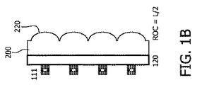
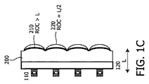
図1は、従来技術の解決法と比べた本発明の光学素子を持つVECSELアレイの一実施例の比較を示す。図1Aは、外部鏡が、光学的に透明なキャリア基板120に付着される光学的に透明な基板200上に形成され、前記VECSELの半導体層スタックが、光学的に透明なキャリア基板120上に結合又は成長される従来技術のVECSELアレイを描く。この構成は、前記キャリア基板を通してレーザ放射線を放射する、いわゆる裏側又は底部発光VCSELに似ている。基板200上の前記外部鏡は、表面を球面(又は非球面)形状(鏡面210)に加工し、この表面上に反射層をコーティングすることにより形成される。前記表面の結果として生じる湾曲領域の曲率半径(ROC)は、条件ROC>Lを満たし、Lは前記VECSELの利得領域に対するこれら外部凹面鏡の距離である。
FIG. 1 shows a comparison of one embodiment of a VECSEL array with an optical element of the present invention compared to a prior art solution. In FIG. 1A, an external mirror is formed on an optically
VCSELの分野において、このようなアレイのVCSEL111のレーザ放射をコリメートするためにマイクロレンズのアレイを使用することが既知である。これらのマイクロレンズは、光学的に透明な基板200において形成され、光学的に透明な基板200の表面が、図1Bに示されるように、前記マイクロレンズの一部を形成する湾曲領域を提供するように球面(又は非球面)形状(レンズ表面220)に加工される。
In the field of VCSELs, it is known to use arrays of microlenses to collimate the laser radiation of such arrays of
図1Cは、本発明による一体化された光学素子を持つ提案されたVECSELアレイの一例を示す。前記光学素子は、反射コーティングを持つ球面(又は非球面)形状表面により形成される一体化されたマイクロミラーと、前記基板表面の球面(又は非球面)形状(レンズ表面220)により前記マイクロミラーの上に形成された一体化されたマイクロレンズとを持つ光学的に透明な基板200を有する。
FIG. 1C shows an example of a proposed VECSEL array with integrated optical elements according to the present invention. The optical element includes an integrated micromirror formed by a spherical (or aspherical) shaped surface having a reflective coating, and a spherical (or aspherical) shape (lens surface 220) of the substrate surface. It has an optically
前記光学素子のこのような構造を達成するために、基板200の表面は、球面又は非球面形状(ミラー表面210)を持つ複数の湾曲領域を持つように加工される。前記基板は、所望の波長領域において光学的に透明な適切な材料で作られ、例えばガラス、ガリウムヒ素、ケイ素等で作られる。ガラス基板を使用する場合、鏡面210の球面形状は、例えばガラスモールディング、RIE転写、機械加工又は熱エンボス加工により達成されることができる。前記基板に異なる材料を付着し、例えばUVレプリケーションにより又はジェット加工を用いる高分子の堆積により、この異なる材料を所望の形状に形成することも、可能である。鏡面210の球面形状のROCは、距離Lにおいて利得媒質を持つVECSELのレーザキャビティのエンドミラーの1つを形成する球面鏡として機能するように選択される。通常、この外部球面鏡のROCは、Lより大きく、好ましくは約2Lである。反射コーティングは、所望の波長領域において典型的には30%ないし99.5%である所望の反射率Rを提供するように鏡面210に塗布される。次のステップにおいて、前記波長領域において光学的に透明な材料は、鏡面210上に(すなわち鏡面210の前記コーティング上に)堆積され、鏡面210のROCより小さい異なるROCを持つ球面レンズ面220に成形される。レンズ面220の正確なROCは、コリメーション条件により決定され、約1.5の屈折率の材料に対して約L/2である。前記レンズ面は、全てのレンズに対して周知であるように、収差を最小化するように非球面形状を持つこともできる。レンズ面220は、前記光学素子の性能を最適化するように反射防止コーティングされることができる。前記VECSELの半導体層スタック110は、当技術分野において既知であるように設計されうる。図1C及び後に続く図3及び4の場合に、前記半導体層スタックは、基板側発光VCSELの場合のように光学的に透明なキャリア基板120上に構成され、前記光学素子は、このキャリア基板に付着される。前記層スタックが、前記層スタックの反対側に配置されたキャリア基板上で成長される又は取り付けられることもありうることは、当業者に明らかである。前記光学素子は、この場合、前記層スタックに直接的に又は1つ又は複数の中間層若しくはスペーサを介して付着される。前記光学素子は、前記レーザの隣に配置されたスペーサ上に、例えばサブマウント若しくはヒートシンク上に、又は前記キャリア基板が除去される場合に、前記エピタキシャル層スタック上に直接的に取り付けられることもできる。
In order to achieve such a structure of the optical element, the surface of the
鏡面210とレンズ面220との間に形成されたコリメーションレンズの材料は、基板200の材料又は前記鏡が形成される材料とは異なることができる。有利な実施例は、基板200及び鏡面210を形成するモールドガラスウエハ及びマイクロレンズ面220を形成する前記反射コーティングの上の高分子材料を有する。鏡面210は、凹面形状を持つように示されているが、前記鏡は、本発明の全ての実施例において平面鏡であることもできる。このような場合に、レンズ面220は、前記光学素子の唯一の湾曲面である。
The material of the collimation lens formed between the
代替実施例において、図2に示されるように、前記鏡は、適切なミラーコーティングにより、及び利用可能である場合にこの界面又は側面の適切な成形により、基板200の1つの界面上に形成されることもできる。図2は、前記マイクロレンズの球面220を持つ界面の反対側の界面上に形成される凹面鏡面211を示す。それでもなお、鏡211は、基板200の平らな界面に反射コーティングを塗布することにより平面鏡として形成されることもありうる。
In an alternative embodiment, as shown in FIG. 2, the mirror is formed on one interface of the
図3は、前記マイクロミラー(鏡面211)及びマイクロレンズ(レンズ面220)を持つ前記光学素子が、スペーサ構造310を介してVECSELキャリア基板12に付着される、本発明のVECSELアレイの一実施例を示す。図4は、スペーサ構造310の代わりに、透明スペーサ層311が、前記光学素子と、前記VECSELの半導体層スタック110を持つキャリア基板120との間に配置される実施例を示す。
FIG. 3 shows an embodiment of the VECSEL array of the present invention in which the optical element having the micromirror (mirror surface 211) and microlens (lens surface 220) is attached to the VECSEL carrier substrate 12 via a
請求項において、単語"有する"は、他の要素又はステップを除外せず、不定冠詞"ある"は、複数を除外しない。方策が相互に異なる従属請求項に記載されるという単なる事実は、これらの方策の組み合わせが有利に使用されることができないことを示さない。請求項内の参照符号は、これらの請求項の範囲を限定すると解釈されるべきではない。実施例は、常に、上下に配置された1つのマイクロレンズに対応する1つのマイクロミラーを示しているが、複数のマイクロミラーを覆う1つの大きなマイクロレンズ又は1つのマイクロミラーを通過する放射線のビーム経路に配置された複数のマイクロレンズを形成することも可能でありうる。このような構成は、VECSEL又はVECSELアレイの特別な応用に対して有利でありうる。 In the claims, the word “comprising” does not exclude other elements or steps, and the indefinite article “a” does not exclude a plurality. The mere fact that measures are recited in mutually different dependent claims does not indicate that a combination of these measures cannot be used to advantage. Any reference signs in the claims should not be construed as limiting the scope of these claims. The example always shows one micromirror corresponding to one microlens arranged one above the other, but one large microlens covering a plurality of micromirrors or a beam of radiation passing through one micromirror It may also be possible to form a plurality of microlenses arranged in the path. Such a configuration may be advantageous for special applications of VECSEL or VECSEL arrays.
110 VECSELの半導体層スタック
111 VCSEL
120 キャリア基板
200 透明基板
210 鏡面
211 鏡面
220 レンズ面
310 スペーサ
311 スペーサ層
110 VECSEL
120
Claims (9)
前記基板の第1の界面が、前記基板に一体化された光学レンズ又は光学レンズのアレイの一部を形成する1つ又は複数の湾曲領域を有し、
前記基板が、前記第1の界面の反対側の前記基板の第2の界面上に形成される又は前記基板に埋め込まれる1つ又は複数の光学鏡を有し、
前記1つ又は複数の光学鏡が、前記第1の又は第2の界面に入射する前記波長領域の光学放射線の一部を後方反射するように配置及び設計され、
前記1つ又は複数の光学鏡が、平面鏡又は前記1つ又は複数の湾曲領域の曲率半径とは異なる曲率半径を持つ曲面鏡である、
光学素子。 In an optical element formed of a substrate that is transparent at least in the wavelength region of optical radiation,
The first interface of the substrate has one or more curved regions forming part of an optical lens or an array of optical lenses integrated with the substrate;
The substrate has one or more optical mirrors formed on or embedded in a second interface of the substrate opposite the first interface;
The one or more optical mirrors are arranged and designed to back reflect a portion of the optical radiation in the wavelength region incident on the first or second interface;
The one or more optical mirrors are a plane mirror or a curved mirror having a radius of curvature different from the radius of curvature of the one or more curved regions;
Optical element.
請求項1に記載の光学素子。 The optical mirror is formed of a continuous or patterned reflective coating at the first or second interface or inner interface of the optical element;
The optical element according to claim 1.
請求項1又は2に記載の光学素子。 A spacer structure or spacer element is attached to or integrated with the first or second interface of the substrate;
The optical element according to claim 1.
請求項1又は2に記載の光学素子。 A spacer layer optically transparent in the wavelength region is attached to the first or second interface of the substrate;
The optical element according to claim 1.
前記1つ又は複数の光学鏡が、前記VECSELの拡張された鏡又は前記VECSELアレイの拡張された鏡を形成する、
VECSEL又はVECSELアレイ。 In the VECSEL or VECSEL array which has the optical element according to claim 1 or 2,
The one or more optical mirrors form an extended mirror of the VECSEL or an extended mirror of the VECSEL array;
VECSEL or VECSEL array.
請求項5に記載のVECSEL又はVECSELアレイ。 The optical mirror has a reflectivity of R ≧ 30% in the wavelength region where the VECSEL or VECSEL array emits laser radiation;
The VECSEL or VECSEL array according to claim 5.
請求項5に記載のVECSEL又はVECSELアレイ。 The optical mirror is a curved mirror having a radius of curvature greater than the radius of curvature of the curved region;
The VECSEL or VECSEL array according to claim 5.
請求項5に記載のVECSEL又はVECSELアレイ。 The radius of curvature of the curved region is selected such that the optical lens collimates the laser radiation emitted by the VECSEL or VECSEL array that passes through the optical mirror.
The VECSEL or VECSEL array according to claim 5.
請求項5に記載のVECSEL又はVECSELアレイ。 The optical element is attached directly to the VECSEL or VECSEL array, or via a spacer, or via a spacer layer that is optically transparent in the wavelength region where the VECSEL or VECSEL array emits laser radiation. ,
The VECSEL or VECSEL array according to claim 5.
Applications Claiming Priority (3)
| Application Number | Priority Date | Filing Date | Title |
|---|---|---|---|
| EP10189788 | 2010-11-03 | ||
| EP10189788.2 | 2010-11-03 | ||
| PCT/IB2011/054850 WO2012059864A1 (en) | 2010-11-03 | 2011-11-01 | Optical element for vertical external-cavity surface-emitting laser |
Publications (2)
| Publication Number | Publication Date |
|---|---|
| JP2013541854A true JP2013541854A (en) | 2013-11-14 |
| JP2013541854A5 JP2013541854A5 (en) | 2014-12-18 |
Family
ID=45370528
Family Applications (1)
| Application Number | Title | Priority Date | Filing Date |
|---|---|---|---|
| JP2013537237A Pending JP2013541854A (en) | 2010-11-03 | 2011-11-01 | Optical elements for vertical external cavity surface emitting lasers. |
Country Status (5)
| Country | Link |
|---|---|
| US (1) | US9112330B2 (en) |
| EP (1) | EP2636111B8 (en) |
| JP (1) | JP2013541854A (en) |
| CN (1) | CN103181040B (en) |
| WO (1) | WO2012059864A1 (en) |
Cited By (11)
| Publication number | Priority date | Publication date | Assignee | Title |
|---|---|---|---|---|
| WO2018221042A1 (en) | 2017-05-31 | 2018-12-06 | ソニー株式会社 | Light-emitting element and light-emitting element manufacturing method |
| CN110892597A (en) * | 2017-07-18 | 2020-03-17 | 索尼公司 | Light emitting device and light emitting device array |
| JP2020530666A (en) * | 2017-08-11 | 2020-10-22 | オプティパルス・インコーポレイテッド | High power laser grid structure |
| JP2020530941A (en) * | 2017-08-14 | 2020-10-29 | トリルミナ コーポレーション | Surface mountable VCSEL array |
| WO2020246280A1 (en) * | 2019-06-04 | 2020-12-10 | ソニー株式会社 | Light emitting element, light emitting element array, and manufacturing method of light emitting element array |
| WO2021149372A1 (en) * | 2020-01-20 | 2021-07-29 | ソニーセミコンダクタソリューションズ株式会社 | Light-emitting device and method for manufacturing same |
| WO2021166473A1 (en) * | 2020-02-19 | 2021-08-26 | ソニーセミコンダクタソリューションズ株式会社 | Light emission device and manufacturing method therefor |
| WO2022107571A1 (en) * | 2020-11-20 | 2022-05-27 | ソニーセミコンダクタソリューションズ株式会社 | Light-emitting device and manufacturing method therefor |
| WO2022176434A1 (en) * | 2021-02-22 | 2022-08-25 | ソニーグループ株式会社 | Laser element, laser element array, and laser element manufacturing method |
| JP7318048B2 (en) | 2017-09-26 | 2023-07-31 | オスラム オーエルイーディー ゲゼルシャフト ミット ベシュレンクテル ハフツング | Radiation emitting semiconductor device |
| WO2023145271A1 (en) * | 2022-01-27 | 2023-08-03 | ソニーグループ株式会社 | Surface light-emitting element, light source device, and method for manufacturing surface light-emitting element |
Families Citing this family (23)
| Publication number | Priority date | Publication date | Assignee | Title |
|---|---|---|---|---|
| RU2649034C2 (en) * | 2012-03-05 | 2018-03-29 | Нанопресижен Продактс, Инк. | Optical fiber input and output connection device having a textured reflective surface |
| CN103412406B (en) * | 2013-07-30 | 2015-12-09 | 中国科学院半导体研究所 | A kind of red light semiconductor area array light source device for laser display |
| JP2015219422A (en) * | 2014-05-19 | 2015-12-07 | Nltテクノロジー株式会社 | Optical member and display device |
| US10135222B2 (en) | 2015-05-28 | 2018-11-20 | Vixar | VCSELs and VCSEL arrays designed for improved performance as illumination sources and sensors |
| US10630053B2 (en) | 2015-07-30 | 2020-04-21 | Optipulse Inc. | High power laser grid structure |
| CA2994159A1 (en) | 2015-07-30 | 2017-02-02 | Optipulse Inc. | Rigid high power and high speed lasing grid structures |
| US9864145B2 (en) * | 2015-08-12 | 2018-01-09 | Nanoprecision Products, Inc. | Multiplexer/demultiplexer using stamped optical bench with micro mirrors |
| US9880366B2 (en) | 2015-10-23 | 2018-01-30 | Nanoprecision Products, Inc. | Hermetic optical subassembly |
| DE102017105997A1 (en) | 2017-03-21 | 2018-09-27 | Valeo Schalter Und Sensoren Gmbh | Transmission device for an optical detection device of a motor vehicle with a specific pre-assembly module, optical detection device and motor vehicle |
| US20180301871A1 (en) * | 2017-04-05 | 2018-10-18 | Vixar | Novel patterning of vcsels for displays, sensing, and imaging |
| DE102017112235A1 (en) * | 2017-06-02 | 2018-12-06 | Osram Opto Semiconductors Gmbh | Laser diode and method of manufacturing a laser diode |
| JP7258884B2 (en) | 2017-08-11 | 2023-04-17 | オプティパルス・インコーポレイテッド | Laser grid structure for wireless high-speed data transfer |
| US10374705B2 (en) | 2017-09-06 | 2019-08-06 | Optipulse Inc. | Method and apparatus for alignment of a line-of-sight communications link |
| CN108490633A (en) * | 2018-03-12 | 2018-09-04 | 广东欧珀移动通信有限公司 | Structured light projector, depth camera and electronic equipment |
| CN108303757B (en) * | 2018-03-12 | 2020-07-10 | Oppo广东移动通信有限公司 | Laser projection module, depth camera and electronic device |
| US10897122B2 (en) * | 2018-04-20 | 2021-01-19 | Hewlett Packard Enterprise Development Lp | Optical apparatus for optical transceivers |
| US11303355B2 (en) | 2018-05-30 | 2022-04-12 | Apple Inc. | Optical structures in directional free-space optical communication systems for portable electronic devices |
| EP3598591A1 (en) * | 2018-07-17 | 2020-01-22 | Koninklijke Philips N.V. | Laser arrangement with reduced building height |
| US11178392B2 (en) * | 2018-09-12 | 2021-11-16 | Apple Inc. | Integrated optical emitters and applications thereof |
| CN109346922B (en) * | 2018-11-29 | 2020-11-17 | 西安工业大学 | Micro laser for outputting uniform polarized light and preparation method thereof |
| DE102018130562A1 (en) * | 2018-11-30 | 2020-06-04 | Osram Opto Semiconductors Gmbh | OPTOELECTRONIC SEMICONDUCTOR COMPONENT WITH CURRENT DISTRIBUTION LAYER AND METHOD FOR PRODUCING THE OPTOELECTRONIC SEMICONDUCTOR COMPONENT |
| WO2020163139A2 (en) | 2019-02-04 | 2020-08-13 | Apple Inc. | Vertical emitters with integral microlenses |
| CN115117735A (en) * | 2021-03-17 | 2022-09-27 | 上海禾赛科技有限公司 | Laser, light source module and laser radar |
Citations (3)
| Publication number | Priority date | Publication date | Assignee | Title |
|---|---|---|---|---|
| JPH08321660A (en) * | 1995-05-25 | 1996-12-03 | Nichia Chem Ind Ltd | Nitride semiconductor laser device |
| JP2002289969A (en) * | 2001-03-27 | 2002-10-04 | Ricoh Co Ltd | Surface emitting type laser element, its manufacturing method as well as surface emitting laser array and wavelength multiplex transmission system |
| JP2005537643A (en) * | 2002-09-02 | 2005-12-08 | ヘンツェ−リソチェンコ パテントフェルヴァルトゥングス ゲーエムベーハー ウント コー.カーゲー | Semiconductor laser device |
Family Cites Families (21)
| Publication number | Priority date | Publication date | Assignee | Title |
|---|---|---|---|---|
| US6026111A (en) * | 1997-10-28 | 2000-02-15 | Motorola, Inc. | Vertical cavity surface emitting laser device having an extended cavity |
| US6888871B1 (en) * | 2000-07-12 | 2005-05-03 | Princeton Optronics, Inc. | VCSEL and VCSEL array having integrated microlenses for use in a semiconductor laser pumped solid state laser system |
| JP3618655B2 (en) | 2000-09-12 | 2005-02-09 | 株式会社西建設 | Heating method using heat storage type electric heating device |
| FR2824188B1 (en) * | 2001-04-25 | 2003-12-12 | Commissariat Energie Atomique | OPTICAL DEVICE COMPRISING A PLURALITY OF RESONANT CAVITIES OF DIFFERENT LENGTHS ASSOCIATED WITH DIFFERENT WAVE LENGTHS |
| JP2003060299A (en) * | 2001-06-07 | 2003-02-28 | Ricoh Opt Ind Co Ltd | Optical output device, optical output device array, lens device, and lens device array |
| US7449724B2 (en) * | 2003-09-12 | 2008-11-11 | Semiconductor Energy Laboratory Co., Ltd. | Light-emitting device |
| US7502392B2 (en) * | 2003-09-12 | 2009-03-10 | Semiconductor Energy Laboratory Co., Ltd. | Laser oscillator |
| US7260135B2 (en) * | 2003-09-26 | 2007-08-21 | Semiconductor Energy Laboratory Co., Ltd. | Light emitting device |
| JP2006066538A (en) | 2004-08-25 | 2006-03-09 | Hamamatsu Photonics Kk | Surface-emitting laser light source and method for manufacturing the same |
| US20070002922A1 (en) * | 2005-06-30 | 2007-01-04 | Intel Corporation | Retro-reflecting lens for external cavity optics |
| CN101321686A (en) | 2005-10-07 | 2008-12-10 | 佛罗里达大学研究基金会有限公司 | Multiple component nanoparticles for multiplexed signaling and optical encoding |
| DE502006009385D1 (en) * | 2005-12-01 | 2011-06-09 | Limo Patentverwaltung Gmbh | Device for influencing light |
| US7968839B2 (en) | 2006-07-26 | 2011-06-28 | Ecole Polytechnique Federale De Lausanne (Epfl) | Miniaturized optical tweezers based on high-NA micro-mirrors |
| KR100811032B1 (en) * | 2006-10-17 | 2008-03-06 | 삼성전기주식회사 | Monolithic illumination device |
| US7786808B2 (en) | 2007-01-31 | 2010-08-31 | Teledyne Scientific & Imaging, Llc | Micro-structured optic apparatus |
| WO2008150934A1 (en) | 2007-05-29 | 2008-12-11 | University Of Utah Research Foundation | Micro-lens arrays and curved surface fabrication techniques |
| KR101338354B1 (en) | 2007-12-28 | 2013-12-16 | 광주과학기술원 | Method for fabricating micro-lens |
| EP2328620A2 (en) | 2008-07-31 | 2011-06-08 | Alma Mater Studiorum - Università di Bologna | Active particles for bio-analytical applications and methods for their preparation |
| IT1391530B1 (en) | 2008-07-31 | 2012-01-11 | Cyanagen S R L | ACTIVE PARTICLES FOR BIO-ANALYTICAL APPLICATIONS AND METHODS FOR THEIR PREPARATION |
| CN102246367B (en) | 2008-12-10 | 2013-05-29 | 皇家飞利浦电子股份有限公司 | High power VCSEL with improved spatial mode |
| US8111730B2 (en) * | 2009-08-20 | 2012-02-07 | International Business Machines Corporation | 3D optoelectronic packaging |
-
2011
- 2011-11-01 WO PCT/IB2011/054850 patent/WO2012059864A1/en active Application Filing
- 2011-11-01 CN CN201180053163.0A patent/CN103181040B/en not_active Expired - Fee Related
- 2011-11-01 JP JP2013537237A patent/JP2013541854A/en active Pending
- 2011-11-01 EP EP11797357.8A patent/EP2636111B8/en active Active
- 2011-11-01 US US13/882,998 patent/US9112330B2/en not_active Expired - Fee Related
Patent Citations (3)
| Publication number | Priority date | Publication date | Assignee | Title |
|---|---|---|---|---|
| JPH08321660A (en) * | 1995-05-25 | 1996-12-03 | Nichia Chem Ind Ltd | Nitride semiconductor laser device |
| JP2002289969A (en) * | 2001-03-27 | 2002-10-04 | Ricoh Co Ltd | Surface emitting type laser element, its manufacturing method as well as surface emitting laser array and wavelength multiplex transmission system |
| JP2005537643A (en) * | 2002-09-02 | 2005-12-08 | ヘンツェ−リソチェンコ パテントフェルヴァルトゥングス ゲーエムベーハー ウント コー.カーゲー | Semiconductor laser device |
Non-Patent Citations (1)
| Title |
|---|
| JPN6015024834; IEEE PHOTONICS TECHNOLOGY LETTERS Vol.17 No.3, 2005, p.522-524 * |
Cited By (17)
| Publication number | Priority date | Publication date | Assignee | Title |
|---|---|---|---|---|
| WO2018221042A1 (en) | 2017-05-31 | 2018-12-06 | ソニー株式会社 | Light-emitting element and light-emitting element manufacturing method |
| US11374384B2 (en) | 2017-05-31 | 2022-06-28 | Sony Corporation | Light-emitting device and method of manufacturing light-emitting device |
| CN110892597B (en) * | 2017-07-18 | 2022-11-04 | 索尼公司 | Light emitting device and light emitting device array |
| CN110892597A (en) * | 2017-07-18 | 2020-03-17 | 索尼公司 | Light emitting device and light emitting device array |
| US11594859B2 (en) | 2017-07-18 | 2023-02-28 | Sony Corporation | Light emitting element and light emitting element array |
| JP2020530666A (en) * | 2017-08-11 | 2020-10-22 | オプティパルス・インコーポレイテッド | High power laser grid structure |
| JP7418328B2 (en) | 2017-08-11 | 2024-01-19 | オプティパルス・インコーポレイテッド | High power laser grid structure |
| JP2020530941A (en) * | 2017-08-14 | 2020-10-29 | トリルミナ コーポレーション | Surface mountable VCSEL array |
| JP7021829B2 (en) | 2017-08-14 | 2022-02-17 | ルメンタム・オペレーションズ・リミテッド・ライアビリティ・カンパニー | Surface mountable VCSEL array |
| US11848406B2 (en) | 2017-09-26 | 2023-12-19 | Osram Oled Gmbh | Radiation-emitting semiconductor component and method for producing radiation-emitting semiconductor component |
| JP7318048B2 (en) | 2017-09-26 | 2023-07-31 | オスラム オーエルイーディー ゲゼルシャフト ミット ベシュレンクテル ハフツング | Radiation emitting semiconductor device |
| WO2020246280A1 (en) * | 2019-06-04 | 2020-12-10 | ソニー株式会社 | Light emitting element, light emitting element array, and manufacturing method of light emitting element array |
| WO2021149372A1 (en) * | 2020-01-20 | 2021-07-29 | ソニーセミコンダクタソリューションズ株式会社 | Light-emitting device and method for manufacturing same |
| WO2021166473A1 (en) * | 2020-02-19 | 2021-08-26 | ソニーセミコンダクタソリューションズ株式会社 | Light emission device and manufacturing method therefor |
| WO2022107571A1 (en) * | 2020-11-20 | 2022-05-27 | ソニーセミコンダクタソリューションズ株式会社 | Light-emitting device and manufacturing method therefor |
| WO2022176434A1 (en) * | 2021-02-22 | 2022-08-25 | ソニーグループ株式会社 | Laser element, laser element array, and laser element manufacturing method |
| WO2023145271A1 (en) * | 2022-01-27 | 2023-08-03 | ソニーグループ株式会社 | Surface light-emitting element, light source device, and method for manufacturing surface light-emitting element |
Also Published As
| Publication number | Publication date |
|---|---|
| US20130223466A1 (en) | 2013-08-29 |
| US9112330B2 (en) | 2015-08-18 |
| EP2636111A1 (en) | 2013-09-11 |
| CN103181040A (en) | 2013-06-26 |
| CN103181040B (en) | 2016-04-27 |
| WO2012059864A1 (en) | 2012-05-10 |
| EP2636111B1 (en) | 2020-05-06 |
| EP2636111B8 (en) | 2020-08-19 |
Similar Documents
| Publication | Publication Date | Title |
|---|---|---|
| US9112330B2 (en) | Optical element for vertical external-cavity surface-emitting laser | |
| JP6154460B2 (en) | Optically pumped external cavity vertical surface emitting laser device | |
| US8023547B2 (en) | Vertical extended cavity surface emission laser and method for manufacturing a light emitting component of the same | |
| JP2015518282A5 (en) | ||
| US6259713B1 (en) | Laser beam coupler, shaper and collimator device | |
| US11749967B2 (en) | Laser diode and method for manufacturing a laser diode | |
| US20100158067A1 (en) | Optical module | |
| CN115241731A (en) | Laser with beam shape and beam direction modification | |
| JP2007194597A (en) | External resonator surface emitting laser | |
| US20060280220A1 (en) | Optically-pumped vertical external cavity surface emitting laser | |
| US20190386464A1 (en) | Opto-electronic device having a backside illuminating vcsel array with integrated diffractive optical elements (doe), diffuser and/or lens | |
| US20230378720A1 (en) | Vertical laser emitter and manufacturing method thereof | |
| US11621542B2 (en) | Microsystems and semiconductor hybrid coherent light sources | |
| CN115516721A (en) | Folded optical conjugate lens | |
| CN219917900U (en) | Vertical optical cavity surface emitting laser with wafer-level integrated optical micro lens | |
| JP2012098756A (en) | Optical path converting body and packaging structure thereof, and optical module with the same | |
| US11552445B2 (en) | Top-emitting vertical-cavity surface-emitting laser with bottom-emitting structure | |
| US11949211B2 (en) | Broadband active mirror architecture for high power optically pumped semiconductor disk lasers | |
| US20240039245A1 (en) | Optoelectronic device | |
| CN210224594U (en) | Microlens chip |
Legal Events
| Date | Code | Title | Description |
|---|---|---|---|
| A521 | Request for written amendment filed |
Free format text: JAPANESE INTERMEDIATE CODE: A523 Effective date: 20141031 |
|
| A621 | Written request for application examination |
Free format text: JAPANESE INTERMEDIATE CODE: A621 Effective date: 20141031 |
|
| A977 | Report on retrieval |
Free format text: JAPANESE INTERMEDIATE CODE: A971007 Effective date: 20150617 |
|
| A131 | Notification of reasons for refusal |
Free format text: JAPANESE INTERMEDIATE CODE: A131 Effective date: 20150623 |
|
| A601 | Written request for extension of time |
Free format text: JAPANESE INTERMEDIATE CODE: A601 Effective date: 20150914 |
|
| A521 | Request for written amendment filed |
Free format text: JAPANESE INTERMEDIATE CODE: A523 Effective date: 20151125 |
|
| A131 | Notification of reasons for refusal |
Free format text: JAPANESE INTERMEDIATE CODE: A131 Effective date: 20160405 |
|
| A601 | Written request for extension of time |
Free format text: JAPANESE INTERMEDIATE CODE: A601 Effective date: 20160704 |
|
| A02 | Decision of refusal |
Free format text: JAPANESE INTERMEDIATE CODE: A02 Effective date: 20161027 |
|
| RD04 | Notification of resignation of power of attorney |
Free format text: JAPANESE INTERMEDIATE CODE: A7424 Effective date: 20170214 |