JP2013217670A - Measuring device and measuring method - Google Patents
Measuring device and measuring method Download PDFInfo
- Publication number
- JP2013217670A JP2013217670A JP2012085895A JP2012085895A JP2013217670A JP 2013217670 A JP2013217670 A JP 2013217670A JP 2012085895 A JP2012085895 A JP 2012085895A JP 2012085895 A JP2012085895 A JP 2012085895A JP 2013217670 A JP2013217670 A JP 2013217670A
- Authority
- JP
- Japan
- Prior art keywords
- signal
- light
- interference
- measurement
- processing unit
- Prior art date
- Legal status (The legal status is an assumption and is not a legal conclusion. Google has not performed a legal analysis and makes no representation as to the accuracy of the status listed.)
- Withdrawn
Links
Images


Classifications
-
- G—PHYSICS
- G01—MEASURING; TESTING
- G01B—MEASURING LENGTH, THICKNESS OR SIMILAR LINEAR DIMENSIONS; MEASURING ANGLES; MEASURING AREAS; MEASURING IRREGULARITIES OF SURFACES OR CONTOURS
- G01B11/00—Measuring arrangements characterised by the use of optical techniques
- G01B11/14—Measuring arrangements characterised by the use of optical techniques for measuring distance or clearance between spaced objects or spaced apertures
-
- G—PHYSICS
- G03—PHOTOGRAPHY; CINEMATOGRAPHY; ANALOGOUS TECHNIQUES USING WAVES OTHER THAN OPTICAL WAVES; ELECTROGRAPHY; HOLOGRAPHY
- G03F—PHOTOMECHANICAL PRODUCTION OF TEXTURED OR PATTERNED SURFACES, e.g. FOR PRINTING, FOR PROCESSING OF SEMICONDUCTOR DEVICES; MATERIALS THEREFOR; ORIGINALS THEREFOR; APPARATUS SPECIALLY ADAPTED THEREFOR
- G03F9/00—Registration or positioning of originals, masks, frames, photographic sheets or textured or patterned surfaces, e.g. automatically
- G03F9/70—Registration or positioning of originals, masks, frames, photographic sheets or textured or patterned surfaces, e.g. automatically for microlithography
- G03F9/7003—Alignment type or strategy, e.g. leveling, global alignment
- G03F9/7023—Aligning or positioning in direction perpendicular to substrate surface
-
- G—PHYSICS
- G01—MEASURING; TESTING
- G01B—MEASURING LENGTH, THICKNESS OR SIMILAR LINEAR DIMENSIONS; MEASURING ANGLES; MEASURING AREAS; MEASURING IRREGULARITIES OF SURFACES OR CONTOURS
- G01B9/00—Measuring instruments characterised by the use of optical techniques
- G01B9/02—Interferometers
- G01B9/02001—Interferometers characterised by controlling or generating intrinsic radiation properties
- G01B9/02002—Interferometers characterised by controlling or generating intrinsic radiation properties using two or more frequencies
- G01B9/02003—Interferometers characterised by controlling or generating intrinsic radiation properties using two or more frequencies using beat frequencies
-
- G—PHYSICS
- G01—MEASURING; TESTING
- G01B—MEASURING LENGTH, THICKNESS OR SIMILAR LINEAR DIMENSIONS; MEASURING ANGLES; MEASURING AREAS; MEASURING IRREGULARITIES OF SURFACES OR CONTOURS
- G01B9/00—Measuring instruments characterised by the use of optical techniques
- G01B9/02—Interferometers
- G01B9/02001—Interferometers characterised by controlling or generating intrinsic radiation properties
- G01B9/02007—Two or more frequencies or sources used for interferometric measurement
-
- G—PHYSICS
- G03—PHOTOGRAPHY; CINEMATOGRAPHY; ANALOGOUS TECHNIQUES USING WAVES OTHER THAN OPTICAL WAVES; ELECTROGRAPHY; HOLOGRAPHY
- G03F—PHOTOMECHANICAL PRODUCTION OF TEXTURED OR PATTERNED SURFACES, e.g. FOR PRINTING, FOR PROCESSING OF SEMICONDUCTOR DEVICES; MATERIALS THEREFOR; ORIGINALS THEREFOR; APPARATUS SPECIALLY ADAPTED THEREFOR
- G03F9/00—Registration or positioning of originals, masks, frames, photographic sheets or textured or patterned surfaces, e.g. automatically
- G03F9/70—Registration or positioning of originals, masks, frames, photographic sheets or textured or patterned surfaces, e.g. automatically for microlithography
- G03F9/7092—Signal processing
-
- G—PHYSICS
- G01—MEASURING; TESTING
- G01B—MEASURING LENGTH, THICKNESS OR SIMILAR LINEAR DIMENSIONS; MEASURING ANGLES; MEASURING AREAS; MEASURING IRREGULARITIES OF SURFACES OR CONTOURS
- G01B2290/00—Aspects of interferometers not specifically covered by any group under G01B9/02
- G01B2290/60—Reference interferometer, i.e. additional interferometer not interacting with object
-
- G—PHYSICS
- G01—MEASURING; TESTING
- G01B—MEASURING LENGTH, THICKNESS OR SIMILAR LINEAR DIMENSIONS; MEASURING ANGLES; MEASURING AREAS; MEASURING IRREGULARITIES OF SURFACES OR CONTOURS
- G01B2290/00—Aspects of interferometers not specifically covered by any group under G01B9/02
- G01B2290/70—Using polarization in the interferometer
Abstract
Description
本発明は、面位置の計測装置及び計測方法に関する。 The present invention relates to a surface position measuring apparatus and measuring method.
被計測物の面位置を高精度に計測する計測装置として、レーザ干渉計を用いた計測装置が広く用いられている。これらの計測装置は、参照光と計測光との光路差を参照光と計測光との干渉によって生成された干渉信号の位相差から高精度に算出する。この干渉信号の位相差を高精度に算出するために、特許文献1ではヘテロダイン方式、特許文献2ではホモダイン方式の位相算出方式を用いていた。これらの計測装置は、干渉信号の位相差のサイン成分とコサイン成分とを算出し、これらにアークタンジェント演算を施すことで位相差を高精度に算出していた。また算出された位相差は−π〜+πの範囲内の値である。そこで、計測装置は、算出された位相差の次数を接続することで参照光と計測光との光路差、すなわち被計測物の面位置を算出していた。
As a measuring device for measuring the surface position of an object to be measured with high accuracy, a measuring device using a laser interferometer is widely used. These measurement apparatuses calculate the optical path difference between the reference light and the measurement light with high accuracy from the phase difference of the interference signal generated by the interference between the reference light and the measurement light. In order to calculate the phase difference of the interference signal with high accuracy,
被計測物の表面が粗面でその面位置を干渉計測によって算出する場合、被計測物の表面が鏡面の場合に比べ、被計測物の表面における反射率が大きく変化し、かつ反射率が小さくなる場合がある。その場合、干渉信号のS/N比が低下するので、位相差のサイン成分とコサイン成分とに高周波のノイズが含まれることになる。このように高周波のノイズが含まれたサイン成分及びコサイン成分に対してアークタンジェント演算を施すと、算出される値もばらつきが大きくなる。そのため、次数の接続を実施した時に、次数を間違える可能性があり、結果として計測精度が大きく低下するという課題があった。 When the surface of the object to be measured is rough and the surface position is calculated by interferometric measurement, the reflectance on the surface of the object to be measured changes greatly and the reflectance is smaller than when the surface of the object to be measured is a mirror surface. There is a case. In that case, since the S / N ratio of the interference signal decreases, high-frequency noise is included in the sine component and cosine component of the phase difference. When the arctangent operation is performed on the sine component and the cosine component including high-frequency noise in this way, the calculated values also vary greatly. For this reason, there is a possibility that the order may be mistaken when the connection of the order is performed, and as a result, there is a problem that the measurement accuracy is greatly reduced.
本発明は、被計測物の面位置を高精度に計測することを目的とする。 An object of this invention is to measure the surface position of a to-be-measured object with high precision.
本発明の1つの側面は、被計測物で反射された計測光と参照面で反射された参照光との干渉光を検出して前記被計測物の面位置を計測する計測装置であって、前記干渉光を検出して干渉信号を出力する検出器と、前記検出器から出力された干渉信号から得られる、前記計測光と前記参照光との光路長差に対応する位相を有するサイン信号及びコサイン信号に基づいて前記面位置を求める処理部と、を備え、前記処理部は、前記サイン信号及びコサイン信号に含まれるノイズ成分を低減するように前記サイン信号及びコサイン信号を補正する補正処理部を含む、ことを特徴とする。 One aspect of the present invention is a measurement device that detects interference light between measurement light reflected by a measurement object and reference light reflected by a reference surface, and measures the surface position of the measurement object. A detector that detects the interference light and outputs an interference signal; a sine signal having a phase corresponding to an optical path length difference between the measurement light and the reference light, obtained from the interference signal output from the detector; A correction processing unit that corrects the sine signal and the cosine signal so as to reduce a noise component included in the sine signal and the cosine signal. It is characterized by including.
本発明によれば、被計測物の面位置を高精度に計測することができる。 According to the present invention, the surface position of the object to be measured can be measured with high accuracy.
〔第1実施形態〕
計測装置の構成
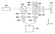
第1実施形態の計測装置の構成について説明する。図1に第1実施形態の計測装置の全体図を示す。この計測装置は、被計測物111の面位置を計測する。そして、面全体で各位置の計測を行うことにより、被計測物111の面の形状を求めることができる。被計測物111の表面は粗面であることを想定している。第1実施形態の計測装置は、ヘテロダイン方式を用いて干渉信号の位相を算出する。光源101はヘテロダイン光源であり、周波数fSのS偏光と、周波数fPのP偏光の光とを射出する。これらの光は、無偏光ビームスプリッタ102に入射し、入射した光の一部が無偏光ビームスプリッタ102で反射し、残部が無偏光ビームスプリッタ102を透過する。
[First Embodiment]
Configuration of Measuring Device The configuration of the measuring device according to the first embodiment will be described. FIG. 1 shows an overall view of the measuring apparatus according to the first embodiment. This measuring apparatus measures the surface position of the
無偏光ビームスプリッタ102で反射した光は、偏光軸が斜め45度に配置された検光子103を透過する。検光子103を透過した光は集光レンズ104に入射し、検出器105で受光される。検出器105で受光される干渉信号を基準信号と称する。一方、無偏光ビームスプリッタ102を透過した光は、偏光ビームスプリッタ106に入射し、S偏光の光は偏光ビームスプリッタ106で反射し、P偏光の光は偏光ビームスプリッタ106を透過する。偏光ビームスプリッタ106で反射したS偏光の光はλ/4波長板107を透過し円偏光になり、参照ミラー108の参照面で反射され、λ/4波長板107を再び透過してP偏光になり、偏光ビームスプリッタ106に再び入射する。偏光ビームスプリッタ106に再び入射した光は、P偏光なので偏光ビームスプリッタ106を透過する。この参照面で反射された光を参照光と称する。
The light reflected by the
一方、最初に偏光ビームスプリッタ106を透過したP偏光の光は、λ/4波長板109を透過し円偏光になり、集光レンズ110でビーム径が絞られ、ビームのスポット位置近傍に配置された被計測物111の表面で反射される。反射されてビーム径が広がった光は、集光レンズ110で平行光になり、λ/4波長板109を再び透過してS偏光になり、偏光ビームスプリッタ106に再び入射する。偏光ビームスプリッタ106に再び入射した光は、S偏光なので偏光ビームスプリッタ106で反射される。この被計測物111の表面で反射された光を計測光と称する。参照光及び計測光は、偏光ビームスプリッタ106で合波されて干渉光を生成する。干渉光は、偏光軸が斜め45度に配置された検光子112を透過する。検光子112を透過した干渉光は集光レンズ113に入射し、検出器114で受光される。検出器114で受光される干渉光の干渉信号を計測信号と称する。
On the other hand, the P-polarized light that first passes through the polarizing
検出器105及び検出器114で受光された信号は処理部115に送られる。処理部115は、受信した信号を処理して、被計測物111の表面上の計測光が照射された点の面位置に対応する位相を算出する。処理部115は、被計測物111をXY方向に移動させながら、各点の位相を算出することで、被計測物111の面形状を求める。被計測物111の表面は、粗面であるため凹凸を持っており、XY方向に移動させた場合、その凹凸によって面位置(Z方向の位置)が変化し、ドップラーシフトが発生する。
Signals received by the
干渉信号と面位置(Z方向の位置)との関係
被計測物111上のビームが照射されている点(x,y)の位相を、ドップラーシフト分を含めてφ(x,y,t)とする。すなわち、位相φ(x,y,t)は、計測光と参照光との光路長差に対応する。そのとき、ある時刻tでの基準信号Iref(t)と計測信号Isig(t,φ(x,y,t))とは、それぞれ式1、式2で表わされる。
Iref(t)=C0 ref+C1 refcos(2πΔft)・・・(1)
Isig(t,φ(x,y,t))=C0 sig(x,y,t)+C1 sig(x,y,t)cos(2πΔft−φ(x,y,t))・・・(2)
一般的にビート周波数と呼ばれるΔfは、式3で表わされる。
Δf=fs−fp・・・(3)
このビート周波数Δfは、例えば、AOM(音響光学素子)やゼーマン効果を用いて生成される。AOMは、結晶中を伝搬している超音波が疑似的な回折格子の役割をすることによって、入射光の周波数を超音波の周波数分だけ変調した回折光を発生させる光学素子である。ゼーマン効果は、レーザ内に磁場を印加することにより、原子の発光スペクトルが僅かに分離する効果のことをいう。式1及び式2において、C0 ref、C1 ref、C0 sig(x,y,t)、C1 sig(x,y,t)は、比例係数である。計測信号Isigの比例係数C0 sig(x,y,t)、C1 sig(x,y,t)は、(x,y,t)の関数となっている。その理由は、被計測物111において計測光が照射される点(x,y)の位置が時刻tとともに変化し、それによって被計測物111の表面における反射率が変化するためである。
Relationship between interference signal and surface position (position in Z direction ) The phase of point (x, y) irradiated with beam on
I ref (t) = C 0 ref + C 1 ref cos (2πΔft) (1)
I sig (t, φ (x, y, t)) = C 0 sig (x, y, t) + C 1 sig (x, y, t) cos (2πΔft−φ (x, y, t)) (2)
Δf generally called a beat frequency is expressed by Equation 3.
Δf = f s -f p ··· ( 3)
The beat frequency Δf is generated using, for example, AOM (acousto-optic element) or Zeeman effect. The AOM is an optical element that generates diffracted light in which the frequency of incident light is modulated by the frequency of the ultrasonic wave by the ultrasonic wave propagating in the crystal serving as a pseudo diffraction grating. The Zeeman effect refers to an effect in which the emission spectrum of atoms is slightly separated by applying a magnetic field in the laser. In
ドップラーシフトfDopは、式4で表わされる。ここで、v(x,y,t)は面位置zの変化速度であり、λsigは計測光路側の光源波長である。
fDop=dφ(x,y,t)/dt=2v(x,y,t)/λsig・・・(4)
したがって、求めるべき面位置z(x,y,t)は、式5で表わされる。
z(x,y,t)=∫v(x,y,t)dt・・・(5)
したがって、処理部115は、式1の基準信号Irefと式2の計測信号IsigとからドップラーシフトfDopを含む位相φ(x,y,t)を算出し、そこから面位置zの変化速度v(x,y,t)を算出し、最後にその速度を積分することで面位置zを求める。
The Doppler shift f Dop is expressed by Equation 4. Here, v (x, y, t) is a change speed of the surface position z, and λ sig is a light source wavelength on the measurement optical path side.
f Dop = dφ (x, y, t) / dt = 2v (x, y, t) / λ sig (4)
Accordingly, the surface position z (x, y, t) to be obtained is expressed by
z (x, y, t) = ∫v (x, y, t) dt (5)
Therefore, the
面位置zの算出
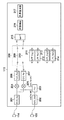
図2を用いて第1実施形態の位相算出回路を説明する。第1実施形態の特徴となるローパスフィルタ切り換え回路部分について、次数の接続と次数の接続誤差の説明も加えて特に詳細に説明する。図2には、検出器105及び114と処理部115の詳細が示されている。
Calculation of Surface Position z The phase calculation circuit of the first embodiment will be described with reference to FIG. The low-pass filter switching circuit portion, which is a feature of the first embodiment, will be described in detail in particular with the description of the order connection and the order connection error. FIG. 2 shows details of the
式1で表わされる基準信号Irefは検出器105で、式2で表わされる計測信号Isigは検出器114で受信され、処理部115に送られる。基準信号Iref及び計測信号Isigは、アナログデジタル変換器(ADC)201,202によりデジタル信号に変換される。例えば、ビート周波数Δfが20MHzである場合、ADCのサンプリング周波数は100MHz程度必要となる。
The reference signal I ref represented by
次に、フェイズロックループ(PIL)203は、デジタル化された基準信号Irefを基にsin(2πΔft)及びcos(2πΔft)の2つの信号を生成する。混合器204は、デジタル化された計測信号Isigと、PIL203によって生成されたsin(2πΔft)との積算信号を生成する。混合器205は、デジタル化された計測信号Isigと、PIL203によって生成されたcos(2πΔft)との積算信号を生成する。混合器204で生成されたデジタル信号は、式6で表わされる。一方、混合器205で生成されたデジタル信号は、式7で表わされる。
(1/2)C1 sig(x,y,t)sin(φ(x,y,t))+C0 sig(x,y,t)sin(2πΔft)+(1/2)C1 sig(x,y,t)sin(4πΔft−φ(x,y,t))・・・(6)
(1/2)C1 sig(x,y,t)cos(φ(x,y,t))+C0 sig(x,y,t)cos(2πΔft)+(1/2)C1 sig(x,y,t)cos(4πΔft−φ(x,y,t))・・・(7)
混合器204,205で生成されたデジタル信号は、それぞれ、第1項が周波数φ(x,y,t)成分、第2項が周波数Δf成分、第3項が周波数(2Δf−φ(x,y,t))成分である。したがって、位相φ(x,y,t)を算出するためには、まず第2項成分と第3項成分とを除去する必要がある。カスケード積算コム(CIC)フィルタ206,207は、それぞれ、混合器204,205で生成されたデジタル信号から第2項、第3項成分を除去する。周波数fに対してCICフィルタの周波数特性H(f)は、式8で与えられる。ここで、fsamplingは、ADCのサンプリング周波数、R、M、Nは、フィルタの形状を決定するCICフィルタ206,207固有のパラメータである。
Next, the phase lock loop (PIL) 203 generates two signals of sin (2πΔft) and cos (2πΔft) based on the digitized reference signal I ref . The
(1/2) C 1 sig (x, y, t) sin (φ (x, y, t)) + C 0 sig (x, y, t) sin (2πΔft) + (1/2) C 1 sig ( x, y, t) sin (4πΔft−φ (x, y, t)) (6)
(1/2) C 1 sig (x, y, t) cos (φ (x, y, t)) + C 0 sig (x, y, t) cos (2πΔft) + (1/2) C 1 sig ( x, y, t) cos (4πΔft−φ (x, y, t)) (7)
In the digital signals generated by the

図3にfsampling=100MHz、R=5、M=2、N=3の場合のCICフィルタ206,207の周波数特性H(f)を示す。図3において、縦軸はゲイン[dB]、横軸は周波数[Hz]である。また、図3には、ビート周波数Δf=20MHz、ドップラーシフトfDop=2MHzの場合における式6と式7の第1〜3項までの周波数成分を矢印で示してある。CICフィルタ206,207は、式6と式7における第1項成分に対して、第2項成分、第3項成分を十分に低減する。したがって、CICフィルタ206,207を透過したデジタル信号はそれぞれ式9、式10で表わされる。ここで、GCICはCICフィルタ206,207のゲインを示す。式9で表わされる信号は、計測光と参照光との光路長差に対応する位相φを有するサイン信号である。式10で表わされる信号は、計測光と参照光との光路長差に対応する位相φを有するコサイン信号である。
(GCIC/2)C1 sig(x,y,t)sin(φ(x,y,t))・・・(9)
(GCIC/2)C1 sig(x,y,t)cos(φ(x,y,t))・・・(10)
次に、図2において点線で囲まれた、ローパスフィルタ(LPF)切り換え回路208について詳細に説明する。LPF切り換え回路208は、第1実施形態における特徴部分である。検出器114により検出された計測信号が高いS/N比の場合、CICフィルタ206,207を透過したデジタル信号は、式9及び式10のようになる。このような場合、LPF切り換え回路208は、図2に示すように、デジタル信号がアークタンジェント計算器215まで直通するように直通回路209,210を用いる。
FIG. 3 shows the frequency characteristics H (f) of the CIC filters 206 and 207 when f sampling = 100 MHz, R = 5, M = 2, and N = 3. In FIG. 3, the vertical axis represents gain [dB], and the horizontal axis represents frequency [Hz]. Also, in FIG. 3, the frequency components of the first to third terms of Expression 6 and Expression 7 when the beat frequency Δf = 20 MHz and the Doppler shift f Dop = 2 MHz are indicated by arrows. The CIC filters 206 and 207 sufficiently reduce the second term component and the third term component with respect to the first term component in Equations 6 and 7. Therefore, the digital signals that have passed through the CIC filters 206 and 207 are expressed by Expression 9 and
(G CIC / 2) C 1 sig (x, y, t) sin (φ (x, y, t)) (9)
(G CIC / 2) C 1 sig (x, y, t) cos (φ (x, y, t)) (10)
Next, the low-pass filter (LPF) switching
アークタンジェント計算器215は、式9、式10で示される2つのデジタル信号を用いて式11で示されるアークタンジェントを計算する。
tan−1[{(GCIC/2)C1 sig(x,y,t)sin(φ(x,y,t))}/{(GCIC/2)C1 sig(x,y,t)cos(φ(x,y,t))}]=φ(x,y,t)・・・(11)
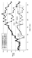
次数接続計算器216は、式11の計算結果を用いて次数を接続する。ここで、次数接続と次数接続誤差について図4及び図5を用いて説明する。まず、計測信号が高いS/N比である場合について図4を用いて説明する。図4において、縦軸は位相[rad]、横軸はデータ番号である。アークタンジェント計算器215によって算出された位相φ(x,y,t)を、図4内では三角点と点線で表わす。位相φ(x,y,t)は、式11によって−πから+πの範囲で計算される。次数接続計算器216は、あるデータとその次のデータとの位相差がπ以上あるものに対して、次数Nを接続する。例えば、あるデータに対してその次のデータが−π以上変化すれば、次数Nを(N+1)とし、+π以上変化すれば、次数Nを(N−1)とする。そして、次数接続後のデータをN+φとして表わす。次数接続後のデータを図4内では四角点と実線で表わす。また、図4内の矢印は、次数接続を実施したデータ点と次数接続の際の計算を示す。図4に示すように、次数接続が成功していれば、滑らかな位相変化が得られる。
The
tan -1 [{(G CIC / 2) C 1 sig (x, y, t) sin (φ (x, y, t))} / {(G CIC / 2) C 1 sig (x, y, t ) Cos (φ (x, y, t))}] = φ (x, y, t) (11)
The
計測信号が低いS/N比である場合について図5を用いて説明する。ここで、位相の変化は図4の場合と同じであるとする。計測信号が低いS/N比である場合、CICフィルタ206,207を透過したデジタル信号は、高周波のノイズ成分が付加され、式12、式13のようになる。Noiseは、ノイズ成分である。ノイズ成分は、光源101の周波数の揺らぎ、電気回路系の誤差、光学素子の製作誤差及び調整誤差、被計測物111の表面形状等に由来する。ノイズ成分の最も大きな要因は、被計測物111の表面形状に由来するものである。
(GCIC/2)C1 sig(x,y,t)sin(φ(x,y,t))+Noise・・・(12)
(GCIC/2)C1 sig(x,y,t)cos(φ(x,y,t))+Noise・・・(13)
このノイズ成分によって、アークタンジェント計算器215により算出される位相φ(x,y,t)は大きなばらつきを持つ。このばらつきの様子を図5内では三角点と点線(太線)で表わす。計測信号が高いS/N比である場合を細い点線で示す。この位相φ(x,y,t)を用いて次数接続計算器216は次数を接続する。仮に次数接続が正しく行えた場合を図5内では四角点と太い実線で表わす。また、計測信号が高いS/N比である場合を細い実線で示す。しかし、次数接続計算器216は、実際には次数接続を間違え、図5のデータ番号18のように、N=N−1の計算を実施してしまう。なお、図4においてはデータ番号18においてそのような計算はしない。図5内ではその誤った次数接続の計算を斜体かつ下線付きの数式として強調してある。このように次数接続を誤った場合を、図5内では丸点と一点鎖線で表わす。従って、データ番号18以降、全てのデータの値が2πだけずれることとなる。以上が次数接続と次数接続誤差の説明となる。
A case where the measurement signal has a low S / N ratio will be described with reference to FIG. Here, the phase change is the same as in FIG. When the measurement signal has a low S / N ratio, the digital signal that has passed through the CIC filters 206 and 207 is added with a high-frequency noise component, as shown in Equations 12 and 13. Noise is a noise component. The noise component is derived from the fluctuation of the frequency of the
(G CIC / 2) C 1 sig (x, y, t) sin (φ (x, y, t)) + Noise (12)
(G CIC / 2) C 1 sig (x, y, t) cos (φ (x, y, t)) + Noise (13)
Due to this noise component, the phase φ (x, y, t) calculated by the
第1実施形態の特徴部分であるLPF切り換え回路208の説明の続きに戻る。図5で説明したように、計測信号が低いS/N比で、次数の接続誤差が発生するような場合には、CICフィルタ206,207とアークタンジェント計算器215との間にLPFを接続させる。LPF211,212は、サイン信号、コサイン信号に含まれるノイズ成分を低減するようにサイン信号、コサイン信号を補正する補正処理部を構成する。図6は、このような場合の位相算出回路を示す。LPF211,212は、周波数fに対して式14で表わされる周波数特性H(f)を持つ。ここで、fcutoffはカットオフ周波数である。
H(f)=1/{1+(f/fcutoff)2}1/2・・・(14)
図7にfcutoff=100kHzの場合のLPF211,212の周波数特性H(f)を示す。図7において、縦軸はゲイン[dB]、横軸は周波数[Hz]であるが、図3とは異なり、横軸が対数表示になっている。式12、式13で示されるデジタル信号にLPFを透過させることにより、式12及び式13のノイズ成分を低減することが可能となる。したがって、図5で説明したような次数の接続誤差を低減することが可能となる。デジタル信号にLPFを透過させることは、計測速度をカットオフ周波数で制限することとなる。LPFを用いない場合(図2の場合)で、λsigが1μm、計測可能なドップラーシフトが2MHzであれば、計測可能な最大速度は1m/secである。しかし、LPFを用いた場合(図6の場合)にfcutoff=100kHzであれば、計測可能な最大速度は50nm/secとなる。
Returning to the continuation of the description of the
H (f) = 1 / {1+ (f / f cutoff ) 2 } 1/2 (14)
FIG. 7 shows the frequency characteristics H (f) of the
そこで第1実施形態では、式12及び式13で示されるデジタル信号のノイズの大きさによって、つまり、S/N比によって、LPFのカットオフ周波数fcutoffを切り換える。これは図6内でのLPF213及び214を用いることに相当する。例えば、LPF213,214のカットオフ周波数をfcutoff=1000kHzに設定しておけば、ノイズ成分の低減率はLPF211,212より低下するが、計測可能な最大速度は500mm/secに増大する。このように、LPFを用いない、あるいはLPFを用いる場合でも適宜カットオフ周波数fcutoffが異なるLPFに切り換えることで、計測可能な最大速度を必要以上に落とすことなく、次数の接続誤差を低減することが可能となる。
Therefore, in the first embodiment, the cutoff frequency f cutoff of the LPF is switched according to the noise level of the digital signal expressed by Expression 12 and Expression 13, that is, the S / N ratio. This corresponds to using the
LPFの切り換え動作の判定について図8を用いて説明する。図8は、被計測物111の表面における入射光と反射光との状態を示す。図8中、計測位置Aに入射する光とその反射光を実線の矢印で、計測位置Bに入射する光とその反射光を点線の矢印で示す。計測位置Aにおいては、被計測物111の表面への入射角度はゼロ度近傍である為、検出器114へ戻る反射光の光量は大きい。したがって、計測位置Aの近傍において干渉信号の強度のばらつきは少なく、干渉信号のS/N比は高い。一方、計測位置Bにおいては、被計測物111の表面への入射角度はある程度の角度を持つ。そのため、主な反射光は検出器114の方向とは異なる方向へ行き、検出器114へ戻る反射光の光量は小さくなる。したがって、干渉信号は、ノイズの影響を受けやすくなり、強度のばらつきは大きく、その結果、計測位置Bにおける干渉信号のS/N比は低下する。つまり、計測光が入射角度を持たない場合はS/N比が増加し、入射角度を持つ場合はS/N比が低下する。計測光がどのような入射角度を持つかの情報は、被計測物111の面形状の設計値から得ることも可能である。したがって、LPFの切り換えを実施するか否かは、処理部115が、被計測物111の設計値などに基づいて判定する。具体的には、まず設計値のデータから被計測物111の表面への入射角がどの程度になるかを計算しておく。例えば、入射角が5度未満であればLPFを用いず、入射角が5〜10度であればカットオフ周波数が1000kHzのLPFを用い、入射角が10度以上であればカットオフ周波数が100kHzのLPFを用いる、といったように設定する。
The determination of the LPF switching operation will be described with reference to FIG. FIG. 8 shows a state of incident light and reflected light on the surface of the
LPF切り換え回路208は、S/N比を常にモニタリングしておき、そのモニタリング結果に基づいてLPFの切り換えを判断するようにしてもよい。すなわち、検出器114から出力された干渉信号の強度のばらつきや当該干渉信号から得られた信号の強度のばらつきに基づいてLPFの切り換えを判断することができる。例えば、LPF切り換え回路208は、アークタンジェント計算器215により算出される、干渉信号から得られた位相信号の強度のバラツキを常にモニタリングする。そして、そのバラツキがある閾値(例えばπ/3)を超えた場合、LPF切り換え回路208は、カットオフ周波数がより小さいLPFに切り換える。また、LPF切り換え回路208は、干渉信号のS/Nを直接計測した結果に基づいてLPFの切り換えを判断しても良い。
The
最後に、測長演算器217は、次数接続された位相{N+φ(x,y,t)}を式4及び式5を用いて面位置zに換算する。以上のように第1実施形態の計測装置は、干渉信号のS/N比が低い場合においても、次数の接続誤差を低減することができる。
Finally, the
〔第2実施形態〕
第2実施形態の計測装置は、第1実施形態の計測装置の変形であり、第1実施形態の計測装置と2つの点で相違する。第1の相違点は、複数の波長を用いた合成波長で被計測物111の面位置を計測すること、第2の相違点は、LPFを切り換える機能を有せず1つのLPFを常に用いることである。
[Second Embodiment]
The measurement device of the second embodiment is a modification of the measurement device of the first embodiment, and differs from the measurement device of the first embodiment in two respects. The first difference is that the surface position of the object to be measured 111 is measured with a synthetic wavelength using a plurality of wavelengths, and the second difference is that one LPF is always used without the function of switching the LPF. It is.
計測装置の構成
図9は第2実施形態の計測装置を示す。第2光源116は第1光源101の第1光の第1波長とは僅かに異なる第2波長の第2光を生成する。光源101の波長をλ1、光源116の波長をλ2とする。λ1、λ2ともヘテロダイン光源である為、それぞれP偏光及びS偏光で、ビート周波数分、周波数が異なる。ここで、λ1、λ2は、例えば約1μmで、λ1、λ2の差は10nmであり、周波数換算で3THz異なるが、各光源101,116のP偏光とS偏光の差であるビート周波数は第1実施形態でも述べたように20MHz程度である。
Configuration of Measuring Device FIG. 9 shows a measuring device according to the second embodiment. The second
これらの光は、分光フィルタ117によって合波される。分光フィルタ117は、光源101のλ1の光が透過し、光源116のλ2の光が反射するような誘電体多層膜がコーティングしてある。この分光フィルタ117は、ビート周波数程度の差では分光特性に差はない。合波された光は無偏光ビームスプリッタ102に入射し、入射光の一部が無偏光ビームスプリッタ102で反射し、残部が無偏光ビームスプリッタ102を透過する。無偏光ビームスプリッタ102で反射された光は検光子103を透過し、分光フィルタ118に入射する。分光フィルタ118は、分光フィルタ117と同じもので、光源116の光は分光フィルタ118で反射し、光源101の光は分光フィルタ118を透過する。分光フィルタ118を透過した光源101の光は、集光レンズ104に入射し、検出器105により受光される。分光フィルタ118で反射した光源116の光は、集光レンズ119に入射し、検出器120により受光される。これら2波長の基準信号は、処理部115に送られる。
These lights are combined by the
一方、無偏光ビームスプリッタ102を透過した光は、偏光ビームスプリッタ106に入射する。このあとの工程は、検光子112を透過するまで、第1実施形態と同じであるので、説明を省略する。検光子112を透過した光は、分光フィルタ121に入射する。分光フィルタ121は、分光フィルタ117と同じもので、光源116の光は分光フィルタ121で反射し、光源101の光は分光フィルタ121を透過する。分光フィルタ121を透過した光源101の光を用いて生成された第1干渉光は、集光レンズ113に入射し、第1検出器114により受光される。分光フィルタ121を反射した光源116の光を用いて生成された第2干渉光は、集光レンズ122に入射し、第2検出器123により受光される。第1検出器114が出力する第1干渉信号と第2検出器123が出力する第2干渉信号とは、処理部115に送られる。
On the other hand, the light transmitted through the
面位置の算出
次に合成波長Λを用いた面位置の算出について説明する。λ1、λ2を用いて、その合成波長Λは式15で表わされる。
Λ=λ1λ2/|λ1−λ2|・・・(15)
また、合成波長Λに対応する干渉信号の位相は式16で表わされる。ここで、φ1(x,y,t)はλ1による位相、φ2(x,y,t)はλ2による位相である。
{φ1(x,y,t)−φ2(x,y,t)}・・・(16)
したがって、{φ1(x,y,t)−φ2(x,y,t)}を高精度に算出することにより、合成波長Λによる計測が可能となる。第2実施形態では、合成波長Λは光源波長λ1とλ2に対して波長が大きい。したがって、ドップラーシフトの発生量は光源101,116の波長λ1、λ2を用いた場合よりも低減する。例えば、波長1μmと1.01μmの合成波長は101μmであり、ドップラーシフトの発生量は波長1μmの場合よりも約1/100に低減する。さらに合成波長Λを用いることで被計測物111に照射されているスポット径内の粗さが波長λ1、λ2よりも大きい場合も計測が可能となる。一方、計測の目盛りとしても合成波長Λの方が大きくなる為、計測精度は低下する。ただし、実際の被計測物111の必要計測精度は高々1μm程度であり、合成波長101μmに対して1/100程度の位相計測精度は利用可能である為、合成波長Λの計測精度で十分である。
Calculation of Surface Position Next, calculation of the surface position using the combined wavelength Λ will be described. Using λ 1 and λ 2 , the combined wavelength Λ is expressed by
Λ = λ 1 λ 2 / | λ 1 −λ 2 | (15)
Further, the phase of the interference signal corresponding to the combined wavelength Λ is expressed by Expression 16. Here, φ 1 (x, y, t) is a phase due to λ 1 , and φ 2 (x, y, t) is a phase due to λ 2 .
{Φ 1 (x, y, t) −φ 2 (x, y, t)} (16)
Therefore, by calculating {φ 1 (x, y, t) −φ 2 (x, y, t)} with high accuracy, measurement using the combined wavelength Λ becomes possible. In the second embodiment, the combined wavelength Λ is larger than the light source wavelengths λ 1 and λ 2 . Therefore, the amount of Doppler shift generated is reduced as compared with the case where the wavelengths λ 1 and λ 2 of the
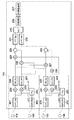
図10に第2実施形態の位相算出回路を示す。図10内の点線と一点鎖線で囲まれた領域は、検出器114,105,123,120、ADC201,202,218,219、PIL203,220、混合器204,205,221,222、CICフィルタ206,207,223,224である。点線で囲まれた領域は、光源101の波長λ1に対する処理部分であり、一点鎖線で囲まれた領域は、光源116の波長λ2に対する処理部分である。点線内、一点鎖線内の各部の処理内容は第1実施形態と同じであると為、説明を省略する。
FIG. 10 shows a phase calculation circuit according to the second embodiment. The regions surrounded by the dotted line and the alternate long and short dash line in FIG. , 207, 223, and 224. A region surrounded by a dotted line is a processing portion for the wavelength λ 1 of the
CICフィルタ206,207,223,224を透過するデジタル信号は、それぞれ式17〜式20で表わされる。ここで、説明を簡略化する為、比例係数を省いた。
sin(φ1(x,y,t))・・・(17)
cos(φ1(x,y,t))・・・(18)
sin(φ2(x,y,t))・・・(19)
cos(φ2(x,y,t))・・・(20)
式17〜式20で示されるデジタル信号は混合器225〜228によって積算される。混合器225〜228を透過したデジタル信号は、それぞれ式21〜式24で表わされる。
sin(φ1(x,y,t))cos(φ2(x,y,t))・・・(21)
cos(φ1(x,y,t))sin(φ2(x,y,t))・・・(22)
sin(φ1(x,y,t))sin(φ2(x,y,t))・・・(23)
cos(φ1(x,y,t))cos(φ2(x,y,t))・・・(24)
式21〜式24で示されるデジタル信号は、減算器229と加算器230によってそれぞれ式25と式26で表わされるものとなる。
sin(φ1(x,y,t))cos(φ2(x,y,t))−cos(φ1(x,y,t))sin(φ2(x,y,t))=sin(φ1(x,y,t)−φ2(x,y,t))・・・(25)
sin(φ1(x,y,t))sin(φ2(x,y,t))+cos(φ1(x,y,t))cos(φ2(x,y,t))=cos(φ1(x,y,t)−φ2(x,y,t))・・・(26)
第1実施形態で述べたように、低いS/N比である場合は高周波のノイズ成分が付加される為に、減算器229と加算器230を通過したデジタル信号は式27、式28で表わされるものとなる。
sin(φ1(x,y,t)−φ2(x,y,t))+Noise・・・(27)
cos(φ1(x,y,t)−φ2(x,y,t))+Noise・・・(28)
式27、式28で示されるデジタル信号はLPF231,232を通過する。LPF231,232は、高周波ノイズ成分を低減する。上述したように、第2実施形態では合成波長を用いている為、ドップラーシフト発生量が低減されている。例えば、合成波長を用いずに、単一光源波長1μm、LPFのカットオフ周波数fcutoff=100kHzで計測する場合、計測可能な最大速度は50mm/secで制限される。しかし、第2実施形態では、光源波長1μmと1.01μmの合成波長101μmを用いることにより、計測可能な最大速度は5m/secまで増大する。したがって、第1実施形態に比べて計測可能な最大速度には十分な余裕があり、LPFを切り換える必要性が小さい。そこで、第2実施形態では、LPFを切り換える機構を持たずに、低いS/N比の場合に発生する高周波ノイズ成分を除去することが可能となる。
The digital signals that pass through the CIC filters 206, 207, 223, and 224 are expressed by Expressions 17 to 20, respectively. Here, in order to simplify the explanation, the proportionality coefficient is omitted.
sin (φ 1 (x, y, t)) (17)
cos (φ 1 (x, y, t)) (18)
sin (φ 2 (x, y, t)) (19)
cos (φ 2 (x, y, t)) (20)
The digital signals represented by the equations 17 to 20 are integrated by the
sin (φ 1 (x, y, t)) cos (φ 2 (x, y, t)) (21)
cos (φ 1 (x, y, t)) sin (φ 2 (x, y, t)) (22)
sin (φ 1 (x, y, t)) sin (φ 2 (x, y, t)) (23)
cos (φ 1 (x, y, t)) cos (φ 2 (x, y, t)) (24)
The digital signals represented by
sin (φ 1 (x, y , t)) cos (φ 2 (x, y, t)) - cos (φ 1 (x, y, t)) sin (φ 2 (x, y, t)) = sin (φ 1 (x, y, t) −φ 2 (x, y, t)) (25)
sin (φ 1 (x, y, t)) sin (φ 2 (x, y, t)) + cos (φ 1 (x, y, t)) cos (φ 2 (x, y, t)) = cos (Φ 1 (x, y, t) −φ 2 (x, y, t)) (26)
As described in the first embodiment, when the S / N ratio is low, a high-frequency noise component is added. Therefore, the digital signals that have passed through the
sin (φ 1 (x, y, t) −φ 2 (x, y, t)) + Noise (27)
cos (φ 1 (x, y, t) −φ 2 (x, y, t)) + Noise (28)
The digital signals represented by
アークタンジェント計算器215は、LPF231,232を透過したデジタル信号から式29で示される位相データを得る。
{φ1(x,y,t)−φ2(x,y,t)}・・・(29)
算出された位相データは、その後、次数接続計算器216及び測長演算器217を通過し、面位置zに換算される。以上のように第2実施形態によって、干渉信号のS/N比が低い場合においても、次数接続誤差を低減することができる。第1、第2実施形態ではヘテロダイン方式を用いた。しかし、ホモダイン方式においても、算出する位相のサイン成分とコサイン成分を算出した後にアークタンジェント演算を施すことで共通するから、本発明はホモダイン方式にも応用可能である。
The
{Φ 1 (x, y, t) −φ 2 (x, y, t)} (29)
Thereafter, the calculated phase data passes through the
〔第3実施形態〕
第3実施形態の計測装置と第1実施形態の計測装置との差異は、干渉信号の位相のサイン成分及びコサイン成分のノイズ成分を除去するのではなく、バンドパスフィルタ(BPF)を用いてビート周波数の干渉信号の高周波ノイズ成分を除去することである。第3実施形態の計測装置は、処理部115の内部のみ、第1実施形態の計測装置と異なる。
[Third Embodiment]
The difference between the measurement apparatus of the third embodiment and the measurement apparatus of the first embodiment is that the noise component of the phase of the interference signal is not removed but the noise component is beaten using a bandpass filter (BPF). This is to remove the high frequency noise component of the frequency interference signal. The measurement device of the third embodiment is different from the measurement device of the first embodiment only in the
次に、第3実施形態における面位置の算出手法について説明をする。図11に第3実施形態の位相算出回路を示す。第1実施形態と異なる点は、ADC201を出力した計測信号のデジタル信号が、点線で囲まれたBPF切り換え回路233を通過することである。BPF切り換え回路233は、直通回路234とBPF235とを含む。BPF235は、中心周波数がビート周波数Δfと同じようになるように設計されている。したがって、BPF235は、ビート周波数以外のノイズ成分を除去可能である。また第1実施形態と同じように、干渉信号が高いS/N比の場合と低いS/N比の場合とで、直通回路234とBPF235との回路を切り換えることができる。切り換えの判断は、第1実施形態と同様である。したがって、干渉信号のS/N比が低い場合においても、高いS/N比の場合と同等の信号が得られ、その結果、次数接続計算器216は、次数の接続誤差を低減できる。また、図11においてBPF235として1種類のみを記載したが、バンド幅が異なる複数のBPFを準備しておき、発生するドップラーシフト量などに応じて使用するBPFを切り換えてもよい。
Next, a method for calculating the surface position in the third embodiment will be described. FIG. 11 shows a phase calculation circuit according to the third embodiment. The difference from the first embodiment is that the digital signal of the measurement signal output from the
第3実施形態ではヘテロダイン方式とBPFを用いた位相算出法で説明した。しかし、ホモダイン方式においてはBPFの代わりにLPFを用いれば同等の効果が得られる為、本発明はホモダイン方式にも応用可能である。 In the third embodiment, the heterodyne method and the phase calculation method using BPF have been described. However, in the homodyne system, the same effect can be obtained if LPF is used instead of BPF, and therefore the present invention can also be applied to the homodyne system.
Claims (9)
前記干渉光を検出して干渉信号を出力する検出器と、
前記検出器から出力された干渉信号から得られる、前記計測光と前記参照光との光路長差に対応する位相を有するサイン信号及びコサイン信号に基づいて前記面位置を求める処理部と、
を備え、
前記処理部は、前記サイン信号及びコサイン信号に含まれるノイズ成分を低減するように前記サイン信号及びコサイン信号を補正する補正処理部を含む、
ことを特徴とする計測装置。 A measuring device that detects interference light between the measurement light reflected by the measurement object and the reference light reflected by the reference surface, and measures the surface position of the measurement object,
A detector that detects the interference light and outputs an interference signal;
A processing unit for obtaining the surface position based on a sine signal and a cosine signal having a phase corresponding to an optical path length difference between the measurement light and the reference light, obtained from an interference signal output from the detector;
With
The processing unit includes a correction processing unit that corrects the sine signal and the cosine signal so as to reduce a noise component included in the sine signal and the cosine signal.
A measuring device characterized by that.
前記補正を行うと判定された場合に、前記補正処理部は、前記サイン信号及びコサイン信号を補正し、前記処理部は、補正されたサイン信号及びコサイン信号に基づいて前記面位置を求め、
前記補正を行わないと判定された場合に、前記処理部は、補正されなかったサイン信号及びコサイン信号に基づいて前記面位置を求める、
ことを特徴とする請求項1に記載の計測装置。 The processing unit is based on at least one of a design value of a surface shape of the measurement object, a variation in intensity of an interference signal output from the detector, and a variation in intensity of a signal obtained from the interference signal. To determine whether to perform correction by the correction processing unit,
When it is determined to perform the correction, the correction processing unit corrects the sine signal and the cosine signal, and the processing unit obtains the surface position based on the corrected sine signal and cosine signal,
When it is determined not to perform the correction, the processing unit obtains the surface position based on a sine signal and a cosine signal that have not been corrected,
The measuring apparatus according to claim 1.
前記干渉光を検出して干渉信号を出力する検出器と、
前記検出器から出力された干渉信号から得られる、前記計測光と前記参照光との光路長差に対応する位相を有するサイン信号及びコサイン信号に基づいて前記面位置を求める処理部と、
を備え、
前記処理部は、前記干渉信号に含まれるノイズ成分を低減するように前記干渉信号を補正する補正処理部を含む、
ことを特徴とする計測装置。 A measuring device that detects interference light between the measurement light reflected by the measurement object and the reference light reflected by the reference surface, and measures the surface position of the measurement object,
A detector that detects the interference light and outputs an interference signal;
A processing unit for obtaining the surface position based on a sine signal and a cosine signal having a phase corresponding to an optical path length difference between the measurement light and the reference light, obtained from an interference signal output from the detector;
With
The processing unit includes a correction processing unit that corrects the interference signal so as to reduce a noise component included in the interference signal.
A measuring device characterized by that.
前記補正を行うと判定された場合に、前記補正処理部は前記干渉信号を補正し、前記処理部は、補正された干渉信号から導き出されたサイン信号及びコサイン信号に基づいて前記面位置を求め、
前記補正を行わないと判定された場合に、前記処理部は、補正されなかった干渉信号から導き出されたサイン信号及びコサイン信号に基づいて前記面位置を求める、
ことを特徴とする請求項3に記載の計測装置。 The processing unit is at least one of a design value of the surface shape of the object to be measured, a variation in the intensity of the detected interference signal output from the instrument, and a variation in the intensity of the signal obtained from the interference signal. To determine whether to perform correction by the correction processing unit based on
When it is determined to perform the correction, the correction processing unit corrects the interference signal, and the processing unit obtains the surface position based on the sine signal and the cosine signal derived from the corrected interference signal. ,
When it is determined not to perform the correction, the processing unit obtains the surface position based on a sine signal and a cosine signal derived from an interference signal that has not been corrected,
The measuring device according to claim 3.
第1波長の第1光を生成する第1光源と、
第2波長の第2光を生成する第2光源と、
前記第1光を用いて生成された第1干渉光を検出して第1干渉信号を出力する第1検出器と、
前記第2光を用いて生成された第2干渉光を検出して第2干渉信号を出力する第2検出器と、
前記第1干渉信号及び前記第2干渉信号に基づいて前記面位置を求める処理部と、
を備え、
前記処理部は、前記第1干渉信号及び前記第2干渉信号から前記第1波長及び前記第2波長の合成波長に対応する干渉信号の位相を有するサイン信号及びコサイン信号を求め、求められたサイン信号及びコサイン信号に含まれるノイズ成分を低減するように前記サイン信号及びコサイン信号を補正し、補正されたサイン信号及びコサイン信号を用いて前記面位置を求め、
前記合成波長は、前記第1波長及び前記第2波長よりも長い、
ことを特徴とする計測装置。 A measuring device that detects interference light between the measurement light reflected by the measurement object and the reference light reflected by the reference surface, and measures the surface position of the measurement object,
A first light source for generating first light of a first wavelength;
A second light source that generates second light of a second wavelength;
A first detector for detecting a first interference light generated using the first light and outputting a first interference signal;
A second detector for detecting a second interference light generated using the second light and outputting a second interference signal;
A processing unit for determining the surface position based on the first interference signal and the second interference signal;
With
The processing unit obtains a sine signal and a cosine signal having a phase of an interference signal corresponding to a combined wavelength of the first wavelength and the second wavelength from the first interference signal and the second interference signal, and the obtained sine Correcting the sine signal and cosine signal so as to reduce a noise component included in the signal and the cosine signal, and determining the surface position using the corrected sine signal and cosine signal,
The synthetic wavelength is longer than the first wavelength and the second wavelength;
A measuring device characterized by that.
前記干渉光を検出して干渉信号を出力する工程と、
前記出力された干渉信号から得られる、前記計測光と前記参照光との光路長差に対応する位相を有するサイン信号及びコサイン信号を、前記サイン信号及びコサイン信号に含まれるノイズ成分を低減するように補正する工程と、
補正されたサイン信号及びコサイン信号に基づいて前記面位置を求める工程と、
を含むことを特徴とする計測方法。 A measurement method for detecting the interference light between the measurement light reflected by the measurement object and the reference light reflected by the reference surface and measuring the surface position of the measurement object,
Detecting the interference light and outputting an interference signal;
A sine signal and a cosine signal obtained from the output interference signal and having a phase corresponding to an optical path length difference between the measurement light and the reference light are reduced in a noise component included in the sine signal and the cosine signal. A process of correcting to
Obtaining the surface position based on the corrected sine and cosine signals;
A measurement method comprising:
前記干渉光を検出して干渉信号を出力する工程と、
前記出力された前記干渉信号に含まれるノイズ成分を低減するように前記干渉信号を補正する工程と、
前記補正された干渉信号から前記計測光と前記参照光との光路長差に対応する位相を有するサイン信号及びコサイン信号を求め、求められたサイン信号及びコサイン信号に基づいて前記面位置を求める工程と、
含むことを特徴とする計測方法。 A measurement method for detecting the interference light between the measurement light reflected by the measurement object and the reference light reflected by the reference surface and measuring the surface position of the measurement object,
Detecting the interference light and outputting an interference signal;
Correcting the interference signal to reduce a noise component included in the output interference signal;
A step of obtaining a sine signal and a cosine signal having a phase corresponding to an optical path length difference between the measurement light and the reference light from the corrected interference signal, and obtaining the surface position based on the obtained sine signal and cosine signal. When,
A measuring method characterized by including.
Priority Applications (3)
| Application Number | Priority Date | Filing Date | Title |
|---|---|---|---|
| JP2012085895A JP2013217670A (en) | 2012-04-04 | 2012-04-04 | Measuring device and measuring method |
| EP13158297.5A EP2648044A3 (en) | 2012-04-04 | 2013-03-08 | Measurement apparatus and measurement method |
| US13/804,006 US20130268225A1 (en) | 2012-04-04 | 2013-03-14 | Measurement apparatus and measurement method |
Applications Claiming Priority (1)
| Application Number | Priority Date | Filing Date | Title |
|---|---|---|---|
| JP2012085895A JP2013217670A (en) | 2012-04-04 | 2012-04-04 | Measuring device and measuring method |
Publications (2)
| Publication Number | Publication Date |
|---|---|
| JP2013217670A true JP2013217670A (en) | 2013-10-24 |
| JP2013217670A5 JP2013217670A5 (en) | 2015-05-21 |
Family
ID=47827075
Family Applications (1)
| Application Number | Title | Priority Date | Filing Date |
|---|---|---|---|
| JP2012085895A Withdrawn JP2013217670A (en) | 2012-04-04 | 2012-04-04 | Measuring device and measuring method |
Country Status (3)
| Country | Link |
|---|---|
| US (1) | US20130268225A1 (en) |
| EP (1) | EP2648044A3 (en) |
| JP (1) | JP2013217670A (en) |
Cited By (1)
| Publication number | Priority date | Publication date | Assignee | Title |
|---|---|---|---|---|
| JP7293078B2 (en) | 2019-10-08 | 2023-06-19 | 株式会社ミツトヨ | Analysis device, analysis method, interference measurement system, and program |
Families Citing this family (2)
| Publication number | Priority date | Publication date | Assignee | Title |
|---|---|---|---|---|
| JP2014109481A (en) * | 2012-11-30 | 2014-06-12 | Canon Inc | Measurement method and measurement device |
| WO2016154780A1 (en) * | 2015-03-27 | 2016-10-06 | 浙江理工大学 | Laser interference wavelength lever-type absolute distance measurement apparatus and method |
Family Cites Families (9)
| Publication number | Priority date | Publication date | Assignee | Title |
|---|---|---|---|---|
| US5828454A (en) * | 1996-07-29 | 1998-10-27 | Gust; Gary R. | Optical heterodyne interferometer for measurement of ocular displacement |
| US6147755A (en) * | 1999-04-01 | 2000-11-14 | Trw Inc. | Dynamic optical phase state detector |
| US7428685B2 (en) | 2002-07-08 | 2008-09-23 | Zygo Corporation | Cyclic error compensation in interferometry systems |
| WO2004029671A2 (en) * | 2002-09-26 | 2004-04-08 | Prime Photonics, Inc. | Active q-point stabilization for linear interferometric sensors |
| US7640140B2 (en) * | 2003-03-07 | 2009-12-29 | Sensys Medical, Inc. | Method of processing noninvasive spectra |
| CN101015124B (en) * | 2004-09-08 | 2011-04-20 | 富士通半导体股份有限公司 | PLL frequency synthesizer |
| JP4465451B2 (en) | 2004-12-15 | 2010-05-19 | 独立行政法人産業技術総合研究所 | Method and apparatus for reducing periodic error of optical interferometer |
| US7576868B2 (en) * | 2007-06-08 | 2009-08-18 | Zygo Corporation | Cyclic error compensation in interferometry systems |
| US7956630B1 (en) * | 2008-04-15 | 2011-06-07 | Veeco Instruments, Inc. | Real-time effective-wavelength error correction for HDVSI |
-
2012
- 2012-04-04 JP JP2012085895A patent/JP2013217670A/en not_active Withdrawn
-
2013
- 2013-03-08 EP EP13158297.5A patent/EP2648044A3/en not_active Withdrawn
- 2013-03-14 US US13/804,006 patent/US20130268225A1/en not_active Abandoned
Cited By (1)
| Publication number | Priority date | Publication date | Assignee | Title |
|---|---|---|---|---|
| JP7293078B2 (en) | 2019-10-08 | 2023-06-19 | 株式会社ミツトヨ | Analysis device, analysis method, interference measurement system, and program |
Also Published As
| Publication number | Publication date |
|---|---|
| US20130268225A1 (en) | 2013-10-10 |
| EP2648044A2 (en) | 2013-10-09 |
| EP2648044A3 (en) | 2015-06-17 |
Similar Documents
| Publication | Publication Date | Title |
|---|---|---|
| JP4995016B2 (en) | Absolute position measuring apparatus and measuring method | |
| JP2014109481A (en) | Measurement method and measurement device | |
| US20140307263A1 (en) | Measuring apparatus and article manufacturing method | |
| JP2010112768A (en) | Measurement apparatus | |
| JP2008533447A (en) | Heterodyne reflectometer for film thickness monitoring and method for implementing the same | |
| WO2009017291A1 (en) | Scanning micrometer using heterodyne interferometer | |
| JP2000205814A (en) | Heterodyne interferometer | |
| JPWO2018070442A1 (en) | Optical angle modulation measuring apparatus and measuring method | |
| JP2013217670A (en) | Measuring device and measuring method | |
| US8724114B2 (en) | Interferometer and distance calculation method therefor | |
| JP5888111B2 (en) | Etching monitor device | |
| JP6975237B2 (en) | Glow discharge spectrophotometer including methods and instruments for measuring etching depth by differential polarization interferometry and such measuring instruments. | |
| US20120212746A1 (en) | Interferometer and measurement method | |
| JP5188127B2 (en) | Absolute position measuring apparatus and measuring method | |
| US6295131B1 (en) | Interference detecting system for use in interferometer | |
| JP4678587B2 (en) | Optical property measuring device | |
| JP6302853B2 (en) | OCT equipment | |
| JP2006064451A (en) | Interferometer | |
| JP3108866B2 (en) | Laser vibration displacement measuring device | |
| JP2011102751A (en) | Method and apparatus for measuring plate thickness of birefringent substrate | |
| JP7123333B2 (en) | Displacement measuring device | |
| JP4835908B2 (en) | Optical property measuring device | |
| JP3937798B2 (en) | Interferometer and position measuring device | |
| JP2024022043A (en) | Optical devices and spectroscopy | |
| JP2024017359A (en) | Optical devices and spectroscopy |
Legal Events
| Date | Code | Title | Description |
|---|---|---|---|
| A521 | Request for written amendment filed |
Free format text: JAPANESE INTERMEDIATE CODE: A523 Effective date: 20150327 |
|
| A621 | Written request for application examination |
Free format text: JAPANESE INTERMEDIATE CODE: A621 Effective date: 20150327 |
|
| A761 | Written withdrawal of application |
Free format text: JAPANESE INTERMEDIATE CODE: A761 Effective date: 20150522 |