JP2013205902A - Ic label - Google Patents
Ic label Download PDFInfo
- Publication number
- JP2013205902A JP2013205902A JP2012071351A JP2012071351A JP2013205902A JP 2013205902 A JP2013205902 A JP 2013205902A JP 2012071351 A JP2012071351 A JP 2012071351A JP 2012071351 A JP2012071351 A JP 2012071351A JP 2013205902 A JP2013205902 A JP 2013205902A
- Authority
- JP
- Japan
- Prior art keywords
- external terminal
- wiring
- label
- chip
- base material
- Prior art date
- Legal status (The legal status is an assumption and is not a legal conclusion. Google has not performed a legal analysis and makes no representation as to the accuracy of the status listed.)
- Pending
Links
Images


Abstract
Description
本発明は、例えば商品やその包装物に貼り付けて使用するIC(integratedcircuit)ラベルに関する。具体的には非接触通信機能から接触通信機能へ切り替え可能なICラベルに関する。 The present invention relates to an IC (integrated circuit) label that is used by being attached to, for example, a product or its package. Specifically, the present invention relates to an IC label that can be switched from a non-contact communication function to a contact communication function.
従来電化製品やその消耗品をICチップを用いて管理する方法がある。これらの製品は使用段階では接触式の通信により製品の状態を管理するため、接触式のIC媒体を用いる。
しかし、製造段階、流通段階では、製品管理には非接触通信による管理の方が効率的であり、非接触通信と接触式通信が可能な媒体が求められている。
非接触式の通信により、製品の管理をする部材としてICラベルが知られている。
Conventionally, there is a method of managing electrical appliances and their consumables using IC chips. These products use a contact type IC medium in order to manage the state of the product by contact type communication at the use stage.
However, in the manufacturing stage and the distribution stage, management by non-contact communication is more efficient for product management, and a medium capable of non-contact communication and contact communication is required.
An IC label is known as a member for managing products by non-contact communication.
従来のICラベルは、非接触通信式で、高級酒などの比較的高価な商品や電化製品の消耗品などに貼り付けることで、偽造されては困る物品の真贋を判定するため用いられる(特許文献1、2、3参照)。
具体的には、ラベル基材の粘着面の一部に、高いセキュリティ機能を有するICインレット(非接触IC媒体)が貼り付けられた構成からなる。このICラベルによれば、ICインレットに埋め込まれたICチップに固有の識別情報が記憶させることで、個々の判別が可能となる。
しかし、上記ICラベルは非接触通信式であるため、接触式の通信には対応していない。
Conventional IC labels are non-contact communication type, and are used to determine the authenticity of articles that are difficult to be counterfeited by being attached to relatively expensive products such as high-class liquor or consumables for electrical appliances (patents)
Specifically, an IC inlet (non-contact IC medium) having a high security function is attached to a part of the adhesive surface of the label base material. According to this IC label, individual identification is made possible by storing identification information unique to the IC chip embedded in the IC inlet.
However, since the IC label is a non-contact communication type, it does not support contact type communication.
そこで本発明は、接触式の通信と非接触式の通信が可能なICラベルとすることを課題とする。 Therefore, an object of the present invention is to provide an IC label capable of contact type communication and non-contact type communication.
本発明は、基材と、ICチップとICチップに接続された配線と、粘着層を備え、該配線が、ICチップと接続するためのICチップ接続部とアンテナ部を有し、さらにICチップ接続部とアンテナ部の間に外部端子部を有し、アンテナ部と外部端子部の間に切取線を有することを特徴とするICラベルとする。 The present invention includes a base material, an IC chip and a wiring connected to the IC chip, and an adhesive layer, and the wiring has an IC chip connection part and an antenna part for connecting to the IC chip, and the IC chip The IC label has an external terminal portion between the connection portion and the antenna portion, and a cut line between the antenna portion and the external terminal portion.
また、前記ICチップ及び配線上に保護層を有し、該保護層が外部端子を露出する開口部を有することを特徴とする。 Further, a protective layer is provided on the IC chip and the wiring, and the protective layer has an opening for exposing the external terminal.
また、前記外部端子部が配線の幅より広いことを特徴とする。 Further, the external terminal portion is wider than the width of the wiring.
また、前記外部端子部がメッキ処理されていることを特徴とする。 Further, the external terminal portion is plated.
また、前記切取線がミシン目、ハーフカットであることを特徴とする。 Further, the cut line is a perforation and a half cut.
また、前記保護層の開口部上に外部端子保護シールを有することを特徴とする。 Moreover, an external terminal protective seal is provided on the opening of the protective layer.
また、前記切取線が、配線が形成されてない部分に設けるてなることを特徴とする。 Further, the cut line is provided in a portion where no wiring is formed.
本発明によれば、接触式の通信と非接触式の通信が可能なICラベルとすることができる。 According to the present invention, an IC label capable of contact type communication and non-contact type communication can be obtained.
以下、本発明に係るICラベルの実施の形態について説明する。
図1はICラベル1の概略図であり、図2は図1のA−A’における断面の一例を示す断面図である。
図3〜7はICラベルの他の例を示す断面図である。
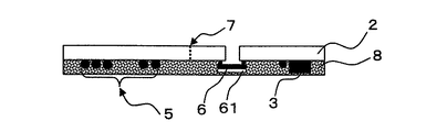
図1、図2に示すように、ICラベル1は、基材2の一方の面に設けられたICチップ(ICモジュール)と配線4を有する。配線4は、ICチップ((接続部図示せず)を有(図示せず)を有し、IC接続部を介してICチップと接続されている。基板の他方の面には粘着層8を備える。
また、配線4は、外部機器との非接触通信が可能なアンテナ部5と外部機器と接触通信を可能にするための外部端子部6とを有する。そして、配線は、アンテナ部と外部端子部の間に切取線を有する。この切取線はラベルを切り取る目安、ガイドとなるもので、切取線を有するため、切り取る前は非接触通信が可能で、切り取った後は接触通信が可能なICラベルとすることができる。
また、図4に示すように、基材の一方の面に配線4を設け、さらにその上に粘着層8を備えた構成をとることもできる。この場合、基材の外部端子部6に相当する部分に開口を設け、外部機器と接触通信を可能にすることができる。このようにすると、基材が保護層としての機能も有することができる。
Hereinafter, embodiments of the IC label according to the present invention will be described.
FIG. 1 is a schematic view of an
3 to 7 are sectional views showing other examples of the IC label.
As shown in FIGS. 1 and 2, the
Further, the
Moreover, as shown in FIG. 4, the structure which provided the
また、図3、5〜7に示すように配線4の上には、保護層9を設けても良い。保護層を設ける場合、配線4の外部端子部6が露出するよう、開口を設けることができる。開口を設けることにより、外部機器と接触通信が可能となる。
また、図5、6に示すようにこの保護フィルムの開口に外部端子保護シール11を設けても良い。外部端子保護シールを有することにより外部端子を使用する前又は使用しない時、外部端子を保護することができる。
さらに、図3、5〜7に示すように粘着層8上に剥離層10を設けても良い。
Further, as shown in FIGS. 3 and 5 to 7, a
Moreover, you may provide the external
Furthermore, you may provide the
基材2は、プラスチック基材や脆弱性基材を用いることができる。プラスチック基材としては、例えばアクリル系材料、ポリエステル系材料、ポリエチレンテレフタレート(PET)、ポリエチレンナフタレート(PEN)、ポリカーボネート(PC)などをあげることができる。
脆弱性基材としては、脆性プラスチック材料や紙材料が挙げられる。脆性プラスチック材料としては、例えば、カオリン、炭酸カルシウムなどの可塑剤を適量混合して脆質化した脆性塩化ビニル、脆性ポリエステルなどの合成樹脂フィルムや、又は、セルロースアセテート、低密度ポリエチレン、ポリスチレン、ポリフェニレンサルファイドなどの高結晶性プラスチック素材を溶液成膜により形成したフィルムなどがあげられる。紙材料としては、例えば上質紙や中質紙、微塗工紙、コート紙、アート紙、キャスト塗被紙、ガラス質の含浸紙、クラフト紙、合成紙などの紙類を使用することができる。脆弱性基材であれば、一度貼り付けた後にきれいに剥離することが困難であるため、不正な張替えを防ぐことができる。また、剥離時にアンテナを破壊して再利用を防ぐことも可能である。
As the
Examples of the brittle substrate include brittle plastic materials and paper materials. Examples of the brittle plastic material include, for example, a synthetic resin film such as brittle vinyl chloride and brittle polyester mixed with an appropriate amount of a plasticizer such as kaolin and calcium carbonate, or cellulose acetate, low density polyethylene, polystyrene, polyphenylene. Examples thereof include a film formed by forming a highly crystalline plastic material such as sulfide by solution film formation. Examples of paper materials that can be used include high-quality paper, medium-quality paper, fine-coated paper, coated paper, art paper, cast-coated paper, glass-impregnated paper, kraft paper, and synthetic paper. . If it is a fragile base material, it is difficult to peel it cleanly after being pasted once, so that unauthorized re-covering can be prevented. In addition, it is possible to prevent reuse by destroying the antenna at the time of peeling.
基材2は単層でもよいし、複数層積層したものを用いてもよい。
複数層積層したものとしては、例えば図7に示すように支持体22とICチップ、配線を設けたインレット基材21とを貼り合わせたものを用いても良い。基材は単層のものを用いる場合、おおよそ厚み50〜200μm程度であり、複数積層するものを用いる場合、各層が50〜100μm程度で総厚100〜200μm程度である。
支持体22は、基材2と同様のものを用いることができる。
インレット基材も基材2と同様のものを用いることができる。
インレット基材21と支持体22は接着剤により貼り合わせることができるが、材料によっては熱融着により貼り合わせても良い。
The
As what laminated | stacked multiple layers, you may use what bonded together the support body 22, the inlet base material 21 which provided the IC chip and the wiring, as shown in FIG. When a single-layer base material is used, the thickness is about 50 to 200 μm. When a plurality of base materials are used, each layer has a thickness of about 50 to 100 μm and a total thickness of about 100 to 200 μm.
The support 22 can be the same as the
The same inlet substrate as that of the
The inlet base material 21 and the support 22 can be bonded together with an adhesive, but depending on the material, they may be bonded together by heat fusion.
ICチップ3は、少なくとも接触通信機能と非接触通信機能を有するものを用い、配線に形成されたICチップ接続部(図示せず)を介して配線と接続される。
なお、ICチップ3は、基材上に設けても良いし、基材にICチップを収容するための凹部又は開口部を設けてそこに収容しても良い。
ICチップとしては、ICに接続用のバンプ(接続端子)を有するICチップ(いわゆるベアチップ)を用いることができる。また、接続板に実装したICチップ樹脂封止をしたいわゆるICモジュールを用いても良い。
ICチップ4のバンプは、電気的接合部を介してアンテナ3に電気的に接続されている。
電気的接合部としては、異方性導電ペースト(ACP)や異方性導電フィルム(ACF)等の金属粒子と接着剤バインダーから構成され、熱・圧力条件下における接着剤バインダーの硬化により電気的接続が実現されるものが好ましい。なお、配線のICチップ接続部とICチップ3の電気的接続は、上記したACPやACFを用いた接触接合方式に限定されず、例えば非導電性ペースト(NCP)や非導電性フィルム(NCF)を用いた接触接合方式であってもよく、さらには、超音波(USB)による金属接合方式であってもよい。
The
Note that the
As the IC chip, an IC chip (so-called bare chip) having connection bumps (connection terminals) on the IC can be used. Also, a so-called IC module sealed with an IC chip resin mounted on a connection plate may be used.
The bumps of the
The electrical joint is composed of metal particles such as anisotropic conductive paste (ACP) and anisotropic conductive film (ACF) and an adhesive binder, and is electrically connected by curing the adhesive binder under heat and pressure conditions. It is preferable that the connection is realized. Note that the electrical connection between the IC chip connection portion of the wiring and the
配線4は、ICチップ接続部、アンテナ部5、外部端子部6を有する。また、必要に応じてコンデンサ、マッチング回路などを備えていても良い。
配線4は、導電性材料により回路形成できるものであれば特に限定するものではなく様々なものを用いることができる。例えば、金属薄膜をエッチングによりパターン状に形成する方法や、導電性ワイヤーを配置する方法、導電性粒子を含むインキを印刷によりパターン状に形成したものなどが挙げられる。少なくともICチップ接続部、アンテナ部5は配線4と同様に形成することができ、外部端子部6は配線と同様に形成してよいが別に形成して接続してもよい。切り取り性を考慮すると、金属薄膜をエッチングによりパターン状に形成する方法、導電性粒子を含むインキを印刷によりパターン状に形成する方法を好ましく用いることができる。
配線の太さは特に限定するものではないが、0.05〜2mm程度のものを用いることができる。
The
The
The thickness of the wiring is not particularly limited, but a wiring having a thickness of about 0.05 to 2 mm can be used.
アンテナ部5は、外部の非接触通信用端末と通信が可能にすることができればよく、コイル状アンテナやダイポールアンテナ用の放射状アンテナを用いることができる。コイル状アンテナを用いる場合、後述する切取線により切取る前は、アンテナ部を介して外部端末と通信はできるものの外部端子部を介して外部端末と通信しようとしても回路的にショートしているため通信できないが、切取線により切取った後は、アンテナ部がなくなるため非接触通信はできなくなるものの外部端子部を介して外部端末と通信が可能となる。なお、コイルアンテナの巻数は目的に応じて任意に設定できる。
放射状アンテナを用いる場合、後述する切取線により切取る前は、アンテナ部を介した外部端末との通信と外部端子部を介した外部端末との通信が可能である。切取線により切取った後は、アンテナ部がなくなるため非接触通信の場合は通信距離が著しく短くなる又は通信が不能となるが、外部端子部を介した外部端末との通信は可能となる。
The
When a radial antenna is used, communication with an external terminal through the antenna unit and communication with an external terminal through the external terminal unit are possible before cutting with a cutoff line described later. After being cut off by the cut line, the antenna portion is eliminated, and in the case of non-contact communication, the communication distance is remarkably shortened or communication is impossible, but communication with an external terminal via the external terminal portion is possible.
金属薄膜をエッチングによりパターン状に形成する方法としては、基材2又はインレット基材21にアルミや銅、銀、錫などの金属薄膜を形成したものを用い、回路パターン状のマスク層を形成し、エッチング液によりマスク層が形成された部分以外の金属薄膜を除去することにより、金属薄膜の配線パターンを得ることができる。
この方法を用いる場合、基材2上に直接配線を設けるのであれば、基材2はエッチング耐性のあるプラスチックフィルムを好適に用いることができる。また、インレット基材21上に設けるのであれば、インレット基材21エッチング耐性のあるプラスチックフィルムを好適に用いることができ、支持体としては、プラスチック基材や脆弱性基材を用いることができる。
なお、この方法によりコイル状のアンテナ部を形成する場合、コイル最内周から外部端子部への接続用のジャンパー線を引き出しても良い。ジャンパー線は線状の金属薄膜の両端以外を絶縁層を設け、両端部を配線に接触させる方法や、基材又はインレット基材の配線を設けた面とは反対の面に金属薄膜パターンを設け、基材又はインレット基材を貫通するスルーホールに導電材料を設けて接続させる方法がある。
As a method of forming a metal thin film into a pattern by etching, a circuit pattern-like mask layer is formed using a
When this method is used, if wiring is directly provided on the
In addition, when forming a coil-shaped antenna part by this method, you may draw out the jumper wire for connection to an external terminal part from a coil innermost periphery. For the jumper wire, an insulating layer is provided on both sides of the linear metal thin film, and both ends are in contact with the wiring, or a metal thin film pattern is provided on the surface opposite to the surface on which the wiring of the base material or inlet base material is provided. There is a method in which a conductive material is provided and connected to a through hole penetrating the base material or the inlet base material.
導電性ワイヤーを配置する方法は、金属線などの導電性の線材を巻き線機等により基材、インレット基材に配することができる。
導電性の線材としては、銅、アルミ、銀、金、鉄、錫などの金属材料からなる線材を用いることができる。また、絶縁材料で被覆したものを用いても良い。絶縁材料で被覆することによりコイル最内周から外部端子部へコイルを跨いで配置することができ、ジャンパー線を用いなくてもよいものとなる。
As a method of arranging the conductive wire, a conductive wire such as a metal wire can be arranged on the base material or the inlet base material by a winding machine or the like.
As the conductive wire, a wire made of a metal material such as copper, aluminum, silver, gold, iron, or tin can be used. Moreover, you may use what was coat | covered with the insulating material. By covering with an insulating material, the coil can be disposed across the coil from the innermost periphery of the coil to the external terminal portion, and a jumper wire need not be used.
導電性粒子を含むインキを用いる方法は、銀ペーストなどの、導電性粒子、溶剤、バインダー樹脂等を含むインキを印刷法によりパターン形成する方法である。導電性粒子としては、銀、銅、ニッケルや錫などの金属粒子や、導電性カーボン粉末、導電性繊維、導電性ウィスカーなどが上げられる。溶剤としては、特に限定するものではなく、粒子等の相性を考慮し選ぶことができる。樹脂バインダーは、必要に応じて加えることができる。
印刷法としては、スクリーン印刷、フレキソ印刷、グラビア印刷、オフセット印刷、インクジェット法などの印刷方式で印刷して形成することができる。この方法で形成した配線は、基材から剥がれ易くなり破壊され易いため、ICラベルの使い廻しを防ぐことができる。
なお、この方法によりコイル状のアンテナ部を形成する場合、コイル最内周から外部端子部への接続用のジャンパー線を引き出しても良い。ジャンパー線は線状の金属薄膜の両端以外を絶縁層を設け、両端部を配線に接触させる方法や、基材又はインレット基材の配線を設けた面とは反対の面に導電パターンを設け、基材又はインレット基材を貫通するスルーホールに導電材料を設けて接続させる方法がある。
The method using an ink containing conductive particles is a method of patterning an ink containing conductive particles, a solvent, a binder resin, etc., such as a silver paste, by a printing method. Examples of the conductive particles include metal particles such as silver, copper, nickel, and tin, conductive carbon powder, conductive fibers, and conductive whiskers. The solvent is not particularly limited and can be selected in consideration of the compatibility of particles and the like. The resin binder can be added as necessary.
As a printing method, it can be formed by printing by a printing method such as screen printing, flexographic printing, gravure printing, offset printing, or inkjet method. Since the wiring formed by this method is easily peeled off from the base material and easily broken, it is possible to prevent the IC label from being reused.
In addition, when forming a coil-shaped antenna part by this method, you may draw out the jumper wire for connection to an external terminal part from a coil innermost periphery. The jumper wire is provided with an insulating layer other than both ends of the linear metal thin film, and a method of bringing both ends into contact with the wiring, or a conductive pattern on the surface opposite to the surface on which the wiring of the base material or the inlet base material is provided, There is a method in which a conductive material is provided and connected to a through hole penetrating a base material or an inlet base material.
外部端子部6は、金属薄膜をエッチングによりパターン状に形成する方法、導電性粒子を含むインキを用いる方法で配線を形成する場合、配線の形成と同時に形成することができる。この場合外部端子部6は接触用の外部端末の端子が来る位置に対し、端子の大きさに合わせて形成することができる。例えば外部端末機器側の端子部と接触しやすくなるように、配線に対し外部端子部6を幅広に形成することができる。外部端子部6は例えば、0.5×0.5mm〜5×5mm程度の大きさで形成することができる。
外部端末機器側の端子部の大きさ・形状によっては、配線の線上を外部端子部と兼用しても良い。また、外部端子部はメッキなどを施すことができる。メッキを施すことで、接触不良の低減や耐久性向上を図ることができ、接続信頼性を向上させることができる。メッキを施す材料としては、金、銀、ニッケルまたはこれらの合金等を用いることができる。
また、配線の形成と同時に形成せず、導電部材を外部端子部として配線上に配置してもよい。
また、図4に示すように、基材に開口を設け、開口から外部端子6を露出させる場合は、基材裏面の開口近くまで配線を設け、支持体に導電材料を設けた導電部材を開口に設けて配線と接続することにより、外部端子6を設けることができる。
The external
Depending on the size and shape of the terminal portion on the external terminal device side, the wiring line may also be used as the external terminal portion. The external terminal portion can be plated. By plating, contact failure can be reduced and durability can be improved, and connection reliability can be improved. As a material to be plated, gold, silver, nickel, or an alloy thereof can be used.
Further, the conductive member may be arranged on the wiring as an external terminal portion without being formed simultaneously with the formation of the wiring.
In addition, as shown in FIG. 4, when an opening is provided in the base material and the
導電性ワイヤーを配置する方法で配線を形成する場合、導電部材を外部端子部として配線上に配置することにより、外部端子部を形成することができる。
導電部材としては金属薄膜を転写形成する方法や、印刷法により導電性材料を形成するしてもよい。外部端子部6は接触用の外部端末の端子が来る位置に対し、端子の大きさに合わせて形成することができる。例えば外部端末機器側の端子部と接触しやすくなるように、配線に対し外部端子部6を幅広に形成することができる。また、外部端子部にはメッキなどを施すことができる。メッキを施すことで、接触不良の低減や耐久性向上を図ることができる。メッキを施す材料としては、金、銀、ニッケル等を用いることができる。
また、外部端末機器の端子部の大きさ・形状によっては、導電性ワイヤーからなる配線の線上を外部端子部と兼用しても良い。
また、図4に示すように、基材に開口を設け、開口から外部端子6を露出させる場合は、基材裏面の開口近くまで配線を設け、導電部材を開口に設けて配線と接続することにより、外部端子6を設けることができる。
When the wiring is formed by the method of disposing the conductive wire, the external terminal portion can be formed by disposing the conductive member on the wiring as the external terminal portion.
As the conductive member, a conductive material may be formed by transferring a metal thin film or printing. The external
Further, depending on the size and shape of the terminal portion of the external terminal device, the wiring line made of the conductive wire may be used also as the external terminal portion.
In addition, as shown in FIG. 4, when an opening is provided in the base material and the
基材のアンテナ、ICチップ等を設けた面とは反対の面には粘着層(又は接着層)を設けることができる。粘着層としては、例えばアクリル系材料、ウレタン系材料、エポキシ系材料、エチレン−酢酸ビニル樹脂などを用いることができる。
粘着層はラベルの全面に設けても良いし、折線を挟んでICチップ側のみに設けても良い。
An adhesive layer (or adhesive layer) can be provided on the surface of the substrate opposite to the surface provided with the antenna, IC chip, or the like. As the adhesive layer, for example, an acrylic material, a urethane material, an epoxy material, an ethylene-vinyl acetate resin, or the like can be used.
The pressure-sensitive adhesive layer may be provided on the entire surface of the label, or may be provided only on the IC chip side with a folding line interposed therebetween.
本発明では剥離層10を設けても良い。剥離層は貼り付け時に剥がして使用する。剥離層10としては、紙製又はプラスチック製のシートにシリコン樹脂などの離型剤層がコーティングなどによって積層されているセパレータが用いられる。
In the present invention, the
本発明では、基材のICチップ、配線を形成した面上に保護層9を設けることができる。保護層は、アクリル系、ポリエステル系、セルロース系等のフィルム材料や紙材料等のシート材料を、貼り合わせ又は転写形成することができる。また、アクリル系樹脂、ポリエステル系樹脂、ウレタン系樹脂などの樹脂材料を塗布することにより設けても良い。フィルムを転写形成する場合は、ホログラム加工を施したフィルムを転写形成してもよい。
保護層9は、外部端子部を露出するように形成する。シート材料を貼り合わせ、転写形成する場合は、外部端子部に相当する部分に開口を設け、位置合わせを行い貼り合わせ、転写することで形成できる。樹脂材料を塗布する場合は、印刷法などにより外部端子部を避けて印刷することにより形成できる。保護層9の開口部は外部端子部のうち、少なくとも外部端末と接触する部分が露出されていれば良く、おおよそ外部端子部の面積に対し、80〜200%程度露出していればよい。
また、保護層9の厚みとしては、0.1〜1000μm程度の範囲内で適宜設定できるがこれに限られるものではない。
また、保護層は、透明のものを用いても良いが、配線を隠蔽することができる有色のものを用いても良い。隠蔽性を有することで回路パターンの流出を防ぐことができる。
また、保護層は、ラベル基材として機能してもよい。
In the present invention, the
The
Moreover, as thickness of the
Further, the protective layer may be transparent, but may be a colored layer that can conceal the wiring. The circuit pattern can be prevented from flowing out by having concealment.
The protective layer may function as a label base material.
保護層9の外部端子が露出した開口部分には、外部端子保護シールを設けても良い。外部端子保護シールを設けることで、外部端末と接触通信させる前又は接触通信をしない時、外部端子部を保護することができる。外部端子保護シールは図5に示すように保護層の開口内に設けても良いし、図6に示すように開口を覆うように設けても良い。
外部端子保護シールとしては、PET等のポリエステル系材料、アクリル系材料、紙材料などからなる保護シール基材と、アクリル系材料、ウレタン系材料、エポキシ系材料、エチレン−酢酸ビニル樹脂などの粘着剤を有するものを用いることができる。
また剥がしやすいように必要に応じてラベル側に易剥離層を形成してもよい。
You may provide an external terminal protection seal in the opening part which the external terminal of the
As external terminal protective seals, protective seal substrates made of polyester materials such as PET, acrylic materials, paper materials, etc., and adhesives such as acrylic materials, urethane materials, epoxy materials, ethylene-vinyl acetate resins, etc. The thing which has can be used.
Moreover, you may form an easy peeling layer in the label side as needed so that it may peel easily.
本発明のICラベルは基材2のアンテナ部5を設けた部分と外部端子部6を設けた部分の間に切取線7を有することを特徴とする。切取線7はアンテナ部5と外部端子6を繋ぐ配線4を横切りラベルを分割できるような形状であれば、直線、曲線またはその組み合わせなどを用いることができる。
切取線7はICラベルに用いる基材、保護層の材質に応じて設けることができ、例えば切取の目安となる線、切取やすくするための片側又は両側から形成した線状の凹部、片側又は両側からの線状のハーフカット、ミシン目などを用いることができる。
The IC label according to the present invention is characterized in that a cut line 7 is provided between a portion of the
The cut line 7 can be provided according to the base material used for the IC label and the material of the protective layer. For example, a line serving as a guide for cutting, a linear recess formed from one side or both sides for easy cutting, from one side or both sides A linear half cut, perforation, or the like can be used.
切取線はICラベルを切り取りしやすくなるように設ければよい。
目安となる線は、印刷、印字などにより基材とは異なる色相の線を設けるものである。基材が紙材などからなる場合はこの方法を用いることができる。特に繊維の方向が揃っている場合等は繊維の方向に沿って目安となる線を設けておくことで線に沿ってきれいに切り取ることができる。
凹部は線材などにより押圧することで設けることができる。線状の凹部を設ける場合は、ラベルの総厚に対し、5〜50%程度の厚みになるような凹部をラベルの片側または両側から押圧により形成することができる。保護層を有する場合、基材と保護層の各々に凹部を設け位置合わせをして貼り合わせてもよいし、最上層となる保護層のみに凹部を設けても良い。また、粘着層を設ける前に形成してもよいし粘着層を形成した後に粘着層上から押圧してもよい。
ハーフカットは刃材を用いて基材断面方向において途中まで切り込みを入れることで設けることができる。線状のハーフカットを設ける場合は、ラベルの総厚に対し、5〜50%程度の厚みになるような切込みをラベルの片側または両側から形成することができる。保護層を有する場合、保護層側は保護層から基材へ切れ込みを入れてもよいし、保護層のみに切れ込みを設けても良い。この場合、基材の保護層とは反対側に切れ込みを入れても良い。また、粘着層を設ける前に形成してもよいし粘着層を形成した後に粘着層上から切り込みを入れてもよい。
ミシン目は一定の間隔で孔を形成する。ミシン目を設ける場合は、貫通孔、非貫通孔のいずれを用いてもかまわない。保護層を有する場合、保護層と基材の双方にミシン目を入れても良いし保護層のみにミシン目を設けてもよい。また、粘着層を設ける前に形成してもよいし粘着層を形成した後に粘着層上から切り込みを入れてもよい。
また、保護層を有する場合、基材のみに凹部、ハーフカット、ミシン目を設けてもよい。この場合保護層上には必要に応じて目安となる線を設けてもよい。保護層が比較的薄い紙材である場合はこのような構成をとることができる。
The cut line may be provided so that the IC label can be easily cut.
The reference line is a line having a hue different from that of the substrate by printing, printing, or the like. This method can be used when the substrate is made of paper. In particular, when the directions of the fibers are aligned, for example, by providing a reference line along the direction of the fiber, it can be cut out cleanly along the line.
The recess can be provided by pressing with a wire or the like. When providing a linear recessed part, the recessed part which becomes a thickness of about 5 to 50% with respect to the total thickness of a label can be formed by pressing from the one side or both sides of a label. In the case where the protective layer is provided, a concave portion may be provided on each of the base material and the protective layer for alignment, or the concave portion may be provided only on the uppermost protective layer. Moreover, you may form before providing an adhesion layer, and you may press from on an adhesion layer after forming an adhesion layer.
Half-cutting can be provided by cutting halfway in the substrate cross-sectional direction using a blade material. In the case of providing a linear half cut, it is possible to form a cut from one side or both sides of the label so as to be about 5 to 50% of the total thickness of the label. When the protective layer is provided, the protective layer side may be cut from the protective layer to the base material, or may be provided only on the protective layer. In this case, a cut may be made on the side of the substrate opposite to the protective layer. Moreover, you may form before providing an adhesion layer, and you may make a notch | incision from the adhesion layer after forming an adhesion layer.
Perforations form holes at regular intervals. When the perforation is provided, either a through hole or a non-through hole may be used. When the protective layer is provided, perforations may be provided in both the protective layer and the substrate, or perforations may be provided only in the protective layer. Moreover, you may form before providing an adhesion layer, and you may make a notch | incision from the adhesion layer after forming an adhesion layer.
Moreover, when it has a protective layer, you may provide a recessed part, a half cut, and a perforation only in a base material. In this case, a reference line may be provided on the protective layer as necessary. Such a configuration can be adopted when the protective layer is a relatively thin paper material.
また、切取線は、配線が形成されている部分を避けるように、すなわち配線が形成されてない部分に設けることができる。切取線としてハーフカット、凹部、ミシン目を用いる場合、これらを配線部分に形成すると電気的に切断される可能性がある。そのため、配線が形成されている部分は切り取り線を設けないようにすることで、配線の断線を防ぐことが出来る。 Further, the cutoff line can be provided so as to avoid a portion where the wiring is formed, that is, a portion where the wiring is not formed. When half cuts, recesses, and perforations are used as the cut lines, there is a possibility of electrical disconnection if these are formed in the wiring portion. Therefore, disconnection of the wiring can be prevented by not providing a cut line in the portion where the wiring is formed.
また、基材のICチップ、配線を形成した面とは反対の面に溶剤発色層(溶剤検出部)を設けてもよい。溶剤発色層は、被貼付体に貼り付けられたICラベルを剥離するための剥離溶剤と化学反応する性質のものからなる。剥離溶剤としては、エチルアルコールやアセトンなどの溶解性の弱い有機溶剤や市販のシール剥し液などがある。溶剤発色層は、水不溶性で且つ剥離溶剤に対し可溶性の染料粒子を樹脂バインダー中に体質顔料等と分散状態で保持した構造をとる。これにより、剥離溶剤を用いてICラベルの剥離を試みると、溶剤発色層に分散状態で保持した顔料が溶解し、基材に発色として痕跡が残る。なお、染料粒子としては、例えばロイコ染料や蛍光増白剤等の染料を使用することができる。
また、上述したような剥離溶剤で剥がす行為以外に、ドライヤなどの熱で粘着層の粘着材を軟化させてICラベルを剥がすことが想定される。この場合、上記した染料だけでは溶融する温度まで至らず効果が不十分である。そこで、溶剤発色層の材料に、熱刺激により発色するサーマル発色材料を使用することが好ましい。例えば、ロイコ染料と合わせて、熱刺激によってロイコ染料と結合する顕色剤を分散させる。この場合、ロイコ染料は通常無色か淡色の材料が使用され、サーマルで反応した際に色調として顕在化するものが適している。これにより、溶剤発色層がサーマル発色機能を有し、熱で接着層を軟化させて剥がそうとすると、溶剤発色層が発色して痕跡が残る。なお、溶剤発色層は、上記した溶剤発色機能又はサーマル発色機能の少なくとも一方の機能を有していればよい。
また、上記した溶剤発色層に代えて、剥離溶剤に溶解する溶剤溶解層(溶剤検出部)を設けてもよい。これにより、剥離溶剤を用いてICラベルの剥離を試みると、剥離溶剤によって溶剤溶解層が溶解し、基材に痕跡が残る。なお、上記した溶剤発色層及び溶剤溶解層をそれぞれ設けてもよい。これにより、より確実に剥離の痕跡が残る。
Further, a solvent coloring layer (solvent detector) may be provided on the surface opposite to the surface on which the IC chip and the wiring are formed. The solvent coloring layer has a property of chemically reacting with a peeling solvent for peeling the IC label attached to the adherend. Examples of the stripping solvent include weakly soluble organic solvents such as ethyl alcohol and acetone, and commercially available seal strippers. The solvent coloring layer has a structure in which dye particles that are insoluble in water and soluble in the peeling solvent are held in a dispersed state with an extender pigment in a resin binder. As a result, when the IC label is peeled off using a peeling solvent, the pigment held in a dispersed state in the solvent coloring layer is dissolved, and a trace remains as a color on the substrate. In addition, as dye particle | grains, dyes, such as a leuco dye and a fluorescent whitening agent, can be used, for example.
In addition to the action of peeling with a peeling solvent as described above, it is assumed that the adhesive material of the pressure-sensitive adhesive layer is softened by heat of a dryer or the like to peel off the IC label. In this case, the above-described dye alone does not reach the melting temperature, and the effect is insufficient. Therefore, it is preferable to use a thermal coloring material that develops color by thermal stimulation as the material of the solvent coloring layer. For example, together with the leuco dye, a developer that binds to the leuco dye by thermal stimulation is dispersed. In this case, a leuco dye is usually a colorless or light-colored material, and a material that manifests as a color tone when reacted with thermal is suitable. As a result, the solvent coloring layer has a thermal coloring function, and when the adhesive layer is softened and peeled off by heat, the solvent coloring layer is colored and a trace remains. In addition, the solvent coloring layer should just have at least one function of the above-mentioned solvent coloring function or thermal coloring function.
Moreover, it may replace with the above-mentioned solvent coloring layer, and you may provide the solvent melt | dissolution layer (solvent detection part) which melt | dissolves in a peeling solvent. Thereby, when peeling of an IC label is attempted using a peeling solvent, the solvent-dissolved layer is dissolved by the peeling solvent, and a trace remains on the substrate. In addition, you may provide the above-mentioned solvent coloring layer and solvent melt | dissolution layer, respectively. Thereby, the trace of peeling remains more reliably.
また、本発明のICラベルには各層の層間または層上に赤外線吸収材料又は蛍光材料等の発光材料などの不可視セキュリティインキによるセキュリティ印刷層を設けても良い。セキュリティ印刷層は固有番号などを印刷することができる。 Further, the IC label of the present invention may be provided with a security printing layer made of an invisible security ink such as an infrared absorbing material or a light emitting material such as a fluorescent material between or on each layer. The security printing layer can print a unique number or the like.
また、本発明では必要に応じて絵柄層、印字層などを設けることができる。
さらに配線を隠蔽する隠蔽層を設けても良い。隠蔽層としては、有色の顔料、染料を含むインキを塗布することにより形成できる。
In the present invention, a picture layer, a printing layer, and the like can be provided as necessary.
Further, a concealing layer for concealing the wiring may be provided. The hiding layer can be formed by applying an ink containing a colored pigment or dye.
基材として厚み50μmのPETフィルムを用い、この基材の一方の面に銅をエッチングした配線を形成した。配線の厚みは10μm、線幅は0.5mmとした。配線パターンは図1のようにし、ICチップ接続部(図示せず)、外部端子部、アンテナ部を形成した。なお、外部端子部は1.5×4mmの大きさで2つ形成し、アンテナ部は3ターンのコイルアンテナとした。
次に、配線のICチップ接続部に接触通信と非接触通信が可能なデュアルICチップを接続した。
次に、保護層として外部端子部に合わせて1.5×4mmの開口部を2つ形成した紙基材を用意し、開口部と基材に形成された外部端子の位置を合わせてアクリル系接着剤で貼り合わせた。
次にアンテナ部と外部端子部の間に、カット部2mm、ピッチ1mmからなるミシン目を形成した。
最後に、基材の配線を形成した側とは反対側にアクリル系接着剤、剥離紙を設け、実施例のICラベルを得た。
A PET film having a thickness of 50 μm was used as a base material, and a wiring obtained by etching copper was formed on one surface of the base material. The wiring thickness was 10 μm and the line width was 0.5 mm. The wiring pattern was as shown in FIG. 1, and an IC chip connection part (not shown), an external terminal part, and an antenna part were formed. Two external terminal portions having a size of 1.5 × 4 mm were formed, and the antenna portion was a three-turn coil antenna.
Next, a dual IC chip capable of contact communication and non-contact communication was connected to the IC chip connection portion of the wiring.
Next, a paper base material having two 1.5 × 4 mm openings formed in accordance with the external terminal portion as a protective layer is prepared, and the acrylic resin is prepared by aligning the positions of the openings and the external terminals formed on the base material. It bonded together with the adhesive agent.
Next, a perforation having a cut portion of 2 mm and a pitch of 1 mm was formed between the antenna portion and the external terminal portion.
Finally, an acrylic adhesive and release paper were provided on the side of the substrate opposite to the side on which the wiring was formed to obtain an IC label of the example.
<評価>
非接触式のR/Wと接触式のR/Wを用いて、実施例1のICラベルとの通信状態を確認した。
結果、ICラベルをミシン目に沿って切り取る前は、非接触式R/Wとは良好に通信できたが、接触式R/Wとの通信はできなかった。ICラベルをミシン目に沿って切り取った後は、非接触式R/Wとの通信はできず、接触式R/Wとの通信は良好にできた。
<Evaluation>
Using the non-contact type R / W and the contact type R / W, the communication state with the IC label of Example 1 was confirmed.
As a result, before the IC label was cut along the perforation, communication with the non-contact type R / W was successfully performed, but communication with the contact type R / W was not possible. After the IC label was cut off along the perforation, communication with the non-contact type R / W was not possible, and communication with the contact type R / W was good.
1・・・・ICラベル
2・・・・基材
21・・・インレット基材
22・・・支持体
3・・・・ICチップ
4・・・・配線
5・・・・アンテナ部
6・・・・外部端子部
61・・・支持体
7・・・・切取線
8・・・・粘着層
9・・・・保護層
10・・・剥離層
11・・・外部端子保護シール
12・・・粘着層
13・・・保護シール基材
DESCRIPTION OF
Claims (7)
該配線が、ICチップと接続するためのICチップ接続部とアンテナ部を有し、さらにICチップ接続部とアンテナ部の間に外部端子部を有し、
アンテナ部と外部端子部の間に切取線を有することを特徴とするICラベル。 A substrate, an IC chip, wiring connected to the IC chip, and an adhesive layer;
The wiring has an IC chip connection part and an antenna part for connecting to the IC chip, and further has an external terminal part between the IC chip connection part and the antenna part,
An IC label comprising a cut line between an antenna portion and an external terminal portion.
該保護層が外部端子を露出する開口部を有することを特徴とする請求項1記載のICラベル。 A protective layer on the IC chip and the wiring;
2. The IC label according to claim 1, wherein the protective layer has an opening for exposing the external terminal.
Priority Applications (1)
| Application Number | Priority Date | Filing Date | Title |
|---|---|---|---|
| JP2012071351A JP2013205902A (en) | 2012-03-27 | 2012-03-27 | Ic label |
Applications Claiming Priority (1)
| Application Number | Priority Date | Filing Date | Title |
|---|---|---|---|
| JP2012071351A JP2013205902A (en) | 2012-03-27 | 2012-03-27 | Ic label |
Publications (1)
| Publication Number | Publication Date |
|---|---|
| JP2013205902A true JP2013205902A (en) | 2013-10-07 |
Family
ID=49524970
Family Applications (1)
| Application Number | Title | Priority Date | Filing Date |
|---|---|---|---|
| JP2012071351A Pending JP2013205902A (en) | 2012-03-27 | 2012-03-27 | Ic label |
Country Status (1)
| Country | Link |
|---|---|
| JP (1) | JP2013205902A (en) |
Cited By (1)
| Publication number | Priority date | Publication date | Assignee | Title |
|---|---|---|---|---|
| KR20220033910A (en) * | 2020-09-10 | 2022-03-17 | 김영집 | Tape type rf-tag for access to security facilities |
Citations (6)
| Publication number | Priority date | Publication date | Assignee | Title |
|---|---|---|---|---|
| JPH08267974A (en) * | 1995-03-31 | 1996-10-15 | Tokai Rika Co Ltd | Ic card |
| JP2000090224A (en) * | 1998-09-14 | 2000-03-31 | Toshiba Corp | Information processing medium |
| JP2002230509A (en) * | 2001-01-30 | 2002-08-16 | J-Phone East Co Ltd | Ic card |
| EP1308886A2 (en) * | 2001-11-06 | 2003-05-07 | Quadnovation, Inc. | Contactless transaction card with separable antenna and carrier therefor |
| JP2005284517A (en) * | 2004-03-29 | 2005-10-13 | Toppan Forms Co Ltd | Rfid type sheet |
| EP2264649A2 (en) * | 2003-07-07 | 2010-12-22 | Avery Dennison Corporation | RFID device with changeable characteristics |
-
2012
- 2012-03-27 JP JP2012071351A patent/JP2013205902A/en active Pending
Patent Citations (6)
| Publication number | Priority date | Publication date | Assignee | Title |
|---|---|---|---|---|
| JPH08267974A (en) * | 1995-03-31 | 1996-10-15 | Tokai Rika Co Ltd | Ic card |
| JP2000090224A (en) * | 1998-09-14 | 2000-03-31 | Toshiba Corp | Information processing medium |
| JP2002230509A (en) * | 2001-01-30 | 2002-08-16 | J-Phone East Co Ltd | Ic card |
| EP1308886A2 (en) * | 2001-11-06 | 2003-05-07 | Quadnovation, Inc. | Contactless transaction card with separable antenna and carrier therefor |
| EP2264649A2 (en) * | 2003-07-07 | 2010-12-22 | Avery Dennison Corporation | RFID device with changeable characteristics |
| JP2005284517A (en) * | 2004-03-29 | 2005-10-13 | Toppan Forms Co Ltd | Rfid type sheet |
Cited By (2)
| Publication number | Priority date | Publication date | Assignee | Title |
|---|---|---|---|---|
| KR20220033910A (en) * | 2020-09-10 | 2022-03-17 | 김영집 | Tape type rf-tag for access to security facilities |
| KR102469022B1 (en) * | 2020-09-10 | 2022-11-21 | 김영집 | Tape type rf-tag for access to security facilities |
Similar Documents
| Publication | Publication Date | Title |
|---|---|---|
| JP5923624B2 (en) | Fragile high-frequency RFID electronic tag having a transfer prevention function and manufacturing method thereof | |
| US7872579B2 (en) | Structure including an electronic device, in particular for fabricating a security document or a document of value | |
| EP1505537B1 (en) | Ic tag | |
| JP6136100B2 (en) | ink cartridge | |
| JP3854124B2 (en) | Non-contact IC label | |
| JP2013205903A (en) | Ic label | |
| JP4675184B2 (en) | IC tag | |
| JP6136099B2 (en) | ink cartridge | |
| JP2012230469A (en) | Noncontact ic label | |
| JP2013205902A (en) | Ic label | |
| JP5862037B2 (en) | Brittle RFID label | |
| JP4736555B2 (en) | Information recording medium | |
| JP4127650B2 (en) | IC tag | |
| JP2015060504A (en) | Non-contact ic label | |
| JP5375649B2 (en) | Non-contact IC label | |
| JP5569347B2 (en) | RFID label | |
| JP2008078337A (en) | Connecting part for conductor pattern, and connecting structure thereof | |
| JP5375648B2 (en) | Non-contact IC label | |
| JP2012150538A (en) | Rfid label | |
| JP2008097525A (en) | Ic tag sheet | |
| JP2016042206A (en) | Brittle RFID label | |
| JP2018036417A (en) | Transfer-type security label sheet, method for attaching security label, and security label | |
| JP2023113073A (en) | Ic card laminate and manufacturing method for ic card laminate | |
| CN113487005A (en) | Method for preventing secondary chip transfer and chip thereof | |
| JP5929032B2 (en) | Booklet with IC |
Legal Events
| Date | Code | Title | Description |
|---|---|---|---|
| A621 | Written request for application examination |
Free format text: JAPANESE INTERMEDIATE CODE: A621 Effective date: 20150219 |
|
| A977 | Report on retrieval |
Free format text: JAPANESE INTERMEDIATE CODE: A971007 Effective date: 20151218 |
|
| A131 | Notification of reasons for refusal |
Free format text: JAPANESE INTERMEDIATE CODE: A131 Effective date: 20160105 |
|
| A521 | Written amendment |
Free format text: JAPANESE INTERMEDIATE CODE: A523 Effective date: 20160301 |
|
| A02 | Decision of refusal |
Free format text: JAPANESE INTERMEDIATE CODE: A02 Effective date: 20160517 |