JP2013003238A - Video signal processing circuit, video signal processing method, display device, and electronic apparatus - Google Patents
Video signal processing circuit, video signal processing method, display device, and electronic apparatus Download PDFInfo
- Publication number
- JP2013003238A JP2013003238A JP2011132006A JP2011132006A JP2013003238A JP 2013003238 A JP2013003238 A JP 2013003238A JP 2011132006 A JP2011132006 A JP 2011132006A JP 2011132006 A JP2011132006 A JP 2011132006A JP 2013003238 A JP2013003238 A JP 2013003238A
- Authority
- JP
- Japan
- Prior art keywords
- video signal
- frame
- control
- signal processing
- integrated value
- Prior art date
- Legal status (The legal status is an assumption and is not a legal conclusion. Google has not performed a legal analysis and makes no representation as to the accuracy of the status listed.)
- Pending
Links
Images


Classifications
-
- G—PHYSICS
- G09—EDUCATION; CRYPTOGRAPHY; DISPLAY; ADVERTISING; SEALS
- G09G—ARRANGEMENTS OR CIRCUITS FOR CONTROL OF INDICATING DEVICES USING STATIC MEANS TO PRESENT VARIABLE INFORMATION
- G09G3/00—Control arrangements or circuits, of interest only in connection with visual indicators other than cathode-ray tubes
- G09G3/20—Control arrangements or circuits, of interest only in connection with visual indicators other than cathode-ray tubes for presentation of an assembly of a number of characters, e.g. a page, by composing the assembly by combination of individual elements arranged in a matrix no fixed position being assigned to or needed to be assigned to the individual characters or partial characters
-
- G—PHYSICS
- G09—EDUCATION; CRYPTOGRAPHY; DISPLAY; ADVERTISING; SEALS
- G09G—ARRANGEMENTS OR CIRCUITS FOR CONTROL OF INDICATING DEVICES USING STATIC MEANS TO PRESENT VARIABLE INFORMATION
- G09G2320/00—Control of display operating conditions
- G09G2320/06—Adjustment of display parameters
- G09G2320/0626—Adjustment of display parameters for control of overall brightness
-
- G—PHYSICS
- G09—EDUCATION; CRYPTOGRAPHY; DISPLAY; ADVERTISING; SEALS
- G09G—ARRANGEMENTS OR CIRCUITS FOR CONTROL OF INDICATING DEVICES USING STATIC MEANS TO PRESENT VARIABLE INFORMATION
- G09G2330/00—Aspects of power supply; Aspects of display protection and defect management
- G09G2330/02—Details of power systems and of start or stop of display operation
- G09G2330/021—Power management, e.g. power saving
-
- G—PHYSICS
- G09—EDUCATION; CRYPTOGRAPHY; DISPLAY; ADVERTISING; SEALS
- G09G—ARRANGEMENTS OR CIRCUITS FOR CONTROL OF INDICATING DEVICES USING STATIC MEANS TO PRESENT VARIABLE INFORMATION
- G09G2360/00—Aspects of the architecture of display systems
- G09G2360/16—Calculation or use of calculated indices related to luminance levels in display data
Abstract
Description
本開示は、映像信号処理回路、映像信号処理方法、表示装置、及び、電子機器に関し、特に、映像信号の輝度制御を行う映像信号処理回路、映像信号処理方法、当該映像信号処理回路を備える表示装置、及び、当該表示装置を有する電子機器に関する。 The present disclosure relates to a video signal processing circuit, a video signal processing method, a display device, and an electronic device, and in particular, a video signal processing circuit that performs luminance control of a video signal, a video signal processing method, and a display including the video signal processing circuit. The present invention relates to a device and an electronic device including the display device.
表示装置において、高輝度の映像信号が入力された場合に、表示パネルに入力する映像信号を制御し、画素の電気光学素子に流れる電流を抑えることで、消費電流(消費電力)の低減を図ることができる。 In a display device, when a high-luminance video signal is input, the video signal input to the display panel is controlled to suppress current flowing through the electro-optical element of the pixel, thereby reducing current consumption (power consumption). be able to.
かかる制御を行う映像信号処理回路では、従来、入力される映像信号を基に1画面(1フレーム)毎に輝度積算値を算出し、この算出した輝度積算値に基づいて映像信号の振幅を制御し、その振幅制御後の映像信号を表示装置に供給するようにしていた(例えば、特許文献1参照)。 In a video signal processing circuit that performs such control, conventionally, a luminance integrated value is calculated for each screen (one frame) based on an input video signal, and the amplitude of the video signal is controlled based on the calculated luminance integrated value. However, the video signal after the amplitude control is supplied to the display device (see, for example, Patent Document 1).
上記の従来技術に係る映像信号処理回路では、入力される映像信号から1フレーム毎に輝度積算値を算出し、その算出結果を基に映像信号の輝度制御を行うようにしている。これにより、前フレームの算出結果が現フレームの制御に反映されるため、算出結果が輝度制御に反映されるのに必ず1フレーム相当の時間の遅延が生じる。従って、輝度積算値を算出する1フレームの期間は、映像信号の輝度制御、即ち、消費電流低減のための制御が行えないことになる。 In the video signal processing circuit according to the above prior art, the luminance integrated value is calculated for each frame from the input video signal, and the luminance control of the video signal is performed based on the calculation result. As a result, since the calculation result of the previous frame is reflected in the control of the current frame, a time delay corresponding to one frame is always caused for the calculation result to be reflected in the luminance control. Therefore, the luminance control of the video signal, that is, the control for reducing the current consumption cannot be performed during the period of one frame for calculating the luminance integrated value.
そこで、本開示は、映像信号の輝度制御に関して、1フレーム相当の時間よりも短い周期での制御を可能にした映像信号処理回路、映像信号処理方法、当該映像信号処理回路を備える表示装置、及び、当該表示装置を有する電子機器を提供することを目的とする。 Accordingly, the present disclosure relates to a video signal processing circuit, a video signal processing method, a display device including the video signal processing circuit, and a video signal processing circuit capable of controlling the brightness of a video signal in a cycle shorter than a time corresponding to one frame. An object is to provide an electronic device including the display device.
上記の目的を達成するために、本開示は、
入力される映像信号に基づいて輝度積算値を算出し、この算出した輝度積算値に基づいて前記映像信号の輝度制御を行う映像信号処理回路において、
1フレーム相当の時間よりも短い周期で前記輝度積算値の算出を行う
ことを特徴としている。
In order to achieve the above objective, the present disclosure provides:
In a video signal processing circuit that calculates a luminance integrated value based on an input video signal and performs luminance control of the video signal based on the calculated luminance integrated value,
The luminance integrated value is calculated in a cycle shorter than a time corresponding to one frame.
上記の映像信号処理回路は、表示装置において、当該表示装置に入力される映像信号を処理する回路として用いることができる。また、この映像信号処理回路を備える表示装置は、各種の電子機器において、その表示部として用いることができる。 The video signal processing circuit can be used as a circuit for processing a video signal input to the display device in the display device. In addition, a display device including the video signal processing circuit can be used as a display unit in various electronic devices.
1フレーム相当の時間よりも短い周期で輝度積算値の算出を行うことで、この算出結果に基づく映像信号の輝度制御を、1フレーム相当の時間よりも短い周期で実行できる。従って、1フレーム相当の時間(1フレームの期間)待たなくても、表示装置の消費電流低減のための制御を行うことができる。 By calculating the luminance integrated value in a cycle shorter than the time corresponding to one frame, the luminance control of the video signal based on the calculation result can be executed in a cycle shorter than the time corresponding to one frame. Therefore, control for reducing current consumption of the display device can be performed without waiting for a time corresponding to one frame (period of one frame).
本開示によれば、1フレーム相当の時間待たなくても、映像信号の輝度制御を行うことができるため、1フレーム相当の時間の遅延の無い消費電流(消費電力)の制御の実現が可能になる。 According to the present disclosure, since it is possible to perform luminance control of a video signal without waiting for a time corresponding to one frame, it is possible to realize control of current consumption (power consumption) without a time delay corresponding to one frame. Become.
以下、本開示の技術を実施するための形態(以下、「実施形態」と記述する)について図面を用いて詳細に説明する。なお、説明は以下の順序で行う。
1.実施形態の説明
1−1.回路構成
1−2.回路動作
2.変形例
3.電子機器
4.本開示の構成
Hereinafter, modes for carrying out the technology of the present disclosure (hereinafter referred to as “embodiments”) will be described in detail with reference to the drawings. The description will be given in the following order.
1. 1. Description of Embodiment 1-1. Circuit configuration 1-2. Circuit operation Modified example 2. Electronic equipment Composition of this disclosure
<1.実施形態の説明>
本開示の一実施形態に係る映像信号処理回路は、信号ソースと表示装置(あるいは、表示パネル)との間に設けられ、信号ソースから入力される映像信号(入力映像信号)を処理して表示装置に供給する。映像信号処理回路は、入力映像信号に基づいて輝度積算値を算出し、この算出した輝度積算値に基づいて映像信号を制御することによって輝度制御を行うものであり、一般的に、ABL(Automatic Brightness Limiter;自動輝度制限)回路と呼ばれている。
<1. Description of Embodiment>
A video signal processing circuit according to an embodiment of the present disclosure is provided between a signal source and a display device (or display panel), and processes and displays a video signal (input video signal) input from the signal source. Supply to the device. The video signal processing circuit calculates a luminance integrated value based on an input video signal, and performs luminance control by controlling the video signal based on the calculated luminance integrated value. Generally, an ABL (Automatic It is called the Brightness Limiter circuit.
本実施形態に係る映像信号処理回路は、1フレーム(1画面)相当の時間よりも短い周期で輝度積算値を算出し、この算出した輝度積算値に基づいて映像信号を制御する制御部を有している。この制御部は、輝度積算値が制御目標値よりも大きいときに映像信号が小さくなるように制御する。 The video signal processing circuit according to the present embodiment has a control unit that calculates a luminance integrated value at a cycle shorter than a time corresponding to one frame (one screen) and controls the video signal based on the calculated luminance integrated value. is doing. This control unit controls the video signal to be small when the luminance integrated value is larger than the control target value.
1フレーム相当の時間よりも短い周期としては、1ライン(1画素行)相当の時間の単位であってもよい。この場合、1フレーム相当の時間よりも短い周期は、1ライン相当の時間であってもよいし、複数ライン相当の時間であってもよい。1フレーム相当の時間よりも短い周期としては、1ライン相当の時間の単位に限られるものではなく、1ライン相当の時間よりも短い1ドット(1画素)相当の時間の単位であってもよい。 The period shorter than the time corresponding to one frame may be a unit of time corresponding to one line (one pixel row). In this case, the cycle shorter than the time corresponding to one frame may be a time corresponding to one line, or may be a time corresponding to a plurality of lines. The cycle shorter than the time corresponding to one frame is not limited to the time unit corresponding to one line, and may be a time unit corresponding to one dot (one pixel) shorter than the time corresponding to one line. .
本実施形態に係る映像信号処理回路としては、2つの制御系、即ち、第1の制御系と第2の制御系とから成る構成のものが好ましい。第1の制御系は、1フレーム相当の時間の周期で輝度積算値を算出し、当該輝度積算値に基づいて映像信号を制御する制御系である。第2の制御系は、上記の制御部に相当し、1フレーム相当の時間よりも短い周期で輝度積算値を算出し、当該輝度積算値に基づいて映像信号を制御する制御系である。 The video signal processing circuit according to the present embodiment is preferably configured with two control systems, that is, a first control system and a second control system. The first control system is a control system that calculates a luminance integrated value at a time period corresponding to one frame and controls a video signal based on the luminance integrated value. The second control system corresponds to the control unit described above, and is a control system that calculates a luminance integrated value in a cycle shorter than a time corresponding to one frame and controls a video signal based on the luminance integrated value.
すなわち、第2の制御系において、1フレーム相当の時間よりも短い周期としては、1ライン相当の時間の単位であってもよい。この場合、1フレーム相当の時間よりも短い周期は、1ライン相当の時間であってもよいし、複数ライン相当の時間であってもよい。1フレーム相当の時間よりも短い周期としては、1ライン相当の時間の単位に限られるものではなく、1ライン相当の時間よりも短い1ドット(1画素)相当の時間の単位であってもよい。 That is, in the second control system, the period shorter than the time corresponding to one frame may be a unit of time corresponding to one line. In this case, the cycle shorter than the time corresponding to one frame may be a time corresponding to one line, or may be a time corresponding to a plurality of lines. The cycle shorter than the time corresponding to one frame is not limited to the time unit corresponding to one line, and may be a time unit corresponding to one dot (one pixel) shorter than the time corresponding to one line. .
第1の制御系と第2の制御系との配置関係に関しては、第2の制御系を第1の制御系の後段に設けるのが好ましい。すなわち、好ましい実施形態に係る映像信号処理回路は、周知の第1の制御系に加えて、当該第1の制御系の後段に、1フレーム相当の時間よりも短い周期で輝度積算値を算出し、当該輝度積算値に基づいて映像信号を制御する第2の制御系を配置した構成となる。このとき、第1の制御系と第2の制御系との制御目標値に関しては、第2の制御系の制御目標値を、第1の制御系の制御目標値よりも高い値に設定するのが好ましい。 Regarding the arrangement relationship between the first control system and the second control system, it is preferable to provide the second control system in the subsequent stage of the first control system. That is, the video signal processing circuit according to the preferred embodiment calculates the luminance integrated value at a period shorter than the time corresponding to one frame in the subsequent stage of the first control system in addition to the known first control system. The second control system for controlling the video signal based on the integrated luminance value is arranged. At this time, for the control target values of the first control system and the second control system, the control target value of the second control system is set to a value higher than the control target value of the first control system. Is preferred.
[1−1.回路構成]
図1は、本開示の一実施形態に係る映像信号処理回路の回路構成を示すブロック図である。
[1-1. Circuit configuration]
FIG. 1 is a block diagram illustrating a circuit configuration of a video signal processing circuit according to an embodiment of the present disclosure.
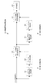
図1において、本実施形態に係る映像信号処理回路10は、信号ソース(図示せず)と表示装置20との間に設けられ、当該信号ソースから与えられる入力映像信号を処理して表示装置20に供給する。一般的にABL回路と呼称される映像信号処理回路10は、好ましくは、2つの制御系、即ち、第1の制御系30と第2の制御系40との組合せから成る構成となっている。そして、第2の制御系40は、第1の制御系30の後段に設けられる。 In FIG. 1, a video signal processing circuit 10 according to the present embodiment is provided between a signal source (not shown) and a display device 20, and processes an input video signal given from the signal source to display the display device 20. To supply. The video signal processing circuit 10 that is generally called an ABL circuit is preferably composed of a combination of two control systems, that is, a first control system 30 and a second control system 40. The second control system 40 is provided at the subsequent stage of the first control system 30.
第1の制御系30は、フレーム平均電流算出部31、フレームゲイン算出部32、及び、フレーム映像信号制御部33を有し、1フレーム(1画面)相当の時間の周期で輝度積算値を算出し、この算出した輝度積算値に基づいて映像信号を制御する。この第1の制御系30は、1フレーム相当の時間の周期で映像信号制御(輝度制御)を行う周知のABL回路に相当する。
The first control system 30 includes a frame average
第1の制御系30において、フレーム平均電流算出部31は、フレーム毎に各フレームの平均電流を算出する。このフレーム平均電流は、1フレームの輝度積算値に相当する。すなわち、フレーム平均電流算出部31では、1フレーム相当の時間の周期で輝度積算値に相当するフレーム平均電流の算出が行われる。
In the first control system 30, the frame average
フレームゲイン算出部32は、フレーム平均電流算出部31が算出したフレーム平均電流に基づいて、制御目標値(フレーム制御目標値)を基準として当該フレームの映像信号に対するゲイン(以下、「フレームゲイン」と記述する)を算出する。フレーム映像信号制御部33は、フレームゲイン算出部32が算出したフレームゲインに基づいて、次フレームの映像信号を制御する。
Based on the frame average current calculated by the frame average
第2の制御系40は、ライン平均積算電流算出部41、ラインゲイン算出部42、及び、ライン映像信号制御部43を有し、例えば1ライン(1画素行)相当の時間の周期で輝度積算値を算出し、この算出した輝度積算値に基づいて映像信号の振幅を制御する。具体的には、輝度積算値が後述する制御目標値よりも大きい(制御目標値を超える)ときに映像信号の振幅が小さくなるように制御する。この第2の制御系40は、本開示の特徴とする部分である。
The second control system 40 includes a line average integrated
ライン平均積算電流算出部41、ラインゲイン算出部42、及び、ライン振幅制御部43の個々の構成について以下に具体的に説明する。
The individual configurations of the line average integrated
(ライン平均積算電流算出部)
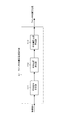
図2は、ライン平均積算電流算出部41の構成の具体例を示すブロック図である。図2に示すように、ライン平均積算電流算出部41は、平均信号算出部411、平均電流算出部412、及び、平均積算電流算出部413を有し、ライン周期(水平走査周期)で回路動作を実行する。
(Line average integrated current calculation part)
FIG. 2 is a block diagram illustrating a specific example of the configuration of the line average integrated
ライン平均積算電流算出部41において、平均信号算出部411は、フレーム映像信号制御部33を経た映像信号に基づいて、ライン毎に平均信号レベルを算出する。平均電流算出部412は、平均信号算出部411が算出した平均信号レベルに基づいて、当該平均信号レベルに対応する平均電流をライン毎に算出する。
In the line average integrated
平均積算電流算出部413は、平均電流算出部412が算出したライン毎の平均電流を現ラインまで積算し、ライン平均積算電流として次段のラインゲイン算出部42に供給する。このライン平均積算電流は、各ラインまでの輝度積算値に相当する。すなわち、平均積算電流算出部413では、1フレーム相当の時間よりも短い周期で輝度積算値に相当するライン平均積算電流の算出が行われる。
The average integrated
(ラインゲイン算出部)
図3は、ラインゲイン算出部42の構成の具体例を示すブロック図である。図3に示すように、ラインゲイン算出部42は、電流比較部421及びゲイン算出部422を有し、ライン周期で回路動作を実行する。
(Line gain calculator)
FIG. 3 is a block diagram illustrating a specific example of the configuration of the line
ラインゲイン算出部42において、電流比較部421は、前段のライン平均積算電流算出部41が算出したライン平均積算電流を、予め定められた制御目標値(ライン制御目標値)と比較する。ここで、第2の制御系40のライン制御目標値は、第1の制御系30のフレーム制御目標値よりも高い値に設定されている(その理由については後述する)。そして、電流比較部421は、ライン平均積算電流が制御目標値以下であるか、制御目標値を超えるかの比較結果を次段のゲイン算出部422に与える。
In the line
ラインゲイン算出部422は、電流比較部421の比較結果を基に、例えば、ライン平均積算電流が制御目標値以下のときはゲイン“1”を、ライン平均積算電流が制御目標値を超えるときはゲイン“0”をラインゲインとして次段のライン映像信号制御部43に供給する。
Based on the comparison result of the
(ライン映像信号制御部)
図4は、ライン映像信号制御部43の構成の具体例を示すブロック図である。図4に示すように、ライン映像信号制御部43は、乗算器431から成り、ライン周期で回路動作を実行する。乗算器431は、フレーム映像信号制御部33を経た映像信号を入力とし、当該入力映像信号に対してラインゲイン算出部42から与えられるラインゲインを乗算することで、映像信号を制御する。
(Line video signal controller)
FIG. 4 is a block diagram illustrating a specific example of the configuration of the line video
このライン映像信号制御部43、即ち、乗算器431における、映像信号の制御によって輝度の制御が行われる。乗算器431から出力される映像信号(出力映像信号)は、表示装置20に供給される。
The line video
[1−2.回路動作]
続いて、上記構成の本実施形態に係る映像信号処理回路10の回路動作について説明する。
[1-2. Circuit operation]
Subsequently, the circuit operation of the video signal processing circuit 10 according to the present embodiment having the above-described configuration will be described.
(第1の制御系)
信号ソース(図示せず)から供給される映像信号は、先ず、第1の制御系30に入力される。第1の制御系30内に入力された映像信号の流れは2つに分岐され、その1つはそのままフレーム映像信号制御部33へ送られ、もう1つはフレーム平均電流算出部31へ送られる。
(First control system)
A video signal supplied from a signal source (not shown) is first input to the first control system 30. The flow of the video signal input into the first control system 30 is branched into two, one of which is sent to the frame video
フレーム映像信号制御部33へ送られた映像信号は、当該フレーム映像信号制御部33において、フレームゲイン算出部32で算出されたフレームゲインに基づく制御を受けた後、次段の第2の制御系40に入力される。一方、フレーム平均電流算出部31へ送られた映像信号は、1フレーム分の映像信号が終わるまでフレーム平均電流を算出するために使用される。
The video signal sent to the frame video
フレーム平均電流算出部31では、1フレーム分の映像信号が終わった段階で当該1フレーム分の平均電流、即ち、1フレーム分の映像信号の輝度積算値に相当するフレーム平均電流が決定される。この決定されたフレーム平均電流は、フレームゲイン算出部32に送られる。フレームゲイン算出部32では、フレーム平均電流算出部31から送られたフレーム平均電流に基づいてフレーム制御目標値を制御基準としてフレームゲインが決定される。この決定されたフレームゲインは、フレーム映像信号制御部33へ送られる。
The frame average
上述したことから明らかなように、第1の制御系30においては、ある1フレームについて輝度積算値に相当するフレーム平均電流が算出され、当該フレーム平均電流に基づいてフレームゲインが決定され、当該フレームゲインが次フレームの映像信号の制御、即ち、輝度制御に反映される。 As is clear from the above, in the first control system 30, a frame average current corresponding to the luminance integrated value is calculated for a certain frame, a frame gain is determined based on the frame average current, and the frame The gain is reflected in the control of the video signal of the next frame, that is, the luminance control.
従って、ある1フレーム内において、フレーム平均電流がフレーム制御目標値を超えたとしても、当該フレームの映像信号に対して輝度制御が行われることはなく、次のフレームの映像信号に対して輝度制御が行われることになる。すなわち、フレーム平均電流の算出結果が輝度制御に反映されるのに必ず1フレーム相当の時間の遅延が生じるため、1フレームの期間は、映像信号の輝度制御、即ち、消費電流(消費電力)低減のための制御が行えないことになる。 Therefore, even if the frame average current exceeds the frame control target value within one frame, the luminance control is not performed on the video signal of the frame, and the luminance control is performed on the video signal of the next frame. Will be done. In other words, since the calculation result of the frame average current is reflected in the luminance control, a time delay corresponding to one frame always occurs. Therefore, during the period of one frame, the luminance control of the video signal, that is, the consumption current (power consumption) is reduced. The control for cannot be performed.
(第2の制御系)
第1の制御系30で制御された映像信号は、第2の制御系40に入力される。第2の制御系40内に入力された映像信号の流れは2つに分岐され、その1つはそのままライン映像信号制御部43へ送られ、もう1つはライン平均積算電流算出部41へ送られる。
(Second control system)
The video signal controlled by the first control system 30 is input to the second control system 40. The flow of the video signal input into the second control system 40 is branched into two, one of which is sent as it is to the line video
ライン映像信号制御部43へ送られた映像信号は、当該ライン映像信号制御部43において、ラインゲイン算出部42で算出されたラインゲインに基づく制御を受けた後、後段の表示装置20のデータドライバ(図示せず)に出力される。ここでは、ライン映像信号制御部43で制御された映像信号を直接表示装置20に供給する構成を採っているが、所望の信号処理を行う信号処理回路を経由して表示装置20に供給する構成を採るようにしてもよい。
The video signal sent to the line video
一方、ライン平均積算電流算出部41へ送られた映像信号は、1ライン分の映像信号が終わるまでライン平均積算電流を算出するために使用される。ライン平均積算電流算出部41では、1ライン分の映像信号が終わった段階で現ラインまでの積算電流、即ち、現ラインまでの輝度積算値に相当するライン平均積算電流が算出され、ラインゲイン算出部42に送られる。
On the other hand, the video signal sent to the line average integrated
ラインゲイン算出部42では、ライン平均積算電流算出部41から送られたライン平均積算電流に基づいてライン制御目標値を制御基準としてラインゲインが決定される。具体的には、例えば、ライン平均積算電流が制御目標値以下のときはラインゲインを“1”とし、ライン平均積算電流が制御目標値を超えるときはラインゲインを“0”とする。このようにして決定されたラインゲインは、ライン映像信号制御部43へ送られる。
In the line
先述したように、第1の制御部30では、1フレームが終了するまで輝度制御を行うことができない。これに対して、第2の制御系40においては、ライン単位で輝度積算値に相当するライン平均積算電流が算出され、当該ライン平均積算電流に基づいてラインゲインが決定され、当該ラインゲインが次ライン以降の映像信号の制御、即ち、輝度制御に反映される。これにより、1フレームの期間を待たなくても、即ち、1フレーム相当の時間よりも短い単位で輝度制御を行うことができることになる。 As described above, the first control unit 30 cannot perform luminance control until one frame is completed. On the other hand, in the second control system 40, a line average integrated current corresponding to the luminance integrated value is calculated for each line, a line gain is determined based on the line average integrated current, and the line gain is This is reflected in video signal control after the line, that is, luminance control. As a result, the luminance control can be performed without waiting for the period of one frame, that is, in a unit shorter than the time corresponding to one frame.
ここで、映像信号の制御、即ち、輝度制御を行うことにより、表示装置20の各画素の電気光学素子に流れる電流を抑えることができるため、表示装置20の消費電流(消費電力)を低減できる。すなわち、映像信号の輝度を制御するということは、表示装置20の消費電流を制御することである。 Here, by controlling the video signal, that is, brightness control, the current flowing through the electro-optic element of each pixel of the display device 20 can be suppressed, so that the current consumption (power consumption) of the display device 20 can be reduced. . In other words, controlling the luminance of the video signal means controlling the current consumption of the display device 20.
(具体例)
ここで、一具体例として、入力映像信号の平均信号レベルが相対的に低い状態から高い状態へ遷移し、消費電流の制御、即ち、映像信号の制御が非動作状態から動作状態へ移行する場合を考える。
(Concrete example)
Here, as a specific example, when the average signal level of the input video signal transitions from a relatively low state to a high state, current consumption control, that is, video signal control transitions from the non-operating state to the operating state. think of.
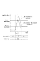
映像信号の制御が非動作状態から動作状態へ移行した瞬間のフレームが開始した時点では、第1の制御系30のフレームゲインとして平均信号レベルが低い状態の値が設定されているため、フレーム映像信号制御部33では当該値のフレームゲインにて制御が行われる。具体的には、図5に示すように、制御が非動作状態から動作状態へ移行する前のフレームでのフレームゲインが例えば1.0の場合には、現フレームのフレームゲインも1.0のままである。
Since the value of the state where the average signal level is low is set as the frame gain of the first control system 30 at the time when the frame at the moment when the control of the video signal shifts from the non-operating state to the operating state is started, the frame video The
すなわち、フレーム映像信号制御部33からは、制御が非動作状態から動作状態へ移行する前と同じ映像信号が出力される。従って、従来技術に相当する第1の制御系30のみによる制御では、入力映像信号の平均信号レベルが相対的に低い状態から高い状態へ移行したにも拘わらず、制御が行われていない映像信号が表示装置20へ入力される。これにより、制御が非動作状態から動作状態へ移行したときの1フレームの前後最大2フレームの期間において過電流が発生し、当該12フレームの期間が終了するまで消費電流の制御が行えないことになる。
That is, the same video signal as before the control shifts from the non-operating state to the operating state is output from the frame video
これに対し、本実施形態では、第1の制御系30の後段に第2の制御系40を配し、当該第2の制御系40において、1ライン毎に映像信号の制御を行うようにしている。従って、制御が非動作状態から動作状態へ移行した瞬間のフレームにおいて、ライン平均積算電流がライン制御目標値を超えると、図5に示すように、次ラインから最終ラインまでラインゲインが例えば0.0に設定される。ラインゲインが0.0に設定されることで、映像信号の信号レベルが0になるため、次ラインから最終ラインまでの期間に亘って黒(黒帯)表示となる。 On the other hand, in the present embodiment, a second control system 40 is arranged after the first control system 30, and the video signal is controlled for each line in the second control system 40. Yes. Therefore, when the line average integrated current exceeds the line control target value in the frame at the moment when the control shifts from the non-operating state to the operating state, as shown in FIG. Set to zero. By setting the line gain to 0.0, the signal level of the video signal becomes 0, so that black (black band) is displayed over the period from the next line to the last line.
これにより、1フレームの期間が終了するのを待たなくても、ライン単位で映像信号の輝度制御を行うことができるため、最大2フレーム間の過電流を抑えることができる。ここでは、ライン平均積算電流がライン制御目標値を超えたとき黒表示を行うとしたが、これは一例に過ぎず、例えばグレー表示を行うようにしてもよい。 Accordingly, since it is possible to control the luminance of the video signal in units of lines without waiting for the end of the period of one frame, an overcurrent between a maximum of two frames can be suppressed. Here, black display is performed when the line average integrated current exceeds the line control target value. However, this is only an example, and gray display may be performed, for example.
入力映像信号の平均信号レベルが相対的に低い状態から高い状態へ移行したときのフレームが終わり、次のフレームが開始した時点では、図5に示すように、フレームゲインとして平均信号レベルが高い状態での値、即ち、前フレームで算出された値(例えば、0.4)が設定される。従って、フレーム映像信号制御部33では当該値のフレームゲインにて制御が行われる。
When the frame when the average signal level of the input video signal transitions from a relatively low state to a high state ends and the next frame starts, the average signal level is high as the frame gain as shown in FIG. In other words, the value calculated in the previous frame (for example, 0.4) is set. Accordingly, the frame video
すなわち、フレーム映像信号制御部33からは、前フレームで算出された値のフレームゲインに対応した小さい映像信号が出力される。これにより、後段の第2の制御系40では、入力される映像信号の信号が小さくなっており、また、制御目標値が第1の制御系30のそれよりも高く設定されているため、以降、ライン単位での制御は行われない、即ち、ライン単位での制御が非動作状態になる。
That is, a small video signal corresponding to the frame gain of the value calculated in the previous frame is output from the frame video
尚、図5は、ある時間における瞬時的なパネル消費電流を表している。表示パネルが線順次駆動の場合で、表示画像がラスター画像(全面で均一な画像)の場合、図5に示すような挙動になる。放送信号のような自然画においては、図5のカーブは非線形の複雑な挙動を示す。 FIG. 5 shows the instantaneous panel current consumption at a certain time. When the display panel is line-sequentially driven and the display image is a raster image (a uniform image on the entire surface), the behavior is as shown in FIG. In a natural picture such as a broadcast signal, the curve in FIG. 5 shows a nonlinear complex behavior.
(作用、効果)
上述したように、本実施形態に係る映像信号処理回路10によれば、入力映像信号の平均信号レベルが相対的に低い状態から高い状態へ移行した瞬間のフレームでは、第2の制御系40による制御が動作する。そして、当該フレーム以外のフレームでは、第2の制御系40による制御が動作せず、第1の制御系30による制御が動作する。
(Function, effect)
As described above, according to the video signal processing circuit 10 according to the present embodiment, the second control system 40 uses the frame at the moment when the average signal level of the input video signal shifts from a relatively low state to a high state. Control works. Then, in the frames other than the frame, the control by the second control system 40 does not operate, and the control by the first control system 30 operates.
これにより、1フレーム相当の時間待たなくても、映像信号の輝度制御を行うことができるため、従来方式と同様の電流制御を行いつつ、1フレーム相当の遅延の無い消費電流(電力)の制御の実現が可能になり、最大2フレーム間の過電流を防止することができる。そして、表示装置20を搭載する電子機器によっては、1フレーム間の消費電力の上限が定められているため、1フレーム間の消費電力を制御できることで、1フレーム間の消費電力の上限が定められている電子機器、特に、携帯型の電子機器への適用に際して好適なものとなる。 As a result, the luminance control of the video signal can be performed without waiting for a time corresponding to one frame. Therefore, the current control similar to the conventional method is performed, and current consumption (power) control without delay corresponding to one frame is performed. And overcurrent between a maximum of two frames can be prevented. And since the upper limit of the power consumption between 1 frames is defined depending on the electronic device which mounts the display apparatus 20, the upper limit of the power consumption between 1 frames is determined by controlling the power consumption between 1 frames. The present invention is suitable for application to electronic devices, particularly portable electronic devices.
因みに、フレームメモリを用いる手法を採ることによっても、1フレーム相当の時間待たなくても、映像信号の輝度制御を可能にすることができる。しかし、フレームメモリを用いるとコストアップになる。これに対して、本実施形態に係る映像信号処理回路10の構成、即ち、第1の制御系30と第2の制御系40とを併用する構成を採ることで、高価なフレームメモリを用いる必要がないため、低コストにて所期の目的を達成することができる利点がある。 Incidentally, it is possible to control the luminance of the video signal by adopting a method using a frame memory and without waiting for a time corresponding to one frame. However, using a frame memory increases the cost. On the other hand, it is necessary to use an expensive frame memory by adopting the configuration of the video signal processing circuit 10 according to the present embodiment, that is, the configuration using the first control system 30 and the second control system 40 together. Therefore, there is an advantage that the intended purpose can be achieved at low cost.
また、フレーム単位で制御を行う第1の制御系30と、ライン単位で制御を行う第2の制御系40との配置に関しては、第1の制御系30が前段で、第2の制御系40が後段となる配置関係が好ましい。何故なら、第2の制御系40が前段だと、当該第2の制御系40による制御が頻繁に行われ、その都度画面に黒帯が表示されることによって画質を悪化させることになる。 Further, regarding the arrangement of the first control system 30 that performs control in units of frames and the second control system 40 that performs control in units of lines, the first control system 30 is the preceding stage, and the second control system 40. The arrangement relationship in which the latter is the latter is preferable. This is because if the second control system 40 is in the previous stage, the control by the second control system 40 is frequently performed, and a black belt is displayed on the screen each time, thereby deteriorating the image quality.
これに対して、第2の制御系40が後段だと、前段の第1の制御系30で制御が行われた映像信号に対して制御を行うことになるため、第2の制御系40を前段に配置する場合のような不具合は発生しない。すなわち、第1の制御系30による振幅制御が行われないフレームに対して、第2の制御系40による制御が行われることになるため、黒帯が発生するとしても当該フレームだけで澄むことになる。 On the other hand, if the second control system 40 is in the subsequent stage, the video signal controlled by the first control system 30 in the previous stage is controlled. There is no problem as in the case of the previous stage. That is, since the control by the second control system 40 is performed for a frame for which the amplitude control by the first control system 30 is not performed, even if a black belt is generated, the frame is cleared only by that frame. Become.
因みに、第1の制御系30による制御が行われないフレームに対してだけ第2の制御系40による制御が行われるようにするためには、第2の制御系40の制御目標値を第1の制御系30の制御目標値よりも高い値に設定することが必要となる。 Incidentally, in order to perform the control by the second control system 40 only on the frame that is not controlled by the first control system 30, the control target value of the second control system 40 is set to the first value. It is necessary to set a value higher than the control target value of the control system 30.
<2.変形例>
上記の回路例では、第2の制御系40による制御(輝度制御)を1ライン相当の時間の周期で(即ち、1ライン毎に)行う構成を採る場合を例に挙げたが、当該制御を複数ライン相当の時間の周期で(即ち、複数ライン毎に)行う構成を採ることも可能である。
<2. Modification>
In the above circuit example, the case where the configuration in which the control (luminance control) by the second control system 40 is performed at a period of time corresponding to one line (that is, every line) is taken as an example. It is also possible to adopt a configuration that is performed with a period of time corresponding to a plurality of lines (that is, for each of a plurality of lines).
また、第2の制御系40による制御を、1ライン相当の時間の単位、即ち、1ライン毎あるいは複数ライン毎に行うのではなく、1ドット(1画素)相当の時間の単位、即ち、1ドット毎あるいは複数ドット毎に行うようにしてもよい。但し、1ライン相当の時間の単位で制御を行う方が、水平ブランキング期間においてライン平均積算電流の算出やラインゲインの算出の各処理を行うことができるため、1ドット相当の時間の単位で行う場合に比べて、算出処理の時間を特別に確保する必要が無い点で有利である。 In addition, the control by the second control system 40 is not performed in units of time corresponding to one line, that is, for each line or every plurality of lines, but in units of time corresponding to one dot (one pixel), that is, 1 You may make it carry out for every dot or every several dots. However, when the control is performed in units of time equivalent to one line, each process of calculating the line average integrated current and the line gain can be performed in the horizontal blanking period, and therefore in units of time equivalent to one dot. Compared with the case where it carries out, it is advantageous at the point which does not need to ensure the time of calculation processing specially.
(ドット単位の振幅制御)
図6は、1ドット毎に制御を行う変形例に係る映像信号処理回路の回路構成を示すブロック図であり、図中、図1と同等部位には同一符号を付して示している。
(Amplitude control in dot units)
FIG. 6 is a block diagram showing a circuit configuration of a video signal processing circuit according to a modified example in which control is performed for each dot. In FIG. 6, parts that are the same as those in FIG.
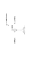
本変形例に係る映像信号処理回路10´は、先述した実施形態に係る映像信号処理回路10と比べて、第2の制御系40´の構成が第2の制御系40の構成と相違している。すなわち、第2の制御系40´は、ライン平均積算電流算出部41、ラインゲイン算出部42、及び、ライン映像信号制御部43に代えて、ドット電流算出部44、ドットゲイン算出部45、及び、ドット映像信号制御部46を用い、例えば1ドット相当の時間の周期で制御を行う構成となっている。
Compared with the video signal processing circuit 10 according to the above-described embodiment, the video signal processing circuit 10 ′ according to this modification is different from the configuration of the second control system 40 in the configuration of the second control system 40 ′. Yes. That is, the second control system 40 ′ replaces the line average integrated
第2の制御系40´において、ドット電流算出部44は、1ドット相当の時間の周期で制御を行う場合は、1画素の輝度に相当するドット電流を検出し、複数ドット相当の時間の周期で制御を行う場合は、複数画素の輝度積算値に相当するドット平均電流を検出することになる。このドット単位で制御を行う第2の制御系40´によれば、ライン単位で制御を行う場合に比べて、より短い周期で消費電流の制御を行うことができる。
In the second control system 40 ′, the dot
(表示装置)
以上では、本開示の実施形態またはその変形例に係る映像信号処理回路10,10´を表示装置20の外部回路として位置付けているが、表示装置20を表示パネルとし、当該表示パネル20及び映像信号処理回路10,10´を表示装置(本開示による表示装置)としてもよい。
(Display device)
In the above, the video signal processing circuits 10 and 10 ′ according to the embodiment of the present disclosure or the modification thereof are positioned as external circuits of the display device 20. However, the display device 20 is a display panel, and the display panel 20 and the video signal are displayed. The processing circuits 10 and 10 ′ may be a display device (a display device according to the present disclosure).
表示装置(パネル)20としては、広く知られている液晶表示装置(LCD)、プラズマ表示装置(PDP)の他、画素の発光素子として電流駆動型の電気光学素子、例えば、有機エレクトロルミネッセンス(EL)素子を用いた有機EL表示装置等を挙げることができる。電流駆動型の電気光学素子は、デバイスに流れる電流値に応じて発光輝度が変化する発光素子である。この電流駆動型の電気光学素子としては、有機EL素子以外にも、無機EL素子、LED素子、半導体レーザー素子などを挙げることができる。 As the display device (panel) 20, in addition to a widely known liquid crystal display device (LCD) and plasma display device (PDP), a current-driven electro-optical element, for example, organic electroluminescence (EL) is used as a light emitting element of a pixel. ) An organic EL display device using an element can be used. A current-driven electro-optical element is a light-emitting element whose light emission luminance changes according to the value of a current flowing through the device. Examples of the current-driven electro-optical element include an inorganic EL element, an LED element, and a semiconductor laser element in addition to the organic EL element.
<3.電子機器>
以上説明した本開示の実施形態またはその変形例に係る映像信号処理回路を備える表示装置(本開示による表示装置)は、電子機器に入力された映像信号、若しくは、電子機器内で生成した映像信号を、画像若しくは映像として表示するあらゆる分野の電子機器の表示部に適用できる。具体的には、本開示による表示装置は、例えば、デジタルカメラ、ノート型パーソナルコンピュータ、携帯電話等の携帯端末装置、ビデオカメラなどの表示部として用いることが可能である。
<3. Electronic equipment>
A display device (a display device according to the present disclosure) including the video signal processing circuit according to the embodiment of the present disclosure described above or a modification thereof is a video signal input to an electronic device or a video signal generated in the electronic device. Can be applied to display portions of electronic devices in various fields that display images or videos. Specifically, the display device according to the present disclosure can be used as a display unit of, for example, a digital camera, a notebook personal computer, a mobile terminal device such as a mobile phone, and a video camera.
先述した実施形態またはその変形例の説明から明らかなように、本開示による映像信号処理回路によれば、最大2フレーム間の消費電力を制御できる。従って、本開示による映像信号処理回路を備える表示装置は、特に、1フレーム間の消費電力の上限が定められている電子機器において、その表示部として用いることで、表示装置の消費電力を一定以下に制限することができるため、電子機器の低消費電力化に寄与できる。 As is apparent from the description of the above-described embodiment or its modification, the video signal processing circuit according to the present disclosure can control power consumption between a maximum of two frames. Therefore, a display device including the video signal processing circuit according to the present disclosure is used as a display unit in an electronic device in which an upper limit of power consumption between one frame is determined, thereby reducing the power consumption of the display device below a certain level. Therefore, it is possible to contribute to lower power consumption of electronic devices.
以下に、本開示が適用される電子機器の具体例について説明する。 Specific examples of electronic devices to which the present disclosure is applied will be described below.
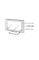
図7は、本開示が適用されるテレビジョンセットの外観を示す斜視図である。本適用例に係るテレビジョンセットは、フロントパネル102やフィルターガラス103等から構成される映像表示画面部101を含み、その映像表示画面部101として本開示による表示装置を用いることにより作製される。 FIG. 7 is a perspective view illustrating an appearance of a television set to which the present disclosure is applied. The television set according to this application example includes a video display screen unit 101 including a front panel 102, a filter glass 103, and the like, and is manufactured by using the display device according to the present disclosure as the video display screen unit 101.
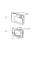
図8は、本開示が適用されるデジタルカメラの外観を示す斜視図であり、(A)は表側から見た斜視図、(B)は裏側から見た斜視図である。本適用例に係るデジタルカメラは、フラッシュ用の発光部111、表示部112、メニュースイッチ113、シャッターボタン114等を含み、その表示部112として本開示による表示装置を用いることにより作製される。 8A and 8B are perspective views illustrating an appearance of a digital camera to which the present disclosure is applied, in which FIG. 8A is a perspective view seen from the front side, and FIG. 8B is a perspective view seen from the back side. The digital camera according to this application example includes a light emitting unit 111 for flash, a display unit 112, a menu switch 113, a shutter button 114, and the like, and is manufactured by using the display device according to the present disclosure as the display unit 112.
図9は、本開示が適用されるノート型パーソナルコンピュータの外観を示す斜視図である。本適用例に係るノート型パーソナルコンピュータは、本体121に、文字等を入力するとき操作されるキーボード122、画像を表示する表示部123等を含み、その表示部123として本開示による表示装置を用いることにより作製される。 FIG. 9 is a perspective view illustrating an appearance of a notebook personal computer to which the present disclosure is applied. The notebook personal computer according to this application example includes a main body 121 including a keyboard 122 operated when inputting characters and the like, a display unit 123 that displays an image, and the like, and the display device according to the present disclosure is used as the display unit 123. It is produced by this.
図10は、本開示が適用されるビデオカメラの外観を示す斜視図である。本適用例に係るビデオカメラは、本体部131、前方を向いた側面に被写体撮影用のレンズ132、撮影時のスタート/ストップスイッチ133、表示部134等を含み、その表示部134として本開示による表示装置を用いることにより作製される。 FIG. 10 is a perspective view illustrating an appearance of a video camera to which the present disclosure is applied. The video camera according to this application example includes a main body 131, a lens 132 for shooting an object on a side facing forward, a start / stop switch 133 at the time of shooting, a display unit 134, and the like. It is manufactured by using a display device.
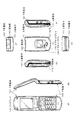
図11は、本開示が適用される携帯端末装置、例えば携帯電話機を示す外観図であり、(A)は開いた状態での正面図、(B)はその側面図、(C)は閉じた状態での正面図、(D)は左側面図、(E)は右側面図、(F)は上面図、(G)は下面図である。本適用例に係る携帯電話機は、上側筐体141、下側筐体142、連結部(ここではヒンジ部)143、ディスプレイ144、サブディスプレイ145、ピクチャーライト146、カメラ147等を含んでいる。そして、ディスプレイ144やサブディスプレイ145として本開示による表示装置を用いることにより、本適用例に係る携帯電話機が作製される。 FIG. 11 is an external view showing a mobile terminal device to which the present disclosure is applied, for example, a mobile phone, in which (A) is a front view in an opened state, (B) is a side view thereof, and (C) is closed. (D) is a left side view, (E) is a right side view, (F) is a top view, and (G) is a bottom view. A cellular phone according to this application example includes an upper casing 141, a lower casing 142, a connecting portion (here, a hinge portion) 143, a display 144, a sub-display 145, a picture light 146, a camera 147, and the like. Then, by using the display device according to the present disclosure as the display 144 or the sub display 145, the mobile phone according to the application example is manufactured.
<4.本開示の構成>
(1)入力される映像信号に基づいて輝度積算値を算出し、この算出した輝度積算値に基づいて前記映像信号の輝度制御を行う制御部を有し、
前記制御部は、1フレーム相当の時間よりも短い周期で前記輝度積算値の算出を行う
映像信号処理回路。
(2)前記制御部は、前記輝度積算値が制御目標値よりも大きいときに前記映像信号の振幅が小さくなるように制御する
前記(1)に記載の映像信号処理回路。
(3)前記1フレーム相当の時間よりも短い周期は、1ライン相当の時間の単位である
前記(1)または前記(2)に記載の映像信号処理回路。
(4)前記1フレーム相当の時間よりも短い周期は、1ライン相当の時間である
前記(3)に記載の映像信号処理回路。
(5)前記1フレーム相当の時間よりも短い周期は、複数ライン相当の時間である
前記(3)に記載の映像信号処理回路。
(6)前記1フレーム相当の時間よりも短い周期は、1ドット相当の時間の単位である
前記(1)または前記(2)に記載の映像信号処理回路。
(7)1フレーム相当の時間の周期で輝度積算値を算出し、この算出した輝度積算値に基づいて映像信号を制御する第1の制御系と、
1フレーム相当の時間よりも短い周期で輝度積算値を算出し、この算出した輝度積算値に基づいて映像信号を制御する第2の制御系と
を備える映像信号処理回路。
(8)前記第1の制御系及び前記第2の制御系は、前記輝度積算値が制御目標値よりも大きいときに前記映像信号が小さくなるように制御する
前記(7)に記載の映像信号処理回路。
(9)前記第2の制御系は、1ライン相当の時間の単位で前記輝度積算値の算出を行う
前記(7)または前記(8)に記載の映像信号処理回路。
(10)前記第2の制御系は、1ライン相当の時間の周期で前記輝度積算値の算出を行う
前記(9)に記載の映像信号処理回路。
(11)前記第2の制御系は、複数ライン相当の時間の周期で前記輝度積算値の算出を行う
前記(9)に記載の映像信号処理回路。
(12)前記第2の制御系は、1ドット相当の時間の単位で前記輝度積算値の算出を行う
前記(7)に記載の映像信号処理回路。
(13)前記第2の制御系は、前記第1の制御系の後段に設けられている
前記(7)から前記(12)のいずれかに記載の映像信号処理回路。
(14)前記第2の制御系の制御目標値は、前記第1の制御系の制御目標値よりも高い値に設定されている
前記(13)に記載の映像信号処理回路。
(15)入力される映像信号に基づいて輝度積算値を算出し、この算出した輝度積算値に基づいて前記映像信号の輝度制御を行うに当たって、
1フレーム相当の時間よりも短い周期で前記輝度積算値の算出を行う
映像信号処理方法。
(16)入力される映像信号に基づいて輝度積算値を1フレーム相当の時間よりも短い周期で算出し、この算出した輝度積算値に基づいて前記映像信号の輝度制御を行う制御部
を備える表示装置。
(17)入力される映像信号に基づいて輝度積算値を1フレーム相当の時間よりも短い周期で算出し、この算出した輝度積算値に基づいて前記映像信号の輝度制御を行う制御部
を備える表示装置を有する電子機器。
<4. Configuration of the present disclosure>
(1) a control unit that calculates a luminance integrated value based on the input video signal and performs luminance control of the video signal based on the calculated luminance integrated value;
The video signal processing circuit, wherein the control unit calculates the luminance integrated value in a cycle shorter than a time corresponding to one frame.
(2) The video signal processing circuit according to (1), wherein the control unit controls the amplitude of the video signal to be small when the luminance integrated value is larger than a control target value.
(3) The video signal processing circuit according to (1) or (2), wherein the period shorter than the time corresponding to one frame is a unit of time corresponding to one line.
(4) The video signal processing circuit according to (3), wherein the period shorter than the time corresponding to one frame is a time corresponding to one line.
(5) The video signal processing circuit according to (3), wherein the cycle shorter than the time corresponding to one frame is a time corresponding to a plurality of lines.
(6) The video signal processing circuit according to (1) or (2), wherein the period shorter than the time corresponding to one frame is a unit of time corresponding to one dot.
(7) a first control system that calculates a luminance integrated value at a period of time corresponding to one frame and controls a video signal based on the calculated luminance integrated value;
A video signal processing circuit comprising: a second control system that calculates a luminance integrated value in a cycle shorter than a time corresponding to one frame and controls the video signal based on the calculated luminance integrated value.
(8) The video signal according to (7), wherein the first control system and the second control system control the video signal to be small when the luminance integrated value is larger than a control target value. Processing circuit.
(9) The video signal processing circuit according to (7) or (8), wherein the second control system calculates the luminance integrated value in a unit of time corresponding to one line.
(10) The video signal processing circuit according to (9), wherein the second control system calculates the luminance integrated value at a period of time corresponding to one line.
(11) The video signal processing circuit according to (9), wherein the second control system calculates the luminance integrated value at a period of time corresponding to a plurality of lines.
(12) The video signal processing circuit according to (7), wherein the second control system calculates the luminance integrated value in a unit of time corresponding to one dot.
(13) The video signal processing circuit according to any one of (7) to (12), wherein the second control system is provided at a subsequent stage of the first control system.
(14) The video signal processing circuit according to (13), wherein the control target value of the second control system is set to a value higher than the control target value of the first control system.
(15) A luminance integrated value is calculated based on the input video signal, and the luminance control of the video signal is performed based on the calculated luminance integrated value.
A video signal processing method for calculating the luminance integrated value in a cycle shorter than a time corresponding to one frame.
(16) A display including a control unit that calculates a luminance integrated value in a cycle shorter than a time corresponding to one frame based on an input video signal and performs luminance control of the video signal based on the calculated luminance integrated value. apparatus.
(17) A display including a control unit that calculates a luminance integrated value in a cycle shorter than a time corresponding to one frame based on an input video signal and performs luminance control of the video signal based on the calculated luminance integrated value. An electronic device having a device.
10,10´・・・映像信号処理回路、20・・・表示装置、30・・・第1の制御系、31・・・フレーム平均電流算出部、32・・・フレームゲイン算出部、33・・・フレーム映像信号制御部、40,40´・・・第2の制御系、41・・・ライン平均積算電流算出部、42・・・ラインゲイン算出部、43・・・ライン映像信号制御部 10, 10 '... video signal processing circuit, 20 ... display device, 30 ... first control system, 31 ... frame average current calculator, 32 ... frame gain calculator, 33 ..Frame video signal control unit, 40, 40 '... second control system, 41 ... line average integrated current calculation unit, 42 ... line gain calculation unit, 43 ... line video signal control unit
Claims (17)
前記制御部は、1フレーム相当の時間よりも短い周期で前記輝度積算値の算出を行う
映像信号処理回路。 A control unit that calculates a luminance integrated value based on the input video signal and performs luminance control of the video signal based on the calculated luminance integrated value;
The video signal processing circuit, wherein the control unit calculates the luminance integrated value in a cycle shorter than a time corresponding to one frame.
請求項1に記載の映像信号処理回路。 The video signal processing circuit according to claim 1, wherein the control unit controls the amplitude of the video signal to be small when the luminance integrated value is larger than a control target value.
請求項1に記載の映像信号処理回路。 The video signal processing circuit according to claim 1, wherein the period shorter than the time corresponding to one frame is a unit of time corresponding to one line.
請求項3に記載の映像信号処理回路。 The video signal processing circuit according to claim 3, wherein the period shorter than the time corresponding to one frame is a time corresponding to one line.
請求項3に記載の映像信号処理回路。 The video signal processing circuit according to claim 3, wherein the period shorter than the time corresponding to one frame is a time corresponding to a plurality of lines.
請求項1に記載の映像信号処理回路。 The video signal processing circuit according to claim 1, wherein the period shorter than the time corresponding to one frame is a unit of time corresponding to one dot.
1フレーム相当の時間よりも短い周期で輝度積算値を算出し、この算出した輝度積算値に基づいて映像信号を制御する第2の制御系
を備える映像信号処理回路。 A first control system that calculates a luminance integrated value at a period of time corresponding to one frame and controls a video signal based on the calculated luminance integrated value;
A video signal processing circuit comprising: a second control system that calculates a luminance integrated value at a cycle shorter than a time corresponding to one frame and controls a video signal based on the calculated luminance integrated value.
請求項7に記載の映像信号処理回路。 The video signal processing circuit according to claim 7, wherein the first control system and the second control system control the video signal to be small when the luminance integrated value is larger than a control target value.
請求項7に記載の映像信号処理回路。 The video signal processing circuit according to claim 7, wherein the second control system calculates the luminance integrated value in a unit of time corresponding to one line.
請求項9に記載の映像信号処理回路。 The video signal processing circuit according to claim 9, wherein the second control system calculates the luminance integrated value at a period of time corresponding to one line.
請求項9に記載の映像信号処理回路。 The video signal processing circuit according to claim 9, wherein the second control system calculates the luminance integrated value at a period of time corresponding to a plurality of lines.
請求項7に記載の映像信号処理回路。 The video signal processing circuit according to claim 7, wherein the second control system calculates the luminance integrated value in a unit of time corresponding to one dot.
請求項7に記載の映像信号処理回路。 The video signal processing circuit according to claim 7, wherein the second control system is provided in a subsequent stage of the first control system.
請求項13に記載の映像信号処理回路。 The video signal processing circuit according to claim 13, wherein a control target value of the second control system is set to a value higher than a control target value of the first control system.
1フレーム相当の時間よりも短い周期で前記輝度積算値の算出を行う
映像信号処理方法。 In calculating the luminance integrated value based on the input video signal, and performing the luminance control of the video signal based on the calculated luminance integrated value,
A video signal processing method for calculating the luminance integrated value in a cycle shorter than a time corresponding to one frame.
を備える表示装置。 A display device comprising: a control unit that calculates a luminance integrated value based on an input video signal in a cycle shorter than a time corresponding to one frame, and performs luminance control of the video signal based on the calculated luminance integrated value.
を備える表示装置を有する電子機器。 A display device comprising: a control unit that calculates a luminance integrated value based on an input video signal in a cycle shorter than a time corresponding to one frame, and performs luminance control of the video signal based on the calculated luminance integrated value. Electronics.
Priority Applications (3)
| Application Number | Priority Date | Filing Date | Title |
|---|---|---|---|
| JP2011132006A JP2013003238A (en) | 2011-06-14 | 2011-06-14 | Video signal processing circuit, video signal processing method, display device, and electronic apparatus |
| US13/460,177 US8896758B2 (en) | 2011-06-14 | 2012-04-30 | Video signal processing circuit, video signal processing method, display device, and electronic apparatus |
| CN2012101950642A CN102831874A (en) | 2011-06-14 | 2012-06-13 | Video signal processing circuit, video signal processing method, display device, and electronic apparatus |
Applications Claiming Priority (1)
| Application Number | Priority Date | Filing Date | Title |
|---|---|---|---|
| JP2011132006A JP2013003238A (en) | 2011-06-14 | 2011-06-14 | Video signal processing circuit, video signal processing method, display device, and electronic apparatus |
Publications (2)
| Publication Number | Publication Date |
|---|---|
| JP2013003238A true JP2013003238A (en) | 2013-01-07 |
| JP2013003238A5 JP2013003238A5 (en) | 2014-06-19 |
Family
ID=47334973
Family Applications (1)
| Application Number | Title | Priority Date | Filing Date |
|---|---|---|---|
| JP2011132006A Pending JP2013003238A (en) | 2011-06-14 | 2011-06-14 | Video signal processing circuit, video signal processing method, display device, and electronic apparatus |
Country Status (3)
| Country | Link |
|---|---|
| US (1) | US8896758B2 (en) |
| JP (1) | JP2013003238A (en) |
| CN (1) | CN102831874A (en) |
Families Citing this family (5)
| Publication number | Priority date | Publication date | Assignee | Title |
|---|---|---|---|---|
| JP5221780B1 (en) * | 2012-02-03 | 2013-06-26 | シャープ株式会社 | Video display device and television receiver |
| JP6167324B2 (en) * | 2012-07-25 | 2017-07-26 | 株式会社Joled | Display device, image processing device, and image processing method |
| US20140285531A1 (en) * | 2013-03-19 | 2014-09-25 | Ericsson Television Inc. | System, method, and device for adjusting display luminance |
| US10789892B2 (en) * | 2015-03-11 | 2020-09-29 | Facebook Technologies, Llc | Dynamic illumination persistence for organic light emitting diode display device |
| KR20230064719A (en) * | 2021-11-04 | 2023-05-11 | 주식회사 엘엑스세미콘 | Display Device And Apparatus and Method for Driving Display Device |
Citations (8)
| Publication number | Priority date | Publication date | Assignee | Title |
|---|---|---|---|---|
| JP2005070426A (en) * | 2003-08-25 | 2005-03-17 | Seiko Epson Corp | Electrooptical device, method for driving electrooptical device, and electronic equipment |
| JP2005257754A (en) * | 2004-03-09 | 2005-09-22 | Pioneer Electronic Corp | Display apparatus |
| JP2007147731A (en) * | 2005-11-24 | 2007-06-14 | Tohoku Pioneer Corp | Display control apparatus for video signal and display control method |
| JP2007212644A (en) * | 2006-02-08 | 2007-08-23 | Matsushita Electric Ind Co Ltd | Spontaneous light display device |
| JP2007248653A (en) * | 2006-03-14 | 2007-09-27 | Eastman Kodak Co | Driving device of display device or method of driving display device |
| JP2007298693A (en) * | 2006-04-28 | 2007-11-15 | Matsushita Electric Ind Co Ltd | Video display device and semiconductor circuit |
| JP2008026761A (en) * | 2006-07-25 | 2008-02-07 | Sony Corp | Power consumption controller and control method, image processor, self-luminous light emitting display device, electronic equipment, and computer program |
| JP2008026395A (en) * | 2006-07-18 | 2008-02-07 | Sony Corp | Power consumption detection device and method, power consumption controller, image processor, self-luminous light emitting display device, electronic equipment, power consumption control method, and computer program |
Family Cites Families (41)
| Publication number | Priority date | Publication date | Assignee | Title |
|---|---|---|---|---|
| US6836288B1 (en) * | 1999-02-09 | 2004-12-28 | Linvatec Corporation | Automatic exposure control system and method |
| JP3695737B2 (en) * | 1999-07-01 | 2005-09-14 | パイオニア株式会社 | Driving device for plasma display panel |
| CA2322593C (en) * | 1999-10-08 | 2004-02-03 | Matsushita Electric Industrial Co., Ltd. | Method and apparatus for detection and correction of illumination flicker |
| US6771243B2 (en) * | 2001-01-22 | 2004-08-03 | Matsushita Electric Industrial Co., Ltd. | Display device and method for driving the same |
| JP4416959B2 (en) * | 2001-04-26 | 2010-02-17 | 富士通マイクロエレクトロニクス株式会社 | Flicker noise reduction method for XY address type solid-state imaging device |
| US6985141B2 (en) * | 2001-07-10 | 2006-01-10 | Canon Kabushiki Kaisha | Display driving method and display apparatus utilizing the same |
| JP3823314B2 (en) * | 2001-12-18 | 2006-09-20 | ソニー株式会社 | Imaging signal processing apparatus and flicker detection method |
| JP2003255901A (en) | 2001-12-28 | 2003-09-10 | Sanyo Electric Co Ltd | Organic el display luminance control method and luminance control circuit |
| CN101221728A (en) * | 2001-12-28 | 2008-07-16 | 三洋电机株式会社 | Luminance control method and luminance control circuit for organic EL display |
| JP3995505B2 (en) * | 2002-03-25 | 2007-10-24 | 三洋電機株式会社 | Display method and display device |
| JP4794801B2 (en) * | 2002-10-03 | 2011-10-19 | ルネサスエレクトロニクス株式会社 | Display device for portable electronic device |
| US7348957B2 (en) * | 2003-02-14 | 2008-03-25 | Intel Corporation | Real-time dynamic design of liquid crystal display (LCD) panel power management through brightness control |
| JP2004260574A (en) * | 2003-02-26 | 2004-09-16 | Matsushita Electric Ind Co Ltd | Flicker detecting method and detector |
| US7106352B2 (en) * | 2003-03-03 | 2006-09-12 | Sun Microsystems, Inc. | Automatic gain control, brightness compression, and super-intensity samples |
| US7259769B2 (en) * | 2003-09-29 | 2007-08-21 | Intel Corporation | Dynamic backlight and image adjustment using gamma correction |
| JP4341839B2 (en) * | 2003-11-17 | 2009-10-14 | シャープ株式会社 | Image display device, electronic apparatus, liquid crystal television device, liquid crystal monitor device, image display method, display control program, and recording medium |
| US7154468B2 (en) * | 2003-11-25 | 2006-12-26 | Motorola Inc. | Method and apparatus for image optimization in backlit displays |
| KR20050052193A (en) * | 2003-11-29 | 2005-06-02 | 삼성에스디아이 주식회사 | Panel driving device |
| JP3802536B2 (en) * | 2004-02-20 | 2006-07-26 | 沖電気工業株式会社 | Auto gain control circuit |
| JP4403401B2 (en) * | 2004-10-13 | 2010-01-27 | ソニー株式会社 | Information processing apparatus and method, recording medium, and program |
| KR100629586B1 (en) * | 2005-03-31 | 2006-09-27 | 삼성에스디아이 주식회사 | Light emitting display and driving method thereof |
| EP2184733B1 (en) * | 2005-11-07 | 2012-08-22 | Sharp Kabushiki Kaisha | Image displaying apparatus |
| TWI325575B (en) * | 2005-11-24 | 2010-06-01 | Ind Tech Res Inst | Method and structure for automatic adjusting brightness and display apparatus |
| JP2007156045A (en) * | 2005-12-05 | 2007-06-21 | Sony Corp | Spontaneous light emission display device, power consumption detecting device, and program |
| JP4621585B2 (en) * | 2005-12-15 | 2011-01-26 | 株式会社東芝 | Image processing apparatus and image processing method |
| US7728829B2 (en) * | 2006-01-13 | 2010-06-01 | Hewlett-Packard Development Company, L.P. | Display system |
| JP4555785B2 (en) * | 2006-02-10 | 2010-10-06 | シャープ株式会社 | Fixed pattern noise removal device, solid-state imaging device, electronic device, and fixed pattern noise removal program |
| JP4208904B2 (en) * | 2006-07-03 | 2009-01-14 | キヤノン株式会社 | Imaging apparatus, control method therefor, and imaging system |
| JP4353223B2 (en) * | 2006-09-07 | 2009-10-28 | ソニー株式会社 | Image data processing apparatus, image data processing method, and imaging system |
| JP4491646B2 (en) * | 2006-09-08 | 2010-06-30 | 株式会社 日立ディスプレイズ | Display device |
| JP4259567B2 (en) * | 2006-11-02 | 2009-04-30 | セイコーエプソン株式会社 | Projector, projection system, program, and recording medium |
| US20080238856A1 (en) * | 2007-03-29 | 2008-10-02 | Achintva Bhowmik | Using spatial distribution of pixel values when determining adjustments to be made to image luminance and backlight |
| US20080297662A1 (en) * | 2007-06-01 | 2008-12-04 | Gibbs Benjamin K | Method and system for optimizing mobile electronic device performance when processing video content |
| KR101088070B1 (en) * | 2007-07-30 | 2011-11-29 | 엘지디스플레이 주식회사 | Image display device, control method of image display device, and adjustment system of image display device |
| US8284218B2 (en) * | 2008-05-23 | 2012-10-09 | Semiconductor Energy Laboratory Co., Ltd. | Display device controlling luminance |
| US20100054542A1 (en) * | 2008-09-03 | 2010-03-04 | Texas Instruments Incorporated | Processing video frames with the same content but with luminance variations across frames |
| US8077219B2 (en) * | 2009-02-12 | 2011-12-13 | Xilinx, Inc. | Integrated circuit having a circuit for and method of providing intensity correction for a video |
| EP2421249A4 (en) * | 2009-04-16 | 2013-02-20 | Panasonic Corp | Imaging device, external flash detection method, program, and integrated circuit |
| CA2687631A1 (en) * | 2009-12-06 | 2011-06-06 | Ignis Innovation Inc | Low power driving scheme for display applications |
| WO2011148573A1 (en) * | 2010-05-28 | 2011-12-01 | パナソニック株式会社 | Image pickup device |
| TWI428898B (en) * | 2010-07-20 | 2014-03-01 | Mstar Semiconductor Inc | Backlight control circuit and method thereof |
-
2011
- 2011-06-14 JP JP2011132006A patent/JP2013003238A/en active Pending
-
2012
- 2012-04-30 US US13/460,177 patent/US8896758B2/en not_active Expired - Fee Related
- 2012-06-13 CN CN2012101950642A patent/CN102831874A/en active Pending
Patent Citations (8)
| Publication number | Priority date | Publication date | Assignee | Title |
|---|---|---|---|---|
| JP2005070426A (en) * | 2003-08-25 | 2005-03-17 | Seiko Epson Corp | Electrooptical device, method for driving electrooptical device, and electronic equipment |
| JP2005257754A (en) * | 2004-03-09 | 2005-09-22 | Pioneer Electronic Corp | Display apparatus |
| JP2007147731A (en) * | 2005-11-24 | 2007-06-14 | Tohoku Pioneer Corp | Display control apparatus for video signal and display control method |
| JP2007212644A (en) * | 2006-02-08 | 2007-08-23 | Matsushita Electric Ind Co Ltd | Spontaneous light display device |
| JP2007248653A (en) * | 2006-03-14 | 2007-09-27 | Eastman Kodak Co | Driving device of display device or method of driving display device |
| JP2007298693A (en) * | 2006-04-28 | 2007-11-15 | Matsushita Electric Ind Co Ltd | Video display device and semiconductor circuit |
| JP2008026395A (en) * | 2006-07-18 | 2008-02-07 | Sony Corp | Power consumption detection device and method, power consumption controller, image processor, self-luminous light emitting display device, electronic equipment, power consumption control method, and computer program |
| JP2008026761A (en) * | 2006-07-25 | 2008-02-07 | Sony Corp | Power consumption controller and control method, image processor, self-luminous light emitting display device, electronic equipment, and computer program |
Also Published As
| Publication number | Publication date |
|---|---|
| US20120320274A1 (en) | 2012-12-20 |
| US8896758B2 (en) | 2014-11-25 |
| CN102831874A (en) | 2012-12-19 |
Similar Documents
| Publication | Publication Date | Title |
|---|---|---|
| CN107025890B (en) | Display system and power control method thereof | |
| US8902132B2 (en) | Self light emission display device, power consumption detecting device, and program | |
| US20160037042A1 (en) | Shooting method and apparatus of electronic device, and electronic device | |
| US9204044B2 (en) | Method and apparatus for optimization during camera flash pulses | |
| US9501979B2 (en) | Image display apparatus and control method thereof | |
| TWI406213B (en) | Backlight controller, display device using the same and method for controlling backlight module | |
| KR20140067778A (en) | Timing controller, driving method thereof, and display device using the same | |
| JP2013003238A (en) | Video signal processing circuit, video signal processing method, display device, and electronic apparatus | |
| CN108810318B (en) | Image processing method, image processing device, display device and computer storage medium | |
| JP4899447B2 (en) | Self-luminous display device, light emission condition control device, light emission condition control method, and program | |
| JP4645632B2 (en) | Liquid crystal display device, driving method of liquid crystal display device, and electronic apparatus | |
| US8928565B2 (en) | Method and device for driving an OLED panel | |
| JP2008076611A (en) | Projector, image display device, and liquid crystal irradiation method | |
| JP2008070783A (en) | Projector, image display device, and liquid crystal driving method | |
| US20110216102A1 (en) | Method and apparatus for reducing power consumption in electronic device | |
| US9197847B2 (en) | Image display device, image display method, and program | |
| JP2004198512A (en) | Device and method for display | |
| JP4969868B2 (en) | Self-luminous display image display method and image display apparatus | |
| US9142158B2 (en) | Control of video signal power variations in self light emitting display device | |
| JP2010164977A (en) | Device and method for display | |
| JP3989420B2 (en) | Mobile phone | |
| TW201724078A (en) | Polymer network liquid crystal display device and liquid crystal display method | |
| JP2011029870A (en) | Display signal processing device, display signal processing method, display device, and electronic equipment | |
| JP2007240801A (en) | Spontaneous light emission display device, luminance half-life controller, and program | |
| JP2006284974A (en) | In-plane temperature adjusting method, display apparatus, in-plane temperature adjusting apparatus and program |
Legal Events
| Date | Code | Title | Description |
|---|---|---|---|
| A521 | Request for written amendment filed |
Free format text: JAPANESE INTERMEDIATE CODE: A523 Effective date: 20140424 |
|
| A621 | Written request for application examination |
Free format text: JAPANESE INTERMEDIATE CODE: A621 Effective date: 20140424 |
|
| A977 | Report on retrieval |
Free format text: JAPANESE INTERMEDIATE CODE: A971007 Effective date: 20150209 |
|
| A131 | Notification of reasons for refusal |
Free format text: JAPANESE INTERMEDIATE CODE: A131 Effective date: 20150224 |
|
| A521 | Request for written amendment filed |
Free format text: JAPANESE INTERMEDIATE CODE: A523 Effective date: 20150403 |
|
| A711 | Notification of change in applicant |
Free format text: JAPANESE INTERMEDIATE CODE: A712 Effective date: 20150415 |
|
| RD02 | Notification of acceptance of power of attorney |
Free format text: JAPANESE INTERMEDIATE CODE: A7422 Effective date: 20150701 |
|
| A131 | Notification of reasons for refusal |
Free format text: JAPANESE INTERMEDIATE CODE: A131 Effective date: 20150915 |
|
| A02 | Decision of refusal |
Free format text: JAPANESE INTERMEDIATE CODE: A02 Effective date: 20160126 |