JP2012532772A - MEMS jet injection structure for high-density packaging - Google Patents
MEMS jet injection structure for high-density packaging Download PDFInfo
- Publication number
- JP2012532772A JP2012532772A JP2012519625A JP2012519625A JP2012532772A JP 2012532772 A JP2012532772 A JP 2012532772A JP 2012519625 A JP2012519625 A JP 2012519625A JP 2012519625 A JP2012519625 A JP 2012519625A JP 2012532772 A JP2012532772 A JP 2012532772A
- Authority
- JP
- Japan
- Prior art keywords
- liquid
- integrated circuit
- pumping chamber
- layer
- liquid ejection
- Prior art date
- Legal status (The legal status is an assumption and is not a legal conclusion. Google has not performed a legal analysis and makes no representation as to the accuracy of the status listed.)
- Pending
Links
Images


Classifications
-
- B—PERFORMING OPERATIONS; TRANSPORTING
- B41—PRINTING; LINING MACHINES; TYPEWRITERS; STAMPS
- B41J—TYPEWRITERS; SELECTIVE PRINTING MECHANISMS, i.e. MECHANISMS PRINTING OTHERWISE THAN FROM A FORME; CORRECTION OF TYPOGRAPHICAL ERRORS
- B41J2/00—Typewriters or selective printing mechanisms characterised by the printing or marking process for which they are designed
- B41J2/005—Typewriters or selective printing mechanisms characterised by the printing or marking process for which they are designed characterised by bringing liquid or particles selectively into contact with a printing material
- B41J2/01—Ink jet
- B41J2/135—Nozzles
- B41J2/14—Structure thereof only for on-demand ink jet heads
- B41J2/1433—Structure of nozzle plates
-
- B—PERFORMING OPERATIONS; TRANSPORTING
- B05—SPRAYING OR ATOMISING IN GENERAL; APPLYING FLUENT MATERIALS TO SURFACES, IN GENERAL
- B05B—SPRAYING APPARATUS; ATOMISING APPARATUS; NOZZLES
- B05B12/00—Arrangements for controlling delivery; Arrangements for controlling the spray area
- B05B12/02—Arrangements for controlling delivery; Arrangements for controlling the spray area for controlling time, or sequence, of delivery
- B05B12/04—Arrangements for controlling delivery; Arrangements for controlling the spray area for controlling time, or sequence, of delivery for sequential operation or multiple outlets
-
- B—PERFORMING OPERATIONS; TRANSPORTING
- B41—PRINTING; LINING MACHINES; TYPEWRITERS; STAMPS
- B41J—TYPEWRITERS; SELECTIVE PRINTING MECHANISMS, i.e. MECHANISMS PRINTING OTHERWISE THAN FROM A FORME; CORRECTION OF TYPOGRAPHICAL ERRORS
- B41J2/00—Typewriters or selective printing mechanisms characterised by the printing or marking process for which they are designed
- B41J2/005—Typewriters or selective printing mechanisms characterised by the printing or marking process for which they are designed characterised by bringing liquid or particles selectively into contact with a printing material
- B41J2/01—Ink jet
- B41J2/135—Nozzles
- B41J2/14—Structure thereof only for on-demand ink jet heads
- B41J2/14201—Structure of print heads with piezoelectric elements
- B41J2/14233—Structure of print heads with piezoelectric elements of film type, deformed by bending and disposed on a diaphragm
-
- B—PERFORMING OPERATIONS; TRANSPORTING
- B41—PRINTING; LINING MACHINES; TYPEWRITERS; STAMPS
- B41J—TYPEWRITERS; SELECTIVE PRINTING MECHANISMS, i.e. MECHANISMS PRINTING OTHERWISE THAN FROM A FORME; CORRECTION OF TYPOGRAPHICAL ERRORS
- B41J2/00—Typewriters or selective printing mechanisms characterised by the printing or marking process for which they are designed
- B41J2/005—Typewriters or selective printing mechanisms characterised by the printing or marking process for which they are designed characterised by bringing liquid or particles selectively into contact with a printing material
- B41J2/01—Ink jet
- B41J2/135—Nozzles
- B41J2/145—Arrangement thereof
-
- B—PERFORMING OPERATIONS; TRANSPORTING
- B41—PRINTING; LINING MACHINES; TYPEWRITERS; STAMPS
- B41J—TYPEWRITERS; SELECTIVE PRINTING MECHANISMS, i.e. MECHANISMS PRINTING OTHERWISE THAN FROM A FORME; CORRECTION OF TYPOGRAPHICAL ERRORS
- B41J2/00—Typewriters or selective printing mechanisms characterised by the printing or marking process for which they are designed
- B41J2/005—Typewriters or selective printing mechanisms characterised by the printing or marking process for which they are designed characterised by bringing liquid or particles selectively into contact with a printing material
- B41J2/01—Ink jet
- B41J2/17—Ink jet characterised by ink handling
- B41J2/175—Ink supply systems ; Circuit parts therefor
-
- B—PERFORMING OPERATIONS; TRANSPORTING
- B41—PRINTING; LINING MACHINES; TYPEWRITERS; STAMPS
- B41J—TYPEWRITERS; SELECTIVE PRINTING MECHANISMS, i.e. MECHANISMS PRINTING OTHERWISE THAN FROM A FORME; CORRECTION OF TYPOGRAPHICAL ERRORS
- B41J2/00—Typewriters or selective printing mechanisms characterised by the printing or marking process for which they are designed
- B41J2/005—Typewriters or selective printing mechanisms characterised by the printing or marking process for which they are designed characterised by bringing liquid or particles selectively into contact with a printing material
- B41J2/01—Ink jet
- B41J2/135—Nozzles
- B41J2/14—Structure thereof only for on-demand ink jet heads
- B41J2/14016—Structure of bubble jet print heads
- B41J2/14032—Structure of the pressure chamber
- B41J2/1404—Geometrical characteristics
-
- B—PERFORMING OPERATIONS; TRANSPORTING
- B41—PRINTING; LINING MACHINES; TYPEWRITERS; STAMPS
- B41J—TYPEWRITERS; SELECTIVE PRINTING MECHANISMS, i.e. MECHANISMS PRINTING OTHERWISE THAN FROM A FORME; CORRECTION OF TYPOGRAPHICAL ERRORS
- B41J2/00—Typewriters or selective printing mechanisms characterised by the printing or marking process for which they are designed
- B41J2/005—Typewriters or selective printing mechanisms characterised by the printing or marking process for which they are designed characterised by bringing liquid or particles selectively into contact with a printing material
- B41J2/01—Ink jet
- B41J2/135—Nozzles
- B41J2/14—Structure thereof only for on-demand ink jet heads
- B41J2/14016—Structure of bubble jet print heads
- B41J2/14032—Structure of the pressure chamber
- B41J2/14056—Plural heating elements per ink chamber
-
- B—PERFORMING OPERATIONS; TRANSPORTING
- B41—PRINTING; LINING MACHINES; TYPEWRITERS; STAMPS
- B41J—TYPEWRITERS; SELECTIVE PRINTING MECHANISMS, i.e. MECHANISMS PRINTING OTHERWISE THAN FROM A FORME; CORRECTION OF TYPOGRAPHICAL ERRORS
- B41J2/00—Typewriters or selective printing mechanisms characterised by the printing or marking process for which they are designed
- B41J2/005—Typewriters or selective printing mechanisms characterised by the printing or marking process for which they are designed characterised by bringing liquid or particles selectively into contact with a printing material
- B41J2/01—Ink jet
- B41J2/135—Nozzles
- B41J2/14—Structure thereof only for on-demand ink jet heads
- B41J2/14201—Structure of print heads with piezoelectric elements
- B41J2/14233—Structure of print heads with piezoelectric elements of film type, deformed by bending and disposed on a diaphragm
- B41J2002/14241—Structure of print heads with piezoelectric elements of film type, deformed by bending and disposed on a diaphragm having a cover around the piezoelectric thin film element
-
- B—PERFORMING OPERATIONS; TRANSPORTING
- B41—PRINTING; LINING MACHINES; TYPEWRITERS; STAMPS
- B41J—TYPEWRITERS; SELECTIVE PRINTING MECHANISMS, i.e. MECHANISMS PRINTING OTHERWISE THAN FROM A FORME; CORRECTION OF TYPOGRAPHICAL ERRORS
- B41J2/00—Typewriters or selective printing mechanisms characterised by the printing or marking process for which they are designed
- B41J2/005—Typewriters or selective printing mechanisms characterised by the printing or marking process for which they are designed characterised by bringing liquid or particles selectively into contact with a printing material
- B41J2/01—Ink jet
- B41J2/135—Nozzles
- B41J2/14—Structure thereof only for on-demand ink jet heads
- B41J2002/14491—Electrical connection
-
- B—PERFORMING OPERATIONS; TRANSPORTING
- B41—PRINTING; LINING MACHINES; TYPEWRITERS; STAMPS
- B41J—TYPEWRITERS; SELECTIVE PRINTING MECHANISMS, i.e. MECHANISMS PRINTING OTHERWISE THAN FROM A FORME; CORRECTION OF TYPOGRAPHICAL ERRORS
- B41J2202/00—Embodiments of or processes related to ink-jet or thermal heads
- B41J2202/01—Embodiments of or processes related to ink-jet heads
- B41J2202/12—Embodiments of or processes related to ink-jet heads with ink circulating through the whole print head
Abstract
液体射出器は基板及び基板から隔てられた層を有する液体射出モジュールを備える。基板はマトリックスに配列された複数の液体射出素子を有し、それぞれの液体射出素子はノズルから液体を射出させるように構成される。基板から隔てられた層は複数の電気接続を有し、それぞれの電気接続は対応する液体射出素子に隣接する。 The liquid ejector comprises a liquid ejection module having a substrate and a layer separated from the substrate. The substrate has a plurality of liquid ejecting elements arranged in a matrix, and each liquid ejecting element is configured to eject liquid from a nozzle. The layer separated from the substrate has a plurality of electrical connections, each electrical connection being adjacent to a corresponding liquid ejection element.
Description
本開示は全般的に液体射出に関する。 The present disclosure relates generally to liquid injection.
超小型電気機械システム、すなわちMEMSベースデバイスは、加速度計、ジャイロスコープ、圧力センサまたは圧力変換器、ディスプレイ、光スイッチ及び液体射出器のような、様々な用途に用いることができる。一般に、1つ以上の個別素子が、絶縁材料、半導体材料または複合材料で形成されたダイのような、単一ダイ上に形成される。ダイは、フォトリソグラフィ、堆積及びエッチングのような、半導体プロセス技術を用いて処理することができる。 Micro-electromechanical systems, or MEMS-based devices, can be used in a variety of applications such as accelerometers, gyroscopes, pressure sensors or transducers, displays, optical switches, and liquid ejectors. In general, one or more individual elements are formed on a single die, such as a die formed of an insulating material, a semiconductor material or a composite material. The die can be processed using semiconductor process techniques such as photolithography, deposition and etching.
液体射出デバイスは、それぞれがノズルから媒体上に液滴を射出できる複数のMEMSデバイスを有することができる。液滴を射出するために機械式アクチュエータを用いるいくつかのデバイスにおいて、ノズルはそれぞれ液体ポンピングチャンバを含む液路に液体流通可能な態様で連結される。液体ポンピングチャンバは、ポンピングチャンバの容積を一時的に変えて液滴の射出を引きおこす、アクチュエータによって作動される。媒体はダイに対して移動させることができる。特定のノズルからの液滴の射出は、媒体の所望の場所に液滴を配するために、媒体の移動にタイミングが合わせられる。 The liquid ejection device can have multiple MEMS devices, each capable of ejecting droplets from a nozzle onto a medium. In some devices that use mechanical actuators to eject droplets, the nozzles are each connected in a manner that allows fluid flow to a fluid path that includes a liquid pumping chamber. The liquid pumping chamber is activated by an actuator that temporarily changes the volume of the pumping chamber to cause droplet ejection. The medium can be moved relative to the die. The ejection of droplets from a particular nozzle is timed with the movement of the media to place the droplets at the desired location on the media.
液滴射出モジュール内のノズルの密度は作製方法が改善されるにつれて向上してきた。例えば、シリコンウエハ上に作製されたMEMSベースデバイスは、フットプリントが小さく、従来のダイよりノズル密度より高い、ダイに形成される。小さいダイを構成する際の障害の1つは、そのようなデバイスのフットプリントが小さくなるほど電気コンタクトに利用できるダイ上の面積が減少し得ることである。 The density of the nozzles in the droplet ejection module has increased as the fabrication method has improved. For example, MEMS based devices fabricated on silicon wafers are formed on dies that have a small footprint and higher nozzle density than conventional dies. One obstacle in constructing small dies is that the smaller the footprint of such devices, the less area on the die that can be used for electrical contacts.
全般に、一態様において、液体射出システムは、個別に制御可能な複数の液体射出素子及び、複数の液体射出素子が作動されたときに液体を射出するための、複数本のノズルを有する、プリントヘッドモジュールを備え、複数の液体射出素子及び複数のノズルは行と列を有するマトリックスをなして配列され、1平方インチ未満の面積に少なくとも550本のノズル(1cm2未満の面積に少なくとも85本のノズル)があり、それぞれの行においてノズルの間隔は一様である。 In general, in one aspect, a liquid ejection system includes a plurality of individually controllable liquid ejection elements and a plurality of nozzles for ejecting liquid when the plurality of liquid ejection elements are activated. A plurality of liquid ejecting elements and a plurality of nozzles arranged in a matrix having rows and columns and having at least 550 nozzles in an area of less than 1 square inch (at least 85 nozzles in an area of less than 1 cm 2) ; Nozzle), and the nozzle spacing is uniform in each row.
上記及びその他の実施形態は必要に応じて以下の特徴の内の1つ以上を有することができる。1平方インチ未満の面積に550本と60000本の間のノズル(1cm2未満の面積に少なくとも85本と9300本の間のノズル)があり得る。1平方インチ未満の面積にほぼ1200本(1cm2未満の面積にほぼ186本)のノズルがあり得る。マトリックスは80列及び18行を有することができる。マトリックスは、媒体上に600dpi(23.6ドット/mm)より高い密度でピクセル線を形成するために単パスで媒体上にノズルから液滴が計量分配され得るようなマトリックスとすることができる。密度はほぼ1200dpi(47.2ドット/mm)とすることができる。列はプリントヘッドモジュールの幅に沿って配列することができて、幅は10mm未満であり、行はプリントヘッドモジュールの長さに沿って配列することができて、長さは30mmと40mmの間である。幅はほぼ5mmとすることができる。複数本のノズルを、液滴の大きさが0.1pLと100pLの間の液体を射出するように構成することができる。プリントヘッドモジュールはシリコンを含むことができる。液体射出素子は圧電部を有することができる。複数本のノズルを有するプリントヘッドの表面は平行四辺形として整形することができる。ノズルの幅は15μmより大きくすることができる。列と行の間の角度は90°未満とすることができる。 These and other embodiments can have one or more of the following features as desired. There can be between 550 and 60000 nozzles in an area less than 1 square inch (at least 85 and 9300 nozzles in an area less than 1 cm 2 ). There can be approximately 1200 nozzles in an area less than 1 square inch (approximately 186 nozzles in an area less than 1 cm 2 ). The matrix can have 80 columns and 18 rows. The matrix can be a matrix that allows droplets to be dispensed from the nozzles onto the media in a single pass to form pixel lines at a density greater than 600 dpi (23.6 dots / mm) on the media. The density can be approximately 1200 dpi (47.2 dots / mm). The columns can be arranged along the width of the printhead module, the width is less than 10 mm, the rows can be arranged along the length of the printhead module, and the length is between 30 mm and 40 mm It is. The width can be approximately 5 mm. The plurality of nozzles can be configured to eject liquid with droplet sizes between 0.1 pL and 100 pL. The printhead module can include silicon. The liquid ejection element can have a piezoelectric portion. The surface of a print head having a plurality of nozzles can be shaped as a parallelogram. The nozzle width can be greater than 15 μm. The angle between columns and rows can be less than 90 °.
全般に、一態様において、液体射出モジュールは、
複数のノズルがつくり込まれている第1の層、
それぞれ対応するノズルに液体流通可能な態様で連結されている複数のポンピングチャンバを有する第2の層、
及び
それぞれ付随するノズルを通してポンピングチャンバから液体を射出させるように構成される複数の液体射出素子、
を有し、
第1または第2の層の少なくとも一方は感光性フィルムを含む。
In general, in one aspect, the liquid ejection module comprises:
A first layer in which a plurality of nozzles are built,
A second layer having a plurality of pumping chambers each coupled in a liquid flowable manner to a corresponding nozzle;
And a plurality of liquid ejection elements each configured to eject liquid from the pumping chamber through an associated nozzle,
Have
At least one of the first or second layer includes a photosensitive film.
上記及びその他の実施形態は必要に応じて以下の特徴の内の1つ以上を有することができる。複数本のノズルは1平方インチ未満の面積に550本と60000本の間のノズル(1cm2未満の面積に少なくとも85本と9300本の間のノズル)を含むことができる。液体射出素子は圧電部を有することができる。液体射出モジュールはさらに、複数の電気接続を備える、基板から隔てられた層を有することができ、電気接続は圧電領域にかけてバイアスを印加するように構成される。液体射出モジュールはさらに複数の液路を有することができ、それぞれの液路は液体流通可能な態様でポンピングチャンバに連結される。液体射出モジュールはさらに複数のポンピングチャンバ流入口及び複数のポンピングチャンバ流出口を有することができ、それぞれのポンピングチャンバ流入口及びそれぞれのポンピングチャンバ流出口は、液体流通可能な態様で複数の液路の内の1つの液路に連結される。ポンピングチャンバは行と列を有するマトリックスに配列することができる。列と行の間の角度は90°より小さくすることができる。それぞれのポンピングチャンバはほぼ円形とすることができる。それぞれのポンピングチャンバは複数の直壁を有することができる。感光性フィルムは、フォトポリマー、ドライフィルムフォトレジストまたは感光性ポリイミドを含むことができる。それぞれのノズルの幅は15μmより大きくすることができる。第1の層の厚さは50μmより薄くすることができる。第2の層の厚さは30μmより薄くすることができる。 These and other embodiments can have one or more of the following features as desired. The plurality of nozzles can include between 550 and 60000 nozzles in an area less than 1 square inch (at least 85 and 9300 nozzles in an area less than 1 cm 2 ). The liquid ejection element can have a piezoelectric portion. The liquid ejection module can further have a layer spaced from the substrate, comprising a plurality of electrical connections, the electrical connections being configured to apply a bias across the piezoelectric region. The liquid ejection module may further have a plurality of liquid passages, each liquid passage being connected to the pumping chamber in a manner that allows liquid flow. The liquid injection module may further have a plurality of pumping chamber inlets and a plurality of pumping chamber outlets, each pumping chamber inlet and each pumping chamber outlet being in a manner that allows liquid flow in a plurality of liquid passageways. It is connected to one of the fluid paths. The pumping chambers can be arranged in a matrix having rows and columns. The angle between columns and rows can be less than 90 °. Each pumping chamber can be substantially circular. Each pumping chamber can have a plurality of straight walls. The photosensitive film can include a photopolymer, a dry film photoresist, or a photosensitive polyimide. The width of each nozzle can be greater than 15 μm. The thickness of the first layer can be less than 50 μm. The thickness of the second layer can be less than 30 μm.
全般に、一態様において、液体射出器は基板及び基板によって支持される層を有する。基板は、
複数のポンピングチャンバ、
それぞれ液体流通可能な態様で複数のポンピングチャンバの内の1つのポンピングチャンバに連結される複数のポンピングチャンバ流入口及びポンピングチャンバ流出口、
及び
複数のノズル、
を有し、
複数のポンピングチャンバ、複数のポンピングチャンバ流入口及び複数のポンピングチャンバ流出口は同一平面に沿って配置され、
それぞれのポンピングチャンバは、ノズルに重ねて配置され、液体流通可能な態様でノズルに連結される。基板に支持される層は
層を貫通する複数の液路であって、それぞれの液路は複数のポンピングチャンバ流入口及び複数のポンピングチャンバ流出口の内の1つのポンピングチャンバ流入口または1つのポンピングチャンバ流出口から延び、それぞれの液路は軸に沿って延び、軸は平面に直交するものである液路、
及び
それぞれ対応するポンピングチャンバに重ねて配置され、ノズルを通して対応するポンピングチャンバから液体を射出させるように構成される、複数の液体射出素子、
を有する。
In general, in one aspect, a liquid ejector has a substrate and a layer supported by the substrate. The board
Multiple pumping chambers,
A plurality of pumping chamber inlets and pumping chamber outlets, each connected to one of the plurality of pumping chambers in a liquid flowable manner,
And a plurality of nozzles,
Have
The plurality of pumping chambers, the plurality of pumping chamber inlets, and the plurality of pumping chamber outlets are disposed along the same plane,
Each pumping chamber is disposed over the nozzle and is connected to the nozzle in a manner allowing liquid flow. The layer supported by the substrate is a plurality of fluid paths through the layer, each fluid path being a pumping chamber inlet or a pumping of the plurality of pumping chamber inlets and the plurality of pumping chamber outlets. Liquid passages extending from the chamber outlet, each liquid passage extending along an axis, the axis being perpendicular to the plane,
And a plurality of liquid ejecting elements, each disposed over the corresponding pumping chamber and configured to eject liquid from the corresponding pumping chamber through the nozzle,
Have
上記及びその他の実施形態は必要に応じて以下の特徴の内の1つ以上を有する。基板はシリコンを含むことができる。液体射出素子は圧電領域を有することができる。液体射出素子はさらに、複数の電気接続を備える、基板から隔てられた層を有することができ、電気接続は圧電領域にかけてバイアスを印加するように構成される。それぞれのポンピングチャンバ流入口またはポンピングチャンバ流出口の幅は、それぞれのポンピングチャンバの幅の10%未満とすることができる。ポンピングチャンバ流入口及びポンピングチャンバ流出口は同じ軸に沿って延びることができる。ポンピングチャンバ流入口またはポンピングチャンバ流出口のそれぞれの幅は液路のそれぞれの幅より小さくすることができる。ポンピングチャンバは行と列を有するマトリックスに配列することができる。列と行の間の角度は90°より小さくすることができる。それぞれのポンピングチャンバはほぼ円形とすることができる。それぞれのポンピングチャンバは複数の直壁を有することができる。 These and other embodiments have one or more of the following features as appropriate. The substrate can include silicon. The liquid ejection element can have a piezoelectric region. The liquid ejection element can further have a layer spaced from the substrate, comprising a plurality of electrical connections, the electrical connections being configured to apply a bias across the piezoelectric region. The width of each pumping chamber inlet or pumping chamber outlet may be less than 10% of the width of each pumping chamber. The pumping chamber inlet and the pumping chamber outlet can extend along the same axis. The respective widths of the pumping chamber inlet or the pumping chamber outlet may be smaller than the respective width of the liquid passage. The pumping chambers can be arranged in a matrix having rows and columns. The angle between columns and rows can be less than 90 °. Each pumping chamber can be substantially circular. Each pumping chamber can have a plurality of straight walls.
全般に、一態様において、液体射出器は基板及び層を有する。基板は複数のポンピングチャンバ及び複数本のノズルを有し、それぞれのポンピングチャンバは1本のノズルに重ねて配置され、そのノズルと液体流通可能な態様で連結される。層は基板のノズルとは逆の側にあって複数の液体射出素子を有し、それぞれの液体射出素子は対応するポンピングチャンバに隣接し、対応するノズルを通して対応するポンピングチャンバから液体を射出させるように構成され、液体射出素子からノズルまでの距離は30μm未満である。 In general, in one aspect, a liquid ejector has a substrate and a layer. The substrate has a plurality of pumping chambers and a plurality of nozzles, and each of the pumping chambers is disposed so as to overlap one nozzle and is connected to the nozzles in a manner that allows liquid to flow. The layer is on the opposite side of the substrate from the nozzle and has a plurality of liquid ejecting elements, each liquid ejecting element adjacent to the corresponding pumping chamber and ejecting liquid from the corresponding pumping chamber through the corresponding nozzle. The distance from the liquid ejection element to the nozzle is less than 30 μm.
上記及びその他の実施形態は必要に応じて以下の特徴の内の1つ以上を有することができる。距離はほぼ25μmとすることができる。基板はシリコンを含むことができる。液体射出素子は圧電領域を有することができる。液体射出器はさらに、複数の電気接続を備える、基板から隔てられた層を有することができ、電気接続は圧電領域にかけてバイアスを印加するように構成される。ポンピングチャンバのそれぞれは、対応する液体射出素子から対応するノズルまでの距離の少なくとも80%である厚さを通して延びることができる。ポンピングチャンバのそれぞれの高さはポンピングチャンバの最短幅の50%未満とすることができる。ポンピングチャンバは行と列を有するマトリックスに配列することができる。列と行の間の角度は90°より小さくすることができる。それぞれのポンピングチャンバはほぼ円形とすることができる。それぞれのポンピングチャンバは複数の直壁を有することができる。 These and other embodiments can have one or more of the following features as desired. The distance can be approximately 25 μm. The substrate can include silicon. The liquid ejection element can have a piezoelectric region. The liquid ejector can further have a layer separated from the substrate with a plurality of electrical connections, the electrical connections being configured to apply a bias across the piezoelectric region. Each of the pumping chambers can extend through a thickness that is at least 80% of the distance from the corresponding liquid ejection element to the corresponding nozzle. The height of each pumping chamber can be less than 50% of the shortest width of the pumping chamber. The pumping chambers can be arranged in a matrix having rows and columns. The angle between columns and rows can be less than 90 °. Each pumping chamber can be substantially circular. Each pumping chamber can have a plurality of straight walls.
全般に、一実施形態において、液体射出器は複数のポンピングチャンバ及び複数のノズルを有する基板を備え、それぞれのポンピングチャンバは1本のノズルに重ねて配置されてそのノズルと液体流通可能な態様で連結され、ポンピングチャンバの幅は約250μmであり、基板の1平方インチ当たり1000より多く(1cm2当たり155より多く)のポンピングチャンバがある。 In general, in one embodiment, a liquid ejector includes a substrate having a plurality of pumping chambers and a plurality of nozzles, each pumping chamber being disposed over a single nozzle in a manner that allows fluid to flow with the nozzles. Connected, the width of the pumping chamber is about 250 μm and there are more than 1000 pumping chambers per square inch of substrate (more than 155 per cm 2 ).
上記及びその他の実施形態は必要に応じて以下の特徴の内の1つ以上を有することができる。基板はシリコンを含むことができる。液体射出素子は圧電領域を有することができる。液体射出器はさらに、複数の電気接続を備える、基板から隔てられた層を有することができ、電気接続は圧電領域にかけてバイアスを印加するように構成される。ポンピングチャンバは行と列を有するマトリックスに配列することができる。列と行の間の角度は90°より小さくすることができる。それぞれのポンピングチャンバはほぼ円形とすることができる。それぞれのポンピングチャンバは複数の直壁を有することができる。 These and other embodiments can have one or more of the following features as desired. The substrate can include silicon. The liquid ejection element can have a piezoelectric region. The liquid ejector can further have a layer separated from the substrate with a plurality of electrical connections, the electrical connections being configured to apply a bias across the piezoelectric region. The pumping chambers can be arranged in a matrix having rows and columns. The angle between columns and rows can be less than 90 °. Each pumping chamber can be substantially circular. Each pumping chamber can have a plurality of straight walls.
全般に、一態様において、液体射出器は、基板及び基板から隔てられた層を有する液体射出モジュールを備える。基板はマトリックスに配列された複数の液体射出素子を有し、それぞれの液体射出素子はノズルから液体を射出させるように構成される。基板から隔てられた層は複数の電気接続を有し、それぞれの電気接続は対応する液体射出素子に隣接する。 In general, in one aspect, a liquid ejector comprises a liquid ejection module having a substrate and a layer separated from the substrate. The substrate has a plurality of liquid ejecting elements arranged in a matrix, and each liquid ejecting element is configured to eject liquid from a nozzle. The layer separated from the substrate has a plurality of electrical connections, each electrical connection being adjacent to a corresponding liquid ejection element.
上記及びその他の実施形態は必要に応じて以下の特徴の内の1つ以上を有することができる。巣はさらに層を貫通する複数の液路を有することができる。複数の液路はバリア材料で被覆することができる。バリア材料には、チタン、タンタル、酸化シリコンまたは酸化アルミニウムを含めることができる。液体射出器はさらに、層と液体射出モジュールの間にバリア層を有することができる。バリア層にはSU8を含めることができる。層は複数の集積スイッチング素子を有することができる。層はさらに複数の集積スイッチング素子を制御するように構成されたロジックを有することができる。それぞれの液体射出素子は少なくとも1つのスイッチング素子に隣接して配置することができる。液体射出素子毎にスイッチング素子が2つあり得る。液体射出器はさらに複数の金バンプを有することができ、それぞれの金バンプは液体射出素子の電極に接触するように構成される。電極はリング電極とすることができる。 These and other embodiments can have one or more of the following features as desired. The nest can further have a plurality of fluid paths through the layers. The plurality of liquid paths can be coated with a barrier material. The barrier material can include titanium, tantalum, silicon oxide, or aluminum oxide. The liquid ejector can further have a barrier layer between the layer and the liquid injection module. The barrier layer can include SU8. The layer can have a plurality of integrated switching elements. The layer can further include logic configured to control a plurality of integrated switching elements. Each liquid ejection element can be arranged adjacent to at least one switching element. There can be two switching elements per liquid ejection element. The liquid ejector can further include a plurality of gold bumps, each gold bump being configured to contact an electrode of the liquid ejection element. The electrode can be a ring electrode.
全般に、一態様において、液体射出器は液体射出モジュール及び集積回路インターポーザを有する。液体射出モジュールは第1の複数の液路及び複数の液体射出素子を有する基板を備え、それぞれの液体射出素子は付随する液路のノズルから液体を射出させるように構成される。集積回路インターポーザは液体射出モジュールに搭載され、第1の複数の液路と液体が流通する第2の複数の液路を有し、集積回路インターポーザは、液体射出モジュールの電気接続によって、集積回路インターポーザに送られるべき信号の、液体射出モジュールへの送信、集積回路インターポーザ上での処理、及び複数の液体射出素子の内の少なくとも1つを駆動するための液体射出モジュールへの出力が可能になるように、液体射出モジュールと電気的に接続される。 In general, in one aspect, a liquid ejector includes a liquid ejection module and an integrated circuit interposer. The liquid ejection module includes a substrate having a first plurality of liquid paths and a plurality of liquid ejection elements, each liquid ejection element being configured to eject liquid from a nozzle in the associated liquid path. The integrated circuit interposer is mounted on the liquid injection module and has a first plurality of liquid passages and a second plurality of liquid passages through which the liquid flows. The integrated circuit interposer is connected to the integrated circuit interposer by electrical connection of the liquid injection module. A signal to be transmitted to the liquid ejection module, processing on the integrated circuit interposer, and output to the liquid ejection module for driving at least one of the plurality of liquid ejection elements. And electrically connected to the liquid ejection module.
上記及びその他の実施形態は必要に応じて以下の特徴の内の1つ以上を有することができる。第2の複数の液路はバリア材料で被覆することができる。バリア材料には、チタン、タンタル、酸化シリコンまたは酸化アルミニウムを含めることができる。液体射出器はさらに集積回路インターポーザと液体射出モジュールの間にバリア層を有することができる。バリア層にはSU8を含めることができる。集積回路インターポーザは複数の集積スイッチング素子を有することができる。集積回路インターポーザはさらに複数の集積スイッチング素子を制御するように構成されたロジックを有することができる。それぞれの液体射出素子は少なくとも1つのスイッチング素子に隣接して配置することができる。液体射出素子毎にスイッチング素子が2つあり得る。液体射出器はさらに複数の金バンプを有することができ、それぞれの金バンプは液体射出素子の電極に接触するように構成される。電極はリング電極とすることができる。 These and other embodiments can have one or more of the following features as desired. The second plurality of fluid paths can be coated with a barrier material. The barrier material can include titanium, tantalum, silicon oxide, or aluminum oxide. The liquid ejector can further have a barrier layer between the integrated circuit interposer and the liquid injection module. The barrier layer can include SU8. The integrated circuit interposer can have a plurality of integrated switching elements. The integrated circuit interposer can further include logic configured to control a plurality of integrated switching elements. Each liquid ejection element can be arranged adjacent to at least one switching element. There can be two switching elements per liquid ejection element. The liquid ejector can further include a plurality of gold bumps, each gold bump being configured to contact an electrode of the liquid ejection element. The electrode can be a ring electrode.
全般に、一態様において、液体射出器は液体射出モジュール及び集積回路インターポーザを有する。液体射出モジュールは、
それぞれノズルと液体が通じるポンピングチャンバを有する複数の液路を有する基板、
及び
それぞれ付随する液路のノズルから液体を射出するように構成される複数の液体射出素子、
を有し、軸がポンピングチャンバ及びノズルを通って第1の方向に延びる。集積回路インターポーザは複数の集積スイッチング素子を有し、集積回路インターポーザは複数の集積スイッチング素子のそれぞれが複数のポンピングチャンバの内のそれぞれ1つのポンピングチャンバと第1の方向に沿って揃えられるように液体射出モジュールに搭載され、集積スイッチング素子は、液体射出モジュールの電気接続によって、集積回路インターポーザに送られるべき信号の、液体射出モジュールへの送信、集積回路インターポーザ上での処理、及び複数の液体射出素子の内の少なくとも1つを駆動するための液体射出モジュールへの出力が可能になるように、液体射出モジュールと電気的に接続される。
In general, in one aspect, a liquid ejector includes a liquid ejection module and an integrated circuit interposer. Liquid injection module
A substrate having a plurality of fluid passages each having a pumping chamber through which the nozzle and liquid communicate.
And a plurality of liquid ejecting elements each configured to eject liquid from a nozzle of an associated liquid path,
And the shaft extends in the first direction through the pumping chamber and the nozzle. The integrated circuit interposer has a plurality of integrated switching elements, and the integrated circuit interposer is liquid so that each of the plurality of integrated switching elements is aligned with a respective one of the plurality of pumping chambers along a first direction. The integrated switching element mounted on the injection module is configured to transmit a signal to be sent to the integrated circuit interposer to the liquid injection module, processing on the integrated circuit interposer, and a plurality of liquid injection elements by electrical connection of the liquid injection module Are electrically connected to the liquid ejection module to allow output to the liquid ejection module to drive at least one of the liquid ejection modules.
上記及びその他の実施形態は必要に応じて以下の特徴の内の1つ以上を有することができる。集積回路インターポーザはさらに集積回路インターポーザを貫通する複数の液路を有することができる。それぞれのポンピングチャンバは少なくとも1つの液路と液体流通可能な態様で連結することができ、この少なくとも1つの液路は第2の軸に沿って第1の方向に延び、第2の軸はポンピングチャンバを通って延びている第1の軸と異なる。それぞれのポンピングチャンバは2つの液路と液体流通可能な態様で連結することができる。複数の流路はバリア材料で被覆することができる。バリア材料には、チタン、タンタル、酸化シリコンまたは酸化アルミニウムを含めることができる。液体射出器はさらに集積回路インターポーザと液体射出モジュールの間にバリア層を有することができる。バリア層にはSU8を含めることができる。集積回路インターポーザはさらに複数の集積スイッチング素子を制御するように構成されたロジックを有することができる。液体射出素子毎にスイッチング素子が2つあり得る。液体射出器はさらに複数の金バンプを有することができ、それぞれの金バンプは液体射出素子の電極に接触するように構成される。電極はリング電極とすることができる。 These and other embodiments can have one or more of the following features as desired. The integrated circuit interposer can further include a plurality of fluid paths that penetrate the integrated circuit interposer. Each pumping chamber can be coupled in fluid communication with at least one fluid path, the at least one fluid path extending in a first direction along a second axis, the second axis being pumped Different from the first axis extending through the chamber. Each pumping chamber can be connected to the two liquid passages in a manner allowing fluid flow. The plurality of channels can be covered with a barrier material. The barrier material can include titanium, tantalum, silicon oxide, or aluminum oxide. The liquid ejector can further have a barrier layer between the integrated circuit interposer and the liquid injection module. The barrier layer can include SU8. The integrated circuit interposer can further include logic configured to control a plurality of integrated switching elements. There can be two switching elements per liquid ejection element. The liquid ejector can further include a plurality of gold bumps, each gold bump being configured to contact an electrode of the liquid ejection element. The electrode can be a ring electrode.
全般に、一態様において、液体射出器は、液体射出モジュール、液体射出モジュールに搭載されて液体射出モジュールに電気的に接続された集積回路インターポーザ、及びフレキシブル素子を備える。液体射出モジュールは、
それぞれノズルと液体流通可能な態様で接続されているポンピングチャンバを有する複数の液路を有する基板、
及び
それぞれ付随する液路のノズルから液体を射出させるように構成される複数の液体射出素子、
を有する。集積回路インターポーザは液体射出モジュールの幅より小さい幅を有し、よって液体射出モジュールはレッジを有する。フレキシブル素子は第1の縁端を有し、第1の縁端の幅は30μmより狭く、第1の縁端は液体射出モジュールのレッジに取り付けられる。フレキシブル素子は、液体射出モジュールの電気接続によって、フレキシブル素子から液体射出モジュールへの信号の集積回路インターポーザへの送信、集積回路インターポーザ上での処理、及び複数の液体射出素子の内の少なくとも1つを駆動するための液体射出モジュールへの出力が可能になるように、液体射出モジュールと電気的に接続されている。
In general, in one aspect, a liquid ejector includes a liquid ejection module, an integrated circuit interposer mounted on and electrically connected to the liquid ejection module, and a flexible element. Liquid injection module
A substrate having a plurality of liquid passages each having a pumping chamber connected in a liquid-circulating manner with a nozzle;
And a plurality of liquid ejection elements each configured to eject liquid from a nozzle of an associated liquid path,
Have The integrated circuit interposer has a width that is less than the width of the liquid ejection module, so the liquid ejection module has a ledge. The flexible element has a first edge, the width of the first edge is less than 30 μm, and the first edge is attached to the ledge of the liquid ejection module. The flexible element is configured to transmit at least one of a plurality of liquid ejecting elements by transmitting electrical signals from the flexible element to the liquid ejecting module to the integrated circuit interposer, processing on the integrated circuit interposer, and electrical connection of the liquid ejecting module. It is electrically connected to the liquid ejection module so that output to the liquid ejection module for driving is possible.
上記及びその他の実施形態は必要に応じて以下の特徴の内の1つ以上を有することができる。フレキシブル素子は液体射出モジュールの表面に取り付けることができ、表面は集積回路インターポーザに隣接する。フレキシブル素子はプラスチック基板上に形成することができる。フレキシブル素子はフレキシブル回路とすることができる。液体射出器はさらに、フレキシブル素子上の導電素子に隣接してこの導電素子と電気的に導通し、液体射出モジュール上の導電素子に隣接してこの導電素子と電気的に導通している、導電材料を有することができる。基板はシリコンを含むことができる。 These and other embodiments can have one or more of the following features as desired. The flexible element can be attached to the surface of the liquid injection module, the surface being adjacent to the integrated circuit interposer. The flexible element can be formed on a plastic substrate. The flexible element can be a flexible circuit. The liquid ejector is further electrically conductive with the conductive element adjacent to the conductive element on the flexible element and electrically conductive with the conductive element adjacent to the conductive element on the liquid injection module. Can have material. The substrate can include silicon.
全般に、一態様において、液体射出器は、液体射出モジュール、液体射出モジュールに搭載されて液体射出モジュールに電気的に接続された集積回路インターポーザ、及び液体射出モジュールに取り付けられたフレキシブル素子を有する。液体射出モジュールは、
それぞれノズルと液体流通可能な態様で連結しているポンピングチャンバを有する複数の液路を有する基板、
及び
それぞれ付随する液路のノズルから液体を射出させるように構成される複数の液体射出素子、
を備える。集積回路インターポーザは液体射出モジュールの幅より広い幅を有し、よって集積回路インターポーザはレッジを有する。フレキシブル素子は集積回路インターポーザのレッジのまわりで液体射出モジュールに隣接して曲り、フレキシブル素子は、液体射出モジュールの電気的接続によって、フレキシブル素子から液体射出モジュールへの信号の集積回路インターポーザへの送信、集積回路インターポーザ上での処理、及び複数の液体射出素子の内の少なくとも1つを駆動するための液体射出モジュールへの出力が可能になるように、液体射出モジュールと電気的に接続されている。
In general, in one aspect, a liquid ejector includes a liquid ejection module, an integrated circuit interposer mounted on and electrically connected to the liquid ejection module, and a flexible element attached to the liquid ejection module. Liquid injection module
A substrate having a plurality of liquid passages each having a pumping chamber connected to the nozzle in a manner allowing fluid flow;
And a plurality of liquid ejection elements each configured to eject liquid from a nozzle of an associated liquid path,
Is provided. The integrated circuit interposer has a width that is wider than the width of the liquid ejection module, and thus the integrated circuit interposer has a ledge. The flexible element bends around the ledge of the integrated circuit interposer adjacent to the liquid ejection module, and the flexible element transmits a signal from the flexible element to the liquid ejection module to the integrated circuit interposer by electrical connection of the liquid ejection module; The liquid ejection module is electrically connected to allow processing on the integrated circuit interposer and output to the liquid ejection module to drive at least one of the plurality of liquid ejection elements.
上記及びその他の実施形態は必要に応じて以下の特徴の内の1つ以上を有することができる。フレキシブル素子は液体射出モジュールの第1の表面に隣接することができ、第1の表面は液体射出モジュールの第2の表面に対して直交し、第2の表面は集積回路インターポーザに隣接する。フレキシブル素子はプラスチック基板上に形成することができる。フレキシブル素子はフレキシブル回路とすることができる。液体射出器はさらに、フレキシブル素子上の導電素子に隣接してこの導電素子と電気的に導通し、液体射出モジュール上の導電素子に隣接してこの導電素子と電気的に導通している、導電材料を有することができる。基板はシリコンを含むことができる。 These and other embodiments can have one or more of the following features as desired. The flexible element can be adjacent to the first surface of the liquid ejection module, the first surface is orthogonal to the second surface of the liquid ejection module, and the second surface is adjacent to the integrated circuit interposer. The flexible element can be formed on a plastic substrate. The flexible element can be a flexible circuit. The liquid ejector is further electrically conductive with the conductive element adjacent to the conductive element on the flexible element and electrically conductive with the conductive element adjacent to the conductive element on the liquid injection module. Can have material. The substrate can include silicon.
全般に、一態様において、液体射出器は、液体供給源及び液体回収槽、液体射出アセンブリ及びハウジングコンポーネントを有する。液体射出アセンブリは、第1の方向に延びる複数の第1の液路、第1の方向に延びる複数の第2の液路及び複数のポンピングチャンバを有し、それぞれのポンピングチャンバは単一の第1の液路及び単一の第2の液路に液体流通可能な態様で連結される。ハウジングコンポーネントは複数の液体流入路及び複数の液体流出路を有し、液体流入路のそれぞれは第2の方向に延びて供給源を第1の液路の内の1つ以上と連結し、複数の液体流出路のそれぞれは第2の方向に延びて回収槽を第2の液路の内の1つ以上と連結し、第1の方向は第2の方向に直交する。 In general, in one aspect, a liquid ejector includes a liquid source and a liquid recovery reservoir, a liquid injection assembly, and a housing component. The liquid ejection assembly includes a plurality of first liquid passages extending in a first direction, a plurality of second liquid passages extending in the first direction, and a plurality of pumping chambers, each pumping chamber being a single first pumping chamber. The liquid passage is connected to the one liquid passage and the single second liquid passage in such a manner that the liquid can flow. The housing component has a plurality of liquid inflow passages and a plurality of liquid outflow passages, each of the liquid inflow passages extending in a second direction to connect a supply source to one or more of the first liquid passages. Each of the liquid outflow passages extends in a second direction to connect the recovery tank to one or more of the second liquid passages, the first direction being orthogonal to the second direction.
上記及びその他の実施形態は必要に応じて以下の特徴の内の1つ以上を有することができる。液体射出アセンブリはシリコン基板を有することができる。第1の流路は第2の流路と同じ形状を有することができる。液体流入路は液体流出路と同じ形状を有することができる。液体流入路及び液体流出路のそれぞれはハウジングコンポーネントの幅の少なくとも80%にわたって延びることができる。 These and other embodiments can have one or more of the following features as desired. The liquid injection assembly can have a silicon substrate. The first channel can have the same shape as the second channel. The liquid inflow path can have the same shape as the liquid outflow path. Each of the liquid inlet and the liquid outlet can extend over at least 80% of the width of the housing component.
全般に、一態様において、液体射出器を作製する方法は、
複数のポンピングチャンバを形成するためにウエハをパターニングする工程であって、ポンピングチャンバは幅がほぼ250μmであり、ウエハ1平方インチ当たり1000より多くの(1cm2当たり155より多くの)ポンピングチャンバがある工程、
及び
ウエハ1平方インチ当たり3個より多くの(1000cm2当たり465個より多くの)ダイが形成されるように、ウエハを複数のダイに切り分ける工程、
を含む。
In general, in one aspect, a method of making a liquid ejector comprises:
Patterning a wafer to form a plurality of pumping chambers, wherein the pumping chamber is approximately 250 μm wide, with more than 1000 pumping chambers per square inch of wafer (more than 155 per cm 2 ) Process,
And cutting the wafer into a plurality of dies such that more than three dies per square inch of wafer (more than 465 per 1000 cm 2 ) are formed.
including.
上記及びその他の実施形態は必要に応じて以下の特徴の内の1つ以上を有することができる。ウエハは6インチ(152.4mm)径の円形ウエハとすることができ、ウエハ上にはそれぞれが少なくとも300のポンピングチャンバを有するダイを少なくとも40個形成することができる。ウエハは6インチ径円形ウエハとすることができ、ウエハからダイを88個形成することができる。ダイのそれぞれの形状は四辺形とすることができる。ダイのそれぞれの形状は平行四辺形とすることができる。平行四辺形の少なくとも1つのコーナーは90°より小さい角をなすことができる。それぞれのポンピングチャンバに圧電アクチュエータを付随させることができる。 These and other embodiments can have one or more of the following features as desired. The wafer may be a 6 inch (152.4 mm) diameter circular wafer, on which at least 40 dies each having at least 300 pumping chambers may be formed. The wafer can be a 6 inch circular wafer, and 88 dies can be formed from the wafer. Each shape of the die can be a quadrilateral. Each shape of the die can be a parallelogram. At least one corner of the parallelogram may form an angle less than 90 °. A piezoelectric actuator can be associated with each pumping chamber.
いくつかの実施形態は以下の利点の内の1つ以上を有することができる。被覆により液路と電子素子/回路の間の液漏れを低減または防止することができる。漏れの低減により、デバイスの有用寿命を長くすることができ、プリンタを一層頑丈にすることができ、修理のためのプリンタのダウンタイムを短くすることができる。30μmより薄い、例えば25μmのプリントチャンバ層を有することにより、液体がその層を迅速に通過し、約180kHzと390kHzの間のような、あるいはさらに高い、高固有周波数を有する液体射出デバイスを提供することができる。すなわち、液体射出デバイスは、高周波数、例えばデバイスの固有周波数近傍ないしさらに高い周波数、及び低電圧、例えば20V未満(例えば17V)で動作させることができる。周波数が高くなることで、同じ体積の液体をノズル幅を広くして射出することが可能になる。ノズル幅を広くすれば、ノズルを閉塞させないでおくことが容易になり、再現性を高くすることが容易になる。駆動電圧を低くすることで、デバイスの動作をさらに安全にし、所要使用エネルギーを少なくすることが可能になる。さらに、ポンピングチャンバを薄くすることで、ポンピングチャンバ層の形成に必要な材料が低減される。使用する材料、特にシリコンのようなそれなりに貴重な材料が少なくなれば、無駄が減り、デバイスコストが下がる。電気接続及び配線をダイから隔てられた層に移すことにより、ポンピングチャンバ及びノズルの密度を高めることが可能になる。この結果、単パスモードに対して、1200dpi(47.2ドット/mm)のような、600dpi(23.6ドット/mm)ないしさらに高い解像度の、またスキャンモードに対しては、4800dpi(189.0ドット/mm)または9600dpi(378.0ドット/mm)のような、1200dpiより高い解像度の、画像を印刷媒体上に形成することができ、ウエハ当たりにさらに多くの基板を形成することができる。デバイスはポンピングチャンバとノズルの間に下降流路を必要としない。下降流路がないことで、周波数応答を速め、ジェット流及び液体メニスカスの制御を向上させることができる。液体が射出するまでに通過しなければならない距離を短くすることで、射出される液体の量を一層容易に制御することができる。例えば、ポンピングチャンバとノズルの間の下降流路が無いから流路内にある液体が少なくなり、よって、ノズルを大きくしても、射出される液体の体積を小さくすることができる。デバイスのいくつかの層は、圧力波からいくらかのエネルギーを吸収することができる、しなやかな材料で形成することができる。エネルギーの吸収によりクロストークが低減され得る。ハウジングにある液体流入路及び液体流出路は、基板にある場合よりも流路間のクロストークを減じることができる。高密度実装されたノズル及び流路はクロストークを一層受け易いから、流入路及び流出路をハウジングに移すことで、ダイにデバイスをさらに高密度に実装することが可能になり得る。クロストークが減る結果、意図されていない液滴射出が減じる。ダイ内のデバイスをさらに多くすることにより、1インチ当たりのドット数を大きくするかまたは印刷解像度を高めることが可能になる。フレキシブル回路をその最も薄い縁端でボンディングすることにより、用いられるべきダイをさらに小さくすることができ、液体射出器内を通過している液体から電気接続を保護するための封止をより容易にすることが可能になる。さらに、フレキシブル回路を外側に沿わせずに直接にダイにボンディングすることで、隣接モジュールとさらに密接させることが可能になる。さらに、フレキシブル回路を曲げるのではなく、その最も薄い縁端で直接にボンディングすることにより、フレキシブル回路内の応力が低減される。 Some embodiments may have one or more of the following advantages. The coating can reduce or prevent liquid leakage between the liquid path and the electronic element / circuit. Leakage reduction can increase the useful life of the device, make the printer more robust, and reduce printer downtime for repair. Having a print chamber layer thinner than 30 μm, for example 25 μm, allows liquid to pass quickly through the layer, providing a liquid ejection device with a high natural frequency, such as between about 180 kHz and 390 kHz, or even higher. be able to. That is, the liquid ejection device can be operated at a high frequency, eg, near or higher than the natural frequency of the device, and a low voltage, eg, less than 20V (eg, 17V). By increasing the frequency, the same volume of liquid can be ejected with a wider nozzle width. If the nozzle width is widened, it is easy to keep the nozzles from being blocked, and it becomes easy to improve reproducibility. By lowering the driving voltage, the operation of the device can be made safer and the required energy can be reduced. Furthermore, reducing the thickness of the pumping chamber reduces the material required to form the pumping chamber layer. If less material is used, especially valuable material such as silicon, waste is reduced and device costs are reduced. By transferring electrical connections and wiring to a layer separated from the die, it is possible to increase the density of the pumping chamber and nozzle. As a result, for the single pass mode, such as 1200 dpi (47.2 dots / mm), 600 dpi (23.6 dots / mm) or higher resolution, and for the scan mode, 4800 dpi (189. Images with a resolution higher than 1200 dpi, such as 0 dots / mm) or 9600 dpi (378.0 dots / mm) can be formed on the print media, and more substrates can be formed per wafer. . The device does not require a downflow path between the pumping chamber and the nozzle. The absence of the down flow path can speed up the frequency response and improve the jet flow and liquid meniscus control. By reducing the distance that the liquid must pass before it is ejected, the amount of liquid ejected can be more easily controlled. For example, since there is no descending flow path between the pumping chamber and the nozzle, the amount of liquid in the flow path is reduced. Therefore, even if the nozzle is enlarged, the volume of the ejected liquid can be reduced. Some layers of the device can be made of a supple material that can absorb some energy from the pressure wave. Crosstalk can be reduced by energy absorption. The liquid inflow path and the liquid outflow path in the housing can reduce crosstalk between the flow paths as compared with the case in the substrate. Since the densely mounted nozzles and channels are more susceptible to crosstalk, moving the inflow and outflow channels to the housing may allow the device to be mounted on the die at a higher density. As a result of the reduced crosstalk, unintended droplet ejection is reduced. With more devices in the die, it is possible to increase the number of dots per inch or increase the printing resolution. By bonding the flexible circuit at its thinnest edge, the die to be used can be made even smaller, making it easier to seal to protect the electrical connection from the liquid passing through the liquid ejector It becomes possible to do. Further, by bonding the flexible circuit directly to the die without being along the outside, it is possible to make it closer to the adjacent module. Furthermore, the stress in the flexible circuit is reduced by bonding directly at its thinnest edge rather than bending the flexible circuit.
1つ以上の実施形態の詳細は添付図面及び以下の記述で説明される。その他の特徴、態様及び利点は、記述、図面及び特許請求の範囲から明らかになるであろう。 The details of one or more embodiments are set forth in the accompanying drawings and the description below. Other features, aspects, and advantages will be apparent from the description, drawings, and claims.
様々な図面における同様の参照数字及び指定は同様の要素を示す。 Like reference numbers and designations in the various drawings indicate like elements.
デジタルインクジェット印刷のような、液滴射出中は、印刷画像における誤差及び欠陥を回避しながら、高速及び低コストで印刷することが望ましい。例えば、低コスト液体射出器は、ポンピングチャンバからノズルまで液量が通過しなければならない距離を減じることにより、ダイ内のアクチュエータからの液体の射出を制御するための、それぞれが対応する液体射出素子に隣接する、電気接続を有する、ダイから隔てられた、層を設けることにより、及び、ダイではなくハウジング内に液体流入路及び液体流出路を設けることにより、高速度で高品質画像を形成することができる。 During droplet ejection, such as digital inkjet printing, it is desirable to print at high speed and low cost while avoiding errors and defects in the printed image. For example, low cost liquid ejectors each have a corresponding liquid ejection element for controlling the ejection of liquid from an actuator in the die by reducing the distance that the liquid volume must pass from the pumping chamber to the nozzle. Forming a high quality image at high speed by providing a layer adjacent to, having electrical connections, separated from the die, and by providing a liquid inlet and outlet in the housing rather than the die be able to.
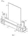
図1を参照すれば、例示液体射出器100は、半導体プロセス技術を用いて作製されたダイ103とすることができる、液体射出モジュール、例えば平行四辺形平板型プリントヘッドモジュールを有する。液体射出器は、以下でさらに論じられる、ダイ103に重なる集積回路インターポーザ104及び下部ハウジング322をさらに有する。ハウジング110が、ダイ103,集積回路インターポーザ104及び下部ハウジング322を支持して、囲み、ハウジング110はハウジング110をプリントバーに連結するためのピン152を有する取付けフレーム142を備えることができる。外部プロセッサからデータを受け取り、ダイに駆動信号を送るための、フレキシブル回路201をダイ103に直接接続することができ、ハウジングによって所定の場所に保持することができる。ダイ103に液体を供給するために下部ハウジング322内部の流入チャンバ132及び流出チャンバ136(図4を見よ)に配管162及び166を連結することができる。液体射出器100から射出される液体はインクとすることができるが、液体射出器100はその他の液体、例えば、生物学的液体、ポリマー、または電子コンポーネントを形成するための液体にも適し得る。
Referring to FIG. 1, an exemplary
図2を参照すれば、液体射出器100は、基板122,例えばダイ103の一部である絶縁体上シリコン(SOI)ウエハ、及び集積回路インターポーザ104を有することができる。集積回路インターポーザ104は、トランジスタ202(図2には射出デバイスが1つしか示されておらず、したがってトランジスタは1つしか示されていない)を有し、ノズル126からの液体の射出を制御するための信号を与えるように構成される。基板122及び集積回路インターポーザ104の内部には複数の液体流路(液路)124が形成されている。単液路124にはポンピングチャンバ174につながる流入チャネル176がある。ポンピングチャンバ174はノズル126及び流出チャネル172の両者につながる。液路124は、ポンピングチャンバ174を流入チャネル176及び流出チャネル172にそれぞれ連結する、ポンピングチャンバ流入口276及びポンピングチャンバ流出口272をさらに有する。液路は半導体プロセス技術、例えばエッチングによって形成することができる。いくつかの実施形態において、ダイ103の層内にある程度まで延びるかまたは層を完全に貫通する直壁構造を形成するために反応性深イオンエッチングが用いられる。いくつかの実施形態において、絶縁層284に隣接するシリコン層286が絶縁層をエッチ止めとして用いて貫通エッチングされる。ダイ103は、ポンピングチャンバ174の1つの壁を定め、ポンピングチャンバ174の内部をアクチュエータへの露出から封止する、メンブラン180を有することができる。絶縁層284のポンピングチャンバ174とは逆の側にノズル層184を配することができる。メンブラン180はシリコンの単層で形成することができる。あるいは、メンブラン180は1つまたはさらに多くの酸化物層を含むことができ、あるいは酸化アルミニウム(Al2O3)、窒化アルミニウムまたは酸化ジルコニウム(ZrO2)で形成することができる。
Referring to FIG. 2, the
液体射出器100は、基板122によって支持される、個別制御可能なアクチュエータ401も有する。複数のアクチュエータ401がアクチュエータ層324(図3を見よ)を形成するとされ、アクチュエータ層324においてアクチュエータは相互に電気的及び物理的に隔てられているが、それでも、層の一部である。基板122は、必要に応じて、アクチュエータとメンブラン180の間に、酸化物のような、絶縁材料282の層を有する。起動されると、アクチュエータは対応する液路124のノズル126から液体を選択的に射出させる。アクチュエータ401が付随する液路124のそれぞれが個別制御可能なMEMS液体射出器ユニットを提供する。いくつかの実施形態において、アクチュエータ401の起動は、メンブラン180をポンピングチャンバ174内に偏向させ、ポンピングチャンバ174の容積を減じさせて、液体をノズル126から押し出す。アクチュエータ401は圧電アクチュエータとすることができ、下部電極190,圧電層192及び上部電極194を有することができる。あるいは、液体射出素子は加熱素子とすることができる。
The
図3に示されるように、液体射出器100は縦積みされた複数の層を有することができる。下部ハウジング322は集積回路インターポーザ104に接合することができる。集積回路インターポーザ104はアクチュエータ層324に接合することができる。アクチュエータ層324はメンブラン180に取り付けることができる。メンブラン180はポンピングチャンバ層326に取り付けることができる。ポンピングチャンバ層326はノズル層184に取り付けることができる。一般に、層は同様の材料を含むかまたは同じ面に沿って存在する同様の素子を有する。層の全てはほぼ同じ幅を有することができ、例えば、それぞれの層は長さ及び長さの少なくとも80%の幅、及び液体射出器100の他の層の幅を有することができる。図3には示されていないが、ハウジング110は縦積みされた層を少なくともある程度囲むことができる。
As shown in FIG. 3, the
図4を参照すれば、液体は、液体供給源から下部ハウジング322を流過し、集積回路インターポーザ104を流過し、基板103を流過して、ノズル層184のノズル126から流出することができる。下部ハウジング322は、分界壁130によって分割して、流入チャンバ132及び流出チャンバ136を設けることができる。液体供給源からの液体は液体流入チャンバ132に流入し、下部ハウジング322の床にある液体流入口101を流過し、下部ハウジング322の液体流入路476を流過し、液体射出モジュール103の液路124を流過し、下部ハウジング322の液体流出路472を流過し、流出口102を通って流出し、流出チャンバ136に流入して、液体回収槽に流れる。液体射出モジュール103を流過している液体の一部をノズル126から射出することができる。
Referring to FIG. 4, liquid may flow from the liquid supply through the
液体流入口101及び液体流入路476はそれぞれ、1つ、2つまたはさらに多くのユニット列のような、多くのMEMS流体射出ユニットの平行流入チャネル176に共通に液体流通可能な態様で連結される。同様に、液体流出口102及び液体流出路472はそれぞれ、1つ、2つまたはさらに多くのユニット列のような、多くのMEMS流体射出ユニットの平行流出チャネル172に共通に液体流通可能な態様で連結される。液体流入チャンバ132のそれぞれは複数の液体流入口101に共通である。また、液体流出チャンバ136のそれぞれは複数の液体流出口102に共通である。
The
図5を参照すれば、ノズル層184はノズル126のマトリックスまたはアレイを有することができる。いくつかの実施形態において、ノズル126は直線平行行504及び直線平行列502に配列される。本明細書で用いられるように、列は、印刷方向に垂直であるよりも印刷方向に平行な軸に近付けて配列されたノズルのセットである。しかし、列502は印刷方向に正確に平行である必要はなく、むしろ45°より小さい角度でオフセットされるであろう。さらに、行は、印刷方向に平行であるよりも印刷方向に垂直な軸に近付けて配列されたノズルのセットである。同様に、行504は印刷方向に正確に垂直である必要はなく、むしろ45°より小さい角度でオフセットされるであろう。列502はノズル層184の幅Wにほぼ沿って延びることができ、行504はノズル層184の長さLにほぼ沿って延びることができる。
Referring to FIG. 5, the
マトリックス内の列502の数は、行504の数より多くすることができる。例えば、20より少ない行及び50より多い列、例えば18行及び80列があり得る。それぞれの行504のノズル126はその行内の隣のノズルとの間隔を等しくすることができる。同様に、それぞれの列のノズル126はその列内の隣のノズルとの間隔を等しくすることができる。さらに、行及び列は垂直方向に揃えられる必要はない。それどころか、行と列の間の角度を90°より小さくすることができる。行及び/または列は完全に間隔をとる必要はないであろう。さらに、ノズル126は行及び/または列をなして直線に沿って配される必要はないであろう。
The number of
ノズルマトリックスは、1平方インチ(6.25cm2)より小さい面積内に、例えば550本と60000本の間のノズル、例えば1440本または1200本のノズルを有する、高密度マトリックスとすることができる。以下でさらに論じられるように、この高密度マトリックスは、例えば、別付けの集積回路インターポーザ104がアクチュエータを制御するためのロジックを有し、ポンピングチャンバ、したがってノズルを相互にさらに密接に近づけることができるから、達成することができる。すなわち、メンブランにかけて通る電気配線をメンブラン層から実質的に無くすことができる。
The nozzle matrix can be a high density matrix having, for example, between 550 and 60000 nozzles, for example 1440 or 1200 nozzles, in an area less than 1 square inch (6.25 cm 2 ). As will be discussed further below, this high density matrix can, for example, have logic for the separate
ノズル126を有する領域は1インチ(25.4mm)より大きい長さLを有することができ、ノズル層の長さLは例えば約34mmとすることができ、またノズル層の幅Wは1インチより小さく、例えば約6.6mmとすることができる。ノズル層は20μm〜40μmのような、1μmと50μmの間の、例えば30μmの、厚さを有することができる。ノズル126はKOHでエッチングすることができ、正方形または円形とすることができる。
The region with the
媒体がプリントバーの下方を通過するときに、高密度マトリックスのノズルは、媒体上にピクセルの線を、600dpiより高い、1200dpi以上のような、高密度、すなわち高印刷解像度で、形成するために、単パスで媒体上に液体を射出することができる。1200dpi以上の密度を得るため、大きさが0.01pLと10pLの間の、2pLのような液滴をノズルから射出することができる。ノズルの幅は10μmと20μmの間のような、1μmと20μmの間、例えば約15μmまたは15.6μmとすることができる。 As the media passes under the print bar, the high density matrix nozzles form pixel lines on the media at a high density, i.e., high print resolution, such as higher than 600 dpi and higher than 1200 dpi. The liquid can be ejected onto the medium in a single pass. In order to obtain a density of 1200 dpi or more, droplets such as 2 pL with a size between 0.01 pL and 10 pL can be ejected from the nozzle. The width of the nozzle can be between 1 μm and 20 μm, such as between about 10 μm and 20 μm, for example about 15 μm or 15.6 μm.
ノズル層184はシリコンで形成することができる。別の実施形態において、ノズル層184はポリイミドまたは、エッチングが必要とされないフォトリソグラフィでパターンを形成できる点で有利になり得る、フォトポリマー、ドライフィルムフォトレジストまたは感光性ポリイミドのような、感光性フィルムで形成することができる。
The
図6を参照すれば、ノズル層184にポンピングチャンバ層326を隣接させる、例えば取り付けることができる。ポンピングチャンバ層326はポンピングチャンバ174を有する。それぞれのポンピングチャンバ174は付随するノズルから液体を押し出す変形可能な壁を少なくとも1つもつ空間とすることができる。ポンピングチャンバは可能な最大の実装密度を提供する形状をとることができる。図6に示されるように、ポンピングチャンバ174はほぼ円形であり、一般に側壁602よって定めることができる。ポンピングチャンバは正確な円形ではなく、すなわち準円形であり、楕円形、または長円形とすることができ、あるいは六角形、八角形または多角形のような、直辺と曲辺の組合せを有することができる。さらに、ポンピングチャンバは、最長幅に沿って、約125μmから250μmのような、約100μmから400μmとすることができる。ポンピングチャンバ174の高さはポンピングチャンバの最短幅の50%未満とすることができる。
Referring to FIG. 6, a
それぞれのポンピングチャンバは、ポンピングチャンバから延び、ポンピングチャンバ層326に形成された、ポンピングチャンバ流入口276及びポンピングチャンバ流出口272を有することができる。ポンピングチャンバ流入口276及びポンピングチャンバ流出口272はポンピングチャンバ174と同じ平面に沿って延びることができ、互いに同じ軸に沿って通ることができる。ポンピングチャンバ流入口276及びポンピングチャンバ流出口272はポンピングチャンバ174よりかなり狭い幅を有することができ、この幅は流入口または流出口の最小平面寸法である。ポンピングチャンバ流入口276及びポンピングチャンバ流出口272の幅はポンピングチャンバ174の幅の30%未満、例えば10%未満とすることができる。ポンピングチャンバ流入口276及びポンピングチャンバ流出口272はポンピングチャンバ174から延びる平行壁を有することができ、平行壁間の距離が幅である。図6Aに示されるように、ポンピングチャンバ流入口276の形状はポンピングチャンバ流出口272と同じとすることができる。
Each pumping chamber may have a pumping
ポンピングチャンバ層はポンピングチャンバ流入口276及びポンピングチャンバ流出口272並びに流入チャネル176及び流出チャネル172から独立なチャネルを有していない。言い換えれば、ポンピングチャンバ流入口276及びポンピングチャンバ流出口272を除いて、ポンピングチャンバ層を水平方向に通る液路はない。同様に、流入チャネル176及び流出チャネル172を除いて、ポンピングチャンバ層を垂直方向に通る液路はない。ポンピングチャンバ層326は下降流路、すなわちポンピングチャンバ174からノズル126に通るチャネルを有していない。それどころか、ポンピングチャンバ174はノズル層184のノズル126に直接に接する。さらに、流入チャネル176はダイ103をほぼ垂直方向に通ってポンピングチャンバ流入口276と交差する。ポンピングチャンバ流入口276は続いてポンピングチャンバ層326を水平方向に通ってポンピングチャンバ174と液体流通可能な態様で連結する。同様に、流出チャネル172はダイ103をほぼ垂直方向に通ってポンピングチャンバ流出口272と交差する。
The pumping chamber layer does not have a channel independent of the pumping
図6Aに、平面図で、示されるように、液体流入口176と交差するポンピングチャンバ流入口276の領域676及び液体流出口172と交差するポンピングチャンバ流出口272の領域672はポンピングチャンバ流入口276及びポンピングチャンバ流出口272の残余領域よりも幅を広くするかまたは直径を大きくすることができる。さらに、領域672及び676はほぼ円形の形状をとることができる。すなわち、流入チャネル176及び流出チャネル172はチューブ形状をとることができる。さらに、付随するノズル126は、ポンピングチャンバ174の直下に配して、ポンピングチャンバ174と中心を合わせることができる。
In FIG. 6A, as shown in plan view, a
図6に戻って参照すれば、ポンピングチャンバ174は行と列を有するマトリックスに配列することができる。列と行の間の角度は90°より小さくすることができる。1つのダイに、550と60000の間の数のポンピングチャンバを入れることができ、例えば1平方インチより小さい面積に1440または1200の数のポンピングチャンバを入れることができる。ポンピングチャンバの高さは50μm未満、例えば25μmとすることができる。さらに、図2に戻って参照すれば、それぞれのポンピングチャンバ174は対応するアクチュエータ401と隣接する、例えば、アクチュエータ401と位置を合わせて直下に配されることができる。ポンピングチャンバは対応するアクチュエータからノズルまでの距離の少なくとも80%の距離にわたって延びることができる。
Referring back to FIG. 6, the pumping
ノズル層184と同様、ポンピングチャンバ層26はシリコンまたは感光性フィルムで形成することができる。感光性フィルムは、例えば、フォトポリマー、ドライフィルムフォトレジストまたは感光性ポリイミドとすることができる。
Similar to the
メンブラン層180を、ポンピングチャンバ層326に隣接させる、例えば取り付けることができる。図7を参照すれば、メンブラン層180はメンブラン層180を貫通する開口702を有することができる。開口は液路124の一部とすることができる。すなわち、流入チャネル176及び流出チャネル172は、メンブラン層180の開口702を通って延びることができる。したがって開口702は行と列を有するマトリックスを形成することができる。メンブラン層180は、例えばシリコンで形成することができる。メンブランは25μm未満のように比較的薄く、例えば約12μmとすることができる。
The
アクチュエータ層324を、メンブラン層180に隣接させる、例えば取り付けることができる。アクチュエータ層はアクチュエータ401を有する。アクチュエータは加熱素子とすることができる。あるいは、アクチュエータ401は、図2,8及び9に示されるように、圧電素子とすることができる。
The
図2,8及び9に示されるように、それぞれのアクチュエータ401は、下部電極190及び上部電極194を含む、2つの電極の間の圧電層192を有する。圧電層192は例えばチタン酸鉛ジルコニウム(PZT)膜とすることができる。圧電層192の厚さは、約1μmと4μmの間のように、約1μmと25μmの間とすることができる。圧電層192はバルク圧電材料で形成することができ、あるいは物理的気相成長装置を用いるスパッタリングによるかまたはゾル−ゲル法によって形成することができる。スパッタ圧電層は柱状構造をとり得るが、バルク圧電層及びゾル−ゲル圧電層はよりランダムな構造をとり得る。いくつかの実施形態において、圧電層192は、図8に示されるように、全てのアクチュエータの面内及び間にわたって拡がる連続圧電層である。あるいは、図2及び9に示されるように、圧電層は、隣り合うアクチュエータの圧電領域が相互に接触しないように、例えば隣り合うアクチュエータを分離する間隙が圧電層にあるように、セグメントに分けることができる。例えば、圧電層192はほぼ円形につくられた島構造とすることができる。個々に形成された島構造はエッチングで作製することができる。図2に示されるように、圧電層192が連続ではない場合に上部電極と下部電極の相互接触を防止するために、絶縁物層、例えばSU8または酸化物の層のような、底面保護層214を用いることができる。以降の処理工程中にアクチュエータを保護するため、及び/またはモジュールの動作中に水分からアクチュエータを保護するため、絶縁物層、例えばSU8または酸化物の層のような、上面保護層210を用いることができる。
As shown in FIGS. 2, 8 and 9, each
いくつかの実施形態では駆動電極層である、上部電極194は導電材料で形成される。駆動電極として、上部電極194は、液体射出サイクル中の適切な時点に圧電層194にかけて電圧差を供給するために、コントローラに接続される。上部電極194はパターン形成された導電層を有することができる。例えば、図8及び9に示されるように、上部電極194はリング電極とすることができる。あるいは、上部電極194は中央電極または内部電極及びリング電極をともに組み込んでいる二重電極とすることができる。
In some embodiments, the
いくつかの実施形態では基準電極層である、下部電極190は導電材料で形成される。下部電極は接地することができる。下部電極はメンブラン層180に直接にパターン形成することができる。さらに、下部電極190は、図8及び9に示されるように、複数のアクチュエータに共通とすることができて、複数の電極にかけて拡がることができる。上部電極194及び下部電極190は、金、ニッケル、ニクロム、銅、イリジウム、酸化イリジウム、白金、チタン、チタン-タングステン、酸化インジウムスズまたはこれらの組合せで形成することができる。本実施形態において、保護層210及び214は連続層であり、ポンピングチャンバ174に重なる孔及びリード222を有することができる。そのような構成においては、図2に示されるように、保護層210及び214はアクチュエータ401のまわりだけに配置することができる。図8に示されるように、接地接続のために圧電層192を貫通する接地開口812を形成することができる。あるいは、図9に示されるように、下部電極190に沿って、例えば下部電極190のアクチュエータ層324の長さLに平行に通る部分に沿って、どこででも接地接続がなされ得るようにPZTをエッチング除去することができる。
In some embodiments, the
圧電層192は、上部電極194と下部電極190の間で圧電層192にかけて印加される電圧に応答して形状寸法を変えることができる。圧電層195の形状寸法変化によりメンブラン180が撓み、続いてポンピングチャンバ175の容積が変わり、ポンピングチャンバ内の液体に圧力がかかって、制御可能な態様でノズル126を通して液体を押し出す。
The
図8に示されるように、アクチュエータ層324はさらに、以下で論じられるように、フレキシブル回路への接続のための入力電極810を有することができる。入力電極810はアクチュエータ層324の長さLに沿って延びる。入力電極810は、アクチュエータ層324の、上部電極194及び下部電極190と同じ表面に沿って配置することができる。あるいは、入力電極810はアクチュエータ層324の辺に沿って、例えば集積回路インターポーザ104への接合される表面に対して垂直な細長い表面上に、配置することができるであろう。
As shown in FIG. 8, the
図8及び9を参照すれば、圧電素子401は行と列からなるマトリックスに配列することができる(他の素子をさらに明瞭に示すことができるように、圧電素子401はいくつかしか示されていない)。開口802がアクチュエータ層324を貫通することができる。開口802は液路124の一部とすることができる。すなわち、流入チャネル176及び流出チャネル172はアクチュエータ層324の開口802を通って延びることができる。図2及び8に示されるように、圧電材料がエッチング除去されていれば、開口802を形成するため、メンブラン層180と集積回路インターポーザ104の間に、SU8のような、バリア材料806を配置することができる。言い換えれば、バリア材料806は、開口802がそれを通して延びることができる、バンプとして形成することができる。以下で論じられるように、バリア材料806は、圧電層が中実層である場合に、図9に示されるように、電子素子を液漏れから保護するための封止材としてはたらかせるために用いることもできるであろう。以下でさらに論じられるように、アクチュエータ層324はアクチュエータ401のまわりを通る配線または電気接続を有していない。それどころか、アクチュエータを制御する配線は集積回路インターポーザ104に配置される。
8 and 9, the
集積回路インターポーザ104はアクチュエータ層401に隣接させることができ、いくつかの例ではアクチュエータ層401に取り付けることができる。集積回路インターポーザ104はアクチュエータ401の動作を制御するための信号を与えるように構成される。図10を参照すれば、集積回路インターポーザ104は、例えば半導体製造技術によって、集積回路が形成されているマイクロチップとすることができる。いくつかの実施形態において、集積回路インターポーザ104は特定用途集積回路(ASIC)素子である。集積回路インターポーザ104はアクチュエータ制御信号を与えるためのロジックを有することができる。
The
図10をまだ参照すれば、集積回路インターポーザ104は複数の、トランジスタのような、集積スイッチング素子202を有することができる。集積スイッチング素子202は行と列からなるマトリックスに配列することができる。一実施形態において、アクチュエータ401毎に集積スイッチング素子202が1つある。2つの集積回路素子202を備えれば、所要電圧が1/2になるように、第1のトランジスタで対応するアクチュエータの一部分を駆動し、第2のトランジスタでそのアクチュエータの別の部分を駆動するための、あるいは単トランジスタよりも複雑な波形を可能にするようなアナログスイッチをつくるための、冗長性を提供するために有益であり得る。さらに、4つの集積回路素子202を用いれば、冗長アナログスイッチを得ることができる。単集積回路素子202または複数の集積回路素子202は、対応するアクチュエータ401に隣接して、または対応するアクチュエータ401の上に、配置することができる。すなわち、ノズル126を通り、ポンピングチャンバ174を通り、トランジスタをまたは2つのスイッチング素子の間を通って、軸が延びることができる。それぞれのスイッチング素子202は、アクチュエータ401の内の1つの上部電極194を駆動信号源に選択的に接続するためのオン/オフスイッチとしてはたらく。駆動信号電圧は集積回路インターポーザ104の内部ロジックによって伝えられる。
Still referring to FIG. 10, the
集積回路インターポーザ104の集積スイッチング素子202,例えばトランジスタはリード222a、例えば金バンプを介してアクチュエータ401に接続することができる。集積回路インターポーザ104の縁に沿ってリード222b、例えば金バンプ、の群を配列することができる。それぞれの群は多くのリード222b、例えば3つのリード222bを含むことができる。集積スイッチング素子202の列毎に1つのリード222b群があり得る。リード222bは集積回路インターポーザ104のロジックを、例えばアクチュエータ層324の接地開口812を通して、ダイ103上の接地電極190に接続するように構成することができる。さらに、集積回路インターポーザ104の縁の近傍にリード222c、例えば金バンプを配置することができる。リード222cは、以下で論じられるように、集積回路インターポーザ104のロジックをフレキシブル回路201との接続のための入力電極810に接続するように構成することができる。リード222a,222b,222cは基板の、ポンピングチャンバに重ならない、領域に配置される。
The
図10に示されるように、集積回路インターポーザ104は、集積回路インターポーザ104を貫通する、開口902を有することができる。この開口は、層の電気接続のための余地を残すために、集積回路インターポーザ104の集積スイッチング素子202を有する側の近傍で、反対側よりも狭くすることができる。開口902は液路124の一部とすることができる。すなわち、流入チャネル176及び流出チャネル172は、集積回路インターポーザ104の開口902を通って延びることができる。液路124と、集積回路インターポーザ104のロジックのような、電子素子/回路の間の液漏れを防止するため、液路124は、良好な酸素バリアを提供し、液路を通す流体の輸送を容易にするために良好な濡れ特性を有する、金属、例えばチタンまたはタンタル、あるいは非金属材料、例えば、酸化シリコン、減圧化学的気相成長(LPCVD)酸化物、酸化アルミニウム、または窒化シリコン/酸化シリコンのような、材料で被覆することができる。被覆は、電気メッキ、スパッタリング、CVDまたはその他の堆積プロセスによって施すことができる。さらに、集積回路素子のロジックを液漏れから保護するためにバリア材料806を用いることができる。別の実施形態において、集積回路インターポーザ104とダイ103の間に、スピンコーティングによるように、バリア層、例えばSU8を配することができるであろう。バリア層は、集積回路インターポーザ104及びダイ103の長さ及び幅の全て、またはほぼ全てにかけて、拡がることができ、開口902の開口を残すようにパターンを形成することができる。
As shown in FIG. 10, the
液体射出器100はさらにフレキシブルプリント回路すなわちフレキシブル回路201を有することができる。フレキシブル回路201は、例えばプラスチック基板上に形成することができる。フレキシブル回路201は液体射出器100をプリンタシステムまたはコンピュータ(図示せず)に電気的に接続するように構成される。フレキシブル回路201は、液体射出素子、例えばアクチュエータ401を駆動するためにダイ103に、プリンタシステムの外部プロセスのための、画像データ及びタイミング信号のような、データを送るために用いられる。
The
図11及び12に示されるように、フレキシブル回路201は、接着剤、例えばエポキシ樹脂によるように、アクチュエータ層324に接合することができる。一実施形態において、図11に示されるように、アクチュエータ層324は集積回路インターポーザ104の幅wより広い幅Wを有することができる。したがってアクチュエータ層324は集積回路インターポーザ104から張り出して、レッジ912を形成することができる。フレキシブル回路201は、アクチュエータ層324に接触している表面に対して直交する集積回路インターポーザ104の縁端がフレキシブル回路201に平行に延びるように、集積回路インターポーザ104の横に延びることができる。フレキシブル回路201は厚さtを有する。フレキシブル回路201は厚さtよりかなり大きな高さ及び幅を有することができる。例えば、フレキシブル回路201の幅はほぼ、33mmのような、ダイの長さとすることができ、厚さtは12μmと100μmの間のような、25〜50μmのような、100μm未満、例えばほぼ25μmとすることができる。例えば厚さtを有する、最も狭い縁端をアクチュエータ層324の上面に、例えば集積回路インターポーザ104に接合されるアクチュエータ層324の表面に、接合することができる。
As shown in FIGS. 11 and 12, the
図12に示される別の実施形態において、集積回路インターポーザ104はダイのアクチュエータ層324の幅Wより広い幅wを有することができる。したがって、集積回路インターポーザ104はアクチュエータ層324から張り出して、レッジ914を形成することができる。フレキシブル回路201はインターポーザ104への取付けのために曲がってレッジ94を回り込むことができる。すなわち、フレキシブル回路201は、アクチュエータ層324に接している表面に直交する集積回路インターポーザ104の縁端がフレキシブル回路201の一部に平行に延びるように、集積回路インターポーザ104の横に延びることができる。フレキシブル回路201は、フレキシブル回路201の一部が集積回路インターポーザ104の底面、すなわちアクチュエータ層324に接する表面に、取り付くように、曲がってレッジ194をも回り込むことができる。図11に示される実施形態と同様に、フレキシブル回路は厚さtよりかなり大きい高さ及び幅を有することができる。例えば、フレキシブル回路201の幅はほぼ、33mmのような、ダイの長さとすることができ、厚さtは12μmと100μmの間のような、25〜50μmのような、100μm未満、例えばほぼ25μmとすることができる。例えば厚さtを有する、最も狭い縁端は、アクチュエータ層324に、例えば集積回路インターポーザ104に接合されるアクチュエータ層324の表面に直交するアクチュエータ層324の表面に隣接することができる。
In another embodiment, shown in FIG. 12, the
図示されてはいないが、フレキシブル回路201は安定性のために基板103に隣接することができる。フレキシブル回路201はアクチュエータ層324上の入力電極810に電気的に接続することができる。ハンダのような、導電材料の小さなビードを用いて、フレキシブル回路201を入力電極に電気的に接続することができる。最後に、流体射出器100毎にフレキシブル回路は1つしか必要ではない。
Although not shown, the
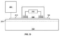
フレキシブル回路201,集積回路インターポーザ104及びダイ103の接続図が図13に示される。フレキシブル回路201からの信号は、入力電極810を介して送り出され、リード222cを介して集積回路インターポーザ104に送られて、集積回路素子202におけるように、集積回路インターポーザ104上で処理され、リード222aに出力されてアクチュエータ401の上部電極194を賦活し、よってアクチュエータ401を駆動する。
A connection diagram of the
集積回路素子222には、データフリップフロップ、ラッチフリップフロップ、ORゲート及びスイッチを含めることができる。集積回路インターポーザ104のロジックは、クロック線、データ線、ラッチ線、オール-オン線及び電力線を有することができる。データ線を介してデータフリップフロップにデータを送ることによって信号が処理される。次いでデータが入力されるとクロック線がデータをクロックする。データは、第1のフリップフロップに入力されたデータのダイ1ビットが、データの次のビットが入力されるとシフトダウンされるように、シリアルに入力される。データフリップフロップの全てがデータを得た後、データをデータフリップフロップからラッチフリップフロップに移し、液体射出素子401上に送るために、ラッチ線を介してパルスが送られる。ラッチフリップフロップからの信号が「ハイ」であれば、スイッチはオンになり、液体射出素子401を駆動するために信号を通過させる。信号が「ロー」であれば、スイッチはオフのままであり、流体射出素子401は起動されない。
Integrated circuit element 222 can include data flip-flops, latch flip-flops, OR gates, and switches. The logic of the
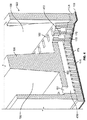
上述したように、液体射出器100はさらに、図14に示される下部ハウジング322を有することができる。液体流入口101及び液体流出口102が下部ハウジング322の長さlに沿う2本の平行液路で延びることができる。それぞれの、すなわち液体流入口101または液体流出口102の、液路は下部ハウジング322の端近くを延びることができる。
As described above, the
縦方向液体流入口101は下部ハウジング322の横方向液体流入路476につながることができる。同様に、縦方向流体流出口102は下部ハウジング322の(図14には示されていない)横方向液体流出路472につながることができる。液体流入路476及び液体流出路472は相互に同じ形状及び容積とすることができる。液体流入路及び液体流入口は合わせて概ね「L」字形とすることができる。さらに、液体流入路476及び液体流出路472のそれぞれは、下部ハウジング322の幅wにかけて相互に平行に通り、例えばハウジングコンポーネントの、80〜95%のような、70〜90%にかけて、またはハウジングコンポーネントの幅の85%にかけて、延びる。さらに、液体流入路476及び液体流出路472は下部ハウジング322の長さlにかけて交互することができる。
The vertical
液体流入路476及び液体流出路472はそれぞれ同じ方向に、すなわち平行な軸に沿って、延びることができる。さらに、図4に示されるように、液体流入路476はそれぞれ複数の液体流入チャネル176に連結することができる。それぞれの液体流入チャネル176は液体流入路476から直交方向に延びることができる。同様に、液体流出路472はそれぞれ複数の液体流出チャネル172に連結することができ、液体流出チャネル172のそれぞれは液体流出路472から直交方向に延びることができる。
The
したがって、液体供給源からの液体は、液体流入チャンバ132に流れ込み、ハウジング132の液体流入口101を流過し、下部ハウジング322の液体流入路476を流過し、液体射出モジュール103の複数の液路を流過し、下部ハウジング322の液体流出路472を流過し、流出口102を通って流れ出て、流出チャンバ136に流入し、液体回収槽に流れる。
Accordingly, the liquid from the liquid supply source flows into the
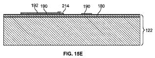
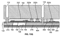
図15A〜15Tは液体射出器100を作製するための方法の一例を示す。メンブラン180を有するウエハ122(図15Aを見よ)上,例えば酸化物上シリコン(SOI)ウエハのような半導体ウエハ上に下部電極190をスパッタする。次いで圧電層192を下部電極190に重ねてスパッタして(図15Bを見よ)、エッチングする(図15Cを見よ)。下部電極190をエッチングして(図15Dを見よ)、底面保護層214を施すことができる(図15Eを見よ)。次いで上部電極194をスパッタしてエッチングすることができて(図15Fを見よ)、上面保護層210を施すことができる(図15Gを見よ)。次いで、液路124を液漏れから保護するためのバリア材料806を施し、バリア材料806を通る開口802を形成することができる(図15Hを見よ)。次いで開口702を、開口702の位置が開口802の位置と揃うように、メンブラン層180にエッチングすることができる(図15Iを見よ)。必要に応じて、酸化物層288をエッチング止めとして用いることができる。
15A-15T illustrate an example of a method for making the
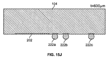
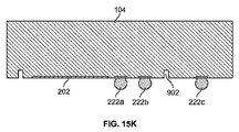
集積回路素子202及びリード222a,222b,222cをもつ集積回路インターポーザ104,例えばASICウエハを形成することができる(図15Jを見よ)。図15K及び15Lに示されるように、開口902を、例えば反応性深イオンエッチングを用いて、集積回路インターポーザ104にエッチングして、液路部分を形成することができる。開口902は、初めに集積回路インターポーザ104の底面、すなわち集積回路素子202を有する表面にエッチングすることができる(図15Kを見よ)。開口902は次いで、集積回路インターポーザ104の上面から大径孔をエッチングすることによって完成することができる(図15Lを見よ)。大径孔によりエッチングプロセスが容易になり、開口902を液体により腐蝕から保護するための保護材料層を開口902の側壁にスパッタリングで形成することが可能になる。
An
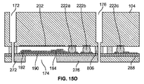
エッチングに続いて、BCBまたはポリイミドまたはエポキシ樹脂のような、スピンオンした接着剤を用いて、集積回路インターポーザ104とウエハ122を接合することができる(図15Mを見よ)。あるいは、接着剤は集積回路インターポーザ104及びウエハ122上にスプレーすることができる。集積回路インターポーザ104とウエハ122の接合は、集積回路インターポーザの開口902の位置,ポンピングチャンバ層の開口802の位置及びメンブラン層180の開口802の位置が合わせられて、液体流入チャネル176及び液体流出チャネル172が形成されるように、行われる。
Following etching, the
次いで、ウエハ122を研削及び研磨してハンドリング層601を形成することができる(図15Nを見よ)。図示していないが、研削中は集積回路インターポーザ104を保護する必要があろう。ポンピングチャンバの流入口276及び流出口172を含む、ポンピングチャンバ174をウエハ122の底面から、すなわち集積回路インターポーザ104とは逆の面に、エッチングすることができる(図15Oを見よ)。必要に応じて、酸化物層288をエッチング止めとして用いることができる。既にノズル126がノズル層184にエッチングでつくり込まれているノズルウエハ608を次いで、BCBのような、エポキシ樹脂を用いる接合のような、低温接合形成法を用いるか、または低温プラズマ活性化接合形成法を用いて、ウエハ122に接合することができる(図15Pを見よ)。例えば、ノズル層は、既に構造体に接合されている圧電層192を損なわないように、約200℃と300℃の間の温度でウエハ122に接合することができる。次いでノズルウエハ608のノズルハンドリング層604を、必要に応じて酸化物層284をエッチング止めとして用いて、研削及び研磨によって形成することができる(図15Qを見よ)。この場合も、図示していないが、研削中は集積回路インターポーザ104を保護する必要があろう。次いで、酸化物層284を除去することによってノズルを開けることができる(図15Rを見よ)。上述したように、ノズル層184及びポンピングチャンバ326は感光性フィルムで形成することもできる。
The
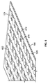
最後に、ウエハを単位に分割する、すなわち多くのダイ103、例えば形状が長方形、平行四辺形または台形のダイ、に切り分けることができる(図16を見よ)。図16に示されるように、液体射出器100のダイ103は十分に小さく、例えば幅がほぼ5〜6mmで長さが30〜40mmであり、よって少なくとも300のポンピングチャンバを有するダイを150mm径ウエハ上に少なくとも40個形成できる。例えば、図16に示されるように、1枚の200mm径ウエハから88個のダイ103を形成することができる。次いでフレキシブル回路201を液体射出器に取り付けることができる(図15Tを見よ)。
Finally, the wafer can be divided into units, i.e., many dies 103, such as rectangular, parallelogram or trapezoidal dies (see FIG. 16). As shown in FIG. 16, the
本明細書に説明される作製工程は、挙げられた順序で実施する必要はない。作製はより多くのシリコンを有する液体射出器より低費用になり得る。 The fabrication steps described herein need not be performed in the order listed. Fabrication can be less expensive than a liquid ejector with more silicon.
本明細書に説明されるような、例えば、ポンピングチャンバとノズルの間に下降流路がなく、ダイのアクチュエータの射出を制御するためのロジックをダイから隔てる層を有し、ダイではなくハウジングに液体流入路及び液体流出路を有する、液体射出器100は、低コストとすることができ、高品質画像を印刷することができ、高速で印刷することができる。例えば、ポンピングチャンバとノズルの間に下降流路がないことで、液体は層を迅速に通過することができ、よって低い、例えば、17Vのような、20V未満の駆動電圧を用い、高い、例えば180kHzから390kHzの周波数での液体の射出が可能になる。同様に、ポンピングチャンバ層に上昇流路がないことで、ポンピングチャンバ層を薄くすることができる。そのような構造により、幅が15μmより広いノズルから大きさが2pLないしさらに小さい液滴が可能になる。
As described herein, for example, there is no downflow path between the pumping chamber and the nozzle, and there is a layer separating logic from the die to control the firing of the die actuator, so that the housing is not the die. The
さらに、基板上ではなく集積回路インターポーザにロジックを有することで、基板上の配線及び電気接続を少なくすることができ、よって高密度ポンピングチャンバ/ノズルマトリックスを形成することができる。同様に、ポンピングチャンバ層にはポンピングチャンバ流入口及びポンピングチャンバ流出口しかなく、例えば上昇流路がないことで、高密度ポンピングチャンバ/ノズルマトリックスを形成することができる。この結果、印刷媒体上で600dpiをこえる解像度を達成することができ、6インチ(150mm)径ウエハ当たり少なくとも88個のダイを形成することができる。 Furthermore, having logic in the integrated circuit interposer rather than on the substrate can reduce wiring and electrical connections on the substrate, thus forming a high density pumping chamber / nozzle matrix. Similarly, the pumping chamber layer has only a pumping chamber inlet and a pumping chamber outlet, such as no rising channel, so that a high density pumping chamber / nozzle matrix can be formed. As a result, resolutions in excess of 600 dpi can be achieved on the print media, and at least 88 dies can be formed per 6 inch (150 mm) diameter wafer.
基板ではなくハウジングに液体流入路及び液体流出路を有することで、流路間のクロストークを最小限に抑えることができる。最後に、シリコンではなく感光性フィルムを用い、インターポーザのような、余分なシリコンを含めないことで、液体射出器のコストを低く抑えることができる。 By having the liquid inflow path and the liquid outflow path in the housing instead of the substrate, crosstalk between the flow paths can be minimized. Finally, the cost of the liquid ejector can be kept low by using a photosensitive film instead of silicon and not including extra silicon such as an interposer.
特定の実施形態を説明した。その他の実施形態は添付される特許請求の範囲内にある。 A particular embodiment has been described. Other embodiments are within the scope of the appended claims.
100 液体射出器
103 ダイ
104 集積回路インターポーザ
122 基板
124 液体流路(液路)
126 ノズル
172 流出チャネル
174 ポンピングチャンバ
176 流入チャネル
180 メンブラン
184 ノズル層
190 下部電極
192 圧電層
194 上部電極
201 フレキシブル回路
202 スイッチング素子
210 上面保護層
214 底面保護層
222a,222b,222c リード
272 ポンピングチャンバ流出口
276 ポンピングチャンバ流入口
282 絶縁材料
284 絶縁層
286 シリコン層
401 アクチュエータ
806 バンプ材料
810 入力電極
DESCRIPTION OF
126
Claims (15)
複数の液路を有する基板を備える液体射出モジュールであって、前記複数の液路のそれぞれは、ノズルと液体流通可能な態様で連結しているポンピングチャンバ、及び複数の液体射出素子を有し、前記複数の液体射出素子のそれぞれは付随する液路のノズルから液体を射出させるように構成されるものである液体射出モジュール、
及び
前記液体射出モジュール上に搭載され、複数の集積スイッチング素子を有する集積回路インターポーザであって、前記複数の集積スイッチング素子のそれぞれは、前記液体射出モジュールの電気接続によって、前記集積回路インターポーザに送られるべき信号の、前記液体射出モジュールへの送信、前記集積回路インターポーザ上での処理、及び前記複数の液体射出素子の内の少なくとも1つを駆動するための前記液体射出モジュールへの出力が可能になるように、前記液体射出モジュールと電気的に接続されるものである集積回路インターポーザ、
を備えることを特徴とする液体射出器。 In liquid ejector,
A liquid ejection module comprising a substrate having a plurality of liquid paths, each of the plurality of liquid paths having a pumping chamber connected to the nozzle in a manner allowing liquid to flow, and a plurality of liquid ejection elements, Each of the plurality of liquid ejection elements is a liquid ejection module configured to eject liquid from a nozzle of an associated liquid path,
And an integrated circuit interposer mounted on the liquid ejection module and having a plurality of integrated switching elements, each of the plurality of integrated switching elements being sent to the integrated circuit interposer by electrical connection of the liquid ejection module. Enables transmission of power signals to the liquid ejection module, processing on the integrated circuit interposer, and output to the liquid ejection module to drive at least one of the plurality of liquid ejection elements An integrated circuit interposer that is electrically connected to the liquid ejection module,
A liquid ejector comprising:
Applications Claiming Priority (3)
| Application Number | Priority Date | Filing Date | Title |
|---|---|---|---|
| US22484709P | 2009-07-10 | 2009-07-10 | |
| US61/224,847 | 2009-07-10 | ||
| PCT/US2010/040938 WO2011005699A2 (en) | 2009-07-10 | 2010-07-02 | Mems jetting structure for dense packing |
Related Child Applications (1)
| Application Number | Title | Priority Date | Filing Date |
|---|---|---|---|
| JP2015121791A Division JP6128613B2 (en) | 2009-07-10 | 2015-06-17 | MEMS jet injection structure for high-density packaging |
Publications (2)
| Publication Number | Publication Date |
|---|---|
| JP2012532772A true JP2012532772A (en) | 2012-12-20 |
| JP2012532772A5 JP2012532772A5 (en) | 2013-08-15 |
Family
ID=43427143
Family Applications (6)
| Application Number | Title | Priority Date | Filing Date |
|---|---|---|---|
| JP2012519625A Pending JP2012532772A (en) | 2009-07-10 | 2010-07-02 | MEMS jet injection structure for high-density packaging |
| JP2015121791A Active JP6128613B2 (en) | 2009-07-10 | 2015-06-17 | MEMS jet injection structure for high-density packaging |
| JP2017075869A Pending JP2017140847A (en) | 2009-07-10 | 2017-04-06 | Mems jet injection structure for high-density mounting |
| JP2018078230A Pending JP2018140638A (en) | 2009-07-10 | 2018-04-16 | Mems jet injection structure for high-density mounting |
| JP2021126444A Pending JP2021176710A (en) | 2009-07-10 | 2021-08-02 | Mems jetting structure for dense packing |
| JP2023047956A Pending JP2023078404A (en) | 2009-07-10 | 2023-03-24 | Mems jetting structure for dense packing |
Family Applications After (5)
| Application Number | Title | Priority Date | Filing Date |
|---|---|---|---|
| JP2015121791A Active JP6128613B2 (en) | 2009-07-10 | 2015-06-17 | MEMS jet injection structure for high-density packaging |
| JP2017075869A Pending JP2017140847A (en) | 2009-07-10 | 2017-04-06 | Mems jet injection structure for high-density mounting |
| JP2018078230A Pending JP2018140638A (en) | 2009-07-10 | 2018-04-16 | Mems jet injection structure for high-density mounting |
| JP2021126444A Pending JP2021176710A (en) | 2009-07-10 | 2021-08-02 | Mems jetting structure for dense packing |
| JP2023047956A Pending JP2023078404A (en) | 2009-07-10 | 2023-03-24 | Mems jetting structure for dense packing |
Country Status (7)
| Country | Link |
|---|---|
| US (5) | US8820895B2 (en) |
| EP (1) | EP2451647B1 (en) |
| JP (6) | JP2012532772A (en) |
| KR (1) | KR20120040239A (en) |
| CN (1) | CN102481789B (en) |
| HK (1) | HK1167369A1 (en) |
| WO (1) | WO2011005699A2 (en) |
Cited By (13)
| Publication number | Priority date | Publication date | Assignee | Title |
|---|---|---|---|---|
| WO2014185369A1 (en) * | 2013-05-15 | 2014-11-20 | コニカミノルタ株式会社 | Inkjet head and method for producing inkjet head |
| EP2990205A2 (en) | 2014-08-29 | 2016-03-02 | Canon Kabushiki Kaisha | Liquid discharge head and head unit using the same |
| JP2016049675A (en) * | 2014-08-29 | 2016-04-11 | キヤノン株式会社 | Liquid discharge head and method for manufacturing the same |
| JP2016107495A (en) * | 2014-12-05 | 2016-06-20 | キヤノン株式会社 | Liquid discharge head and liquid discharge device |
| US9533503B2 (en) | 2014-08-29 | 2017-01-03 | Canon Kabushiki Kaisha | Liquid ejection head |
| US9616666B2 (en) | 2014-08-29 | 2017-04-11 | Canon Kabushiki Kaisha | Method of manufacturing element substrate |
| US9919521B2 (en) | 2014-08-29 | 2018-03-20 | Canon Kabushiki Kaisha | Liquid ejection head |
| JPWO2017047533A1 (en) * | 2015-09-18 | 2018-07-05 | コニカミノルタ株式会社 | Inkjet head and inkjet recording apparatus |
| JP2018140638A (en) * | 2009-07-10 | 2018-09-13 | フジフィルム ディマティックス, インコーポレイテッド | Mems jet injection structure for high-density mounting |
| US10232616B2 (en) | 2016-12-06 | 2019-03-19 | Canon Kabushiki Kaisha | Liquid ejection head |
| US10647117B2 (en) | 2017-05-29 | 2020-05-12 | Seiko Epson Corporation | Piezoelectric device, liquid discharging head, and liquid discharging apparatus |
| US10875305B2 (en) | 2018-04-17 | 2020-12-29 | Canon Kabushiki Kaisha | Liquid ejection head |
| JP2022046802A (en) * | 2016-01-08 | 2022-03-23 | キヤノン株式会社 | Liquid discharge head and liquid discharge device |
Families Citing this family (33)
| Publication number | Priority date | Publication date | Assignee | Title |
|---|---|---|---|---|
| US8297742B2 (en) * | 2010-03-19 | 2012-10-30 | Fujifilm Corporation | Bonded circuits and seals in a printing device |
| US8517522B2 (en) | 2011-02-07 | 2013-08-27 | Fujifilm Dimatix, Inc. | Fluid circulation |
| EP2723571A1 (en) * | 2011-06-24 | 2014-04-30 | OCE-Technologies B.V. | Inkjet print head |
| US8882254B2 (en) | 2012-05-03 | 2014-11-11 | Fujifilm Corporation | Systems and methods for delivering and recirculating fluids |
| US9283590B2 (en) * | 2012-07-03 | 2016-03-15 | Hewlett-Packard Development Company, L.P. | Fluid ejection apparatus |
| US8888254B2 (en) | 2012-09-13 | 2014-11-18 | Xerox Corporation | High density three-dimensional electrical interconnections |
| JP5764601B2 (en) | 2013-03-27 | 2015-08-19 | 富士フイルム株式会社 | Liquid discharge head and liquid discharge apparatus |
| US9242462B2 (en) * | 2013-12-03 | 2016-01-26 | Xerox Corporation | Single jet fluidic design for high packing density in inkjet print heads |
| WO2015152889A1 (en) * | 2014-03-31 | 2015-10-08 | Hewlett-Packard Development Company, Lp | Printed circuit board fluid ejection apparatus |
| JP6332465B2 (en) * | 2014-09-24 | 2018-05-30 | コニカミノルタ株式会社 | Ink jet head and method of manufacturing ink jet head |
| JP6384251B2 (en) * | 2014-10-06 | 2018-09-05 | セイコーエプソン株式会社 | Liquid ejecting head and liquid ejecting apparatus |
| EP3212411B1 (en) * | 2014-10-28 | 2019-11-27 | Hewlett-Packard Development Company, L.P. | Printhead with microelectromechanical die and application specific integrated circuit |
| US9469109B2 (en) * | 2014-11-03 | 2016-10-18 | Stmicroelectronics S.R.L. | Microfluid delivery device and method for manufacturing the same |
| JP7016208B2 (en) | 2014-12-27 | 2022-02-04 | 株式会社リコー | Liquid discharge head, liquid discharge unit, liquid discharge device |
| WO2016111147A1 (en) * | 2015-01-06 | 2016-07-14 | 株式会社リコー | Liquid-discharging head, liquid-discharging unit, and device for discharging liquid |
| TWI626169B (en) * | 2015-01-16 | 2018-06-11 | Microjet Technology Co., Ltd | Printing chip of printing module of rapid prototyping apparatus |
| CN105291664B (en) * | 2015-11-19 | 2017-03-22 | 广东工业大学 | Rotation type blackboard |
| US10040290B2 (en) | 2016-01-08 | 2018-08-07 | Canon Kabushiki Kaisha | Liquid ejection head, liquid ejection apparatus, and method of supplying liquid |
| JP6929639B2 (en) * | 2016-01-08 | 2021-09-01 | キヤノン株式会社 | Liquid discharge head, liquid discharge device and liquid supply method |
| EP3246163A1 (en) * | 2016-05-17 | 2017-11-22 | Toshiba TEC Kabushiki Kaisha | Inkjet head and inkjet recording apparatus |
| GB2554709A (en) * | 2016-10-05 | 2018-04-11 | Xaar Technology Ltd | Droplet deposition head |
| JP7118975B2 (en) * | 2017-01-13 | 2022-08-16 | フジフィルム ディマティックス, インコーポレイテッド | Actuator for fluid delivery system |
| US10919297B2 (en) * | 2017-06-22 | 2021-02-16 | Konica Minolta, Inc. | Liquid ejection head and liquid ejection device |
| JP6945064B2 (en) * | 2017-09-11 | 2021-10-06 | ヒューレット−パッカード デベロップメント カンパニー エル.ピー.Hewlett‐Packard Development Company, L.P. | Fluid die with inlet and outlet channels |
| WO2019059905A1 (en) * | 2017-09-20 | 2019-03-28 | Hewlett-Packard Development Company, L.P. | Fluidic dies |
| JP7015926B2 (en) | 2018-03-12 | 2022-02-03 | ヒューレット-パッカード デベロップメント カンパニー エル.ピー. | Nozzle array |
| US11305537B2 (en) | 2018-03-12 | 2022-04-19 | Hewlett-Packard Development Company, L.P. | Nozzle arrangements and supply channels |
| US11247470B2 (en) | 2018-03-12 | 2022-02-15 | Hewlett-Packard Development Company, L.P. | Nozzle arrangements and feed holes |
| WO2019230809A1 (en) * | 2018-06-01 | 2019-12-05 | 日本電産株式会社 | Liquid agent coating device |
| JP7102980B2 (en) * | 2018-06-29 | 2022-07-20 | セイコーエプソン株式会社 | Manufacturing method of liquid injection head, liquid injection device and liquid injection head |
| JP7135627B2 (en) | 2018-09-12 | 2022-09-13 | ブラザー工業株式会社 | head |
| CN114679150A (en) * | 2020-12-24 | 2022-06-28 | 联华电子股份有限公司 | Semiconductor element structure and manufacturing method thereof |
| US11948611B2 (en) | 2022-02-22 | 2024-04-02 | Magnecomp Corporation | Non-right angle parallelogram PZT for suspension resonance improvement |
Citations (4)
| Publication number | Priority date | Publication date | Assignee | Title |
|---|---|---|---|---|
| JPH05124198A (en) * | 1991-11-05 | 1993-05-21 | Seiko Epson Corp | Ink jet head and its manufacture |
| JP2006281777A (en) * | 2005-03-08 | 2006-10-19 | Fuji Xerox Co Ltd | Liquid droplet ejection head and liquid droplet ejection device |
| JP2008230139A (en) * | 2007-03-22 | 2008-10-02 | Fuji Xerox Co Ltd | Liquid droplet discharge head, liquid droplet discharge apparatus, and method for manufacturing liquid droplet discharge head |
| JP2008254199A (en) * | 2007-03-30 | 2008-10-23 | Fujifilm Corp | Ink jet recorder |
Family Cites Families (58)
| Publication number | Priority date | Publication date | Assignee | Title |
|---|---|---|---|---|
| US6019457A (en) | 1991-01-30 | 2000-02-01 | Canon Information Systems Research Australia Pty Ltd. | Ink jet print device and print head or print apparatus using the same |
| JP2998764B2 (en) * | 1991-06-13 | 2000-01-11 | セイコーエプソン株式会社 | Ink jet print head, ink supply method, and air bubble removal method |
| JP3114776B2 (en) * | 1992-06-23 | 2000-12-04 | セイコーエプソン株式会社 | Printer using inkjet line recording head |
| US6122482A (en) | 1995-02-22 | 2000-09-19 | Global Communications, Inc. | Satellite broadcast receiving and distribution system |
| JP3613302B2 (en) * | 1995-07-26 | 2005-01-26 | セイコーエプソン株式会社 | Inkjet recording head |
| JPH0966602A (en) * | 1995-08-31 | 1997-03-11 | Seikosha Co Ltd | Ink jet head |
| JPH10211701A (en) | 1996-11-06 | 1998-08-11 | Seiko Epson Corp | Actuator with piezoelectric element, ink jet type recording head, and manufacture of them |
| CN1045432C (en) | 1997-05-22 | 1999-10-06 | 南开大学新技术集团公司丹阳分厂 | Preparation technology and equipment for sodium salt of methyl propenyl sulfonic acid |
| US6557977B1 (en) * | 1997-07-15 | 2003-05-06 | Silverbrook Research Pty Ltd | Shape memory alloy ink jet printing mechanism |
| AUPO804897A0 (en) | 1997-07-15 | 1997-08-07 | Silverbrook Research Pty Ltd | Image creation method and apparatus (IJ14) |
| US6071750A (en) | 1997-07-15 | 2000-06-06 | Silverbrook Research Pty Ltd | Method of manufacture of a paddle type ink jet printer |
| AUPO800297A0 (en) | 1997-07-15 | 1997-08-07 | Silverbrook Research Pty Ltd | Image creation method and apparatus (IJ20) |
| US6241904B1 (en) | 1997-07-15 | 2001-06-05 | Silverbrook Research Pty Ltd | Method of manufacture of a two plate reverse firing electromagnetic ink jet printer |
| GB9820755D0 (en) * | 1998-09-23 | 1998-11-18 | Xaar Technology Ltd | Drop on demand ink jet printing apparatus |
| US6497477B1 (en) * | 1998-11-04 | 2002-12-24 | Matsushita Electric Industrial Co., Ltd. | Ink-jet head mounted with a driver IC, method for manufacturing thereof and ink-jet printer having the same |
| GB9828476D0 (en) * | 1998-12-24 | 1999-02-17 | Xaar Technology Ltd | Apparatus for depositing droplets of fluid |
| JP4276329B2 (en) * | 1999-05-10 | 2009-06-10 | パナソニック株式会社 | Inkjet head |
| US6213558B1 (en) | 1999-06-22 | 2001-04-10 | Beneficial Designs | Pelvic stabilization device |
| WO2001072519A1 (en) * | 2000-03-27 | 2001-10-04 | Fujitsu Limited | Multiple-nozzle ink-jet head and method of manufacture thereof |
| JP2002046281A (en) * | 2000-08-01 | 2002-02-12 | Seiko Epson Corp | Ink jet recording head and its manufacturing method and ink jet recorder |
| EP1221372B1 (en) * | 2001-01-05 | 2005-06-08 | Hewlett-Packard Company | Integrated programmable fire pulse generator for inkjet printhead assembly |
| US6726298B2 (en) * | 2001-02-08 | 2004-04-27 | Hewlett-Packard Development Company, L.P. | Low voltage differential signaling communication in inkjet printhead assembly |
| TW533592B (en) * | 2001-02-16 | 2003-05-21 | Canon Kk | Semiconductor device, method of manufacturing the same and liquid jet apparatus |
| JP2002254635A (en) * | 2001-03-05 | 2002-09-11 | Ricoh Co Ltd | Electrostatic ink jet head |
| US6997533B2 (en) * | 2001-04-02 | 2006-02-14 | Canon Kabushiki Kaisha | Printing head, image printing apparatus, and control method employing block driving of printing elements |
| JP3885226B2 (en) * | 2001-05-31 | 2007-02-21 | ブラザー工業株式会社 | Inkjet head and inkjet recording apparatus |
| JP3494171B2 (en) * | 2001-08-02 | 2004-02-03 | セイコーエプソン株式会社 | Ink jet recording head and ink jet recording apparatus |
| JP4258605B2 (en) * | 2002-03-25 | 2009-04-30 | セイコーエプソン株式会社 | Liquid ejecting head and liquid ejecting apparatus |
| JP2004237624A (en) * | 2003-02-06 | 2004-08-26 | Sony Corp | Ink discharge head and its manufacturing method |
| KR100481996B1 (en) * | 2003-06-17 | 2005-04-14 | 주식회사 피에조닉스 | Piezoelectric ink jet printer head and its manufacturing process |
| JP3885808B2 (en) * | 2003-06-30 | 2007-02-28 | ブラザー工業株式会社 | Inkjet head |
| EP1518683B1 (en) | 2003-09-24 | 2008-03-19 | FUJIFILM Corporation | Droplet discharge head and inkjet recording apparatus |
| JP4307203B2 (en) | 2003-09-29 | 2009-08-05 | 富士フイルム株式会社 | Droplet ejector |
| US20050236566A1 (en) * | 2004-04-26 | 2005-10-27 | Chang Liu | Scanning probe microscope probe with integrated capillary channel |
| WO2005110762A1 (en) * | 2004-04-30 | 2005-11-24 | Dimatix, Inc. | Recirculation assembly |
| JP4726245B2 (en) * | 2004-05-03 | 2011-07-20 | フジフィルム ダイマティックス, インコーポレイテッド | Flexible printhead circuit |
| JP4609014B2 (en) * | 2004-09-17 | 2011-01-12 | ブラザー工業株式会社 | Inkjet head |
| JP4617798B2 (en) | 2004-09-22 | 2011-01-26 | 富士ゼロックス株式会社 | Ink jet recording head and ink jet recording apparatus |
| JP5076299B2 (en) * | 2004-09-24 | 2012-11-21 | ブラザー工業株式会社 | Liquid ejector |
| US8685216B2 (en) * | 2004-12-21 | 2014-04-01 | Palo Alto Research Center Incorporated | Apparatus and method for improved electrostatic drop merging and mixing |
| US7448733B2 (en) * | 2005-03-08 | 2008-11-11 | Fuji Xerox Co., Ltd. | Liquid droplet ejecting head and liquid droplet ejecting device |
| WO2007006618A1 (en) * | 2005-07-07 | 2007-01-18 | Agfa Graphics Nv | Ink jet print head with improved reliability |
| US7759167B2 (en) * | 2005-11-23 | 2010-07-20 | Imec | Method for embedding dies |
| JP5145636B2 (en) * | 2005-12-27 | 2013-02-20 | 富士ゼロックス株式会社 | Droplet discharge head and droplet discharge apparatus |
| JP4956994B2 (en) * | 2005-12-27 | 2012-06-20 | コニカミノルタホールディングス株式会社 | Driving method of droplet discharge head |
| JP4822840B2 (en) | 2005-12-28 | 2011-11-24 | 富士フイルム株式会社 | Liquid discharge head, manufacturing method thereof, and image forming apparatus |
| JP4933114B2 (en) | 2006-02-28 | 2012-05-16 | 富士フイルム株式会社 | Method for manufacturing liquid discharge head |
| JP4904910B2 (en) * | 2006-05-01 | 2012-03-28 | コニカミノルタホールディングス株式会社 | Method for manufacturing liquid jet head and liquid jet head |
| US20070263038A1 (en) * | 2006-05-12 | 2007-11-15 | Andreas Bibl | Buried heater in printhead module |
| JP2008006595A (en) * | 2006-06-27 | 2008-01-17 | Brother Ind Ltd | Printer |
| US7661799B2 (en) * | 2006-06-27 | 2010-02-16 | Brother Kogyo Kabushiki Kaisha | Recording apparatus and method for producing the same |
| JP5012043B2 (en) * | 2007-01-25 | 2012-08-29 | 富士ゼロックス株式会社 | Droplet discharge head and inkjet recording apparatus |
| JP2008213434A (en) | 2007-03-08 | 2008-09-18 | Fuji Xerox Co Ltd | Droplet ejection head, droplet ejection device, and image forming device |
| JP4855992B2 (en) * | 2007-03-30 | 2012-01-18 | 富士フイルム株式会社 | Liquid circulation device, image forming apparatus, and liquid circulation method |
| JP4325693B2 (en) * | 2007-03-30 | 2009-09-02 | ソニー株式会社 | Head module, liquid discharge head, and liquid discharge apparatus |
| JP4839274B2 (en) | 2007-07-13 | 2011-12-21 | 東芝テック株式会社 | Inkjet head, inkjet recording apparatus |
| US8333459B2 (en) * | 2008-04-29 | 2012-12-18 | Hewlett-Packard Development Company, L.P. | Printing device |
| JP2012532772A (en) | 2009-07-10 | 2012-12-20 | フジフィルム ディマティックス, インコーポレイテッド | MEMS jet injection structure for high-density packaging |
-
2010
- 2010-07-02 JP JP2012519625A patent/JP2012532772A/en active Pending
- 2010-07-02 KR KR1020127003663A patent/KR20120040239A/en not_active Application Discontinuation
- 2010-07-02 WO PCT/US2010/040938 patent/WO2011005699A2/en active Application Filing
- 2010-07-02 EP EP10797684.7A patent/EP2451647B1/en active Active
- 2010-07-02 CN CN201080039945.4A patent/CN102481789B/en active Active
- 2010-07-09 US US12/833,828 patent/US8820895B2/en active Active
-
2012
- 2012-08-15 HK HK12108000.7A patent/HK1167369A1/en unknown
-
2014
- 2014-05-02 US US14/268,221 patent/US9278368B2/en active Active
-
2015
- 2015-06-17 JP JP2015121791A patent/JP6128613B2/en active Active
-
2016
- 2016-03-07 US US15/062,502 patent/US9776408B2/en active Active
-
2017
- 2017-04-06 JP JP2017075869A patent/JP2017140847A/en active Pending
- 2017-10-02 US US15/722,155 patent/US10696047B2/en active Active
-
2018
- 2018-04-16 JP JP2018078230A patent/JP2018140638A/en active Pending
-
2020
- 2020-05-04 US US16/865,575 patent/US11413869B2/en active Active
-
2021
- 2021-08-02 JP JP2021126444A patent/JP2021176710A/en active Pending
-
2023
- 2023-03-24 JP JP2023047956A patent/JP2023078404A/en active Pending
Patent Citations (4)
| Publication number | Priority date | Publication date | Assignee | Title |
|---|---|---|---|---|
| JPH05124198A (en) * | 1991-11-05 | 1993-05-21 | Seiko Epson Corp | Ink jet head and its manufacture |
| JP2006281777A (en) * | 2005-03-08 | 2006-10-19 | Fuji Xerox Co Ltd | Liquid droplet ejection head and liquid droplet ejection device |
| JP2008230139A (en) * | 2007-03-22 | 2008-10-02 | Fuji Xerox Co Ltd | Liquid droplet discharge head, liquid droplet discharge apparatus, and method for manufacturing liquid droplet discharge head |
| JP2008254199A (en) * | 2007-03-30 | 2008-10-23 | Fujifilm Corp | Ink jet recorder |
Cited By (19)
| Publication number | Priority date | Publication date | Assignee | Title |
|---|---|---|---|---|
| US11413869B2 (en) | 2009-07-10 | 2022-08-16 | Fujifilm Dimatix, Inc. | MEMS jetting structure for dense packing |
| US10696047B2 (en) | 2009-07-10 | 2020-06-30 | Fujifilm Dimatix, Inc. | MEMS jetting structure for dense packing |
| JP2018140638A (en) * | 2009-07-10 | 2018-09-13 | フジフィルム ディマティックス, インコーポレイテッド | Mems jet injection structure for high-density mounting |
| WO2014185369A1 (en) * | 2013-05-15 | 2014-11-20 | コニカミノルタ株式会社 | Inkjet head and method for producing inkjet head |
| US9919521B2 (en) | 2014-08-29 | 2018-03-20 | Canon Kabushiki Kaisha | Liquid ejection head |
| US10076906B2 (en) | 2014-08-29 | 2018-09-18 | Canon Kabushiki Kaisha | Liquid discharge head and method for manufacturing same |
| US9539810B2 (en) | 2014-08-29 | 2017-01-10 | Canon Kabushiki Kaisha | Liquid discharge head and head unit using the same |
| US9616666B2 (en) | 2014-08-29 | 2017-04-11 | Canon Kabushiki Kaisha | Method of manufacturing element substrate |
| EP2990205A3 (en) * | 2014-08-29 | 2016-06-22 | Canon Kabushiki Kaisha | Liquid discharge head and head unit using the same |
| EP2990205A2 (en) | 2014-08-29 | 2016-03-02 | Canon Kabushiki Kaisha | Liquid discharge head and head unit using the same |
| JP2016049675A (en) * | 2014-08-29 | 2016-04-11 | キヤノン株式会社 | Liquid discharge head and method for manufacturing the same |
| US9533503B2 (en) | 2014-08-29 | 2017-01-03 | Canon Kabushiki Kaisha | Liquid ejection head |
| JP2016107495A (en) * | 2014-12-05 | 2016-06-20 | キヤノン株式会社 | Liquid discharge head and liquid discharge device |
| JPWO2017047533A1 (en) * | 2015-09-18 | 2018-07-05 | コニカミノルタ株式会社 | Inkjet head and inkjet recording apparatus |
| JP2022046802A (en) * | 2016-01-08 | 2022-03-23 | キヤノン株式会社 | Liquid discharge head and liquid discharge device |
| JP7379549B2 (en) | 2016-01-08 | 2023-11-14 | キヤノン株式会社 | Liquid ejection head and liquid ejection device |
| US10232616B2 (en) | 2016-12-06 | 2019-03-19 | Canon Kabushiki Kaisha | Liquid ejection head |
| US10647117B2 (en) | 2017-05-29 | 2020-05-12 | Seiko Epson Corporation | Piezoelectric device, liquid discharging head, and liquid discharging apparatus |
| US10875305B2 (en) | 2018-04-17 | 2020-12-29 | Canon Kabushiki Kaisha | Liquid ejection head |
Also Published As
| Publication number | Publication date |
|---|---|
| EP2451647A2 (en) | 2012-05-16 |
| US11413869B2 (en) | 2022-08-16 |
| US20200316940A1 (en) | 2020-10-08 |
| JP2023078404A (en) | 2023-06-06 |
| US20110007117A1 (en) | 2011-01-13 |
| US8820895B2 (en) | 2014-09-02 |
| US10696047B2 (en) | 2020-06-30 |
| JP2015180551A (en) | 2015-10-15 |
| CN102481789A (en) | 2012-05-30 |
| KR20120040239A (en) | 2012-04-26 |
| US20180022093A1 (en) | 2018-01-25 |
| JP2018140638A (en) | 2018-09-13 |
| EP2451647B1 (en) | 2019-04-24 |
| HK1167369A1 (en) | 2012-11-30 |
| US20140239089A1 (en) | 2014-08-28 |
| US20160185114A1 (en) | 2016-06-30 |
| JP6128613B2 (en) | 2017-05-17 |
| JP2017140847A (en) | 2017-08-17 |
| CN102481789B (en) | 2015-06-17 |
| WO2011005699A2 (en) | 2011-01-13 |
| US9278368B2 (en) | 2016-03-08 |
| WO2011005699A3 (en) | 2011-03-31 |
| JP2021176710A (en) | 2021-11-11 |
| US9776408B2 (en) | 2017-10-03 |
| EP2451647A4 (en) | 2017-10-11 |
Similar Documents
| Publication | Publication Date | Title |
|---|---|---|
| JP6128613B2 (en) | MEMS jet injection structure for high-density packaging | |
| JP5686883B2 (en) | Driven device comprising a die and an integrated circuit element | |
| JP6394903B2 (en) | Head and liquid ejecting apparatus | |
| US9941460B2 (en) | Electronic device | |
| US9744764B2 (en) | Electronic device, and manufacturing method of electronic device | |
| JP2015160339A (en) | Wiring mounting structure, liquid ejection head and liquid ejection device | |
| TWI593561B (en) | MEMS device, nozzle and liquid ejection device | |
| JP5886723B2 (en) | Bonded silicon structures for high density printheads | |
| JP2019147333A (en) | Liquid jet head, liquid jet device, and electronic device | |
| JP2019018398A (en) | Liquid injection head and liquid injection device | |
| JP2019162799A (en) | Liquid injection head, liquid injection device, and electronic device | |
| JP2016165876A (en) | Manufacturing method of head |
Legal Events
| Date | Code | Title | Description |
|---|---|---|---|
| A521 | Request for written amendment filed |
Free format text: JAPANESE INTERMEDIATE CODE: A523 Effective date: 20130628 |
|
| A621 | Written request for application examination |
Free format text: JAPANESE INTERMEDIATE CODE: A621 Effective date: 20130628 |
|
| A977 | Report on retrieval |
Free format text: JAPANESE INTERMEDIATE CODE: A971007 Effective date: 20140129 |
|
| A131 | Notification of reasons for refusal |
Free format text: JAPANESE INTERMEDIATE CODE: A131 Effective date: 20140218 |
|
| A601 | Written request for extension of time |
Free format text: JAPANESE INTERMEDIATE CODE: A601 Effective date: 20140519 |
|
| A602 | Written permission of extension of time |
Free format text: JAPANESE INTERMEDIATE CODE: A602 Effective date: 20140526 |
|
| A521 | Request for written amendment filed |
Free format text: JAPANESE INTERMEDIATE CODE: A523 Effective date: 20140618 |
|
| A02 | Decision of refusal |
Free format text: JAPANESE INTERMEDIATE CODE: A02 Effective date: 20150217 |