JP2012524287A - Lens, optoelectronic element having lens, and method of manufacturing lens - Google Patents
Lens, optoelectronic element having lens, and method of manufacturing lens Download PDFInfo
- Publication number
- JP2012524287A JP2012524287A JP2012505043A JP2012505043A JP2012524287A JP 2012524287 A JP2012524287 A JP 2012524287A JP 2012505043 A JP2012505043 A JP 2012505043A JP 2012505043 A JP2012505043 A JP 2012505043A JP 2012524287 A JP2012524287 A JP 2012524287A
- Authority
- JP
- Japan
- Prior art keywords
- lens
- base body
- potting material
- radiation
- main surface
- Prior art date
- Legal status (The legal status is an assumption and is not a legal conclusion. Google has not performed a legal analysis and makes no representation as to the accuracy of the status listed.)
- Pending
Links
Images


Classifications
-
- F—MECHANICAL ENGINEERING; LIGHTING; HEATING; WEAPONS; BLASTING
- F21—LIGHTING
- F21K—NON-ELECTRIC LIGHT SOURCES USING LUMINESCENCE; LIGHT SOURCES USING ELECTROCHEMILUMINESCENCE; LIGHT SOURCES USING CHARGES OF COMBUSTIBLE MATERIAL; LIGHT SOURCES USING SEMICONDUCTOR DEVICES AS LIGHT-GENERATING ELEMENTS; LIGHT SOURCES NOT OTHERWISE PROVIDED FOR
- F21K9/00—Light sources using semiconductor devices as light-generating elements, e.g. using light-emitting diodes [LED] or lasers
- F21K9/60—Optical arrangements integrated in the light source, e.g. for improving the colour rendering index or the light extraction
- F21K9/65—Optical arrangements integrated in the light source, e.g. for improving the colour rendering index or the light extraction specially adapted for changing the characteristics or the distribution of the light, e.g. by adjustment of parts
-
- G—PHYSICS
- G02—OPTICS
- G02B—OPTICAL ELEMENTS, SYSTEMS OR APPARATUS
- G02B3/00—Simple or compound lenses
-
- F—MECHANICAL ENGINEERING; LIGHTING; HEATING; WEAPONS; BLASTING
- F21—LIGHTING
- F21V—FUNCTIONAL FEATURES OR DETAILS OF LIGHTING DEVICES OR SYSTEMS THEREOF; STRUCTURAL COMBINATIONS OF LIGHTING DEVICES WITH OTHER ARTICLES, NOT OTHERWISE PROVIDED FOR
- F21V5/00—Refractors for light sources
- F21V5/04—Refractors for light sources of lens shape
-
- F—MECHANICAL ENGINEERING; LIGHTING; HEATING; WEAPONS; BLASTING
- F21—LIGHTING
- F21V—FUNCTIONAL FEATURES OR DETAILS OF LIGHTING DEVICES OR SYSTEMS THEREOF; STRUCTURAL COMBINATIONS OF LIGHTING DEVICES WITH OTHER ARTICLES, NOT OTHERWISE PROVIDED FOR
- F21V9/00—Elements for modifying spectral properties, polarisation or intensity of the light emitted, e.g. filters
- F21V9/08—Elements for modifying spectral properties, polarisation or intensity of the light emitted, e.g. filters for producing coloured light, e.g. monochromatic; for reducing intensity of light
-
- F—MECHANICAL ENGINEERING; LIGHTING; HEATING; WEAPONS; BLASTING
- F21—LIGHTING
- F21V—FUNCTIONAL FEATURES OR DETAILS OF LIGHTING DEVICES OR SYSTEMS THEREOF; STRUCTURAL COMBINATIONS OF LIGHTING DEVICES WITH OTHER ARTICLES, NOT OTHERWISE PROVIDED FOR
- F21V9/00—Elements for modifying spectral properties, polarisation or intensity of the light emitted, e.g. filters
- F21V9/14—Elements for modifying spectral properties, polarisation or intensity of the light emitted, e.g. filters for producing polarised light
-
- F—MECHANICAL ENGINEERING; LIGHTING; HEATING; WEAPONS; BLASTING
- F21—LIGHTING
- F21V—FUNCTIONAL FEATURES OR DETAILS OF LIGHTING DEVICES OR SYSTEMS THEREOF; STRUCTURAL COMBINATIONS OF LIGHTING DEVICES WITH OTHER ARTICLES, NOT OTHERWISE PROVIDED FOR
- F21V9/00—Elements for modifying spectral properties, polarisation or intensity of the light emitted, e.g. filters
- F21V9/40—Elements for modifying spectral properties, polarisation or intensity of the light emitted, e.g. filters with provision for controlling spectral properties, e.g. colour, or intensity
-
- G—PHYSICS
- G02—OPTICS
- G02B—OPTICAL ELEMENTS, SYSTEMS OR APPARATUS
- G02B19/00—Condensers, e.g. light collectors or similar non-imaging optics
- G02B19/0004—Condensers, e.g. light collectors or similar non-imaging optics characterised by the optical means employed
- G02B19/0009—Condensers, e.g. light collectors or similar non-imaging optics characterised by the optical means employed having refractive surfaces only
- G02B19/0014—Condensers, e.g. light collectors or similar non-imaging optics characterised by the optical means employed having refractive surfaces only at least one surface having optical power
-
- G—PHYSICS
- G02—OPTICS
- G02B—OPTICAL ELEMENTS, SYSTEMS OR APPARATUS
- G02B19/00—Condensers, e.g. light collectors or similar non-imaging optics
- G02B19/0033—Condensers, e.g. light collectors or similar non-imaging optics characterised by the use
- G02B19/0047—Condensers, e.g. light collectors or similar non-imaging optics characterised by the use for use with a light source
- G02B19/0061—Condensers, e.g. light collectors or similar non-imaging optics characterised by the use for use with a light source the light source comprising a LED
-
- G—PHYSICS
- G02—OPTICS
- G02B—OPTICAL ELEMENTS, SYSTEMS OR APPARATUS
- G02B5/00—Optical elements other than lenses
- G02B5/02—Diffusing elements; Afocal elements
- G02B5/0273—Diffusing elements; Afocal elements characterized by the use
- G02B5/0278—Diffusing elements; Afocal elements characterized by the use used in transmission
-
- H—ELECTRICITY
- H01—ELECTRIC ELEMENTS
- H01L—SEMICONDUCTOR DEVICES NOT COVERED BY CLASS H10
- H01L25/00—Assemblies consisting of a plurality of individual semiconductor or other solid state devices ; Multistep manufacturing processes thereof
- H01L25/03—Assemblies consisting of a plurality of individual semiconductor or other solid state devices ; Multistep manufacturing processes thereof all the devices being of a type provided for in the same subgroup of groups H01L27/00 - H01L33/00, or in a single subclass of H10K, H10N, e.g. assemblies of rectifier diodes
- H01L25/04—Assemblies consisting of a plurality of individual semiconductor or other solid state devices ; Multistep manufacturing processes thereof all the devices being of a type provided for in the same subgroup of groups H01L27/00 - H01L33/00, or in a single subclass of H10K, H10N, e.g. assemblies of rectifier diodes the devices not having separate containers
- H01L25/075—Assemblies consisting of a plurality of individual semiconductor or other solid state devices ; Multistep manufacturing processes thereof all the devices being of a type provided for in the same subgroup of groups H01L27/00 - H01L33/00, or in a single subclass of H10K, H10N, e.g. assemblies of rectifier diodes the devices not having separate containers the devices being of a type provided for in group H01L33/00
- H01L25/0753—Assemblies consisting of a plurality of individual semiconductor or other solid state devices ; Multistep manufacturing processes thereof all the devices being of a type provided for in the same subgroup of groups H01L27/00 - H01L33/00, or in a single subclass of H10K, H10N, e.g. assemblies of rectifier diodes the devices not having separate containers the devices being of a type provided for in group H01L33/00 the devices being arranged next to each other
-
- H—ELECTRICITY
- H01—ELECTRIC ELEMENTS
- H01L—SEMICONDUCTOR DEVICES NOT COVERED BY CLASS H10
- H01L33/00—Semiconductor devices with at least one potential-jump barrier or surface barrier specially adapted for light emission; Processes or apparatus specially adapted for the manufacture or treatment thereof or of parts thereof; Details thereof
- H01L33/0004—Devices characterised by their operation
- H01L33/0045—Devices characterised by their operation the devices being superluminescent diodes
-
- H—ELECTRICITY
- H01—ELECTRIC ELEMENTS
- H01L—SEMICONDUCTOR DEVICES NOT COVERED BY CLASS H10
- H01L33/00—Semiconductor devices with at least one potential-jump barrier or surface barrier specially adapted for light emission; Processes or apparatus specially adapted for the manufacture or treatment thereof or of parts thereof; Details thereof
- H01L33/02—Semiconductor devices with at least one potential-jump barrier or surface barrier specially adapted for light emission; Processes or apparatus specially adapted for the manufacture or treatment thereof or of parts thereof; Details thereof characterised by the semiconductor bodies
- H01L33/16—Semiconductor devices with at least one potential-jump barrier or surface barrier specially adapted for light emission; Processes or apparatus specially adapted for the manufacture or treatment thereof or of parts thereof; Details thereof characterised by the semiconductor bodies with a particular crystal structure or orientation, e.g. polycrystalline, amorphous or porous
-
- H—ELECTRICITY
- H01—ELECTRIC ELEMENTS
- H01L—SEMICONDUCTOR DEVICES NOT COVERED BY CLASS H10
- H01L33/00—Semiconductor devices with at least one potential-jump barrier or surface barrier specially adapted for light emission; Processes or apparatus specially adapted for the manufacture or treatment thereof or of parts thereof; Details thereof
- H01L33/02—Semiconductor devices with at least one potential-jump barrier or surface barrier specially adapted for light emission; Processes or apparatus specially adapted for the manufacture or treatment thereof or of parts thereof; Details thereof characterised by the semiconductor bodies
- H01L33/26—Materials of the light emitting region
- H01L33/30—Materials of the light emitting region containing only elements of group III and group V of the periodic system
- H01L33/32—Materials of the light emitting region containing only elements of group III and group V of the periodic system containing nitrogen
-
- H—ELECTRICITY
- H01—ELECTRIC ELEMENTS
- H01L—SEMICONDUCTOR DEVICES NOT COVERED BY CLASS H10
- H01L33/00—Semiconductor devices with at least one potential-jump barrier or surface barrier specially adapted for light emission; Processes or apparatus specially adapted for the manufacture or treatment thereof or of parts thereof; Details thereof
- H01L33/48—Semiconductor devices with at least one potential-jump barrier or surface barrier specially adapted for light emission; Processes or apparatus specially adapted for the manufacture or treatment thereof or of parts thereof; Details thereof characterised by the semiconductor body packages
- H01L33/50—Wavelength conversion elements
- H01L33/507—Wavelength conversion elements the elements being in intimate contact with parts other than the semiconductor body or integrated with parts other than the semiconductor body
-
- H—ELECTRICITY
- H01—ELECTRIC ELEMENTS
- H01S—DEVICES USING THE PROCESS OF LIGHT AMPLIFICATION BY STIMULATED EMISSION OF RADIATION [LASER] TO AMPLIFY OR GENERATE LIGHT; DEVICES USING STIMULATED EMISSION OF ELECTROMAGNETIC RADIATION IN WAVE RANGES OTHER THAN OPTICAL
- H01S5/00—Semiconductor lasers
- H01S5/005—Optical components external to the laser cavity, specially adapted therefor, e.g. for homogenisation or merging of the beams or for manipulating laser pulses, e.g. pulse shaping
-
- H—ELECTRICITY
- H01—ELECTRIC ELEMENTS
- H01S—DEVICES USING THE PROCESS OF LIGHT AMPLIFICATION BY STIMULATED EMISSION OF RADIATION [LASER] TO AMPLIFY OR GENERATE LIGHT; DEVICES USING STIMULATED EMISSION OF ELECTROMAGNETIC RADIATION IN WAVE RANGES OTHER THAN OPTICAL
- H01S5/00—Semiconductor lasers
- H01S5/30—Structure or shape of the active region; Materials used for the active region
- H01S5/34—Structure or shape of the active region; Materials used for the active region comprising quantum well or superlattice structures, e.g. single quantum well [SQW] lasers, multiple quantum well [MQW] lasers or graded index separate confinement heterostructure [GRINSCH] lasers
- H01S5/343—Structure or shape of the active region; Materials used for the active region comprising quantum well or superlattice structures, e.g. single quantum well [SQW] lasers, multiple quantum well [MQW] lasers or graded index separate confinement heterostructure [GRINSCH] lasers in AIIIBV compounds, e.g. AlGaAs-laser, InP-based laser
- H01S5/34333—Structure or shape of the active region; Materials used for the active region comprising quantum well or superlattice structures, e.g. single quantum well [SQW] lasers, multiple quantum well [MQW] lasers or graded index separate confinement heterostructure [GRINSCH] lasers in AIIIBV compounds, e.g. AlGaAs-laser, InP-based laser with a well layer based on Ga(In)N or Ga(In)P, e.g. blue laser
-
- F—MECHANICAL ENGINEERING; LIGHTING; HEATING; WEAPONS; BLASTING
- F21—LIGHTING
- F21K—NON-ELECTRIC LIGHT SOURCES USING LUMINESCENCE; LIGHT SOURCES USING ELECTROCHEMILUMINESCENCE; LIGHT SOURCES USING CHARGES OF COMBUSTIBLE MATERIAL; LIGHT SOURCES USING SEMICONDUCTOR DEVICES AS LIGHT-GENERATING ELEMENTS; LIGHT SOURCES NOT OTHERWISE PROVIDED FOR
- F21K9/00—Light sources using semiconductor devices as light-generating elements, e.g. using light-emitting diodes [LED] or lasers
- F21K9/60—Optical arrangements integrated in the light source, e.g. for improving the colour rendering index or the light extraction
- F21K9/64—Optical arrangements integrated in the light source, e.g. for improving the colour rendering index or the light extraction using wavelength conversion means distinct or spaced from the light-generating element, e.g. a remote phosphor layer
-
- F—MECHANICAL ENGINEERING; LIGHTING; HEATING; WEAPONS; BLASTING
- F21—LIGHTING
- F21Y—INDEXING SCHEME ASSOCIATED WITH SUBCLASSES F21K, F21L, F21S and F21V, RELATING TO THE FORM OR THE KIND OF THE LIGHT SOURCES OR OF THE COLOUR OF THE LIGHT EMITTED
- F21Y2115/00—Light-generating elements of semiconductor light sources
- F21Y2115/10—Light-emitting diodes [LED]
-
- F—MECHANICAL ENGINEERING; LIGHTING; HEATING; WEAPONS; BLASTING
- F21—LIGHTING
- F21Y—INDEXING SCHEME ASSOCIATED WITH SUBCLASSES F21K, F21L, F21S and F21V, RELATING TO THE FORM OR THE KIND OF THE LIGHT SOURCES OR OF THE COLOUR OF THE LIGHT EMITTED
- F21Y2115/00—Light-generating elements of semiconductor light sources
- F21Y2115/30—Semiconductor lasers
-
- G—PHYSICS
- G02—OPTICS
- G02B—OPTICAL ELEMENTS, SYSTEMS OR APPARATUS
- G02B3/00—Simple or compound lenses
- G02B3/02—Simple or compound lenses with non-spherical faces
- G02B3/04—Simple or compound lenses with non-spherical faces with continuous faces that are rotationally symmetrical but deviate from a true sphere, e.g. so called "aspheric" lenses
-
- G—PHYSICS
- G02—OPTICS
- G02B—OPTICAL ELEMENTS, SYSTEMS OR APPARATUS
- G02B5/00—Optical elements other than lenses
- G02B5/02—Diffusing elements; Afocal elements
-
- H—ELECTRICITY
- H01—ELECTRIC ELEMENTS
- H01L—SEMICONDUCTOR DEVICES NOT COVERED BY CLASS H10
- H01L2924/00—Indexing scheme for arrangements or methods for connecting or disconnecting semiconductor or solid-state bodies as covered by H01L24/00
- H01L2924/0001—Technical content checked by a classifier
- H01L2924/0002—Not covered by any one of groups H01L24/00, H01L24/00 and H01L2224/00
-
- H—ELECTRICITY
- H01—ELECTRIC ELEMENTS
- H01L—SEMICONDUCTOR DEVICES NOT COVERED BY CLASS H10
- H01L2933/00—Details relating to devices covered by the group H01L33/00 but not provided for in its subgroups
- H01L2933/0008—Processes
- H01L2933/0033—Processes relating to semiconductor body packages
- H01L2933/0041—Processes relating to semiconductor body packages relating to wavelength conversion elements
-
- H—ELECTRICITY
- H01—ELECTRIC ELEMENTS
- H01L—SEMICONDUCTOR DEVICES NOT COVERED BY CLASS H10
- H01L2933/00—Details relating to devices covered by the group H01L33/00 but not provided for in its subgroups
- H01L2933/0091—Scattering means in or on the semiconductor body or semiconductor body package
-
- H—ELECTRICITY
- H01—ELECTRIC ELEMENTS
- H01L—SEMICONDUCTOR DEVICES NOT COVERED BY CLASS H10
- H01L33/00—Semiconductor devices with at least one potential-jump barrier or surface barrier specially adapted for light emission; Processes or apparatus specially adapted for the manufacture or treatment thereof or of parts thereof; Details thereof
- H01L33/48—Semiconductor devices with at least one potential-jump barrier or surface barrier specially adapted for light emission; Processes or apparatus specially adapted for the manufacture or treatment thereof or of parts thereof; Details thereof characterised by the semiconductor body packages
- H01L33/58—Optical field-shaping elements
-
- Y—GENERAL TAGGING OF NEW TECHNOLOGICAL DEVELOPMENTS; GENERAL TAGGING OF CROSS-SECTIONAL TECHNOLOGIES SPANNING OVER SEVERAL SECTIONS OF THE IPC; TECHNICAL SUBJECTS COVERED BY FORMER USPC CROSS-REFERENCE ART COLLECTIONS [XRACs] AND DIGESTS
- Y10—TECHNICAL SUBJECTS COVERED BY FORMER USPC
- Y10S—TECHNICAL SUBJECTS COVERED BY FORMER USPC CROSS-REFERENCE ART COLLECTIONS [XRACs] AND DIGESTS
- Y10S362/00—Illumination
- Y10S362/80—Light emitting diode
Abstract
レンズ(1)が設けられており、これにはベースボディ(23)と注封材料(4)が含まれている。ベースボディ(23)は、第1の主表面(21)と、第2の主表面(22)と、第1の主表面(21)に配置された少なくとも1つのキャビティ(3)を有している。注封材料(4)は、キャビティ(3)内に配置されていて、少なくとも1つのディフューザを有しており、このディフューザは、少なくとも1つの波長領域の放射を散乱させる。 A lens (1) is provided, which includes a base body (23) and a potting material (4). The base body (23) has a first main surface (21), a second main surface (22), and at least one cavity (3) disposed on the first main surface (21). Yes. The potting material (4) is arranged in the cavity (3) and has at least one diffuser, which diffuses radiation in at least one wavelength region.
Description
本願はドイツ連邦共和国特許出願第10 2009 017 946.1の優先権を主張するものであり、したがってその開示内容は本願に含まれる。 This application claims the priority of German Patent Application No. 10 2009 017 946.1, the disclosure of which is therefore included in this application.
本発明は、ベースボディを備えたレンズ、光源およびこの種のレンズを備えたオプトエレクトロニクス素子、ならびにこの種のレンズの製造方法に関する。 The present invention relates to a lens having a base body, a light source, an optoelectronic element having such a lens, and a method for producing such a lens.
LEDチップとレンズを組み合わせた場合、たとえばチップとコンバータを有する白色LEDチップであると、スイッチオフ状態においてコンバータに起因して、LEDチップが見る側に見えてしまい、たとえば黄色く見えてしまうという作用が発生する。このような作用は、特定の用途のときには望まれないものであるし、回避するのが有利であるとされるが、その際にスイッチオン状態におけるLEDチップの放射は引き続き保証されるようにしなければならない。 When the LED chip and the lens are combined, for example, if the white LED chip has a chip and a converter, the LED chip appears on the viewing side due to the converter in the switch-off state, and for example, it looks yellow. appear. Such effects are undesirable for certain applications and may be advantageous to avoid, but LED chip emission in the switched-on state must continue to be guaranteed. I must.
本発明の基礎とする課題は、上述の要求を満たす改善されたレンズを提供することにある。さらに本発明の課題は、放射特性が改善され、たとえば全体の印象が均質となるオプトエレクトロニクス素子を提供することにある。さらに本発明の課題は、全体の印象が改善され均質となるレンズの製造方法を提供することにある。 The problem underlying the present invention is to provide an improved lens which meets the above requirements. It is a further object of the present invention to provide an optoelectronic device with improved radiation characteristics, for example a uniform overall impression. Furthermore, the subject of this invention is providing the manufacturing method of the lens by which the whole impression is improved and becomes homogeneous.
これらの課題は、請求項1の特徴を備えたレンズ、請求項11の特徴を備えたオプトエレクトロニクス素子、ならびに請求項14の特徴を備えたレンズの製造方法によって解決される。従属請求項には、レンズ、オプトエレクトロニクス素子ならびにレンズ製造方法に関する有利な実施形態が示されている。
These problems are solved by a lens with the features of
本発明によればレンズが設けられており、このレンズにはベースボディと注封材料が含まれている。ベースボディは、第1の主表面と2の主表面と少なくとも1つのキャビティを有しており、このキャビティは第1の主表面に配置されている。注封材料はベースボディのキャビティに配置されていて、少なくとも1つのディフューザを有しており、このディフューザは少なくとも1つの波長領域の放射を散乱させる。 According to the invention, a lens is provided, which includes a base body and a potting material. The base body has a first main surface, two main surfaces, and at least one cavity, the cavity being disposed on the first main surface. The potting material is disposed in the cavity of the base body and has at least one diffuser that scatters radiation in at least one wavelength region.
レンズは、たとえば少なくとも2つの部分領域を有している。すなわちベースボディとキャビティを有しており、キャビティ内には注封材料が設けられている。 The lens has, for example, at least two partial areas. That is, it has a base body and a cavity, and a potting material is provided in the cavity.
ベースボディは、レンズに入射する放射光を案内可能なレンズ形状を有している。たとえばベースボディは、集光レンズあるいはフレネルレンズの形式で構成されている。有利にはベースボディはディフューザを有していないので、ベースボディに入射する放射は散乱プロセスを受けることなくベースボディ内を案内される。 The base body has a lens shape capable of guiding radiated light incident on the lens. For example, the base body is configured in the form of a condensing lens or a Fresnel lens. Advantageously, the base body does not have a diffuser, so that radiation incident on the base body is guided in the base body without undergoing a scattering process.
これに対し注封材料に入射する放射は、ディフューザのところで散乱させられる。有利には放射は、ディフューザのところで拡散性で散乱させられる。 In contrast, radiation incident on the potting material is scattered at the diffuser. The radiation is preferably scattered diffusely at the diffuser.
このようにレンズは少なくとも2つの部分領域を有しており、これらの部分領域はそれらの材料の散乱の程度においてそれぞれ異なるものである。このためレンズ内において、散乱プロセスの回数においてそれぞれ異なる少なくとも2つの放射経路を実現することができる。したがってレンズの均質な光学的外見イメージを、ベースボディ内におけるキャビティの特別な配置に従いレンズデザインの要求に整合させることができる。有利なことに、放射特性を維持しながら光学的な出力結合損失を最小限に抑えることができる。 Thus, the lens has at least two partial areas, which differ in the degree of scattering of their materials. For this reason, at least two radiation paths different in the number of scattering processes can be realized in the lens. Thus, the homogeneous optical appearance image of the lens can be matched to the lens design requirements according to the special arrangement of the cavities in the base body. Advantageously, optical output coupling loss can be minimized while maintaining radiation characteristics.
したがってこのような形式のレンズは、少なくとも2つの部分領域が設けられていることから少なくとも2つの光経路を有しており、それらの光経路は殊に散乱プロセスの点でそれぞれ異なっている。つまり有利なことに、散乱と屈折に関して領域ごとにそれぞれ異なる特性を有するレンズを実現することができる。 A lens of this type therefore has at least two light paths due to the provision of at least two partial areas, which differ in particular in terms of the scattering process. In other words, it is advantageous to realize lenses having different characteristics for each region with respect to scattering and refraction.
さらに、レンズのうちディフューザの存在する容積の割合を最小限に抑えることができる。殊に、ベースボディ全体ディフューザを設けることが必須とはならず、レンズ内においてたとえば光源の真上などに注封材料を設ければよく、このような要求は望ましいものである。 Furthermore, the proportion of the volume of the diffuser in the lens can be minimized. In particular, it is not essential to provide a diffuser for the entire base body. A potting material may be provided in the lens, for example, directly above the light source, and such a requirement is desirable.
キャビティが注封材料により完全に充填されていると有利である。たとえば注封材料は、有利には第1の主表面と同一平面上で終端している。有利には、注封材料と第1の主表面との間に凸部または凹部が形成されている。ベースボディの第1の主表面はたとえば継ぎ目なく同一平面上で、ベースボディとは反対側の注封材料表面に移行している。したがってレンズと周囲媒体との間の界面は、殊に注封材料とベースボディとの間の移行部において非平坦な部分を有しておらず、有利なことにこのような一貫した界面を実現することができる。 It is advantageous if the cavity is completely filled with potting material. For example, the potting material advantageously terminates in the same plane as the first major surface. Advantageously, a protrusion or recess is formed between the potting material and the first main surface. The first main surface of the base body is, for example, seamless and flush with the potting material surface opposite the base body. Thus, the interface between the lens and the surrounding medium does not have a non-planar part, especially at the transition between the potting material and the base body, advantageously realizing such a consistent interface. can do.
択一的に、ベースボディとは反対側の注封材料表面を湾曲させることができ、たとえば凹状または凸状に湾曲させることができる。このような事例の場合、注封材料とベースボディとの間の移行部に非平坦部たとえば段状部が生じる可能性がある。この場合、注封材料を必ずしもベースボディの第1の主表面と同一平面上で終端させなくてもよい。 Alternatively, the potting material surface opposite the base body can be curved, for example concave or convex. In such a case, a non-flat portion such as a stepped portion may occur at the transition portion between the potting material and the base body. In this case, the potting material is not necessarily terminated on the same plane as the first main surface of the base body.
レンズにおける注封材料の割合は20%よりも多くないと有利であり、さらに有利であるのは10%よりも多くないこと、とりわけ有利であるのは5%よりも多くないことである。レンズにおけるベースボディの割合は80%よりも多く、有利には90%よりも多く、とりわけ有利には95%よりも多い。 It is advantageous that the proportion of potting material in the lens is not more than 20%, more advantageously not more than 10%, especially not more than 5%. The proportion of the base body in the lens is more than 80%, preferably more than 90%, particularly preferably more than 95%.
少なくとも1つの実施形態によれば、注封材料はエポキシ樹脂である。レンズのベースボディは有利にはシリコン、エポキシまたはシリコンとエポキシの混合物を有する。択一的にベースボディに、たとえばPMMA(Polymethylmethacrylat)またはPC(Polycarbonate)のような熱可塑性材料または熱硬化性樹脂を含ませることができる。この事例では、ベースボディを有利には射出成形プロセスによって製造することができる。 According to at least one embodiment, the potting material is an epoxy resin. The base body of the lens preferably comprises silicon, epoxy or a mixture of silicon and epoxy. As an alternative, the base body can contain a thermoplastic material such as PMMA (Polymethylmethacrylat) or PC (Polycarbonate) or a thermosetting resin. In this case, the base body can advantageously be manufactured by an injection molding process.
ベースボディ材料の屈折率が注封材料の屈折率と同様のものであると有利である。たとえば、ベースボディ材料の屈折率は注封材料の屈折率と10%よりも大きく異ならない。さらに、ベースボディと注封材料が同じ材料を含むようにすることも可能である。ベースボディ材料と注封材料が類似の屈折率あるいはそれどころか同一の屈折率を有することによって、入射する放射がベースボディと注封材料との界面において屈折または反射せず、あるいはほとんど屈折または反射しない。有利には、レンズ内において放射光を所期のように案内することができる。 Advantageously, the refractive index of the base body material is similar to that of the potting material. For example, the refractive index of the base body material does not differ more than 10% from the refractive index of the potting material. It is also possible for the base body and the potting material to comprise the same material. Because the base body material and the potting material have similar or even the same refractive index, the incident radiation is not refracted or reflected, or hardly refracted or reflected, at the base body and potting material interface. Advantageously, the emitted light can be guided as desired in the lens.
有利には、注封材料とベースボディはじかに接触している。たとえばベースボディと注封材料は互いにじかに接していて、ベースボディと注封材料との界面にスペースあるいは空隙は存在しない。 Advantageously, the potting material and the base body are in direct contact. For example, the base body and the potting material are in direct contact with each other, and there are no spaces or voids at the interface between the base body and the potting material.
1つの有利な実施形態によれば、第1の主表面は少なくとも部分的に湾曲している。たとえば、第1の主表面は平坦には形成されていない。一例として、第1の主表面は凹状の湾曲あるいは凸状の湾曲を有している。さらに一例として、第1の主表面は部分的にアーチ状に形成されている。 According to one advantageous embodiment, the first major surface is at least partially curved. For example, the first main surface is not formed flat. As an example, the first main surface has a concave curve or a convex curve. Further, as an example, the first main surface is partially formed in an arch shape.
さらに別の実施形態によれば、第2の主表面は出力結合構造部を有している。たとえば出力結合構造部は、第2の主表面の粗面ないしは粗面化部である。第2の主表面を粗面化することによって、レンズを通過する放射を第2の主表面のところでレンズから出射するときに散乱させることができる。有利には、放射は第2の主表面の粗面化部において拡散性で散乱させられる。これによって、既述のレンズにより案内される放射はレンズから出射する際、改善され殊に均質な放射特性を有するようになる。 According to yet another embodiment, the second major surface has an output coupling structure. For example, the output coupling structure portion is a rough surface or a rough surface portion of the second main surface. By roughening the second main surface, the radiation passing through the lens can be scattered as it exits the lens at the second main surface. Advantageously, the radiation is diffusely scattered in the roughened portion of the second main surface. As a result, the radiation guided by the aforementioned lens is improved and has a particularly homogeneous radiation characteristic when it exits the lens.
1つの有利な実施形態によれば、ベースボディは少なくとも1つの反射性部分領域を有している。 According to one advantageous embodiment, the base body has at least one reflective partial region.
1つの有利な実施形態によれば、ベースボディは2つの反射性部分領域を有している。有利には、この2つの反射性部分領域は第1の主表面に設けられており、キャビティから間隔をおいて配置されている。ベースボディのこのような反射性部分領域をたとえば突出部とすることができ、この突出部は、反射性部分領域に入射する放射がたとえば反射性部分領域の界面において反射するような形状を有している。択一的に反射性部分領域に、反射性材料により被覆された面をもたせることができる。 According to one advantageous embodiment, the base body has two reflective partial areas. Advantageously, the two reflective partial areas are provided on the first main surface and are spaced from the cavity. Such a reflective partial region of the base body can be a protrusion, for example, which has a shape such that radiation incident on the reflective partial region is reflected, for example, at the interface of the reflective partial region. ing. Alternatively, the reflective partial region can have a surface coated with a reflective material.
1つの有利な実施形態によれば、ベースボディは少なくとも部分的にフレネルレンズの形式で構成されている。フレネルレンズはたとえば、主表面の一方において複数の段を有している。有利には第1の主表面が複数の段を有している。殊に有利には、フレネルレンズの第1の段によってベースボディのキャビティが形成される。たとえばフレネルレンズの第1の段は、レンズの第1の主表面において中央に位置する段である。 According to one advantageous embodiment, the base body is at least partly configured in the form of a Fresnel lens. The Fresnel lens has, for example, a plurality of steps on one of the main surfaces. The first main surface preferably has a plurality of steps. Particularly preferably, the cavity of the base body is formed by the first stage of the Fresnel lens. For example, the first step of the Fresnel lens is the step located in the center on the first main surface of the lens.
1つの有利な実施形態によればベースボディは、第1の主表面に設けられた少なくとも1つの別のキャビティを有しており、この別のキャビティには、少なくとも1つのディフューザを有する注封材料が含まれている。注封材料が含まれている別のキャビティの個数は、有利にはレンズに対する個々の要求および/またはレンズの用途に応じて定められる。つまり有利には、レンズに対し予め定められた均質性要求やデザイン要求に応じて、任意のレンズ面積ないしはレンズ領域で選択的な拡散を行うことができる。 According to one advantageous embodiment, the base body has at least one further cavity provided in the first main surface, the potting material having at least one diffuser in this further cavity. It is included. The number of further cavities containing the potting material is advantageously determined according to the individual requirements of the lens and / or the lens application. In other words, advantageously, selective diffusion can be performed in any lens area or lens area in accordance with a predetermined homogeneity requirement or design requirement for the lens.
別の有利な実施形態によれば、ベースボディは少なくとも1つのコンバータを有している。このコンバータはたとえば、ある波長の光を別の波長の光に変換する。一例としてこのコンバータは、青色の放射を少なくとも部分的に黄色の放射に変換し、ついで黄色の放射を青色の放射とともに混合し、白色の混合放射を実現することができる。 According to another advantageous embodiment, the base body has at least one converter. For example, this converter converts light of one wavelength into light of another wavelength. As an example, the converter can convert blue radiation to at least partially yellow radiation and then mix the yellow radiation with the blue radiation to achieve a white mixed radiation.
さらに本発明は、少なくとも1つのレンズと少なくとも1つの光源を有するオプトエレクトロニクス素子に関する。この場合、光源は第1の主表面の側に配置されている。このオプトエレクトロニクス素子のレンズは、既述の実施形態のうちのいずれか1つと関連して開示されているように構成されている。つまり、レンズと関連して開示されているすべての特徴は、オプトエレクトロニクス素子のレンズについても開示されているということであり、また、その逆もあてはまる。 The invention further relates to an optoelectronic device comprising at least one lens and at least one light source. In this case, the light source is arranged on the first main surface side. The lens of the optoelectronic element is configured as disclosed in connection with any one of the previously described embodiments. That is, all features disclosed in connection with lenses are also disclosed for lenses of optoelectronic elements, and vice versa.
光源はたとえば第1の主表面の側に配置されている。したがって第1の主表面は、光源から送出された放射に対する放射入射面を成す。レンズの第2の主表面は、光源から送出されレンズを通って案内される放射に対する放射出射面を成す。したがって放射入射面は、キャビティをその中に含まれる注封材料とともに有している。 For example, the light source is arranged on the first main surface side. Thus, the first major surface forms a radiation entrance surface for radiation emitted from the light source. The second major surface of the lens forms a radiation exit surface for radiation emitted from the light source and guided through the lens. The radiation entrance surface therefore has a cavity with the potting material contained therein.
たとえば、ディフューザを含む注封材料がベースボディの前に置かれ、注封材料を通過する放射が引き続きベースボディ中を案内されるように構成されている。つまり注封材料は、光源とベースボディとの間に配置されている。したがって光源から送出される放射の散乱プロセスはベースボディに入射する前に行われ、すなわちレンズ内を光が案内される前に行われる。 For example, a potting material including a diffuser is placed in front of the base body, and the radiation passing through the potting material is configured to continue to be guided through the base body. That is, the potting material is disposed between the light source and the base body. The scattering process of the radiation emitted from the light source is thus performed before entering the base body, i.e. before the light is guided through the lens.
既述のオプトエレクトロニクス素子はとりわけ、素子の放射特性はクリアないしは透明なレンズと組み合わせた場合、空間放射において妨害を及ぼす干渉ピークを有する、という認識に基づくものである。妨害を及ぼすこの種の干渉ピークを回避する目的で既述の素子は、ディフューザをいっしょに含んでいる注封材料を透明なベースボディと組み合わせる、という着想を利用している。有利なことに、ディフューザにおいて放射を無指向性で散乱させることにより、妨害を及ぼす干渉ピークが放射特性に生じるのが回避される。送出される放射がディフューザにおいて散乱させられることにより、色の均一性がさらに改善されるし、電磁放射の強度が円滑になる。 The described optoelectronic elements are based in particular on the recognition that the radiation characteristics of the elements have interference peaks that interfere with spatial radiation when combined with a clear or transparent lens. For the purpose of avoiding this kind of interference peak that causes interference, the previously described elements utilize the idea of combining a potting material together with a diffuser with a transparent base body. Advantageously, by irradiating the radiation non-directionally in the diffuser, interference peaks that cause interference are avoided in the radiation characteristics. The emitted radiation is scattered in the diffuser, further improving color uniformity and smoothing the intensity of electromagnetic radiation.
色の均一性とはたとえば、素子表面を通る空間放射に関する色度座標の安定性である。 Color uniformity is, for example, the stability of chromaticity coordinates with respect to spatial radiation through the element surface.
たとえばこの種のレンズによって、素子がスイッチオフされた状態において光源が見る側から見えてしまい、たとえば黄色く見えてしまう作用が回避される。この作用は殊に、チップとコンバータを有する白色発光LEDチップにおいて発生する。したがってレンズと光源を有する素子は、光源たとえば白色発光LEDチップが素子のスイッチオフ状態において見えてしまうことがないよう構成されている。 For example, this type of lens avoids the effect that the light source is visible from the viewing side when the element is switched off, for example, it looks yellow. This effect occurs particularly in white light emitting LED chips having a chip and a converter. Therefore, the element having the lens and the light source is configured such that a light source, for example, a white light emitting LED chip is not seen in the switch-off state of the element.
これと同時に既述のレンズにより、スイッチオン状態においてLEDチップの放射を引き続き保証する、という要求も満たされる。これらの利点は殊に、ベースボディのキャビティに収容される注封材料およびその中に含まれているディフューザによって実現される。 At the same time, the requirement to continue to guarantee the emission of the LED chip in the switched-on state is also fulfilled by the lens already described. These advantages are realized in particular by the potting material contained in the cavity of the base body and the diffuser contained therein.
光源の側にキャビティが設けられていることにより、注封材料は素子の外面には配置されない。有利なことにこれによって注封材料はその中に含まれているディフューザとともに、機械的影響および/または化学的影響から保護される。機械的影響および/または化学的影響とはたとえば、衝突、注封材料への液体の侵入、あるいは注封材料の引っ掻きなどである。 Since the cavity is provided on the light source side, the potting material is not disposed on the outer surface of the element. This advantageously protects the potting material together with the diffuser contained therein from mechanical and / or chemical influences. Mechanical and / or chemical effects are, for example, collisions, liquid penetration into the potting material, or scratching of the potting material.
有利には光源は、ベースボディのキャビティの正面に向き合って配置される。さらに有利には、キャビティの横方向の長さは、光源の横方向の長さよりも小さいかまたはそれと等しい。ここで横方向の長さとはたとえば、第1の主表面に沿って広がる長さのことである。 Advantageously, the light source is arranged facing the front of the cavity of the base body. More advantageously, the lateral length of the cavity is less than or equal to the lateral length of the light source. Here, the lateral length is, for example, a length extending along the first main surface.
じかに向き合うよう配置し相互間でこのような長さをもたせることによって殊に、素子の放射特性におけるいわゆるホットスポットを避けることができる。有利なことに、均質な放射特性を実現することができる。 By arranging them so that they face each other directly, so-called hot spots in the radiation characteristics of the element can be avoided. Advantageously, homogeneous radiation characteristics can be realized.
本発明による素子に関する1つの有利な実施形態によれば、ベースボディのキャビティ外部に光源が配置されている。たとえば光源は、レンズと間隔をおいて配置されている。 According to one advantageous embodiment of the element according to the invention, a light source is arranged outside the cavity of the base body. For example, the light source is arranged at a distance from the lens.
これに対する代案として、光源をベースボディのキャビティ内に配置することも可能である。この場合、注封材料によって光源が完全に取り囲まれる。 As an alternative to this, it is also possible to place the light source in the cavity of the base body. In this case, the light source is completely surrounded by the potting material.
有利には光源は発光ダイオード(LED)である。 Advantageously, the light source is a light emitting diode (LED).
さらに本発明はレンズの製造方法にも関する。本発明による方法によれば、上述の実施形態のいずれか1つと関連して開示されているようなレンズを製造することができる。つまり、レンズあるいは素子と関連して開示されているすべての特徴が、本発明による方法についても開示されているのであり、その逆もまたあてはまる。 The invention further relates to a method for manufacturing a lens. The method according to the invention makes it possible to produce a lens as disclosed in connection with any one of the above embodiments. That is, all features disclosed in connection with a lens or element are also disclosed for the method according to the invention, and vice versa.
本発明による方法の少なくとも1つの実施形態によれば、注封材料はディスペンス技術もしくは計量分配技術によってキャビティに収容される。このため注封材料は滴状で取り込まれる。たとえばこの目的でスポイトまたはピペットが用いられる。 According to at least one embodiment of the method according to the invention, the potting material is received in the cavity by means of a dispensing technique or a dispensing technique. For this reason, the potting material is taken in droplets. For example, a dropper or pipette is used for this purpose.
ディフューザは、有利には注封材料をキャビティに取り込む前に注封材料と混合される。有利にはディフューザは、注封材料中のディフューザの濃度が均等に分布するよう、注封材料中に配分される。これによってたとえば、注封材料に入射しそこを貫通する放射の等方性の散乱を達成することができる。 The diffuser is advantageously mixed with the potting material prior to taking the potting material into the cavity. Advantageously, the diffuser is distributed in the potting material so that the concentration of the diffuser in the potting material is evenly distributed. This makes it possible, for example, to achieve isotropic scattering of radiation incident on and through the potting material.
本発明による方法のさらに別の実施形態によれば、ディスペンスステップないしは計量分配ステップにおける注封材料の温度はベースボディ材料の溶融温度よりも低い。したがってレンズ製造中にベースボディ材料が損傷したり、あるいはそれどころか破壊してしまうようなことを回避することができる。 According to yet another embodiment of the method according to the invention, the temperature of the potting material in the dispensing step or the dispensing step is lower than the melting temperature of the base body material. Therefore, it can be avoided that the base body material is damaged or even destroyed during the manufacturing of the lens.
本発明によるレンズ、オプトエレクトロニクス素子ならびにレンズ製造方法に関するさらに別の特徴、利点および有利な実施形態は、以下で図1〜図4を参照して説明する実施例を通して明らかになる。 Further features, advantages and advantageous embodiments of the lens, optoelectronic element and lens manufacturing method according to the invention will become apparent through the examples described below with reference to FIGS.
同じ部材または同じ作用を有する部材には、それぞれ同じ参照符号が付されている。図示されている構成部材ならびに構成部材相互間の大きさの比率は寸法どおりのものではない。 The same reference numerals are assigned to the same members or members having the same action. The illustrated components and the size ratios between the components are not exactly the same.
図1には、レンズ1と光源5を有するオプトエレクトロニクス素子の断面図が示されている。レンズ1は第1の主表面21と第2の主表面22を有している。たとえば第1の主表面21の前に光源5が配置されている。したがって、第1の主表面21は光源5から送出された放射に対する放射入射面を成しており、第2の主表面22は光源5から送出された放射に対する放射出射面を成している。
FIG. 1 shows a cross-sectional view of an optoelectronic element having a
光源5は有利には半導体ボディであり、活性層を有している。半導体ボディの活性層は有利にはpn接合、二重へテロ構造、単一量子井戸構造(SQW, single quantum well)または多重量子井戸構造(MQW, multi quantum well)であり、これによって放射が発せられる。なお、ここで量子井戸構造という用語には量子化の次元数に係わる概念は含まれない。したがって量子井戸構造とはとりわけ量子箱、量子細線、量子点およびこれらの構造の組み合わせ各々を含むものである。 The light source 5 is preferably a semiconductor body and has an active layer. The active layer of the semiconductor body is preferably a pn junction, a double heterostructure, a single quantum well (SQW) or a multiple quantum well (MQW), which emits radiation. It is done. Here, the term quantum well structure does not include the concept related to the number of dimensions of quantization. Thus, a quantum well structure includes, among other things, quantum boxes, quantum wires, quantum dots, and combinations of these structures.
半導体ボディは発光ダイオードチップであると有利であり、殊に光を送出するダイオードであると有利である。また、半導体ボディは薄膜半導体ボディであると有利である。本発明によれば1つの半導体ボディが薄膜半導体ボディとみなされ、この半導体ボディの製造中、成長基板上において、1つの半導体ボディを含む半導体積層がたとえばエピタキシャル成長させられ、この成長基板が剥離させられる。 The semiconductor body is advantageously a light-emitting diode chip, in particular a light-emitting diode. It is also advantageous if the semiconductor body is a thin film semiconductor body. According to the present invention, one semiconductor body is regarded as a thin film semiconductor body, and during the production of this semiconductor body, a semiconductor stack including one semiconductor body is for example epitaxially grown on the growth substrate and the growth substrate is peeled off. .
半導体ボディの層は、有利にはIII/V族化合物半導体材料をベースとする。III/V族化合物半導体材料は、たとえばAl,Ga,Inのような第3主族のうち少なくとも1つの元素と、たとえばN,P,Asのような第5主族のうち少なくとも1つの元素を有する。III/V族化合物半導体材料という概念には殊に、2元化合物、3元化合物、4元化合物のグループが含まれ、これらは第3主族のうち少なくとも1つの元素と第5主族のうち少なくとも1つの元素を有し、たとえば窒化物化合物半導体およびりん化物化合物半導体などである。このような2元化合物、3元化合物および4元化合物はさらに、たとえば1つまたは複数のドーパントならびに付加的な構成要素を有することができる。 The layer of the semiconductor body is preferably based on a III / V compound semiconductor material. The III / V group compound semiconductor material contains at least one element of a third main group such as Al, Ga, and In and at least one element of a fifth main group such as N, P, and As. Have. The concept of III / V compound semiconductor material includes in particular the group of binary compounds, ternary compounds and quaternary compounds, which are comprised of at least one element of the third main group and of the fifth main group. It has at least one element, such as a nitride compound semiconductor and a phosphide compound semiconductor. Such binary, ternary and quaternary compounds can further have, for example, one or more dopants and additional components.
さらに光源5は放射出射側を有しており、光源において発せられた放射を光源5からこの放射出射側を通して送出させることができる。光源5の放射出射側はたとえば、レンズの放射入射面21に面している。有利には、光は光源5の側面からはまったくあるいはほとんど出射しない。
Furthermore, the light source 5 has a radiation emitting side, and the radiation emitted from the light source can be transmitted from the light source 5 through the radiation emitting side. For example, the radiation exit side of the light source 5 faces the
レンズ1はベースボディ23を有しており、そこにキャビティ3が形成されている。キャビティ3は第1の主表面21に配置されており、たとえば光源5に面している。有利にはキャビティ3は、光源5の放射出射側とじかに向き合っている。格別有利には、キャビティ3の横方向の長さは光源5の横方向の長さよりも小さいか等しい。
The
キャビティには注封材料4が配置されており、これは少なくとも1つのディフューザを有しており、このディフューザによって少なくとも1つの波長領域の放射が散乱させられる。たとえばディフューザは、光源5から送出される放射を散乱させるように構成されている。
A
光源5は有利にはベースボディ23のキャビティ3の外部に配置されている。有利には光源5はレンズ1から間隔をおいて配置されている。したがって光源5は有利には注封材料4によっては囲まれておらず、注封材料4から間隔がおかれている。レンズ1はたとえばオプトエレクトロニクス素子の独立した構成部材であり、有利には別個に製造することができる。
The light source 5 is preferably arranged outside the
有利にはキャビティ3は注封部材4によって完全に充填されている。したがってキャビティ3内における注封材料4の充填レベルは、注封材料4の硬化後に注封材料4の表面が有利にはベースボディ23の表面たとえば主表面21と同一平面で終端するように選定されている。つまり注封材料4とベースボディ23との移行部分の周縁領域において、殊に注封材料4と第1の主表面21との間において、段差ないしは起伏は形成されない。
The
ベースボディ23と注封材料4およびその中に含まれるディフューザを備えたレンズ1によって、レンズ1内の光の案内が殊に改善される。殊に、素子の放射特性が向上する。
The guiding of the light in the
ベースボディ23と注封材料4およびその中に含まれるディフューザを備えたレンズ1によって殊に、素子がスイッチオフされている状態で見る側に光源が見えてしまい、たとえば黄色く見えてしまう作用が回避される。これと同時にレンズ1によって、スイッチオン状態では光源5の放射を引き続き保証するという要求、殊に送出された光源5の放射が暗くならないようするという要求も満たされる。したがってレンズ1は、素子のスイッチオフ状態において見る側に光源が見えないという特性を有しており、その際にレンズ1は、素子のスイッチオン状態では光源5から送出される放射に対しその放射を透過させる特性を有するとともに、レンズ1によって素子の放射特性が改善される。
The
たとえば、ベースボディ23と注封材料4から成る構造に基づきレンズ1が種々の部分領域をもつようにすることができ、それらの部分領域によってそれぞれ異なる光の経路を実現することができる。第1の主表面21を介してレンズ1のベースボディ23に入射する放射は、レンズ1において散乱プロセスなく第2の主表面22に案内され、第2の主表面22のところでレンズ1から出射させることができる。第1の主表面21の注封材料4に入射する放射は、注封材料4殊にその中に配置されたディフューザにおいて散乱させられる。有利には注封材料4における放射は、拡散性ないしは瀰漫性で散乱させられる。
For example, the
注封材料4において拡散性で散光として散乱させられた放射は、その後、ベースボディ23において第2の主表面22へ案内され、そこにおいてレンズ1から出射する。
Radiation scattered as diffuse light in the
注封材料4が内部に含まれているキャビティ3は光源5の放射出射側とじかに向き合って配置されているので、注封材料4における拡散性の散乱プロセスにより素子の放射特性においてホットスポットを低減することができ、あるいはそれをなくすことすらできる。殊にこのような拡散性の散乱によって、光源5から送出されレンズ1を通して入射する放射の均質な分配を実現できる。
Since the
図1には、考えられる放射経路について2つの例が描かれている。第1の主表面21に当射する放射7は、第1の主表面21のところでベースボディ23に入射し、ベースボディ23内を通りその中で散乱させられることなく第2の主表面22へと案内され、レンズ1から第2の主表面22のところで送出される。特に述べておくと、この放射7は注封材料4を通らず、それゆえレンズ1内では散乱しない。
FIG. 1 illustrates two examples of possible radiation paths. The radiation 7 incident on the first
第1の主表面21のところで注封材料4に入射した放射6は、封止材料4内のディフューザにおいて拡散性で散乱させられる。拡散性の散乱放射6a,6b,6c,6dは注封材料4からベースボディ23へ入射し、そこから第2の主表面22へ案内され、第2の主表面22において拡散性で散乱させられた放射6a,6b,6c,6dとして出射される。
The
したがってレンズ1は2つの光経路を有しており、すなわち放射が散乱プロセスを受けない第1の光経路と、キャビティおよびその中に含まれている封止材料4を通って案内され、そこにおいて散乱プロセスを受ける第2の光経路とを有している。これによってレンズ1から出射する放射の均質な放射特性を達成することができる。たとえば、ベースボディ23内にキャビティ3を所期のように配置することによって、予め定められた均質要求と設計要求を満たすようにレンズ1を構成することができる。
The
さらにたとえばベースボディ23に、それぞれ封止材料4ならびにその中に含まれているディフューザを有する複数のキャビティ3を設けることができる(図示せず)。これによって、予め定められた均質要求に従い任意のレンズ面積ないしはレンズ領域の選択的な拡散が可能となる。
Further, for example, the
封止材料4は有利にはエポキシ樹脂である。ベースボディ23は有利にはシリコン、エポキシあるいはシリコンとエポキシの混合物から成る。択一的に、ベースボディ23には少なくとも1つの熱可塑性材料たとえばPMMA(Polymethylmethacrylat)またはPC(Polycarbonate)を含めることができる。
The sealing
有利であるのは、封止材料4の屈折率がベースボディ23の材料と同様の屈折率を有することである。さらに、封止材料4とベースボディ23を同じ材料のものとすることもできる。有利なことにこれによって、光源5から送出される放射が封止材料4とベースボディ23の界面では屈折したり反射したりしないようになる。したがって有利なことに、光学的な出力結合損失を最小限に抑えることができる。
Advantageously, the refractive index of the sealing
キャビティ3およびその中に含まれている封止材料4は、レンズ1において光源5に面した側に配置されているので、封止材料4が機械的および/または化学的な負荷に晒されることがない。なお、機械的または化学的な負荷とは殊に機械的または化学的な周囲環境の影響のことであり、たとえば湿度、衝撃および/または引っ掻きといったものである。
Since the
有利なことに、封止材料4をその中に含まれているディフューザとともにレンズ1のキャビティ内に配置することによって、同様にベースボディ23の材料にも散乱特性をもたせることは必須ではなくなる。つまり有利なことに、レンズ1において散光特性を有する部分を最小限に抑えることができる。
Advantageously, by disposing the sealing
さらにレンズは、光源5から送出される放射を放射変換するためのコンバータを有している(図示せず)。これによって有利には、素子による混合放射の送出たとえば白色光の送出が可能となる。 Further, the lens has a converter (not shown) for converting radiation emitted from the light source 5 into radiation. This advantageously allows for the delivery of mixed radiation by the element, for example the delivery of white light.
第1の主表面21は有利には少なくとも部分的に湾曲部または隆起部を有している。たとえば第1の主表面はアーチ状に形成されている。一例として第1の主表面21は、用途に応じて集光レンズとして形成された湾曲部を有することができる。第1の主表面21の湾曲部は、たとえばレンズ1の利用目的に合わせて調整される。
The first
図2に示されている実施例が図1に示されている実施例と異なる点は、第2の主表面22が出力結合構造部を有することである。殊に第2の主表面22は粗面ないしは粗面化部8を有している。光源5から送出されレンズ1内を案内される放射は、これにより出射前にレンズ1から第2の主表面22のところで拡散性で散乱させられる。このようにすることで、素子の放射特性がさらに改善される。殊にこのようにして、素子の均質な放射特性をさらに改善することができる。
The embodiment shown in FIG. 2 differs from the embodiment shown in FIG. 1 in that the second
図1と同様、レンズ1を通過する放射経路について想定される例が、矢印6,7,6a,6b,6c,7a,7b,7cによって描かれている。
As in FIG. 1, examples of possible radiation paths passing through the
注封材料4を通って入射せず散乱させられずにレンズ1内を案内される放射7は、第2の主表面22殊に粗面8のところで拡散性で散乱させられ、その結果、放射7は複数の散乱放射7a,7b,7cに分散される。放射6は注封材料4を通って入射し、レンズ1内を光が案内される前に複数の散乱放射6a,6b,6cが生じるよう散乱させられ、さらにこの放射6は粗面8においてもそれぞれ散乱させられて、散乱放射6a,6b,6cはそれぞれさらに別の散乱放射に分解される。
The radiation 7 that is guided through the
つまり注封材料4を通って入射しない放射は、第2の主表面22のところで初めて拡散性で散乱させられるのに対し、注封材料4を通って入射する放射は、注封材料4内においてディフューザと第2の主表面22のところで散乱させられる。したがって有利なことに、レンズ1を通って入射する放射6と放射7の均質な放射特性が実現される。
That is, radiation that does not enter through the
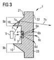
図3に示された実施例が図1に示された実施例と異なる点は、ベースボディ23が反射性部分領域9a,9bを有することである。たとえば反射性部分領域9a,9bは、第1の主表面21のところでキャビティ3から横方向に間隔をおいて配置されている。
The embodiment shown in FIG. 3 is different from the embodiment shown in FIG. 1 in that the
横方向の部分領域9a,9bは有利には、それらが光源5を囲む高さを有している。
The lateral
光源5から送出される放射を、素子の外観イメージ殊に放射特性がさらに改善されるよう、反射性部分領域9a,9bのところで反射させることができる。
The radiation emitted from the light source 5 can be reflected at the reflective
ここでも放射経路について想定される例が、矢印6,6a,6b,6c,6d,7,7a,7bによって描かれている。
Here again, examples of possible radiation paths are depicted by
一例として、光源5から送出される放射7は、反射性部分領域のうち一方の部分領域9aに入射し、この反射性部分領域9a内を放射7aとして案内されて、たとえば反射特性を有する主表面21に当射してこの面で反射し、その結果、この放射は第2の主表面22の方向へ案内されて、第2の主表面22のところで放射7bとしてレンズ1から出射する。したがって放射7は注封材料4を通っては案内されず、それゆえレンズ1内で散乱プロセスを受けない。
As an example, the radiation 7 emitted from the light source 5 is incident on one
これに対し、光源5から送出され注封材料4に入射する放射6は、反射性部分領域9a,9bのいずれも通過せず、図1の実施例の場合のようにディフューザのところで拡散性で散乱し、反射プロセスは受けない。
On the other hand, the
反射性部分領域9a,9bの反射特性を、たとえば第1の主表面21に設けられた反射層10によって実現することができる。択一的に、反射性部分領域9a,9bと周囲媒体との屈折率の差によって反射を実現することができる。
The reflection characteristics of the reflective
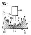
図4の実施例は、製造プロセスにおけるレンズ1の横断面を示すものである。たとえば図4の実施例のレンズはフレネルレンズの形式に従い形成されている。フレネルレンズはたとえば主表面のところに、この事例では第1の主表面21に、複数の段12a,12b,12cを有している。第2の主表面22も同じように形成することができる。
The embodiment of FIG. 4 shows a cross section of the
ベースボディ23のキャビティは、有利にはフレネルレンズの第1の段12aにより形成される。フレネルレンズの第1の段12aは、たとえばレンズの中央の段である。
The cavity of the
たとえば第1の段12aは高さHを有しており、この高さまで注封材料4によって充填される。
For example, the
択一的に、注封材料4の充填レベルを第1の段12aの高さHよりも低くしてもよい(図示せず)。このケースでは、注封材料4は第1の段12aの高さHを完全には充填しきらないので、放射をフレネル構造殊に第1の段12aの中に案内することができ、有利にはこのことは光学系の効率改善に寄与する。
Alternatively, the filling level of the
注封材料4は有利にはディスペンス技術によってキャビティ内に取り込まれる。この目的で、注封材料4がたとえばキャビティ3に滴加される。このような滴加は、たとえばスポイト11やピペット11などを用いて行うことができる。なお、ディスペンスステップにおける注封材料4の温度は、ベースボディ23の材料の溶融温度よりも低いと有利である。その後、注封材料4は冷却により硬化される。
The
さらに注封材料4をジェットプロセスによってキャビティ3内に取り込むこともできる(図示せず)。
Further, the
図5Aおよび図5Bには、それぞれベースボディ23と注封材料4を有するレンズ1が示されている。
5A and 5B show the
図1に示したレンズ1とは異なり、図5Aおよび図5Bの実施例によれば注封材料4はベースボディ23の第1の主表面21とは同一平面上で終端していない。殊に、注封材料4においてベースボディ23とは反対側の表面は湾曲している。さらにたとえば、注封材料4においてベースボディ23とは反対側の表面を、レンズ1の用途に応じて集光レンズまたは分散レンズないしは凹レンズの形式で構成することができる。
Unlike the
図5Aの実施例によれば、注封材料4においてベースボディ23とは反対側の表面は凹面の湾曲を有しているのに対し、図5Bに示したレンズ1の場合、注封材料4においてベースボディ23とは反対側の表面は凸面の湾曲を有している。
According to the embodiment of FIG. 5A, the surface of the
注封材料4においてベースボディ23とは反対側の表面が湾曲していることによりレンズ1のこの領域において、予め定められた殊に望ましい光の案内を実現することができる。殊に、たとえば部分的に放射を束ねたり放射を分散させたりすることができる。
The curved surface of the
これまで本発明について実施例に基づき説明してきたが、本発明は既述の実施例に限定されるものではなく、そのもの自体が実施例に基づき特許請求の範囲に明示的には記載されていないにしても、いかなる新たな特徴も、あるいはそれらの特徴のいかなる組み合わせも含むものである。 Although the present invention has been described based on the embodiments so far, the present invention is not limited to the above-described embodiments, and itself is not explicitly described in the claims based on the embodiments. Nevertheless, it includes any new features or any combination of these features.
Claims (15)
ベースボディ(23)と注封材料(4)が設けられており、
前記ベースボディ(23)は、第1の主表面(21)と、第2の主表面(22)と、前記第1の主表面(21)に配置された少なくとも1つのキャビティ(3)とを有しており、
前記注封材料(4)は、前記キャビティ(3)内に配置されていて、少なくとも1つのディフューザを有しており、該ディフューザは、少なくとも1つの波長領域の放射を散乱させることを特徴とするレンズ。 In lens (1):
A base body (23) and a potting material (4) are provided,
The base body (23) includes a first main surface (21), a second main surface (22), and at least one cavity (3) disposed on the first main surface (21). Have
The potting material (4) is arranged in the cavity (3) and has at least one diffuser, which diffuses radiation in at least one wavelength region. lens.
請求項1から10のいずれか1項記載の少なくとも1つのレンズ(1)と、
少なくとも1つの光源(5)が設けられており、
該光源(5)は、前記第1の主表面(21)の側に配置されていることを特徴とする、
オプトエレクトロニクス素子。 In optoelectronic devices,
At least one lens (1) according to any one of the preceding claims,
At least one light source (5) is provided,
The light source (5) is arranged on the first main surface (21) side,
Optoelectronic element.
前記注封材料(4)はディスペンス技術によって前記キャビティ(3)内に収容されることを特徴とする方法。 In the manufacturing method of the lens of any one of Claim 1 to 10,
Method according to claim 1, characterized in that the potting material (4) is accommodated in the cavity (3) by means of a dispensing technique.
Applications Claiming Priority (3)
| Application Number | Priority Date | Filing Date | Title |
|---|---|---|---|
| DE200910017946 DE102009017946A1 (en) | 2009-04-17 | 2009-04-17 | Lens, optoelectronic component having a lens and method for producing a lens |
| DE102009017946.1 | 2009-04-17 | ||
| PCT/DE2010/000251 WO2010118718A1 (en) | 2009-04-17 | 2010-03-05 | Lens, optoelectronic component comprising a lens, and method for producing a lens |
Publications (2)
| Publication Number | Publication Date |
|---|---|
| JP2012524287A true JP2012524287A (en) | 2012-10-11 |
| JP2012524287A5 JP2012524287A5 (en) | 2013-02-07 |
Family
ID=42224386
Family Applications (1)
| Application Number | Title | Priority Date | Filing Date |
|---|---|---|---|
| JP2012505043A Pending JP2012524287A (en) | 2009-04-17 | 2010-03-05 | Lens, optoelectronic element having lens, and method of manufacturing lens |
Country Status (8)
| Country | Link |
|---|---|
| US (1) | US8848297B2 (en) |
| EP (1) | EP2419779A1 (en) |
| JP (1) | JP2012524287A (en) |
| KR (1) | KR20120008057A (en) |
| CN (1) | CN102395913A (en) |
| DE (1) | DE102009017946A1 (en) |
| TW (1) | TWI426301B (en) |
| WO (1) | WO2010118718A1 (en) |
Cited By (1)
| Publication number | Priority date | Publication date | Assignee | Title |
|---|---|---|---|---|
| JP2015011799A (en) * | 2013-06-27 | 2015-01-19 | コニカミノルタ株式会社 | Light emitting unit and electronic apparatus |
Families Citing this family (12)
| Publication number | Priority date | Publication date | Assignee | Title |
|---|---|---|---|---|
| DE102009047788A1 (en) * | 2009-09-30 | 2011-03-31 | Osram Opto Semiconductors Gmbh | Lighting device for a camera and method for operating the same |
| JP5028569B2 (en) * | 2010-12-01 | 2012-09-19 | ナルックス株式会社 | Optical element |
| KR20120082655A (en) | 2011-01-14 | 2012-07-24 | 삼성전자주식회사 | Led flash lens unit and method for manufacturing same |
| US10047930B2 (en) * | 2011-12-02 | 2018-08-14 | Seoul Semiconductor Co., Ltd. | Light emitting module and lens |
| EP4242516A3 (en) | 2011-12-02 | 2023-11-22 | Seoul Semiconductor Co., Ltd. | Light emitting module and lens |
| JP2015535951A (en) * | 2012-09-19 | 2015-12-17 | ヴェンティス テクノロジーズ エルエルシー | Light scattering device |
| US10400984B2 (en) * | 2013-03-15 | 2019-09-03 | Cree, Inc. | LED light fixture and unitary optic member therefor |
| JP5403775B1 (en) * | 2013-03-27 | 2014-01-29 | 株式会社光波 | Lighting device and display device |
| CN104421834A (en) * | 2013-08-28 | 2015-03-18 | 鸿富锦精密工业(深圳)有限公司 | Compound lens and manufacturing method thereof and light source device using same |
| CN104864360B (en) * | 2015-05-27 | 2023-05-02 | 漳州立达信光电子科技有限公司 | Lens structure |
| DE102016218139A1 (en) | 2016-09-21 | 2018-04-05 | Osram Gmbh | lighting device |
| WO2019071085A1 (en) | 2017-10-06 | 2019-04-11 | Zodiac Pool Systems Llc | Lighting assemblies principally for swimming pools and spas |
Citations (4)
| Publication number | Priority date | Publication date | Assignee | Title |
|---|---|---|---|---|
| JPH0469809U (en) * | 1990-10-26 | 1992-06-19 | ||
| JP2003110146A (en) * | 2001-07-26 | 2003-04-11 | Matsushita Electric Works Ltd | Light-emitting device |
| JP2006519500A (en) * | 2003-02-26 | 2006-08-24 | クリー インコーポレイテッド | Synthetic white light source and manufacturing method thereof |
| JP2007005218A (en) * | 2005-06-27 | 2007-01-11 | Matsushita Electric Works Ltd | Light emitting apparatus and lighting equipment provided therewith |
Family Cites Families (28)
| Publication number | Priority date | Publication date | Assignee | Title |
|---|---|---|---|---|
| JPS48102585A (en) | 1972-04-04 | 1973-12-22 | ||
| US4603496A (en) | 1985-02-04 | 1986-08-05 | Adaptive Micro Systems, Inc. | Electronic display with lens matrix |
| US5140220A (en) | 1985-12-02 | 1992-08-18 | Yumi Sakai | Light diffusion type light emitting diode |
| US5001609A (en) | 1988-10-05 | 1991-03-19 | Hewlett-Packard Company | Nonimaging light source |
| AU2001245787A1 (en) * | 2000-03-17 | 2001-10-03 | Zograph, Llc | High acuity lens system |
| DE10051464B4 (en) | 2000-10-17 | 2011-08-11 | OSRAM Opto Semiconductors GmbH, 93055 | fresnel lens |
| US7055996B2 (en) | 2002-03-19 | 2006-06-06 | Truck-Lite Co., Inc. | Side turn/marker lamp |
| US6654174B1 (en) * | 2002-05-08 | 2003-11-25 | Pin Chien Huang | Micro lens systems and articles thereof |
| JP3707688B2 (en) * | 2002-05-31 | 2005-10-19 | スタンレー電気株式会社 | Light emitting device and manufacturing method thereof |
| KR100603535B1 (en) * | 2002-08-30 | 2006-07-24 | 다이니폰 인사츠 가부시키가이샤 | Lens sheet and rear projection screen including the same |
| US7233106B2 (en) | 2004-07-14 | 2007-06-19 | Taiwan Oasis Technology Co., Ltd. | LED chip capping construction |
| JPWO2006009193A1 (en) | 2004-07-23 | 2008-05-01 | 株式会社クラレ | Rear projection type screen and rear projection type projection device |
| DE102004042125B4 (en) * | 2004-08-30 | 2008-05-08 | Schefenacker Vision Systems Germany Gmbh & Co. Kg | Lighting unit with a large number of curved surface elements |
| KR100631992B1 (en) * | 2005-07-19 | 2006-10-09 | 삼성전기주식회사 | Light emitting diode package having dual lens structure for laterally emitting light |
| KR100611922B1 (en) | 2005-09-27 | 2006-08-11 | 엘지전자 주식회사 | Lens for use in light emitting device and package using the lens |
| KR20090005194A (en) * | 2006-04-18 | 2009-01-12 | 라미나 라이팅, 인크. | Optical devices for controlled color mixing |
| JP4952051B2 (en) * | 2006-05-10 | 2012-06-13 | ソニー株式会社 | METAL OXIDE NANOPARTICLE, ITS MANUFACTURING METHOD, LIGHT EMITTING ELEMENT ASSEMBLY AND OPTICAL MATERIAL |
| EP2056016B1 (en) | 2006-08-25 | 2014-08-20 | Furukawa Electric Co., Ltd. | Illumination device |
| US7719636B2 (en) * | 2007-03-14 | 2010-05-18 | Lg Electronics Inc. | Optical sheet and liquid crystal display using the same |
| TW200839378A (en) * | 2007-03-21 | 2008-10-01 | Chi Mei Optoelectronics Corp | Light emitting element, backlight module and plane display apparatus |
| EP2147250A1 (en) * | 2007-04-17 | 2010-01-27 | Philips Intellectual Property & Standards GmbH | Illumination device |
| US20090016051A1 (en) * | 2007-04-25 | 2009-01-15 | Bright View Technologies, Inc. | Light emitting device diffusers for general application lighting |
| US7999283B2 (en) | 2007-06-14 | 2011-08-16 | Cree, Inc. | Encapsulant with scatterer to tailor spatial emission pattern and color uniformity in light emitting diodes |
| GB0712614D0 (en) | 2007-06-29 | 2007-08-08 | Dialight Lumidrives Ltd | Improved spatial luminance |
| EP2188668A1 (en) * | 2007-08-27 | 2010-05-26 | Koninklijke Philips Electronics N.V. | Light output device |
| CN201152494Y (en) * | 2007-12-25 | 2008-11-19 | 欧创光电股份有限公司 | Light source lens structural improvement |
| DE102008025756B4 (en) * | 2008-05-29 | 2023-02-23 | OSRAM Opto Semiconductors Gesellschaft mit beschränkter Haftung | semiconductor device |
| US8313218B2 (en) * | 2009-05-25 | 2012-11-20 | Lg Innotek, Co., Ltd. | Gap member, lens and lighting device having the same |
-
2009
- 2009-04-17 DE DE200910017946 patent/DE102009017946A1/en not_active Withdrawn
-
2010
- 2010-03-05 KR KR1020117027409A patent/KR20120008057A/en not_active Application Discontinuation
- 2010-03-05 CN CN2010800169804A patent/CN102395913A/en active Pending
- 2010-03-05 US US13/263,104 patent/US8848297B2/en not_active Expired - Fee Related
- 2010-03-05 JP JP2012505043A patent/JP2012524287A/en active Pending
- 2010-03-05 WO PCT/DE2010/000251 patent/WO2010118718A1/en active Application Filing
- 2010-03-05 EP EP10716457A patent/EP2419779A1/en not_active Withdrawn
- 2010-03-22 TW TW099108275A patent/TWI426301B/en not_active IP Right Cessation
Patent Citations (4)
| Publication number | Priority date | Publication date | Assignee | Title |
|---|---|---|---|---|
| JPH0469809U (en) * | 1990-10-26 | 1992-06-19 | ||
| JP2003110146A (en) * | 2001-07-26 | 2003-04-11 | Matsushita Electric Works Ltd | Light-emitting device |
| JP2006519500A (en) * | 2003-02-26 | 2006-08-24 | クリー インコーポレイテッド | Synthetic white light source and manufacturing method thereof |
| JP2007005218A (en) * | 2005-06-27 | 2007-01-11 | Matsushita Electric Works Ltd | Light emitting apparatus and lighting equipment provided therewith |
Cited By (1)
| Publication number | Priority date | Publication date | Assignee | Title |
|---|---|---|---|---|
| JP2015011799A (en) * | 2013-06-27 | 2015-01-19 | コニカミノルタ株式会社 | Light emitting unit and electronic apparatus |
Also Published As
| Publication number | Publication date |
|---|---|
| TW201106018A (en) | 2011-02-16 |
| CN102395913A (en) | 2012-03-28 |
| KR20120008057A (en) | 2012-01-25 |
| WO2010118718A1 (en) | 2010-10-21 |
| EP2419779A1 (en) | 2012-02-22 |
| TWI426301B (en) | 2014-02-11 |
| US20120162783A1 (en) | 2012-06-28 |
| DE102009017946A1 (en) | 2010-10-21 |
| US8848297B2 (en) | 2014-09-30 |
Similar Documents
| Publication | Publication Date | Title |
|---|---|---|
| JP2012524287A (en) | Lens, optoelectronic element having lens, and method of manufacturing lens | |
| US8324797B2 (en) | White light emitting diode and method of manufacturing the same | |
| KR101835907B1 (en) | Optoelectronic component | |
| KR101892593B1 (en) | A light emitting device and the manufacturing method | |
| US6730940B1 (en) | Enhanced brightness light emitting device spot emitter | |
| JP5824142B2 (en) | Optical element, optoelectronic component, and manufacturing method thereof | |
| TWI507635B (en) | Led with molded bi-directional optics | |
| JP5566114B2 (en) | Optoelectronic device having a casing body and method of manufacturing the same | |
| KR102510808B1 (en) | Light source assembly with improved color uniformity | |
| US11598509B2 (en) | Backlight unit | |
| US8960932B2 (en) | Light emitting device | |
| CN102870239B (en) | Opto-electronic device and the method for the manufacture of opto-electronic device | |
| CN113238312A (en) | Display device | |
| KR20140053205A (en) | Optoelectronic component and method for producing an optoelectronic component | |
| US20080211388A1 (en) | Light emitting semiconductor device | |
| CN112531095A (en) | Backlight unit | |
| CN111512436A (en) | Optoelectronic component | |
| US20150162510A1 (en) | Light emitting diode module | |
| KR102519814B1 (en) | LED module with high near-field contrast ratio | |
| KR20130074326A (en) | Manufacturing method of light emitting device having wavelenth-converting layer and light emitting device produced by the same | |
| KR20070079235A (en) | Light emitting diode package | |
| JP7285439B2 (en) | planar light source | |
| KR20080032318A (en) | Light emitting device |
Legal Events
| Date | Code | Title | Description |
|---|---|---|---|
| A521 | Request for written amendment filed |
Free format text: JAPANESE INTERMEDIATE CODE: A523 Effective date: 20121213 |
|
| A621 | Written request for application examination |
Free format text: JAPANESE INTERMEDIATE CODE: A621 Effective date: 20121213 |
|
| A977 | Report on retrieval |
Free format text: JAPANESE INTERMEDIATE CODE: A971007 Effective date: 20131225 |
|
| A131 | Notification of reasons for refusal |
Free format text: JAPANESE INTERMEDIATE CODE: A131 Effective date: 20140106 |
|
| A02 | Decision of refusal |
Free format text: JAPANESE INTERMEDIATE CODE: A02 Effective date: 20140609 |