JP2012519374A - Semiconductor device metallization system including metal pillars with decreasing diameter at the bottom - Google Patents
Semiconductor device metallization system including metal pillars with decreasing diameter at the bottom Download PDFInfo
- Publication number
- JP2012519374A JP2012519374A JP2011551432A JP2011551432A JP2012519374A JP 2012519374 A JP2012519374 A JP 2012519374A JP 2011551432 A JP2011551432 A JP 2011551432A JP 2011551432 A JP2011551432 A JP 2011551432A JP 2012519374 A JP2012519374 A JP 2012519374A
- Authority
- JP
- Japan
- Prior art keywords
- passivation layer
- opening
- semiconductor device
- lateral dimension
- metal pillar
- Prior art date
- Legal status (The legal status is an assumption and is not a legal conclusion. Google has not performed a legal analysis and makes no representation as to the accuracy of the status listed.)
- Pending
Links
Images


Classifications
-
- H—ELECTRICITY
- H01—ELECTRIC ELEMENTS
- H01L—SEMICONDUCTOR DEVICES NOT COVERED BY CLASS H10
- H01L24/00—Arrangements for connecting or disconnecting semiconductor or solid-state bodies; Methods or apparatus related thereto
- H01L24/01—Means for bonding being attached to, or being formed on, the surface to be connected, e.g. chip-to-package, die-attach, "first-level" interconnects; Manufacturing methods related thereto
- H01L24/02—Bonding areas ; Manufacturing methods related thereto
- H01L24/03—Manufacturing methods
-
- H—ELECTRICITY
- H01—ELECTRIC ELEMENTS
- H01L—SEMICONDUCTOR DEVICES NOT COVERED BY CLASS H10
- H01L23/00—Details of semiconductor or other solid state devices
- H01L23/48—Arrangements for conducting electric current to or from the solid state body in operation, e.g. leads, terminal arrangements ; Selection of materials therefor
- H01L23/482—Arrangements for conducting electric current to or from the solid state body in operation, e.g. leads, terminal arrangements ; Selection of materials therefor consisting of lead-in layers inseparably applied to the semiconductor body
- H01L23/485—Arrangements for conducting electric current to or from the solid state body in operation, e.g. leads, terminal arrangements ; Selection of materials therefor consisting of lead-in layers inseparably applied to the semiconductor body consisting of layered constructions comprising conductive layers and insulating layers, e.g. planar contacts
-
- H—ELECTRICITY
- H01—ELECTRIC ELEMENTS
- H01L—SEMICONDUCTOR DEVICES NOT COVERED BY CLASS H10
- H01L24/00—Arrangements for connecting or disconnecting semiconductor or solid-state bodies; Methods or apparatus related thereto
- H01L24/01—Means for bonding being attached to, or being formed on, the surface to be connected, e.g. chip-to-package, die-attach, "first-level" interconnects; Manufacturing methods related thereto
- H01L24/02—Bonding areas ; Manufacturing methods related thereto
- H01L24/04—Structure, shape, material or disposition of the bonding areas prior to the connecting process
- H01L24/05—Structure, shape, material or disposition of the bonding areas prior to the connecting process of an individual bonding area
-
- H—ELECTRICITY
- H01—ELECTRIC ELEMENTS
- H01L—SEMICONDUCTOR DEVICES NOT COVERED BY CLASS H10
- H01L24/00—Arrangements for connecting or disconnecting semiconductor or solid-state bodies; Methods or apparatus related thereto
- H01L24/01—Means for bonding being attached to, or being formed on, the surface to be connected, e.g. chip-to-package, die-attach, "first-level" interconnects; Manufacturing methods related thereto
- H01L24/10—Bump connectors ; Manufacturing methods related thereto
- H01L24/11—Manufacturing methods
-
- H—ELECTRICITY
- H01—ELECTRIC ELEMENTS
- H01L—SEMICONDUCTOR DEVICES NOT COVERED BY CLASS H10
- H01L24/00—Arrangements for connecting or disconnecting semiconductor or solid-state bodies; Methods or apparatus related thereto
- H01L24/01—Means for bonding being attached to, or being formed on, the surface to be connected, e.g. chip-to-package, die-attach, "first-level" interconnects; Manufacturing methods related thereto
- H01L24/10—Bump connectors ; Manufacturing methods related thereto
- H01L24/12—Structure, shape, material or disposition of the bump connectors prior to the connecting process
-
- H—ELECTRICITY
- H01—ELECTRIC ELEMENTS
- H01L—SEMICONDUCTOR DEVICES NOT COVERED BY CLASS H10
- H01L2224/00—Indexing scheme for arrangements for connecting or disconnecting semiconductor or solid-state bodies and methods related thereto as covered by H01L24/00
- H01L2224/01—Means for bonding being attached to, or being formed on, the surface to be connected, e.g. chip-to-package, die-attach, "first-level" interconnects; Manufacturing methods related thereto
- H01L2224/02—Bonding areas; Manufacturing methods related thereto
- H01L2224/04—Structure, shape, material or disposition of the bonding areas prior to the connecting process
- H01L2224/0401—Bonding areas specifically adapted for bump connectors, e.g. under bump metallisation [UBM]
-
- H—ELECTRICITY
- H01—ELECTRIC ELEMENTS
- H01L—SEMICONDUCTOR DEVICES NOT COVERED BY CLASS H10
- H01L2224/00—Indexing scheme for arrangements for connecting or disconnecting semiconductor or solid-state bodies and methods related thereto as covered by H01L24/00
- H01L2224/01—Means for bonding being attached to, or being formed on, the surface to be connected, e.g. chip-to-package, die-attach, "first-level" interconnects; Manufacturing methods related thereto
- H01L2224/02—Bonding areas; Manufacturing methods related thereto
- H01L2224/04—Structure, shape, material or disposition of the bonding areas prior to the connecting process
- H01L2224/05—Structure, shape, material or disposition of the bonding areas prior to the connecting process of an individual bonding area
- H01L2224/05001—Internal layers
- H01L2224/05075—Plural internal layers
- H01L2224/0508—Plural internal layers being stacked
- H01L2224/05082—Two-layer arrangements
-
- H—ELECTRICITY
- H01—ELECTRIC ELEMENTS
- H01L—SEMICONDUCTOR DEVICES NOT COVERED BY CLASS H10
- H01L2224/00—Indexing scheme for arrangements for connecting or disconnecting semiconductor or solid-state bodies and methods related thereto as covered by H01L24/00
- H01L2224/01—Means for bonding being attached to, or being formed on, the surface to be connected, e.g. chip-to-package, die-attach, "first-level" interconnects; Manufacturing methods related thereto
- H01L2224/02—Bonding areas; Manufacturing methods related thereto
- H01L2224/04—Structure, shape, material or disposition of the bonding areas prior to the connecting process
- H01L2224/05—Structure, shape, material or disposition of the bonding areas prior to the connecting process of an individual bonding area
- H01L2224/05001—Internal layers
- H01L2224/05075—Plural internal layers
- H01L2224/0508—Plural internal layers being stacked
- H01L2224/05085—Plural internal layers being stacked with additional elements, e.g. vias arrays, interposed between the stacked layers
- H01L2224/05089—Disposition of the additional element
- H01L2224/05093—Disposition of the additional element of a plurality of vias
- H01L2224/05096—Uniform arrangement, i.e. array
-
- H—ELECTRICITY
- H01—ELECTRIC ELEMENTS
- H01L—SEMICONDUCTOR DEVICES NOT COVERED BY CLASS H10
- H01L2224/00—Indexing scheme for arrangements for connecting or disconnecting semiconductor or solid-state bodies and methods related thereto as covered by H01L24/00
- H01L2224/01—Means for bonding being attached to, or being formed on, the surface to be connected, e.g. chip-to-package, die-attach, "first-level" interconnects; Manufacturing methods related thereto
- H01L2224/02—Bonding areas; Manufacturing methods related thereto
- H01L2224/04—Structure, shape, material or disposition of the bonding areas prior to the connecting process
- H01L2224/05—Structure, shape, material or disposition of the bonding areas prior to the connecting process of an individual bonding area
- H01L2224/0554—External layer
- H01L2224/05599—Material
- H01L2224/056—Material with a principal constituent of the material being a metal or a metalloid, e.g. boron [B], silicon [Si], germanium [Ge], arsenic [As], antimony [Sb], tellurium [Te] and polonium [Po], and alloys thereof
- H01L2224/05617—Material with a principal constituent of the material being a metal or a metalloid, e.g. boron [B], silicon [Si], germanium [Ge], arsenic [As], antimony [Sb], tellurium [Te] and polonium [Po], and alloys thereof the principal constituent melting at a temperature of greater than or equal to 400°C and less than 950°C
- H01L2224/05624—Aluminium [Al] as principal constituent
-
- H—ELECTRICITY
- H01—ELECTRIC ELEMENTS
- H01L—SEMICONDUCTOR DEVICES NOT COVERED BY CLASS H10
- H01L2224/00—Indexing scheme for arrangements for connecting or disconnecting semiconductor or solid-state bodies and methods related thereto as covered by H01L24/00
- H01L2224/01—Means for bonding being attached to, or being formed on, the surface to be connected, e.g. chip-to-package, die-attach, "first-level" interconnects; Manufacturing methods related thereto
- H01L2224/02—Bonding areas; Manufacturing methods related thereto
- H01L2224/04—Structure, shape, material or disposition of the bonding areas prior to the connecting process
- H01L2224/05—Structure, shape, material or disposition of the bonding areas prior to the connecting process of an individual bonding area
- H01L2224/0554—External layer
- H01L2224/05599—Material
- H01L2224/056—Material with a principal constituent of the material being a metal or a metalloid, e.g. boron [B], silicon [Si], germanium [Ge], arsenic [As], antimony [Sb], tellurium [Te] and polonium [Po], and alloys thereof
- H01L2224/05638—Material with a principal constituent of the material being a metal or a metalloid, e.g. boron [B], silicon [Si], germanium [Ge], arsenic [As], antimony [Sb], tellurium [Te] and polonium [Po], and alloys thereof the principal constituent melting at a temperature of greater than or equal to 950°C and less than 1550°C
- H01L2224/05647—Copper [Cu] as principal constituent
-
- H—ELECTRICITY
- H01—ELECTRIC ELEMENTS
- H01L—SEMICONDUCTOR DEVICES NOT COVERED BY CLASS H10
- H01L2224/00—Indexing scheme for arrangements for connecting or disconnecting semiconductor or solid-state bodies and methods related thereto as covered by H01L24/00
- H01L2224/01—Means for bonding being attached to, or being formed on, the surface to be connected, e.g. chip-to-package, die-attach, "first-level" interconnects; Manufacturing methods related thereto
- H01L2224/10—Bump connectors; Manufacturing methods related thereto
- H01L2224/11—Manufacturing methods
- H01L2224/114—Manufacturing methods by blanket deposition of the material of the bump connector
- H01L2224/1146—Plating
- H01L2224/11462—Electroplating
-
- H—ELECTRICITY
- H01—ELECTRIC ELEMENTS
- H01L—SEMICONDUCTOR DEVICES NOT COVERED BY CLASS H10
- H01L2224/00—Indexing scheme for arrangements for connecting or disconnecting semiconductor or solid-state bodies and methods related thereto as covered by H01L24/00
- H01L2224/01—Means for bonding being attached to, or being formed on, the surface to be connected, e.g. chip-to-package, die-attach, "first-level" interconnects; Manufacturing methods related thereto
- H01L2224/10—Bump connectors; Manufacturing methods related thereto
- H01L2224/11—Manufacturing methods
- H01L2224/114—Manufacturing methods by blanket deposition of the material of the bump connector
- H01L2224/1146—Plating
- H01L2224/11464—Electroless plating
-
- H—ELECTRICITY
- H01—ELECTRIC ELEMENTS
- H01L—SEMICONDUCTOR DEVICES NOT COVERED BY CLASS H10
- H01L2224/00—Indexing scheme for arrangements for connecting or disconnecting semiconductor or solid-state bodies and methods related thereto as covered by H01L24/00
- H01L2224/01—Means for bonding being attached to, or being formed on, the surface to be connected, e.g. chip-to-package, die-attach, "first-level" interconnects; Manufacturing methods related thereto
- H01L2224/10—Bump connectors; Manufacturing methods related thereto
- H01L2224/11—Manufacturing methods
- H01L2224/1147—Manufacturing methods using a lift-off mask
- H01L2224/11472—Profile of the lift-off mask
-
- H—ELECTRICITY
- H01—ELECTRIC ELEMENTS
- H01L—SEMICONDUCTOR DEVICES NOT COVERED BY CLASS H10
- H01L2224/00—Indexing scheme for arrangements for connecting or disconnecting semiconductor or solid-state bodies and methods related thereto as covered by H01L24/00
- H01L2224/01—Means for bonding being attached to, or being formed on, the surface to be connected, e.g. chip-to-package, die-attach, "first-level" interconnects; Manufacturing methods related thereto
- H01L2224/10—Bump connectors; Manufacturing methods related thereto
- H01L2224/11—Manufacturing methods
- H01L2224/1147—Manufacturing methods using a lift-off mask
- H01L2224/11474—Multilayer masks
-
- H—ELECTRICITY
- H01—ELECTRIC ELEMENTS
- H01L—SEMICONDUCTOR DEVICES NOT COVERED BY CLASS H10
- H01L2224/00—Indexing scheme for arrangements for connecting or disconnecting semiconductor or solid-state bodies and methods related thereto as covered by H01L24/00
- H01L2224/01—Means for bonding being attached to, or being formed on, the surface to be connected, e.g. chip-to-package, die-attach, "first-level" interconnects; Manufacturing methods related thereto
- H01L2224/10—Bump connectors; Manufacturing methods related thereto
- H01L2224/11—Manufacturing methods
- H01L2224/118—Post-treatment of the bump connector
- H01L2224/11848—Thermal treatments, e.g. annealing, controlled cooling
- H01L2224/11849—Reflowing
-
- H—ELECTRICITY
- H01—ELECTRIC ELEMENTS
- H01L—SEMICONDUCTOR DEVICES NOT COVERED BY CLASS H10
- H01L2224/00—Indexing scheme for arrangements for connecting or disconnecting semiconductor or solid-state bodies and methods related thereto as covered by H01L24/00
- H01L2224/01—Means for bonding being attached to, or being formed on, the surface to be connected, e.g. chip-to-package, die-attach, "first-level" interconnects; Manufacturing methods related thereto
- H01L2224/10—Bump connectors; Manufacturing methods related thereto
- H01L2224/11—Manufacturing methods
- H01L2224/119—Methods of manufacturing bump connectors involving a specific sequence of method steps
- H01L2224/11901—Methods of manufacturing bump connectors involving a specific sequence of method steps with repetition of the same manufacturing step
-
- H—ELECTRICITY
- H01—ELECTRIC ELEMENTS
- H01L—SEMICONDUCTOR DEVICES NOT COVERED BY CLASS H10
- H01L2224/00—Indexing scheme for arrangements for connecting or disconnecting semiconductor or solid-state bodies and methods related thereto as covered by H01L24/00
- H01L2224/01—Means for bonding being attached to, or being formed on, the surface to be connected, e.g. chip-to-package, die-attach, "first-level" interconnects; Manufacturing methods related thereto
- H01L2224/10—Bump connectors; Manufacturing methods related thereto
- H01L2224/12—Structure, shape, material or disposition of the bump connectors prior to the connecting process
- H01L2224/13—Structure, shape, material or disposition of the bump connectors prior to the connecting process of an individual bump connector
- H01L2224/13001—Core members of the bump connector
- H01L2224/13005—Structure
- H01L2224/13006—Bump connector larger than the underlying bonding area, e.g. than the under bump metallisation [UBM]
-
- H—ELECTRICITY
- H01—ELECTRIC ELEMENTS
- H01L—SEMICONDUCTOR DEVICES NOT COVERED BY CLASS H10
- H01L2224/00—Indexing scheme for arrangements for connecting or disconnecting semiconductor or solid-state bodies and methods related thereto as covered by H01L24/00
- H01L2224/01—Means for bonding being attached to, or being formed on, the surface to be connected, e.g. chip-to-package, die-attach, "first-level" interconnects; Manufacturing methods related thereto
- H01L2224/10—Bump connectors; Manufacturing methods related thereto
- H01L2224/12—Structure, shape, material or disposition of the bump connectors prior to the connecting process
- H01L2224/13—Structure, shape, material or disposition of the bump connectors prior to the connecting process of an individual bump connector
- H01L2224/13001—Core members of the bump connector
- H01L2224/1301—Shape
- H01L2224/13016—Shape in side view
- H01L2224/13017—Shape in side view being non uniform along the bump connector
-
- H—ELECTRICITY
- H01—ELECTRIC ELEMENTS
- H01L—SEMICONDUCTOR DEVICES NOT COVERED BY CLASS H10
- H01L2224/00—Indexing scheme for arrangements for connecting or disconnecting semiconductor or solid-state bodies and methods related thereto as covered by H01L24/00
- H01L2224/01—Means for bonding being attached to, or being formed on, the surface to be connected, e.g. chip-to-package, die-attach, "first-level" interconnects; Manufacturing methods related thereto
- H01L2224/10—Bump connectors; Manufacturing methods related thereto
- H01L2224/12—Structure, shape, material or disposition of the bump connectors prior to the connecting process
- H01L2224/13—Structure, shape, material or disposition of the bump connectors prior to the connecting process of an individual bump connector
- H01L2224/13001—Core members of the bump connector
- H01L2224/1302—Disposition
- H01L2224/13022—Disposition the bump connector being at least partially embedded in the surface
-
- H—ELECTRICITY
- H01—ELECTRIC ELEMENTS
- H01L—SEMICONDUCTOR DEVICES NOT COVERED BY CLASS H10
- H01L2224/00—Indexing scheme for arrangements for connecting or disconnecting semiconductor or solid-state bodies and methods related thereto as covered by H01L24/00
- H01L2224/01—Means for bonding being attached to, or being formed on, the surface to be connected, e.g. chip-to-package, die-attach, "first-level" interconnects; Manufacturing methods related thereto
- H01L2224/10—Bump connectors; Manufacturing methods related thereto
- H01L2224/12—Structure, shape, material or disposition of the bump connectors prior to the connecting process
- H01L2224/13—Structure, shape, material or disposition of the bump connectors prior to the connecting process of an individual bump connector
- H01L2224/13001—Core members of the bump connector
- H01L2224/13075—Plural core members
- H01L2224/1308—Plural core members being stacked
- H01L2224/13082—Two-layer arrangements
-
- H—ELECTRICITY
- H01—ELECTRIC ELEMENTS
- H01L—SEMICONDUCTOR DEVICES NOT COVERED BY CLASS H10
- H01L2224/00—Indexing scheme for arrangements for connecting or disconnecting semiconductor or solid-state bodies and methods related thereto as covered by H01L24/00
- H01L2224/01—Means for bonding being attached to, or being formed on, the surface to be connected, e.g. chip-to-package, die-attach, "first-level" interconnects; Manufacturing methods related thereto
- H01L2224/10—Bump connectors; Manufacturing methods related thereto
- H01L2224/12—Structure, shape, material or disposition of the bump connectors prior to the connecting process
- H01L2224/13—Structure, shape, material or disposition of the bump connectors prior to the connecting process of an individual bump connector
- H01L2224/13001—Core members of the bump connector
- H01L2224/13099—Material
- H01L2224/131—Material with a principal constituent of the material being a metal or a metalloid, e.g. boron [B], silicon [Si], germanium [Ge], arsenic [As], antimony [Sb], tellurium [Te] and polonium [Po], and alloys thereof
- H01L2224/13138—Material with a principal constituent of the material being a metal or a metalloid, e.g. boron [B], silicon [Si], germanium [Ge], arsenic [As], antimony [Sb], tellurium [Te] and polonium [Po], and alloys thereof the principal constituent melting at a temperature of greater than or equal to 950°C and less than 1550°C
- H01L2224/13147—Copper [Cu] as principal constituent
-
- H—ELECTRICITY
- H01—ELECTRIC ELEMENTS
- H01L—SEMICONDUCTOR DEVICES NOT COVERED BY CLASS H10
- H01L2924/00—Indexing scheme for arrangements or methods for connecting or disconnecting semiconductor or solid-state bodies as covered by H01L24/00
- H01L2924/0001—Technical content checked by a classifier
- H01L2924/00013—Fully indexed content
-
- H—ELECTRICITY
- H01—ELECTRIC ELEMENTS
- H01L—SEMICONDUCTOR DEVICES NOT COVERED BY CLASS H10
- H01L2924/00—Indexing scheme for arrangements or methods for connecting or disconnecting semiconductor or solid-state bodies as covered by H01L24/00
- H01L2924/01—Chemical elements
- H01L2924/01005—Boron [B]
-
- H—ELECTRICITY
- H01—ELECTRIC ELEMENTS
- H01L—SEMICONDUCTOR DEVICES NOT COVERED BY CLASS H10
- H01L2924/00—Indexing scheme for arrangements or methods for connecting or disconnecting semiconductor or solid-state bodies as covered by H01L24/00
- H01L2924/01—Chemical elements
- H01L2924/01013—Aluminum [Al]
-
- H—ELECTRICITY
- H01—ELECTRIC ELEMENTS
- H01L—SEMICONDUCTOR DEVICES NOT COVERED BY CLASS H10
- H01L2924/00—Indexing scheme for arrangements or methods for connecting or disconnecting semiconductor or solid-state bodies as covered by H01L24/00
- H01L2924/01—Chemical elements
- H01L2924/01014—Silicon [Si]
-
- H—ELECTRICITY
- H01—ELECTRIC ELEMENTS
- H01L—SEMICONDUCTOR DEVICES NOT COVERED BY CLASS H10
- H01L2924/00—Indexing scheme for arrangements or methods for connecting or disconnecting semiconductor or solid-state bodies as covered by H01L24/00
- H01L2924/01—Chemical elements
- H01L2924/01019—Potassium [K]
-
- H—ELECTRICITY
- H01—ELECTRIC ELEMENTS
- H01L—SEMICONDUCTOR DEVICES NOT COVERED BY CLASS H10
- H01L2924/00—Indexing scheme for arrangements or methods for connecting or disconnecting semiconductor or solid-state bodies as covered by H01L24/00
- H01L2924/01—Chemical elements
- H01L2924/01024—Chromium [Cr]
-
- H—ELECTRICITY
- H01—ELECTRIC ELEMENTS
- H01L—SEMICONDUCTOR DEVICES NOT COVERED BY CLASS H10
- H01L2924/00—Indexing scheme for arrangements or methods for connecting or disconnecting semiconductor or solid-state bodies as covered by H01L24/00
- H01L2924/01—Chemical elements
- H01L2924/01028—Nickel [Ni]
-
- H—ELECTRICITY
- H01—ELECTRIC ELEMENTS
- H01L—SEMICONDUCTOR DEVICES NOT COVERED BY CLASS H10
- H01L2924/00—Indexing scheme for arrangements or methods for connecting or disconnecting semiconductor or solid-state bodies as covered by H01L24/00
- H01L2924/01—Chemical elements
- H01L2924/01029—Copper [Cu]
-
- H—ELECTRICITY
- H01—ELECTRIC ELEMENTS
- H01L—SEMICONDUCTOR DEVICES NOT COVERED BY CLASS H10
- H01L2924/00—Indexing scheme for arrangements or methods for connecting or disconnecting semiconductor or solid-state bodies as covered by H01L24/00
- H01L2924/01—Chemical elements
- H01L2924/01032—Germanium [Ge]
-
- H—ELECTRICITY
- H01—ELECTRIC ELEMENTS
- H01L—SEMICONDUCTOR DEVICES NOT COVERED BY CLASS H10
- H01L2924/00—Indexing scheme for arrangements or methods for connecting or disconnecting semiconductor or solid-state bodies as covered by H01L24/00
- H01L2924/01—Chemical elements
- H01L2924/01033—Arsenic [As]
-
- H—ELECTRICITY
- H01—ELECTRIC ELEMENTS
- H01L—SEMICONDUCTOR DEVICES NOT COVERED BY CLASS H10
- H01L2924/00—Indexing scheme for arrangements or methods for connecting or disconnecting semiconductor or solid-state bodies as covered by H01L24/00
- H01L2924/01—Chemical elements
- H01L2924/01047—Silver [Ag]
-
- H—ELECTRICITY
- H01—ELECTRIC ELEMENTS
- H01L—SEMICONDUCTOR DEVICES NOT COVERED BY CLASS H10
- H01L2924/00—Indexing scheme for arrangements or methods for connecting or disconnecting semiconductor or solid-state bodies as covered by H01L24/00
- H01L2924/01—Chemical elements
- H01L2924/01057—Lanthanum [La]
-
- H—ELECTRICITY
- H01—ELECTRIC ELEMENTS
- H01L—SEMICONDUCTOR DEVICES NOT COVERED BY CLASS H10
- H01L2924/00—Indexing scheme for arrangements or methods for connecting or disconnecting semiconductor or solid-state bodies as covered by H01L24/00
- H01L2924/01—Chemical elements
- H01L2924/01068—Erbium [Er]
-
- H—ELECTRICITY
- H01—ELECTRIC ELEMENTS
- H01L—SEMICONDUCTOR DEVICES NOT COVERED BY CLASS H10
- H01L2924/00—Indexing scheme for arrangements or methods for connecting or disconnecting semiconductor or solid-state bodies as covered by H01L24/00
- H01L2924/01—Chemical elements
- H01L2924/01073—Tantalum [Ta]
-
- H—ELECTRICITY
- H01—ELECTRIC ELEMENTS
- H01L—SEMICONDUCTOR DEVICES NOT COVERED BY CLASS H10
- H01L2924/00—Indexing scheme for arrangements or methods for connecting or disconnecting semiconductor or solid-state bodies as covered by H01L24/00
- H01L2924/01—Chemical elements
- H01L2924/01078—Platinum [Pt]
-
- H—ELECTRICITY
- H01—ELECTRIC ELEMENTS
- H01L—SEMICONDUCTOR DEVICES NOT COVERED BY CLASS H10
- H01L2924/00—Indexing scheme for arrangements or methods for connecting or disconnecting semiconductor or solid-state bodies as covered by H01L24/00
- H01L2924/01—Chemical elements
- H01L2924/01082—Lead [Pb]
-
- H—ELECTRICITY
- H01—ELECTRIC ELEMENTS
- H01L—SEMICONDUCTOR DEVICES NOT COVERED BY CLASS H10
- H01L2924/00—Indexing scheme for arrangements or methods for connecting or disconnecting semiconductor or solid-state bodies as covered by H01L24/00
- H01L2924/013—Alloys
- H01L2924/014—Solder alloys
-
- H—ELECTRICITY
- H01—ELECTRIC ELEMENTS
- H01L—SEMICONDUCTOR DEVICES NOT COVERED BY CLASS H10
- H01L2924/00—Indexing scheme for arrangements or methods for connecting or disconnecting semiconductor or solid-state bodies as covered by H01L24/00
- H01L2924/049—Nitrides composed of metals from groups of the periodic table
- H01L2924/0495—5th Group
- H01L2924/04953—TaN
-
- H—ELECTRICITY
- H01—ELECTRIC ELEMENTS
- H01L—SEMICONDUCTOR DEVICES NOT COVERED BY CLASS H10
- H01L2924/00—Indexing scheme for arrangements or methods for connecting or disconnecting semiconductor or solid-state bodies as covered by H01L24/00
- H01L2924/049—Nitrides composed of metals from groups of the periodic table
- H01L2924/0504—14th Group
- H01L2924/05042—Si3N4
-
- H—ELECTRICITY
- H01—ELECTRIC ELEMENTS
- H01L—SEMICONDUCTOR DEVICES NOT COVERED BY CLASS H10
- H01L2924/00—Indexing scheme for arrangements or methods for connecting or disconnecting semiconductor or solid-state bodies as covered by H01L24/00
- H01L2924/10—Details of semiconductor or other solid state devices to be connected
- H01L2924/102—Material of the semiconductor or solid state bodies
- H01L2924/1025—Semiconducting materials
- H01L2924/10251—Elemental semiconductors, i.e. Group IV
- H01L2924/10253—Silicon [Si]
-
- H—ELECTRICITY
- H01—ELECTRIC ELEMENTS
- H01L—SEMICONDUCTOR DEVICES NOT COVERED BY CLASS H10
- H01L2924/00—Indexing scheme for arrangements or methods for connecting or disconnecting semiconductor or solid-state bodies as covered by H01L24/00
- H01L2924/10—Details of semiconductor or other solid state devices to be connected
- H01L2924/11—Device type
- H01L2924/13—Discrete devices, e.g. 3 terminal devices
- H01L2924/1304—Transistor
- H01L2924/1306—Field-effect transistor [FET]
-
- H—ELECTRICITY
- H01—ELECTRIC ELEMENTS
- H01L—SEMICONDUCTOR DEVICES NOT COVERED BY CLASS H10
- H01L2924/00—Indexing scheme for arrangements or methods for connecting or disconnecting semiconductor or solid-state bodies as covered by H01L24/00
- H01L2924/10—Details of semiconductor or other solid state devices to be connected
- H01L2924/11—Device type
- H01L2924/14—Integrated circuits
- H01L2924/143—Digital devices
- H01L2924/1433—Application-specific integrated circuit [ASIC]
-
- H—ELECTRICITY
- H01—ELECTRIC ELEMENTS
- H01L—SEMICONDUCTOR DEVICES NOT COVERED BY CLASS H10
- H01L2924/00—Indexing scheme for arrangements or methods for connecting or disconnecting semiconductor or solid-state bodies as covered by H01L24/00
- H01L2924/19—Details of hybrid assemblies other than the semiconductor or other solid state devices to be connected
- H01L2924/1901—Structure
- H01L2924/1904—Component type
- H01L2924/19041—Component type being a capacitor
-
- H—ELECTRICITY
- H01—ELECTRIC ELEMENTS
- H01L—SEMICONDUCTOR DEVICES NOT COVERED BY CLASS H10
- H01L2924/00—Indexing scheme for arrangements or methods for connecting or disconnecting semiconductor or solid-state bodies as covered by H01L24/00
- H01L2924/19—Details of hybrid assemblies other than the semiconductor or other solid state devices to be connected
- H01L2924/1901—Structure
- H01L2924/1904—Component type
- H01L2924/19043—Component type being a resistor
-
- H—ELECTRICITY
- H01—ELECTRIC ELEMENTS
- H01L—SEMICONDUCTOR DEVICES NOT COVERED BY CLASS H10
- H01L2924/00—Indexing scheme for arrangements or methods for connecting or disconnecting semiconductor or solid-state bodies as covered by H01L24/00
- H01L2924/30—Technical effects
- H01L2924/301—Electrical effects
- H01L2924/30105—Capacitance
-
- H—ELECTRICITY
- H01—ELECTRIC ELEMENTS
- H01L—SEMICONDUCTOR DEVICES NOT COVERED BY CLASS H10
- H01L2924/00—Indexing scheme for arrangements or methods for connecting or disconnecting semiconductor or solid-state bodies as covered by H01L24/00
- H01L2924/30—Technical effects
- H01L2924/301—Electrical effects
- H01L2924/3025—Electromagnetic shielding
-
- H—ELECTRICITY
- H01—ELECTRIC ELEMENTS
- H01L—SEMICONDUCTOR DEVICES NOT COVERED BY CLASS H10
- H01L2924/00—Indexing scheme for arrangements or methods for connecting or disconnecting semiconductor or solid-state bodies as covered by H01L24/00
- H01L2924/30—Technical effects
- H01L2924/35—Mechanical effects
- H01L2924/351—Thermal stress
Abstract
【解決手段】
複雑な半導体デバイスのメタライゼーションシステムにおいて、メタライゼーションシステムに作用する最大の機械的応力を低減する一方で、パッケージ基板に接続するために必要とされるコンタクト表面を提供するために、銅ピラーのような金属ピラー(271)がくぎ状構造で形成されてよい。くぎ状構造は適切に構成されるレジストマスクに基いて得ることができる。
【選択図】図2e[Solution]
In complex semiconductor device metallization systems, such as copper pillars, to provide the contact surface required to connect to the package substrate while reducing the maximum mechanical stress acting on the metallization system. Metal pillars (271) may be formed with a nail-like structure. Nail-like structures can be obtained based on appropriately configured resist masks.
[Selection] Figure 2e
Description
概して本開示は、金属ピラーを含むメタライゼーションシステムを有する集積回路に関し、更に特定的にはチップとパッケージの間での熱的不整合に起因するチップ・パッケージ相互作用を低減するための技術に関する。 In general, this disclosure relates to integrated circuits having metallization systems including metal pillars, and more particularly to techniques for reducing chip-package interaction due to thermal mismatch between the chip and the package.
半導体デバイスは典型的には、任意の適切な材質から作製される実質的にディスク形状の基板上に形成される。高度に複雑な電子回路を含む半導体デバイスの大半は、現在のところシリコンに基いて製造されており、また当面の間シリコンに基いて製造されることが予測され、シリコン基板及び、SOI(シリコン・オン・インシュレータ)基板のようなシリコン含有基板は、マイクロプロセッサ、SRAM、ASIC(特定用途向けIC)、システム・オン・チップ(SoC)等の半導体デバイスを形成するための存続可能な基本的材質として提供されるであろう。個々の集積回路はウエハ上にアレイ状に配列されており、高度な集積回路における数百以上の個別プロセスステップを伴うであろう製造ステップの多くは、フォトリソグラフィプロセス、計測プロセス、及び基板をダイシングした後の個々のデバイスのパッケージングを除いて、基板上の全てのチップ区域に対して同時に実行される。従って、経済的な制約により、半導体製造業者は着実に基板寸法を大きくして、それにより実際の半導体デバイスの製造に利用可能な面積を増大するとともに製造歩留まりを高めることとなる。 The semiconductor device is typically formed on a substantially disk-shaped substrate made from any suitable material. The majority of semiconductor devices, including highly complex electronic circuits, are currently manufactured based on silicon and are expected to be based on silicon for the time being, silicon substrates and SOI (silicon Silicon-containing substrates such as on-insulator substrates are a viable basic material for forming semiconductor devices such as microprocessors, SRAMs, ASICs (application-specific ICs), and system-on-chip (SoC). Will be provided. Individual integrated circuits are arranged in an array on the wafer, and many of the manufacturing steps that would involve hundreds or more individual process steps in advanced integrated circuits are dicing photolithographic processes, metrology processes, and substrates This is performed simultaneously for all chip areas on the substrate, except for individual device packaging. Therefore, due to economic constraints, semiconductor manufacturers will steadily increase substrate dimensions, thereby increasing the area available for manufacturing actual semiconductor devices and increasing manufacturing yield.
基板面積を増大することに加えて、半導体デバイス及び/又はプロセス制御に用いられ得る試験構造に対して可能な基板面積を実際上できるだけ多く用いるように、所与の基板サイズに対する基板面積の利用を最適化することも重要である。所与の基板サイズに対して有用な基板面積を最大化しようとする試みにおいて、回路要素の形状サイズ(feature sizes)が着実に縮小化されている。高度に洗練された半導体デバイスの形状サイズを縮小化するこの継続的な要望により、金属線層と、層内接続(intra-layer connection)としての金属線及び層間接続(inter-layer connection)としてのビア(vias)を含む中間ビア層とを備えた所謂相互接続構造(interconnect structure)の形成において、低k誘電体材質と組み合わされた銅が代替的にしばしば用いられるようになってきている。典型的には、考慮されている回路設計の全ての内部回路要素とI/O(入力/出力)パッド、電力パッド及び接地のパッドとの間での接続を実現するために、交互に積み重ねられた複数の金属線層及び複数のビア層が必要である。 In addition to increasing the substrate area, the utilization of the substrate area for a given substrate size should be used in order to use as much of the possible substrate area as possible for semiconductor devices and / or test structures that can be used for process control. It is also important to optimize. In an attempt to maximize the useful board area for a given board size, the feature sizes of circuit elements have been steadily reduced. With this continued desire to reduce the size of highly sophisticated semiconductor devices, metal line layers and metal lines as intra-layer connections and inter-layer connections In the formation of so-called interconnect structures with intermediate via layers including vias, copper combined with low-k dielectric materials has often been used instead. Typically stacked alternately to achieve connections between all internal circuit elements of the considered circuit design and I / O (input / output) pads, power pads and ground pads. In addition, a plurality of metal line layers and a plurality of via layers are required.
極めて縮小化された集積回路に対して、信号伝搬遅延はもはや電界効果トランジスタ等の回路要素によっては制限されないが、断面積の減少に起因する線の伝導性の減少と相俟って線対線容量が増大するので、回路要素の密度の増大に伴い電気的接続の数が増大することにより、信号伝搬遅延は金属線の近接近によって制限される。この理由により、二酸化シリコン(4<k)及び窒化シリコン(7<k)のような従来の誘電体は、より低い誘電率を有する誘電体材質によって置換され、従ってこれらは3以下の比誘電率を有する低k誘電体とも称される。しかし、低k材質の密度及び機械的な安定性又は強さは、十分に容認されている二酸化シリコン及び窒化シリコンと比較して有意に小さくあるいは低い。その結果、メタライゼーションシステム(metallization system)の形成及びそれに続く集積回路製造の任意の製造工程の間、歩留まりは、低k材質のような敏感な誘電体材質の機械的特性及び他の材質に対するそれらの密着性に依存する。 For highly scaled integrated circuits, the signal propagation delay is no longer limited by circuit elements such as field effect transistors, but coupled to the reduced line conductivity due to the reduced cross-sectional area As capacitance increases, signal propagation delay is limited by the proximity of the metal lines by increasing the number of electrical connections as the density of circuit elements increases. For this reason, conventional dielectrics such as silicon dioxide (4 <k) and silicon nitride (7 <k) are replaced by dielectric materials having a lower dielectric constant, so they have a dielectric constant of 3 or less. Also referred to as a low-k dielectric having However, the density and mechanical stability or strength of low-k materials are significantly smaller or lower compared to well-accepted silicon dioxide and silicon nitride. As a result, during the formation of the metallization system and the subsequent optional manufacturing process of integrated circuit manufacturing, the yield is reduced by the mechanical properties of sensitive dielectric materials such as low-k materials and those for other materials. Depends on the adhesion.
誘電定数が3.0、そしてそれよりずっと小さい進歩した誘電体材質の機械的安定性の低下の問題に加えて、異なる材質の対応する熱膨張の熱的不整合によるチップとパッケージの間での相互作用に起因して、デバイス信頼性は、洗練された半導体デバイスの動作の間、これらの材質によって影響を受けることがある。例えば複雑な集積回路の製造においては、パッケージキャリアをチップに接続するために、フリップチップパッケージング技術として知られるコンタクト技術が次第に用いられているようである。ワイヤによりパッケージの対応する端子に接続され得るチップの最外金属層の周囲に適切なコンタクトパッドが配置されるであろう十分に確立されたワイヤボンディング技術とは対照的に、フリップチップ技術においては、それぞれのバンプ構造は最後のメタライゼーション層上に形成することができ、例えば半田材質からなるそのメタライゼーション層は、パッケージのそれぞれのコンタクトパッドに接触させられることになろう。従ってバンプ材質をリフローした後に、最後のメタライゼーション層とパッケージキャリアのコンタクトパッドの間で、信頼性のある電気的及び機械的な接続が確立され得る。このようにして、最後のメタライゼーション層の全体的なチップ区域にわたる極めて多数の電気的な接続を、低減された接触抵抗及び寄生容量で提供することができ、それにより、CPU、記憶メモリ等のような複雑な集積回路に要求されるであろうIO(入力/出力)能力が提供される。バンプ構造をパッケージキャリアに接続するための対応するプロセスシーケンスの間、チップ上に形成されるバンプの各々とパッケージ基板上に設けられているであろうバンプ又はパッドの各々との間での信頼性のある接続を確立するように、所定の程度の圧力及び/又は熱が複合デバイスに印加されるであろう。しかし、熱的に又は機械的に誘起される応力は、典型的には低k誘電体又は更には超低k(ULK)誘電体材質を含むであろう低い位置にあるメタライゼーション層にも影響することがあり、それにより、機械的安定性及び他材質への密着性の低下に起因してこれらの敏感な材質の層間剥離による欠陥が生成される蓋然性が高くなる。 In addition to the problem of reduced mechanical stability of advanced dielectric materials with a dielectric constant of 3.0 and much smaller, there is a thermal mismatch between the corresponding thermal expansion of different materials between the chip and the package. Due to the interaction, device reliability may be affected by these materials during the operation of sophisticated semiconductor devices. For example, in the manufacture of complex integrated circuits, it appears that contact techniques known as flip chip packaging techniques are increasingly being used to connect package carriers to chips. In flip-chip technology, in contrast to the well-established wire bonding technology, where appropriate contact pads will be placed around the outermost metal layer of the chip that can be connected to the corresponding terminals of the package by wires. Each bump structure can be formed on the last metallization layer, for example that metallization layer of solder material will be brought into contact with the respective contact pads of the package. Thus, after reflowing the bump material, a reliable electrical and mechanical connection can be established between the last metallization layer and the contact pad of the package carrier. In this way, a very large number of electrical connections across the entire chip area of the last metallization layer can be provided with reduced contact resistance and parasitic capacitance, thereby reducing the CPU, storage memory, etc. The IO (input / output) capability that would be required for such a complex integrated circuit is provided. Reliability between each bump formed on the chip and each bump or pad that would be provided on the package substrate during the corresponding process sequence to connect the bump structure to the package carrier A predetermined degree of pressure and / or heat will be applied to the composite device to establish a certain connection. However, thermally or mechanically induced stresses also affect lower metallization layers that would typically include low-k dielectrics or even ultra-low-k (ULK) dielectric materials. As a result, there is a high probability that defects due to delamination of these sensitive materials are generated due to a decrease in mechanical stability and adhesion to other materials.
また、洗練された集積回路の大量生産においては、経済的な制約から、シリコンチップとの対比において異なる熱伝導性及び異なる熱膨張係数を典型的には呈するであろう有機材質のようなパッケージ用の特定の基板材質の使用が通常は必要であるから、完成して対応するパッケージ基板に取り付けられた半導体デバイスの動作の間にもまた、シリコンベース半導体チップとパッケージ基板の熱膨張挙動における顕著な不整合に起因して、著しい機械的応力が生じ得る。 Also, in the mass production of sophisticated integrated circuits, due to economic constraints, for packages such as organic materials that will typically exhibit different thermal conductivities and different coefficients of thermal expansion compared to silicon chips. During the operation of a semiconductor device that is completed and attached to the corresponding package substrate, it is also necessary to use the specific substrate material of the silicon-based semiconductor chip and the package substrate. Significant mechanical stresses can occur due to misalignment.
最近の動向では、半田バンプ又は半田ボールの代わりに又はこれらに加えて銅ピラー(pillars)を設けることによって、「バンプ構造」の熱的及び電気的な性能が高められており、それにより、個々のコンタクト要素のために必要な設置面積が減少するだけでなく、典型的に用いられる半田材質と比較して優れた銅の特性により熱的及び電気的な伝導性が高まる。しかし、銅ピラーは典型的にはバンプ構造と比較して極めて変形しにくいので、これらの銅ピラーはパッケージとチップのメタライゼーションシステムの間での更に厳しい相互作用の一因となり、電気的及び熱的な挙動を考慮すれば有利ではあろうものの、局部的に極めて制限された様態における機械的な応力成分の増大がもたらされる可能性があり、これを更に詳細に図1a及び1bを参照して以下に説明する。 Recent trends have increased the thermal and electrical performance of the “bump structure” by providing copper pillars instead of or in addition to solder bumps or balls. Not only is the footprint required for these contact elements reduced, but the thermal and electrical conductivity is increased due to the superior copper properties compared to the solder materials typically used. However, since copper pillars are typically much less deformable compared to bump structures, these copper pillars contribute to a more severe interaction between the package and chip metallization system, resulting in electrical and thermal Although it may be advantageous to consider the general behavior, it may lead to an increase in the mechanical stress component in a locally very limited manner, which will be described in more detail with reference to FIGS. 1a and 1b. This will be described below.
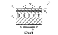
図1aは集積回路150の断面図を模式的に示しており、集積回路150は、適切なポリマー材質等の有機材質から実質的に構成されるパッケージ基板180に接続される半導体ダイ又はチップ100を備えており、ここではチップ100とパッケージ基板180の間の接続は、ピラー構造170によって達成され得る。半導体チップ100は、回路レイアウトの全体的な構造及び集積回路150の性能に応じて、基板101、例えばシリコン基板又はSOI基板を典型的には備えているであろう。また、シリコンベースの半導体層102が典型的には基板101の「上方」に設けられていてよく、この場合、半導体層102は、集積回路150の所望の機能的挙動に対して必要とされるトランジスタ、キャパシタ、抵抗等のような極めて多数の回路要素を備えているであろう。既に論じられたように、回路要素の臨界的寸法の継続的な縮小化は、大量生産技術により製造される現在利用可能な高度な半導体デバイスにおいては、50nmのオーダの、そしてそれより著しく小さなトランジスタの臨界的寸法をもたらし得る。半導体チップ100はメタライゼーションシステム110を備えており、進歩的なデバイスにおけるメタライゼーションシステム110は、複数のメタライゼーション層、即ち金属線及びビアが適切な誘電体材質内に組み込まれるデバイスレベルの複数のメタライゼーション層を含む。上で論じられたように、種々のメタライゼーション層内で用いられる対応する誘電体材質の少なくとも一部分は、隣接する金属線の寄生容量を減少させるために、機械的安定性の低い材質から通常は構成される。
FIG. 1a schematically illustrates a cross-sectional view of an integrated
前述したように、ピラー構造170はメタライゼーションシステム110の一部として提供することができ、この場合、対応する銅ピラーは、システム110の最後のメタライゼーション層内に形成される。一方、パッケージ基板180は適切に位置決めされ且つ寸法付けられたコンタクトパッド(図示せず)を備えており、熱及び/又は機械的圧力の印加によってそれぞれの機械的及び電気的な接続を確立するために、これらのコンタクトパッドは対応するピラー又はその上に形成された任意の半田材質に接触させられ得る。また、パッケージ基板180はピラー構造170の上部ピラー部分を対応する端子に接続するために適切な伝導線を通常は備えており、これによりプリント配線板等の他の周辺コンポーネントとの電気的なインタフェースが確立される。便宜上、そのような任意の伝導線は図示されていない。
As previously described, the
集積回路150の動作の間、例えば半導体層102内及びその上方に形成された回路要素によって半導体チップ100内に熱が生じる。この廃熱は、基板101の全体的な熱伝導性に応じて、例えばメタライゼーションシステム110及びピラー構造170によって高度に効率的な様態で且つ/又は基板101を介して消散される。例えば、SOI基板の放熱能力は、半導体層102を残りの基板材質から隔てている埋め込み絶縁酸化層の熱伝導性が低いことに起因して、純粋なシリコン基板と比較して著しく低い。従って、主たる放熱経路は、ピラー構造170及びパッケージ基板180によってもたらされる。その結果、適度に高い平均温度が半導体チップ100内で、またパッケージ基板180内でも生じ、この場合、既に論じられたように、これら2つの要素の間での熱膨張係数の不整合が顕著な機械的応力を生じさせ得る。例として矢印103及び183で示されるように、パッケージ基板180は半導体チップ100と比較して大きな熱膨張を有するであろうし、従って対応する不整合が、特に半導体チップ100とパッケージ基板180の間の「インタフェース、界面(interface)」で著しい程度の熱応力をもたらし、即ち、特にピラー構造170及びメタライゼーションシステム110は、集積回路150の動作の間、熱不整合による顕著なせん断力にさらされることになろう。洗練された誘電体材質の機械的安定性の低下及び密着性の低下に起因して、集積回路150の全体的な信頼性に影響する対応する欠陥が生じ得る。特にピラー構造170の個々のピラーの剛性が局部的に高いせん断力をもたらすことがあり、そのせん断力はメタライゼーションシステム内に転移するが、局部的に極めて限定された区域においては剥離欠陥等が生じ得る。
During operation of the
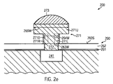
図1bはパッケージ基板180と半導体チップ100の間での顕著な熱的不整合の発生の間の状況を説明するために集積回路150の一部分を模式的に示している。図示されるように、最後のメタライゼーション層140が誘電体材質142を備えているであろうメタライゼーションシステム110の一部分が示されているであろうし、誘電体材質142内には、洗練された応用において銅材質からなるであろうコンタクトパッド141が埋め込まれている。また、最終不動態化層とも称されることがある不動態化層160が最後のメタライゼーション層140上に設けられており、不動態化層160はコンタクトパッド141の一部分を露出させている。更に、銅ピラーのような金属ピラー171が、最終不動態化層160からパッケージ基板180、即ちその内部に形成される対応するコンタクトパッド181まで延びているであろう。更に、典型的には半田材質173が金属ピラー171上に形成されているであろうし、半田材質173はコンタクトパッド181に接続しているであろう。更に、破線で示されるように、最終不動態化層160内に形成される開口は、通常は金属ピラー171の幅171Wよりも小さいであろうし、それにより金属ピラー171をコンタクトパッド141に接続するコンタクト領域172を形成し得る。従って、動作の間、せん断力183,103は、特に金属ピラー171の底部が最終不動態化層160と接触する対応する部分165で生じるある程度のトルクをもたらし得る。その結果、この区域においては、最大の機械的応力がメタライゼーションシステム110に局所的に選択的な様態で作用し得るので、主として区域165に由来するであろう対応する欠陥を余儀なくさせるであろう。
FIG. 1 b schematically illustrates a portion of the
従って、銅ピラーに基くチップとパッケージ基板の間の進歩的なコンタクト形態が、減少させられた必要な設置面積での放熱能力及び電気的伝導性に関する顕著な利益をもたらすことができ、それによりコンタクト要素及び/又は放熱のためのダミー要素の密度を高めることを可能にするものの、メタライゼーションシステム110内に生成される機械的応力の増大は、洗練された半導体デバイスの信頼性の要求とは両立し得ないかもしれない。この理由により、銅ピラーの高さはしばしば減少させられるが、このことはパッケージ基板とチップの間隔の減少を伴うので、任意のアンダーフィル(underfill)材質の信頼性のない充填の原因となることがある。このように、アンダーフィル材質内の対応するボイド(voids)は、例えば熱伝導性等における不均一性に起因する極めて低い信頼性の一因ともなり得る。他の従来の試みにおいては、メタライゼーションシステムの機械的な安定性を高めるために、それほど敏感でない低k誘電体材質又は超低k材質に基いてメタライゼーションシステムが形成されるかもしれないが、この場合、信号伝搬遅延の増大をもたらす寄生容量の増大に起因して、電気的な性能の著しい低下が伴う。
Thus, the progressive contact configuration between the chip and package substrate based on copper pillars can provide significant benefits in terms of heat dissipation capability and electrical conductivity in the reduced required footprint and thereby contact. Although it is possible to increase the density of elements and / or dummy elements for heat dissipation, the increased mechanical stress generated in the
上述した事情に鑑み、本開示は、ピラー構造を設けることができる一方で、上で特定した1つ以上の問題の影響を回避し又は少なくとも低減することができる方法及び半導体デバイスに関連している。 In view of the circumstances described above, the present disclosure relates to methods and semiconductor devices that can provide pillar structures while avoiding or at least reducing the effects of one or more of the problems identified above. .
概して本開示は、ピラー構造を介してメタライゼーションシステムへ転移する機械的応力の否定的な影響が、金属ピラーが最終不動態化層に接触する位置での最大力を減少させることによって低減され得る一方で、にもかからわず金属ピラーの上部で必要とされるコンタクト区域を維持することができる半導体デバイス及び製造技術に関連している。この目的で、ここに開示される幾つかの例示的な側面においては、金属ピラーの上部でのその横方向寸法は、パッケージ基板への接続を考慮した要求に適合するように選択されてよい一方で、金属ピラーの下部でのその横方向寸法、即ち最終不動態化層の表面に対応する高さでの金属ピラーの横方向寸法は、大幅に減少させられてよく、それにより、メタライゼーションシステム内へ転移される「点状(point-like)」応力を低減することもできる。このように、金属ピラーをくぎ状構造で設けることができ、くぎ状構造は金属堆積のプロセスを適切に修正することによって完成され得るが、全体的なプロセス複雑性に大きく影響することはない。 In general, the present disclosure can reduce the negative impact of mechanical stress transferred to the metallization system via the pillar structure by reducing the maximum force at the location where the metal pillar contacts the final passivation layer. On the other hand, it relates to semiconductor devices and manufacturing techniques that can nevertheless maintain the required contact area on top of the metal pillars. For this purpose, in some exemplary aspects disclosed herein, the lateral dimensions at the top of the metal pillar may be selected to meet the requirements considering connection to the package substrate. Thus, its lateral dimension at the bottom of the metal pillar, i.e. the lateral dimension of the metal pillar at a height corresponding to the surface of the final passivating layer, can be greatly reduced, so that the metallization system It is also possible to reduce the “point-like” stress transferred into the interior. In this way, the metal pillars can be provided in a nail-like structure, which can be completed by appropriately modifying the metal deposition process, but does not significantly affect the overall process complexity.
ここに開示される1つの例示的な半導体デバイスは、基板の上方に形成され且つ最終不動態化層を備えたメタライゼーションシステムを備えている。また、半導体デバイスは、最終不動態化層から延びる金属ピラーを備えており、ここでは金属ピラーは、メタライゼーションシステム内に形成されるコンタクトパッドに接触している。更に、金属ピラーは、最終不動態化層での第1の横方向寸法を有し且つその上面で第2の横方向寸法を有し、ここでは、第1の横方向寸法は第2の横方向寸法より小さい。 One exemplary semiconductor device disclosed herein comprises a metallization system formed over a substrate and with a final passivation layer. The semiconductor device also includes a metal pillar extending from the final passivation layer, where the metal pillar is in contact with a contact pad formed in the metallization system. In addition, the metal pillar has a first lateral dimension at the final passivation layer and a second lateral dimension at its top surface, where the first lateral dimension is the second lateral dimension. Smaller than directional dimension.
ここに開示される1つの例示的な方法は、第1の堆積マスクを半導体デバイスのメタライゼーションシステムの最終不動態化層の上方に形成することを備えており、ここでは、第1の堆積マスクは第1の幅を伴う第1の開口を有している。加えて、方法は、第1の堆積マスクの上方に第2の堆積マスクを形成することを備えており、ここでは、第2の堆積マスクは、第1の開口に対して位置合わせされる第2の開口を有しており、第2の開口は第1の幅よりも大きい第2の幅を伴う。最後に、方法は、第1及び第2の堆積マスクを用いて金属ピラーを形成することとを備えている。 One exemplary method disclosed herein comprises forming a first deposition mask over a final passivation layer of a semiconductor device metallization system, wherein the first deposition mask Has a first opening with a first width. In addition, the method comprises forming a second deposition mask over the first deposition mask, wherein the second deposition mask is aligned with the first opening. The second opening has a second width that is greater than the first width. Finally, the method comprises forming metal pillars using the first and second deposition masks.
ここに開示される更なる例示的な方法は、半導体デバイスを形成する方法に関連している。方法は、複数のメタライゼーション層の上方に最終不動態化層を形成することと、コンタクトパッドの一部分を露出させるように最終不動態化層内に開口を形成することとを備えている。加えて、方法は、最終不動態化層から延びるように金属ピラーを形成することを備えており、ここでは、金属ピラーは最終不動態化層の上面で第1の横方向寸法を有しており、金属ピラーはその上面で第2の横方向寸法を更に有しており、第1の横方向寸法は第2の横方向寸法に対して少なくとも30パーセントだけ第2の横方向寸法よりも小さい。 A further exemplary method disclosed herein relates to a method of forming a semiconductor device. The method comprises forming a final passivation layer over the plurality of metallization layers and forming an opening in the final passivation layer to expose a portion of the contact pad. In addition, the method comprises forming a metal pillar extending from the final passivation layer, wherein the metal pillar has a first lateral dimension on the top surface of the final passivation layer. The metal pillar further has a second lateral dimension on its upper surface, the first lateral dimension being at least 30 percent less than the second lateral dimension relative to the second lateral dimension. .
本開示の更なる実施形態は、添付の特許請求の範囲において画定されており、また添付の図面を参照したときに下記の詳細な説明と共に更に明らかになろう。 Further embodiments of the present disclosure are defined in the appended claims, and will become more apparent with reference to the following detailed description when taken in conjunction with the accompanying drawings.
以下の詳細な説明と共に図面に示される実施形態を参照して本開示が説明されるが、以下の詳細な説明及び図面は本開示を特定の例示的に開示されている実施形態に限定することを意図するものではなく、むしろ説明されている例示的な実施形態は単に本開示の種々の側面を例証しているにすぎず、本開示の範囲は添付の特許請求の範囲によって画定されていることが理解されるべきである。 The present disclosure will be described with reference to the embodiments illustrated in the drawings in conjunction with the following detailed description, which, however, limit the disclosure to certain exemplary disclosed embodiments. Rather, the exemplary embodiments described are merely illustrative of various aspects of the disclosure, and the scope of the disclosure is defined by the appended claims. It should be understood.
概して本開示は、メタライゼーションシステムに対する局部的な応力負荷を過度に増大することなしに、金属ピラーを含む洗練されたメタライゼーションシステムを効果的に用いることができる半導体デバイス及び技術を提供し、それにより、前述したように従来の誘電体と比較して低い機械的な安定性を有しているであろう高度に洗練された誘電体材質を用いる可能性がもたらされる。局部的な応力負荷又は力は、パッケージ基板に接続するためのコンタクト表面区域を提供することに関する所与の要求に対して、最終不動態化層に作用するトルク力を減少させることによって、効果的に減少させることができ、このことは、最終不動態化層と接触する区域での金属ピラーの横方向の寸法、即ち幅又は直径を適切に減少させる一方で、金属ピラーの少なくとも上面では所望のより大きな幅を設けることによって達成され得る。その結果、金属ピラーと最終不動態化層の誘電体材質の間の界面での既存のトルク力が減少させられ得るので、敏感な低k誘電体材質のような任意の下層の材質の局部的な負荷を低減することもでき、それにより、上述したように、半導体チップをパッケージ基板に接続するための製造プロセスの間の他、集積回路の動作の間にも全体的な安定性を高めることができる。ここに開示される幾つかの例示的な実施形態においては、金属ピラーの減少させられた横方向の寸法又は幅は、この横方向の幅が金属ピラーを最後のメタライゼーション層のコンタクトパッドに接続する接続区域の横方向の寸法にも実質的に対応するように選択されてよい一方で、他の場合には、接続区域は所望の直径に基いて形成されてよく、それよりも大きな幅を有するが従来のピラー構成に比べれば著しく減少させられた幅を有する金属ピラーの下部が続いて形成されてよく、それに続いて接続性等を考慮した要求に適合するために必要なより大きな横方向寸法を有する金属ピラーの上部が形成されてよい。 In general, this disclosure provides semiconductor devices and techniques that can effectively use sophisticated metallization systems, including metal pillars, without excessively increasing local stress loading on the metallization system, This provides the possibility of using highly sophisticated dielectric materials that will have a low mechanical stability compared to conventional dielectrics as described above. Local stress loads or forces are effective by reducing the torque force acting on the final passivation layer for a given requirement for providing a contact surface area for connection to the package substrate. Which can suitably reduce the lateral dimension, i.e., width or diameter, of the metal pillar in the area in contact with the final passivation layer, while at least on the top surface of the metal pillar as desired. This can be achieved by providing a larger width. As a result, the existing torque force at the interface between the metal pillar and the dielectric material of the final passivation layer can be reduced, so that any underlying material such as a sensitive low-k dielectric material can be localized. The overall stability during the operation of the integrated circuit as well as during the manufacturing process for connecting the semiconductor chip to the package substrate, as described above. Can do. In some exemplary embodiments disclosed herein, the reduced lateral dimension or width of the metal pillar is such that the lateral width connects the metal pillar to the contact pad of the last metallization layer. While the connection area may be selected to substantially correspond to the lateral dimensions of the connecting area, in other cases, the connecting area may be formed based on the desired diameter and have a larger width. A lower portion of a metal pillar having a width that is significantly reduced compared to conventional pillar configurations may be subsequently formed, followed by a larger lateral direction necessary to meet requirements such as connectivity etc. A top portion of a metal pillar having dimensions may be formed.
以下、図2a〜2eを参照して更に例示的な実施形態をより詳細に説明し、適切であれば図1a及び1bも参照する。 In the following, further exemplary embodiments will be described in more detail with reference to FIGS. 2a to 2e, with reference also to FIGS. 1a and 1b if appropriate.
図2aは進んだ製造段階における半導体デバイス200の断面図を模式的に示している。図示されるように、半導体デバイス200は、デバイス200の全体的な構成を考慮した要求に応じて、シリコン基板、SOI基板等のような基板201を備えていてよい。また、デバイスレベル又は半導体層202が基板201の上方に形成されていてよく、デバイスレベル又は半導体層202は、トランジスタ、キャパシタ、抵抗等の多数の回路要素を備えていてよく、これらはデバイス200に対応する適切な設計規則に基いて形成され得る。例えば、デバイスレベル202内の回路要素の臨界的寸法は概ね50nm以下であってよく、それにより洗練されたメタライゼーションシステムを必要としていてもよい。ここに開示される技術は複雑な半導体デバイスに関連して極めて有利であるが、ピラー構造を形成するための対応するレジームは、回路要素が50nm以上の臨界的寸法を有することのあるそれほど臨界的でない半導体デバイスにも有利に適用され得ることが理解されるべきである。更に、半導体デバイス200は、典型的には複数のメタライゼーション層220,…,240を含むメタライゼーションシステム210を備えていてよく、メタライゼーション層220,…,240の少なくとも幾つかは、幾つかの例示的な実施形態では、前述したような敏感な誘電体材質を備えている。また、最後のメタライゼーション層240は、コンタクトパッド241の形態にある金属領域がその内部に形成されたものであってよく、コンタクトパッド241は、銅、アルミニウム、銅/アルミニウム、等のような任意の適切な材質から構成されていてよい。洗練されたメタライゼーションシステムにおいては、金属線及びビアは、前述したように熱的及び電気的な伝導性を考慮する場合における優れた特性により、銅材質に基いて設けられていてよいことが理解されるべきである。しかし、場合によっては他の金属と組み合わされるアルミニウム、銀、等のような他の材質を含むメタライゼーションシステムがここで検討されてもよいことが注目されるべきである。また、周囲の材質242との金属の接触が不適切であろうと考えられる場合には、銅のような対応する金属を確実に閉じ込めるために、コンタクトパッド241は必要に応じて任意の適切なバリア材質を備えていてよい。
FIG. 2a schematically shows a cross-sectional view of the
更に、最終不動態化層260が最後のメタライゼーション層240の上方に形成されていてよく、そして最終不動態化層260は、不動態化、機械的な完全性、等に関する全体的な特性を考慮した必要性に応じて2つ以上のサブ層261,262を備えていてよい。例えば、第1のサブ層261は二酸化シリコン、窒化シリコン等から構成されてよい一方、第2のサブ層262はポリアミド等のような不動態化材質を代表してよい。図示される製造段階においては、開口263がコンタクトパッド241まで延びるように最終不動態化層260内に形成されていてよく、ここでは、開口263の対応する横方向寸法及び最終不動態化層260の厚みは、最終不動態化層260の及び開口263の対応する特性が、最終不動態化層260の上方にピラーを形成するための標準的な戦略に適合し得るように、十分に確立されたプロセス戦略に従って選択されてよい。他の場合には、開口の幅は、必要に応じて従来の設計戦略と比較して小さく選択されてよい。また、第1の堆積マスク264が設けられてよく、マスク264に基いて形成されることになる金属ピラーの第1の部分の位置及び横方向のサイズを規定することができる。この目的で、堆積マスク264は、適切に選択された横方向寸法又は幅264Wを有する開口264Aを備えており、幅264Wは、別の面では同一のデバイス要求に対する従来の金属ピラーと比較して大幅に小さくてよい。実例として、対応する従来の横方向寸法が破線264Cで示されている。例えば、従来の幅264Cは、前述したように、パッケージ基板に接続するために必要とされる所望の断面積に実質的に対応していてよい。実例としては、概ね100〜30μmの直径を伴うコンタクト表面積が必要とされるであろう場合、即ち従来の幅264Cが概ね100〜30μmに選択されたであろう場合、開口264Aの幅264Wは、更に形成されることになる金属ピラーのコンタクト表面で必要とされる横方向寸法に対して概ね70パーセント以下、例えば50パーセント以下に選択されてよい。更に、堆積マスク264の厚み264Tは、減少させられた横方向寸法を有する金属ピラーの部分の望ましい高さに対応するように選択されてよい。例えば、厚み264Tは、更に形成されることになる金属ピラーの最終的な高さの概ね半分に対応していてよい一方で、他の場合には、更に減少させられた厚みが必要に応じて選択されてよい。
In addition, a
図2aに示される半導体デバイス200は以下のプロセス戦略に基いて形成することができる。先ず、デバイスレベル202内の回路要素の他、メタライゼーション層220、230及び240を含むメタライゼーションシステム210は、任意の適切なプロセス戦略に基いて形成することができ、ここでは必要に応じて所望の技術標準及びプロセス技術との高度な互換性が維持されてよい。その後、例えばサブ層261及び262のような対応する誘電体材質を堆積させると共に次いでこれらを十分に確立されたリソグラフィ技術によりパターニングすることによって、最終不動態化層260を形成することができる。例えば、ポリイミド材質262は、感光性材質の形態で設けられてよく、そして対応する現像プロセスによってパターニングされてよく、それに続いて層261がエッチングされてよい。他の場合には、対応するレジストマスクが、コンタクトパッド241の部分を露出させるために最終不動態化層260を通ってエッチングするように設けられてよい。最終不動態化層260の材質との直接の接触が不適切であろうと考えられる場合には、銅のような対応する反応性金属を閉じ込めるために、必要に応じて任意の適切なバリア材質265が堆積させられてよい。また、開口263内並びに最終不動態化層260の上面260S及び側壁260Wの露出させられた部分上に形成されるべき金属の密着性の向上を考慮すると、層265は有利であろう。この目的のために、クロム、銅、タンタル、タンタル窒化物、等のような任意の適切な材質、又は種々の材質の組み合わせを用いることができる。その後、堆積マスク264が例えばレジスト材質の形態で設けられてよく、ここでは、その厚みは所望の目標厚み264Tを得るように選択されてよい。幾つかの例示的な実施形態では、マスク材質を設けた後に、所望の目標厚み264Tを得るように平坦化プロセスが実行されてよい。その後、減少させられた幅264Wを得るために、適切なリソグラフィマスクを用いることによって、開口264Aがパターニングされてよい。
The
図2bは更に進んだ製造段階における半導体デバイス200を模式的に示している。図示されるように、堆積マスク264の上方には第2の堆積マスク266が形成されてよく、第2の堆積マスク266内には開口266Aが形成されていてよく、開口266Aは、開口264A及び263に対して位置合わせされると共に、開口264A,266Aに基いて更に形成されることになる金属ピラーの一部分の横方向の位置並びにサイズ及び形状を規定し得る。その結果、開口266Aの幅266W及び全体的な形状は、図1a及び1bにおける集積回路150に関しても既に論じられたように、パッケージ基板に接続するための金属ピラーに対する要求に適合するように選択されてよい。従って、幾つかの例示的な実施形態では、高度に洗練された応用が考えられる場合に、幅266Wは100〜30μmの範囲内にあってよい。寸法264Wに対して顕著に増大された寸法266Wに起因して、開口266A,264Aに基いて形成されることになる金属ピラーは、最終不動態化層260に作用する局部的トルク力を低減するために、「くぎ状(nail-like)」構造を有することができる。また、場合によっては必要に応じて半田材質等のような付加的な材質と組み合わせられて更に形成されることになる金属ピラーの上部の厚みを収容するように、堆積マスク266が任意の適切な厚みで設けられてよい。堆積マスクはレジスト材質の形態で設けられてよく、レジスト材質は、十分に確立されたリソグラフィ技術を用いることによって、即ちプロセス戦略に応じてポジティブレジスト又はネガティブレジストを設けると共にレジスト材質の露光された部分又は露光されなかった部分を除去することによってパターニングされ得る。その後、必要であれば、場合によっては対応するバリア材質(図示せず)、例えば図2aを参照して説明したようなバリア材質265との組み合わせにおけるコンタクトパッド241の露出させられた表面を準備するように、ウエット化学的洗浄プロセスが実行されてよい。
FIG. 2b schematically shows the
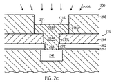
図2cは堆積環境205に曝されるときの半導体デバイス200を模式的に示しており、堆積環境205の間、金属ピラー271を形成するように適切な金属材質が開口266A,264A内に充填されてよい。理解されるべきことは、図2a〜2cに示される実施形態においては、堆積プロセス205の間に接続要素272が開口263内に形成されてもよく、その結果、接続要素272及び金属ピラー271は同一の材質に基いて形成することができ、ピラー271は開口264Aによって規定される寸法を伴う下部271Lと開口266Aによって規定される寸法を有する上部271Uとを備えていることである。他の場合には、接続部分272は、適切であると考えられる場合には、金属ピラー271とは別に形成されてよい。例えば、最終不動態化層260及び開口263に基き電気化学的堆積技術によって特定の材質が堆積させられてよく、その後に、所望の構造を伴い且つ特定の金属材質に基く金属ピラー271を設けるために、第1及び第2の堆積マスク264及び266が形成されてよい。
FIG. 2 c schematically illustrates the
堆積プロセス205は、無電解メッキ、電気メッキ等のような任意の適切な電気化学的堆積技術を備えていてよく、幾つかの例示的な実施形態では、金属ピラー271を完成させた後にパターニングされる必要があるであろう対応する電流分配層を伴わない無電解メッキ技術が用いられてよい。この目的で、多くの十分に確立された堆積レシピが利用可能である。幾つかの例示的な実施形態では、例えば後続の製造段階等においてパッケージ基板のコンタクトパッドに直接的に接続するための対応するプロセスの間における性能を高めることを考慮して、必要であれば追加的なキャップ材質が上面271S上に形成されてよい。
The
図2dは更なる例示的な実施形態に従う半導体デバイス200を模式的に示しており、その実施形態においては、例えば鉛フリー半田材質のような半田材質の形態にある更なる材質273が電気化学的堆積プロセスのような堆積プロセス206の間に堆積させられてよく、堆積プロセス206のためには十分に確立された堆積レシピが利用可能である。この目的で、金属ピラー271即ちその上部271Uと材質273の所望の厚みとを収容するように、堆積マスク266の厚みが適切に選択されてよい。その後、堆積マスク266及び264がプラズマストリッピング等のような任意の適切なエッチング技術によって除去されてよく、設けられている場合における電流分配層の部分、バリア材質、等を除去するように任意の更なるエッチングプロセスがそれに続いてよい。そのような材質が最終不動態化層260から除去される必要があるであろう場合には、適切な等方性エッチングレシピが用いられてよく、その結果、上部271Uの陰影効果が任意のそのような材質の効果的な除去に否定的に影響することはないであろうことが理解されるべきである。
FIG. 2d schematically illustrates a
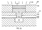
図2eは幾つかの例示的な実施形態に従い更に進んだ製造段階における半導体デバイス200を模式的に示している。図示されるように、デバイス200は金属ピラー271を備えていてよく、金属ピラー271は、上で指定されるように選択され得るそれぞれ横方向寸法266W及び264Wを伴う上部271U及び下部271Lを含んでいる。また、図示される実施形態においては、半田材質の形態にある追加的な材質273が金属ピラー271の上方に形成されていてよく、追加的な材質273は、図示される実施形態においては、先行して堆積させられた半田材質をリフローすることで得られる強化された形状を有していてよい。他の実施形態においては、金属ピラー271は図2cに示されるように追加的な半田材質を伴うことなしに設けられてよく、あるいは半田材質273が設けられている場合には図2dに示されるようにそのリフローが省略されてよい。図示されるように、幾つかの実施形態では、部分271Rによって示されるように、金属ピラー271の少なくとも一部分が最終不動態化層260の上方に「残って(rest)」いることができるように、減少させられた横方向寸法264Wが選択されてよい。この場合、減少させられた幅264W全体により、前述したように、最終不動態化層260の表面に作用する対応する機械的な力が低減され得る。その結果、最終不動態化層260の下方に位置する任意の材質に作用する対応する局部的機械的応力もまた低減され得るので、層間剥離、亀裂等のような欠陥を生成する蓋然性を低くすることができる。他の例示的な実施形態においては、寸法264Wは接続要素272の横方向寸法263Wに実質的に対応するように選択されてよく、それにより、最終不動態化層260に作用するように結果として局部的に生じる力を低減することもできる。更に他の実施形態においては、横方向寸法264Wは271Dで示されるように寸法263Wよりも小さく設定されてよく、それにより、不動態化層260の表面260Sとの金属ピラー271の相互作用を実質的に完全に回避することができる。横方向幅264Wの対応する変化は、堆積マスク264(図2b参照)の開口264Aの幅を適切に選択することによって達成され得ることが理解されるべきである。
FIG. 2e schematically illustrates the
結果として、本開示は、金属ピラーの下部の横方向寸法を減少させることによって不動態化材質の表面と金属ピラーとの界面での局部的な力が低減され得る一方で、その上部でパッケージ基板に接続するための所望の表面区域は維持することができる半導体デバイス及び製造技術を提供する。その結果、従来の半田材質と比較して高い剛性を有する任意の所望の材質、例えば銅、銅合金、ニッケル等を用いることができる一方で、金属ピラー構造の全体的な接続性に妥協することなしにメタライゼーションシステム内で洗練された誘電体材質を用いる可能性をもたらすこともできる。 As a result, the present disclosure can reduce the local force at the interface between the surface of the passivating material and the metal pillar by reducing the lateral dimension of the lower part of the metal pillar, while the package substrate above it. Semiconductor devices and manufacturing techniques that can maintain a desired surface area for connection to a semiconductor device are provided. As a result, any desired material with higher rigidity compared to conventional solder materials, such as copper, copper alloys, nickel, etc., can be used while compromising the overall connectivity of the metal pillar structure. Without the possibility of using sophisticated dielectric materials within the metallization system.
本開示の更なる修正及び変更は、この明細書を考慮することによって当業者には明白になろう。従って、明細書は、例示的なものとしてのみ解釈されるべきであり、またここに開示される原理を実施する一般的な手法を当業者に教示することを目的としている。ここに示されまた説明される形態は目下のところ望ましい実施形態として解釈されるべきことが理解されるべきである。 Further modifications and variations of the present disclosure will become apparent to those skilled in the art from consideration of this specification. Accordingly, the specification is to be construed as illustrative only and is for the purpose of teaching those skilled in the art the general manner of carrying out the principles disclosed herein. It should be understood that the form shown and described herein is to be construed as the presently preferred embodiment.
Claims (25)
前記最終不動態化層から延び前記メタライゼーションシステム内に形成されるコンタクトパッドに接触する金属ピラーとを備えた半導体デバイスであって、
前記金属ピラーは、前記最終不動態化層での第1の横方向寸法を有し且つその上面で第2の横方向寸法を有し、前記第1の横方向寸法は前記第2の横方向寸法より小さい半導体デバイス。 A metallization system formed above the substrate and comprising a final passivation layer;
A semiconductor device comprising a metal pillar extending from the final passivation layer and contacting a contact pad formed in the metallization system,
The metal pillar has a first lateral dimension at the final passivation layer and a second lateral dimension at the top surface, the first lateral dimension being the second lateral dimension. A semiconductor device smaller than the size.
前記第1の開口に対して位置合わせされる第2の開口を有し前記第2の開口は前記第1の幅よりも大きい第2の幅を有している第2の堆積マスクを前記第1の堆積マスクの上方に形成することと、
前記第1及び第2の堆積マスクを用いて金属ピラーを形成することとを備えた方法。 Forming a first deposition mask having a first opening with a first width over a final passivation layer of a semiconductor device metallization system;
A second deposition mask having a second opening aligned with the first opening, wherein the second opening has a second width greater than the first width; Forming above one deposition mask;
Forming metal pillars using the first and second deposition masks.
複数のメタライゼーション層の上方に最終不動態化層を形成することと、
コンタクトパッドの一部分を露出させるように前記最終不動態化層内に開口を形成することと、
前記最終不動態化層から延びるように金属ピラーを形成することとを備え、
前記金属ピラーは前記最終不動態化層の上面で第1の横方向寸法を有しており、前記金属ピラーはその上面で第2の横方向寸法を更に有しており、前記第1の横方向寸法は前記第2の横方向寸法に対して少なくとも30パーセントだけ前記第2の横方向寸法よりも小さい方法。 A method of forming a semiconductor device comprising:
Forming a final passivation layer above the plurality of metallization layers;
Forming an opening in the final passivation layer to expose a portion of the contact pad;
Forming metal pillars extending from the final passivation layer,
The metal pillar has a first lateral dimension on the top surface of the final passivation layer, the metal pillar further has a second lateral dimension on the top surface, and the first lateral dimension. The direction dimension is less than the second lateral dimension by at least 30 percent relative to the second lateral dimension.
Applications Claiming Priority (3)
| Application Number | Priority Date | Filing Date | Title |
|---|---|---|---|
| DE102009010885.8 | 2009-02-27 | ||
| DE102009010885.8A DE102009010885B4 (en) | 2009-02-27 | 2009-02-27 | Metallization system of a semiconductor device with metal columns with a smaller diameter at the bottom and manufacturing method thereof |
| PCT/EP2010/001092 WO2010097191A1 (en) | 2009-02-27 | 2010-02-22 | A metallization system of a semiconductor device including metal pillars having a reduced diameter at the bottom |
Publications (2)
| Publication Number | Publication Date |
|---|---|
| JP2012519374A true JP2012519374A (en) | 2012-08-23 |
| JP2012519374A5 JP2012519374A5 (en) | 2013-04-11 |
Family
ID=42102254
Family Applications (1)
| Application Number | Title | Priority Date | Filing Date |
|---|---|---|---|
| JP2011551432A Pending JP2012519374A (en) | 2009-02-27 | 2010-02-22 | Semiconductor device metallization system including metal pillars with decreasing diameter at the bottom |
Country Status (6)
| Country | Link |
|---|---|
| US (1) | US9245860B2 (en) |
| JP (1) | JP2012519374A (en) |
| KR (1) | KR20110128897A (en) |
| CN (1) | CN102428551A (en) |
| DE (1) | DE102009010885B4 (en) |
| WO (1) | WO2010097191A1 (en) |
Families Citing this family (8)
| Publication number | Priority date | Publication date | Assignee | Title |
|---|---|---|---|---|
| US8314472B2 (en) | 2010-07-29 | 2012-11-20 | Avago Technologies Wireless Ip (Singapore) Pte. Ltd. | Semiconductor structure comprising pillar |
| US8344504B2 (en) | 2010-07-29 | 2013-01-01 | Avago Technologies Wireless Ip (Singapore) Pte. Ltd. | Semiconductor structure comprising pillar and moisture barrier |
| US20120273937A1 (en) * | 2011-04-30 | 2012-11-01 | Stats Chippac, Ltd. | Semiconductor Device and Method of Forming Bump Interconnect Structure with Conductive Layer Over Buffer Layer |
| US8536707B2 (en) | 2011-11-29 | 2013-09-17 | Avago Technologies General Ip (Singapore) Pte. Ltd. | Semiconductor structure comprising moisture barrier and conductive redistribution layer |
| US9768142B2 (en) | 2013-07-17 | 2017-09-19 | Taiwan Semiconductor Manufacturing Company, Ltd. | Mechanisms for forming bonding structures |
| US10049893B2 (en) | 2016-05-11 | 2018-08-14 | Advanced Semiconductor Engineering, Inc. | Semiconductor device with a conductive post |
| US10636758B2 (en) | 2017-10-05 | 2020-04-28 | Texas Instruments Incorporated | Expanded head pillar for bump bonds |
| KR20210121336A (en) | 2020-03-26 | 2021-10-08 | 삼성전자주식회사 | Semiconductor package |
Citations (6)
| Publication number | Priority date | Publication date | Assignee | Title |
|---|---|---|---|---|
| JPH0555228A (en) * | 1991-08-27 | 1993-03-05 | Nec Corp | Semiconductor device |
| JPH05206139A (en) * | 1991-11-19 | 1993-08-13 | Nec Corp | Substrate connection electrode and manufacture of the same |
| JP2000228420A (en) * | 1999-02-05 | 2000-08-15 | Sanyo Electric Co Ltd | Semiconductor device and manufacture thereof |
| JP2002076046A (en) * | 2000-09-04 | 2002-03-15 | Citizen Watch Co Ltd | Method for manufacturing semiconductor device |
| JP2006295109A (en) * | 2005-03-14 | 2006-10-26 | Citizen Watch Co Ltd | Semiconductor device and manufacturing method thereof |
| JP2010525553A (en) * | 2007-02-28 | 2010-07-22 | ネペス コーポレーション | Bump structure of semiconductor device |
Family Cites Families (13)
| Publication number | Priority date | Publication date | Assignee | Title |
|---|---|---|---|---|
| US5137597A (en) * | 1991-04-11 | 1992-08-11 | Microelectronics And Computer Technology Corporation | Fabrication of metal pillars in an electronic component using polishing |
| JP2773578B2 (en) * | 1992-10-02 | 1998-07-09 | 日本電気株式会社 | Method for manufacturing semiconductor device |
| US5656858A (en) * | 1994-10-19 | 1997-08-12 | Nippondenso Co., Ltd. | Semiconductor device with bump structure |
| US5912510A (en) * | 1996-05-29 | 1999-06-15 | Motorola, Inc. | Bonding structure for an electronic device |
| US5773897A (en) * | 1997-02-21 | 1998-06-30 | Raytheon Company | Flip chip monolithic microwave integrated circuit with mushroom-shaped, solder-capped, plated metal bumps |
| US5891756A (en) * | 1997-06-27 | 1999-04-06 | Delco Electronics Corporation | Process for converting a wire bond pad to a flip chip solder bump pad and pad formed thereby |
| JP3420703B2 (en) * | 1998-07-16 | 2003-06-30 | 株式会社東芝 | Method for manufacturing semiconductor device |
| US6103552A (en) * | 1998-08-10 | 2000-08-15 | Lin; Mou-Shiung | Wafer scale packaging scheme |
| US6818545B2 (en) * | 2001-03-05 | 2004-11-16 | Megic Corporation | Low fabrication cost, fine pitch and high reliability solder bump |
| TWI244129B (en) * | 2002-10-25 | 2005-11-21 | Via Tech Inc | Bonding column process |
| JP4119866B2 (en) * | 2004-05-12 | 2008-07-16 | 富士通株式会社 | Semiconductor device |
| TWI242253B (en) * | 2004-10-22 | 2005-10-21 | Advanced Semiconductor Eng | Bumping process and structure thereof |
| US8709934B2 (en) * | 2007-06-05 | 2014-04-29 | Stats Chippac Ltd. | Electronic system with vertical intermetallic compound |
-
2009
- 2009-02-27 DE DE102009010885.8A patent/DE102009010885B4/en active Active
-
2010
- 2010-02-22 JP JP2011551432A patent/JP2012519374A/en active Pending
- 2010-02-22 WO PCT/EP2010/001092 patent/WO2010097191A1/en active Application Filing
- 2010-02-22 KR KR1020117022596A patent/KR20110128897A/en not_active Application Discontinuation
- 2010-02-22 CN CN2010800183996A patent/CN102428551A/en active Pending
- 2010-02-23 US US12/710,458 patent/US9245860B2/en active Active
Patent Citations (6)
| Publication number | Priority date | Publication date | Assignee | Title |
|---|---|---|---|---|
| JPH0555228A (en) * | 1991-08-27 | 1993-03-05 | Nec Corp | Semiconductor device |
| JPH05206139A (en) * | 1991-11-19 | 1993-08-13 | Nec Corp | Substrate connection electrode and manufacture of the same |
| JP2000228420A (en) * | 1999-02-05 | 2000-08-15 | Sanyo Electric Co Ltd | Semiconductor device and manufacture thereof |
| JP2002076046A (en) * | 2000-09-04 | 2002-03-15 | Citizen Watch Co Ltd | Method for manufacturing semiconductor device |
| JP2006295109A (en) * | 2005-03-14 | 2006-10-26 | Citizen Watch Co Ltd | Semiconductor device and manufacturing method thereof |
| JP2010525553A (en) * | 2007-02-28 | 2010-07-22 | ネペス コーポレーション | Bump structure of semiconductor device |
Also Published As
| Publication number | Publication date |
|---|---|
| DE102009010885A1 (en) | 2010-09-02 |
| US9245860B2 (en) | 2016-01-26 |
| DE102009010885B4 (en) | 2014-12-31 |
| KR20110128897A (en) | 2011-11-30 |
| US20100219527A1 (en) | 2010-09-02 |
| WO2010097191A1 (en) | 2010-09-02 |
| CN102428551A (en) | 2012-04-25 |
Similar Documents
| Publication | Publication Date | Title |
|---|---|---|
| CN110034026B (en) | Package structure and method | |
| US9240349B2 (en) | Interconnect structures for substrate | |
| TWI557820B (en) | Device package and methods of forming the same | |
| US8039958B2 (en) | Semiconductor device including a reduced stress configuration for metal pillars | |
| US8450206B2 (en) | Method of forming a semiconductor device including a stress buffer material formed above a low-k metallization system | |
| TWI718722B (en) | Bonding structure and method of forming same | |
| US9245860B2 (en) | Metallization system of a semiconductor device including metal pillars having a reduced diameter at the bottom | |
| TW202123413A (en) | Device having bonding structure and package and method of forming bonding structure | |
| US8482123B2 (en) | Stress reduction in chip packaging by using a low-temperature chip-package connection regime | |
| US20100164098A1 (en) | Semiconductor device including a cost-efficient chip-package connection based on metal pillars | |
| KR20190024570A (en) | Conductive vias in semiconductor packages and methods of forming same | |
| US8941238B2 (en) | Semiconductor device | |
| TWI764681B (en) | Semiconductor package, package component, and method of manufacturing | |
| US8786088B2 (en) | Semiconductor device including ultra low-K (ULK) metallization stacks with reduced chip-package interaction | |
| US9136234B2 (en) | Semiconductor device with improved metal pillar configuration | |
| TW202137354A (en) | Semiconductor device and formation method thereof | |
| TWI483314B (en) | Protection of reactive metal surfaces of semiconductor devices during shipping by providing an additional protection layer | |
| WO2010049087A2 (en) | A semiconductor device including a reduced stress configuration for metal pillars | |
| TWI749920B (en) | Semicondutor package and method of forming same | |
| TWI773400B (en) | Semiconductor device and manufacturing method thereof | |
| TWI825572B (en) | Chip package structure and method for forming the same | |
| TWI822153B (en) | Package structure and method for forming the same | |
| TWI809607B (en) | Semiconductor device with stacked chips and method for fabricating the same | |
| TWI792433B (en) | Semiconductor device and method for manufacturing semiconductor device | |
| TWI801938B (en) | Semiconductor package and method of forming the same |
Legal Events
| Date | Code | Title | Description |
|---|---|---|---|
| A521 | Request for written amendment filed |
Free format text: JAPANESE INTERMEDIATE CODE: A523 Effective date: 20130221 |
|
| A621 | Written request for application examination |
Free format text: JAPANESE INTERMEDIATE CODE: A621 Effective date: 20130221 |
|
| A977 | Report on retrieval |
Free format text: JAPANESE INTERMEDIATE CODE: A971007 Effective date: 20131216 |
|
| A131 | Notification of reasons for refusal |
Free format text: JAPANESE INTERMEDIATE CODE: A131 Effective date: 20140205 |
|
| A521 | Request for written amendment filed |
Free format text: JAPANESE INTERMEDIATE CODE: A523 Effective date: 20140507 |
|
| A02 | Decision of refusal |
Free format text: JAPANESE INTERMEDIATE CODE: A02 Effective date: 20140625 |