JP2012507874A - Optoelectronic devices based on nonpolar or semipolar AlInN and AlInGaN alloys - Google Patents
Optoelectronic devices based on nonpolar or semipolar AlInN and AlInGaN alloys Download PDFInfo
- Publication number
- JP2012507874A JP2012507874A JP2011534857A JP2011534857A JP2012507874A JP 2012507874 A JP2012507874 A JP 2012507874A JP 2011534857 A JP2011534857 A JP 2011534857A JP 2011534857 A JP2011534857 A JP 2011534857A JP 2012507874 A JP2012507874 A JP 2012507874A
- Authority
- JP
- Japan
- Prior art keywords
- layer
- quantum well
- nonpolar
- semipolar
- light emitting
- Prior art date
- Legal status (The legal status is an assumption and is not a legal conclusion. Google has not performed a legal analysis and makes no representation as to the accuracy of the status listed.)
- Pending
Links
Images


Classifications
-
- H—ELECTRICITY
- H01—ELECTRIC ELEMENTS
- H01L—SEMICONDUCTOR DEVICES NOT COVERED BY CLASS H10
- H01L33/00—Semiconductor devices with at least one potential-jump barrier or surface barrier specially adapted for light emission; Processes or apparatus specially adapted for the manufacture or treatment thereof or of parts thereof; Details thereof
- H01L33/02—Semiconductor devices with at least one potential-jump barrier or surface barrier specially adapted for light emission; Processes or apparatus specially adapted for the manufacture or treatment thereof or of parts thereof; Details thereof characterised by the semiconductor bodies
- H01L33/26—Materials of the light emitting region
- H01L33/30—Materials of the light emitting region containing only elements of group III and group V of the periodic system
-
- B—PERFORMING OPERATIONS; TRANSPORTING
- B82—NANOTECHNOLOGY
- B82Y—SPECIFIC USES OR APPLICATIONS OF NANOSTRUCTURES; MEASUREMENT OR ANALYSIS OF NANOSTRUCTURES; MANUFACTURE OR TREATMENT OF NANOSTRUCTURES
- B82Y20/00—Nanooptics, e.g. quantum optics or photonic crystals
-
- H—ELECTRICITY
- H01—ELECTRIC ELEMENTS
- H01L—SEMICONDUCTOR DEVICES NOT COVERED BY CLASS H10
- H01L33/00—Semiconductor devices with at least one potential-jump barrier or surface barrier specially adapted for light emission; Processes or apparatus specially adapted for the manufacture or treatment thereof or of parts thereof; Details thereof
- H01L33/02—Semiconductor devices with at least one potential-jump barrier or surface barrier specially adapted for light emission; Processes or apparatus specially adapted for the manufacture or treatment thereof or of parts thereof; Details thereof characterised by the semiconductor bodies
- H01L33/16—Semiconductor devices with at least one potential-jump barrier or surface barrier specially adapted for light emission; Processes or apparatus specially adapted for the manufacture or treatment thereof or of parts thereof; Details thereof characterised by the semiconductor bodies with a particular crystal structure or orientation, e.g. polycrystalline, amorphous or porous
-
- H—ELECTRICITY
- H01—ELECTRIC ELEMENTS
- H01L—SEMICONDUCTOR DEVICES NOT COVERED BY CLASS H10
- H01L33/00—Semiconductor devices with at least one potential-jump barrier or surface barrier specially adapted for light emission; Processes or apparatus specially adapted for the manufacture or treatment thereof or of parts thereof; Details thereof
- H01L33/02—Semiconductor devices with at least one potential-jump barrier or surface barrier specially adapted for light emission; Processes or apparatus specially adapted for the manufacture or treatment thereof or of parts thereof; Details thereof characterised by the semiconductor bodies
- H01L33/26—Materials of the light emitting region
- H01L33/30—Materials of the light emitting region containing only elements of group III and group V of the periodic system
- H01L33/32—Materials of the light emitting region containing only elements of group III and group V of the periodic system containing nitrogen
-
- H—ELECTRICITY
- H01—ELECTRIC ELEMENTS
- H01S—DEVICES USING THE PROCESS OF LIGHT AMPLIFICATION BY STIMULATED EMISSION OF RADIATION [LASER] TO AMPLIFY OR GENERATE LIGHT; DEVICES USING STIMULATED EMISSION OF ELECTROMAGNETIC RADIATION IN WAVE RANGES OTHER THAN OPTICAL
- H01S5/00—Semiconductor lasers
- H01S5/30—Structure or shape of the active region; Materials used for the active region
- H01S5/34—Structure or shape of the active region; Materials used for the active region comprising quantum well or superlattice structures, e.g. single quantum well [SQW] lasers, multiple quantum well [MQW] lasers or graded index separate confinement heterostructure [GRINSCH] lasers
- H01S5/343—Structure or shape of the active region; Materials used for the active region comprising quantum well or superlattice structures, e.g. single quantum well [SQW] lasers, multiple quantum well [MQW] lasers or graded index separate confinement heterostructure [GRINSCH] lasers in AIIIBV compounds, e.g. AlGaAs-laser, InP-based laser
- H01S5/34333—Structure or shape of the active region; Materials used for the active region comprising quantum well or superlattice structures, e.g. single quantum well [SQW] lasers, multiple quantum well [MQW] lasers or graded index separate confinement heterostructure [GRINSCH] lasers in AIIIBV compounds, e.g. AlGaAs-laser, InP-based laser with a well layer based on Ga(In)N or Ga(In)P, e.g. blue laser
-
- H—ELECTRICITY
- H01—ELECTRIC ELEMENTS
- H01S—DEVICES USING THE PROCESS OF LIGHT AMPLIFICATION BY STIMULATED EMISSION OF RADIATION [LASER] TO AMPLIFY OR GENERATE LIGHT; DEVICES USING STIMULATED EMISSION OF ELECTROMAGNETIC RADIATION IN WAVE RANGES OTHER THAN OPTICAL
- H01S5/00—Semiconductor lasers
- H01S5/20—Structure or shape of the semiconductor body to guide the optical wave ; Confining structures perpendicular to the optical axis, e.g. index or gain guiding, stripe geometry, broad area lasers, gain tailoring, transverse or lateral reflectors, special cladding structures, MQW barrier reflection layers
- H01S5/2004—Confining in the direction perpendicular to the layer structure
- H01S5/2009—Confining in the direction perpendicular to the layer structure by using electron barrier layers
-
- H—ELECTRICITY
- H01—ELECTRIC ELEMENTS
- H01S—DEVICES USING THE PROCESS OF LIGHT AMPLIFICATION BY STIMULATED EMISSION OF RADIATION [LASER] TO AMPLIFY OR GENERATE LIGHT; DEVICES USING STIMULATED EMISSION OF ELECTROMAGNETIC RADIATION IN WAVE RANGES OTHER THAN OPTICAL
- H01S5/00—Semiconductor lasers
- H01S5/30—Structure or shape of the active region; Materials used for the active region
- H01S5/32—Structure or shape of the active region; Materials used for the active region comprising PN junctions, e.g. hetero- or double- heterostructures
- H01S5/3201—Structure or shape of the active region; Materials used for the active region comprising PN junctions, e.g. hetero- or double- heterostructures incorporating bulkstrain effects, e.g. strain compensation, strain related to polarisation
-
- H—ELECTRICITY
- H01—ELECTRIC ELEMENTS
- H01S—DEVICES USING THE PROCESS OF LIGHT AMPLIFICATION BY STIMULATED EMISSION OF RADIATION [LASER] TO AMPLIFY OR GENERATE LIGHT; DEVICES USING STIMULATED EMISSION OF ELECTROMAGNETIC RADIATION IN WAVE RANGES OTHER THAN OPTICAL
- H01S5/00—Semiconductor lasers
- H01S5/30—Structure or shape of the active region; Materials used for the active region
- H01S5/32—Structure or shape of the active region; Materials used for the active region comprising PN junctions, e.g. hetero- or double- heterostructures
- H01S5/3211—Structure or shape of the active region; Materials used for the active region comprising PN junctions, e.g. hetero- or double- heterostructures characterised by special cladding layers, e.g. details on band-discontinuities
Abstract
280nmから360nmの範囲の放射波長(λpeak)を伴う、高出力および高効率発光デバイスを製造する。新しいデバイス構造は、無極性または半極性バルクGaN基板上に成長させられる、無極性または半極性AlInNおよびAlInGaN合金を使用する。一実施形態において、光電子デバイスは、無極性または半極性GaN基板上に成長させられる、少なくとも、アルミニウム(Al)、インジウム(In)、および窒素(N)を含有する1つ以上の発光層を備える光電子デバイスであって、該発光層は、無極性または半極性層である。A high power and high efficiency light emitting device with a radiation wavelength (λ peak ) in the range of 280 nm to 360 nm is manufactured. New device structures use nonpolar or semipolar AlInN and AlInGaN alloys grown on nonpolar or semipolar bulk GaN substrates. In one embodiment, the optoelectronic device comprises one or more light-emitting layers containing at least aluminum (Al), indium (In), and nitrogen (N) grown on a nonpolar or semipolar GaN substrate. In an optoelectronic device, the light emitting layer is a nonpolar or semipolar layer.
Description
(関連出願の引用)
本願は、米国特許法119条(e)に基づき、同時係属中の同一人に譲渡された米国仮出願第61/110,449号(2008年10月31日出願、Roy B.Chung,Zhen Chen,James S.Speck,Steven P.DenBaars,およびShuji Nakamura、「OPTOELECTRONIC DEVICE BASED ON NON−POLAR AND SEMI−POLAR ALUMINUM INDIUM NITRIDE AND ALUMINUM INDIUM GALLIUM NITRIDE ALLOYS,」、代理人事件番号30794.294−US−P1(2009−258))の利益を主張する。該仮出願は参照により本明細書に引用される。
(Citation of related application)
No. 61 / 110,449 (filed Oct. 31, 2008, Roy B. Chun, Zhen Chen, assigned to the same co-pending person under US Patent 119 (e). , James S. Speck, Steven P. DenBaars, and Shuji Nakamura, Act No. 4 U-LIT. (2009-258)). The provisional application is incorporated herein by reference.
(技術分野)
本発明は、窒化物に基づく光電子デバイスおよびそれを製造する方法に関する。
(Technical field)
The present invention relates to nitride-based optoelectronic devices and methods of manufacturing the same.
(注:本出願は、明細書の全体を通して示されるように、角括弧内の1つ以上の参照番号、例えば[x]によって多数の異なる出版物を参照する。これらの参照番号による順序で示されるこれらの異なる出版物の一覧は、以下の「参考文献」という表題の項に見出すことができる。これらの出版物のそれぞれは、参照することにより本明細書に組み込まれる。)
窒化物に基づく光電子部品は、可視光および紫外線(UV)発光デバイスの製造について広く研究されてきた。これらのデバイスは、典型的に3元合金(InGaN、AlGaN、およびAlInN)または4元合金(AlInGaN)の1つ以上の層を有する。窒化物に基づく光電子デバイスの継続的な開発は、特に可視スペクトルにおいて、高出力および高効率発光ダイオード(LED)およびレーザダイオード(LD)をもたらした。しかしながら、スペクトルの深UV(DUV)領域(約360nm未満の波長を伴う発光)における高出力および高効率LEDおよびLDは、成長の難しさ、したがって不十分な材料品質、およびバルク窒化アルミニウム(AlN)基板が存在しないことに起因して、達成されなかった。
(Note: This application refers to a number of different publications by one or more reference numbers in square brackets, such as [x], as shown throughout the specification. A list of these different publications can be found in the section entitled “References” below, each of which is incorporated herein by reference.)
Nitride based optoelectronic components have been extensively studied for the manufacture of visible and ultraviolet (UV) light emitting devices. These devices typically have one or more layers of ternary alloys (InGaN, AlGaN, and AlInN) or quaternary alloys (AlInGaN). The continued development of nitride-based optoelectronic devices has resulted in high power and high efficiency light emitting diodes (LEDs) and laser diodes (LDs), especially in the visible spectrum. However, high-power and high-efficiency LEDs and LDs in the deep UV (DUV) region of the spectrum (emission with wavelengths less than about 360 nm) are difficult to grow, and thus poor material quality, and bulk aluminum nitride (AlN) Not achieved due to the absence of a substrate.
360nm未満のピーク放射波長(λpeak)を伴う窒化物に基づくUV発光デバイスの場合、従来のLEDおよびLEDは、複数のAlGaN層と、1つのAlN緩衝層とを備え、これらは通常、サファイアまたは6H−SiC基板上に成長させられる。このヘテロエピタキシャル成長のため、AlNまたはAlGaN緩衝層は、約1010cm−2の転位密度を有し、転位は、後続の層を通して伝搬し、不十分な材料品質をもたらす。 For nitride based UV light emitting devices with a peak emission wavelength (λ peak ) of less than 360 nm, conventional LEDs and LEDs comprise multiple AlGaN layers and an AlN buffer layer, which are usually sapphire or It is grown on a 6H-SiC substrate. Because of this heteroepitaxial growth, the AlN or AlGaN buffer layer has a dislocation density of about 10 10 cm −2 and the dislocation propagates through subsequent layers, resulting in poor material quality.
InGaN等のインジウム含有合金の場合、一般に、インジウムのクラスタ化が、担体のための高効率な放射再結合場所を提供し、したがって、デバイスの性能は、転位の影響をあまり受けないことが認知されている。対照的に、AlGaNに基づくデバイスは、インジウムのクラスタ化が存在しないため、転位密度の影響を受け易く、したがって、AlGaNに基づくデバイスの性能は、転位の数によって直接的に影響を受ける。 In the case of indium-containing alloys such as InGaN, it is generally recognized that indium clustering provides a highly efficient radiative recombination site for the carrier, and therefore device performance is less susceptible to dislocations. ing. In contrast, AlGaN-based devices are susceptible to dislocation density due to the absence of indium clustering, and thus the performance of AlGaN-based devices is directly affected by the number of dislocations.
転位密度を低減するために、種々の構造および成長技術が研究されてきた。例えば、超格子構造は、緩衝層とクラッド層との間で成長させられ、超格子は、緩衝層から伝搬する転位をフィルタ処理して除去し、該構造はまた、格子不整合から構築される歪みを軽減することが公知である。この構造は、UV LEDのデバイス性能を向上させた。NH3流れ変調AlN成長等の有機金属化学蒸着(MOCVD)で使用される成長技術は、AlN緩衝層の品質を成功裏に向上させた。バルクAlN結晶は、ハイドライド気相エピタキシー(HVPE)および物理的蒸気輸送(PVT)によって達成された。参考文献[1−4]を参照のこと。 Various structures and growth techniques have been investigated to reduce the dislocation density. For example, a superlattice structure is grown between a buffer layer and a cladding layer, the superlattice filters out dislocations propagating from the buffer layer, and the structure is also built from a lattice mismatch It is known to reduce distortion. This structure improved the device performance of the UV LED. Growth techniques used in metal organic chemical vapor deposition (MOCVD), such as NH 3 flow modulated AlN growth, have successfully improved the quality of the AlN buffer layer. Bulk AlN crystals were achieved by hydride vapor phase epitaxy (HVPE) and physical vapor transport (PVT). See references [1-4].
高品質のAlN緩衝層またはバルクAlN基板を伴っていても、AlGaNに基づくデバイスは、それでも、デバイスが、強い自発分極が存在するc方向に沿って成長させられる限りは、望ましくない量子閉じ込めシュタルク効果(QCSE)を受ける。層の間の格子不整合は、圧電分極を誘発し、分極の程度を高め得る。分極からの強い内蔵電場は、電子と正孔との間の空間的分離を引き起こし、その結果、制限された担体再結合効率、低減された発振器強度、および赤方偏移した放射を生じさせる。内蔵電場は、Al組成が高くなるにつれて強くなる。 Even with high-quality AlN buffer layers or bulk AlN substrates, AlGaN-based devices are still undesired quantum confined Stark effect as long as the device is grown along the c-direction where strong spontaneous polarization exists. (QCSE). Lattice mismatch between layers can induce piezoelectric polarization and increase the degree of polarization. A strong built-in electric field from polarization causes spatial separation between electrons and holes, resulting in limited carrier recombination efficiency, reduced oscillator strength, and red-shifted radiation. The built-in electric field becomes stronger as the Al composition becomes higher.
要約すると、従来のAlGaNに基づくUV発光デバイスは、バルクAlN基板が存在しないことに起因する高い転位密度、および放射再結合効率を低減するQCSEを受ける。 In summary, conventional AlGaN based UV light emitting devices undergo high dislocation density due to the absence of bulk AlN substrate and QCSE which reduces radiative recombination efficiency.
転位の問題を回避するために、UV発光デバイスには、4元合金のAlInGaNが導入され、インジウムのクラスタ化は、デバイス性能を向上させると期待されている。AlInGaNに基づくLEDのフォトルミネセンス(PL)発光強度は、AlGaNに基づくLEDよりもほぼ1桁から2桁高いことが分かっている。[5]しかしながら、AlInGaNに基づくLEDの内部量子効率(IQE)は、まだ約15%であり、InGaN(50%−70%)よりもかなり低い。外部量子効率が依然として低過ぎて(約1%)、商業的に可能なUV発光デバイスを実現することはできない[5]。 In order to avoid the problem of dislocation, the quaternary alloy AlInGaN is introduced into the UV light emitting device, and the clustering of indium is expected to improve the device performance. It has been found that the photoluminescence (PL) emission intensity of LEDs based on AlInGaN is approximately one to two orders of magnitude higher than LEDs based on AlGaN. [5] However, the internal quantum efficiency (IQE) of LEDs based on AlInGaN is still around 15%, much lower than InGaN (50% -70%). External quantum efficiencies are still too low (about 1%) to achieve commercially feasible UV light emitting devices [5].
前述の従来技術の制限を克服するために、また、本発明を読み取って理解することで明らかになる他の制限を克服するために、本発明は、280nmから360nmの範囲のピーク放射波長(λpeak)を伴う、高出力および高効率の発光デバイスを製造するための方法を説明する。本発明はまた、無極性または半極性バルク(自立型)GaN基板上に成長させられる無極性または半極性AlInNおよびAlInGaN合金を使用する、新しいデバイス構造を紹介する。 In order to overcome the limitations of the prior art described above, and to overcome other limitations that will become apparent upon reading and understanding the present invention, the present invention provides a peak emission wavelength (λ) in the range of 280 nm to 360 nm. A method for manufacturing a high-power and high-efficiency light-emitting device with peak ) is described. The present invention also introduces a new device structure that uses nonpolar or semipolar AlInN and AlInGaN alloys grown on nonpolar or semipolar bulk (free-standing) GaN substrates.
一実施形態において、本発明は、無極性または半極性GaN基板上に成長させられる、または製造される、少なくとも、アルミニウム(Al)、インジウム(In)および、窒素(N)を含有する1つ以上の発光層を備える、光電子デバイス(例えば、LEDまたはLD)であって、発光層は、無極性または半極性層である、光電子デバイスである。 In one embodiment, the present invention is one or more containing at least aluminum (Al), indium (In), and nitrogen (N) grown or manufactured on a nonpolar or semipolar GaN substrate. An optoelectronic device (e.g., LED or LD), wherein the emissive layer is a nonpolar or semipolar layer.
光電子デバイスはさらに、無極性または半極性GaN基板に密接に格子整合される、1つ以上のAlxIn1−xNまたはAlyInzGa1−y−zN層を備え得る。密接に格子整合した層は、n型伝導性のためにシリコン(Si)でドープされる、1つ以上のAlxIn1−xNまたはAlyInzGa1−y−zN層(例えば、Siでドープされる、n型クラッド層)であり得る。デバイスはさらに、発光活性層上に、p型伝導性のためにMgでドープされる、1つ以上のAlxIn1−xNまたはAlyInzGa1−y−zN層(例えば、マグネシウムでドープされる、p型クラッド層)を備え得る。複数のAlxIn1−xNまたはAlyInzGa1−y−zN層、および発光活性層は、1つ以上のヘテロ構造を形成してもよく、発光活性層は、1つ以上の量子井戸ヘテロ構造を形成し得る。前述したものでは、0≦y≦1、0≦z≦1、および0≦y+z≦1である。 Optoelectronic device is further closely lattice matched to nonpolar or semipolar GaN substrate, it may comprise one or more Al x In 1-x N or Al y In z Ga 1-y -z N layer. Layers closely lattice matched is doped with silicon (Si) for n-type conductivity, one or more Al x In 1-x N or Al y In z Ga 1-y -z N layer (e.g. N-type cladding layer doped with Si). Device further on the light emitting active layer is doped with Mg for p-type conductivity, one or more Al x In 1-x N or Al y In z Ga 1-y -z N layer (e.g., A p-type cladding layer doped with magnesium). The plurality of Al x In 1-x N or Al y In z Ga 1-yz N layers and the light emitting active layer may form one or more heterostructures, and one or more light emitting active layers may be formed. The quantum well heterostructure can be formed. In the foregoing, 0 ≦ y ≦ 1, 0 ≦ z ≦ 1, and 0 ≦ y + z ≦ 1.
AlxIn1−xNまたはAlyInzGa1−y−zN層(典型的に活性層)のうちの1つ以上のインジウム組成は、10%から30%の範囲であり得る。 One or more of the indium content of the Al x In 1-x N or Al y In z Ga 1-y -z N layer (typically active layer) can range from 10% to 30%.
例えば、発光デバイスは、(a)無極性または半極性GaN基板上の、AlxIn1−xNまたはAlyInzGa1−y−zNに基づくn型クラッド層と、(b)n型クラッド層上の、AlxIn1−xNまたはAlyInzGa1−y−zNに基づく単一量子井戸(SQW)または多重量子井戸(MQW)を備える、1つ以上の発光層と、(c)量子井戸層上の、1つ以上のAlxIn1−xNまたはAlyInzGa1−y−zNに基づく電子阻止層と、(d)電子阻止層上の、AlxIn1−xNまたはAlyInzGa1−y−zNに基づくp型クラッド層と、を備え、(e)AlxIn1−xNまたはAlyInzGa1−y−zN層は、無極性または半極性である。 For example, a light-emitting device includes (a) an n-type cladding layer based on Al x In 1-x N or Al y In z Ga 1- yz N on a nonpolar or semipolar GaN substrate, and (b) n on type cladding layer comprises an Al x in 1-x N or Al y in z Ga 1-y -z N single quantum well based on (SQW) or a multiple quantum well (MQW), 1 or more light-emitting layer And (c) an electron blocking layer based on one or more Al x In 1-x N or Al y In z Ga 1-yz N on the quantum well layer, and (d) on the electron blocking layer, A p-type cladding layer based on Al x In 1-x N or Al y In z Ga 1-yz N, and (e) Al x In 1-x N or Al y In z Ga 1-y- The zN layer is nonpolar or semipolar.
別の実施例において、光電子デバイスは、(a)第1の導電型を有する、第1の(Al、In、Ga)N層と、(b)第2の導電型を有する、第2の(Al、In、Ga)N層と、(c)第1の(Al、In、Ga)N量子井戸障壁層の無極性または半極性面上にエピタキシャルに成長させられる、(Al、In、Ga)N量子井戸層と、(Al、In、Ga)N量子井戸層の無極性または半極性面上にエピタキシャルに成長させられる、第2の(Al、In、Ga)N量子井戸障壁層とを備える、(Al、In、Ga)N量子井戸構造とを備え、(1)量子井戸構造は、(Al、In、Ga)N量子井戸構造が、第1の(Al、In、Ga)N層と第2の(Al、In、Ga)N層との間にあるように、第1の(Al、In、Ga)N層の無極性または半極性面上にエピタキシャルに成長させられ、(2)量子井戸は、360ナノメートル(nm)未満のピーク波長を有するエレクトロルミネセンスを放射する、厚さおよび(Al、In、Ga)N組成を有する。例えば、発光デバイスは、280nmから360nmの範囲のピーク放射波長を有し得る。 In another example, an optoelectronic device includes: (a) a first (Al, In, Ga) N layer having a first conductivity type; and (b) a second ( (Al, In, Ga) N layer, and (c) epitaxially grown on the nonpolar or semipolar plane of the first (Al, In, Ga) N quantum well barrier layer, (Al, In, Ga) An N quantum well layer and a second (Al, In, Ga) N quantum well barrier layer that is epitaxially grown on a nonpolar or semipolar surface of the (Al, In, Ga) N quantum well layer , (Al, In, Ga) N quantum well structure, (1) the quantum well structure is the (Al, In, Ga) N quantum well structure, and the first (Al, In, Ga) N layer Between the first (Al, In, Ga) N layer and the second (Al, In, Ga) N layer. (2) Quantum wells emit electroluminescence having a peak wavelength of less than 360 nanometers (nm), thickness and (Al, In, Ga) N Having a composition. For example, the light emitting device may have a peak emission wavelength in the range of 280 nm to 360 nm.
(Al、In、Ga)N量子井戸構造は、(Al、In、Ga)N層上にエピタキシャルに成長させられ、(Al、In、Ga)N層は、GaN上にエピタキシャルに成長させられ、かつそれに密接に格子整合される(Al、In、Ga)N層の転位密度を有する。例えば、転位密度は、106cm−2未満であり得、これは、下側にあるGaN基板から予期される転位密度であり、(Al、In、Ga)N層は、横方向エピタキシャル過成長を含まない。例えば、「密接に格子整合した」とは、成長した厚さにおいていかなる膜の緩和もないこととほぼ同じである。いかなる緩和もないことは、基板からの転位以外に他の転位がないことを意味する。 (Al, In, Ga) N quantum well structures are grown epitaxially on (Al, In, Ga) N layers, (Al, In, Ga) N layers are grown epitaxially on GaN, And the dislocation density of the (Al, In, Ga) N layer closely lattice matched to it. For example, the dislocation density can be less than 10 6 cm −2 , which is the dislocation density expected from the underlying GaN substrate, and the (Al, In, Ga) N layer is lateral epitaxial overgrowth. Not included. For example, “closely lattice matched” is about the same as no film relaxation at the grown thickness. The absence of any relaxation means that there are no other dislocations other than those from the substrate.
発光デバイスは、(Al、In、Ga)N層の無極性または半極性面上にエピタキシャルに成長させられる、(Al、In、Ga)N量子井戸構造と、十分に低い(Al、In、Ga)N層の転位密度とを備え、無極性または半極性面および転位密度は、15%よりも大きい発光デバイスの内部量子効率、および1%よりも大きい発光デバイスの外部量子効率を達成する。 The light-emitting device has an (Al, In, Ga) N quantum well structure that is epitaxially grown on the nonpolar or semipolar surface of the (Al, In, Ga) N layer and a sufficiently low (Al, In, Ga). ) N-layer dislocation density, with nonpolar or semipolar planes and dislocation density achieving an internal quantum efficiency of the light emitting device of greater than 15% and an external quantum efficiency of the light emitting device of greater than 1%.
本発明はさらに、無極性または半極性GaN基板上に、深紫外線発光デバイスを製造する方法であって、0≦y≦1、0≦z≦1、および0≦y+z≦1である、1つ以上のAlxIn1−xNまたはAlyInzGa1−y−zN層を製造するステップを含み、AlxIn1−xNまたはAlyInzGa1−y−zN層は、無極性または半極性である、方法を開示する。方法はさらに、典型的に、AlxIn1−xNおよびAlyInzGa1−y−zN層が、無極性または半極性GaN基板に密接に格子整合されるように、無極性または半極性GaN基板上に、AlxIn1−xNおよびAlyInzGa1−y−zN層のうちの1つ以上をエピタキシャルに成長させるステップを含む。方法はさらに、10%から30%の範囲のインジウム組成を伴う発光活性層として、AlxIn1−xNおよびAlyInzGa1−y−zN層のうち少なくとも1つを成長させるステップを含み得る。 The present invention further provides a method for manufacturing a deep ultraviolet light emitting device on a nonpolar or semipolar GaN substrate, wherein 0 ≦ y ≦ 1, 0 ≦ z ≦ 1, and 0 ≦ y + z ≦ 1. comprising the step of producing the above Al x in 1-x N or Al y in z Ga 1-y -z N layer, Al x in 1-x N or Al y in z Ga 1-y -z N layer Disclosed are methods that are nonpolar or semipolar. The method is further typically nonpolar or so that the Al x In 1-x N and Al y In z Ga 1-yz N layers are closely lattice matched to the nonpolar or semipolar GaN substrate. on the semipolar GaN substrate, comprising growing one or more epitaxial of Al x in 1-x N and Al y in z Ga 1-y -z N layer. The method further includes growing at least one of an Al x In 1-x N and Al y In z Ga 1- yz N layer as a light emitting active layer with an indium composition in the range of 10% to 30%. Can be included.
例えば、方法は、第1のAlxIn1−xNまたはAlyInzGa1−y−zN層が、GaN基板に密接に格子整合されるように、GaN基板の無極性または半極性面上に、第1の導電型を有する第1のAlxIn1−xNまたはAlyInzGa1−y−zN層として、AlxIn1−xNまたはAlyInzGa1−y−zN層のうちの1つをエピタキシャルに成長させるステップと、第1のAlxIn1−xNまたはAlyInzGa1−y−zN層の無極性または半極性面上に、第1のAlxIn1−xNまたはAlyInzGa1−y−zN量子井戸障壁層として、AlxIn1−xNまたはAlyInzGa1−y−zN層のうちの1つをエピタキシャルに成長させるステップと、第1のAlxIn1−xNまたはAlyInzGa1−y−zN量子井戸障壁層の無極性または半極性面上に、かつ360nm未満のピーク波長を有するエレクトロルミネセンスを放射する厚さおよび(Al、In、Ga)N組成に、AlxIn1−xNまたはAlyInzGa1−y−zN量子井戸層として、AlxIn1−xNまたはAlyInzGa1−y−zN層のうちの1つをエピタキシャルに成長させるステップと、AlxIn1−xNまたはAlyInzGa1−y−zN量子井戸層の無極性または半極性面上に、第2のAlxIn1−xNまたはAlyInzGa1−y−zN量子井戸障壁層として、AlxIn1−xNまたはAlyInzGa1−y−zN層のうちの1つをエピタキシャルに成長させるステップであって、それによって、第1のAlxIn1−xNまたはAlyInzGa1−y−zN量子井戸障壁層と、第2のAlxIn1−xNまたはAlyInzGa1−y−zN量子井戸障壁層との間に、AlxIn1−xNまたはAlyInzGa1−y−zN量子井戸層を備える量子井戸構造を形成する、ステップと、第2の導電型を有する第2のAlxIn1−xNまたはAlyInzGa1−y−zN層として、量子井戸構造上に、AlxIn1−xNまたはAlyInzGa1−y−zN層のうちの1つをエピタキシャルに成長させるステップとを含み得る。 For example, the method may include nonpolar or semipolarity of the GaN substrate such that the first Al x In 1-x N or Al y In z Ga 1-yz N layer is closely lattice matched to the GaN substrate. As the first Al x In 1-x N or Al y In z Ga 1-yz N layer having the first conductivity type on the surface, Al x In 1-x N or Al y In z Ga 1 a step of growing one of the -y-z N layer epitaxially first Al x in 1-x N or Al y in z Ga 1-y -z N layer of the nonpolar or semipolar plane In addition, as the first Al x In 1-x N or Al y In z Ga 1-yz N quantum well barrier layer, an Al x In 1-x N or Al y In z Ga 1-yz N layer Epitaxially growing one of On nonpolar or semipolar surface of one of Al x In 1-x N or Al y In z Ga 1-y -z N quantum well barrier layer, and a thickness to emit electroluminescence having a peak wavelength of less than 360nm And an Al x In 1-x N or Al y In z Ga 1-yz N quantum well layer with an Al x In 1-x N or Al y In z Ga composition. 1-y-z and growing the one epitaxial of the N layer, Al x in 1-x N or Al y in z Ga 1-y -z N quantum well layers of the nonpolar or semipolar plane In addition, as the second Al x In 1-x N or Al y In z Ga 1-yz N quantum well barrier layer, an Al x In 1-x N or Al y In z Ga 1-yz N layer One of them A step of growing the Takisharu, whereby the first Al x In 1-x N or Al y In z Ga 1-y -z N and the quantum well barrier layer, a second Al x In 1-x N Alternatively, a quantum well structure including an Al x In 1 -xN or Al y In z Ga 1-yz N quantum well layer is formed between the Al y In z Ga 1-yz N quantum well barrier layer. And a second Al x In 1-x N or Al y In z Ga 1-yz N layer having the second conductivity type on the quantum well structure as Al x In 1-x N Or epitaxially growing one of the Al y In z Ga 1-yz N layers.
以下、同じ参照符号が対応する要素を示す、複数の図面を参照する。
以下の発明を実施するための形態において、本明細書の一部を形成し、かつ本発明が実施され得る特定の実施形態を例示目的で示す添付図面を参照する。本開示の範囲から逸脱することなく、他の実施形態が用いられてもよく、また、構造的な変更が行われ得ることを理解されたい。 In the following detailed description, reference is made to the accompanying drawings that form a part hereof, and in which are shown by way of illustration specific embodiments in which the invention may be practiced. It should be understood that other embodiments may be used and structural changes may be made without departing from the scope of the present disclosure.
(概要)
本発明は、無極性または半極性GaN上に成長させられる無極性または半極性AlInNおよびAlInGaNを使用して、280nmから360nmの範囲の波長で、高出力および高効率のLEDおよびLDに利用することができる、デバイス構造を説明する。本構造の顕著な特徴は、AlInNおよびAlInGaNクラッド層をGaNに密接に格子整合することができるので、圧電場が低減されることである。新しい構造では、無極性または半極性結晶配向で成長させることによって、自発分極も最小化される。比較的に幅の広いバンドギャップ、ならびに自発および圧電分極効果によって、従来のAlGaNに基づく発光デバイスを、効率的な無極性または半極性AlInNおよびAlInGaNに基づく発光デバイスに置換することができる。
(Overview)
The present invention utilizes nonpolar or semipolar AlInN and AlInGaN grown on nonpolar or semipolar GaN for high power and high efficiency LEDs and LDs at wavelengths ranging from 280 nm to 360 nm. A device structure that can be used will be described. A prominent feature of this structure is that the piezoelectric field is reduced because the AlInN and AlInGaN cladding layers can be closely lattice matched to GaN. In new structures, spontaneous polarization is also minimized by growing in nonpolar or semipolar crystal orientation. Due to the relatively wide band gap and the spontaneous and piezoelectric polarization effects, conventional AlGaN based light emitting devices can be replaced by efficient nonpolar or semipolar AlInN and AlInGaN based light emitting devices.
本発明は、例えば、280nmから360nmの範囲の波長で発光する光電子デバイスを製造するために使用することができる。本発明によって生成される深UV LEDは、水および空気の浄化、ならびに殺菌および生医学用計装システムに有用であり得る。UV領域のLDを実現することができ、これは、光記憶デバイスの容量を増大する。約350nm以下の領域で放射するLEDによって、蛍光被覆を伴う高出力および高効率の白色LEDも生成され得る。 The present invention can be used, for example, to produce optoelectronic devices that emit light at wavelengths in the range of 280 nm to 360 nm. Deep UV LEDs produced by the present invention can be useful in water and air purification, as well as sterilization and biomedical instrumentation systems. An LD in the UV region can be realized, which increases the capacity of the optical storage device. High power and high efficiency white LEDs with a fluorescent coating can also be produced by LEDs that emit in the region below about 350 nm.
(用語)
「(Al、Ga、In)N」またはIII族窒化物という用語は、本明細書で使用する場合、それぞれの単一の種Al、Ga、およびInの窒化物、ならびにそのようなIII族金属種の2元、3元、および4元組成を含むことを意図する。故に、(Al、Ga、In)Nという用語は、そのような用語に含まれる種として、化合物AlN、GaN、およびInN、3元化合物AlGaN、GaInN、およびAlInN、ならびに4元化合物AlGaInNを包括する。(Ga、Al、In)構成種のうちの2つ以上が存在する時、化学量論的割合ならびに「非化学量論的」割合(組成の中に存在する(Ga、Al、In)構成種のそれぞれの相対モル分率に対する)を含む、全ての可能な組成を、本発明の広い範囲内で採用することができる。故に、GaN材料に関する以下の本発明の議論は、種々の他の(Al、Ga、In)N材料種の形成に適用することができることを理解されるであろう。さらに、本発明の範囲内の(Al、Ga、In)N材料はさらに、少量のドーパントおよび/もしくは他の不純物、または包含材料を含み得る。
(the term)
The term “(Al, Ga, In) N” or group III nitride, as used herein, is a nitride of each single species, Al, Ga, and In, and such group III metals. It is intended to include binary, ternary, and quaternary compositions of species. Therefore, the term (Al, Ga, In) N encompasses the compounds AlN, GaN, and InN, the ternary compounds AlGaN, GaInN, and AlInN, and the quaternary compound AlGaInN as species included in such terms. . When two or more of the (Ga, Al, In) constituent species are present, the stoichiometric proportion as well as the “non-stoichiometric” proportion (the (Ga, Al, In) constituent species present in the composition All possible compositions can be employed within the broad scope of the present invention, including for each relative molar fraction of Thus, it will be understood that the following discussion of the present invention regarding GaN materials can be applied to the formation of various other (Al, Ga, In) N material species. Furthermore, (Al, Ga, In) N materials within the scope of the present invention may further contain minor amounts of dopants and / or other impurities, or inclusion materials.
III族窒化物光電子デバイスの自発および圧電分極効果を排除する1つのアプローチは、結晶の無極性面上に(例えば、無極性結晶に沿って、III族窒化物のa軸またはm軸に沿って)、デバイスを成長させることである。例えば、GaN結晶において、このような面は、等しい数のGaおよびN原子を含有し、電荷中立である。さらに、後続の無極性層は、相互に等価であるので、バルク結晶は、成長方向に沿って分極されない。GaNの対称等価の無極性面の2つのそのような系統は、a面として集合的に公知である{11−20}系統、およびm面として集合的に公知である{10−10}系統である。 One approach to eliminating the spontaneous and piezoelectric polarization effects of III-nitride optoelectronic devices is on the nonpolar face of the crystal (eg, along the nonpolar crystal, along the a-axis or m-axis of the III-nitride). ), To grow the device. For example, in a GaN crystal, such a plane contains an equal number of Ga and N atoms and is charge neutral. Furthermore, the subsequent nonpolar layers are equivalent to each other so that the bulk crystal is not polarized along the growth direction. Two such families of GaN symmetric equivalent nonpolar faces are the {11-20} family, known collectively as the a-plane, and the {10-10} series, known collectively as the m-plane. is there.
(Ga、Al、In、B)Nデバイスの分極効果および正孔の有効質量を低減する別のアプローチは、デバイスを結晶の半極性面上に成長させることである。「半極性面」という用語は、c面、a面、またはm面として分類することができない、あらゆる面を指すために使用することができる。結晶学用語において、半極性面とは、少なくとも2つの非ゼロのh、i、kミラー指数、および非ゼロのlミラー係数を有する任意の面である。いくつかの一般に観察される半極性面の例には、{11−22}、{10−11}、および{10−13}面が挙げられる。ウルツ鉱型結晶構造の半極性面の他の例には、{10−12}、{20−21}、および{10−14}が挙げられるが、これらに限定されない。窒化物結晶の分極ベクトルは、そのような面内には存在せず、またはそのような面に対して垂直ではなく、むしろ該面の表面垂線に対してある角度で存在する。例えば、{10−11}および{10−13}面は、c面に対してそれぞれ、62.98°および32.06°である。 Another approach to reducing the polarization effects and the effective mass of holes in (Ga, Al, In, B) N devices is to grow the device on the semipolar face of the crystal. The term “semipolar plane” can be used to refer to any plane that cannot be classified as a c-plane, a-plane, or m-plane. In crystallographic terms, a semipolar plane is any plane that has at least two non-zero h, i, k Miller indices, and a non-zero l Miller coefficient. Some commonly observed examples of semipolar planes include {11-22}, {10-11}, and {10-13} planes. Other examples of the semipolar plane of the wurtzite crystal structure include, but are not limited to, {10-12}, {20-21}, and {10-14}. The polarization vector of the nitride crystal does not exist in such a plane or is not perpendicular to such a plane, but rather at an angle with respect to the surface normal of the plane. For example, the {10-11} and {10-13} planes are 62.98 ° and 32.06 ° with respect to the c-plane, respectively.
(技術的説明)
本発明は、UV発光デバイスのための新しいデバイス構造を説明する。無極性または半極性GaN基板上に、MOCVDを介して、0≦y≦1、0≦z≦1、0≦y+z≦1、0≦y’≦1、0≦z’≦1、および0≦y’+z’≦1である、1つ以上のAlxIn1−xN、AlyInzGa1−y−zN、またはAly’Inz’Ga1−y’−z’N層を備えるデバイスを成長させる。
(Technical explanation)
The present invention describes a new device structure for UV light emitting devices. 0 ≦ y ≦ 1, 0 ≦ z ≦ 1, 0 ≦ y + z ≦ 1, 0 ≦ y ′ ≦ 1, 0 ≦ z ′ ≦ 1, and 0 ≦ on a nonpolar or semipolar GaN substrate via MOCVD. y is a '+ z' ≦ 1, comprising one or more Al x in 1-x N, Al y in z Ga 1-y-z N or Aly'Inz'Ga 1-y'-z 'N layer, Grow your device.
図1は、本発明の方法を示すフローチャートである。 FIG. 1 is a flowchart illustrating the method of the present invention.
ブロック100は、基板を反応器に装填するステップを表す。発光デバイス構造の成長の場合、バルク無極性または半極性GaN基板を、MOCVD反応器に装填し、反応器の圧力を、5トールから760トールの間の値に設定する。
ブロック102は、基板上にGaN層を成長させるステップを表す。反応器の加熱器をオンにして、水素および/または窒素下で、設定点温度まで逓増させる。温度が設定点に到達した時点で、1μmから3μmの厚さの無作為にドープした(UID))GaNまたはSiドープGaNを(ジシラン(Si2H4)を反応器の中に流すことによって)成長させる。
次いで、ブロック104に現されるように、600℃から1000℃の間の値に温度を設定し、トリメチルインジウム(TMIn)、トリメチルアルミニウム(TMAl)、およびアンモニア(NH3)を、反応器の中に導入して、ブロック102のGaN層上にn型AlInNまたはAlInGaNクラッド層を成長させる。所望の層が4元合金である場合は、トリエチルガリウム(TEGa)またはトリメチルガリウム(TMGa)を使用する。n型ドーピングの場合、ジシランも反応器の中に流す。全ての源の流れは、クラッド層厚さが最低で200nmに到達するまで、一定レベルに保つ。重要な条件は、歪みを最小化するように、クラッド層の格子定数を、GaN基板の格子定数に密接に整合させなければならないことである。
The temperature is then set to a value between 600 ° C. and 1000 ° C., as shown in
したがって、ブロック104は、第1のAlxIn1−xNまたはAlyInzGa1−y−zN層が、無極性または半極性GaN基板に密接に格子整合するように、GaN基板の無極性または半極性面上に、例えば第1の導電型を有する第1のAlxIn1−xNまたはAlyInzGa1−y−zN層として、AlxIn1−xNまたはAlyInzGa1−y−zN層のうちの1つをエピタキシャルに成長させる、実施例を示す。
Thus, the
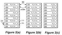
ブロック106は、ブロック104のn型クラッド層上のAlInNまたはAlInGaN活性領域の成長を表す。所望のn型AlInNまたはAlInGaNのクラッド厚さを達成した時点で、より多くのインジウムをウェル領域に取り込むように、反応器の温度設定点を10℃から80℃だけ減少させる。温度が設定点に到達した時点で、AlInGaN障壁層を成長させる。所望の厚さを達成した時点で、AlInNまたはAlInGaN活性層の所望の組成を得るように、第III族源の流速またはNH3の流速を増大または減少させることができる。活性層(例えば、井戸層)を所望の厚さに成長させた後、通常は3nmから10nmである障壁を頂部に成長させる。これは、SQWを形成する。例えば、AlInN(活性井戸層)/AlInGaN(障壁)またはAlInGaN(活性層)/AlInGaN(障壁)を成長させてもよく、また、MQWを形成するようにこの構造を繰り返すことができる。インジウム組成は、所望のλpeakを達成するように、10%から30%の範囲であり得る。可能なMQW構造を図2に示す。
図2(a)、2(b)、および2(c)は、ブロック104で成長させた第1のAlxIn1−xNまたはAlyInzGa1−y−zN層の無極性または半極性面上に、第1のAlxIn1−xNまたはAlyInzGa1−y−zN量子井戸障壁層200として、AlxIn1−xNまたはAlyInzGa1−y−zN層のうちの1つをエピタキシャルに成長させるステップと;第1のAlxIn1−xNまたはAlyInzGa1−y−zN量子井戸障壁層200の無極性または半極性面204上に、かつ360nm未満のピーク波長を有するエレクトロルミネセンスを放射する厚さ206および(Al、In、Ga)N組成に、AlyInzGa1−y−zNまたはAlxIn1−xN量子井戸層202として、AlxIn1−xNまたはAlyInzGa1−y−zN層のうちの1つをエピタキシャルに成長させるステップと;AlxIn1−xNまたはAlyInzGa1−y−zN量子井戸層202の無極性または半極性面210上に、第2のAlxIn1−xNまたはAlyInzGa1−y−zN量子井戸障壁層208として、AlxIn1−xNまたはAlyInzGa1−y−zN層のうちの1つをエピタキシャルに成長させるステップであって、それによって、第1のAlyInzGa1−y−zNまたはAlxIn1−xN量子井戸障壁層200と、第2のAlyInzGa1−y−zNまたはAlxIn1−xN量子井戸障壁層208との間に、AlxIn1−xNまたはAlyInzGa1−y−zN量子井戸層202を備える量子井戸構造を形成する、ステップを示す。図2(a)−(c)において、構造は、4周期を有するMQWを形成するように繰り返される。
2 (a), 2 (b), and 2 (c) show the nonpolarity of the first Al x In 1-x N or Al y In z Ga 1-yz N layer grown in
図2(a)の実施例において、第1の量子井戸障壁層200および第2の量子井戸障壁層208はどちらも、AlyInzGa1−y−zNであり、量子井戸202は、AlxIn1−xNである。図2(b)の実施例において、第1の量子井戸障壁層200および第2の量子井戸障壁層208はどちらも、AlyInzGa1−y−zNであり、量子井戸202は、障壁層200、208とは異なる組成(例えば、Aly’Inz’Ga1−y’−z’N)を伴う、AlyInzGa1−y−zNである。図2(c)の実施例において、第1の量子井戸障壁層200および第2の量子井戸障壁層208はどちらも、AlyGa1−yNであり、量子井戸202は、AlxIn1−xNである。例えば、AlxIn1−xNおよびAlyInzGa1−y−zN層202のうちの少なくとも1つを、10%から30%の範囲のインジウム組成を伴う発光デバイスとして成長させてもよい。
In the example of FIG. 2A, both the first quantum
ブロック108は、ブロック106で成長させた活性領域上に、電子阻止層(EBL)を成長させるステップであって、EBLの中の第III族種の組成は、EBLと障壁との間で所望の伝導体オフセットを得るように調整される、ステップを表す。
ブロック110は、ブロック108で成長させたEBL層上に、p型AlInNまたはAlInGaNクラッド層を成長させるステップを表す。所望のEBL厚さを達成した時点で、反応器の設定点温度を10℃から80℃だけ増大させる。次いで、p型AlInNまたはAlInGaN層を達成するように、Cp2Mgを反応器の中に導入する。p型合金の組成は、n型合金の組成と同じである。したがって、ブロック110は、AlxIn1−xNまたはAlyInzGa1−y−zN層のうちの1つを、第2の導電型を有するAlxIn1−xNまたはAlyInzGa1−y−zN層として、ブロック108のEBLおよびブロック106の量子井戸構造上にエピタキシャルに成長させる実施例を示す。
次いで、ブロック112に表されるように、ブロック110で成長させたp型クラッド層上に、p型GaN接触層を成長させる。例えば、接触層を形成するように、薄くかつ高度にマグネシウム(Mg)ドープしたp型GaN層を頂部に成長させてもよい。
Next, as represented by
反応器を冷却した時点で、ブロック114に表されるように、ブロック112で成長させたp型GaN接触層(Mgドープ層)を活性化するために、窒化物デバイス(ブロック110−112で形成される)を備えるエピタキシャルウエハを除去して、700℃で15分間、水素欠乏雰囲気の中で焼鈍する。
Upon cooling of the reactor, a nitride device (formed at block 110-112) is activated to activate the p-type GaN contact layer (Mg doped layer) grown at
次のステップでは、デバイスを製造する。ここでは、UV LEDのためのプロセスを実施例として説明する。エピタキシャルウエハを焼鈍した時点で、ブロック116(ブロック114で活性化したp−GaN層上に、p型接触層をパターン化する)に表されるように、p型接触(p−接触)をウエハ上にパターン化するために、フォトリソグラフィ技術を使用する。次いで、ブロック118(p−接触金属を、ブロック116でパターン化したパターン化p型GaN層上に蒸着して合金化する)に表されるように、金属合金を形成するように、p接触金属(20Å〜100ÅのNi/Au)を、電子ビーム蒸着器によって蒸着して、1〜10分間、N2またはN2/O2雰囲気下で焼鈍する。次いで、ブロック120(ブロック114−118の結果によって生じるp型GaN接触層を部分的に除去する)に表されるように、p−GaN接触層を、ドライエッチング技術によって少なくとも部分的に除去する。ブロック120のステップでは、図3に示されるように、ブロック114−118の結果によって生じる光吸収GaN層を除去し、ブロック110で成長させたp型クラッド層を露出させる。このステップの後、ブロック122に表されるように、ドライエッチングによって、ブロック100−120の結果として生じる構造の中にメサを形成し、エッチングでブロック104のn型クラッド層を露出させる。次いで、ブロック124(n型接触金属を、ブロック104で成長させ。ブロック122で露出させたn型クラッド層上に蒸着して合金化する)に表されるように、金属合金を形成するように、n型接触金属(Ti/Al/Ni/Au)を蒸着して、1〜10分間、N2またはN2/O2雰囲気下で焼鈍する。次いで、ブロック126(ブロック118の合金化p−接触金属およびブロック124の合金化n−接触金属上に、それぞれ、接触パッド用の金属を蒸着する)によって表されるように、接触パッド用の金属を、電子ビーム蒸着器を使用して蒸着する。
The next step is to manufacture the device. Here, the process for UV LEDs is described as an example. When the epitaxial wafer is annealed, the p-type contact (p-contact) is represented in block 116 (patterning the p-type contact layer on the p-GaN layer activated in block 114). Photolithographic techniques are used to pattern the top. The p-contact metal is then formed to form a metal alloy as represented by block 118 (p-contact metal is deposited and alloyed onto the patterned p-type GaN layer patterned at block 116). (20 to 100% Ni / Au) is deposited by an electron beam evaporator and annealed for 1 to 10 minutes in an N 2 or N 2 / O 2 atmosphere. The p-GaN contact layer is then at least partially removed by dry etching techniques, as represented by block 120 (partially removing the p-type GaN contact layer resulting from blocks 114-118). In the step of
次いで、ブロック128(基板を除去する)によって表されるように、典型的に、ブロック100の基板を除去する。最後に、典型的に、フリップチップパッケージングを実施し、典型的に、鏡面反射器を、ブロック128の基板除去によって露出したデバイス側に蒸着する。
The substrate of
図3は、無極性または半極性GaN基板310上に製造した(例えば、成長させた)、0≦y≦1、0≦z≦1、および0≦y+z≦1である、1つ以上のAlxIn1−xNまたはAlyInzGa1−y−zN層302、304、306、および308を備える(例えば、ブロック104、106、108、および110で示される)、前述のステップを実施した後に得られる、最終的な光電子デバイス300(例えば、LEDまたはLD)の構造の実施例を示し、図中、AlxIn1−xNまたはAlyInzGa1−y−zN層302、304、306、および308は、無極性または半極性である(すなわち、層302、304、306、および308の成長表面が、III族窒化物の無極性面(例えば、m面またはa面)または半極性面であるように、無極性または半極性方向に成長させる)。
FIG. 3 illustrates one or more Al fabricated on (eg, grown) on a nonpolar or
全ての層302、304、306、および308は、少なくともいくらかのインジウムを含有する。AlxIn1−xNまたはAlyInzGa1−y−zN層302、304、306、および308は、例えば、少なくともAl、In、およびNを含み得る。
All
例えば、AlxIn1−xNまたはAlyInzGa1−y−zN層のうちの1つ以上は、無極性または半極性GaN基板310に密接に格子整合され(例えば、無極性または半極性GaN基板310上のAlxIn1−xNまたはAlyInzGa1−y−zNに基づくn型クラッド層302)、AlxIn1−xNまたはAlyInzGa1−y−zN層のうちの1つ以上は、n型伝導性のためにSiでドープされ(例えば、シリコンでドープされる、n型クラッド層302)、AlxIn1−xNまたはAlyInzGa1−y−zN層のうちの1つ以上は、p型伝導性のためにMgでドープされ(Mgでドープされる、p型クラッド層308)、複数のAlxIn1−xNまたはAlyInzGa1−y−zN層302、304、306、および308は、1つ以上のヘテロ構造または1つ以上の量子井戸ヘテロ構造304(例えば、n型クラッド層302上の、AlxIn1−xNまたはAlyInzGa1−y−zN基づくSQWまたはMQW304)を形成する。一実施例において、AlxIn1−xNまたはAlyInzGa1−y−zN層304のうちの1つ以上のインジウム組成は、10%から30%の範囲である。
For example, one or more of the Al x In 1-x N or Al y In z Ga 1-yz N layers are closely lattice matched to the nonpolar or semipolar GaN substrate 310 (eg, nonpolar or on semipolar GaN substrate 310 Al x in 1-x n or Al y in z Ga 1-y -z n based on n-type cladding layer 302), Al x in 1- x n or Al y in z Ga 1- One or more of the yz N layers are doped with Si for n-type conductivity (eg, n-
図3のデバイス300はさらに、量子井戸層304上に、AlxIn1−xNまたはAlyInzGa1−y−zNに基づく電子阻止層(EBL)306を備える。AlxIn1−xNまたはAlyInzGa1−y−zNに基づくp型クラッド層308は、1つ以上のEBL306上にある。また、p型クラッド層308上のp++GaN接触層312、p++GaN接触層312に対する金属接触314、およびn型クラッド層302に対する金属接触316も示される。
The
層302は、典型的に、基板に密接に格子整合される。「密接に格子整合した」とは、成長した厚さにおいていかなる膜の緩和もないこととほぼ同じである。いかなる緩和もないことは、基板310からの転位以外の他の転位がないことを意味する。
したがって、図2(a)、2(b)、2(c)、および3は、無極性または半極性GaN基板310上に成長させられる、少なくともAl、In、およびNを含有する1つ以上の発光層202、304を備える、光電子デバイス300を示し、図中、発光層202、304は、無極性または半極性層である。
Accordingly, FIGS. 2 (a), 2 (b), 2 (c), and 3 are grown on a nonpolar or
図2(a)、2(b)、2(c)、および3はまた、第1の導電型(例えば、n型であるが、これに限定されない)を有する第1の(Al、In、Ga)N層302;第2の導電型(例えば、p型であるが、これに限定されない)を有する第2の(Al、In、Ga)N層308;および、第1の(Al、In、Ga)N量子井戸障壁層200の無極性または半極性面204上にエピタキシャルに成長させられる、(Al、In、Ga)N量子井戸層202と、(Al、In、Ga)N量子井戸層202の無極性または半極性面210上にエピタキシャルに成長させられる、第2の(Al、In、Ga)N量子井戸障壁層208とを備える、(Al、In、Ga)N量子井戸構造304を示し、(1)図中、量子井戸構造304は、(Al、In、Ga)N量子井戸構造304が、第1の(Al、In、Ga)N層302と第2の(Al、In、Ga)N層308との間にあるように、(Al、In、Ga)N層(例えば、第1の(Al、In、Ga)N層302)の無極性または半極性面318上にエピタキシャルに成長させられ、量子井戸202は、360nm未満のピーク波長を有するエレクトロルミネセンスを放射する、厚さ206および(Al、In、Ga)N組成を有する。例えば、デバイス300は、280nmから360nmの範囲のピーク放射波長を有する、発光デバイスであり得る。
FIGS. 2 (a), 2 (b), 2 (c), and 3 also have a first (Al, In,) having a first conductivity type (eg, but not limited to n-type). Ga)
(Al、In、Ga)N層302は、典型的に、基板310の無極性または半極性面320上に成長させられる。続いて基板310が除去された後であっても(例えば、図1のブロック128を参照のこと)、層302は、GaN上のエピタキシャル成長と関連する転位密度を保持する。その結果、(Al、In、Ga)N量子井戸構造304は、(Al、In、Ga)N層302上にエピタキシャルに成長させられ、(Al、In、Ga)N層302は、基板310が除去された後であっても、GaN(例えば、基板310)上にエピタキシャルに成長させられ、かつそれに密接に格子整合される、(Al、In、Ga)N層の低転位密度を有する。(Al、In、Ga)N層302は、106cm−2未満の転位密度を有し得、(Al、In、Ga)N層302(および/または層302と基板310との間の層、および/または層304、306、および308)は、横方向エピタキシャル過成長を含まない。
The (Al, In, Ga)
(Al、In、Ga)Nの十分に低い転位密度および比較的に高いインジウム組成により、活性領域(発光領域)304は、15%を超える発光デバイス300のIQEを達成することができ、これは、10%未満のインジウム含有量(y)を伴うAlxInyGa1−x−yN合金によって得られる値であった。したがって、1%を超える発光デバイス300の外部量子効率を達成することが可能である。
With a sufficiently low dislocation density and relatively high indium composition of (Al, In, Ga) N, the active region (light emitting region) 304 can achieve an IQE of the
概して、エッジ型転位および螺旋型転位等の転位は、非放射再結合場所を提供するトラップであることが公知である。転位が多くなることは、非放射再結合が多くなり、したがってIQEが低くなることを意味する。したがって、外部量子効率は、低下する(外部量子効率=IQE×抽出効率)。 In general, dislocations such as edge-type dislocations and screw-type dislocations are known to be traps that provide non-radiative recombination sites. More dislocations means more non-radiative recombination and thus lower IQE. Therefore, the external quantum efficiency decreases (external quantum efficiency = IQE × extraction efficiency).
製造プロセスの詳細は、レーザダイオード等の他のUV放出デバイスのために改良する必要がある。 The details of the manufacturing process need to be improved for other UV emitting devices such as laser diodes.
本発明の有用性を高めるために、デバイスを、最小の可能な転位を有するバルクGaN基板上に成長させることが重要である。バルクGaN基板は、本質的に、自立型である厚いGaNである。一実施例は、サファイア上に成長させられる厚い(約300μm)GaNであり、次いで、サファイア基板からリフトオフされる。 In order to increase the usefulness of the present invention, it is important to grow the device on a bulk GaN substrate with the smallest possible dislocations. Bulk GaN substrates are essentially thick GaN that is free-standing. One example is thick (about 300 μm) GaN grown on sapphire and then lifted off from the sapphire substrate.
しかしながら、GaN基板は、360nmより低い放射波長に対する吸収層である。したがって、ブロック128に表されるように、光抽出を向上させるように、GaN基板を除去することが必要である。GaN基板は、ラッピング、研摩、およびドライエッチングプロセスによって除去することができる。よって、鏡面反射器を伴うフリップチップパッケージング(ブロック130に表される)は、前述のLED等の発光デバイスからの光抽出を最大化することができる。
However, the GaN substrate is an absorption layer for radiation wavelengths lower than 360 nm. Therefore, as represented by
(可能な変形例)
前述のデバイスに対する成長仕様は、MOCVDによる無極性および半極性AlInNおよびAlInGaN層のヘテロエピタキシャル成長を利用したが、本発明は、あらゆる成長技術を使用することができる。例えば、無極性および半極性AlInNおよびAlInGaNはまた、適切な成長条件を伴う分子ビームエピタキシ(MBE)によって成長させられ得る。
(Possible variations)
Although the growth specifications for the aforementioned devices utilized heteroepitaxial growth of nonpolar and semipolar AlInN and AlInGaN layers by MOCVD, the present invention can use any growth technique. For example, nonpolar and semipolar AlInN and AlInGaN can also be grown by molecular beam epitaxy (MBE) with appropriate growth conditions.
GaN基板を除去するために、ドライエッチング技術を使用する代わりに、n型クラッド層の成長の前に、非常に薄いInGaN層を蒸着することができる。デバイスを成長させた後、InGaN層は、UV光源を使用する光電気化学(PEC)エッチングによってエッチングで除去することができる。 Instead of using a dry etching technique to remove the GaN substrate, a very thin InGaN layer can be deposited prior to the growth of the n-type cladding layer. After growing the device, the InGaN layer can be etched away by photoelectrochemical (PEC) etching using a UV light source.
前述の成長プロセスは、単に事前の実験に基づく1つの一組の可能な成長条件に過ぎない。無極性および半極性AlInNおよびAlInGaN層を成長させるために、ガス流、成長圧力、および成長温度等の成長条件をさらに調査することができる。AlInNの成長に関するさらなる情報は、[6]に見出すことができる。 The aforementioned growth process is just one set of possible growth conditions based on prior experiments. Growth conditions such as gas flow, growth pressure, and growth temperature can be further investigated to grow nonpolar and semipolar AlInN and AlInGaN layers. More information on the growth of AlInN can be found in [6].
(利点および改良点)
既存の実行法は、表面がGa(Al)面またはかN面である、c面サファイアまたはSiC基板上に、AlGaNに基づくUV放出デバイスを成長させるものである。c方向に垂直な面は、大きい電気陰性度差のため、自発分極を有する。したがって、異なる分極の多層間の界面は、本質的に分極電荷を構築して、内部電場をもたらす。この電場は、活性層等の薄い層に対してかなり大きくなる可能性があり、エネルギー帯構造を変化させる。基板と後続の層(AlNおよびAlGaN)との間の格子不整合は、圧電分極を導入し、帯域構造をさらに変化させ得る。
(Advantages and improvements)
An existing practice is to grow AlGaN-based UV emitting devices on c-plane sapphire or SiC substrates with a Ga (Al) or N-face surface. The plane perpendicular to the c direction has spontaneous polarization due to a large difference in electronegativity. Thus, the interface between multiple layers of different polarization essentially builds up a polarization charge resulting in an internal electric field. This electric field can be quite large for thin layers such as the active layer, changing the energy band structure. Lattice mismatch between the substrate and subsequent layers (AlN and AlGaN) can introduce piezoelectric polarization and further change the band structure.
本発明は、自発および圧電の両方の分極を最小化したデバイス構造を説明する。自発分極は、無極性または半極性結晶配向のデバイスを成長させることによって減少する。さらに重要なことに、圧電分極の低減は、GaN基板に密接に格子整合されるAlInNまたはAlInGaNクラッド層を成長させることによって達成される。量子井戸層だけが、わずかに圧縮歪みを受ける。格子整合状態はまた、クラッド層と基板との間の界面から生じるいかなる付加的な転位もないことを意味する。したがって、QCSE効果および転位密度の両方の低減は、より高いIQEをもたらす。改良された結晶品質はまた、UV領域における高出力および高効率のLDを実現できることを意味する。無極性および半極性バルクGaN基板が、高い結晶品質で利用可能であるので、本発明で説明される新しい構造は、現在利用可能である最先端技術のUV放出デバイスよりも効率的であることが予期される。 The present invention describes a device structure that minimizes both spontaneous and piezoelectric polarization. Spontaneous polarization is reduced by growing nonpolar or semipolar crystal orientation devices. More importantly, the reduction of piezoelectric polarization is achieved by growing an AlInN or AlInGaN cladding layer that is closely lattice matched to the GaN substrate. Only the quantum well layer undergoes a slight compressive strain. The lattice matched state also means that there are no additional dislocations arising from the interface between the cladding layer and the substrate. Thus, a reduction in both the QCSE effect and the dislocation density results in higher IQE. Improved crystal quality also means that high power and high efficiency LD in the UV region can be realized. Because nonpolar and semipolar bulk GaN substrates are available with high crystal quality, the new structure described in the present invention may be more efficient than state-of-the-art UV emitting devices currently available. Expected.

これは、本発明の好適な実施形態の説明を締めくくるものである。本発明の1つ以上の実施形態の上述の説明は、図解および説明のために示したものである。本記述は、網羅的であること、または本発明を開示された形態に限定することを意図したものではない。上述の教示に照らして、多数の修正および変形が可能である。本発明の範囲は、この詳細な説明によって限定されるのではなく、むしろ本明細書に添付された請求項によって限定されることを意図する。
This concludes the description of the preferred embodiment of the present invention. The foregoing description of one or more embodiments of the invention has been presented for purposes of illustration and description. This description is not intended to be exhaustive or to limit the invention to the form disclosed. Many modifications and variations are possible in light of the above teaching. It is intended that the scope of the invention be limited not by this detailed description, but rather by the claims appended hereto.
Claims (20)
(a)前記無極性または半極性GaN基板上の、AlxIn1−xNまたはAlyInzGa1−y−zNに基づくn型クラッド層と、
(b)該n型クラッド層上の、AlxIn1−xNまたはAlyInzGa1−y−zNに基づく単一量子井戸または多重量子井戸を備える、前記発光層と、
(c)該量子井戸上の、1つ以上のAlxIn1−xNまたはAlyInzGa1−y−zNに基づく電子阻止層と、
(d)該電子阻止層上の、AlxIn1−xNまたはAlyInzGa1−y−zNに基づくp型クラッド層と
をさらに備え、
(e)該AlxIn1−xNまたはAlyInzGa1−y−zN層(a)、(b)、(c)、および(d)は、無極性または半極性であり、0≦y≦1、0≦z≦1、および0≦y+z≦1である、請求項1に記載のデバイス。 The device is a light emitting device, and the light emitting device comprises:
(A) an n-type cladding layer based on Al x In 1-x N or Al y In z Ga 1- yz N on the nonpolar or semipolar GaN substrate;
(B) the light emitting layer comprising a single quantum well or multiple quantum wells based on Al x In 1-x N or Al y In z Ga 1- yz N on the n-type cladding layer;
(C) on the quantum well, an electron blocking layer based on one or more Al x In 1-x N or Al y In z Ga 1-y -z N,
(D) further comprising a p-type cladding layer based on Al x In 1-x N or Al y In z Ga 1- yz N on the electron blocking layer,
(E) the Al x In 1-x N or Al y In z Ga 1-yz N layer (a), (b), (c), and (d) is nonpolar or semipolar; The device of claim 1, wherein 0 ≦ y ≦ 1, 0 ≦ z ≦ 1, and 0 ≦ y + z ≦ 1.
(b)第2の導電型を有する、第2の(Al、In、Ga)N層と、
(c)第1の(Al、In、Ga)N量子井戸障壁層の無極性または半極性面上にエピタキシャルに成長させられる、(Al、In、Ga)N量子井戸層と、該(Al、In、Ga)N量子井戸層の無極性または半極性面上にエピタキシャルに成長させられる、第2の(Al、In、Ga)N量子井戸障壁層とを備える、(Al、In、Ga)N量子井戸構造と
を備え、
(1)該量子井戸構造は、該(Al、In、Ga)N量子井戸構造が、該第1の(Al、In、Ga)N層と該第2の(Al、In、Ga)N層との間にあるように、該第1の(Al、In、Ga)N層の無極性または半極性面上にエピタキシャルに成長させられ、
(2)該量子井戸は、360nm未満のピーク波長を有するエレクトロルミネセンスを放射する、厚さおよび(Al、In、Ga)N組成を有する、
光電子デバイス。 (A) a first (Al, In, Ga) N layer having a first conductivity type;
(B) a second (Al, In, Ga) N layer having a second conductivity type;
(C) an (Al, In, Ga) N quantum well layer epitaxially grown on a nonpolar or semipolar surface of the first (Al, In, Ga) N quantum well barrier layer; (Al, In, Ga) N comprising a second (Al, In, Ga) N quantum well barrier layer grown epitaxially on a nonpolar or semipolar surface of the In, Ga) N quantum well layer With quantum well structure,
(1) The quantum well structure includes the (Al, In, Ga) N quantum well structure, the first (Al, In, Ga) N layer, and the second (Al, In, Ga) N layer. And epitaxially grown on a nonpolar or semipolar surface of the first (Al, In, Ga) N layer,
(2) the quantum well has a thickness and (Al, In, Ga) N composition that emits electroluminescence having a peak wavelength of less than 360 nm;
Optoelectronic device.
(Al、In、Ga)N層の無極性または半極性面上にエピタキシャルに成長させられる(Al、In、Ga)N量子井戸構造と、
十分に低い該(Al、In、Ga)N層の転位密度と
をさらに備え、該無極性または半極性面および該転位密度は、15%よりも大きい該発光デバイスの内部量子効率、および1%よりも大きい該発光デバイスの外部量子効率を達成する、請求項13に記載のデバイス。 The device is a light emitting device;
An (Al, In, Ga) N quantum well structure that is epitaxially grown on a nonpolar or semipolar surface of the (Al, In, Ga) N layer;
And a dislocation density of the (Al, In, Ga) N layer that is sufficiently low, the nonpolar or semipolar plane and the dislocation density being greater than 15%, 14. The device of claim 13, wherein the device achieves an external quantum efficiency of the light emitting device that is greater than.
該第1のAlxIn1−xNまたはAlyInzGa1−y−zN層の無極性または半極性面上に、第1のAlxIn1−xNまたはAlyInzGa1−y−zN量子井戸障壁層として、AlxIn1−xNまたはAlyInzGa1−y−zN層のうちの1つを、エピタキシャルに成長させるステップと、
該第1のAlxIn1−xNまたはAlyInzGa1−y−zN量子井戸障壁層の無極性または半極性面上に、かつ360nm未満のピーク波長を有するエレクトロルミネセンスを放射する厚さおよび(Al、In、Ga)N組成に、AlxIn1−xNまたはAlyInzGa1−y−zN量子井戸層として、AlxIn1−xNまたはAlyInzGa1−y−zN層のうちの1つをエピタキシャルに成長させるステップと、
該AlxIn1−xNまたはAlyInzGa1−y−zN量子井戸層の無極性または半極性面上に、第2のAlxIn1−xNまたはAlyInzGa1−y−zN量子井戸障壁層として、AlxIn1−xNまたはAlyInzGa1−y−zN層のうちの1つをエピタキシャルに成長させるステップであって、それによって、該第1のAlxIn1−xNまたはAlyInzGa1−y−zN量子井戸障壁層と、該第2のAlxIn1−xNまたはAlyInzGa1−y−zN量子井戸障壁層との間に、該AlxIn1−xNまたはAlyInzGa1−y−zN量子井戸層を備える量子井戸構造を形成する、ステップと、
第2の導電型を有する第2のAlxIn1−xNまたはAlyInzGa1−y−zN層として、該量子井戸構造上に、AlxIn1−xNまたはAlyInzGa1−y−zN層のうちの1つをエピタキシャルに成長させるステップであって、前記発光活性層は、該量子井戸層を備える、ステップと
をさらに含む、請求項17に記載の方法。 On the nonpolar or semipolar surface of the GaN substrate such that the first Al x In 1-x N or Al y In z Ga 1-yz N layer is closely lattice matched to the GaN substrate As the first Al x In 1-x N or Al y In z Ga 1-yz N layer having the first conductivity type, Al x In 1-x N or Al y In z Ga 1-y- epitaxially growing one of the z N layers;
On the nonpolar or semipolar plane of the first Al x In 1-x N or Al y In z Ga 1-yz N layer, the first Al x In 1-x N or Al y In z Ga Epitaxially growing one of an Al x In 1-x N or Al y In z Ga 1-yz N layer as a 1 -yz N quantum well barrier layer;
On non-polar or semi-polar surfaces of the first Al x In 1-x N or Al y In z Ga 1-y -z N quantum well barrier layer, and emit electroluminescence having a peak wavelength of less than 360nm As the Al x In 1-x N or Al y In z Ga 1-yz N quantum well layer, the Al x In 1-x N or Al y In epitaxially growing one of the z Ga 1-yz N layers;
The Al x In 1-x N or Al y In z Ga 1-y -z in N on nonpolar or semipolar surface of the quantum well layer, a second Al x In 1-x N or Al y In z Ga 1 as -y-z N quantum well barrier layer, a step of growing one of Al x in 1-x N or Al y in z Ga 1-y -z N layer epitaxially, whereby the A first Al x In 1-x N or Al y In z Ga 1-yz N quantum well barrier layer and the second Al x In 1-x N or Al y In z Ga 1-yz Forming a quantum well structure comprising the Al x In 1-x N or Al y In z Ga 1-yz N quantum well layer with the N quantum well barrier layer;
As a second Al x In 1-x N or Al y In z Ga 1-y -z N layer having a second conductivity type, on the quantum well structure, Al x In 1-x N or Al y an In one of the z Ga 1-y-z N layer a step of growing epitaxially the light emitting active layer includes a quantum well layer, further comprising the steps, the method according to claim 17 .
Applications Claiming Priority (3)
| Application Number | Priority Date | Filing Date | Title |
|---|---|---|---|
| US11044908P | 2008-10-31 | 2008-10-31 | |
| US61/110,449 | 2008-10-31 | ||
| PCT/US2009/062982 WO2010051537A1 (en) | 2008-10-31 | 2009-11-02 | Optoelectronic device based on non-polar and semi-polar aluminum indium nitride and aluminum indium gallium nitride alloys |
Publications (2)
| Publication Number | Publication Date |
|---|---|
| JP2012507874A true JP2012507874A (en) | 2012-03-29 |
| JP2012507874A5 JP2012507874A5 (en) | 2012-12-20 |
Family
ID=42129326
Family Applications (1)
| Application Number | Title | Priority Date | Filing Date |
|---|---|---|---|
| JP2011534857A Pending JP2012507874A (en) | 2008-10-31 | 2009-11-02 | Optoelectronic devices based on nonpolar or semipolar AlInN and AlInGaN alloys |
Country Status (3)
| Country | Link |
|---|---|
| US (3) | US8084763B2 (en) |
| JP (1) | JP2012507874A (en) |
| WO (1) | WO2010051537A1 (en) |
Cited By (2)
| Publication number | Priority date | Publication date | Assignee | Title |
|---|---|---|---|---|
| JP2011003661A (en) * | 2009-06-17 | 2011-01-06 | Rohm Co Ltd | Semiconductor laser element |
| JP2021027193A (en) * | 2019-08-06 | 2021-02-22 | 日機装株式会社 | Manufacturing method of nitride semiconductor light-emitting device |
Families Citing this family (101)
| Publication number | Priority date | Publication date | Assignee | Title |
|---|---|---|---|---|
| US7842527B2 (en) | 2006-12-11 | 2010-11-30 | The Regents Of The University Of California | Metalorganic chemical vapor deposition (MOCVD) growth of high performance non-polar III-nitride optical devices |
| JP5743127B2 (en) | 2005-06-01 | 2015-07-01 | ザ リージェンツ オブ ザ ユニバーシティ オブ カリフォルニア | Method and apparatus for growth and fabrication of semipolar (Ga, Al, In, B) N thin films, heterostructures and devices |
| TWI492411B (en) * | 2006-12-11 | 2015-07-11 | Univ California | Non-polar and semi-polar light emitting devices |
| US8871024B2 (en) * | 2008-06-05 | 2014-10-28 | Soraa, Inc. | High pressure apparatus and method for nitride crystal growth |
| US8097081B2 (en) | 2008-06-05 | 2012-01-17 | Soraa, Inc. | High pressure apparatus and method for nitride crystal growth |
| US20090301388A1 (en) * | 2008-06-05 | 2009-12-10 | Soraa Inc. | Capsule for high pressure processing and method of use for supercritical fluids |
| US9157167B1 (en) | 2008-06-05 | 2015-10-13 | Soraa, Inc. | High pressure apparatus and method for nitride crystal growth |
| US9404197B2 (en) | 2008-07-07 | 2016-08-02 | Soraa, Inc. | Large area, low-defect gallium-containing nitride crystals, method of making, and method of use |
| US8430958B2 (en) * | 2008-08-07 | 2013-04-30 | Soraa, Inc. | Apparatus and method for seed crystal utilization in large-scale manufacturing of gallium nitride |
| US8021481B2 (en) | 2008-08-07 | 2011-09-20 | Soraa, Inc. | Process and apparatus for large-scale manufacturing of bulk monocrystalline gallium-containing nitride |
| US8979999B2 (en) | 2008-08-07 | 2015-03-17 | Soraa, Inc. | Process for large-scale ammonothermal manufacturing of gallium nitride boules |
| US10036099B2 (en) | 2008-08-07 | 2018-07-31 | Slt Technologies, Inc. | Process for large-scale ammonothermal manufacturing of gallium nitride boules |
| US7976630B2 (en) | 2008-09-11 | 2011-07-12 | Soraa, Inc. | Large-area seed for ammonothermal growth of bulk gallium nitride and method of manufacture |
| US20100295088A1 (en) * | 2008-10-02 | 2010-11-25 | Soraa, Inc. | Textured-surface light emitting diode and method of manufacture |
| US8354679B1 (en) | 2008-10-02 | 2013-01-15 | Soraa, Inc. | Microcavity light emitting diode method of manufacture |
| US8455894B1 (en) | 2008-10-17 | 2013-06-04 | Soraa, Inc. | Photonic-crystal light emitting diode and method of manufacture |
| WO2010051537A1 (en) | 2008-10-31 | 2010-05-06 | The Regents Of The University Of California | Optoelectronic device based on non-polar and semi-polar aluminum indium nitride and aluminum indium gallium nitride alloys |
| KR101139142B1 (en) | 2008-11-06 | 2012-04-26 | 파나소닉 주식회사 | Nitride semiconductor element and method for manufacturing the same |
| US9543392B1 (en) | 2008-12-12 | 2017-01-10 | Soraa, Inc. | Transparent group III metal nitride and method of manufacture |
| US8987156B2 (en) | 2008-12-12 | 2015-03-24 | Soraa, Inc. | Polycrystalline group III metal nitride with getter and method of making |
| US8461071B2 (en) * | 2008-12-12 | 2013-06-11 | Soraa, Inc. | Polycrystalline group III metal nitride with getter and method of making |
| US9589792B2 (en) | 2012-11-26 | 2017-03-07 | Soraa, Inc. | High quality group-III metal nitride crystals, methods of making, and methods of use |
| USRE47114E1 (en) | 2008-12-12 | 2018-11-06 | Slt Technologies, Inc. | Polycrystalline group III metal nitride with getter and method of making |
| US8878230B2 (en) * | 2010-03-11 | 2014-11-04 | Soraa, Inc. | Semi-insulating group III metal nitride and method of manufacture |
| US20110100291A1 (en) * | 2009-01-29 | 2011-05-05 | Soraa, Inc. | Plant and method for large-scale ammonothermal manufacturing of gallium nitride boules |
| US8247886B1 (en) | 2009-03-09 | 2012-08-21 | Soraa, Inc. | Polarization direction of optical devices using selected spatial configurations |
| CN102067348B (en) * | 2009-04-06 | 2013-03-27 | 松下电器产业株式会社 | Nitride semiconductor element and method for production thereof |
| US8299473B1 (en) | 2009-04-07 | 2012-10-30 | Soraa, Inc. | Polarized white light devices using non-polar or semipolar gallium containing materials and transparent phosphors |
| JP5143076B2 (en) * | 2009-04-09 | 2013-02-13 | シャープ株式会社 | Manufacturing method of nitride semiconductor light emitting device |
| US8791499B1 (en) | 2009-05-27 | 2014-07-29 | Soraa, Inc. | GaN containing optical devices and method with ESD stability |
| US9800017B1 (en) | 2009-05-29 | 2017-10-24 | Soraa Laser Diode, Inc. | Laser device and method for a vehicle |
| US9250044B1 (en) | 2009-05-29 | 2016-02-02 | Soraa Laser Diode, Inc. | Gallium and nitrogen containing laser diode dazzling devices and methods of use |
| US8509275B1 (en) | 2009-05-29 | 2013-08-13 | Soraa, Inc. | Gallium nitride based laser dazzling device and method |
| US9000466B1 (en) | 2010-08-23 | 2015-04-07 | Soraa, Inc. | Methods and devices for light extraction from a group III-nitride volumetric LED using surface and sidewall roughening |
| WO2011035265A1 (en) | 2009-09-18 | 2011-03-24 | Soraa, Inc. | Power light emitting diode and method with current density operation |
| US9293644B2 (en) | 2009-09-18 | 2016-03-22 | Soraa, Inc. | Power light emitting diode and method with uniform current density operation |
| US9583678B2 (en) | 2009-09-18 | 2017-02-28 | Soraa, Inc. | High-performance LED fabrication |
| US8435347B2 (en) | 2009-09-29 | 2013-05-07 | Soraa, Inc. | High pressure apparatus with stackable rings |
| US9175418B2 (en) | 2009-10-09 | 2015-11-03 | Soraa, Inc. | Method for synthesis of high quality large area bulk gallium based crystals |
| WO2011077704A1 (en) * | 2009-12-25 | 2011-06-30 | パナソニック株式会社 | Nitride semiconductor element and method for manufacturing same |
| JP5589380B2 (en) * | 2009-12-28 | 2014-09-17 | 日亜化学工業株式会社 | Nitride semiconductor device |
| US8740413B1 (en) | 2010-02-03 | 2014-06-03 | Soraa, Inc. | System and method for providing color light sources in proximity to predetermined wavelength conversion structures |
| US20110186874A1 (en) * | 2010-02-03 | 2011-08-04 | Soraa, Inc. | White Light Apparatus and Method |
| US8905588B2 (en) | 2010-02-03 | 2014-12-09 | Sorra, Inc. | System and method for providing color light sources in proximity to predetermined wavelength conversion structures |
| US10147850B1 (en) | 2010-02-03 | 2018-12-04 | Soraa, Inc. | System and method for providing color light sources in proximity to predetermined wavelength conversion structures |
| WO2011102411A1 (en) * | 2010-02-19 | 2011-08-25 | シャープ株式会社 | Nitride semiconductor light-emitting element and method for producing same |
| US20110233521A1 (en) * | 2010-03-24 | 2011-09-29 | Cree, Inc. | Semiconductor with contoured structure |
| US9450143B2 (en) | 2010-06-18 | 2016-09-20 | Soraa, Inc. | Gallium and nitrogen containing triangular or diamond-shaped configuration for optical devices |
| US9564320B2 (en) | 2010-06-18 | 2017-02-07 | Soraa, Inc. | Large area nitride crystal and method for making it |
| US20120007102A1 (en) * | 2010-07-08 | 2012-01-12 | Soraa, Inc. | High Voltage Device and Method for Optical Devices |
| US8897329B2 (en) * | 2010-09-20 | 2014-11-25 | Corning Incorporated | Group III nitride-based green-laser diodes and waveguide structures thereof |
| US8729559B2 (en) * | 2010-10-13 | 2014-05-20 | Soraa, Inc. | Method of making bulk InGaN substrates and devices thereon |
| US20120126283A1 (en) * | 2010-10-27 | 2012-05-24 | The Regents Of The University Of California | High power, high efficiency and low efficiency droop iii-nitride light-emitting diodes on semipolar substrates |
| US8362458B2 (en) | 2010-12-27 | 2013-01-29 | Industrial Technology Research Institute | Nitirde semiconductor light emitting diode |
| US8786053B2 (en) | 2011-01-24 | 2014-07-22 | Soraa, Inc. | Gallium-nitride-on-handle substrate materials and devices and method of manufacture |
| US8358673B2 (en) | 2011-02-17 | 2013-01-22 | Corning Incorporated | Strain balanced laser diode |
| CN102820394B (en) * | 2011-06-07 | 2015-04-01 | 山东华光光电子有限公司 | LED structure with aluminum-component-gradient electron blocking layer |
| US8492185B1 (en) | 2011-07-14 | 2013-07-23 | Soraa, Inc. | Large area nonpolar or semipolar gallium and nitrogen containing substrate and resulting devices |
| US8686431B2 (en) | 2011-08-22 | 2014-04-01 | Soraa, Inc. | Gallium and nitrogen containing trilateral configuration for optical devices |
| DE102011112706B4 (en) | 2011-09-07 | 2021-09-02 | OSRAM Opto Semiconductors Gesellschaft mit beschränkter Haftung | Optoelectronic component |
| DE102011112713A1 (en) * | 2011-09-07 | 2013-03-07 | Osram Opto Semiconductors Gmbh | Optoelectronic component |
| US9252329B2 (en) | 2011-10-04 | 2016-02-02 | Palo Alto Research Center Incorporated | Ultraviolet light emitting devices having compressively strained light emitting layer for enhanced light extraction |
| US9694158B2 (en) | 2011-10-21 | 2017-07-04 | Ahmad Mohamad Slim | Torque for incrementally advancing a catheter during right heart catheterization |
| US10029955B1 (en) | 2011-10-24 | 2018-07-24 | Slt Technologies, Inc. | Capsule for high pressure, high temperature processing of materials and methods of use |
| US8912025B2 (en) | 2011-11-23 | 2014-12-16 | Soraa, Inc. | Method for manufacture of bright GaN LEDs using a selective removal process |
| US8482104B2 (en) | 2012-01-09 | 2013-07-09 | Soraa, Inc. | Method for growth of indium-containing nitride films |
| CN102522502B (en) * | 2012-01-10 | 2013-12-25 | 西安电子科技大学 | Terahertz GaN Gunn diode based on SiC substrate and manufacturing method thereof |
| US20130270515A1 (en) * | 2012-04-12 | 2013-10-17 | Industrial Technology Research Institute | Light emitting diode |
| WO2013134432A1 (en) * | 2012-03-06 | 2013-09-12 | Soraa, Inc. | Light emitting diodes with low refractive index material layers to reduce light guiding effects |
| US10145026B2 (en) | 2012-06-04 | 2018-12-04 | Slt Technologies, Inc. | Process for large-scale ammonothermal manufacturing of semipolar gallium nitride boules |
| JP2014027092A (en) * | 2012-07-26 | 2014-02-06 | Sharp Corp | Semiconductor light-emitting element |
| JP5509275B2 (en) * | 2012-08-13 | 2014-06-04 | 株式会社東芝 | Semiconductor light emitting device |
| US8971368B1 (en) | 2012-08-16 | 2015-03-03 | Soraa Laser Diode, Inc. | Laser devices having a gallium and nitrogen containing semipolar surface orientation |
| US9275912B1 (en) | 2012-08-30 | 2016-03-01 | Soraa, Inc. | Method for quantification of extended defects in gallium-containing nitride crystals |
| CN102856787B (en) * | 2012-09-20 | 2014-08-13 | 江苏威纳德照明科技有限公司 | Manufacturing method of GaN substrate laser diode |
| CN102832304B (en) * | 2012-09-20 | 2015-05-13 | 江苏威纳德照明科技有限公司 | Manufacturing method of GaN-based semiconductor light-emitting diode (LED) |
| CN102832539B (en) * | 2012-09-20 | 2014-07-30 | 江苏威纳德照明科技有限公司 | Manufacturing method of GaN substrate laser diode |
| US9299555B1 (en) | 2012-09-28 | 2016-03-29 | Soraa, Inc. | Ultrapure mineralizers and methods for nitride crystal growth |
| US9978904B2 (en) | 2012-10-16 | 2018-05-22 | Soraa, Inc. | Indium gallium nitride light emitting devices |
| US8802471B1 (en) | 2012-12-21 | 2014-08-12 | Soraa, Inc. | Contacts for an n-type gallium and nitrogen substrate for optical devices |
| CN103050595A (en) * | 2012-12-28 | 2013-04-17 | 厦门市三安光电科技有限公司 | Nitride light emitting diode |
| US9650723B1 (en) | 2013-04-11 | 2017-05-16 | Soraa, Inc. | Large area seed crystal for ammonothermal crystal growth and method of making |
| CN103247728B (en) * | 2013-05-09 | 2016-01-13 | 青岛杰生电气有限公司 | A kind of semiconductive ultraviolet light source device |
| US8994033B2 (en) | 2013-07-09 | 2015-03-31 | Soraa, Inc. | Contacts for an n-type gallium and nitrogen substrate for optical devices |
| US9419189B1 (en) | 2013-11-04 | 2016-08-16 | Soraa, Inc. | Small LED source with high brightness and high efficiency |
| CN103746050A (en) * | 2014-01-26 | 2014-04-23 | 南通明芯微电子有限公司 | Method for manufacturing p-type GaAs-based laser diode |
| CN103872198B (en) * | 2014-03-24 | 2016-09-28 | 天津三安光电有限公司 | A kind of multi-quantum pit structure and use the light emitting diode of this structure |
| CN104112799A (en) * | 2014-06-26 | 2014-10-22 | 山西飞虹微纳米光电科技有限公司 | Lattice-matched LED epitaxial structure and preparation method thereof |
| CN105185880B (en) * | 2015-08-12 | 2018-04-24 | 厦门市三安光电科技有限公司 | A kind of epitaxial structure of verificating current barrier layer effect |
| WO2017107552A1 (en) * | 2015-12-24 | 2017-06-29 | 厦门市三安光电科技有限公司 | Epitaxial structure having electron barrier layer and hole adjustment layer and method for preparing same |
| US10174438B2 (en) | 2017-03-30 | 2019-01-08 | Slt Technologies, Inc. | Apparatus for high pressure reaction |
| US10135227B1 (en) * | 2017-05-19 | 2018-11-20 | Palo Alto Research Center Incorporated | Electron beam pumped non-c-plane UV emitters |
| CN109360877B (en) * | 2018-09-03 | 2019-10-11 | 淮安澳洋顺昌光电技术有限公司 | There is one kind In and Al to adulterate, the low temperature P type GaN epitaxial method of In gradual change growth |
| US11421843B2 (en) | 2018-12-21 | 2022-08-23 | Kyocera Sld Laser, Inc. | Fiber-delivered laser-induced dynamic light system |
| US11239637B2 (en) | 2018-12-21 | 2022-02-01 | Kyocera Sld Laser, Inc. | Fiber delivered laser induced white light system |
| US11466384B2 (en) | 2019-01-08 | 2022-10-11 | Slt Technologies, Inc. | Method of forming a high quality group-III metal nitride boule or wafer using a patterned substrate |
| US11884202B2 (en) | 2019-01-18 | 2024-01-30 | Kyocera Sld Laser, Inc. | Laser-based fiber-coupled white light system |
| US11721549B2 (en) | 2020-02-11 | 2023-08-08 | Slt Technologies, Inc. | Large area group III nitride crystals and substrates, methods of making, and methods of use |
| EP4104201A1 (en) | 2020-02-11 | 2022-12-21 | SLT Technologies, Inc. | Improved group iii nitride substrate, method of making, and method of use |
| CN111628059B (en) * | 2020-04-28 | 2021-03-23 | 北京大学 | AlGaN-based deep ultraviolet light-emitting diode device and preparation method thereof |
| CN115020558B (en) * | 2022-08-05 | 2022-10-21 | 江西兆驰半导体有限公司 | High-recombination-efficiency light-emitting diode epitaxial wafer and preparation method thereof |
Citations (3)
| Publication number | Priority date | Publication date | Assignee | Title |
|---|---|---|---|---|
| JP2007509507A (en) * | 2003-10-24 | 2007-04-12 | ゼネラル・エレクトリック・カンパニイ | Group III nitride cavity light emitting device fabricated on single crystal gallium nitride substrate |
| WO2008054995A2 (en) * | 2006-10-18 | 2008-05-08 | Nitek, Inc. | Vertical deep ultraviolet light emitting diodes |
| JP2008198653A (en) * | 2007-02-08 | 2008-08-28 | Rohm Co Ltd | Nitride semiconductor light-emitting element |
Family Cites Families (14)
| Publication number | Priority date | Publication date | Assignee | Title |
|---|---|---|---|---|
| US3982261A (en) * | 1972-09-22 | 1976-09-21 | Varian Associates | Epitaxial indium-gallium-arsenide phosphide layer on lattice-matched indium-phosphide substrate and devices |
| US4616241A (en) * | 1983-03-22 | 1986-10-07 | The United States Of America As Represented By The United States Department Of Energy | Superlattice optical device |
| US5670798A (en) * | 1995-03-29 | 1997-09-23 | North Carolina State University | Integrated heterostructures of Group III-V nitride semiconductor materials including epitaxial ohmic contact non-nitride buffer layer and methods of fabricating same |
| US7057211B2 (en) * | 2001-10-26 | 2006-06-06 | Ammono Sp. Zo.O | Nitride semiconductor laser device and manufacturing method thereof |
| US6724013B2 (en) * | 2001-12-21 | 2004-04-20 | Xerox Corporation | Edge-emitting nitride-based laser diode with p-n tunnel junction current injection |
| US7638346B2 (en) * | 2001-12-24 | 2009-12-29 | Crystal Is, Inc. | Nitride semiconductor heterostructures and related methods |
| TWI271877B (en) * | 2002-06-04 | 2007-01-21 | Nitride Semiconductors Co Ltd | Gallium nitride compound semiconductor device and manufacturing method |
| US20050218414A1 (en) * | 2004-03-30 | 2005-10-06 | Tetsuzo Ueda | 4H-polytype gallium nitride-based semiconductor device on a 4H-polytype substrate |
| US7504274B2 (en) * | 2004-05-10 | 2009-03-17 | The Regents Of The University Of California | Fabrication of nonpolar indium gallium nitride thin films, heterostructures and devices by metalorganic chemical vapor deposition |
| US20070086916A1 (en) * | 2005-10-14 | 2007-04-19 | General Electric Company | Faceted structure, article, sensor device, and method |
| JP2008235804A (en) * | 2007-03-23 | 2008-10-02 | Rohm Co Ltd | Light-emitting element |
| WO2009035648A1 (en) * | 2007-09-14 | 2009-03-19 | Kyma Technologies, Inc. | Non-polar and semi-polar gan substrates, devices, and methods for making them |
| US8507941B2 (en) * | 2008-06-09 | 2013-08-13 | Nitek, Inc. | Ultraviolet light emitting diode with AC voltage operation |
| WO2010051537A1 (en) * | 2008-10-31 | 2010-05-06 | The Regents Of The University Of California | Optoelectronic device based on non-polar and semi-polar aluminum indium nitride and aluminum indium gallium nitride alloys |
-
2009
- 2009-11-02 WO PCT/US2009/062982 patent/WO2010051537A1/en active Application Filing
- 2009-11-02 US US12/610,945 patent/US8084763B2/en active Active
- 2009-11-02 JP JP2011534857A patent/JP2012507874A/en active Pending
-
2011
- 2011-11-21 US US13/300,977 patent/US8357925B2/en active Active
-
2012
- 2012-12-18 US US13/718,152 patent/US8653503B2/en active Active
Patent Citations (4)
| Publication number | Priority date | Publication date | Assignee | Title |
|---|---|---|---|---|
| JP2007509507A (en) * | 2003-10-24 | 2007-04-12 | ゼネラル・エレクトリック・カンパニイ | Group III nitride cavity light emitting device fabricated on single crystal gallium nitride substrate |
| WO2008054995A2 (en) * | 2006-10-18 | 2008-05-08 | Nitek, Inc. | Vertical deep ultraviolet light emitting diodes |
| JP2010507262A (en) * | 2006-10-18 | 2010-03-04 | ナイテック インコーポレイテッド | Vertical deep ultraviolet light emitting diode |
| JP2008198653A (en) * | 2007-02-08 | 2008-08-28 | Rohm Co Ltd | Nitride semiconductor light-emitting element |
Cited By (2)
| Publication number | Priority date | Publication date | Assignee | Title |
|---|---|---|---|---|
| JP2011003661A (en) * | 2009-06-17 | 2011-01-06 | Rohm Co Ltd | Semiconductor laser element |
| JP2021027193A (en) * | 2019-08-06 | 2021-02-22 | 日機装株式会社 | Manufacturing method of nitride semiconductor light-emitting device |
Also Published As
| Publication number | Publication date |
|---|---|
| US20100108985A1 (en) | 2010-05-06 |
| US20120061645A1 (en) | 2012-03-15 |
| US20130126828A1 (en) | 2013-05-23 |
| US8084763B2 (en) | 2011-12-27 |
| WO2010051537A1 (en) | 2010-05-06 |
| US8357925B2 (en) | 2013-01-22 |
| US8653503B2 (en) | 2014-02-18 |
Similar Documents
| Publication | Publication Date | Title |
|---|---|---|
| US8653503B2 (en) | Optoelectronic device based on non-polar and semi-polar aluminum indium nitride and aluminum indium gallium nitride alloys | |
| US7504274B2 (en) | Fabrication of nonpolar indium gallium nitride thin films, heterostructures and devices by metalorganic chemical vapor deposition | |
| US7186302B2 (en) | Fabrication of nonpolar indium gallium nitride thin films, heterostructures and devices by metalorganic chemical vapor deposition | |
| US8686397B2 (en) | Low droop light emitting diode structure on gallium nitride semipolar substrates | |
| US8203159B2 (en) | Method for growth of semipolar (Al,In,Ga,B)N optoelectronic devices | |
| US7951617B2 (en) | Group III nitride semiconductor stacked structure and production method thereof | |
| US20170069793A1 (en) | Ultraviolet light-emitting device and production method therefor | |
| US20090310640A1 (en) | MOCVD GROWTH TECHNIQUE FOR PLANAR SEMIPOLAR (Al, In, Ga, B)N BASED LIGHT EMITTING DIODES | |
| US8247249B2 (en) | Semi-polar nitride-based light emitting structure and method of forming same | |
| JP2012209582A (en) | Optoelectronic device with light emitting device structure grown on nonpolar group-iii nitride template or substrate, and device manufacturing method | |
| JP2011517098A (en) | Method for the production of semipolar (Al, In, Ga, B) N-based light emitting diodes | |
| US20230053213A1 (en) | Semiconductor structure and method of manufacture | |
| US10665753B2 (en) | Vertical-type ultraviolet light-emitting diode | |
| JP2010510655A (en) | Light emitting diode and laser diode using N-plane GaN, InN and AlN and their alloys | |
| US8044383B2 (en) | Thin P-type gallium nitride and aluminum gallium nitride electron-blocking layer free gallium nitride-based light emitting diodes | |
| EP3336908B1 (en) | Semiconductor multilayer film mirror, vertical cavity type light-emitting element using the mirror, and methods for manufacturing the mirror and the element | |
| US8994031B2 (en) | Gallium nitride compound semiconductor light emitting element and light source provided with said light emitting element | |
| KR101355086B1 (en) | Method for manufacturing semi-polar nitride using nano pillar structure | |
| WO2006106928A1 (en) | Process for producing gallium nitride-based compound semiconductor laser element and gallium nitride-based compound semiconductor laser element | |
| KR100972974B1 (en) | Surface reformation method of Group ? nitride substrate, Group ? nitride substrate prepared therefrom, and nitride semiconductor light emitting device with the same | |
| JP5304715B2 (en) | Group III-V nitride semiconductor substrate |
Legal Events
| Date | Code | Title | Description |
|---|---|---|---|
| A521 | Request for written amendment filed |
Free format text: JAPANESE INTERMEDIATE CODE: A523 Effective date: 20121101 |
|
| A621 | Written request for application examination |
Free format text: JAPANESE INTERMEDIATE CODE: A621 Effective date: 20121101 |
|
| A977 | Report on retrieval |
Free format text: JAPANESE INTERMEDIATE CODE: A971007 Effective date: 20131016 |
|
| A131 | Notification of reasons for refusal |
Free format text: JAPANESE INTERMEDIATE CODE: A131 Effective date: 20131023 |
|
| A601 | Written request for extension of time |
Free format text: JAPANESE INTERMEDIATE CODE: A601 Effective date: 20140103 |
|
| A602 | Written permission of extension of time |
Free format text: JAPANESE INTERMEDIATE CODE: A602 Effective date: 20140114 |
|
| A521 | Request for written amendment filed |
Free format text: JAPANESE INTERMEDIATE CODE: A523 Effective date: 20140423 |
|
| A02 | Decision of refusal |
Free format text: JAPANESE INTERMEDIATE CODE: A02 Effective date: 20140709 |