JP2012204749A - Rigid flexible printed wiring board and method of manufacturing the same - Google Patents
Rigid flexible printed wiring board and method of manufacturing the same Download PDFInfo
- Publication number
- JP2012204749A JP2012204749A JP2011070023A JP2011070023A JP2012204749A JP 2012204749 A JP2012204749 A JP 2012204749A JP 2011070023 A JP2011070023 A JP 2011070023A JP 2011070023 A JP2011070023 A JP 2011070023A JP 2012204749 A JP2012204749 A JP 2012204749A
- Authority
- JP
- Japan
- Prior art keywords
- flexible
- wiring board
- rigid
- layer
- land
- Prior art date
- Legal status (The legal status is an assumption and is not a legal conclusion. Google has not performed a legal analysis and makes no representation as to the accuracy of the status listed.)
- Pending
Links
Images


Abstract
Description
本発明は、フレキシブル配線板とリジッド配線板とからなるリジッドフレキシブルプリント配線板及びその製造方法に関するものである。 The present invention relates to a rigid flexible printed wiring board comprising a flexible wiring board and a rigid wiring board, and a method for manufacturing the same.
近年、折りたたみ式の携帯電話等の携帯用電子機器には、リジッドフレキシブルプリント配線板が使用されている。このようなプリント配線板として特許文献1や特許文献2の技術が知られている。特に、特許文献2では、柔軟性のない硬質のリジッド部を柔軟性のあるフレキ部を介して連結するとともに、リジッド部においては、フレキシブル配線板の配線パターンとリジッド配線板の配線パターンを、ビアフィルめっきによる金属柱を介して電気的に接続する技術が開示されている。
In recent years, rigid flexible printed wiring boards have been used in portable electronic devices such as folding mobile phones. As such a printed wiring board, the techniques of
しかし、特許文献1の技術では、硬化性樹脂にシリコン系離型剤、フッ素系離型剤などの離型剤の混入された樹脂組成物がコートされて仕上げられたもの、表面が離型性のある接着テープあるいは、プリプレグの樹脂成分と相溶しない樹脂成分が塗布されて形成された剥離部をリジッドフレキシブルプリント配線板上に有する。それにより、その剥離部の上に形成した樹脂層を剥離部から剥離することでフレキ部を形成するので、剥離部がフレキ部に残留する問題があった。すなわち、この剥離部がリジッドフレキシブルプリント配線板上に残留しているので、その剥離部の材料によるフレキ部の表面の絶縁性の低下やその他の基板の電気特性に好ましく無い影響を与える可能性が高い問題があった。
However, in the technique of
一方、特許文献2のリジッドフレキシブルプリント配線板では、配線パターンを形成した多層フレキシブル配線板の両側に厚さが同じリジッド部のコア基板を並置し、そのコア基板と多層フレキシブル配線板の一部の両側に、樹脂フローがほとんど発生しないローフロー樹脂のシートの絶縁層を積層し、そのコア基板と多層フレキシブル配線板の全面に銅膜を形成した内層フレキシブル配線板を製造していた。そして、その内層フレキシブル配線板の両面に絶縁層と配線パターンとブラインドバイアホールからなるビルドアップ層を積層し、加工用レーザー光を、ビルドアップ層の表面から多層フレキシブル配線板の一部の両側の絶縁層の端部の位置の銅膜に達するまで照射して溝を形成した。そうして、その溝の位置からから多層フレキシブル配線板の両側のビルドアップ層を剥離することでフレキ部を形成したリジッドフレキシブルプリント配線板を製造していた。
On the other hand, in the rigid flexible printed wiring board of
しかし、特許文献2の技術では、多層フレキシブル配線板の一部の両側に形成する絶縁層が、樹脂フローがほとんど発生しないローフロー樹脂のシートを、予め所望の部分を所望の形状が抜き取られた状態で使用するため、以下の問題が発生する。
However, in the technique of
(問題点1)フレキシブル配線板が露出する所望の部分が凹んだ形状になるため、積層プレスにおける加熱加圧成型時に、圧力が均一にかかり、且つフレキシブル配線板が露出部にボンディング樹脂が流れ込まないように十分な追従性を有し、且つ離形成を有するクッション材を使用する必要がある。 (Problem 1) Since the desired portion where the flexible wiring board is exposed has a recessed shape, pressure is applied uniformly during the heat and pressure molding in the lamination press, and the bonding resin does not flow into the exposed portion of the flexible wiring board. Thus, it is necessary to use a cushioning material having sufficient followability and having a separation formation.
(問題点2)上記のクッション材を用いても、ギャップが150μm程度が限界であり、多層フレキシブル配線板の上に形成できるビルドアップ層は2層までのビルドアップが限界である問題があった。 (Problem 2) Even when the above cushioning material is used, the gap is limited to about 150 μm, and the build-up layer that can be formed on the multilayer flexible wiring board has a problem that the build-up up to two layers is the limit. .
(問題点3)ビルド層の絶縁樹脂にローフロー樹脂のシートを使用するため、内層回路パターン間への追従性が悪く、積層ボイドが発生しやすい。また内層回路パターンの凹凸が積層板表面に影響するため、内層回路パターンにファインパターン(例えばL/S=75/75未満)の形成が困難である問題がある。 (Problem 3) Since a low-flow resin sheet is used for the insulating resin of the build layer, followability between inner layer circuit patterns is poor, and laminated voids are likely to occur. Further, since the unevenness of the inner layer circuit pattern affects the surface of the laminate, there is a problem that it is difficult to form a fine pattern (for example, less than L / S = 75/75) on the inner layer circuit pattern.
(問題点4)また、形成した樹脂層の下に露出させる多層フレキシブル配線板の表面に配線パターンが形成できない。そのため、その多層フレキシブル配線板の上に形成したビルドアップ層から多層フレキシブル配線板の配線パターンに達するブラインドバイアホールの高さが高くなり、そのブラインドバイアホールを微細に形成することができず、配線パターンの高密度化のために障害となる問題があった。 (Problem 4) Moreover, a wiring pattern cannot be formed on the surface of the multilayer flexible wiring board exposed under the formed resin layer. Therefore, the height of the blind via hole that reaches the wiring pattern of the multilayer flexible wiring board from the build-up layer formed on the multilayer flexible wiring board becomes high, and the blind via hole cannot be formed finely. There has been a problem that becomes an obstacle to increasing the density of patterns.
本発明は、上記の問題を解決して、多層フレキシブル配線板の上に形成できるビルドアップ層を多層に形成できるようにし、また、多層フレキシブル配線板とビルドアップ層とを接続するブラインドバイアホールの高さを低くして配線パターンを高密度に形成したリジッドフレキシブルプリント配線板と、その製造方法を提供するものである。 The present invention solves the above-described problems, enables a multilayer build-up layer that can be formed on a multilayer flexible wiring board to be formed in multiple layers, and provides a blind via hole that connects the multilayer flexible wiring board and the build-up layer. The present invention provides a rigid flexible printed wiring board in which a wiring pattern is formed at a high density by reducing the height, and a manufacturing method thereof.
上記の課題を解決するために、本発明は、硬質のリジッド部を柔軟性のあるフレキ部を介して連結したリジッドフレキシブルプリント配線板であって、前記フレキ部を含む内層に、配線パターンが形成されたフレキシブル配線板を有し、前記フレキシブル配線板の両面の前記リジッド部の領域に第1のランドを有し、前記フレキシブル配線板にカバーレイフィルムが積層され、該カバーレイフィルムの外層側から前記第1のランドに達する第1のバイアホールが銅めっきで充填されて形成され、前記カバーレイフィルムの外層側の面に、前記第1のバイアホールの外層側の第2のランドと、位置合せマークと、前記フレキ部とリジッド部との境界部分の補強用金属パターンが形成され、前記リジッド部には前記カバーレイフィルムの外側にビルドアップ層が形成され、前記位置合せマークに位置が合わせられて、該ビルドアップ層の端部の側面が前記補強用金属パターン上に垂直に形成され、前記ビルドアップ層の外層側から前記第2のランドに達する第2のバイアホールが銅めっきで充填されて形成されていることを特徴とするリジッドフレキシブルプリント配線板である。 In order to solve the above-described problems, the present invention provides a rigid flexible printed wiring board in which a rigid rigid portion is connected via a flexible flexible portion, and a wiring pattern is formed on an inner layer including the flexible portion. A flexible wiring board, a first land in the region of the rigid portion on both sides of the flexible wiring board, a cover lay film is laminated on the flexible wiring board, and from the outer layer side of the cover lay film A first via hole reaching the first land is formed by filling with copper plating, and a second land on the outer layer side of the first via hole is positioned on the outer layer side surface of the coverlay film, A reinforcing metal pattern is formed at the boundary between the alignment mark and the flexible portion and the rigid portion, and the rigid portion is formed on the outside of the cover lay film. A build-up layer is formed, aligned with the alignment mark, and a side surface of an end of the build-up layer is formed vertically on the reinforcing metal pattern, and the second side is formed from the outer layer side of the build-up layer. A rigid flexible printed wiring board characterized in that the second via hole reaching the land is filled with copper plating.
また、本発明は、硬質のリジッド部を柔軟性のあるフレキ部を介して連結したリジッドフレキシブルプリント配線板の製造方法であって、フレキシブル配線板に配線パターンを形成し、前記リジッド部の領域の両面に第1のランドを形成する工程と、前記フレキシブル配線板の両面に銅箔付きカバーレイフィルムを積層する工程と、前記カバーレイフィルムに前記第1のランドに達する穴を形成し銅めっきで充填して第1のバイアホールを形成し、前記カバーレイフィルムの表面に、前記第1のバイアホールの外層側の第2のランドと、位置合せマークと、フレキ部とリジッド部との境界部分の補強用金属パターンを形成する工程と、前記位置合せマークを基準にして薄剥離フィルムを前記補強用金属パターン上に該薄剥離フィルムの端部の位置を合わせて設置する工程と、前記カバーレイフィルム上にビルドアップ層を積層し、前記位置合せマークを基準にして、第2のバイアホールを前記ビルドアップ層の外層側から前記第2のランドに達する銅めっきで充填して形成する工程と、前記位置合せマークを基準にして、前記ビルドアップ層に、前記フレキ部と前記リジッド部との境界部分に加工用レーザー光を照射して、前記補強用金属パターンに達する溝を形成することで前記ビルドアップ層の断面を該溝に露出させる工程と、前記溝を境
にしてフレキ部上の前記ビルドアップ層及び前記薄剥離フィルムを分離して除去する工程を有することを特徴とするリジッドフレキシブルプリント配線板の製造方法である。
Further, the present invention is a method for manufacturing a rigid flexible printed wiring board in which a rigid rigid part is connected via a flexible flexible part, wherein a wiring pattern is formed on the flexible wiring board, and the region of the rigid part is Forming a first land on both sides, laminating a coverlay film with copper foil on both sides of the flexible wiring board, forming a hole reaching the first land in the coverlay film by copper plating Filled to form a first via hole, and on the surface of the coverlay film, a second land on the outer layer side of the first via hole, an alignment mark, a boundary portion between a flexible portion and a rigid portion Forming a reinforcing metal pattern, and a thin release film on the reinforcing metal pattern on the end of the thin release film on the basis of the alignment mark. A build-up layer is laminated on the coverlay film, and the second via hole is formed from the outer layer side of the build-up layer on the second land with reference to the alignment mark. Irradiating the build-up layer with a laser beam for processing on the boundary between the flexible part and the rigid part on the basis of the alignment mark and the step of filling with copper plating to reach A step of exposing a cross section of the build-up layer to the groove by forming a groove reaching the reinforcing metal pattern, and separating the build-up layer and the thin release film on the flexible portion with the groove as a boundary. It is a manufacturing method of the rigid flexible printed wiring board characterized by having the process to remove.
また、本発明は、硬質のリジッド部を柔軟性のあるフレキ部を介して連結したリジッドフレキシブルプリント配線板の製造方法であって、フレキシブル配線板に配線パターンを形成し、前記リジッド部の領域の両面に第1のランドを形成する工程と、前記フレキシブル配線板の両面に銅箔付きカバーレイフィルムを積層して内層フレキシブル配線板を製造する工程と、前記内層フレキシブル配線板の前記第1のランドの位置にドリルで貫通孔を形成し、前記貫通孔の壁面にスルーホールめっきを形成する工程と、前記貫通孔を穴埋め剤で充填する工程と、前記穴埋め剤で充填した前記貫通孔の上下の該穴埋め剤の表面及び前記カバーレイフィルムの表面への銅めっきにより、前記スルーホールめっきに連結する第2のランドと、位置合せマークと、フレキ部とリジッド部との境界部分の補強用金属パターンを形成する工程と、前記位置合せマークを基準にして薄剥離フィルムを前記補強用金属パターン上に該薄剥離フィルムの端部の位置を合わせて設置する工程と、前記内層フレキシブル配線板にビルドアップ層を積層し、前記位置合せマークを基準にして、バイアホールを前記ビルドアップ層の外層側から前記第2のランドに達する銅めっきで充填して形成する工程と、前記位置合せマークを基準にして、前記ビルドアップ層に、前記フレキ部と前記リジッド部との境界部分に加工用レーザー光を照射して、前記補強用金属パターンに達する溝を形成することで前記ビルドアップ層の断面を該溝に露出させる工程と、前記溝を境にしてフレキ部上の前記ビルドアップ層及び前記薄剥離フィルムを分離して除去する工程を有することを特徴とするリジッドフレキシブルプリント配線板の製造方法である。 Further, the present invention is a method for manufacturing a rigid flexible printed wiring board in which a rigid rigid part is connected via a flexible flexible part, wherein a wiring pattern is formed on the flexible wiring board, and the region of the rigid part is Forming a first land on both sides, laminating a coverlay film with copper foil on both sides of the flexible wiring board to manufacture an inner layer flexible wiring board, and the first land of the inner layer flexible wiring board Forming a through hole with a drill at a position, forming a through hole plating on the wall surface of the through hole, filling the through hole with a filling agent, and upper and lower of the through hole filled with the filling agent A second land connected to the through-hole plating by copper plating on the surface of the hole filling agent and the surface of the coverlay film; And forming a reinforcing metal pattern at the boundary between the flexible portion and the rigid portion, and positioning the thin release film on the reinforcing metal pattern with reference to the alignment mark. And a copper plating reaching the second land from the outer layer side of the buildup layer with the alignment mark as a reference. The reinforcing metal pattern is formed by irradiating the build-up layer with a processing laser beam on a boundary portion between the flexible portion and the rigid portion on the basis of the alignment mark and using the alignment mark as a reference. A step of exposing the cross-section of the build-up layer to the groove by forming a groove reaching the gap, and the build-up layer and the thin film on the flexible portion with the groove as a boundary. A method for producing a rigid flexible printed wiring board characterized by having a step of separating and removing the release film.
本発明によると、リジッドフレキシブルプリント配線板10のフレキ部102から薄剥離フィルム31を剥離して除去するので、フレキ部102の表面の電気特性が薄剥離フィルム31の材質によって影響されない効果がある。
According to the present invention, since the
また、本発明は、多層配線したフレキシブル配線板1a上に薄いカバーレイフィルム20を積層し、そのカバーレイフィルム20の層に埋め込んで形成したブラインドバイアホールの高さを低くして、そのランドの径を小さくすることで、カバーレイフィルム20上の配線パターンを高密度に形成できる効果がある。
In the present invention, a
特に、本発明は、カバーレイフィルムの外層側の面に、位置合せマークとフレキ部とリジッド部との境界部分の補強用金属パターンが形成され、その位置合せマークに位置を合わせたレーザー加工で、補強用金属パターン上の薄剥離フィルムの端部の位置に重なる溝を正確な位置に形成する。そのため、その溝が正確な位置に、補強用金属パターン上に垂直に形成される。一方、その位置合せマークに位置を合わせて、薄剥離フィルムを、その端部を溝の形成位置に正確に位置を合わせて形成する。それにより、レーザー加工で形成する溝が、薄剥離フィルムの端部に正確にかかるように位置を合せて形成できる。それにより、その溝の位置の端部からフレキ部上の薄剥離フィルムを、フレキ部及びリジッド部に残留しないように完全に除去できる効果がある。 In particular, according to the present invention, a reinforcing metal pattern is formed at the boundary between the alignment mark, the flexible portion, and the rigid portion on the outer layer side surface of the coverlay film, and laser processing is performed by aligning the alignment mark with the alignment mark. Then, a groove that overlaps the position of the end of the thin release film on the reinforcing metal pattern is formed at an accurate position. Therefore, the groove is vertically formed on the reinforcing metal pattern at an accurate position. On the other hand, by aligning the position with the alignment mark, the thin release film is formed by accurately aligning the end portion with the groove forming position. Thereby, the groove | channel formed by laser processing can be formed in position so that it may apply | hang | start to the edge part of a thin peeling film correctly. Thereby, there is an effect that the thin release film on the flexible portion can be completely removed from the end portion of the groove so as not to remain on the flexible portion and the rigid portion.
また、本発明は、補強用金属パターンが平坦なカバーレイフィルムを上から押さえて補強する効果がある。また、リジッド部とフレキ部の境界部分の補強用金属パターン上に垂直にビルドアップ層を掘って形成された溝により、その溝の壁面を端面にしたリジッド部のビルドアップ層の端部が形成される。そのため、そのリジッド部に隣接するフレキ部は、そのフレキ部の上面にビルドアップ層の樹脂の一部が被さることが無い。そのように、フレキ部の上面に被さるビルドアップ層の樹脂が残留してフレキ部の柔軟性を損なうことが無いので、リジッド部とフレキ部の境界部分に柔軟性があり、屈曲の繰り返しへの耐久
力が高いフレキ部が得られる効果がある。
Moreover, this invention has the effect which presses and reinforces the coverlay film with a flat reinforcing metal pattern from the top. Also, the end of the rigid build-up layer with the wall surface of the groove as the end face is formed by the groove formed by digging the build-up layer vertically on the reinforcing metal pattern at the boundary between the rigid part and the flexible part Is done. Therefore, in the flexible part adjacent to the rigid part, a part of the resin of the buildup layer does not cover the upper surface of the flexible part. As such, since the resin of the build-up layer covering the upper surface of the flexible part does not remain and does not impair the flexibility of the flexible part, the boundary part between the rigid part and the flexible part is flexible, and the bending is repeated. There is an effect that a flexible part having high durability can be obtained.
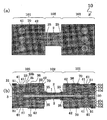
<第1の実施形態>
以下、本発明の実施形態について、図面を参照して説明する。図1(a)に、本発明の第1の実施形態の、リジッド部101とフレキ部102を併せ持つ10層のリジッドフレキシブルプリント配線板10の平面図を示し、図1(b)に、その側面の断面図を示す。図2〜図9は、第1の実施形態のリジッドフレキシブルプリント配線板10の製造方法を説明する側断面図及び平面図である。
<First Embodiment>
Hereinafter, embodiments of the present invention will be described with reference to the drawings. FIG. 1A shows a plan view of a 10-layer rigid flexible printed
図1(b)に示すように、第1の実施形態のリジッドフレキシブルプリント配線板10は、エポキシ樹脂、ポリイミド樹脂、ポリエステル樹脂などの有機樹脂からなる厚さが10μm以上で100μm以下で可撓性のあるフィルム状の支持フィルム1を中心に持つ。この支持フィルム1には図2(b)のように、貫通孔3aが形成され、その貫通孔3aに電解銅めっきの層を埋め込んだ金属めっき柱3を有し、支持フィルム1の表裏面には金属めっき柱3の半径よりの厚さが薄い銅めっき層を用いて配線パターン2が形成されている。
As shown in FIG.1 (b), the rigid flexible printed
図2(e)のように、配線パターン2が形成された可撓性のある絶縁樹脂から成る支持フィルム1の両面を、銅箔付きカバーレイフィルム20で覆う。銅箔付きカバーレイフィルム20は、片面に厚さ12μm程度の銅箔20aが張り合わされ、その銅箔20aの下層に厚さ8μm〜13μmのポリイミドフィルムなどの絶縁樹脂フィルム21を有する。
その絶縁樹脂フィルム21の層に接着剤層22が20μm程度の厚さに形成されている。銅箔付きカバーレイフィルム20は、全体の厚さが40μm〜50μmのフィルムである。この銅箔付きカバーレイフィルム20を支持フィルム1の両面に接着して内層フレキシブル配線板30を形成する。
As shown in FIG. 2 (e), both surfaces of the
An
そして、この内層フレキシブル配線板30の一部にリジッド部101を形成し、リジッド部101以外の内層フレキシブル配線板30の部分をフレキ部102としたリジッドフレキシブルプリント配線板10を製造する。
Then, the rigid flexible printed
このリジッドフレキシブルプリント配線板10は、特に、銅箔付きカバーレイフィルム20に形成したブラインドバイアホール23が、柱状に金属めっきを充填して形成され、それがその上層のビルドアップ層40dに柱状に金属めっきを充填して形成するブラインドバイアホール41と連結するとともに、下層の支持フィルム1中の金属めっき柱3と連結する強固な多層めっき柱が形成されている。
In this rigid flexible printed
その多層めっき柱はリジッド部101に食い込んで強固に保持されるとともに、ブラインドバイアホール23の上下に形成されたランド23bと4bが、カバーレイフィルム20の絶縁樹脂フィルム21と接着剤層22を、上下から保持する。それにより、カバーレイフィルム20が支持フィルム1及びリジッド部101の樹脂層に強固に結合され、カバーレイフィルム20と上下の樹脂層との接合の信頼性を向上させる効果がある。
The multi-layer plating pillars bite into the
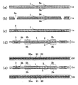
(製造方法)
以下で、図2から図9を参照して、本発明の実施形態の、10層のリジッドフレキシブルプリント配線板10の製造方法を説明する。
(Production method)
Below, with reference to FIGS. 2-9, the manufacturing method of the 10-layer rigid flexible printed
(内層フレキシブル配線板の製造方法)
先ず、リジッドフレキシブルプリント配線板10を構成する内層フレキシブル配線板30の製造方法を説明する。
(Inner layer flexible wiring board manufacturing method)
First, the manufacturing method of the inner layer
(工程1)
図2(a)のように、フレキ部102を形成する素材として、通常のフレキシブル配線板1aを準備する。そのフレキシブル配線板1aは、両面に銅箔2aを有し、銅箔2aを保持する支持フィルム1の基材がポリイミドなどの可撓性のある耐熱性樹脂から構成されるフレキシブル配線板1aである。ここで用いるフレキシブル配線板1aは、それを構成する銅箔2aと支持フィルム1の間には、屈曲性・折り曲げ性を高めるために、接着剤層は存在しない方が好ましいが、その間に接着剤層が存在するフレキシブル配線板1aを用いることも可能である。
(Process 1)
As shown in FIG. 2A, a normal flexible wiring board 1a is prepared as a material for forming the
(工程2)
次に、図2(b)のように、炭酸ガスレーザーやYAGレーザなどのレーザー穴あけ装置を用いて、穴あけ用レーザー光を照射することで貫通孔3aを穿孔する。形成する貫通孔3aの形状は、フレキシブル配線板1aの穴あけ用レーザー光を入射する側の表面に直径が80μmの開口をあけ、穴あけ用レーザー光がフレキシブル配線板1aを貫通して出射する側の表面の開口がそれより約30μm程度小さい直径50μmの円錐台状の貫通孔3aを形成する。
(Process 2)
Next, as shown in FIG. 2B, the through
(工程3)
次に、フレキシブル配線板1aの全面に触媒核を付与し、更に、無電解銅めっき浴に浸漬することで、厚さ0.1μmから数μmの無電解銅めっき皮膜を形成する。次に、図2(c)のように、平滑剤を添加した電解銅めっき液を用い、めっき浴をよく攪拌して、フ
レキシブル配線板1aの両面における銅めっき浴の流動速度を速くして電解銅めっきする。それにより、平滑剤は、フレキシブル配線板1aの両面への銅めっき層の成長を抑制する一方、貫通孔3aを埋める電解銅めっきの層の成長が抑制されない。そのため、貫通孔3aを電解銅めっきで充填した金属めっき柱3が形成される一方、フレキシブル配線板1aの第1の両面に形成される銅めっき層の厚さを、貫通孔3aの半径よりも薄く形成することができる。以上の処理により、貫通孔3aを埋め込む金属めっき柱3を形成し、フレキシブル配線板1aの両面に貫通孔3aの半径の4割の厚さの約16μmの厚さの銅めっき層を形成する。
(Process 3)
Next, a catalyst nucleus is imparted to the entire surface of the flexible wiring board 1a, and further immersed in an electroless copper plating bath to form an electroless copper plating film having a thickness of 0.1 μm to several μm. Next, as shown in FIG. 2 (c), using an electrolytic copper plating solution to which a smoothing agent is added, the plating bath is well stirred, and the flow rate of the copper plating bath on both sides of the flexible wiring board 1a is increased to perform electrolysis. Copper plating. Thereby, while the smoothing agent suppresses the growth of the copper plating layer on both surfaces of the flexible wiring board 1a, the growth of the electrolytic copper plating layer filling the through
(工程4)
次に、図2(d)のように、フレキシブル配線板1aの銅箔2aをエッチングすることで、金属めっき柱3の表側のランド3bと、ブラインドバイアホール24の下層の位置のランド2bと配線パターン2を形成する。
(Process 4)
Next, as shown in FIG. 2D, by etching the
(工程5)
図2(e)のような、銅箔20aとポリイミドフィルムなどの絶縁樹脂フィルム21と熱硬化性の接着剤層22とから成る銅箔付きカバーレイフィルム20を、フレキシブル配線板1aの両面に積層し、図3(f)のような基板を製造する。
(Process 5)
As shown in FIG. 2E, a
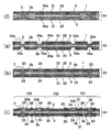
(工程6)
次に、図3(g)のように、その基板の、内層の金属めっき柱3の表側にあたる部分とランド2bの表側にあたる部分の銅箔付きカバーレイフィルム20の銅箔20aをエッチングして除去して、下地の絶縁樹脂フィルム21を露出させる。
(Step 6)
Next, as shown in FIG. 3 (g), the
(工程7)
そして、その露出した絶縁樹脂フィルム21の面に、炭酸ガスレーザー穴あけ装置のレーザー光を照射して、金属めっき柱3のランド3bに達するカバーレイ保持バイアホール用穴23aと、ランド2bに達するブラインドバイアホール用の穴24aを形成する。そのカバーレイ保持バイアホール用穴23a及びブラインドバイアホール用の穴24aの直径は、50〜150μm程度に形成する。
(Step 7)
Then, the exposed surface of the insulating
(工程8)
次に、その基板をデスミア液に浸漬することで、カバーレイ保持バイアホール用穴23a及びブラインドバイアホール用の穴24aのデスミア処理を行った上で、無電解銅めっき液に基板を浸漬することで、そのカバーレイ保持バイアホール用穴23a及びブラインドバイアホール用の穴24aの壁面に無電解銅めっき皮膜を形成する。
(Process 8)
Next, the substrate is immersed in an electroless copper plating solution after being subjected to desmear treatment of the cover-lay holding via
(工程9)
次に、図3(h)のように、その基板の下地の銅箔20aに電解銅めっき装置の陰極を接続して、基板を電解銅めっき浴に浸漬し基板の全面に電解銅めっきするパネルめっき処理を行う。それにより、基板のカバーレイ保持バイアホール用穴23aを銅めっきで柱状に充填してブラインドバイアホール23を形成し、ブラインドバイアホール用の穴24aを銅めっきで充填してブラインドバイアホール24を形成する。
(Step 9)
Next, as shown in FIG. 3 (h), the cathode of the electrolytic copper plating apparatus is connected to the
(工程10)
次に、図3(i)のように、エッチングレジストパターンで基板の表面の銅めっき層を保護してエッチングし、エッチング後にエッチングレジストを剥離する。
(Process 10)
Next, as shown in FIG. 3I, etching is performed while protecting the copper plating layer on the surface of the substrate with an etching resist pattern, and the etching resist is peeled off after the etching.
その銅めっき層のエッチングにより、絶縁樹脂フィルム21中に柱状のブラインドバイアホール23と24を有し、絶縁樹脂フィルム21の表面に、リジッド部101にブライ
ンドバイアホール23に接続するランド23bとブラインドバイアホール24に接続するランド24bと、位置合せマーク26のパターンと、補強用金属パターン25と、その他の配線パターンを形成する。
Etching of the copper plating layer has columnar blind via
特に、補強用金属パターン25は、リジッド部101とフレキ部102の境界部分に形成する。この補強用金属パターン25は、後にフレキ部102とリジッド部101の境界部分に照射する加工用レーザー光Lをその位置で遮断するストッパ層として用いる。
In particular, the reinforcing
工程10では、多層配線したフレキシブル配線板1a上に積層した薄いカバーレイフィルム20の層に埋め込んで形成したブラインドバイアホール23と24をビルドアップ層から多層配線したフレキシブル配線板1aの配線パターンに達するブラインドバイアホールとして形成し、そのブラインドバイアホールの高さを低くしたので、そのブラインドバイアホール23と24を、そのランド23bと24bの径を小さくして微細に形成できる。そのため、カバーレイの絶縁樹脂フィルム21上に配線パターンを高密度に形成できる効果がある。
In
また、カバーレイの絶縁樹脂フィルム21を、銅めっきの柱状のブラインドバイアホール23に接続するランド23bが上から支え、ブラインドバイアホール23の下に接続するランド3bが下から支える。すなわち、カバーレイの絶縁樹脂フィルム21を、柱状のブラインドバイアホール23に接続するランド23bとランド3bで上下から強固に支える。更に、ブラインドバイアホール23が、内層の金属めっき柱3に連結して支えられる。これにより、カバーレイの絶縁樹脂フィルム21が強固に保持される効果がある。
Further, the
特に、カバーレイの絶縁樹脂フィルム21に接する層の銅箔20aからランド23b及び24bを形成したので、ランド23b及び24bの層とその下のランド3b及び2bの層との間隔を小さくすることができる。それにより、それらの層のランドの間に挟み込む絶縁樹脂フィルム21と接着剤層22とを両層のランドで強く保持することができる効果がある。
In particular, since the
(工程11)
次に、図4(j)のように、カバーレイの絶縁樹脂フィルム21とその上の補強用金属パターン25上に薄剥離フィルム31を設置した内層フレキシブル配線板30を製造する。薄剥離フィルム31は、リジッドフレキシブルプリント配線板10のフレキ部102の領域を覆い補強用金属パターン25にかかる領域に設置する。薄剥離フィルム31の端部の位置は、位置合わせマーク26を基準にして、補強用金属パターン25上に後に形成する第1の溝27aと第2の溝27bの位置に、正確に位置を合わせて設置する。
(Step 11)
Next, as shown in FIG. 4 (j), an inner-layer
薄剥離フィルム31で覆われたフレキ部102は、リジッドフレキシブルプリント配線板10が完成した際に露出させる。薄剥離フィルム31には、フレキ部101の表面のカバーレイフィルム20から剥離がし易いフッ素系樹脂フィルム、PBTフィルム、PP延伸フィルム、PETフィルム、ポリオレフィンフィルム等を用いる。
The
(工程12)
次に、図4(k)のように、内層フレキシブル配線板30の両面に、回路パターン間への埋め込み性、及び積層後の表面平滑性に優れた溶融粘度が1000pois(10000Pa・s)以下のプリプレグ40aと薄銅箔40bを組み合わせ、加熱加圧成型することにより、図4(l)のようにビルドアップ層40dを形成する。
(Step 12)
Next, as shown in FIG. 4 (k), on both surfaces of the inner layer
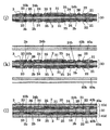
(工程13)
次に、図5(m)のように、炭酸ガスレーザー加工装置を使用して、位置合せマーク2
6を基準にしてレーザー光の照射位置を合わせたレーザー穴あけにより、薄銅箔40bの上から内層バイアホール41及び42用の穴41a及び42aを形成する。穴41a及び42aは、70〜150μm程度の直径を持ち、ブラインドバイアホール23及び24に達する穴を形成する。
(Step 13)
Next, as shown in FIG. 5 (m), using the carbon dioxide laser processing apparatus, the
The
(工程14)
次に、図5(n)のように、基板の全面に銅めっきするパネルめっき処理を行うことで、基板の内層バイアホール41及び42用の穴41a及び42aに銅めっきを充填し内層バイアホール41及び42を形成する。
(Step 14)
Next, as shown in FIG. 5 (n), by performing a panel plating process for copper plating on the entire surface of the substrate, the
(工程15)
次に、図5(o)のように、基板の表面の銅めっき層をエッチングすることで、ブラインドバイアホール23と24に連結するブラインドンバイアホール41と42のパターンと、加工用レーザーストッパ用銅箔パターン43を含む配線パターンを形成する。
(Step 15)
Next, as shown in FIG. 5 (o), by etching the copper plating layer on the surface of the substrate, the pattern of blind via
内層フレキシブル配線板30よりも下層に形成する加工用レーザーストッパ用銅箔パターン43は、後に、図8(t)のように、リジッドフレキシブルプリント配線板10の上面側から照射した加工用レーザー光Lを、内層フレキシブル配線板30よりも下面側の位置で遮断する位置に加工用レーザーストッパ用銅箔パターン43のパターンを形成する。
The processing laser stopper
ここで形成した加工用レーザーストッパ用銅箔パターン43は以下の様に用いる。すなわち、後の工程で、フレキ部102とリジッド部101の間の補強用金属パターン25の上に加工用レーザー光を照射してフレキ部102の表層のビルドアップ層とリジッド部101を切り離す溝を形成する。その際に、その加工用レーザー光を、加工用レーザーストッパ用銅箔パターン43で停止させて、それより下層で補強用金属パターン25までの間のビルドアップ層の樹脂には、加工用レーザーストッパ用銅箔パターン43以外の領域に加工用レーザー光を正確に位置を合わせて照射できる効果がある。
The
銅めっきの柱状のブラインドバイアホール24も、ブラインドバイアホール23と同様に、カバーレイの絶縁樹脂フィルム21を、ブラインドバイアホール24の上に接続するランド24bが上から支え、ブラインドバイアホール24の下に接続するランド2bが下から支える。すなわち、カバーレイの絶縁樹脂フィルム21を、柱状のブラインドバイアホール24に接続するランド24bとランド2bで上下から強固に支える。
Similarly to the blind via
更に、ブラインドバイアホール24が表側のビルドアップ層40dのブラインドバイアホール42に連結して支えられる。そして、ブラインドバイアホール42と24から成る柱状の銅めっきが、ビルドアップ層40dに埋め込まれて支えられる。
Further, the blind via
これにより、カバーレイの絶縁樹脂フィルム21がブラインドバイアホール24によっても強固に保持される効果がある。特に、カバーレイの絶縁樹脂フィルム21の上の銅箔20aを利用したランド24bと、カバーレイの下のランド2bでカバーレーを挟み込むため、そのランド24bとランド2bの間隔が狭いので、カバーレイが強く保持される効果がある。
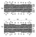
Accordingly, there is an effect that the insulating
(工程16)
次に、工程12から工程15まの処理と同様な処理を繰り返すことで、図6(p)のように、基板の両面の内層側から外層側に、ビルドアップ層50dと60dを順次に形成する。そのビルドアップ層50dには、ブラインドバイアホール41に連結するブラインドバイアホール51を形成し、ビルドアップ層60dには、そのブラインドバイアホール51に連結するブラインドバイアホール61を形成する。
(工程17)
次に、図6(q)のように、リジッド部101にソルダーレジスト70を印刷する。
(Step 16)
Next, by repeating the same process as the process from the process 12 to the process 15, the build-up
(Step 17)
Next, the solder resist 70 is printed on the
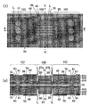
(工程18)
次に、図7(r)の平面図と図7(s)の側面図と図8(t)の側面図のように、位置合せマーク26を基準にして位置を合わせた炭酸ガスレーザーなどの加工用レーザー光Lを、フレキ部102とリジッド部101の境界部分の補強用金属パターン25の上の表層のビルドアップ層から補強用金属パターン25に達するまで照射する。すなわち、加工用レーザー光Lにより、フレキ部102の表層のビルドアップ層と図7(s)の左側のリジッド部101を切り離す第1の溝27aと、図7(s)の右側のリジッド部101を切り離す第2の溝27bを形成する。
(Step 18)
Next, as shown in the plan view of FIG. 7 (r), the side view of FIG. 7 (s), and the side view of FIG. 8 (t), a carbon dioxide laser or the like aligned with the
この加工は、カバーレイフィルム20の外層側の面に、位置合せマーク26が形成され、その位置合せマーク26を基準にして、補強用金属パターン25にかからせて設置した薄剥離フィルム31の端部に加工用レーザー光Lを正確に位置を合わせて照射することで第1の溝27aと第2の溝27bを形成する。それにより、薄剥離フィルム31が第1の溝27aと第2の溝27bの間のみに残留し、その薄剥離フィルム31がフレキ部の領域上のビルドアップ層にのみ残留するようにできる。そのため、フレキ部102の領域上のビルドアップ層を除去する際に薄剥離フィルム31も完全に除去して、リジッドフレキシブルプリント配線板10に残留させないようにできる効果がある。
In this processing, an
また、加工用レーザー光Lを基板の上面側と下面側から照射して、基板から、個々のリジッドフレキシブルプリント配線板10を切り出す。例えば、図8(t)のように、基板の上面側から照射した加工用レーザー光Lにより、内層フレキシブル配線板30よりも下面側の位置の加工用レーザーストッパ用銅箔パターン43に達するまで溝を形成し、基板から、リジッドフレキシブルプリント配線板10のフレキ部102を切り出す。
Further, the processing laser beam L is irradiated from the upper surface side and the lower surface side of the substrate, and the individual rigid flexible printed
(変形例1)
変形例1として、基板から、個々のリジッドフレキシブルプリント配線板10を切り出す外形加工については、機械的な外形ルーター加工で行うこともできる。
(Modification 1)
As a first modification, the outer shape processing for cutting out each rigid flexible printed
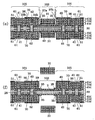
(工程19)
加工用レーザー光Lで基板に溝を形成した基板から、リジッドフレキシブルプリント配線板10のフレキ部102を切り出した後に、図8(u)及び図9(w)のように、基板の上面から、薄剥離フィルム31、及び、その上の、第1の溝27aと第2の溝27bの間の、ビルドアップ層40d、50d、60dとを引き剥がす。また、リジッドフレキシブルプリント配線板10から、下面の樹脂層を引き剥がす。すなわち、リジッドフレキシブルプリント配線板10の下面の、薄剥離フィルム31、及び、その下の、第1の溝27aと第2の溝27bの間の、基板の外枠部分と連結するビルドアップ層40d、50d、60dを引き剥がす。これにより、リジッドフレキシブルプリント配線板10のフレキ部102を、ビルドアップ層40d、及び50d、60dから引き剥がして、基板の外枠部分から個別のリジッドフレキシブルプリント配線板10を分離することができる。
(Step 19)
After cutting the
ここで、薄剥離フィルム31は、リジッドフレキシブルプリント配線板10のフレキ部102から剥離されて除去され、薄剥離フィルム31が残留しないので、フレキ部の表面の電気特性が薄剥離フィルム31の材質に影響されない効果がある。
Here, the
また、加工用レーザー光Lで形成した溝に露出したビルドアップ層40d、50d、60dの断面がリジッド部101の端部を成す。本実施形態で製造したリジッドフレキシブルプリント配線板10は、そのリジッド部101の端部の位置を、位置合せマーク26の
位置と比較する検査を行うことで、リジッド部101の端部の位置のズレ量を完成品で検査できる効果がある。
Further, the cross sections of the build-up
第1の実施形態では、内層フレキシブル配線板30内に形成したブラインドバイアホール23及び24がバイアホール41及び42と連結し、そのバイアホール41及び42がリジッド部101に食い込んで強固に保持される。それとともに、バイアホール23に狭い間隔を隔てて連結したランド23bと4b、及び、バイアホール24に狭い間隔を隔てて連結したランド24bと2bが、カバーレイフィルム20の絶縁樹脂フィルム21と接着剤層22を、上下から保持する。その構造がカバーレイフィルム20を、支持フィルム1及びリジッド部101のビルドアップ層40dに強固に結合させるので、カバーレイフィルム20と上下の樹脂層との接合の信頼性を高くできる効果がある。
In the first embodiment, the blind via
特に、第1の実施形態では、補強用金属パターン25が平坦なカバーレイフィルム20を表層側から押さえて補強する効果がある。また、リジッド部101とフレキ部102の境界部分は、補強用金属パターン25の上面に達する加工用レーザー光Lで形成した溝27a、27bで分離されていて、しかも、フレキ部102の表面を覆う薄剥離フィルム31がビルドアップ層とともにフレキ部102から除去されるので、補強用金属パターン25の上面に樹脂が被さらない。リジッド部101側では、ビルドアップ層の端部が、加工用レーザー光Lで形成した溝27a、27bの側面として補強用金属パターン25上に垂直に形成されて、補強用金属パターン25の上面に樹脂が被さらないため、リジッド部101とフレキ部102の境界部分に柔軟性があり、屈曲の繰り返しへの耐久力が高い効果がある。
In particular, in the first embodiment, the reinforcing
<第2の実施形態>
図10〜図11は、本発明の第2の実施形態のリジッドフレキシブルプリント配線板10の製造方法を説明する側断面図である。図11(f)に、第2の実施形態の、リジッドフレキシブルプリント配線板10の側断面図を示す。
<Second Embodiment>
FIGS. 10-11 is a sectional side view explaining the manufacturing method of the rigid flexible printed
(製造方法)
(工程1:内層フレキシブル配線板の製造)
図11(f)に示すように、第2の実施形態のリジッドフレキシブルプリント配線板10は、可撓性のあるフィルム状の支持フィルム1を中心に持つ。図10(a)のように、この支持フィルム1の表裏面には配線パターン2とランド2bとランド3bを形成する。
(Production method)
(Process 1: Production of inner layer flexible wiring board)
As shown in FIG. 11 (f), the rigid flexible printed
(工程2)
次に、図10(b)のように、その支持フィルム1の両面に、銅箔20aと絶縁樹脂フィルム21と接着剤層22とから成る銅箔付きカバーレイフィルム20を積層することで内層フレキシブル配線板30を形成する。
(Process 2)
Next, as shown in FIG. 10 (b), the inner layer flexible is obtained by laminating a
(工程3)
次に、図10(c)のように、ドリルで、ランド2bと4bの位置に、上下の銅箔付きカバーレイフィルム20とその間の支持フィルム1を貫通する貫通孔を形成する。
(Process 3)
Next, as shown in FIG. 10C, through holes are formed by drills at the positions of the
(工程4)
そして、その貫通孔の壁面に銅めっきすることでスルーホール28と29を形成する。次に、そのスルーホール28と29の孔内に孔埋め剤を充填し、その孔埋め剤が充填されたスルーホール28と29の上下の表面に銅めっき層を形成する。
(Process 4)
Then, the through
(工程5)
次に、その銅めっき層をエッチングして、リジッド部101に、スルーホール28と接
続するランド23bのパターンと、スルーホール29と接続するランド24bのパターンと、位置合せマーク26のパターンを形成し、リジッド部101とフレキ部102の境界部分に補強用金属パターン25を形成する。
(Process 5)
Next, the copper plating layer is etched to form a pattern of
カバーレイの絶縁樹脂フィルム21を、スルーホール28に接続するランド23bが上から支え、下に接続するランド3bが下から支える。すなわち、カバーレイの絶縁樹脂フィルム21を、スルーホール28に接続するランド23bとランド3bで上下から強固に支える。同じく、スルーホール29に接続するランド24bとランド2bでカバーレイの絶縁樹脂フィルム21を上下から強固に支える。これにより、カバーレイの絶縁樹脂フィルム21が強固に保持される効果がある。
A
ここで、第1の実施形態と同様に、カバーレイの絶縁樹脂フィルム21に接する層の銅箔20aから銅箔20aからランド23b及び24bを形成したので、ランド23b及び24bとその下のランド3b及び2bとの間隔を小さくすることで、その間に挟み込むカバーレイの絶縁樹脂フィルム21と接着剤層22とを強く保持することができる効果がある。
Here, as in the first embodiment, since the
(工程6)
次に、図10(d)のように、リジッドフレキシブルプリント配線板10のフレキ部102の領域を覆い補強用金属パターン25にかかる領域に薄剥離フィルム31を設置して内層フレキシブル配線板30を製造する。ここで、薄剥離フィルム31は、位置合わせマーク26で位置を合わせることで、その端部の位置を補強用金属パターン25上の第1の溝27aと第2の溝27bの位置に正確に位置を合わせて設置する。
(Step 6)
Next, as shown in FIG. 10 (d), an inner layer
(工程7)
次に、第1の実施形態の工程12から工程17まの処理を行うことで、図11(e)のように、基板の両面の内層側から外層側に、ビルドアップ層40dと50dと60dを順次に形成する。そのビルドアップ層40dには、スルーホール28のランド23bと連結するブラインドバイアホール41と、スルーホール29のランド24bと連結するブラインドバイアホール42を形成し、ビルドアップ層50dには、ブラインドバイアホール41に連結するブラインドバイアホール51を形成し、ビルドアップ層60dには、そのブラインドバイアホール51に連結するブラインドバイアホール61を形成する。次に、リジッド部101にソルダーレジスト70を印刷する。
(Step 7)
Next, by performing the processing from step 12 to step 17 of the first embodiment, as shown in FIG. 11E, the buildup layers 40d, 50d, and 60d are formed from the inner layer side to the outer layer side of both surfaces of the substrate. Are formed sequentially. A blind via
(工程8)
次に、第1の実施形態の工程18と同様にして、炭酸ガスレーザーなどの加工用レーザー光Lを基板の上面側と下面側から照射して、基板から、個々のリジッドフレキシブルプリント配線板10を切り出す。
(Process 8)
Next, in the same manner as in step 18 of the first embodiment, a processing laser beam L such as a carbon dioxide laser is irradiated from the upper surface side and the lower surface side of the substrate, and each rigid flexible printed
(工程9)
次に、図11(f)のように、第1の実施形態の工程19と同様にして、基板の薄剥離フィルム31からリジッドフレキシブルプリント配線板10のフレキ部102を引き剥がして分離することで基板の外枠部分から個別のリジッドフレキシブルプリント配線板10を分離する。
(Step 9)
Next, as shown in FIG. 11 (f), the
第2の実施形態のリジッドフレキシブルプリント配線板10は、特に、スルーホール28及び27を形成したことが第1の実施形態と異なる。第2の実施形態では、内層フレキシブル配線板30内に形成したスルーホール28及び29がバイアホール41及び42と連結し、そのバイアホール41及び42がリジッド部101に食い込んで強固に保持される。それとともに、スルーホール28に狭い間隔を隔てて連結したランド23bと4b、及び、スルーホール29に狭い間隔を隔てて連結したランド24bと2bが、カバーレイフィルム20の絶縁樹脂フィルム21と接着剤層22を、上下から保持する。その構造がカバーレイフィルム20を、支持フィルム1及びリジッド部101のビルドアップ層40dに強固に結合させるので、カバーレイフィルム20と上下の樹脂層との接合の信頼性を高くできる効果がある。
The rigid flexible printed
なお、本発明は、上記の実施形態に限定されず、カバーレイの絶縁樹脂フィルム21上に形成する位置合せマーク26の位置は、リジッド部101に限定されず、フレキ部102に位置合せマーク26を形成することもできる。フレキ部102に位置合せマーク26を形成すると、位置合せマーク26がフレキ部102に露出して、その位置の観察が容易になるので、位置合せマーク26に位置を合わせて形成されたリジッドフレキシブルプリント配線板10各部との位置ずれの測定が容易になる効果がある。例えば、補強用金属パターン25上に溝27aと27bによって垂直に形成されたビルドアップ層40d、50d、60dの端部の側面の位置と位置合せマーク26との相対位置のずれ量の測定が容易になる効果がある。
In addition, this invention is not limited to said embodiment, The position of the
1・・・支持フィルム
1a・・・フレキシブル配線板
2・・・配線パターン
2a・・・銅箔
2b・・・ランド
3・・・金属めっき柱
3a・・・貫通孔
3b・・・ランド
10・・・リジッドフレキシブルプリント配線板
20・・・銅箔付きカバーレイフィルム
20a・・・銅箔
21・・・絶縁樹脂フィルム
22・・・接着剤層
23、24、41、42、51、61・・・・ブラインドバイアホール
23a・・・カバーレイ保持バイアホール用穴
23b・・・カバーレイ保持バイアホール用ランド
24a・・・ブラインドバイアホール用の穴
24b・・・ブラインドバイアホール用ランド
25・・・補強用金属パターン
26・・・位置合せマーク
27a・・・第1の溝
27b・・・第2の溝
28、29・・・スルーホール
30・・・内層フレキシブル配線板
31・・・薄剥離フィルム
40a・・・プリプレグ
40b・・・薄銅箔
40d、50d、60d・・・ビルドアップ層
43・・・加工用レーザーストッパ用銅箔パターン
101・・・リジッド部
102・・・フレキ部
L・・・加工用レーザー光
DESCRIPTION OF
Claims (3)
Priority Applications (1)
| Application Number | Priority Date | Filing Date | Title |
|---|---|---|---|
| JP2011070023A JP2012204749A (en) | 2011-03-28 | 2011-03-28 | Rigid flexible printed wiring board and method of manufacturing the same |
Applications Claiming Priority (1)
| Application Number | Priority Date | Filing Date | Title |
|---|---|---|---|
| JP2011070023A JP2012204749A (en) | 2011-03-28 | 2011-03-28 | Rigid flexible printed wiring board and method of manufacturing the same |
Publications (1)
| Publication Number | Publication Date |
|---|---|
| JP2012204749A true JP2012204749A (en) | 2012-10-22 |
Family
ID=47185346
Family Applications (1)
| Application Number | Title | Priority Date | Filing Date |
|---|---|---|---|
| JP2011070023A Pending JP2012204749A (en) | 2011-03-28 | 2011-03-28 | Rigid flexible printed wiring board and method of manufacturing the same |
Country Status (1)
| Country | Link |
|---|---|
| JP (1) | JP2012204749A (en) |
Cited By (4)
| Publication number | Priority date | Publication date | Assignee | Title |
|---|---|---|---|---|
| WO2017070992A1 (en) * | 2015-10-28 | 2017-05-04 | 安捷利电子科技(苏州)有限公司 | Method for full filling inter-layer blind hole of hdi rigid-flex laminate with copper |
| JP2017152493A (en) * | 2016-02-23 | 2017-08-31 | 京セラ株式会社 | Method for manufacturing printed wiring board |
| JP2019029635A (en) * | 2017-07-26 | 2019-02-21 | サムソン エレクトロ−メカニックス カンパニーリミテッド. | Rigid flexible printed circuit board and manufacturing method thereof |
| CN113179597A (en) * | 2021-04-22 | 2021-07-27 | 深圳市格瑞弘电子有限公司 | Rigid-flexible circuit board and manufacturing method thereof |
Citations (6)
| Publication number | Priority date | Publication date | Assignee | Title |
|---|---|---|---|---|
| JPH03141693A (en) * | 1989-10-26 | 1991-06-17 | Aica Kogyo Co Ltd | Rigid flexible composite multilayer printed circuit board and manufacture thereof |
| JP2001251053A (en) * | 2000-03-06 | 2001-09-14 | Sony Corp | Printed wiring board and method for manufacturing printed wiring board |
| JP2005268568A (en) * | 2004-03-19 | 2005-09-29 | Cmk Corp | Production method of multilayer printed wiring board |
| JP2006287007A (en) * | 2005-04-01 | 2006-10-19 | Cmk Corp | Multilayer printed circuit board and its manufacturing method |
| JP2007324208A (en) * | 2006-05-30 | 2007-12-13 | Toshiba Corp | Printed wiring board, method of manufacturing the same and electronic device |
| JP2008034433A (en) * | 2006-07-26 | 2008-02-14 | Cmk Corp | Rigid flex printed-wiring board, and manufacturing method thereof |
-
2011
- 2011-03-28 JP JP2011070023A patent/JP2012204749A/en active Pending
Patent Citations (6)
| Publication number | Priority date | Publication date | Assignee | Title |
|---|---|---|---|---|
| JPH03141693A (en) * | 1989-10-26 | 1991-06-17 | Aica Kogyo Co Ltd | Rigid flexible composite multilayer printed circuit board and manufacture thereof |
| JP2001251053A (en) * | 2000-03-06 | 2001-09-14 | Sony Corp | Printed wiring board and method for manufacturing printed wiring board |
| JP2005268568A (en) * | 2004-03-19 | 2005-09-29 | Cmk Corp | Production method of multilayer printed wiring board |
| JP2006287007A (en) * | 2005-04-01 | 2006-10-19 | Cmk Corp | Multilayer printed circuit board and its manufacturing method |
| JP2007324208A (en) * | 2006-05-30 | 2007-12-13 | Toshiba Corp | Printed wiring board, method of manufacturing the same and electronic device |
| JP2008034433A (en) * | 2006-07-26 | 2008-02-14 | Cmk Corp | Rigid flex printed-wiring board, and manufacturing method thereof |
Cited By (5)
| Publication number | Priority date | Publication date | Assignee | Title |
|---|---|---|---|---|
| WO2017070992A1 (en) * | 2015-10-28 | 2017-05-04 | 安捷利电子科技(苏州)有限公司 | Method for full filling inter-layer blind hole of hdi rigid-flex laminate with copper |
| JP2017152493A (en) * | 2016-02-23 | 2017-08-31 | 京セラ株式会社 | Method for manufacturing printed wiring board |
| JP2019029635A (en) * | 2017-07-26 | 2019-02-21 | サムソン エレクトロ−メカニックス カンパニーリミテッド. | Rigid flexible printed circuit board and manufacturing method thereof |
| JP7102665B2 (en) | 2017-07-26 | 2022-07-20 | サムソン エレクトロ-メカニックス カンパニーリミテッド. | Rigid flexible printed circuit board and its manufacturing method {RIGID FLEXIBLE PRINTED CIRCUIT BOARD AND THE MANUFACTURING METHOD THEREOF} |
| CN113179597A (en) * | 2021-04-22 | 2021-07-27 | 深圳市格瑞弘电子有限公司 | Rigid-flexible circuit board and manufacturing method thereof |
Similar Documents
| Publication | Publication Date | Title |
|---|---|---|
| TWI593064B (en) | Method of manufacturing substrate with built-in element and substrate with built-in element manufactured by the method | |
| JP6208449B2 (en) | Manufacturing method of multilayer wiring board | |
| JP5688162B2 (en) | Method for manufacturing component-embedded substrate and component-embedded substrate manufactured using this method | |
| JP2013175495A (en) | Component built-in printed circuit board and method of manufacturing the same | |
| WO2014104328A1 (en) | Layered body with support substrate, method for fabricating same, and method for fabricating multi-layer wiring substrate | |
| TW201424501A (en) | Package structure and method for manufacturing same | |
| JP2012216575A (en) | Component built-in printed circuit board and manufacturing method thereof | |
| KR20090038635A (en) | Manufacturing method of multi-layer circuit board | |
| JP2012204749A (en) | Rigid flexible printed wiring board and method of manufacturing the same | |
| JP5485299B2 (en) | Manufacturing method of multilayer printed wiring board | |
| JP2013168691A (en) | Printed circuit board and method for filling via hole thereof | |
| JP2012234937A (en) | Rigid flexible printed circuit board and manufacturing method therefor | |
| JP6016004B2 (en) | Wiring board and manufacturing method thereof | |
| KR101170764B1 (en) | Method for manufacturing Multi-layer circuit board | |
| KR20040085374A (en) | Method for making through-hole of multi-layer flexible printed circuit board | |
| JP2013074270A (en) | Manufacturing method of rigid flexible printed wiring board | |
| JP2013051325A (en) | Rigid flexible printed wiring board manufacturing method | |
| JP2010010488A (en) | Manufacturing method of wiring board, and wiring board | |
| JP2005236194A (en) | Manufacturing method for printed-wiring board | |
| JP6076431B2 (en) | Manufacturing method of semiconductor package substrate | |
| JP2015144148A (en) | Laminate with support substrate, manufacturing method thereof, and manufacturing method of multilayer wiring board | |
| JP4633457B2 (en) | Manufacturing method of rigid flexible printed wiring board | |
| JP2010262954A (en) | Method for manufacturing wiring board | |
| JP2007311484A (en) | Printed-wiring board, and manufacturing method therefor | |
| JP2015159223A (en) | Post electrode, method of manufacturing post electrode and circuit board |
Legal Events
| Date | Code | Title | Description |
|---|---|---|---|
| A621 | Written request for application examination |
Free format text: JAPANESE INTERMEDIATE CODE: A621 Effective date: 20140328 |
|
| A711 | Notification of change in applicant |
Free format text: JAPANESE INTERMEDIATE CODE: A712 Effective date: 20141104 |
|
| A977 | Report on retrieval |
Free format text: JAPANESE INTERMEDIATE CODE: A971007 Effective date: 20141114 |
|
| A131 | Notification of reasons for refusal |
Free format text: JAPANESE INTERMEDIATE CODE: A131 Effective date: 20141218 |
|
| A02 | Decision of refusal |
Free format text: JAPANESE INTERMEDIATE CODE: A02 Effective date: 20150420 |