JP2012174607A - Organic el device - Google Patents
Organic el device Download PDFInfo
- Publication number
- JP2012174607A JP2012174607A JP2011037447A JP2011037447A JP2012174607A JP 2012174607 A JP2012174607 A JP 2012174607A JP 2011037447 A JP2011037447 A JP 2011037447A JP 2011037447 A JP2011037447 A JP 2011037447A JP 2012174607 A JP2012174607 A JP 2012174607A
- Authority
- JP
- Japan
- Prior art keywords
- layer
- substrate
- organic
- electrode
- anode
- Prior art date
- Legal status (The legal status is an assumption and is not a legal conclusion. Google has not performed a legal analysis and makes no representation as to the accuracy of the status listed.)
- Withdrawn
Links
- 239000010410 layer Substances 0.000 claims abstract description 150
- 239000000758 substrate Substances 0.000 claims abstract description 115
- 239000012044 organic layer Substances 0.000 claims abstract description 66
- 238000009499 grossing Methods 0.000 claims abstract description 16
- 238000000605 extraction Methods 0.000 claims description 57
- 239000012790 adhesive layer Substances 0.000 claims description 25
- 239000003566 sealing material Substances 0.000 claims description 16
- 230000004888 barrier function Effects 0.000 claims description 12
- 230000002093 peripheral effect Effects 0.000 claims description 11
- 238000010521 absorption reaction Methods 0.000 claims description 5
- 230000015572 biosynthetic process Effects 0.000 abstract description 5
- 238000004519 manufacturing process Methods 0.000 abstract description 5
- 230000003287 optical effect Effects 0.000 abstract 1
- 238000005401 electroluminescence Methods 0.000 description 42
- 239000000463 material Substances 0.000 description 36
- -1 etc. Polymers 0.000 description 25
- 238000000034 method Methods 0.000 description 18
- 229910052782 aluminium Inorganic materials 0.000 description 15
- XAGFODPZIPBFFR-UHFFFAOYSA-N aluminium Chemical compound [Al] XAGFODPZIPBFFR-UHFFFAOYSA-N 0.000 description 15
- 229910052751 metal Inorganic materials 0.000 description 13
- 239000002184 metal Substances 0.000 description 13
- 229920005989 resin Polymers 0.000 description 12
- 239000011347 resin Substances 0.000 description 12
- 150000001875 compounds Chemical class 0.000 description 9
- 238000007789 sealing Methods 0.000 description 8
- 239000000203 mixture Substances 0.000 description 6
- 229920000178 Acrylic resin Polymers 0.000 description 5
- 239000004925 Acrylic resin Substances 0.000 description 5
- BQCADISMDOOEFD-UHFFFAOYSA-N Silver Chemical compound [Ag] BQCADISMDOOEFD-UHFFFAOYSA-N 0.000 description 5
- 239000000470 constituent Substances 0.000 description 5
- 239000010408 film Substances 0.000 description 5
- 239000011521 glass Substances 0.000 description 5
- 239000011368 organic material Substances 0.000 description 5
- 229910052709 silver Inorganic materials 0.000 description 5
- 239000004332 silver Substances 0.000 description 5
- PXHVJJICTQNCMI-UHFFFAOYSA-N Nickel Chemical compound [Ni] PXHVJJICTQNCMI-UHFFFAOYSA-N 0.000 description 4
- 239000004698 Polyethylene Substances 0.000 description 4
- 239000004743 Polypropylene Substances 0.000 description 4
- 239000007983 Tris buffer Substances 0.000 description 4
- 229910045601 alloy Inorganic materials 0.000 description 4
- 239000000956 alloy Substances 0.000 description 4
- 239000004020 conductor Substances 0.000 description 4
- ZSWFCLXCOIISFI-UHFFFAOYSA-N cyclopentadiene Chemical compound C1C=CC=C1 ZSWFCLXCOIISFI-UHFFFAOYSA-N 0.000 description 4
- 230000005525 hole transport Effects 0.000 description 4
- 238000002347 injection Methods 0.000 description 4
- 239000007924 injection Substances 0.000 description 4
- 150000002739 metals Chemical class 0.000 description 4
- 238000000059 patterning Methods 0.000 description 4
- 229920000573 polyethylene Polymers 0.000 description 4
- 229920001155 polypropylene Polymers 0.000 description 4
- RYGMFSIKBFXOCR-UHFFFAOYSA-N Copper Chemical compound [Cu] RYGMFSIKBFXOCR-UHFFFAOYSA-N 0.000 description 3
- 239000004793 Polystyrene Substances 0.000 description 3
- 230000006866 deterioration Effects 0.000 description 3
- 238000007607 die coating method Methods 0.000 description 3
- 239000007772 electrode material Substances 0.000 description 3
- 239000003822 epoxy resin Substances 0.000 description 3
- PCHJSUWPFVWCPO-UHFFFAOYSA-N gold Chemical compound [Au] PCHJSUWPFVWCPO-UHFFFAOYSA-N 0.000 description 3
- 229910052737 gold Inorganic materials 0.000 description 3
- 239000010931 gold Substances 0.000 description 3
- 229920000647 polyepoxide Polymers 0.000 description 3
- 229920000139 polyethylene terephthalate Polymers 0.000 description 3
- 239000005020 polyethylene terephthalate Substances 0.000 description 3
- 229920001721 polyimide Polymers 0.000 description 3
- 229920000642 polymer Polymers 0.000 description 3
- 229920002223 polystyrene Polymers 0.000 description 3
- 239000011118 polyvinyl acetate Substances 0.000 description 3
- 229920002689 polyvinyl acetate Polymers 0.000 description 3
- 238000005096 rolling process Methods 0.000 description 3
- 238000007650 screen-printing Methods 0.000 description 3
- 239000000126 substance Substances 0.000 description 3
- 229920005992 thermoplastic resin Polymers 0.000 description 3
- 229920001187 thermosetting polymer Polymers 0.000 description 3
- VFUDMQLBKNMONU-UHFFFAOYSA-N 9-[4-(4-carbazol-9-ylphenyl)phenyl]carbazole Chemical group C12=CC=CC=C2C2=CC=CC=C2N1C1=CC=C(C=2C=CC(=CC=2)N2C3=CC=CC=C3C3=CC=CC=C32)C=C1 VFUDMQLBKNMONU-UHFFFAOYSA-N 0.000 description 2
- XEEYBQQBJWHFJM-UHFFFAOYSA-N Iron Chemical compound [Fe] XEEYBQQBJWHFJM-UHFFFAOYSA-N 0.000 description 2
- TWRXJAOTZQYOKJ-UHFFFAOYSA-L Magnesium chloride Chemical compound [Mg+2].[Cl-].[Cl-] TWRXJAOTZQYOKJ-UHFFFAOYSA-L 0.000 description 2
- CSNNHWWHGAXBCP-UHFFFAOYSA-L Magnesium sulfate Chemical compound [Mg+2].[O-][S+2]([O-])([O-])[O-] CSNNHWWHGAXBCP-UHFFFAOYSA-L 0.000 description 2
- UFWIBTONFRDIAS-UHFFFAOYSA-N Naphthalene Chemical compound C1=CC=CC2=CC=CC=C21 UFWIBTONFRDIAS-UHFFFAOYSA-N 0.000 description 2
- 239000004952 Polyamide Substances 0.000 description 2
- 229920001328 Polyvinylidene chloride Polymers 0.000 description 2
- ATJFFYVFTNAWJD-UHFFFAOYSA-N Tin Chemical compound [Sn] ATJFFYVFTNAWJD-UHFFFAOYSA-N 0.000 description 2
- RTAQQCXQSZGOHL-UHFFFAOYSA-N Titanium Chemical compound [Ti] RTAQQCXQSZGOHL-UHFFFAOYSA-N 0.000 description 2
- XLOMVQKBTHCTTD-UHFFFAOYSA-N Zinc monoxide Chemical compound [Zn]=O XLOMVQKBTHCTTD-UHFFFAOYSA-N 0.000 description 2
- 229910052783 alkali metal Inorganic materials 0.000 description 2
- 150000001340 alkali metals Chemical class 0.000 description 2
- 239000010405 anode material Substances 0.000 description 2
- MWPLVEDNUUSJAV-UHFFFAOYSA-N anthracene Chemical compound C1=CC=CC2=CC3=CC=CC=C3C=C21 MWPLVEDNUUSJAV-UHFFFAOYSA-N 0.000 description 2
- 150000004982 aromatic amines Chemical class 0.000 description 2
- QVQLCTNNEUAWMS-UHFFFAOYSA-N barium oxide Chemical compound [Ba]=O QVQLCTNNEUAWMS-UHFFFAOYSA-N 0.000 description 2
- 239000011230 binding agent Substances 0.000 description 2
- OSGAYBCDTDRGGQ-UHFFFAOYSA-L calcium sulfate Chemical compound [Ca+2].[O-]S([O-])(=O)=O OSGAYBCDTDRGGQ-UHFFFAOYSA-L 0.000 description 2
- 239000011248 coating agent Substances 0.000 description 2
- 238000000576 coating method Methods 0.000 description 2
- 229910052802 copper Inorganic materials 0.000 description 2
- 239000010949 copper Substances 0.000 description 2
- VPUGDVKSAQVFFS-UHFFFAOYSA-N coronene Chemical compound C1=C(C2=C34)C=CC3=CC=C(C=C3)C4=C4C3=CC=C(C=C3)C4=C2C3=C1 VPUGDVKSAQVFFS-UHFFFAOYSA-N 0.000 description 2
- ZYGHJZDHTFUPRJ-UHFFFAOYSA-N coumarin Chemical compound C1=CC=C2OC(=O)C=CC2=C1 ZYGHJZDHTFUPRJ-UHFFFAOYSA-N 0.000 description 2
- 239000002274 desiccant Substances 0.000 description 2
- 239000002019 doping agent Substances 0.000 description 2
- 238000001035 drying Methods 0.000 description 2
- 239000011888 foil Substances 0.000 description 2
- 238000007756 gravure coating Methods 0.000 description 2
- 239000011133 lead Substances 0.000 description 2
- IBHBKWKFFTZAHE-UHFFFAOYSA-N n-[4-[4-(n-naphthalen-1-ylanilino)phenyl]phenyl]-n-phenylnaphthalen-1-amine Chemical group C1=CC=CC=C1N(C=1C2=CC=CC=C2C=CC=1)C1=CC=C(C=2C=CC(=CC=2)N(C=2C=CC=CC=2)C=2C3=CC=CC=C3C=CC=2)C=C1 IBHBKWKFFTZAHE-UHFFFAOYSA-N 0.000 description 2
- 229910052759 nickel Inorganic materials 0.000 description 2
- WCPAKWJPBJAGKN-UHFFFAOYSA-N oxadiazole Chemical compound C1=CON=N1 WCPAKWJPBJAGKN-UHFFFAOYSA-N 0.000 description 2
- 229920003227 poly(N-vinyl carbazole) Polymers 0.000 description 2
- 229920003229 poly(methyl methacrylate) Polymers 0.000 description 2
- 229920002647 polyamide Polymers 0.000 description 2
- 239000009719 polyimide resin Substances 0.000 description 2
- 239000004926 polymethyl methacrylate Substances 0.000 description 2
- 229920002635 polyurethane Polymers 0.000 description 2
- 239000004814 polyurethane Substances 0.000 description 2
- 239000005033 polyvinylidene chloride Substances 0.000 description 2
- 238000002360 preparation method Methods 0.000 description 2
- BBEAQIROQSPTKN-UHFFFAOYSA-N pyrene Chemical compound C1=CC=C2C=CC3=CC=CC4=CC=C1C2=C43 BBEAQIROQSPTKN-UHFFFAOYSA-N 0.000 description 2
- 229920002050 silicone resin Polymers 0.000 description 2
- 238000004528 spin coating Methods 0.000 description 2
- 238000005507 spraying Methods 0.000 description 2
- 239000011135 tin Substances 0.000 description 2
- 229910052718 tin Inorganic materials 0.000 description 2
- 239000010936 titanium Substances 0.000 description 2
- 229910052719 titanium Inorganic materials 0.000 description 2
- UWRZIZXBOLBCON-VOTSOKGWSA-N (e)-2-phenylethenamine Chemical class N\C=C\C1=CC=CC=C1 UWRZIZXBOLBCON-VOTSOKGWSA-N 0.000 description 1
- NGQSLSMAEVWNPU-YTEMWHBBSA-N 1,2-bis[(e)-2-phenylethenyl]benzene Chemical class C=1C=CC=CC=1/C=C/C1=CC=CC=C1\C=C\C1=CC=CC=C1 NGQSLSMAEVWNPU-YTEMWHBBSA-N 0.000 description 1
- KLCLIOISYBHYDZ-UHFFFAOYSA-N 1,4,4-triphenylbuta-1,3-dienylbenzene Chemical compound C=1C=CC=CC=1C(C=1C=CC=CC=1)=CC=C(C=1C=CC=CC=1)C1=CC=CC=C1 KLCLIOISYBHYDZ-UHFFFAOYSA-N 0.000 description 1
- GUPMCMZMDAGSPF-UHFFFAOYSA-N 1-phenylbuta-1,3-dienylbenzene Chemical compound C=1C=CC=CC=1[C](C=C[CH2])C1=CC=CC=C1 GUPMCMZMDAGSPF-UHFFFAOYSA-N 0.000 description 1
- MQRCTQVBZYBPQE-UHFFFAOYSA-N 189363-47-1 Chemical compound C1=CC=CC=C1N(C=1C=C2C3(C4=CC(=CC=C4C2=CC=1)N(C=1C=CC=CC=1)C=1C=CC=CC=1)C1=CC(=CC=C1C1=CC=C(C=C13)N(C=1C=CC=CC=1)C=1C=CC=CC=1)N(C=1C=CC=CC=1)C=1C=CC=CC=1)C1=CC=CC=C1 MQRCTQVBZYBPQE-UHFFFAOYSA-N 0.000 description 1
- QZTQQBIGSZWRGI-UHFFFAOYSA-N 2-n',7-n'-bis(3-methylphenyl)-2-n',7-n'-diphenyl-9,9'-spirobi[fluorene]-2',7'-diamine Chemical compound CC1=CC=CC(N(C=2C=CC=CC=2)C=2C=C3C4(C5=CC=CC=C5C5=CC=CC=C54)C4=CC(=CC=C4C3=CC=2)N(C=2C=CC=CC=2)C=2C=C(C)C=CC=2)=C1 QZTQQBIGSZWRGI-UHFFFAOYSA-N 0.000 description 1
- HONWGFNQCPRRFM-UHFFFAOYSA-N 2-n-(3-methylphenyl)-1-n,1-n,2-n-triphenylbenzene-1,2-diamine Chemical compound CC1=CC=CC(N(C=2C=CC=CC=2)C=2C(=CC=CC=2)N(C=2C=CC=CC=2)C=2C=CC=CC=2)=C1 HONWGFNQCPRRFM-UHFFFAOYSA-N 0.000 description 1
- MGADZUXDNSDTHW-UHFFFAOYSA-N 2H-pyran Chemical compound C1OC=CC=C1 MGADZUXDNSDTHW-UHFFFAOYSA-N 0.000 description 1
- GOLORTLGFDVFDW-UHFFFAOYSA-N 3-(1h-benzimidazol-2-yl)-7-(diethylamino)chromen-2-one Chemical compound C1=CC=C2NC(C3=CC4=CC=C(C=C4OC3=O)N(CC)CC)=NC2=C1 GOLORTLGFDVFDW-UHFFFAOYSA-N 0.000 description 1
- ONKCIMOQGCARHN-UHFFFAOYSA-N 3-methyl-n-[4-[4-(3-methylanilino)phenyl]phenyl]aniline Chemical compound CC1=CC=CC(NC=2C=CC(=CC=2)C=2C=CC(NC=3C=C(C)C=CC=3)=CC=2)=C1 ONKCIMOQGCARHN-UHFFFAOYSA-N 0.000 description 1
- WEELZNKFYGCZKL-UHFFFAOYSA-N 4-(4-phenylphenyl)-n,n-bis[4-(4-phenylphenyl)phenyl]aniline Chemical compound C1=CC=CC=C1C1=CC=C(C=2C=CC(=CC=2)N(C=2C=CC(=CC=2)C=2C=CC(=CC=2)C=2C=CC=CC=2)C=2C=CC(=CC=2)C=2C=CC(=CC=2)C=2C=CC=CC=2)C=C1 WEELZNKFYGCZKL-UHFFFAOYSA-N 0.000 description 1
- 229910018072 Al 2 O 3 Inorganic materials 0.000 description 1
- 229910001148 Al-Li alloy Inorganic materials 0.000 description 1
- UXVMQQNJUSDDNG-UHFFFAOYSA-L Calcium chloride Chemical compound [Cl-].[Cl-].[Ca+2] UXVMQQNJUSDDNG-UHFFFAOYSA-L 0.000 description 1
- OKTJSMMVPCPJKN-UHFFFAOYSA-N Carbon Chemical compound [C] OKTJSMMVPCPJKN-UHFFFAOYSA-N 0.000 description 1
- 150000000918 Europium Chemical class 0.000 description 1
- DGAQECJNVWCQMB-PUAWFVPOSA-M Ilexoside XXIX Chemical compound C[C@@H]1CC[C@@]2(CC[C@@]3(C(=CC[C@H]4[C@]3(CC[C@@H]5[C@@]4(CC[C@@H](C5(C)C)OS(=O)(=O)[O-])C)C)[C@@H]2[C@]1(C)O)C)C(=O)O[C@H]6[C@@H]([C@H]([C@@H]([C@H](O6)CO)O)O)O.[Na+] DGAQECJNVWCQMB-PUAWFVPOSA-M 0.000 description 1
- 229910000799 K alloy Inorganic materials 0.000 description 1
- WHXSMMKQMYFTQS-UHFFFAOYSA-N Lithium Chemical compound [Li] WHXSMMKQMYFTQS-UHFFFAOYSA-N 0.000 description 1
- FYYHWMGAXLPEAU-UHFFFAOYSA-N Magnesium Chemical compound [Mg] FYYHWMGAXLPEAU-UHFFFAOYSA-N 0.000 description 1
- 239000004640 Melamine resin Substances 0.000 description 1
- 229920000877 Melamine resin Polymers 0.000 description 1
- 239000004677 Nylon Substances 0.000 description 1
- 229920000144 PEDOT:PSS Polymers 0.000 description 1
- 229920001609 Poly(3,4-ethylenedioxythiophene) Polymers 0.000 description 1
- 229930182556 Polyacetal Natural products 0.000 description 1
- 239000004695 Polyether sulfone Substances 0.000 description 1
- 239000004642 Polyimide Substances 0.000 description 1
- NRCMAYZCPIVABH-UHFFFAOYSA-N Quinacridone Chemical compound N1C2=CC=CC=C2C(=O)C2=C1C=C1C(=O)C3=CC=CC=C3NC1=C2 NRCMAYZCPIVABH-UHFFFAOYSA-N 0.000 description 1
- PMZURENOXWZQFD-UHFFFAOYSA-L Sodium Sulfate Chemical compound [Na+].[Na+].[O-]S([O-])(=O)=O PMZURENOXWZQFD-UHFFFAOYSA-L 0.000 description 1
- PJANXHGTPQOBST-VAWYXSNFSA-N Stilbene Natural products C=1C=CC=CC=1/C=C/C1=CC=CC=C1 PJANXHGTPQOBST-VAWYXSNFSA-N 0.000 description 1
- XBDYBAVJXHJMNQ-UHFFFAOYSA-N Tetrahydroanthracene Natural products C1=CC=C2C=C(CCCC3)C3=CC2=C1 XBDYBAVJXHJMNQ-UHFFFAOYSA-N 0.000 description 1
- GWEVSGVZZGPLCZ-UHFFFAOYSA-N Titan oxide Chemical compound O=[Ti]=O GWEVSGVZZGPLCZ-UHFFFAOYSA-N 0.000 description 1
- UATJOMSPNYCXIX-UHFFFAOYSA-N Trinitrobenzene Chemical compound [O-][N+](=O)C1=CC([N+]([O-])=O)=CC([N+]([O-])=O)=C1 UATJOMSPNYCXIX-UHFFFAOYSA-N 0.000 description 1
- 229920001807 Urea-formaldehyde Polymers 0.000 description 1
- BZHJMEDXRYGGRV-UHFFFAOYSA-N Vinyl chloride Chemical compound ClC=C BZHJMEDXRYGGRV-UHFFFAOYSA-N 0.000 description 1
- JFBZPFYRPYOZCQ-UHFFFAOYSA-N [Li].[Al] Chemical compound [Li].[Al] JFBZPFYRPYOZCQ-UHFFFAOYSA-N 0.000 description 1
- JHYLKGDXMUDNEO-UHFFFAOYSA-N [Mg].[In] Chemical compound [Mg].[In] JHYLKGDXMUDNEO-UHFFFAOYSA-N 0.000 description 1
- DHKHKXVYLBGOIT-UHFFFAOYSA-N acetaldehyde Diethyl Acetal Natural products CCOC(C)OCC DHKHKXVYLBGOIT-UHFFFAOYSA-N 0.000 description 1
- 125000002777 acetyl group Chemical class [H]C([H])([H])C(*)=O 0.000 description 1
- 229920000122 acrylonitrile butadiene styrene Polymers 0.000 description 1
- 239000004840 adhesive resin Substances 0.000 description 1
- 229920006223 adhesive resin Polymers 0.000 description 1
- 239000003513 alkali Substances 0.000 description 1
- 229910001508 alkali metal halide Inorganic materials 0.000 description 1
- 150000008045 alkali metal halides Chemical class 0.000 description 1
- 229910000272 alkali metal oxide Inorganic materials 0.000 description 1
- 229910052784 alkaline earth metal Inorganic materials 0.000 description 1
- 150000001342 alkaline earth metals Chemical class 0.000 description 1
- 229920000180 alkyd Polymers 0.000 description 1
- SMWDFEZZVXVKRB-UHFFFAOYSA-N anhydrous quinoline Natural products N1=CC=CC2=CC=CC=C21 SMWDFEZZVXVKRB-UHFFFAOYSA-N 0.000 description 1
- 239000002585 base Substances 0.000 description 1
- LQAHNFUYZBFDDA-UHFFFAOYSA-N benzhydrylbenzene;thiophene Chemical compound C=1C=CSC=1.C1=CC=CC=C1C(C=1C=CC=CC=1)C1=CC=CC=C1 LQAHNFUYZBFDDA-UHFFFAOYSA-N 0.000 description 1
- WZJYKHNJTSNBHV-UHFFFAOYSA-N benzoquinoline Natural products C1=CN=C2C3=CC=CC=C3C=CC2=C1 WZJYKHNJTSNBHV-UHFFFAOYSA-N 0.000 description 1
- 239000001110 calcium chloride Substances 0.000 description 1
- 229910001628 calcium chloride Inorganic materials 0.000 description 1
- BRPQOXSCLDDYGP-UHFFFAOYSA-N calcium oxide Chemical compound [O-2].[Ca+2] BRPQOXSCLDDYGP-UHFFFAOYSA-N 0.000 description 1
- 239000000292 calcium oxide Substances 0.000 description 1
- ODINCKMPIJJUCX-UHFFFAOYSA-N calcium oxide Inorganic materials [Ca]=O ODINCKMPIJJUCX-UHFFFAOYSA-N 0.000 description 1
- 125000000609 carbazolyl group Chemical group C1(=CC=CC=2C3=CC=CC=C3NC12)* 0.000 description 1
- 229910052799 carbon Inorganic materials 0.000 description 1
- 239000000969 carrier Substances 0.000 description 1
- 239000001913 cellulose Substances 0.000 description 1
- 229920002678 cellulose Polymers 0.000 description 1
- 239000003086 colorant Substances 0.000 description 1
- 229920001940 conductive polymer Polymers 0.000 description 1
- 229920001577 copolymer Polymers 0.000 description 1
- 239000011889 copper foil Substances 0.000 description 1
- ORTQZVOHEJQUHG-UHFFFAOYSA-L copper(II) chloride Chemical compound Cl[Cu]Cl ORTQZVOHEJQUHG-UHFFFAOYSA-L 0.000 description 1
- XCJYREBRNVKWGJ-UHFFFAOYSA-N copper(II) phthalocyanine Chemical compound [Cu+2].C12=CC=CC=C2C(N=C2[N-]C(C3=CC=CC=C32)=N2)=NC1=NC([C]1C=CC=CC1=1)=NC=1N=C1[C]3C=CC=CC3=C2[N-]1 XCJYREBRNVKWGJ-UHFFFAOYSA-N 0.000 description 1
- 229960000956 coumarin Drugs 0.000 description 1
- 235000001671 coumarin Nutrition 0.000 description 1
- 238000005520 cutting process Methods 0.000 description 1
- GVEPBJHOBDJJJI-UHFFFAOYSA-N fluoranthrene Natural products C1=CC(C2=CC=CC=C22)=C3C2=CC=CC3=C1 GVEPBJHOBDJJJI-UHFFFAOYSA-N 0.000 description 1
- 150000002220 fluorenes Chemical class 0.000 description 1
- 239000007850 fluorescent dye Substances 0.000 description 1
- 238000007646 gravure printing Methods 0.000 description 1
- 238000010438 heat treatment Methods 0.000 description 1
- 150000007857 hydrazones Chemical class 0.000 description 1
- AMGQUBHHOARCQH-UHFFFAOYSA-N indium;oxotin Chemical compound [In].[Sn]=O AMGQUBHHOARCQH-UHFFFAOYSA-N 0.000 description 1
- 238000007641 inkjet printing Methods 0.000 description 1
- 238000009413 insulation Methods 0.000 description 1
- 229910052742 iron Inorganic materials 0.000 description 1
- 238000003475 lamination Methods 0.000 description 1
- 229910052744 lithium Inorganic materials 0.000 description 1
- 239000001989 lithium alloy Substances 0.000 description 1
- PQXKHYXIUOZZFA-UHFFFAOYSA-M lithium fluoride Chemical compound [Li+].[F-] PQXKHYXIUOZZFA-UHFFFAOYSA-M 0.000 description 1
- 229910052749 magnesium Inorganic materials 0.000 description 1
- 239000011777 magnesium Substances 0.000 description 1
- 229910001629 magnesium chloride Inorganic materials 0.000 description 1
- 239000000395 magnesium oxide Substances 0.000 description 1
- CPLXHLVBOLITMK-UHFFFAOYSA-N magnesium oxide Inorganic materials [Mg]=O CPLXHLVBOLITMK-UHFFFAOYSA-N 0.000 description 1
- SJCKRGFTWFGHGZ-UHFFFAOYSA-N magnesium silver Chemical compound [Mg].[Ag] SJCKRGFTWFGHGZ-UHFFFAOYSA-N 0.000 description 1
- 229910052943 magnesium sulfate Inorganic materials 0.000 description 1
- 235000019341 magnesium sulphate Nutrition 0.000 description 1
- AXZKOIWUVFPNLO-UHFFFAOYSA-N magnesium;oxygen(2-) Chemical compound [O-2].[Mg+2] AXZKOIWUVFPNLO-UHFFFAOYSA-N 0.000 description 1
- 239000007769 metal material Substances 0.000 description 1
- 229910044991 metal oxide Inorganic materials 0.000 description 1
- 150000004706 metal oxides Chemical class 0.000 description 1
- 239000000178 monomer Substances 0.000 description 1
- 239000002105 nanoparticle Substances 0.000 description 1
- 239000002070 nanowire Substances 0.000 description 1
- 150000004767 nitrides Chemical class 0.000 description 1
- 229920001778 nylon Polymers 0.000 description 1
- 150000002894 organic compounds Chemical class 0.000 description 1
- TWNQGVIAIRXVLR-UHFFFAOYSA-N oxo(oxoalumanyloxy)alumane Chemical compound O=[Al]O[Al]=O TWNQGVIAIRXVLR-UHFFFAOYSA-N 0.000 description 1
- 230000035515 penetration Effects 0.000 description 1
- 125000002080 perylenyl group Chemical group C1(=CC=C2C=CC=C3C4=CC=CC5=CC=CC(C1=C23)=C45)* 0.000 description 1
- CSHWQDPOILHKBI-UHFFFAOYSA-N peryrene Natural products C1=CC(C2=CC=CC=3C2=C2C=CC=3)=C3C2=CC=CC3=C1 CSHWQDPOILHKBI-UHFFFAOYSA-N 0.000 description 1
- 239000005011 phenolic resin Substances 0.000 description 1
- 238000000016 photochemical curing Methods 0.000 description 1
- 229920003023 plastic Polymers 0.000 description 1
- 239000004033 plastic Substances 0.000 description 1
- 229920001467 poly(styrenesulfonates) Polymers 0.000 description 1
- 229920002239 polyacrylonitrile Polymers 0.000 description 1
- 229920001230 polyarylate Polymers 0.000 description 1
- 229920001707 polybutylene terephthalate Polymers 0.000 description 1
- 229920000515 polycarbonate Polymers 0.000 description 1
- 239000004417 polycarbonate Substances 0.000 description 1
- 229920005668 polycarbonate resin Polymers 0.000 description 1
- 239000004431 polycarbonate resin Substances 0.000 description 1
- 229920006393 polyether sulfone Polymers 0.000 description 1
- 229920006324 polyoxymethylene Polymers 0.000 description 1
- 229920001955 polyphenylene ether Polymers 0.000 description 1
- 229960002796 polystyrene sulfonate Drugs 0.000 description 1
- 239000011970 polystyrene sulfonate Substances 0.000 description 1
- 239000004800 polyvinyl chloride Substances 0.000 description 1
- 229920000915 polyvinyl chloride Polymers 0.000 description 1
- BITYAPCSNKJESK-UHFFFAOYSA-N potassiosodium Chemical compound [Na].[K] BITYAPCSNKJESK-UHFFFAOYSA-N 0.000 description 1
- CHWRSCGUEQEHOH-UHFFFAOYSA-N potassium oxide Chemical compound [O-2].[K+].[K+] CHWRSCGUEQEHOH-UHFFFAOYSA-N 0.000 description 1
- 229910001950 potassium oxide Inorganic materials 0.000 description 1
- 230000001737 promoting effect Effects 0.000 description 1
- 229910052761 rare earth metal Inorganic materials 0.000 description 1
- 150000002910 rare earth metals Chemical class 0.000 description 1
- 238000005215 recombination Methods 0.000 description 1
- 230000006798 recombination Effects 0.000 description 1
- YYMBJDOZVAITBP-UHFFFAOYSA-N rubrene Chemical compound C1=CC=CC=C1C(C1=C(C=2C=CC=CC=2)C2=CC=CC=C2C(C=2C=CC=CC=2)=C11)=C(C=CC=C2)C2=C1C1=CC=CC=C1 YYMBJDOZVAITBP-UHFFFAOYSA-N 0.000 description 1
- 239000004065 semiconductor Substances 0.000 description 1
- 238000009751 slip forming Methods 0.000 description 1
- 239000005361 soda-lime glass Substances 0.000 description 1
- 229910052708 sodium Inorganic materials 0.000 description 1
- 239000011734 sodium Substances 0.000 description 1
- KKCBUQHMOMHUOY-UHFFFAOYSA-N sodium oxide Chemical compound [O-2].[Na+].[Na+] KKCBUQHMOMHUOY-UHFFFAOYSA-N 0.000 description 1
- 229910001948 sodium oxide Inorganic materials 0.000 description 1
- 229910052938 sodium sulfate Inorganic materials 0.000 description 1
- 235000011152 sodium sulphate Nutrition 0.000 description 1
- 239000000243 solution Substances 0.000 description 1
- 238000004544 sputter deposition Methods 0.000 description 1
- 239000010935 stainless steel Substances 0.000 description 1
- 229910001220 stainless steel Inorganic materials 0.000 description 1
- PJANXHGTPQOBST-UHFFFAOYSA-N stilbene Chemical compound C=1C=CC=CC=1C=CC1=CC=CC=C1 PJANXHGTPQOBST-UHFFFAOYSA-N 0.000 description 1
- 235000021286 stilbenes Nutrition 0.000 description 1
- 230000003746 surface roughness Effects 0.000 description 1
- IFLREYGFSNHWGE-UHFFFAOYSA-N tetracene Chemical compound C1=CC=CC2=CC3=CC4=CC=CC=C4C=C3C=C21 IFLREYGFSNHWGE-UHFFFAOYSA-N 0.000 description 1
- 239000010409 thin film Substances 0.000 description 1
- XOLBLPGZBRYERU-UHFFFAOYSA-N tin dioxide Chemical compound O=[Sn]=O XOLBLPGZBRYERU-UHFFFAOYSA-N 0.000 description 1
- 229910001887 tin oxide Inorganic materials 0.000 description 1
- OGIDPMRJRNCKJF-UHFFFAOYSA-N titanium oxide Inorganic materials [Ti]=O OGIDPMRJRNCKJF-UHFFFAOYSA-N 0.000 description 1
- 230000009466 transformation Effects 0.000 description 1
- 239000012780 transparent material Substances 0.000 description 1
- 125000005259 triarylamine group Chemical group 0.000 description 1
- ODHXBMXNKOYIBV-UHFFFAOYSA-N triphenylamine Chemical compound C1=CC=CC=C1N(C=1C=CC=CC=1)C1=CC=CC=C1 ODHXBMXNKOYIBV-UHFFFAOYSA-N 0.000 description 1
- 229920006337 unsaturated polyester resin Polymers 0.000 description 1
- 238000001771 vacuum deposition Methods 0.000 description 1
- 238000007740 vapor deposition Methods 0.000 description 1
- 229920002554 vinyl polymer Polymers 0.000 description 1
- YVTHLONGBIQYBO-UHFFFAOYSA-N zinc indium(3+) oxygen(2-) Chemical compound [O--].[Zn++].[In+3] YVTHLONGBIQYBO-UHFFFAOYSA-N 0.000 description 1
- 239000011787 zinc oxide Substances 0.000 description 1
Images


Classifications
-
- H—ELECTRICITY
- H10—SEMICONDUCTOR DEVICES; ELECTRIC SOLID-STATE DEVICES NOT OTHERWISE PROVIDED FOR
- H10K—ORGANIC ELECTRIC SOLID-STATE DEVICES
- H10K59/00—Integrated devices, or assemblies of multiple devices, comprising at least one organic light-emitting element covered by group H10K50/00
- H10K59/10—OLED displays
- H10K59/12—Active-matrix OLED [AMOLED] displays
- H10K59/131—Interconnections, e.g. wiring lines or terminals
Abstract
Description
本発明は、電極取出し部が形成された有機ELデバイスに関する。 The present invention relates to an organic EL device in which an electrode extraction portion is formed.
エレクトロルミネッセンス(EL)素子は、陽極及び陰極で挟持させた発光層が透明基板上に形成されたものであり、電極間に電圧印加されたとき、発光層にキャリアとして注入された電子及びホールの再結合により生成された励起子によって発光する。EL素子は、発光層の蛍光物質に有機物を用いた有機EL素子と、無機物を用いた無機EL素子に大別される。特に、有機EL素子は、低電圧で高輝度の発光が可能であり、蛍光物質の種類によって様々な発光色が得られ、また、平面状の発光パネルとしての製造が容易であることから、各種表示装置やバックライトとして用いられる。更に、近年では、高輝度に対応したものが実現され、これを照明器具に用いることが注目されている。 An electroluminescence (EL) element is formed by forming a light emitting layer sandwiched between an anode and a cathode on a transparent substrate. When a voltage is applied between the electrodes, electrons and holes injected as carriers in the light emitting layer are formed. Light is emitted by excitons generated by recombination. EL elements are roughly classified into an organic EL element using an organic substance as a fluorescent material of a light emitting layer and an inorganic EL element using an inorganic substance. In particular, the organic EL element can emit light with high luminance at a low voltage, and various emission colors can be obtained depending on the type of fluorescent material. In addition, various types of organic EL elements can be easily manufactured as a flat light-emitting panel. Used as a display device or a backlight. Furthermore, in recent years, a device corresponding to high luminance has been realized and attention has been paid to using it for a lighting fixture.
一般的な有機EL素子は、ガラス基板上に、陽極として、ITO等の透明電極が形成され、この陽極上に有機発光材料等から成る発光層を含む有機層が形成されると共に、この有機層上に、陰極として、アルミ等の金属薄膜層が形成された構成となっている。陽極は、基板及び有機層の間に存在するので、陽極を外部給電端子と接続するため、陽極の一部、又は陽極の導電性を補助する補助電極の一部が、有機層が形成される領域外に延設され、この延設された部分が、電極取出し部として機能する。また、陽極、有機層、陰極は、陽極の取出電極部及び陰極の一部を除いて、銅箔等の封止部材によって封止される。この構成によれば、陽極及び陰極間に電圧印加されて、発光層で発生した光は、直接又は陰極によって反射されて、陽極及びガラス基板を透過して、素子外に取り出される。 In general organic EL elements, a transparent electrode such as ITO is formed on a glass substrate as an anode, and an organic layer including a light emitting layer made of an organic light emitting material is formed on the anode. On top, a metal thin film layer such as aluminum is formed as a cathode. Since the anode exists between the substrate and the organic layer, in order to connect the anode to the external power feeding terminal, a part of the anode or a part of the auxiliary electrode that assists the conductivity of the anode is formed in the organic layer. It extends outside the region, and this extended portion functions as an electrode extraction portion. The anode, the organic layer, and the cathode are sealed with a sealing member such as a copper foil except for the extraction electrode portion of the anode and a part of the cathode. According to this configuration, a voltage applied between the anode and the cathode and light generated in the light emitting layer is reflected directly or by the cathode, passes through the anode and the glass substrate, and is taken out of the device.
発光層が結晶化されている一般的なLED(無機EL素子)とは異なり、有機EL素子の発光層を含む有機層は、高分子等の有機材料から構成されているので、可撓性を有するものとすることができる。また、これらの有機材料には、真空蒸着の他、スピンコート、インクジェット印刷、スクリーン印刷等によって発光層を形成することができるものがある。更に、基板には、上述したガラス基板に限らず、可撓性を有する透光性プラスチック基板を用いることもできる。これらの材料を用いることにより、有機EL素子は、巻き取りや折り曲げが可能なフレキシブルな発光デバイスの光源として利用することができる。また、ロール状に巻かれた可撓性の基板が、発光層等を形成するため成膜装置に供給され、成膜後のデバイスがロール状に巻かれて回収される、いわゆるロールツーロール方式により、有機ELデバイスを製造する方法が知られている(例えば、特許文献1参照)。 Unlike general LEDs (inorganic EL elements) in which the light-emitting layer is crystallized, the organic layer including the light-emitting layer of the organic EL element is made of an organic material such as a polymer. It can have. Some of these organic materials can form a light emitting layer by vacuum coating, spin coating, ink jet printing, screen printing, or the like. Further, the substrate is not limited to the glass substrate described above, and a light-transmitting plastic substrate having flexibility can also be used. By using these materials, the organic EL element can be used as a light source of a flexible light-emitting device that can be wound and bent. A so-called roll-to-roll system in which a flexible substrate wound in a roll shape is supplied to a film forming apparatus to form a light emitting layer and the like, and a device after film formation is wound in a roll shape and collected. Thus, a method for manufacturing an organic EL device is known (see, for example, Patent Document 1).
しかしながら、上記特許文献1には、電極取出し部をどのように形成するかについて、具体的に記載されていない。通常、電極取出し部を設けるためには、陽極及び発光層を複雑な形状にパターンニング形成する必要があり、上述したロールツーロール方式による製造方法であっても、必ずしもデバイスを効率的に製造することができなかった。
However,
本発明は、上記課題に鑑みてなされたものであり、電極取出し部を簡易に形成することができ、効率的に製造することができる有機ELデバイスを提供することを目的とする。 The present invention has been made in view of the above problems, and an object of the present invention is to provide an organic EL device that can easily form an electrode extraction portion and can be efficiently manufactured.
上記課題を解決するため、本発明に係る有機ELデバイスは、第1の電極層及びこの第1の電極層を平滑化する平滑化層を有する第1の基板と、前記第1の基板の第1の電極層上に形成された有機層と、透光性を有する第2の基板と、前記第2の基板上に形成された第2の電極層と、を備え、前記第1の基板及び前記第2の基板は、前記有機層及び前記第2の電極層が当接するように、且つ前記第1の電極層と前記第2の電極層とが接しないように、接着層を介して接合され、前記有機層は、前記第1の基板の周縁部のいずれかの領域には形成されておらず、前記第2の電極層は、前記有機層の形成されていない領域に対応する部分において該有機層のある領域より外周側に延設されており、前記延設された第2の電極層と対向する前記第1の基板の一部が、前記第2の基板とは反対側に折り返されて、第1の電極取出し部を構成すると共に、前記延設された第2の電極層が前記第1の基板から露出して、第2の電極取出し部を構成していることを特徴とする。 In order to solve the above-described problems, an organic EL device according to the present invention includes a first substrate having a first electrode layer and a smoothing layer for smoothing the first electrode layer, and a first substrate of the first substrate. An organic layer formed on one electrode layer, a second substrate having translucency, and a second electrode layer formed on the second substrate, and the first substrate and The second substrate is bonded via an adhesive layer so that the organic layer and the second electrode layer are in contact with each other, and so that the first electrode layer and the second electrode layer are not in contact with each other. The organic layer is not formed in any region of the peripheral edge of the first substrate, and the second electrode layer is in a portion corresponding to the region where the organic layer is not formed. The first extending from the region having the organic layer to the outer peripheral side and facing the extended second electrode layer A part of the substrate is folded back to the opposite side of the second substrate to form a first electrode extraction portion, and the extended second electrode layer is exposed from the first substrate. Thus, the second electrode extraction portion is configured.
上記有機ELデバイスにおいて、前記第1の基板は、前記平滑化層の、第1の電極層とは反対側の面にバリア層を有することが好ましい。 In the organic EL device, it is preferable that the first substrate has a barrier layer on the surface of the smoothing layer opposite to the first electrode layer.
上記有機ELデバイスにおいて、前記接着層は、前記第1の基板又は前記第2の基板の周縁部に設けられていることが好ましい。 In the organic EL device, the adhesive layer is preferably provided on a peripheral edge of the first substrate or the second substrate.
上記有機ELデバイスにおいて、前記接着層は、吸湿層を含むことが好ましい。 In the organic EL device, the adhesive layer preferably includes a hygroscopic layer.
上記有機ELデバイスにおいて、前記電極層は、前記有機層と当接する主電極部と、前記主電極部と接すると共に前記有機層とは絶縁された補助電極部と、から構成されることが好ましい。 In the organic EL device, it is preferable that the electrode layer includes a main electrode part in contact with the organic layer and an auxiliary electrode part in contact with the main electrode part and insulated from the organic layer.
上記有機ELデバイスにおいて、前記電極取出し部の電極層は、前記補助電極部の一部であることが好ましい。 In the organic EL device, the electrode layer of the electrode extraction part is preferably a part of the auxiliary electrode part.
上記有機ELデバイスにおいて、前記第1の電極取出し部は、前記第1の電極層の一部を除いて封止材によって封止されていることが好ましい。 The said organic EL device WHEREIN: It is preferable that the said 1st electrode extraction part is sealed with the sealing material except a part of said 1st electrode layer.
上記有機ELデバイスにおいて、前記封止材の一部は、前記接着層が延設されたものであることが好ましい。 In the organic EL device, it is preferable that a part of the sealing material has the adhesive layer extended.
上記有機ELデバイスにおいて、前記封止材は、前記接着層とは別部材であることが好ましい。 In the organic EL device, the sealing material is preferably a separate member from the adhesive layer.
本発明によれば、第2の基板の有機層が形成されていない領域に対応する部分に延設された第2の電極層が第1の基板から露出して第2の電極取出し部となり、また、第1の基板に設けられた第1の電極層が第1の基板の裏面側に露出して第1の電極取出し部となる。従って、延設された第2の電極層に対向する第1の基板2を折り返すといった簡易な手順で第1の電極取出し部及び第2の電極取出し部を形成することができ、有機ELデバイスを効率的に製造することができる。
According to the present invention, the second electrode layer extending in a portion corresponding to the region where the organic layer of the second substrate is not formed is exposed from the first substrate to become the second electrode extraction portion, Further, the first electrode layer provided on the first substrate is exposed on the back side of the first substrate and becomes a first electrode extraction portion. Therefore, the first electrode extraction portion and the second electrode extraction portion can be formed by a simple procedure such as turning back the
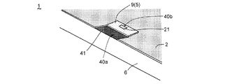
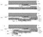
本発明の一実施形態に係る有機ELデバイスの構成について、図1乃至図5を参照して説明する。本実施形態の有機ELデバイス1は、図1に示すように、第1の基板2と、第1の基板2上に形成された有機層3と、透光性を有する第2の基板6と、第2の基板6上に形成され、有機層3に正孔を供給する陽極層4と、を備える。第1の基板2は、有機層3に電子を供給する陰極層21と、この陰極層21を平滑化する平滑化層22と、平滑化層22の陰極層21とは反対側の面に設けられたバリア層23と、を有する。第1の基板2及び第2の基板6は、有機層3及び陽極層4が当接するように、且つ陰極層21と陽極層4とが接しないように、接着層5を介して接合される。なお、陰極層21を第1の電極層とした場合、陽極層4は第2の電極層に相当する。
A configuration of an organic EL device according to an embodiment of the present invention will be described with reference to FIGS. As shown in FIG. 1, the
有機層3は、第1の基板2側から順に、電子注入層31と、発光層32と、ホール輸送層33と、ホール注入層34と、から構成される。陽極層4は、有機層3と当接する主電極部41と、主電極部41と接すると共に、有機層3とは絶縁層7によって絶縁された補助電極部42と、から構成される。接着層5は、吸湿層8を含み、この吸湿層8は、絶縁層7の外周に位置するように、第1の基板2及び第2の基板6間に挟持される。
The
有機層3は、第1の基板2の周縁部のいずれかの辺には形成されていない。本例においては、図2の(B)線及び(C)線で示す部分には、有機層3が形成されていない。この有機層3が形成されていない領域は、第1の基板2の4辺のいずれかに設けられていればよく、また、一辺の全長に亘って設けられていなくてもよく、部分的に設けられていてもよい(不図示)。一方、図2の(A)線及び(D)線で示す部分には、有機層3が端部まで形成されている(図3(a)も参照)。なお、本実施形態の有機ELデバイス1の製造工程において、第1の基板2に対して有機層3がロールツーロール方式で形成される場合、ロール進行方向は、図2の(A)線及び(D)線方向となる。図2の(A)線及び(D)線で示す部分を含む両辺には、有機層3等を封止すると共に、有機ELデバイス1の側部を保護する保持部材(不図示)が設けられる。この保持部材は、図2の(B)線及び(C)線で示す部分を含む両辺にも設けられてもよい。
The
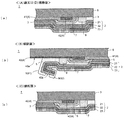
第2の基板6において、有機層3が形成されていない領域に対応する部分のいずれか、すなわち本例では、図2の(B)線で示す部分には、補助電極部42が有機層3のある領域より外周側へ延設されている(図1参照)。そして、この延設された補助電極部42と対向する第1の基板2の一部が、図3(b)及び図4に示すように、第2の基板6とは反対側に折り返されて、第1の基板2の裏面側に露出して、陰極取出し部40bを構成する。また、このとき、延設された補助電極部42が、第1の基板2の裏面側に露出して、陽極取出し部40aを構成する。陰極取出し部40bを第1の電極取出し部とした場合、陽極取出し部40aが第2の電極取出し部に相当する。図2の(C)線で示す部分には、図3(c)に示すように、補助電極部42が延設されていない。なお、本実施形態においては、陽極取出し部40a及び陰極取出し部40bが夫々1箇所に形成された例を示すが、2箇所以上に設けられてもよい。陰極取出し部40bは、陰極層21の一部を除いて封止材9によって封止され、図4に示すように、封止されていない部分が、第1の基板2の裏面側に露出する。この露出した補助電極部42及び陰極層21の一部に、外部給電端子等に電気的に接続される。なお、これら陽極取出し部40a及び陰極取出し部40bの形成手順については後述する。
In the
第1の基板2を構成する陰極層21には、アルミニウム、銅、ステンレス、ニッケル、錫、鉛、金、銀、鉄又はチタン等の金属又は合金等から成るシート材が用いられ、このシート材は、ロール巻取りが可能な程度の可撓性を有するものが好ましい。なお、陰極層21は、有機層3へ電子を供給するため、仕事関数の小さい金属、合金、導電性化合物又はこれらの混合物から成る電極材料から構成されることが好ましい。シート材の表面は、素子の短絡を抑制するため、平滑性を有することが必要であり、その表面粗さは、Ra100nm以下であることが好ましく、Ra10nm以下であることが更に好ましい。
For the
また、陰極層21には、アルミニウムや銀等の金属、又はこれら金属を含む化合物を用いることができ、アルミニウムと他の電極材料とを組み合わせて、積層構造等として構成されたものを用いてもよい。このような電極材料の組み合わせとしては、アルカリ金属とアルミニウムとの積層体、アルカリ金属と銀との積層体、アルカリ金属のハロゲン化物とアルミニウムとの積層体、アルカリ金属の酸化物とアルミニウムとの積層体、アルカリ土類金属や希土類金属とアルミニウムとの積層体、これらの金属種と他の金属との合金等が挙げられる。具体的には、ナトリウム、ナトリウム−カリウム合金、リチウム、マグネシウム等とアルミニウムとの積層体、マグネシウム−銀混合物、マグネシウム−インジウム混合物、アルミニウム−リチウム合金、フッ化リチウム(LiF)/アルミニウム混合物/積層体、アルミニウム/酸化アルミニウム(Al2O3)混合物等が挙げられる。
Further, the
平滑化層22には、例えば、熱硬化性ポリイミド樹脂、エポキシ樹脂、フェノール樹脂、メラミン樹脂、尿素樹脂、不飽和ポリエステル樹脂、アルキド樹脂 、ポリウレタン等から成る熱硬化性樹脂や、ポリエチレン、ポリプロピレン、ポリ塩化ビニル、ポリ塩化ビニリデン、ポリスチレン、ポリ酢酸ビニル、ABS樹脂、AS樹脂、アクリル樹脂等の熱可塑性樹脂や、ポリアミド、ナイロン、ポリアセタール、ポリカーボネート、変性ポリフェニレンエーテル、ポリブチレンテレフタレート、ポリエチレンテレフタレート等の樹脂等が用いられる。上記樹脂を含む溶液を金属箔上に塗布する、又は上記樹脂を陰極層21を構成するシート材と加熱ラミネートにより接合する等によって、陰極層21を平滑化することができる。平滑化層22によって第1の基板2が平滑化されるので、第1基板2上に形成される有機層3を、塗布等の方法によって均一な膜に仕上げることが容易となり、膜厚及び膜抵抗が均一で、輝度ムラの少ないELデバイスを実現することができる。
For the
バリア層23には、水分やガス等に対するバリア性を有する樹脂又は金属材料から構成され、汎用のバリアフィルム又は凹凸金属箔等は用いられる。このバリア層23によって、平滑化層22及び陰極層21に対して、水分やガス等が浸透することを抑制することができ、これら水分やガス等による有機層3の劣化を抑制することができる。
The
有機層3を構成する電子注入層31としては、陰極層21を構成する材料と共通のもの、酸化チタン、酸化亜鉛等の金属酸化物、上記材料を含めて、電子注入を促進させるドーパントを混合した有機半導体材料等が用いられる。また、発光層32としては、有機EL素子の発光材料として知られる任意の材料が用いられる。このような発光材料としては、例えば、アントラセン、ナフタレン、ピレン、テトラセン、コロネン、ペリレン、フタロペリレン、ナフタロペリレン、ジフェニルブタジエン、テトラフェニルブタジエン、クマリン、オキサジアゾール、ビスベンゾキサゾリン、ビススチリル、シクロペンタジエン、クマリン、オキサジアゾール、ビスベンゾキサゾリン、ビススチリル、シクロペンタジエン、キノリン金属錯体、トリス(8−ヒドロキシキノリナート)アルミニウム錯体、トリス(4−メチル−8−キノリナート)アルミニウム錯体、トリス(5−フェニル−8−キノリナート)アルミニウム錯体、アミノキノリン金属錯体、ベンゾキノリン金属錯体、トリ−(p−ターフェニル−4−イル)アミン、ピラン、キナクリドン、ルブレン、及びこれらの誘導体、あるいは、1−アリール−2,5−ジ(2−チエニル)ピロール誘導体、ジスチリルベンゼン誘導体、スチリルアリーレン誘導体、スチリルアミン誘導体、及びこれらの発光性化合物から成る基を分子の一部分に有する化合物あるいは高分子等が挙げられる。また、上記化合物に代表される蛍光色素由来の化合物のみならず、いわゆる燐光発光材料、例えば、Ir錯体、Os錯体、Pt錯体、ユーロピウム錯体等々の発光材料、又はそれらを分子内に有する化合物、若しくは高分子も好適に用いることができる。また、これらの材料から成る発光層32は、蒸着、転写等乾式プロセスによって成膜しても良いし、スピンコート、スプレーコート、ダイコート、グラビア印刷等、塗布によって成膜するものであってもよい。
As the
ホール輸送層33は、例えば、ホール輸送性を有する化合物の群から選定することができる。この種の化合物としては、例えば、4,4’−ビス[N−(ナフチル)−N−フェニル−アミノ]ビフェニル(α−NPD)、N,N’−ビス(3−メチルフェニル)−(1,1’−ビフェニル)−4,4’−ジアミン(TPD)、2−TNATA、4,4’,4”−トリス(N−(3−メチルフェニル)N−フェニルアミノ)トリフェニルアミン(MTDATA)、4,4’−N,N’−ジカルバゾールビフェニル(CBP)、スピロ−NPD、スピロ−TPD、スピロ−TAD、TNB等を代表例とする、トリアリールアミン系化合物、カルバゾール基を含むアミン化合物、フルオレン誘導体を含むアミン化合物等を挙げることができるが、一般に知られる任意のホール輸送材料を用いることができる。ホール注入層34は、例えは、銅フタロシアニン(CuPc)等の低分子量の有機化合物や、チオフェントリフェニルメタン、ヒドラゾリン、アリールアミン、ヒドラゾン、スチルベン、トリフェニルアミン等を含む有機材料が挙げられる。具体的には、ポリビニルカルバゾール(PVCz)、ポリエチレンジオキシチオフェン:ポリスチレンスルホネート(PEDOT:PSS)、TPD等の芳香族アミン誘導体等で、上記材料を単独で用いてもよく、また、二種類以上の材料を組み合わせて用いてもよい。
The
陽極層4の主電極部41には、有機EL素子の陽極材料として知られる任意の材料を用いることができる。陽極材料としては、銀、インジウム−錫酸化物(ITO)、インジウム−亜鉛酸化物(IZO)、錫酸化物、金等の金属のナノワイヤー、ナノドットを含むナノ粒子、導電性高分子、導電性の有機材料、ドーパント(ドナー又はアクセプタ)含有有機層、導電体と導電性有機材料(高分子含む)の混合物が挙げられ、導電性及び透光性を有していればよく、これらに限定されない。また、導電性物質の他にバインダーを含んだものであってもよい。バインダーとしては、アクリル樹脂、ポリエチレン、ポリプロピレン、ポリエチレンテレフタレート、ポリメチルメタクリレート、ポリスチレン、ポリエーテルスルホン、ポリアリレート、ポリカーボネート樹脂、ポリウレタン、ポリアクリルニトリル、ポリビニルアセタール、ポリアミド、ポリイミド、ジアクリルフタレート樹脂、セルロース系樹脂、ポリ塩化ビニル、ポリ塩化ビニリデン、ポリ酢酸ビニル、その他の熱可塑性樹脂や、これらの樹脂を構成する単量体の2種以上の共重合体が挙げられる。
For the
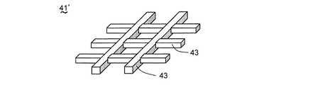
また、主電極部41は、図5に示すように、低抵抗性を有する細線材43を格子状、ライン状又はハニカム状に配置した、いわゆるグリッド電極41’から構成されたものであってもよい。細線材43の径は、主電極部41の透光性を低下させ難いように、100μm以下であることが好ましい。また、図示したような、細線材43が格子状に配置されたものの場合、各細線材43の間隔は、導電性を維持できる範囲で広く設定され、好ましくは、開口率が90%以上となるように設定される。細線材43としては、銀、アルミニウム、銅、ニッケル、錫、鉛、金、チタン等の各種金属及び合金、カーボン等の導電性材料が挙げられる。グリッド電極41’は、上記金属又は導電性材料を含むペーストをスクリーン印刷やグラビアコート、ダイコート等により、有機層3上にパターン形成される。このグリッド電極41’は、塗布による膜成形が容易であり、有機ELデバイス1を効率的に製造する上で有効である。なお、これらの材用や形成方法は、有機層3への濡れ性や、有機層3へのダメージを発生させないものであれば、特に限定されない。
Further, as shown in FIG. 5, the
補助電極部42は、対向する有機層3の周縁を囲うように枠状に配置されると共に、有機層3が形成されていない領域に対応する部分において、陰極層21との間に絶縁層7を介して、有機層のある領域より外周側に延設される。そして、この延設された部分が陽極取出し部40aを構成する。補助電極部42は、第2の基板6上に、上述した形状となるようにパターニング形成され、補助電極部42の枠状となった部分の上に、絶縁層7が配される。すなわち、発光層32と対向する主電極部41に透明性の高い材料を用い、周囲の補助電極部42に導電性の高い材料を用いれば、陽極層4全体としては、透光性が高く、且つ導電性も高くすることができる。補助電極部42の構成材料としては、一般的な配線電極に用いられる各種金属が用いられ、主電極部41との電気伝導性が良いものであれば、特に限定されない。また、主電極部41とは異なり、透光性を有していなくてもよい。
The
接着層5は、第1の基板2及び絶縁層7との接着性に優れた樹脂材から成るペースト状又はシート状の部材が、有機層3及び陽極層4の周縁を覆うように配置されたものである。接着層5の構成材料としては、例えば、シリコーン樹脂、フッ素樹脂、アクリル樹脂、ポリエチレン、ポリプロピレン、ポリエチレンテレフタレート、ポリメチルメタクリレート、ポリスチレン、ポリ酢酸ビニル等が挙げられる。
The
第2の基板6は、第1の基板2と同形状に形成された透明な板状部材であり、板厚が均一で、表面平滑性を有するものが用いられる。第2の基板6の構成材料としては、例えば、ソーダライムガラスや無アルカリガラス等の透光性ガラスや、透光性樹脂材料等が用いられる。
The
絶縁層7は、補助電極部42の枠状部分と略相似形状で、補助電極部42よりも幅広となるようにパターン形成されたものである。絶縁層7は、その内周縁が有機層3の外周よりも大きくなるようパターンニングされ、補助電極部42と有機層3との間の絶縁性を確保する。絶縁層7の構成材料としては、熱硬化性ポリイミド樹脂、エポキシ樹脂等から成る熱硬化性樹脂や、ポリエチレン、ポリプロピレン等の熱可塑性樹脂をウェットプロセスにより形成するか、SiOやSiN等の酸化物や窒化物をスパッタ等のドライプロセスで形成することができる。なお、何れのプロセスにおいてもパターニングが必要であり、特にウェットプロセスとしては、好ましくはスクリーン印刷、ダイコート、スプレーコート、グラビアコート等の方法によって絶縁層7を形成することができる。
The insulating
吸湿層8は、乾燥剤を含有させた樹脂材料を、有機層3が形成される領域が開口するよう枠状にパターン形成されたものである。この吸湿層8を設けることにより、接着層5に僅かに侵入した水分がブロックされるので、有機層3の劣化を効果的に抑制することができる。吸湿層8の構成材料には、例えば、エポキシ系樹脂、アクリル系樹脂、シリコーン系樹脂等から成る光硬化型接着性樹脂に、酸化カルシウム、酸化バリウム、酸化ナトリウム、酸化カリウム、硫酸ナトリウム、硫酸カルシウム、硫酸マグネシウム、塩化カルシウム、塩化マグネシウム、塩化銅、酸化マグネシウム等から成る乾燥剤が添加されたものを用いることができる。なお、吸湿層8は、第2の基板6と第1の基板2とが接合される前に、予め第2の基板6のうち、第1の基板2と向かい合う面に設けられていることが好ましい。
The
封止材9は、補助電極部42の露出から陰極取出し部40bの折り返し位置までの領域を封止する基部側封止部91と、第1の電極取出し部40における陰極層21、平滑化層22及びバリア層23の端部を封止する端部封止部92とを含む(図3(b)参照)。基部側封止部91は、第1の基板2と第2の基板6とを接合する接着層5の一部が延設されたものである。また、端部封止部92は、上記端部を封止すると共に、この端部と第1の基板2のバリア層23とを接着する役割を果たす。このように、陰極取出し部40bが、陰極層21の一部を除いて封止材9によって封止されることにより、デバイス内に水分等が浸入し難くなり、有機層3の劣化を抑制することができる。なお、後述するように、封止材9は、接着層5とは別部材であってもよい。封止材9の材料には、接着層5と同様の材料が用いられる。なお、封止材9は、有機層3が形成される領域の外側、又は第1の基板2の裏側に配置されるので、透光性を有しない材料が用いられてもよい。
The sealing
次に、陽極取出し部40a及び陰極取出し部40bの形成手順について、図6(a)乃至(c)を参照して説明する。第1の基板2上には、図6(a)に示すように、有機層3が積層される。また、第2の基板6上には、補助電極部42、主電極部41及び絶縁層7が夫々所定の形状にパターン形成される。また、第1の基板2及び第2の基板6が、図6(b)に示すように、有機層3及び陽極層4(主電極部41)が当接するように配され、第2の基板6の所定位置には、吸湿層8が設けられ、これらが接着層5によって接着固定される。このとき、接着層5は、延設された補助電極部42の基端側に一部被り、先端側には被らないように配される。また、補助電極部42及び絶縁層7が枠状に構成され(図1参照)、これら補助電極部42及び絶縁層7が、積層されて他の部分より厚くなることにより、接着層5の有機層3側への流入を堰き止めるダムとして機能する。接合後、陰極層21、平滑化層22及びバリア層23の端部には、端部封止部92が設けられると共に、第1の基板2が、図6(c)に示すように、第2の基板6とは反対側に折り返され、端部封止部92によって第2の基板6の裏面(バリア層23)に固定される。なお、基部側封止部91に、延設された補助電極部42の基端側に一部被った接着層5を用いれば、封止材9を塗布する工程を一部簡略化することができる。以上の手順により、延設された補助電極部42が露出して、陽極取出し部40aが形成されると共に、延設された補助電極部42と対向する第1の基板2の陰極層21が、第1の基板2の裏面側に露出して、陰極取出し部40bが形成される。
Next, a procedure for forming the
すなわち、有機ELデバイス1は、延設された補助電極部42と対向する第1の基板2を折り返すことにより、陽極取出し部40a及び陰極取出し部40bを簡易に形成することができるので、効率的に製造することができる。しかも、第1の基板2において、陰極層21の裏面側に樹脂製の平滑化層22が用いられた場合でも、陰極取出し部40bを第1の基板2の裏面側に取出すことができる。また、第1の基板2、有機層3、絶縁層7、補助電極部42及び主電極部41を構成する材料には、可撓性を有する材料を用いることができ、また、第2の基板6は、可撓性又は硬質性のいずれを有するものであってもよい。つまり、可撓性を有するように作成された有機層3付の第1の基板6を、可撓性又は硬質性の適宜の第2の基板6に接合させれば、同一構成の有機層3付の第1の基板6を用いて、フレキシブル型及びハード型の両方の有機ELデバイス1を製造することができる。
That is, since the
また、本実施形態の有機ELデバイス1は、第1の基板2として、ロール状に巻かれた状態で供給される帯状のシート材を用いることもできる。この場合、帯状の第1の基板2の表面上に、有機層3をスリットコータ等によって連続的に形成し、形成後、再びロール状に巻き取り回収する。こうすれば、いわゆるロールツーロール方式により、複数の有機層3付の第1の基板6から成るシートロール(不図示)を作成することができる。そして、帯状の第1の基板2と同じ幅で、且つ同じ長さに形成され、陽極層4等が形成された長尺の第2の基板6に、このシートロールを接着し、これらを定間隔で裁断すると共に、上述したように、第1の基板2を除去して、陽極取出し部40a及び陰極取出し部40bを形成する。こうすれば、図2に示したような有機ELデバイス1を、短時間で数多く製造することができる。特に、近年では、発光層32の複層化や、それらの間に電荷調整層を配置する等、有機層3が多層化される傾向にあり、ロールツーロール方式による有機層3の形成は、上述したような多数層から成る有機層を、同時に数多く製造することができる。
Moreover, the
次に、上述した陽極取出し部40aの形成手順とは別の手順について、図7(a)乃至(c)を参照して説明する。この手順は、まず、接着層5を、陽極取出し部40aの一部に延設させないように配置して、第1の基板2と第2の基板6とを接合させる(図7(a))。そして、陽極取出し部40aに相当する箇所を折り返し(図7(b))、折り返し後、接着層5とは別部材の封止材9’で、陰極取出し部40bを封止及び固定する(図7(c))。この手順によれば、第1の基板2と第2の基板6とが十分に接着された後に、陰極取出し部40bに相当する箇所を折り返すことができるので、折り返しの動作によって接着層5と補助電極部42との間に隙間が形成され難くなり、接着層5への水分等の浸入を抑制することができる。
Next, a procedure different from the procedure for forming the
なお、本発明は、基板の周縁部のいずれかに有機層が形成されいない領域があり、この領域に配された電極層の一部が、折り返されることによって、電極取出し部として露出されているものであれば、上記実施形態に限らず、種々の変形が可能である。また、第1の基板6(陰極層21)、主電極部41又は補助電極部42等を構成する材料を適宜に選択することにより、上述した陰極及び陽極の機能を夫々逆にすることもできる。すなわち、第1の基板6側を陽極層として機能させ、主電極部41及び補助電極部42側を陰極層として機能させることもできる。
In the present invention, there is a region where the organic layer is not formed on any of the peripheral portions of the substrate, and a part of the electrode layer disposed in this region is folded back to be exposed as an electrode extraction portion. If it is a thing, not only the said embodiment but a various deformation | transformation is possible. In addition, by appropriately selecting materials constituting the first substrate 6 (cathode layer 21), the
1 有機ELデバイス
2 第1の基板
21 陰極層(第1の電極層)
22 平滑化層
23 バリア層
3 有機層
4 陽極層(第2の電極層)
40a 陰極取出し部(第2の電極取出し部)
40b 陽極取出し部(第1の電極取出し部)
41 主電極部
42 補助電極部
5 接着層
6 第2の基板
7 絶縁層
8 吸湿層
9 封止材
9’ 封止材
DESCRIPTION OF
22
40a Cathode extraction part (second electrode extraction part)
40b Anode extraction part (first electrode extraction part)
41
Claims (9)
前記第1の基板及び前記第2の基板は、前記有機層及び前記第2の電極層が当接するように、且つ前記第1の電極層と前記第2の電極層とが接しないように、接着層を介して接合され、
前記有機層は、前記第1の基板の周縁部のいずれかの領域には形成されておらず、
前記第2の電極層は、前記有機層の形成されていない領域に対応する部分において該有機層のある領域より外周側に延設されており、
前記延設された第2の電極層と対向する前記第1の基板の一部が、前記第2の基板とは反対側に折り返されて、第1の電極取出し部を構成すると共に、前記延設された第2の電極層が前記第1の基板から露出して、第2の電極取出し部を構成していることを特徴とする有機ELデバイス。 A first substrate having a first electrode layer and a smoothing layer for smoothing the first electrode layer; an organic layer formed on the first electrode layer of the first substrate; And a second electrode layer formed on the second substrate, and
In the first substrate and the second substrate, the organic layer and the second electrode layer are in contact with each other, and the first electrode layer and the second electrode layer are not in contact with each other. Bonded through an adhesive layer,
The organic layer is not formed in any region of the peripheral portion of the first substrate,
The second electrode layer extends from the region having the organic layer to the outer peripheral side in a portion corresponding to the region where the organic layer is not formed,
A portion of the first substrate facing the extended second electrode layer is folded back to the opposite side of the second substrate to form a first electrode extraction portion, and the extension An organic EL device, wherein a second electrode layer provided is exposed from the first substrate to constitute a second electrode extraction portion.
Priority Applications (3)
| Application Number | Priority Date | Filing Date | Title |
|---|---|---|---|
| JP2011037447A JP2012174607A (en) | 2011-02-23 | 2011-02-23 | Organic el device |
| PCT/JP2011/079202 WO2012114618A1 (en) | 2011-02-23 | 2011-12-16 | Organic el device |
| TW100148275A TW201244202A (en) | 2011-02-23 | 2011-12-23 | Organic electroluminescence device |
Applications Claiming Priority (1)
| Application Number | Priority Date | Filing Date | Title |
|---|---|---|---|
| JP2011037447A JP2012174607A (en) | 2011-02-23 | 2011-02-23 | Organic el device |
Publications (1)
| Publication Number | Publication Date |
|---|---|
| JP2012174607A true JP2012174607A (en) | 2012-09-10 |
Family
ID=46720420
Family Applications (1)
| Application Number | Title | Priority Date | Filing Date |
|---|---|---|---|
| JP2011037447A Withdrawn JP2012174607A (en) | 2011-02-23 | 2011-02-23 | Organic el device |
Country Status (3)
| Country | Link |
|---|---|
| JP (1) | JP2012174607A (en) |
| TW (1) | TW201244202A (en) |
| WO (1) | WO2012114618A1 (en) |
Cited By (2)
| Publication number | Priority date | Publication date | Assignee | Title |
|---|---|---|---|---|
| JP2016009620A (en) * | 2014-06-25 | 2016-01-18 | パナソニック株式会社 | Organic EL element |
| JP2019200303A (en) * | 2018-05-16 | 2019-11-21 | 凸版印刷株式会社 | Dimming unit |
Family Cites Families (4)
| Publication number | Priority date | Publication date | Assignee | Title |
|---|---|---|---|---|
| JPH07130472A (en) * | 1993-11-04 | 1995-05-19 | Nippondenso Co Ltd | Electroluminescent element |
| JPH09129369A (en) * | 1995-10-31 | 1997-05-16 | Nippon Seiki Co Ltd | Electroluminescent element and manufacture thereof |
| JP2007280693A (en) * | 2006-04-04 | 2007-10-25 | Koizumi Lighting Technology Corp | El light source |
| US8576209B2 (en) * | 2009-07-07 | 2013-11-05 | Semiconductor Energy Laboratory Co., Ltd. | Display device |
-
2011
- 2011-02-23 JP JP2011037447A patent/JP2012174607A/en not_active Withdrawn
- 2011-12-16 WO PCT/JP2011/079202 patent/WO2012114618A1/en active Application Filing
- 2011-12-23 TW TW100148275A patent/TW201244202A/en unknown
Cited By (3)
| Publication number | Priority date | Publication date | Assignee | Title |
|---|---|---|---|---|
| JP2016009620A (en) * | 2014-06-25 | 2016-01-18 | パナソニック株式会社 | Organic EL element |
| JP2019200303A (en) * | 2018-05-16 | 2019-11-21 | 凸版印刷株式会社 | Dimming unit |
| JP7206633B2 (en) | 2018-05-16 | 2023-01-18 | 凸版印刷株式会社 | dimming unit |
Also Published As
| Publication number | Publication date |
|---|---|
| WO2012114618A1 (en) | 2012-08-30 |
| TW201244202A (en) | 2012-11-01 |
Similar Documents
| Publication | Publication Date | Title |
|---|---|---|
| US9054334B2 (en) | Organic EL device | |
| JP5842089B2 (en) | Organic EL device | |
| JPWO2011074633A1 (en) | Organic electroluminescence device | |
| JP6021020B2 (en) | Organic electroluminescence device | |
| JP5735819B2 (en) | Organic electroluminescence device | |
| JP2010157424A (en) | Organic el light-emitting device | |
| JP5613590B2 (en) | Organic EL device | |
| WO2012121254A1 (en) | Planar light emitting device and manufacturing method thereof | |
| WO2013146350A1 (en) | Light emitting apparatus and method for manufacturing light emitting apparatus | |
| WO2016013160A1 (en) | Light emitting device | |
| WO2012121249A1 (en) | Planar light emitting device | |
| WO2012114618A1 (en) | Organic el device | |
| JP5842088B2 (en) | Organic EL device and method for manufacturing organic EL device | |
| WO2012121251A1 (en) | Planar light emitting device | |
| WO2012120746A1 (en) | Organic el device | |
| JP2012212555A (en) | Light-emitting device | |
| JP2013191276A (en) | Organic electroluminescent element | |
| JP2013030335A (en) | Organic electroluminescent element | |
| WO2012132823A1 (en) | Light-emitting device |
Legal Events
| Date | Code | Title | Description |
|---|---|---|---|
| A300 | Application deemed to be withdrawn because no request for examination was validly filed |
Free format text: JAPANESE INTERMEDIATE CODE: A300 Effective date: 20140513 |