JP2012168899A - Voltage regulator - Google Patents
Voltage regulator Download PDFInfo
- Publication number
- JP2012168899A JP2012168899A JP2011031297A JP2011031297A JP2012168899A JP 2012168899 A JP2012168899 A JP 2012168899A JP 2011031297 A JP2011031297 A JP 2011031297A JP 2011031297 A JP2011031297 A JP 2011031297A JP 2012168899 A JP2012168899 A JP 2012168899A
- Authority
- JP
- Japan
- Prior art keywords
- voltage
- output
- voltage regulator
- limiting circuit
- output transistor
- Prior art date
- Legal status (The legal status is an assumption and is not a legal conclusion. Google has not performed a legal analysis and makes no representation as to the accuracy of the status listed.)
- Pending
Links
Images


Classifications
-
- G—PHYSICS
- G05—CONTROLLING; REGULATING
- G05F—SYSTEMS FOR REGULATING ELECTRIC OR MAGNETIC VARIABLES
- G05F1/00—Automatic systems in which deviations of an electric quantity from one or more predetermined values are detected at the output of the system and fed back to a device within the system to restore the detected quantity to its predetermined value or values, i.e. retroactive systems
- G05F1/10—Regulating voltage or current
- G05F1/46—Regulating voltage or current wherein the variable actually regulated by the final control device is dc
- G05F1/56—Regulating voltage or current wherein the variable actually regulated by the final control device is dc using semiconductor devices in series with the load as final control devices
-
- G—PHYSICS
- G05—CONTROLLING; REGULATING
- G05F—SYSTEMS FOR REGULATING ELECTRIC OR MAGNETIC VARIABLES
- G05F3/00—Non-retroactive systems for regulating electric variables by using an uncontrolled element, or an uncontrolled combination of elements, such element or such combination having self-regulating properties
- G05F3/02—Regulating voltage or current
- G05F3/08—Regulating voltage or current wherein the variable is dc
- G05F3/10—Regulating voltage or current wherein the variable is dc using uncontrolled devices with non-linear characteristics
- G05F3/16—Regulating voltage or current wherein the variable is dc using uncontrolled devices with non-linear characteristics being semiconductor devices
- G05F3/20—Regulating voltage or current wherein the variable is dc using uncontrolled devices with non-linear characteristics being semiconductor devices using diode- transistor combinations
Abstract
Description
本発明は、ボルテージレギュレータのオーバーシュート特性の改善に関する。 The present invention relates to an improvement in overshoot characteristics of a voltage regulator.
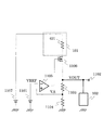
従来のボルテージレギュレータは、図11のブロック図に示すように、基準電圧回路1101と、分圧抵抗1103及び1104と、エラーアンプ1105と、出力トランジスタ1106と、から構成されている。
As shown in the block diagram of FIG. 11, the conventional voltage regulator includes a
基準電圧回路1101は、基準電圧VREFを出力する。分圧抵抗1103及び1104は、ボルテージレギュレータの出力端子1102の出力電圧VOUTを分圧し、分圧電圧VAを出力する。エラーアンプ1105は、基準電圧VREFと分圧電圧VAとの差電圧を増幅するし、出力電圧VERRによって出力トランジスタ1106のゲートを制御する。出力トランジスタ1106は、電圧源1107の電源電圧VDDと出力電圧VERRによって、出力端子1102の出力電圧VOUTを一定に保つ。ボルテージレギュレータは、電源電圧VDDにより動作する。
The
ボルテージレギュレータは、以下のように動作して出力電圧VOUTを一定に保つ(例えば、特許文献1参照)。 The voltage regulator operates as follows to keep the output voltage VOUT constant (see, for example, Patent Document 1).
出力電圧VOUTが低くなると、エラーアンプ1105の出力電圧VERRが低くなり、出力トランジスタ1106のゲート・ソース間電圧は大きくなる。従って、出力トランジスタ1106のON抵抗が小さくなり、出力電圧VOUTは高くなる。出力電圧VOUTが高くなると、エラーアンプ1105の出力電圧VERRが高くなり、出力トランジスタ1106のゲート・ソース間電圧は小さくなる。従って、出力トランジスタ1106のON抵抗が大きくなり、出力電圧VOUTは低くなる。
When the output voltage VOUT decreases, the output voltage VERR of the
しかし、従来のボルテージレギュレータでは、電源起動時や電源変動時など電源電圧VDDがパルス的に変化したときや、ボルテージレギュレータの出力端子1102に接続された負荷が急激に変化したときに、出力電圧VOUTにオーバーシュートが発生するといった問題点があった。
However, in the conventional voltage regulator, the output voltage VOUT is changed when the power supply voltage VDD changes in pulses, such as when the power supply is started or when the power supply fluctuates, or when the load connected to the
本発明は、上記の様な問題点を解決するために考案されたものであり、オーバーシュート特性を改善したボルテージレギュレータを実現するものである。 The present invention has been devised to solve the above-described problems, and realizes a voltage regulator with improved overshoot characteristics.
本発明のボルテージレギュレータは、基準電圧回路と、前記基準電圧回路の基準電圧に基づいた出力電圧を出力する出力端子と、前記出力電圧を分圧する分圧回路と、出力トランジスタと、前記分圧回路の出力と、前記基準電圧に基づいて、前記出力トランジスタの制御信号を出力するエラーアンプと、を有するボルテージレギュレータであって、前記ボルテージレギュレータは、更に、電圧制限回路と、電流制限回路と、を有することを特徴とするボルテージレギュレータ、とした。 The voltage regulator of the present invention includes a reference voltage circuit, an output terminal that outputs an output voltage based on a reference voltage of the reference voltage circuit, a voltage dividing circuit that divides the output voltage, an output transistor, and the voltage dividing circuit And an error amplifier that outputs a control signal for the output transistor based on the reference voltage, wherein the voltage regulator further includes a voltage limiting circuit and a current limiting circuit. It was set as the voltage regulator characterized by having.
本発明のボルテージレギュレータによれば、出力電圧の過大なオーバーシュートを起こさず動作させることが可能となり、オーバーシュート特性を改善したボルテージレギュレータを提供することが出来る。 According to the voltage regulator of the present invention, it is possible to operate without causing an excessive overshoot of the output voltage, and it is possible to provide a voltage regulator with improved overshoot characteristics.
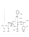
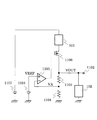
図1は、本実施形態のボルテージレギュレータを示すブロック図である。
本実施形態のボルテージレギュレータは、基準電圧回路1101と、分圧抵抗1103及び1104と、エラーアンプ1105と、出力トランジスタ1106と、電流制限回路101と、電圧制限回路102と、を備えている。
FIG. 1 is a block diagram showing the voltage regulator of this embodiment.
The voltage regulator of this embodiment includes a
電流制限回路101は、電圧源1107と出力トランジスタ1106の間に設けられている。電圧制限回路102は、出力端子1102と接地端子の間に設けられている。
The current limiting
電流制限回路101は、出力トランジスタ1106が流す電流の最大値を制限する機能を備えている。電流制限回路101は、例えば、図2に示す定電流源201とトランジスタ202及び203からなるカレントミラー回路に依るものや、図3に示すデプレッション型のトランジスタ301に依るものや、図4に示す抵抗401に依るもので、構成される。
The current limiting
電圧制限回路102は、出力電圧VOUTが所望の電圧より高くなると、インピーダンスが小さくなる。電圧制限回路102は、例えば、図5に示す様なダイオード501と基準電圧回路502(基準電圧回路502は、ダイオードであっても良い)に依るものや、図6に示すような飽和接続されたトランジスタ601に依るもので、構成される。
When the output voltage VOUT is higher than a desired voltage, the
以下に、本実施形態のボルテージレギュレータの動作について説明する。
電源起動時や電源変動時などの電源電圧VDDがパルス的に変化しとき、またはボルテージレギュレータの出力端子1102に接続された負荷が急激に変化したときに、電圧カップリングの影響や、出力トランジスタ1106の負荷への電流供給能力を超えることなどで、出力電圧VOUTが低下する。出力電圧VOUTを分圧する分圧電圧VAも低下するので、エラーアンプ1105の出力電圧VERRが低くなる。従って、出力トランジスタ1106は、ON抵抗が小さくなるので、瞬時に大きな電流を流そうとする。
The operation of the voltage regulator of this embodiment will be described below.
When the power supply voltage VDD changes in pulses, such as when the power supply is started or when the power supply fluctuates, or when the load connected to the
このとき、出力トランジスタ1106と電圧源1107の間に設けられた電流制限回路101に依って、出力トランジスタ1106の駆動電流は制限される。例えば、図2の電流制限回路101の場合は、電流源201が流す電流を制限する。
At this time, the drive current of the
また、出力トランジスタ1106の駆動電流が増加すると、出力電圧VOUTも高くなる。このとき、出力端子1102に設けられた電圧制限回路102によって、出力電圧VOUTは制限される。例えば、図5の電圧制限回路102の場合は、出力端子1102と接地端子の間に順バイアス接続したダイオード501によって、出力端子1102の電圧が大きくなるとインピーダンスが小さくなる。更に、出力トランジスタ1106の駆動電流はダイオード501によっても制限されるので、出力電圧VOUTは過大なオーバーシュートを起こさず動作させることが可能となる。
As the drive current of the
従って、本実施形態のボルテージレギュレータは、出力電圧の過大なオーバーシュートを起こさず動作させることが可能となり、オーバーシュート特性を改善したボルテージレギュレータを提供することが出来る。 Therefore, the voltage regulator of this embodiment can be operated without causing an excessive overshoot of the output voltage, and a voltage regulator with improved overshoot characteristics can be provided.
本実施形態のボルテージレギュレータでは、分圧抵抗1103、分圧抵抗1104によって、出力電圧VOUTを分圧するものとして説明したが、これらの抵抗値は、ゼロまたは過大な値として構成しても、所望の分圧比が得られれば、同様の効果が得られる。
In the voltage regulator according to the present embodiment, the output voltage VOUT is divided by the voltage dividing
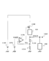
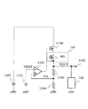
本実施形態のボルテージレギュレータでは、電流制限回路101が出力トランジスタ1106にとってハイサイドに設けられているとして説明したが、図7及び図8に示すようにロウサイドに設けられても同様の効果が得られる。図8は、電流制限回路101をデプレッション型トランジスタ801で構成した例を示したものである。図8において、出力電圧VOUTが高くなるほど、デプレッション型トランジスタ801はバックゲート電圧降下により閾値電圧が高くなり、電流をより制限するように動作する。従って、ボルテージレギュレータが安定動作しているときは、出力トランジスタ1106の駆動電流を大きくし、出力電圧VOUTが高くなったときのみ、電流をより制限することが出来るといった、更なるメリットが得られる。
In the voltage regulator according to this embodiment, the current limiting
本実施形態のボルテージレギュレータでは、電流制限回路101が、図2、図3、図4、図7に示すようなものとして説明したが、同様の機能を有することが可能な、その他の構成でも同様な効果が得られる。
In the voltage regulator of this embodiment, the current limiting
本実施形態のボルテージレギュレータでは、電圧制限回路102が、図5、図6に示す様なものとして説明したが、これらを構成するダイオードまたはトランジスタは、出力電圧VOUTによって、適切に直列させても良い。また、同様の機能を有することが可能な、その他の構成でも同様な効果が得られる。例えば、ダイオードの代わりに、ダイオード接続させたトランジスタを設けても良い。
In the voltage regulator of the present embodiment, the
本実施形態のボルテージレギュレータでは、出力トランジスタがP型であるとして説明したが、N型であるとしても同様な効果が得られる。この場合のブロック図の例を図9及び図10に示す。出力トランジスタは、エンハンスメント型であるか、デプレッション型であるか、その形態は限定されない。 In the voltage regulator of the present embodiment, the output transistor is described as being P-type, but the same effect can be obtained even if it is N-type. Examples of block diagrams in this case are shown in FIGS. Whether the output transistor is an enhancement type or a depletion type is not limited.
101 電流制限回路
102 電圧制限回路
201 電流源
502、1101 基準電圧回路
1105 エラーアンプ
101
Claims (4)
前記出力トランジスタと直列に接続された、前記出力トランジスタの出力電流を制限する電流制限回路を備えたことを特徴とするボルテージレギュレータ。 A voltage regulator having an error amplifying circuit for controlling a gate of the output transistor by amplifying a difference between a divided voltage obtained by dividing an output voltage of the output transistor and a reference voltage,
A voltage regulator comprising: a current limiting circuit that limits the output current of the output transistor connected in series with the output transistor.
Priority Applications (5)
| Application Number | Priority Date | Filing Date | Title |
|---|---|---|---|
| JP2011031297A JP2012168899A (en) | 2011-02-16 | 2011-02-16 | Voltage regulator |
| CN2012100298492A CN102645945A (en) | 2011-02-16 | 2012-02-10 | Voltage regulator |
| TW101104525A TWI525413B (en) | 2011-02-16 | 2012-02-13 | Stabilizer |
| US13/372,007 US8884594B2 (en) | 2011-02-16 | 2012-02-13 | Voltage regulator |
| KR1020120014891A KR20120094435A (en) | 2011-02-16 | 2012-02-14 | Voltage regulator |
Applications Claiming Priority (1)
| Application Number | Priority Date | Filing Date | Title |
|---|---|---|---|
| JP2011031297A JP2012168899A (en) | 2011-02-16 | 2011-02-16 | Voltage regulator |
Publications (2)
| Publication Number | Publication Date |
|---|---|
| JP2012168899A true JP2012168899A (en) | 2012-09-06 |
| JP2012168899A5 JP2012168899A5 (en) | 2014-01-30 |
Family
ID=46636389
Family Applications (1)
| Application Number | Title | Priority Date | Filing Date |
|---|---|---|---|
| JP2011031297A Pending JP2012168899A (en) | 2011-02-16 | 2011-02-16 | Voltage regulator |
Country Status (5)
| Country | Link |
|---|---|
| US (1) | US8884594B2 (en) |
| JP (1) | JP2012168899A (en) |
| KR (1) | KR20120094435A (en) |
| CN (1) | CN102645945A (en) |
| TW (1) | TWI525413B (en) |
Cited By (3)
| Publication number | Priority date | Publication date | Assignee | Title |
|---|---|---|---|---|
| TWI628889B (en) * | 2013-08-26 | 2018-07-01 | 日商艾普凌科有限公司 | Voltage regulator |
| CN110297515A (en) * | 2018-03-22 | 2019-10-01 | 艾普凌科有限公司 | Voltage regulator |
| KR20230097500A (en) * | 2021-12-24 | 2023-07-03 | 한국전자기술연구원 | Constant current supply circuit applying the replica bias scheme and adaptive current compensation method thereof |
Families Citing this family (9)
| Publication number | Priority date | Publication date | Assignee | Title |
|---|---|---|---|---|
| US9018924B2 (en) | 2012-09-14 | 2015-04-28 | Nxp B.V. | Low dropout regulator |
| CN103092245B (en) * | 2013-01-09 | 2014-08-20 | 卓捷创芯科技(深圳)有限公司 | Ultra-low-power-consumption low dropout stabilized voltage supply circuit and radio frequency identification (RFID) tags |
| US9041367B2 (en) * | 2013-03-14 | 2015-05-26 | Freescale Semiconductor, Inc. | Voltage regulator with current limiter |
| CN103761953B (en) * | 2014-01-28 | 2016-04-06 | 北京京东方显示技术有限公司 | A kind of indicative control unit and display device |
| JP6513943B2 (en) * | 2014-12-19 | 2019-05-15 | エイブリック株式会社 | Voltage regulator |
| US9438101B1 (en) * | 2015-05-07 | 2016-09-06 | Qm Power, Inc. | High speed switching solid state relay circuit |
| US10250139B2 (en) * | 2016-03-31 | 2019-04-02 | Micron Technology, Inc. | Apparatuses and methods for a load current control circuit for a source follower voltage regulator |
| JP7075172B2 (en) * | 2017-06-01 | 2022-05-25 | エイブリック株式会社 | Reference voltage circuit and semiconductor device |
| US10496115B2 (en) * | 2017-07-03 | 2019-12-03 | Macronix International Co., Ltd. | Fast transient response voltage regulator with predictive loading |
Citations (4)
| Publication number | Priority date | Publication date | Assignee | Title |
|---|---|---|---|---|
| JPS5653217U (en) * | 1979-09-29 | 1981-05-11 | ||
| JPH06309050A (en) * | 1993-04-26 | 1994-11-04 | Matsushita Electron Corp | Semiconductor device |
| JP2006155357A (en) * | 2004-11-30 | 2006-06-15 | Sanyo Electric Co Ltd | Voltage lowering circuit |
| JP2008217203A (en) * | 2007-03-01 | 2008-09-18 | Sanyo Electric Co Ltd | Regulator circuit |
Family Cites Families (10)
| Publication number | Priority date | Publication date | Assignee | Title |
|---|---|---|---|---|
| DE3030620A1 (en) * | 1980-08-13 | 1982-03-11 | Siemens AG, 1000 Berlin und 8000 München | ARRANGEMENT FOR CHANGING THE ELECTRICAL CIRCUIT CONFIGURATION OF INTEGRATED SEMICONDUCTOR CIRCUITS |
| DE3341345A1 (en) * | 1983-11-15 | 1985-05-23 | SGS-ATES Deutschland Halbleiter-Bauelemente GmbH, 8018 Grafing | VOLTAGE REGULATOR |
| JP2706720B2 (en) | 1990-11-28 | 1998-01-28 | セイコーインスツルメンツ株式会社 | Voltage regulator |
| JP3668612B2 (en) * | 1998-06-29 | 2005-07-06 | 株式会社東芝 | Optical semiconductor device drive circuit and optical transceiver module |
| JP3818231B2 (en) * | 2002-07-12 | 2006-09-06 | 株式会社デンソー | Power circuit |
| ITTO20030533A1 (en) * | 2003-07-10 | 2005-01-11 | Atmel Corp | PROCEDURE AND CIRCUIT FOR CURRENT LIMITATION IN |
| JP4443301B2 (en) * | 2004-05-17 | 2010-03-31 | セイコーインスツル株式会社 | Voltage regulator |
| JP4689473B2 (en) * | 2005-05-16 | 2011-05-25 | シャープ株式会社 | DC stabilized power supply circuit |
| JP5421133B2 (en) * | 2009-02-10 | 2014-02-19 | セイコーインスツル株式会社 | Voltage regulator |
| CN201638100U (en) * | 2010-02-03 | 2010-11-17 | 乌鲁木齐希望电子有限公司 | High efficiency and low loss linear voltage-stabilizing and energy-saving device |
-
2011
- 2011-02-16 JP JP2011031297A patent/JP2012168899A/en active Pending
-
2012
- 2012-02-10 CN CN2012100298492A patent/CN102645945A/en active Pending
- 2012-02-13 US US13/372,007 patent/US8884594B2/en not_active Expired - Fee Related
- 2012-02-13 TW TW101104525A patent/TWI525413B/en active
- 2012-02-14 KR KR1020120014891A patent/KR20120094435A/en not_active Application Discontinuation
Patent Citations (4)
| Publication number | Priority date | Publication date | Assignee | Title |
|---|---|---|---|---|
| JPS5653217U (en) * | 1979-09-29 | 1981-05-11 | ||
| JPH06309050A (en) * | 1993-04-26 | 1994-11-04 | Matsushita Electron Corp | Semiconductor device |
| JP2006155357A (en) * | 2004-11-30 | 2006-06-15 | Sanyo Electric Co Ltd | Voltage lowering circuit |
| JP2008217203A (en) * | 2007-03-01 | 2008-09-18 | Sanyo Electric Co Ltd | Regulator circuit |
Cited By (4)
| Publication number | Priority date | Publication date | Assignee | Title |
|---|---|---|---|---|
| TWI628889B (en) * | 2013-08-26 | 2018-07-01 | 日商艾普凌科有限公司 | Voltage regulator |
| CN110297515A (en) * | 2018-03-22 | 2019-10-01 | 艾普凌科有限公司 | Voltage regulator |
| KR20230097500A (en) * | 2021-12-24 | 2023-07-03 | 한국전자기술연구원 | Constant current supply circuit applying the replica bias scheme and adaptive current compensation method thereof |
| KR102624225B1 (en) * | 2021-12-24 | 2024-01-15 | 한국전자기술연구원 | Constant current supply circuit applying the replica bias scheme and adaptive current compensation method thereof |
Also Published As
| Publication number | Publication date |
|---|---|
| TW201303541A (en) | 2013-01-16 |
| KR20120094435A (en) | 2012-08-24 |
| TWI525413B (en) | 2016-03-11 |
| US8884594B2 (en) | 2014-11-11 |
| CN102645945A (en) | 2012-08-22 |
| US20120206119A1 (en) | 2012-08-16 |
Similar Documents
| Publication | Publication Date | Title |
|---|---|---|
| JP2012168899A (en) | Voltage regulator | |
| JP4953246B2 (en) | Voltage regulator | |
| KR101898290B1 (en) | Voltage regulator | |
| US9857817B2 (en) | Sink/source output stage with operating point current control circuit for fast transient loading | |
| KR101586525B1 (en) | Voltage regulator | |
| US8665020B2 (en) | Differential amplifier circuit that can change current flowing through a constant-current source according to load variation, and series regulator including the same | |
| JP2018160289A (en) | Low dropout voltage regulator with floating voltage reference | |
| KR102255543B1 (en) | Voltage regulator | |
| JP5279544B2 (en) | Voltage regulator | |
| KR20150048763A (en) | Voltage regulator | |
| JP6316632B2 (en) | Voltage regulator | |
| EP2961064B1 (en) | Robust sink/source output stage and control circuit | |
| KR102262374B1 (en) | Voltage regulatgor | |
| KR102279836B1 (en) | Overcurrent protection circuit, semiconductor device and voltage regulator | |
| CN106066419B (en) | Current detection circuit | |
| JP2018073288A (en) | Voltage Regulator | |
| JP2014197383A (en) | Voltage regulator | |
| JP2008276566A (en) | Constant voltage power supply circuit | |
| JP4892366B2 (en) | Overcurrent protection circuit and voltage regulator | |
| JP2013232760A (en) | Output driver circuit | |
| JP2014164702A (en) | Voltage regulator | |
| CN111352464B (en) | Dynamic bias control system | |
| JP6046400B2 (en) | regulator |
Legal Events
| Date | Code | Title | Description |
|---|---|---|---|
| A521 | Written amendment |
Free format text: JAPANESE INTERMEDIATE CODE: A523 Effective date: 20131210 |
|
| A621 | Written request for application examination |
Free format text: JAPANESE INTERMEDIATE CODE: A621 Effective date: 20131210 |
|
| A977 | Report on retrieval |
Free format text: JAPANESE INTERMEDIATE CODE: A971007 Effective date: 20141015 |
|
| A131 | Notification of reasons for refusal |
Free format text: JAPANESE INTERMEDIATE CODE: A131 Effective date: 20141202 |
|
| A521 | Written amendment |
Free format text: JAPANESE INTERMEDIATE CODE: A523 Effective date: 20150129 |
|
| A02 | Decision of refusal |
Free format text: JAPANESE INTERMEDIATE CODE: A02 Effective date: 20150623 |