JP2012164313A - Device, system and method of interface connector - Google Patents
Device, system and method of interface connector Download PDFInfo
- Publication number
- JP2012164313A JP2012164313A JP2012023564A JP2012023564A JP2012164313A JP 2012164313 A JP2012164313 A JP 2012164313A JP 2012023564 A JP2012023564 A JP 2012023564A JP 2012023564 A JP2012023564 A JP 2012023564A JP 2012164313 A JP2012164313 A JP 2012164313A
- Authority
- JP
- Japan
- Prior art keywords
- circuit board
- connectors
- connector
- interface connector
- electrical path
- Prior art date
- Legal status (The legal status is an assumption and is not a legal conclusion. Google has not performed a legal analysis and makes no representation as to the accuracy of the status listed.)
- Pending
Links
Images


Classifications
-
- H—ELECTRICITY
- H01—ELECTRIC ELEMENTS
- H01R—ELECTRICALLY-CONDUCTIVE CONNECTIONS; STRUCTURAL ASSOCIATIONS OF A PLURALITY OF MUTUALLY-INSULATED ELECTRICAL CONNECTING ELEMENTS; COUPLING DEVICES; CURRENT COLLECTORS
- H01R12/00—Structural associations of a plurality of mutually-insulated electrical connecting elements, specially adapted for printed circuits, e.g. printed circuit boards [PCB], flat or ribbon cables, or like generally planar structures, e.g. terminal strips, terminal blocks; Coupling devices specially adapted for printed circuits, flat or ribbon cables, or like generally planar structures; Terminals specially adapted for contact with, or insertion into, printed circuits, flat or ribbon cables, or like generally planar structures
- H01R12/50—Fixed connections
- H01R12/51—Fixed connections for rigid printed circuits or like structures
- H01R12/52—Fixed connections for rigid printed circuits or like structures connecting to other rigid printed circuits or like structures
-
- H—ELECTRICITY
- H01—ELECTRIC ELEMENTS
- H01R—ELECTRICALLY-CONDUCTIVE CONNECTIONS; STRUCTURAL ASSOCIATIONS OF A PLURALITY OF MUTUALLY-INSULATED ELECTRICAL CONNECTING ELEMENTS; COUPLING DEVICES; CURRENT COLLECTORS
- H01R12/00—Structural associations of a plurality of mutually-insulated electrical connecting elements, specially adapted for printed circuits, e.g. printed circuit boards [PCB], flat or ribbon cables, or like generally planar structures, e.g. terminal strips, terminal blocks; Coupling devices specially adapted for printed circuits, flat or ribbon cables, or like generally planar structures; Terminals specially adapted for contact with, or insertion into, printed circuits, flat or ribbon cables, or like generally planar structures
- H01R12/70—Coupling devices
- H01R12/71—Coupling devices for rigid printing circuits or like structures
- H01R12/72—Coupling devices for rigid printing circuits or like structures coupling with the edge of the rigid printed circuits or like structures
- H01R12/73—Coupling devices for rigid printing circuits or like structures coupling with the edge of the rigid printed circuits or like structures connecting to other rigid printed circuits or like structures
Abstract
Description
本出願は一般にインターフェースコネクタに関し、より詳細には、監視システムをグレードアップするために用いるインターフェースコネクタに関する。 This application relates generally to interface connectors, and more particularly to interface connectors used to upgrade surveillance systems.
既知の機械は、動作中に振動または別の異常な挙動を示すことがある。1つまたは複数のセンサを使用し、そのような挙動を測定および/または監視すること、また例えば、モータ駆動軸で発生する振動の量、モータ駆動軸の回転速度、および/または動作している機械もしくはモータの任意の他の適切な動作特性を決定することができる。センサは、しばしば、複数の監視装置を含む監視システムに結合される。少なくとも、一部の既知の監視システムでは、1つまたは複数のセンサから測定結果を表す信号を受信し、それに応答して、信号に対して少なくとも1つの処理ステップを実行し、その後、ユーザが使用できる形式でユーザに対して測定結果を表示する診断プラットフォームに、修正された信号を送信する。 Known machines may exhibit vibrations or other abnormal behavior during operation. Using one or more sensors to measure and / or monitor such behavior, eg, the amount of vibration generated in the motor drive shaft, the rotational speed of the motor drive shaft, and / or operating Any other suitable operating characteristic of the machine or motor can be determined. The sensor is often coupled to a monitoring system that includes a plurality of monitoring devices. At least some known monitoring systems receive a signal representative of measurement results from one or more sensors and in response perform at least one processing step on the signal for subsequent use by a user Send the modified signal to a diagnostic platform that displays the measurement results to the user in a form that is possible.
場合によっては、機械は交換または改良され、技術は進歩するので、そのような監視システムをグレードアップすることが望ましい。古いシステムを「ばらばらにする(rip and tear)」よりも、グレードアップ用部品によって既存の監視システムをグレードアップした方が、より効率的かつタイムリであることがある。場合によっては、監視システムが監視用に用いるモジュールは、プロセッサ、フィールドプログラマブルゲートアレイ(FPGA)、抵抗、コンデンサ、インダクタ、メモリなどの電子部品を追加することで改良することができる。場合によっては、新たな電子部品を含む第2の回路基板を追加することによって、監視モジュールの元の回路基板を拡張することが必要な場合がある。 In some cases, it is desirable to upgrade such monitoring systems as machines are replaced or improved and technology advances. Rather than “rip and tear” an old system, it may be more efficient and timely to upgrade an existing monitoring system with upgrade components. In some cases, the modules used by the monitoring system for monitoring can be improved by adding electronic components such as processors, field programmable gate arrays (FPGAs), resistors, capacitors, inductors, and memories. In some cases, it may be necessary to expand the original circuit board of the monitoring module by adding a second circuit board containing new electronic components.
したがって、その一部を上述した当技術分野における課題を克服する、デバイス、システムおよび方法が望まれている。具体的には、インターフェースコネクタを用いて第1の回路基板および第2の回路基板を接続するための、デバイス、システムおよび方法が望まれている。 Accordingly, devices, systems and methods are desired that overcome some of the problems in the art, some of which are described above. Specifically, a device, system, and method for connecting a first circuit board and a second circuit board using an interface connector are desired.
インターフェースコネクタを用いて2つの回路基板を接続するための、デバイス、方法およびシステムの実施形態が、本明細書で説明される。 Embodiments of devices, methods and systems for connecting two circuit boards using an interface connector are described herein.
ある態様では、2つの回路基板を接続するためのインターフェースコネクタが説明される。ある実施形態のインターフェースコネクタは、ケーシングと、ケーシング内で互いに絶縁されている複数の導電性コネクタとを含む。それぞれのコネクタは、第1の端部および第2の端部を有する。第1の端部は第1の回路基板に接続し、第2の端部は第2の回路基板に接続する。インターフェースコネクタの複数のコネクタは、第1の列および第2の列を形成する。第1の列は偶数番号のコネクタを含み、前記第2の列は奇数番号のコネクタを含み、複数のコネクタは以下のように割り当てられる。コネクタ1〜4、13〜18、43〜61、68〜71、77、78、79、80、84、86、92および94〜120は、第1の回路基板と第2の回路基板との間の一般的な回路の接続のための電気的な経路を提供し、コネクタ41、42、62〜67、72〜75および81は、第1の回路基板と第2の回路基板との間のホストプロセッサの接続のための電気的な経路を提供し、コネクタ5〜12、19〜40、76、82、83、85、87〜91および93は、第1の回路基板と第2の回路基板との間のフィールドプログラマブルゲートアレイ(FPGA)の接続のための電気的な経路を提供する。
In one aspect, an interface connector for connecting two circuit boards is described. The interface connector of an embodiment includes a casing and a plurality of conductive connectors that are insulated from each other within the casing. Each connector has a first end and a second end. The first end is connected to the first circuit board, and the second end is connected to the second circuit board. The plurality of connectors of the interface connector form a first row and a second row. The first column includes even numbered connectors, the second column includes odd numbered connectors, and the plurality of connectors are assigned as follows. Connectors 1-4, 13-18, 43-61, 68-71, 77, 78, 79, 80, 84, 86, 92 and 94-120 are between the first circuit board and the second circuit board.
別の態様では、2つの回路基板を接続する方法が説明される。ある実施形態の方法は、インターフェースコネクタを設けるステップを含む。その態様のインターフェースコネクタは、ケーシングと、ケーシング内で互いに絶縁されている複数の導電性コネクタとを含む。それぞれのコネクタは、第1の端部および第2の端部を有する。第1の端部は第1の回路基板に接続し、第2の端部は第2の回路基板に接続する。複数のコネクタは、第1の列および第2の列を形成し、第1の列は偶数番号のコネクタを含み、前記第2の列は奇数番号のコネクタを含む。インターフェースコネクタは、前記複数のコネクタが以下のように割り当てられるように構成される。コネクタ1〜4、13〜18、43〜61、68〜71、77、78、79、80、84、86、92および94〜120は、第1の回路基板と第2の回路基板との間の一般的な回路の接続のための電気的な経路を提供し、コネクタ41、42、62〜67、72〜75および81は、第1の回路基板と第2の回路基板の間のホストプロセッサの接続のための電気的な経路を提供し、コネクタ5〜12、19〜40、76、82、83、85、87〜91および93は、第1の回路基板と第2の回路基板との間のフィールドプログラマブルゲートアレイ(FPGA)の接続のための電気的な経路を提供する。第1の回路基板および第2の回路基板は、その構成されたインターフェースコネクタを用いて接続される。
In another aspect, a method for connecting two circuit boards is described. The method of an embodiment includes providing an interface connector. The aspect interface connector includes a casing and a plurality of conductive connectors insulated from each other in the casing. Each connector has a first end and a second end. The first end is connected to the first circuit board, and the second end is connected to the second circuit board. The plurality of connectors form a first column and a second column, where the first column includes even numbered connectors and the second column includes odd numbered connectors. The interface connector is configured such that the plurality of connectors are assigned as follows. Connectors 1-4, 13-18, 43-61, 68-71, 77, 78, 79, 80, 84, 86, 92 and 94-120 are between the first circuit board and the second circuit board.
さらに別の態様では、システムが説明される。ある実施形態のシステムは、インターフェースコネクタ、第1の回路基板、および第2の回路基板を含む。インターフェースコネクタは、第1の回路基板を第2の回路基板に接続するために使用される。インターフェースコネクタは、ケーシングと、ケーシング内で互いに絶縁されている少なくとも120個の導電性コネクタとを含む。それぞれのコネクタは、第1の端部および第2の端部を有する。第1の端部は第1の回路基板に接続し、第2の端部は第2の回路基板に接続する。複数のコネクタは、第1の列および第2の列を形成し、第1の列は偶数番号のコネクタを含み、前記第2の列は奇数番号のコネクタを含む。複数のコネクタは、以下のように構成される。コネクタ1〜4、13〜18、43〜61、68〜71、77、78、79、80、84、86、92および94〜120は、第1の回路基板と第2の回路基板との間の一般的な回路の接続のための電気的な経路を提供し、コネクタ59、61、79、18、60、80、110、69、71、68、70、77および78は、第1の回路基板または第2の回路基板の上の電子部品のための電源の接続であり、コネクタ1〜4は第1の回路基板と第2の回路基板との間の複数のkeyphasor(登録商標)信号のための電気的な経路を提供し、コネクタ41、42、62〜67、72〜75および81は、第1の回路基板と第2の回路基板との間のホストプロセッサの接続のための電気的な経路を提供し、コネクタ63は第1の回路基板と第2の回路基板との間のクロック信号のための電気的な経路を提供し、コネクタ5〜12、19〜40、76、82、83、85、87〜91および93は、第1の回路基板と第2の回路基板との間のフィールドプログラマブルゲートアレイ(FPGA)の接続のための電気的な経路を提供する。
In yet another aspect, a system is described. The system of an embodiment includes an interface connector, a first circuit board, and a second circuit board. The interface connector is used to connect the first circuit board to the second circuit board. The interface connector includes a casing and at least 120 conductive connectors that are insulated from each other within the casing. Each connector has a first end and a second end. The first end is connected to the first circuit board, and the second end is connected to the second circuit board. The plurality of connectors form a first column and a second column, where the first column includes even numbered connectors and the second column includes odd numbered connectors. The plurality of connectors are configured as follows. Connectors 1-4, 13-18, 43-61, 68-71, 77, 78, 79, 80, 84, 86, 92 and 94-120 are between the first circuit board and the second circuit board.
さらなる利点は、以下の説明で一部説明され、または実施することによって学習することができる。添付の特許請求の範囲で具体的に指摘される要素および組合せによって、利点を実現および達成することができるであろう。特許請求されているように、前述の全般的な説明、および以下の詳細な説明はともに、単に例示的かつ説明的なものであり、限定的なものではないことを理解されたい。 Further advantages are explained in part in the following description or can be learned by practice. Advantages may be realized and attained by means of the elements and combinations particularly pointed out in the appended claims. It is to be understood that, as claimed, both the foregoing general description and the following detailed description are exemplary and explanatory only and are not restrictive.
本明細書に組み込まれ、本明細書の一部を構成する添付の図面は、実施形態を説明とともに例示し、方法およびシステムの原理を説明する役割を果たす。 The accompanying drawings, which are incorporated in and constitute a part of this specification, illustrate the embodiments together with the description and serve to explain the principles of the method and system.
本方法および本システムについて開示し説明する前に、本方法および本システムは、具体的な合成方法、具体的な構成要素、または特定の構成に限定されないことを理解されたい。本明細書で使用される用語は具体的な実施形態を説明するためだけのものであり、限定することを意図していないことも理解されたい。 Before disclosing and describing the method and system, it should be understood that the method and system are not limited to specific synthesis methods, specific components, or specific configurations. It is also to be understood that the terminology used herein is for the purpose of describing particular embodiments only and is not intended to be limiting.
本明細書および添付の特許請求の範囲で使用される場合、単数形の「a」、「an」および「the」は、文脈から別段明らかではない限り複数形も指す。本明細書において、範囲は、「約」ある特定の値から、および/または「約」別の特定の値までのように表現されることがある。そのような範囲が表現される場合、別の実施形態は、そのある特定の値から、および/またはその別の特定の値までを含む。同様に、値が修飾語「約」を用いて概略的に表現される場合、その特定の値は別の実施形態を形成することが理解されるであろう。それぞれの範囲の終点は、別の終点に関連して、かつ別の終点とは独立に重要であることがさらに理解されるであろう。さらに、範囲の例が本明細書で提供される場合、別段述べられていない限り、与えられた範囲はその範囲内の全ての部分的な範囲も含むことを理解されたい。 As used herein and in the appended claims, the singular forms “a”, “an”, and “the” also refer to the plural unless the context clearly indicates otherwise. As used herein, a range may be expressed as “about” one particular value and / or “about” another particular value. When such a range is expressed, another embodiment includes from the one particular value and / or to the other particular value. Similarly, when values are expressed schematically using the modifier “about,” it will be understood that the particular value forms another embodiment. It will be further understood that the endpoint of each range is important in relation to and independent of the other endpoint. Further, when examples of ranges are provided herein, it is to be understood that a given range also includes all subranges within that range, unless otherwise stated.
「任意選択の」または「任意選択で」は、その次に記述される事象または状況が起きても起きなくてもよいことを意味し、その記述は前記の事象または状況が起きる例と起きない例とを含む。 “Optional” or “optionally” means that the next event or situation described may or may not occur, and that description does not occur with the example of the occurrence of the event or situation. Including examples.
本明細書の説明および特許請求の範囲の全体で、語「comprise(備える、含む)」ならびに、「comprising(備える、含む)」および「comprises(備える、含む)」などその語の変形は、「含んでいるが限定はされない」ことを意味し、例えば、別の追加要素、構成要素、整数またはステップを除外することを意図していない。「例示的な」は「のある例」を意味し、好適な実施形態または理想的な実施形態を示すことを意図していない。「など」は限定的な意味では使用されず、例示のためのものである。 Throughout the description and claims herein, the word “comprise” and variations of that word, such as “comprising” and “comprises” Including, but not limited to, ”and is not intended to exclude, for example, other additional elements, components, integers, or steps. “Exemplary” means “an example of” and is not intended to indicate a preferred or ideal embodiment. “Etc.” is not used in a limiting sense and is for illustration.
開示される方法およびシステムを実行するのに使用することができる、構成要素が開示される。これらおよび別の構成要素が本明細書で開示され、これらの構成要素の組合せ、サブセット、相互作用、グループなどが開示されるとき、様々な個々の組合せおよび集合的な組合せの各々への具体的な言及およびこれらの置換が明示的に開示されないことがあるが、全てのデバイス、方法およびシステムについて、各々が本明細書で具体的に考慮され説明される。これは、開示された方法におけるステップを含むが限定はされない、本出願の全ての態様に当てはまる。したがって、実行可能な様々な追加のステップが存在する場合、これらの追加のステップの各々が、あらゆる特定の実施形態または開示される方法の実施形態の組合せで実行されうることを理解されたい。 Disclosed are components that can be used to perform the disclosed methods and systems. When these and other components are disclosed herein, and combinations, subsets, interactions, groups, etc. of these components are disclosed, specific to each of the various individual combinations and collective combinations References and substitutions thereof may not be explicitly disclosed, but all devices, methods and systems are each specifically contemplated and described herein. This applies to all aspects of this application, including but not limited to steps in the disclosed methods. Thus, if there are various additional steps that can be performed, it should be understood that each of these additional steps may be performed in any particular embodiment or combination of embodiments of the disclosed methods.
本方法およびシステムは、好適な実施形態の以下の詳細な説明およびそこに含まれる実施例、ならびに図面および図面の前述の説明および以下の説明を参照することで、より容易に理解することができる。 The method and system can be understood more readily by reference to the following detailed description of the preferred embodiments and the examples contained therein, as well as the foregoing and following description of the drawings and drawings. .
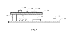
図1は、第1の回路基板102を第2の回路基板104に電気的に接続するためのインターフェースコネクタ100のある実施形態を示す。インターフェースコネクタ100は、第1の基板102上の電子部品106に関連する電子回路が、第2の基板上の電子部品108に関連する電子回路と接続するための、ブリッジを提供する。回路基板102、104は、当業者に知られているような回路基板であり、抵抗、コンデンサ、プロセッサ、フィールドプログラマブルゲートアレイ(FPGA)など電子部品106、108が導電性の経路を通じて取り付けられ相互接続される、非導電性の基部を一般に含む。一般にある態様では、インターフェースコネクタは、ケーシングと、ケーシング内で互いに絶縁されている複数の導電性コネクタを含む。ある態様では、インターフェースコネクタ100の実施形態は、ニューヨーク州スケネクタディのGeneral Electric社(GE)で製造されるような機械監視システムにおいて使用されうる。ある態様では、インターフェースコネクタの実施形態は、機械監視システムで使用される監視モジュールをグレードアップするために使用されうる。そのような機械監視システムおよびグレードアップ用監視モジュールは、2010年9月20日に出願された米国特許出願第12/885992号で説明されており、上記の出願は参照によって全体が本明細書に組み込まれ、本明細書の一部となる。ある態様では、第1の回路基板102は、Bently−Nevada機械保護および監視システム用の補助基板である(Bently NevadaはGeneral Electric社の商標である)。ある態様では、第2の回路基板104は、Bently Nevadaモデル3300機械保護および監視システムをBently Nevadaモデル3500機械保護および監視システムにグレードアップするために使用される移植可能なコアモジュール(PCM)である。ある態様では、PCMは、多くのプラットフォームに容易に移植可能でありうる、コア監視および保護機能を実行するマイクロプロセッサベースのモジュールである。ある態様では、インターフェースコネクタ100は、Bently Nevada機械保護および監視システムのための、補助基板と移植可能なコアモジュールとの間の移植可能なコアモジュールのインターフェースコネクタとしての役割を果たす。しかし、別の使用法および応用が、本発明の実施形態の範囲内にあると考えられる。
FIG. 1 illustrates one embodiment of an
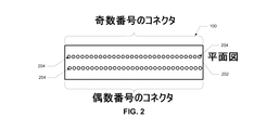
図2は、第1の回路基板102を第2の回路基板104に電気的に接続するためのインターフェースコネクタ100のある実施形態の平面図を示す。図2に示されるように、インターフェースコネクタ100のこの実施形態は、ケーシング202と、ケーシング202内で互いに絶縁されている複数の導電性コネクタ204とを含み、各コネクタ204は第1の端部および第2の端部を有する。ある態様では、コネクタ204の第1の端部は第1の回路基板102に接続し、コネクタ204の第2の端部は第2の回路基板104に接続する。図2に説明されるように、複数のコネクタ204は、第1の列および第2の列を形成する。ある態様では、第1の列は偶数番号のコネクタ204を含み、第2の列は奇数番号のコネクタを含む。例えば、偶数番号のコネクタは、2、4、6、8、10などであってよい。奇数番号のコネクタ204は、1、3、5、7、9、11などであってよい。
FIG. 2 shows a top view of an embodiment of an
図3は、第1の回路基板102を第2の回路基板104に電気的に接続するためのインターフェースコネクタ100のある実施形態の立体図を示す。図3に示すように、コネクタ204はケーシング202を通って延び、それぞれが導電性の経路を形成して、第1の回路基板102上の回路を第2の回路基板104の回路と接続する。上述のように、各コネクタ204は、第1の端部302および第2の端部304を有する。コネクタ204の第1の端部302および第2の端部304は、回路基板102、104とインターフェースするために必要とされるので、オス型またはメス型であってよい。ある態様では、複数のコネクタ204の各々の第1の端部302は、第1の回路基板102に接続するためのメス型端部を含む。別の態様では、複数のコネクタ204の各々の第1の端部302は、第1の回路基板102に接続するためのオス型端部を含む。ある態様では、複数のコネクタ204の各々の第2の端部304は、第2の回路基板104に接続するためのメス型端部を含む。別の態様では、複数のコネクタ204の各々の第2の端部304は、第2の回路基板104に接続するためのオス型端部を含む。別の種類のコネクタ端部も、本発明の実施形態の範囲内であると考えられる。
FIG. 3 illustrates a three-dimensional view of an embodiment of an
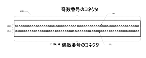
図4は、2列のコネクタ402を含むインターフェースコネクタ400のある実施形態を示す。コネクタ402は、インターフェースコネクタ400の1つの列404の全てのコネクタ402が偶数番号となり、別の列406の全てのコネクタ402が全て奇数番号となるように、番号付けされる。
FIG. 4 illustrates an embodiment of an
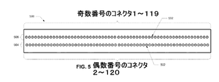
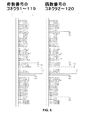
図5は、120個のコネクタ502を含むインターフェースコネクタ500のある実施形態を示す。コネクタ502は、各列504、506内に60個のコネクタ502を有する2つの列504、506に分けられる。コネクタ502は、インターフェースコネクタ500の1つの列504内の全てのコネクタ502が偶数番号となり(2〜120の番号を付けられる)、別の列506内の全てのコネクタ502が全て奇数の番号となる(1〜119の番号を付けられる)ように、番号を付けられる。図6は、インターフェースコネクタのピン配置のある実施形態の図である。このピン配置の図は、機械保護および監視システムの補助基板を第2の回路基板に接続するためのものである。この実施形態では、第2の回路基板は、機械保護および監視システムをグレードアップするのに使用される、移植可能なコアモジュール(PCM)である。特に、図6のピン配置の図は、Bently Nevadaモデル3300機械保護および監視システムの補助基板を、モデル3300シリーズからモデル3500シリーズの機械保護および監視システムにグレードアップできるPCMに、接続するためのものである。図6に示されるように、少なくともコネクタ(本明細書では「ピン」とも呼ばれる)1〜4、13〜18、43〜61、68〜71、77、78、79、80、84、86、92および94〜120は、第1の回路基板と第2の回路基板との間の一般的な回路接続のための電気的な経路を提供し、コネクタ41、42、62〜67、72〜75および81は、第1の回路基板と第2の回路基板との間のホストプロセッサの接続のための電気的な経路を提供し、コネクタ5〜12、19〜40、76、82、83、85、87〜91および93は、第1の回路基板と第2の回路基板との間のフィールドプログラマブルゲートアレイ(FPGA)の接続のための電気的な経路を提供する。より具体的には、コネクタ59、61、79、18、60、80、110、69、71、68、70、77および78は、第1の回路基板または第2の回路基板の上の電子部品のための電源の接続である。ある態様では、第1の回路基板または第2の回路基板の上の電子部品は、ホストプロセッサおよびFPGAを含む。コネクタ1〜4は、第1の回路基板と第2の回路基板との間の複数のkeyphasor(General Electric社の登録商標)信号のための電気的な経路を提供する。keyphasor(登録商標)信号は、機械監視および診断に使用される。この信号は、回転軸のある点から得られる、電子的パルス、またはトリガである。この信号は、回転子および機械に関係する別の測定値の、位相0の参照値としての役割を果たす。コネクタ63は、第1の回路基板と第2の回路基板との間のクロック信号のための、電気的な経路を提供する。
FIG. 5 illustrates an embodiment of an
以下の表1は、具体的に、Bently Nevada補助基板を、一般的な回路接続、ホストプロセッサの接続、およびFPGAの接続を含むBently Nevada PCMに接続するのに使用される、インターフェースコネクタの完全な接続情報を与える。 Table 1 below shows the complete interface connector used to specifically connect the Bently Nevada auxiliary board to the Bently Nevada PCM, including general circuit connections, host processor connections, and FPGA connections. Give connection information.

図7は、2つの回路基板を接続する方法のある実施形態を示すフローチャートである。ステップ702において、インターフェースコネクタは以下のように構成される。コネクタ1〜4、13〜18、43〜61、68〜71、77、78、79、80、84、86、92および94〜120は、第1の回路基板と第2の回路基板との間の一般的な回路接続のための電気的な経路を提供するように割り当てられ、コネクタ41、42、62〜67、72〜75、および81は、第1の回路基板と第2の回路基板との間のホストプロセッサの接続のための電気的な経路を提供するように割り当てられ、コネクタ5〜12、19〜40、76、82、83、85、87〜91、および93は、第1の回路基板と第2の回路基板との間のフィールドプログラマブルゲートアレイ(FPGA)の接続のための電気的な経路を提供するように割り当てられる。インターフェースコネクタは、ケーシングと、ケーシング内で互いに絶縁されている複数の導電性コネクタとを含み、各コネクタは第1の端部および第2の端部を有する。第1の端部は第1の回路基板に接続し、第2の端部は第2の回路基板に接続する。複数のコネクタは第1の列および第2の列を形成し、第1の列は偶数番号のコネクタを含み、前記第2の列は奇数番号のコネクタで形成される。ある態様では、複数の導電性コネクタは、少なくとも120個のコネクタを含む。ある態様では、コネクタ1〜4、13〜18、43〜61、68〜71、77、78、79、80、84、86、92および94〜120が、第1の回路基板と第2の回路基板との間の一般的な回路接続のための電気的な経路を提供するように、インターフェースコネクタを構成するステップは、コネクタ59、61、79、18、60、80、110、69、71、68、70、77および78を、第1の回路基板または第2の回路基板の上の電子部品のための電源の接続として構成するステップを含む。ある態様では、第1の回路基板または第2の回路基板の上の電子部品は、ホストプロセッサおよびFPGAを含む。ある態様では、コネクタ1〜4、13〜18、43〜61、68〜71、77、78、79、80、84、86、92および94〜120が、第1の回路基板と第2の回路基板との間の一般的な回路接続のための電気的な経路を提供するように、インターフェースコネクタを構成するステップは、第1の回路基板と第2の回路基板との間の複数のkeyphasor(登録商標)信号のための電気的な経路を提供するように、コネクタ1〜4を構成するステップを含む。ある態様では、コネクタ41、42、62〜67、72〜75、および81が、第1の回路基板と第2の回路基板との間のホストプロセッサの接続のための電気的な経路を提供するように、インターフェースコネクタを構成するステップは、第1の回路基板と第2の回路基板との間でクロック信号のための電気的な経路を提供するようにコネクタ63を構成することを含む。ステップ704において、構成されたインターフェースコネクタは、第1の回路基板および第2の回路基板を接続するのに使用される。
FIG. 7 is a flowchart illustrating an embodiment of a method for connecting two circuit boards. In
上述のように、かつ当業者には理解されるように、本発明の実施形態は、デバイス、システム、または方法として構成されうる。別段明示的に述べられない限り、本明細書で述べられたあらゆる方法は、そのステップがある特定の順序で実行されなければならないと解釈されることは決して意図されていない。したがって、方法の請求項が、方法のステップが従うべき順序を実際に記載しない場合、または、請求項または説明においてステップが特定の順序に限定されるべきであると別段具体的に述べられていない場合、あらゆる面において、ある順序が暗示されることは決して意図されていない。これは、ステップまたは動作の流れの構成に関する論理的な事項、文法的な構造または句読点から導かれる単純な意味、本明細書で説明される実施形態の数または種類を含む、解釈に関して可能性のあるあらゆる非明示的な原則に対して当てはまる。 As described above and as will be appreciated by one skilled in the art, embodiments of the present invention may be configured as a device, system, or method. Unless explicitly stated otherwise, any method described herein is not intended to be construed in any way as its steps must be performed in a certain order. Accordingly, the claims of a method do not specifically state that the order in which the steps of the method should follow is not actually stated, or that the steps in the claim or description should be limited to a particular order In all cases, in some respects, an order is never intended to be implied. This may be possible with respect to interpretation, including logical matters relating to the organization of steps or operational flows, simple meanings derived from grammatical structures or punctuation marks, and the number or type of embodiments described herein. This is true for any implicit principle.
本出願全体を通じて、様々な刊行物が参照されることがある。これらの刊行物の開示の全体が、デバイス、方法およびシステムに関係する最新技術をより完全に説明するために、本明細書で参照によって本出願に組み込まれる。 Throughout this application various publications may be referenced. The entire disclosures of these publications are hereby incorporated by reference into the present application to more fully describe the state of the art relating to devices, methods and systems.
前述の説明および関連する図面に示される教示の利益を有し本発明のこれらの実施形態に関係する当業者には、本明細書で述べられた本発明の多くの修正および別の実施形態が想起されるであろう。したがって、本発明の実施形態は開示された特定の実施形態に限定されるべきではなく、修正および別の実施形態が添付の特許請求の範囲に含まれることが意図されることを、理解されたい。さらに、前述の説明および関連する図面は、要素および/または機能のある例示的な組合せに関する例示的な実施形態を説明するが、要素および/または機能の異なる組合せが、添付の特許請求の範囲から逸脱することなく、代替的な実施形態によって提供されうることを、理解されたい。この点において、例えば、上で明示的に説明された要素および/または機能の組合せとは異なる組合せも、添付の特許請求の範囲の一部で述べられることがある。特定の用語が本明細書で使用されたが、それらの用語は、限定するためではなく包括的かつ説明的な意味でのみ用いられる。 Many modifications and alternative embodiments of the invention described herein will occur to those skilled in the art having the benefit of the teachings presented in the foregoing description and the associated drawings and relating to these embodiments of the invention. It will be recalled. Accordingly, it is to be understood that embodiments of the invention should not be limited to the particular embodiments disclosed, but that modifications and alternative embodiments are intended to be included within the scope of the appended claims. . Moreover, while the foregoing description and associated drawings describe exemplary embodiments relating to certain exemplary combinations of elements and / or functions, different combinations of elements and / or functions are contemplated by the appended claims. It should be understood that alternative embodiments may be provided without departing. In this respect, for example, combinations different from the combinations of elements and / or functions explicitly described above may also be set forth in part of the appended claims. Although specific terms are used herein, the terms are used in a comprehensive and descriptive sense only, not for purposes of limitation.
100 インターフェースコネクタ
102 第1の回路基板
104 第2の回路基板
106 第1の回路基板102上の電子部品
108 第2の回路基板上の電子部品108
202 ケーシング
204 複数の導電性コネクタ
302 (導電性コネクタ204の)第1の端部
304 (導電性コネクタ204の)第2の端部
400 インターフェースコネクタ
402 コネクタ
404 インターフェースコネクタの1つの列(偶数番号)
406 インターフェースコネクタの別の列(奇数番号)
500 インターフェースコネクタ
502 コネクタ
504 インターフェースコネクタ500の1つの列504内のコネクタ502は偶数番号である(2〜120の番号を付けられる)
506 別の列506のコネクタ502は全て奇数番号である(1〜119の番号を付けられる)
DESCRIPTION OF
202
406 Another row of interface connectors (odd number)
500
506 The
Claims (10)
ケーシング(202)と、
前記ケーシング(202)内で互いに絶縁され、各コネクタ(204)が第1の端部(302)および第2の端部(304)を有する導電性コネクタ(204)とを含み、前記第1の端部(302)が第1の回路基板(102)に接続し、前記第2の端部(304)が第2の回路基板(104)に接続し、前記複数のコネクタ(204)が第1の列(404)および第2の列(406)を形成し、前期第1の列(404)が偶数番号のコネクタ(204)を含み、前記第2の列(406)が奇数番号のコネクタ(204)を含み、前記複数のコネクタ(204)が、
コネクタ1〜4、13〜18、43〜61、68〜71、77、78、79、80、84、86、92および94〜120が、前記第1の回路基板(102)と前記第2の回路基板(104)との間の一般的な回路の接続のための電気的な経路を提供し、
コネクタ41、42、62〜67、72〜75および81が、前記第1の回路基板(102)と前記第2の回路基板(104)との間のホストプロセッサの接続のための電気的な経路を提供し、
コネクタ5〜12、19〜40、76、82、83、85、87〜91および93が、前記第1の回路基板(102)と前記第2の回路基板(104)との間のフィールドプログラマブルゲートアレイ(FPGA)の接続のための電気的な経路を提供する
ように割り当てられる、インターフェースコネクタ。 An interface connector for connecting two circuit boards,
A casing (202);
A conductive connector (204) insulated from each other in the casing (202), each connector (204) having a first end (302) and a second end (304); The end (302) is connected to the first circuit board (102), the second end (304) is connected to the second circuit board (104), and the plurality of connectors (204) are the first. Column (404) and second column (406), the first column (404) includes an even numbered connector (204), and the second column (406) is an odd numbered connector ( 204), and the plurality of connectors (204)
Connectors 1-4, 13-18, 43-61, 68-71, 77, 78, 79, 80, 84, 86, 92 and 94-120 are connected to the first circuit board (102) and the second Providing an electrical path for general circuit connections to and from the circuit board (104);
Connectors 41, 42, 62-67, 72-75 and 81 are electrical paths for host processor connection between the first circuit board (102) and the second circuit board (104). Provide
Connectors 5-12, 19-40, 76, 82, 83, 85, 87-91 and 93 are field programmable gates between the first circuit board (102) and the second circuit board (104). An interface connector assigned to provide an electrical path for array (FPGA) connections.
コネクタ1〜4が、前記第1の回路基板(102)と前記第2の回路基板(104)との間の複数のkeyphasor(登録商標)信号のための電気的な経路を提供し、
コネクタ63が、前記第1の回路基板(102)と前記第2の回路基板(104)との間のクロック信号のための電気的な経路を提供し、
コネクタ48および56が、前記第1の回路基板(102)と前記第2の回路基板(104)との間のトリップ乗算信号のための電気的な経路を提供し、
コネクタ24〜39が、前記第1の回路基板(102)と前記第2の回路基板(104)との間の管理データバス信号のための電気的な経路を提供する、請求項1記載のインターフェースコネクタ。 Connectors 59, 61, 79, 18, 60, 80, 110, 69, 71, 68, 70, 77, and 78 are on the first circuit board (102) or the second circuit board (104). Power supply connection for electronic components,
Connectors 1-4 provide an electrical path for a plurality of keyphasor signals between the first circuit board (102) and the second circuit board (104);
A connector 63 provides an electrical path for a clock signal between the first circuit board (102) and the second circuit board (104);
Connectors 48 and 56 provide an electrical path for trip multiplication signals between the first circuit board (102) and the second circuit board (104);
The interface of claim 1, wherein connectors 24-39 provide an electrical path for management data bus signals between the first circuit board (102) and the second circuit board (104). connector.
インターフェースコネクタ(100)を設けるステップであって、前記インターフェースコネクタ(100)が、ケーシング(202)と、前記ケーシング(202)内で互いに絶縁され、各コネクタ(204)が第1の端部(302)および第2の端部(304)を有する導電性コネクタ(204)とを含み、前記第1の端部(302)が第1の回路基板(102)に接続し、前記第2の端部(304)が第2の回路基板(104)に接続し、前記複数のコネクタ(204)が第1の列(404)および第2の列(406)を形成し、前期第1の列(404)が偶数番号のコネクタ(204)を含み、前記第2の列(406)が奇数番号のコネクタ(204)を含み、前記複数の導電性コネクタ(204)が、少なくとも120個のコネクタを含む、ステップと、
前記複数のコネクタ(204)が、
コネクタ1〜4、13〜18、43〜61、68〜71、77、78、79、80、84、86、92および94〜120が、前記第1の回路基板(102)と前記第2の回路基板(104)との間の一般的な回路の接続のための電気的な経路を提供し、
コネクタ41、42、62〜67、72〜75および81が、前記第1の回路基板(102)と前記第2の回路基板(104)との間のホストプロセッサの接続のための電気的な経路を提供し、
コネクタ5〜12、19〜40、76、82、83、85、87〜91および93が、前記第1の回路基板(102)と前記第2の回路基板(104)との間のフィールドプログラマブルゲートアレイ(FPGA)の接続のための電気的な経路を提供する
ように割り当てられるように、前記インターフェースコネクタ(100)を構成するステップと、
前記構成されたインターフェースコネクタ(100)を用いて、前記第1の回路基板(102)および前記第2の回路基板(104)を接続するステップと
を含む、方法。 A method for connecting two circuit boards, comprising:
Providing an interface connector (100), the interface connector (100) being insulated from each other in the casing (202) and the casing (202), each connector (204) being a first end (302); ) And a conductive connector (204) having a second end (304), wherein the first end (302) connects to a first circuit board (102), and the second end (304) connects to the second circuit board (104), and the plurality of connectors (204) form a first row (404) and a second row (406), and the first row (404) ) Includes even numbered connectors (204), the second row (406) includes odd numbered connectors (204), and the plurality of conductive connectors (204) includes at least 120 connectors. Including the steps,
The plurality of connectors (204),
Connectors 1-4, 13-18, 43-61, 68-71, 77, 78, 79, 80, 84, 86, 92 and 94-120 are connected to the first circuit board (102) and the second Providing an electrical path for general circuit connections to and from the circuit board (104);
Connectors 41, 42, 62-67, 72-75 and 81 are electrical paths for host processor connection between the first circuit board (102) and the second circuit board (104). Provide
Connectors 5-12, 19-40, 76, 82, 83, 85, 87-91 and 93 are field programmable gates between the first circuit board (102) and the second circuit board (104). Configuring the interface connector (100) to be assigned to provide an electrical path for connection of an array (FPGA);
Connecting the first circuit board (102) and the second circuit board (104) using the configured interface connector (100).
前記第1の回路基板(102)または前記第2の回路基板(104)の上の電子部品が、ホストプロセッサおよびFPGAを含み、
コネクタ41、42、62〜67、72〜75および81が、前記第1の回路基板と前記第2の回路基板との間のホストプロセッサの接続のための電気的な経路を提供するように、前記インターフェースコネクタを構成するステップが、前記第1の回路基板と前記第2の回路基板との間のクロック信号のための電気的な経路を提供するようにコネクタ63を構成するステップを含み、
コネクタ5〜12、19〜40、76、82、83、85、87〜91および93が、前記第1の回路基板と前記第2の回路基板との間のフィールドプログラマブルゲートアレイ(FPGA)の接続のための電気的な経路を提供するように、前記インターフェースコネクタを構成するステップが、前記第1の回路基板と前記第2の回路基板との間の管理データバス信号のための電気的な経路として、コネクタ24〜39を構成するステップを含む、請求項6記載の方法。 Connectors 1-4, 13-18, 43-61, 68-71, 77, 78, 79, 80, 84, 86, 92 and 94-120 are connected to the first circuit board (102) and the second Configuring the interface connector (100) to provide an electrical path for general circuit connection to and from the circuit board (104) includes connectors 59, 61, 79, 18, 60 , 80, 110, 69, 71, 68, 70, 77 and 78 as power connections for electronic components on the first circuit board (102) or the second circuit board (104) And configuring connectors 1-4 to provide an electrical path for a plurality of keyphasor signals between the first circuit board and the second circuit board. , As an electrical pathway for trip multiplied signal between the first circuit board and the second circuit board, and a step of constructing a connector 48 and 56,
The electronic components on the first circuit board (102) or the second circuit board (104) include a host processor and an FPGA,
Connectors 41, 42, 62-67, 72-75 and 81 provide an electrical path for a host processor connection between the first circuit board and the second circuit board; Configuring the interface connector includes configuring the connector 63 to provide an electrical path for a clock signal between the first circuit board and the second circuit board;
Connectors 5-12, 19-40, 76, 82, 83, 85, 87-91 and 93 are field programmable gate array (FPGA) connections between the first circuit board and the second circuit board. Configuring the interface connector to provide an electrical path for a management data bus signal between the first circuit board and the second circuit board. The method of claim 6 including the step of configuring the connectors 24-39.
第1の回路基板(102)と、
第2の回路基板(104)と
を含むシステムであって、前記インターフェースコネクタ(100)が、前記第1の回路基板(102)を前記第2の回路基板(104)に接続するのに使用され、前記インターフェースコネクタ(100)が、
ケーシング(202)と、
前記ケーシング(202)内で互いに絶縁され、各コネクタ(204)が第1の端部(302)および第2の端部(304)を有する少なくとも120個の導電性コネクタ(204)とを含み、前記第1の端部(302)が前記第1の回路基板(102)に接続し、前記第2の端部(304)が前記第2の回路基板(104)に接続し、前記複数のコネクタ(204)が第1の列(404)および第2の列(406)を形成し、前期第1の列(404)が偶数番号のコネクタ(204)を含み、前記第2の列(406)が奇数番号のコネクタ(204)を含み、前記複数のコネクタ(204)が、
コネクタ1〜4、13〜18、43〜61、68〜71、77、78、79、80、84、86、92および94〜120が、前記第1の回路基板(102)と前記第2の回路基板(104)との間の一般的な回路の接続のための電気的な経路を提供し、コネクタ59、61、79、18、60、80、110、69、71、68、70、77および78が、前記第1の回路基板(102)または前記第2の回路基板(104)の上の電子部品のための電源の接続であり、コネクタ1〜4が、前記第1の回路基板(102)と前記第2の回路基板(104)との間の複数のkeyphasor(登録商標)信号のための電気的な経路を提供し、コネクタ48および56が、前記第1の回路基板(102)と前記第2の回路基板(104)との間のトリップ乗算信号のための電気的な経路を提供し、
コネクタ41、42、62〜67、72〜75および81が、前記第1の回路基板(102)と前記第2の回路基板(104)との間のホストプロセッサの接続のための電気的な経路を提供し、コネクタ63が、前記第1の回路基板(102)と前記第2の回路基板(104)との間のクロック信号のための電気的な経路を提供し、
コネクタ5〜12、19〜40、76、82、83、85、87〜91および93が、前記第1の回路基板(102)と前記第2の回路基板(104)との間のフィールドプログラマブルゲートアレイ(FPGA)の接続のための電気的な経路を提供し、コネクタ24〜39が、前記第1の回路基板(102)と前記第2の回路基板(104)との間の管理データバス信号のための電気的な経路を提供する
ように構成される、システム。 An interface connector (100);
A first circuit board (102);
A second circuit board (104), wherein the interface connector (100) is used to connect the first circuit board (102) to the second circuit board (104). The interface connector (100) is
A casing (202);
At least 120 conductive connectors (204) insulated from each other within the casing (202), each connector (204) having a first end (302) and a second end (304); The first end (302) is connected to the first circuit board (102), the second end (304) is connected to the second circuit board (104), and the plurality of connectors (204) forms a first column (404) and a second column (406), the first column (404) includes an even numbered connector (204), said second column (406) Includes odd numbered connectors (204), wherein the plurality of connectors (204) include:
Connectors 1-4, 13-18, 43-61, 68-71, 77, 78, 79, 80, 84, 86, 92 and 94-120 are connected to the first circuit board (102) and the second Provides an electrical path for general circuit connection to and from the circuit board (104), and connectors 59, 61, 79, 18, 60, 80, 110, 69, 71, 68, 70, 77 And 78 are power connections for electronic components on the first circuit board (102) or the second circuit board (104), and connectors 1 to 4 are connected to the first circuit board (102). 102) and the second circuit board (104) provide an electrical path for a plurality of keyphasor signals, and connectors 48 and 56 are provided on the first circuit board (102). And the second circuit board (104) Providing an electrical pathway for the trip multiplication signal,
Connectors 41, 42, 62-67, 72-75 and 81 are electrical paths for host processor connection between the first circuit board (102) and the second circuit board (104). A connector 63 provides an electrical path for a clock signal between the first circuit board (102) and the second circuit board (104);
Connectors 5-12, 19-40, 76, 82, 83, 85, 87-91 and 93 are field programmable gates between the first circuit board (102) and the second circuit board (104). Provide an electrical path for array (FPGA) connections, and connectors 24-39 are management data bus signals between the first circuit board (102) and the second circuit board (104) A system that is configured to provide an electrical path for.
Applications Claiming Priority (2)
| Application Number | Priority Date | Filing Date | Title |
|---|---|---|---|
| US13/022,808 | 2011-02-08 | ||
| US13/022,808 US8287290B2 (en) | 2011-02-08 | 2011-02-08 | Device, system and method of an interface connector |
Publications (2)
| Publication Number | Publication Date |
|---|---|
| JP2012164313A true JP2012164313A (en) | 2012-08-30 |
| JP2012164313A5 JP2012164313A5 (en) | 2012-11-22 |
Family
ID=46547172
Family Applications (1)
| Application Number | Title | Priority Date | Filing Date |
|---|---|---|---|
| JP2012023564A Pending JP2012164313A (en) | 2011-02-08 | 2012-02-07 | Device, system and method of interface connector |
Country Status (6)
| Country | Link |
|---|---|
| US (1) | US8287290B2 (en) |
| JP (1) | JP2012164313A (en) |
| CN (1) | CN102683930A (en) |
| DE (1) | DE102012100954A1 (en) |
| DK (1) | DK177849B1 (en) |
| IN (1) | IN2012DE00268A (en) |
Families Citing this family (4)
| Publication number | Priority date | Publication date | Assignee | Title |
|---|---|---|---|---|
| CN104347973B (en) | 2013-08-01 | 2016-09-28 | 富士康(昆山)电脑接插件有限公司 | Connector assembly |
| US10001459B2 (en) | 2015-02-27 | 2018-06-19 | General Electric Company | System and method for phased array edge card |
| US10028402B1 (en) * | 2017-03-22 | 2018-07-17 | Seagate Technology Llc | Planar expansion card assembly |
| TWI721791B (en) * | 2020-02-21 | 2021-03-11 | 緯穎科技服務股份有限公司 | Electronic device |
Citations (10)
| Publication number | Priority date | Publication date | Assignee | Title |
|---|---|---|---|---|
| JPS5621389U (en) * | 1979-07-27 | 1981-02-25 | ||
| JPH0221305A (en) * | 1988-07-08 | 1990-01-24 | Omron Tateisi Electron Co | Electronic equipment for control |
| JPH0324279U (en) * | 1989-07-18 | 1991-03-13 | ||
| JPH0566707U (en) * | 1992-02-17 | 1993-09-03 | 株式会社キーエンス | I / O controller |
| JPH06349554A (en) * | 1993-06-02 | 1994-12-22 | Japan Aviation Electron Ind Ltd | Connector for parallel board, and board |
| JPH09146625A (en) * | 1995-11-24 | 1997-06-06 | Advantest Corp | Timing adjusting device corresponding to adjusting board |
| JPH09179606A (en) * | 1995-12-22 | 1997-07-11 | Toei Denki Kk | Servo controller |
| JP2002135218A (en) * | 2000-10-25 | 2002-05-10 | Kawamura Electric Inc | Network environment monitor |
| JP2002533047A (en) * | 1998-12-17 | 2002-10-02 | エス・ピー・ディ、テクノロジーズ、インコーポレーテッド | Power node control center |
| JP2005512219A (en) * | 2001-12-06 | 2005-04-28 | フィッシャー−ローズマウント システムズ, インコーポレイテッド | Field maintenance tools with inherent safety |
Family Cites Families (15)
| Publication number | Priority date | Publication date | Assignee | Title |
|---|---|---|---|---|
| US5313614A (en) | 1988-12-06 | 1994-05-17 | At&T Bell Laboratories | Method and apparatus for direct conversion of programs in object code form between different hardware architecture computer systems |
| US5539787A (en) | 1992-07-06 | 1996-07-23 | Sharp Kabushiki Kaisha | Converter for connecting modem equipment of dissimilar interface protocol |
| JP3670303B2 (en) | 1993-09-01 | 2005-07-13 | 富士通株式会社 | Data conversion method and data conversion apparatus |
| US5732273A (en) | 1995-08-11 | 1998-03-24 | Digital Equipment Corporation | System for monitoring compute system performance |
| US5581558A (en) | 1995-03-29 | 1996-12-03 | Lucent Technologies Inc. | Apparatus for bridging non-compatible network architectures |
| JP3904645B2 (en) | 1996-12-26 | 2007-04-11 | 株式会社東芝 | Hardware / software co-simulation equipment |
| US6151390A (en) | 1997-07-31 | 2000-11-21 | Cisco Technology, Inc. | Protocol conversion using channel associated signaling |
| US6237053B1 (en) | 1998-06-30 | 2001-05-22 | Symbol Technologies, Inc. | Configurable operating system having multiple data conversion applications for I/O connectivity |
| US6493594B1 (en) | 1999-06-04 | 2002-12-10 | Lucent Technologies Inc. | System and method for improved software configuration and control management in multi-module systems |
| US7188171B2 (en) | 2003-01-23 | 2007-03-06 | Hewlett-Packard Development Company, L.P. | Method and apparatus for software and hardware event monitoring and repair |
| TWI282645B (en) * | 2004-04-16 | 2007-06-11 | Hon Hai Prec Ind Co Ltd | Electrical contact |
| CN200941464Y (en) * | 2006-06-23 | 2007-08-29 | 富士康(昆山)电脑接插件有限公司 | Electrical connector |
| US7341485B2 (en) * | 2006-07-24 | 2008-03-11 | Hon Hai Precision Ind. Co., Ltd. | Land grid array socket |
| US7692281B2 (en) * | 2007-02-16 | 2010-04-06 | Tyco Electronics Corporation | Land grid array module with contact locating features |
| TWM351483U (en) * | 2008-08-04 | 2009-02-21 | Hon Hai Prec Ind Co Ltd | Electrical connector |
-
2011
- 2011-02-08 US US13/022,808 patent/US8287290B2/en active Active
-
2012
- 2012-01-31 IN IN268DE2012 patent/IN2012DE00268A/en unknown
- 2012-02-03 DK DK201270054A patent/DK177849B1/en active
- 2012-02-06 DE DE102012100954A patent/DE102012100954A1/en active Pending
- 2012-02-07 JP JP2012023564A patent/JP2012164313A/en active Pending
- 2012-02-08 CN CN2012100346532A patent/CN102683930A/en active Pending
Patent Citations (10)
| Publication number | Priority date | Publication date | Assignee | Title |
|---|---|---|---|---|
| JPS5621389U (en) * | 1979-07-27 | 1981-02-25 | ||
| JPH0221305A (en) * | 1988-07-08 | 1990-01-24 | Omron Tateisi Electron Co | Electronic equipment for control |
| JPH0324279U (en) * | 1989-07-18 | 1991-03-13 | ||
| JPH0566707U (en) * | 1992-02-17 | 1993-09-03 | 株式会社キーエンス | I / O controller |
| JPH06349554A (en) * | 1993-06-02 | 1994-12-22 | Japan Aviation Electron Ind Ltd | Connector for parallel board, and board |
| JPH09146625A (en) * | 1995-11-24 | 1997-06-06 | Advantest Corp | Timing adjusting device corresponding to adjusting board |
| JPH09179606A (en) * | 1995-12-22 | 1997-07-11 | Toei Denki Kk | Servo controller |
| JP2002533047A (en) * | 1998-12-17 | 2002-10-02 | エス・ピー・ディ、テクノロジーズ、インコーポレーテッド | Power node control center |
| JP2002135218A (en) * | 2000-10-25 | 2002-05-10 | Kawamura Electric Inc | Network environment monitor |
| JP2005512219A (en) * | 2001-12-06 | 2005-04-28 | フィッシャー−ローズマウント システムズ, インコーポレイテッド | Field maintenance tools with inherent safety |
Also Published As
| Publication number | Publication date |
|---|---|
| DE102012100954A1 (en) | 2012-08-09 |
| US20120202362A1 (en) | 2012-08-09 |
| CN102683930A (en) | 2012-09-19 |
| DK177849B1 (en) | 2014-09-22 |
| DK201270054A (en) | 2012-08-09 |
| IN2012DE00268A (en) | 2015-07-10 |
| US8287290B2 (en) | 2012-10-16 |
Similar Documents
| Publication | Publication Date | Title |
|---|---|---|
| TWI618380B (en) | Management methods, service controller devices and non-stransitory, computer-readable media | |
| CN107444481A (en) | Rotary sensing device and use its electric power steering apparatus | |
| JP2012164313A (en) | Device, system and method of interface connector | |
| US20040158627A1 (en) | Computer condition detection system | |
| CN109522175B (en) | Memory evaluation method and device | |
| CN103250107A (en) | Intelligent detecting system and detecting method for detecting fault of device | |
| US20150058482A1 (en) | System insight display | |
| JP5441875B2 (en) | Computer system | |
| CN108955951A (en) | A kind of temperature sensor fault judgment method and device | |
| EP2787630B1 (en) | Detecting faults in motors and drives | |
| JP6033913B2 (en) | Universal test platform and test method thereof | |
| JP6069406B2 (en) | Heat dissipation system, control method, computer program, and information processing apparatus | |
| CN112015689A (en) | Serial port output path switching method, system and device and switch | |
| TW201418967A (en) | Electronic apparatus and management method thereof and rack server system | |
| EP3068052A1 (en) | Industrial control system with integrated circuit elements partitioned for functional safety and employing watchdog timing circuits | |
| CN113656339A (en) | NVME hot plug processing method, BMC, device, equipment and medium | |
| CN106446311B (en) | CPU warning circuit and alarm method | |
| CN110083532B (en) | Method and device for positioning operation errors in fusion mode based on deep learning framework | |
| JP2012164313A5 (en) | ||
| CN103620558A (en) | A method for achieving correspondence of physical resource and virtual resource and a basic input output system | |
| US20150365269A1 (en) | Usage of mapping jumper pins or dip switch setting to define node's ip address to identify node's location | |
| TWI718807B (en) | Server with vibration sensing function | |
| KR101028885B1 (en) | Instrumentation system for measuring and control | |
| TW201740288A (en) | Method and system of flexible server configuration | |
| CN102478861B (en) | Fan control system for memory |
Legal Events
| Date | Code | Title | Description |
|---|---|---|---|
| A521 | Written amendment |
Free format text: JAPANESE INTERMEDIATE CODE: A523 Effective date: 20121009 |
|
| A621 | Written request for application examination |
Free format text: JAPANESE INTERMEDIATE CODE: A621 Effective date: 20121009 |
|
| A871 | Explanation of circumstances concerning accelerated examination |
Free format text: JAPANESE INTERMEDIATE CODE: A871 Effective date: 20121009 |
|
| A975 | Report on accelerated examination |
Free format text: JAPANESE INTERMEDIATE CODE: A971005 Effective date: 20121030 |
|
| A131 | Notification of reasons for refusal |
Free format text: JAPANESE INTERMEDIATE CODE: A131 Effective date: 20121106 |
|
| A521 | Written amendment |
Free format text: JAPANESE INTERMEDIATE CODE: A523 Effective date: 20130131 |
|
| A02 | Decision of refusal |
Free format text: JAPANESE INTERMEDIATE CODE: A02 Effective date: 20130402 |