JP2012145910A - Structure - Google Patents
Structure Download PDFInfo
- Publication number
- JP2012145910A JP2012145910A JP2011218414A JP2011218414A JP2012145910A JP 2012145910 A JP2012145910 A JP 2012145910A JP 2011218414 A JP2011218414 A JP 2011218414A JP 2011218414 A JP2011218414 A JP 2011218414A JP 2012145910 A JP2012145910 A JP 2012145910A
- Authority
- JP
- Japan
- Prior art keywords
- structure according
- component
- adhesive
- fixed
- bonded
- Prior art date
- Legal status (The legal status is an assumption and is not a legal conclusion. Google has not performed a legal analysis and makes no representation as to the accuracy of the status listed.)
- Ceased
Links
Images


Classifications
-
- G—PHYSICS
- G02—OPTICS
- G02B—OPTICAL ELEMENTS, SYSTEMS OR APPARATUS
- G02B26/00—Optical devices or arrangements for the control of light using movable or deformable optical elements
- G02B26/08—Optical devices or arrangements for the control of light using movable or deformable optical elements for controlling the direction of light
- G02B26/0816—Optical devices or arrangements for the control of light using movable or deformable optical elements for controlling the direction of light by means of one or more reflecting elements
- G02B26/0833—Optical devices or arrangements for the control of light using movable or deformable optical elements for controlling the direction of light by means of one or more reflecting elements the reflecting element being a micromechanical device, e.g. a MEMS mirror, DMD
- G02B26/0858—Optical devices or arrangements for the control of light using movable or deformable optical elements for controlling the direction of light by means of one or more reflecting elements the reflecting element being a micromechanical device, e.g. a MEMS mirror, DMD the reflecting means being moved or deformed by piezoelectric means
Abstract
Description
本発明は、構造体に関し、特に、表面の所定領域内に電極パッドを有する第1の部品が、第2の部品上に接着剤で接着固定され、該第2の部品が端子パッドを有する基板上に固定され、前記電極パッドと前記端子パッドとが超音波ボンディングされた構造体に関する。 The present invention relates to a structure, and more particularly, a first component having an electrode pad in a predetermined region on the surface is bonded and fixed on the second component with an adhesive, and the second component has a terminal pad. The present invention relates to a structure that is fixed on the surface and the electrode pads and the terminal pads are ultrasonically bonded.
従来から、入射光を反射させるミラー部を回転軸回りに回転させて反射光を走査する光スキャナにおいて、ミラー部の裏面に回転軸に直交する方向に沿った帯状の凹部を形成することにより、ミラー部の軽量化を図るとともにミラーの反りを生じにくくし、共振周波数を劣化させることなく、ミラー部の振幅を大きくとって動作の高速化を図るようにした光スキャナが知られている(例えば、特許文献1参照)。 Conventionally, in an optical scanner that scans reflected light by rotating a mirror part that reflects incident light around a rotation axis, by forming a belt-like recess along the direction perpendicular to the rotation axis on the back surface of the mirror part, There is known an optical scanner that reduces the weight of the mirror part, makes it difficult to cause mirror warpage, and increases the speed of the operation by increasing the amplitude of the mirror part without degrading the resonance frequency (for example, , See Patent Document 1).
しかしながら、ミラー部の構造に種々の工夫を加えても、実際に製品として光スキャナ等を提供する場合には、ミラー部を含む構造体の電気的接続を行い、パッケージングして製品として供給できるようにする必要がある。かかる製品化のパッケージングを行うためには、ミラー部を含む構造体を支持部材に接着固定したり、支持部材を基板上に設置して構造体と基板とのワイヤボンディングを行ったりする必要がある。このとき、材料同士の熱膨張係数の相違により、温度上昇時に構造体に応力が加わり、動作特性が低下する等のパッケージングに伴う種々の問題を生じる場合があった。 However, even if various devices are added to the structure of the mirror part, when an optical scanner or the like is actually provided as a product, the structure including the mirror part can be electrically connected, packaged and supplied as a product. It is necessary to do so. In order to perform packaging for such a product, it is necessary to bond and fix the structure including the mirror portion to the support member, or to perform wire bonding between the structure and the substrate by installing the support member on the substrate. is there. At this time, due to the difference in thermal expansion coefficient between materials, various problems associated with packaging, such as stress applied to the structure at the time of temperature rise and degradation of operating characteristics, may occur.
上述した熱膨張係数の相違により発生する応力を緩和するために軟度の接着剤を使用することよって対策もできる。しかしながら、超音波ワイヤボンディングする場合には、超音波の振動が軟度の接着剤によって吸収され、超音波振動を十分に電極パッドに伝えることができないため、ワイヤと電極パッドの接合が十分に行うことができない等の問題を生じる場合があった。 A countermeasure can be taken by using a soft adhesive in order to relieve the stress generated due to the difference in thermal expansion coefficient. However, in the case of ultrasonic wire bonding, ultrasonic vibration is absorbed by the soft adhesive, and ultrasonic vibration cannot be sufficiently transmitted to the electrode pad, so that the wire and the electrode pad are sufficiently bonded. In some cases, it was impossible to do so.
そこで、本発明は、光走査装置等の構造体のパッケージングを行う場合に、温度上昇に伴う特性低下を防止し、確実な超音波ボンディングを可能とする構造体を提供することを目的とする。 SUMMARY OF THE INVENTION Accordingly, an object of the present invention is to provide a structure capable of preventing ultrasonic characteristics from deteriorating due to temperature rise and enabling reliable ultrasonic bonding when packaging a structure such as an optical scanning device. .
上記目的を達成するため、本発明の一実施態様に係る構造体は、表面の所定領域(32、36)内に電極パッド(31、35)を有する第1の部品(40、42、43)が、第2の部品(50、53、56)上に接着剤(60、61、62)で接着固定され、該第2の部品(50、53、56)が端子パッド(71、74、77)を有する基板(70、73、76)上に固定され、前記電極パッド(31、35)と前記端子パッド(71、74、77)とが超音波ボンディングされた構造体であって、
前記第2の部品(50、53、56)は、前記第1の部品(40、42、43)との接着面の前記所定領域(32、36)と重なる領域にボス(51、54、57)を有することを特徴とする。
In order to achieve the above object, a structure according to an embodiment of the present invention includes a first component (40, 42, 43) having an electrode pad (31, 35) in a predetermined region (32, 36) on a surface. Are bonded and fixed to the second parts (50, 53, 56) with an adhesive (60, 61, 62), and the second parts (50, 53, 56) are connected to the terminal pads (71, 74, 77). And the electrode pads (31, 35) and the terminal pads (71, 74, 77) are ultrasonically bonded to the substrate (70, 73, 76).
The second parts (50, 53, 56) are bosses (51, 54, 57) in areas overlapping the predetermined areas (32, 36) on the bonding surface with the first parts (40, 42, 43). ).
また、前記ボス(51、54、57)は、前記第1の部品(40、42、43)を支持できるように前記接着面に3個以上設けられていてもよい。 Further, three or more bosses (51, 54, 57) may be provided on the adhesive surface so as to support the first parts (40, 42, 43).
また、前記ボス(51、54、57)の先端は、上に凸の曲面形状を有してもよい。 The tip of the boss (51, 54, 57) may have an upwardly convex curved shape.
また、前記接着剤(60、61、62)は、前記第1の部品(40、42、43)又は前記第2の部品(50、53、56)が熱膨張収縮した場合であっても、熱膨張収縮差による応力を吸収し、前記第1の部品(40、42、43)に生じる応力を低減させる軟度を有してもよい。 Further, the adhesive (60, 61, 62) may be used when the first component (40, 42, 43) or the second component (50, 53, 56) is thermally expanded and contracted. You may have the softness which absorbs the stress by a thermal expansion-contraction difference and reduces the stress which arises in said 1st components (40, 42, 43).
また、前記接着剤(60、61、62)は、硬化後シェア硬度200以下であってもよい。 The adhesive (60, 61, 62) may have a post-curing shear hardness of 200 or less.
また、前記第2の部品(50、53、56)は透明であって、
前記接着剤(60、61、62)は、紫外線の照射により硬化されてもよい。
The second component (50, 53, 56) is transparent,
The adhesive (60, 61, 62) may be cured by ultraviolet irradiation.
また、前記第1の部品(40、42、43)は半導体から構成され、
前記第2の部品(50、53、56)は樹脂成形部品であってもよい。
The first component (40, 42, 43) is made of a semiconductor,
The second component (50, 53, 56) may be a resin molded component.
また、前記第1の部品(40、42、43)は、機械的な動作をするアクチュエータ又はセンサであって、
前記第2の部品(50、53、56)は、該アクチュエータ又はセンサの耐衝撃用のストッパ(52、55、58、92、95、99)を有してもよい。
The first component (40, 42, 43) is an actuator or sensor that performs a mechanical operation,
The second part (50, 53, 56) may have a stopper (52, 55, 58, 92, 95, 99) for impact resistance of the actuator or sensor.
また、前記第1の部品(40、42、43)、前記第2の部品(50、53、56)及び前記基板(70、73、76)を上から覆って収容するカバー(90、93、96)を有し、
該カバー(90、93、96)は、前記アクチュエータ又はセンサの耐衝撃用のストッパを有してもよい。
Also, covers (90, 93, etc.) covering the first component (40, 42, 43), the second component (50, 53, 56) and the substrate (70, 73, 76) from above. 96)
The cover (90, 93, 96) may have a stopper for impact resistance of the actuator or sensor.
また、前記第1の部品(40、42、43)は、前記アクチュエータ又はセンサの駆動部(10、20)を囲む固定枠(30)を有し、
該固定枠(30)が前記第2の部品(50、53、56)の前記接着面に接着固定されてもよい。
The first component (40, 42, 43) has a fixed frame (30) surrounding the actuator or sensor drive unit (10, 20),
The fixing frame (30) may be bonded and fixed to the bonding surface of the second component (50, 53, 56).
また、前記第1の部品(40、42、43)は、前記アクチュエータ又はセンサの駆動部を1辺のみで支持する固定片(34)を有し、
該固定片(34)が前記第2の部品(50、53、56)の前記接着面に接着固定されてもよい。
In addition, the first component (40, 42, 43) has a fixed piece (34) that supports the actuator or sensor drive unit on only one side,
The fixing piece (34) may be bonded and fixed to the bonding surface of the second component (50, 53, 56).
また、前記第1の部品(40、42、43)は、前記アクチュエータ又はセンサの駆動部(10、20)を両側から挟むように支持する固定部材(37)を有し、
該固定部材(37)が前記第2の部品(50、53、56)の前記接着面に接着固定されてもよい。
Further, the first component (40, 42, 43) has a fixing member (37) for supporting the actuator or sensor drive unit (10, 20) so as to be sandwiched from both sides,
The fixing member (37) may be bonded and fixed to the bonding surface of the second component (50, 53, 56).
また、前記アクチュエータは、ミラーを軸周りに揺動させて反射光を走査させる光走査装置であってもよい。 The actuator may be an optical scanning device that scans reflected light by swinging a mirror around an axis.
本発明の他の実施態様に係る構造体は、表面の所定領域内(32)に電極パッド(31)を有する第1の部品(44)が、端子パッド(115、155)を有する第2の部品(110、150)上に接着剤で接着固定され、前記電極パッド(31)と前記端子パッド(115、155)とが超音波ボンディングされた構造体であって、
前記第2の部品(110、150)は、前記第1の部品(44)との接着面の前記所定領域(32)と重なる領域にボス(114、154)を有するとともに、前記第1の部品(44)よりも突出し、上面が平坦な接合面を形成する取り付け部(116、156、157)を有することを特徴とする。
In the structure according to another embodiment of the present invention, the first component (44) having the electrode pad (31) in the predetermined region (32) on the surface has the second part having the terminal pad (115, 155). A structure in which the electrode pads (31) and the terminal pads (115, 155) are ultrasonically bonded to the components (110, 150) with an adhesive;
The second component (110, 150) has a boss (114, 154) in a region overlapping the predetermined region (32) on the bonding surface with the first component (44), and the first component. It is characterized by having attachment parts (116, 156, 157) that protrude from (44) and form a joining surface with a flat upper surface.
また、前記取り付け部(116、156、157)は、前記端子パッド(115、155)と同一直線上に配置されてもよい。 Further, the attachment portions (116, 156, 157) may be arranged on the same straight line as the terminal pads (115, 155).
また、前記端子パッド(115、155)は、前記第2の部品(110、150)の短手方向において中央部に配置され、
前記取り付け部(116、156)は、前記端子パッド(115、155)を前記短手方向において両側から挟むように配置されてもよい。
In addition, the terminal pads (115, 155) are arranged in the center in the short direction of the second parts (110, 150),
The attachment portion (116, 156) may be disposed so as to sandwich the terminal pad (115, 155) from both sides in the short direction.
また、前記取り付け部(116、156)は、前記第2の部品の四隅に配置されてもよい。 Further, the attachment parts (116, 156) may be arranged at four corners of the second component.
また、前記第1の部品(44)は半導体から構成され、
前記第2の部品(110、150)は、セラミックスで構成されることが好ましい。
The first component (44) is made of a semiconductor,
The second component (110, 150) is preferably made of ceramics.
また、前記第1の部品(44)は、機械的な動作をするアクチュエータ又はセンサであって、該アクチュエータ又はセンサの駆動部(16、24)を両側から挟むように支持する固定部材(37)を有し、
前記第2の部品(110、150)は、前記第1の部品(44)の前記固定部材(37)が接着される固定部(113、153)を有するとともに、該固定部(113、153)よりも窪んでおり、前記駆動部(16、24)と接触しない底部(111、151)を有することが好ましい。
The first component (44) is an actuator or a sensor that performs a mechanical operation, and a fixing member (37) that supports the actuator (16, 24) from both sides so as to sandwich the actuator or sensor. Have
The second part (110, 150) has a fixing part (113, 153) to which the fixing member (37) of the first part (44) is bonded, and the fixing part (113, 153). It is preferable to have a bottom part (111, 151) that is more recessed and does not contact the drive part (16, 24).
また、前記アクチュエータは、ミラー(11)を軸周りに揺動させて反射光を走査させる光走査装置であってもよい。 The actuator may be an optical scanning device that scans reflected light by swinging a mirror (11) around an axis.
本発明によれば、構造体の温度特性を向上させ、温度が変化しても安定した駆動を行うことができ、確実な超音波ワイヤボンディングを可能とする。 ADVANTAGE OF THE INVENTION According to this invention, the temperature characteristic of a structure can be improved, a stable drive can be performed even if temperature changes, and reliable ultrasonic wire bonding is enabled.
以下、図面を参照して、本発明を実施するための形態の説明を行う。 DESCRIPTION OF EMBODIMENTS Hereinafter, embodiments for carrying out the present invention will be described with reference to the drawings.
〔実施形態1〕
図1は、本発明の実施形態1に係る構造体の素子40の構成の一例を示した図である。素子40は、光走査装置として機能するアクチュエータとして構成されている。素子40は、水平駆動部10と、垂直駆動部20と、固定枠30とを有する。水平駆動部10は、ミラー11と、捻れ梁12と、スリット13と、水平駆動梁14と、駆動源15を備える。垂直駆動部20は、可動枠21と、垂直駆動梁22と、駆動源23とを有する。固定枠30は、電極パッド31と、電極パッド形成領域32とを有する。
Embodiment 1
FIG. 1 is a diagram showing an example of the configuration of the
素子40は、ミラー11を水平方向及び垂直方向に揺動駆動することにより、ミラー11に照射された光の反射光を走査させ、画像を映し出す。素子40は、例えば、携帯電話等の電子機器に内蔵され、携帯電話の画面に画像を映し出す用途に用いられる。
The
ミラー11は、捻れ梁12に両側から連結支持されている。捻れ梁12は、ミラー11を水平方向に揺動させる揺動軸(又は回動の回転軸)を構成する。なお、捻れ梁12には、スリット13が形成され、共振振動の線形性を向上させる構造が採用されていてもよい。捻れ梁12は、各々がミラー11を挟むように左右に配置された水平駆動梁13に連結されている。水平駆動梁14の表面には、圧電素子からなる駆動源15が設けられ、駆動源15に電圧を印加して駆動源15を伸縮させることにより水平駆動梁14を上下に共振振動させ、捻れ梁12を揺動軸(又は回転軸)としてミラー11を水平方向に揺動させる。これにより、ミラー11の反射光を水平方向に走査させることができる。また、水平駆動梁14は、可動枠21に支持されている。可動枠21の外側には、垂直駆動梁22が連結されている。垂直駆動梁22は、捻れ梁12と平行な方向を長手方向として延在するとともに、延在部分の端部において、捻れ梁12と垂直な方向で隣接する垂直駆動梁22と連結し、全体として蛇行するように延びている。全体としてジグザグ形状をなし、可動枠21と反対側の他端は固定枠30の内周端部に連結されている。垂直駆動梁22の表面には、矩形状の部分に圧電素子からなる駆動源23が設けられている。隣接する駆動源23に、異なる極性の電圧を印加することにより、駆動源23が伸縮して垂直駆動梁22の反りを蓄積することができ、可動枠21を垂直方向に揺動させることができる。ミラー11は、垂直方向には、可動枠21を介して揺動力が付与されることになる。なお、垂直駆動梁22の駆動は、例えば、非共振駆動を用いてもよい。
The
固定枠30は、水平駆動部10及び垂直駆動部20を支持する。つまり、固定枠30には、垂直駆動梁22が連結支持され、可動枠21が垂直駆動梁22に連結支持され、可動枠21に水平駆動梁15が連結支持され、水平駆動梁15に捻れ梁12が連結支持され、捻れ梁12にミラー11が連結支持された構成となっている。よって、固定枠30は、水平駆動部10及び垂直駆動部20が振動駆動しているときも、静止したままで水平駆動部10及び垂直駆動部20を固定支持する役割を果たす。
The fixed
固定枠30は、駆動源15、23への電圧供給源となる電極パッド31を有する。駆動源15、23は、固定枠30の左右に設けられた電極パッド31に電気的に接続され、電圧が供給されて上述のような水平方向及び垂直方向への駆動を行う。なお、電極パッド31には、外部から電力が供給されてよい。電極パッド31は、図1においては、固定枠30の左右の側辺の中央付近に、電極パッド形成領域32内に密集して設けられている。このように、電極パッド31は、固定枠30の電極パッド形成領域32内に集約して設けられてよい。配線箇所を左右1箇所ずつに集約することにより、外部との配線接続及び駆動梁15、23への配線接続を簡素化し、配線作業を容易にすることができる。
The fixed
なお、図1においては、素子40を、光走査装置として構成した例を挙げて説明したが、実施形態1に係る構造体は、他の機械的動作を行うアクチュエータやセンサにも適用することができる。また、構造体を光走査装置として構成する場合も、電極パッド31を有する固定枠30を有する限り、種々の構成とすることができる。
In FIG. 1, the
また、素子40は、例えば、シリコン等の半導体から構成されてよい。MEMS(Micro Electro Mechanical Systems)の加工技術を用いることにより、半導体基板から微細な構造体を作製することが可能である。よって、素子40は、半導体基板を用いて、MEMS技術により作製されてもよい。なお、半導体基板は、構造体を作製することができれば、種々の半導体基板が用いられてよいが、例えば、シリコン基板で両側から絶縁酸化膜をサンドイッチしたSOI(Silicon On Insulator)基板を利用してもよい。
The
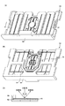
図2は、実施形態1に係る構造体の固定支持部材50の構成の一例を示した図である。図2において、固定支持部材50の構成の一例が、素子40とともに示されている。固定支持部材50は、素子40の固定枠30をパッケージに固定するために用いられる部品であり、その表面上に素子40が接着固定される。固定支持部材50は、固定枠30を表面上に載せて接着固定できるように、固定枠30よりも大きい周囲長を有する枠状に構成される。
FIG. 2 is a diagram illustrating an example of the configuration of the fixed
固定支持部材50は、枠状の部分にボス51を有する。枠状の部分は、素子40の固定枠30の下面との接着面を構成する。ボス51は、かかる素子40との接着面に設けられる。素子40と固定支持部材50との接着固定は、固定支持部材50又は素子40の接着面に接着剤を塗布し、両者を貼り合わせることにより行われる。その際、接着剤は、ボス51の存在する箇所以外は両者の隙間を充填するように、ボス51の周辺を含めて塗布される。接着剤は、種々の接着剤を用いることができるが、例えば、紫外線の照射により硬化する紫外線硬化接着剤を用いるようにしてもよい。また、接着剤は、その他、2液反応、熱、嫌気、湿気等により硬化する接着剤が用いられてもよく、種々の接着剤を使用することができる。なお、紫外線硬化接着剤を用いる場合には、固定支持部材50を介して接着剤に紫外線が照射できるように、固定支持部材50には紫外線を透過するような、例えば、透明な部材を用いることが好ましく、例えば、アクリル樹脂やポリカーボネート樹脂等の透明な樹脂成形部品を用いるようにしてもよい。その他の接着剤を用いる場合には、必ずしも透明な固定支持部材50を用いなくてもよく、用途に応じて種々の材料からなる部品を用いることができる。
The fixed
ボス51は、素子40と固定支持部材50とを接着固定したときに、素子40の電極パッド形成領域32に重なるように配置される。つまり、ボス51は、電極パッド41と対応する位置に設けられることになる。これは、素子40と固定支持部材50とを接着固定した後に、これを基板上に設置し、基板上に設けられた端子パッドとの超音波ボンディングを行うが、その際に、超音波が柔らかい接着剤層を伝わって逃げるのを防止する役割を果たす。よって、ボス51は、電極パッド31に対し超音波ボンディングを行う際に利用するものであるため、電極パッド形成領域32の下方にボス51が存在するように、電極パッド形成領域32と重なる位置に設けられる。
The
ボス51は、素子40の位置決め支持が可能なように、接着面に3個以上設けられることが好ましい。これにより、ボス51がスペーサのように機能し、素子40をボス51に載せて支持した状態で位置決めを行うことができる。配置にもよるが、接着面に少なくとも3点以上のボス51が配置されていれば、ボス51が素子40を支持した状態を作り出すことができる。この状態であれば、高さに関しては素子40の位置決めは不要となり、水平位置のみの位置決めでよくなるので、接着工程を容易に行うことが可能となる。なお、図2においては、ボス51は左右に各々2個ずつ設けられている。左右対称に素子40を支持することがバランス上好ましいので、図2に示すように、左右に2個ずつ、合計4個ボス51を設けるようにしてもよい。
It is preferable that three or
固定支持部材50は、素子40を下側から保護するために、耐衝撃用下側ストッパ52を有する。これにより、本実施形態に係る構造体が落下等により衝撃を受けた場合であっても、素子40を衝撃から保護することができる。
The fixed
図3は、実施形態1に係る構造体のボス51の構成の種々の例を示した側面図である。図3(A)は、実施形態1に係る構造体の固定支持部材50の第1の例に係るボス51の形状を示した図である。図3(A)に示すように、ボス51は、例えば、円柱の先端が上に凸の曲面状に構成された形状であってもよい。曲面は、例えば、半球状のような球の一部であってもよいし、上に凸の他の形状であってもよい。ボス51をこのような、先端部が上に凸の曲面状に構成することにより、素子40を最低限の接点で支持することができる。例えば、ボス51の高さが若干異なっていたような場合であっても、図3(A)の構成であれば、固定枠30とボス51は、制約の無い点接触となるので、何ら素子40に余分な応力を加えることなく素子40を支持することができる。
FIG. 3 is a side view showing various examples of the configuration of the
図3(B)は、固定支持部材50の第2の例に係るボス51Aの構成を示した図である。第2の例に係るボス51Aは、上面が平面の柱状の形状を有している。ボス51Aは、円柱状であってもよいし、三角柱や四角柱の角柱であってもよい。第2の例に係るボス51Aの場合には、複数個のボス51Aの高さを正確に合わせることが必要となるので、第1の例に係るボス51よりも、正確な高さの加工が要求される。
FIG. 3B is a diagram illustrating a configuration of a
図3(C)は、固定支持部材50の第3の例に係るボス51Bの構成を示した図である。第3の例に係るボス51Bは、形状は第1の例に係るボス51と同じであるが、隣接した左右のボス51Bの高さが異なる点で、第1の例に係るボス51と異なっている。例えば、素子40を傾斜させた状態で固定支持したい場合には、第3の例に係るボス51Bを用いて、素子40を支持するようにしてもよい。第3の例に係るボス51Bを用いた場合には、素子40の固定枠30はボス51Bに点接触で支持されるので、たとえ傾斜した状態で支持されても、余分な応力が素子40に加わることを防ぐことができる。
FIG. 3C is a diagram illustrating a configuration of a
このように、固定支持部材50のボス51、51A、51Bは、用途に応じて種々の形状に構成することができる。なお、以後の説明においては、第1の例に係るボス51を用いた例を挙げて説明する。
As described above, the
なお、今まで及び今後の説明において、素子40及び固定支持部材50は、ともに本実施形態に係る構造体の部品として機能するので、素子40を第1の部品40、固定支持部材50を第2の部品50と呼んでもよいこととする。
In the description so far and in the future, both the
図4は、本発明の実施形態1に係る構造体の素子40と固定支持部材50が接着固定した状態を示した図である。図4(A)は、実施形態1に係る構造体の素子40側(表面側)からの斜視図であり、図4(B)は、実施形態1に係る構造体の固定支持部材50側(裏面側)からの斜視図であり、図4(C)は、実施形態1に係る構造体の側面図である。
FIG. 4 is a diagram showing a state where the
図4(A)に示すように、固定支持部材50上に、素子40が接着固定されている。長さ及び幅の大きい固定支持部材50上に、素子40が搭載された状態となっている。
As shown in FIG. 4A, the
図4(B)に示すように、構造体の裏面には固定支持部材50が配置され、素子40の下側への動作を制約するように、耐衝撃用下側ストッパ52が素子40の主要部分をカバーしている。
As shown in FIG. 4B, a fixed
図4(C)に示すように、素子40と固定支持部材50との間には、接着剤60が存在し、素子40と固定支持部材50とを接着固定している。なお、接着剤60は、上述のように、紫外線硬化等の種々の硬化方法により硬化されてよいが、硬化後の接着剤60の軟度が比較的高く、固定支持部材50の熱変形を吸収できる軟度の柔らかい接着剤を用いる。これは、接着剤の硬化後に構造体が高温となり、固定支持部材50が変形しても、素子40を変形させないようにするためである。上述のように、素子40は、シリコン等の半導体材料から構成されることが多いが、固定支持部材50は、アクリルやポリカーボネート等の樹脂から構成される場合が多く、両者の熱膨張係数が異なる場合が多い。かかる材料構成の構造体に高温が加わると、固定支持部材50の変形の影響を素子40が受け、素子40の温度特性が低下する場合がある。そのような温度特性の低下を防止するため、本実施形態に係る構造体においては、固定支持部材50の変形による応力を吸収できる軟度の接着剤を、素子40と固定支持部材50との接着に用いるようにする。例えば、接着剤には、硬化後シェア硬度200以下(JIS−7215)のような柔らかい接着剤を用いるようにすることが好ましい。
As shown in FIG. 4C, an adhesive 60 exists between the
このように、柔らかい接着剤を用いることにより、本実施形態に係る構造体の温度特性を向上させることができる。なお、図4(C)において、ミラー11に入射光が照射され、ミラー11の揺動により、反射光が左右に2θずつ走査する例が示されている。
Thus, the temperature characteristic of the structure according to the present embodiment can be improved by using a soft adhesive. In FIG. 4C, an example is shown in which incident light is irradiated onto the
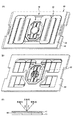
図5は、本発明の実施形態1に係る構造体の、基板70上に固定支持部材50と素子40が固定された状態を示した図である。図5(A)は、基板70上に固定支持部材50と素子40が固定された状態の構造体の構成の一例を示した斜視図である。図5(A)に示されるように、基板70の上に一体となった素子40及び固定支持部材50が固定される。基板70は、例えば、プリント基板等の樹脂製の基板が用いられてもよい。基板70上への素子40及び固定支持部材の固定は、種々の方法で行われてよいが、例えば、接着剤を用いた接着固定により行われてもよい。なお、ここで用いる接着剤は、素子40と固定支持部材50との接着に用いられた接着剤60とは異なる接着剤を用いてよい。つまり、基板70上に固定支持部材50の下面を接着する際には、用途に応じて種々の接着剤が用いられてよく、硬化度等の制約を特に有しない。
FIG. 5 is a diagram illustrating a state in which the fixed
基板70は、素子40の電極パッド31と隣接する位置に、端子パッド71を備えている。基板70上に素子40と一体化した固定支持部材50が接着された後は、素子40の電極パッド31と基板70の端子パッド71とがワイヤボンディングされて電気的に接続される。その際、ワイヤボンディングは、超音波振動を加えながら金属のワイヤ80(リード線)を端子パッド71及び電極パッド31に圧着する超音波ボンディングにより行われる。まず、端子パッド71にワイヤ80の一端を超音波ボンディングにより接合し、次いで、電極パッド31にワイヤ80の他端を超音波ボンディングにより接合する。ここで、素子40の電極パッド31にワイヤ80を超音波ボンディングする際、従来の構造体のように、素子40と固定支持部材50との間が柔らかい接着剤のみで充填されていると、超音波の振動が接着剤に吸収され、超音波振動を十分に電極パッド31に伝えることができない。しかしながら、本実施形態に係る構造体においては、素子40と固定支持部材50との間にボス51が存在するため、超音波振動が接着剤60によって吸収されることを防止でき、超音波振動を十分に電極パッド31に伝えることができる。
The
図5(B)は、ボス51付近の構造体の断面構成の一例を示した図である。図5(B)において、半導体基板70上に、接着剤65と、固定支持部材50と、ボス51及び接着剤60と、素子40とが順に下から積層されている。また、素子40の表面には、電極パッド形成領域32内に電極パッド31が形成されている。かかる構成において、電極パッド31上に超音波ボンディングが行われると、電極パッド31に印加された超音波振動は、素子40がボス51で固定されているために、接着剤60から逃げてゆかずに、素子40を直接的に振動させることができる。つまり、超音波ボンディングの際に、超音波振動により接着剤60は柔らかくなるが、ボス51が素子40を固定しているため、超音波振動を素子40に伝達させ、素子40を振動させることができる。これにより、電極パッド31上へのワイヤボンディングを問題無く行うことができ、電極パッド31と端子パッド71とをワイヤ80により電気的に接続することができる。
FIG. 5B is a diagram showing an example of a cross-sectional configuration of the structure near the
ここで、ボス51を設けずに、代わりとして硬い接着剤60を用いれば、ワイヤボンディング自体は行うことができる。しかしながら、硬い接着剤60を用いると、温度が高温となり、固定支持部材50が変形したときに、その変形を、接着剤60を介して素子40に伝達してしまうので、構造体の温度特性が悪くなってしまう。そこで、本実施形態に係る構造体のように、接着剤60は応力を吸収できる柔らかい接着剤60を用い、固定支持部材50の素子40との接着面にボス51を設けるようにすれば、良好な温度特性を実現しつつ、超音波ボンディングも適切に行うことができる。
Here, if the
なお、図5(B)において、基板70と固定支持部材50との間にも接着剤65が存在するが、上述のように、この接着剤65には任意の接着剤65を用いることができる。基板70上の端子パッド71への超音波ボンディングには接着剤65は全く関与していないし、電極パッド31の超音波ボンディングの際にも、超音波の振動が接着剤65まで到達してこれを軟化させ、振動が逃げる状態とすることは考え難いからである。
In FIG. 5B, the adhesive 65 is also present between the
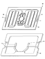
図6は、本発明の実施形態1に係る構造体のパッケージング完成状態を示した図である。図6(A)は、実施形態1に係る構造体のパッケージング完成状態を示した図である。図6(A)において、カバー90が、基板70を上面から覆った状態が示されている。このように、基板70上に固定された固定支持部材50及び素子40は、カバー90に覆われてパッケージングされる。カバー90は、上面に位置決めボス91と、透明板100とを備える。位置決めボスは、光走査装置として構成された本実施形態に係る構造体を、プロジェクタユニット等に取り付ける際に位置決めを行うための嵌合手段である。また、透明板100は、素子40のミラー11が設置される位置に設けられる。透明板100は、例えば、両面に反射防止膜が設けられた両面反射防止膜付きの透明板100として構成されてもよい。
FIG. 6 is a diagram illustrating a packaging completion state of the structure according to the first embodiment of the present invention. FIG. 6A is a diagram illustrating a packaging completion state of the structure according to the first embodiment. FIG. 6A shows a state where the
図6(B)は、実施形態1に係る構造体のパッケージング状態の側断面斜視図であり、図6(C)は、実施形態1に係る構造体のパッケージング状態の側断面である。図6(C)において、下から順に基板70、固定支持部材50、接着剤60、素子40及びカバー90が積層された構成が示されている。また、カバー90は、素子40の上側に耐衝撃用上側ストッパ92を有し、落下等の衝撃が加わった場合にも、素子40の破損を防止できる構成となっている。また、カバー90の中央表面には、透明板100が設けられており、ミラー11を保護している。
6B is a side sectional perspective view of the structure according to the first embodiment in a packaging state, and FIG. 6C is a side sectional view of the structure according to the first embodiment in a packaging state. FIG. 6C shows a configuration in which the
図6(D)は、カバー90の裏面の構造を示した斜視図である。図6(D)において、耐衝撃用上側ストッパ92の構成が示されている。このように、カバー90は、耐衝撃用上側ストッパ92を有し、パッケージングにより内部の素子40を衝撃から保護する構成を有してよい。
FIG. 6D is a perspective view showing the structure of the back surface of the
図6(E)は、基板70の裏面を示した図である。図6(E)に示されるように、基板70の裏面には、電極72が設けられている。電極72は、表面側の端子パッド71と導通し、電極72から端子パッド71を介して内部の素子40に電力が供給できる構成となっている。
FIG. 6E is a view showing the back surface of the
実施形態1に係る構造体は、MEMS技術を用いて微小構造体として構成され得るので、例えば、実施形態1に係る構造体のパッケージサイズは、高さ7.0mm×幅11.5mm×奥行2.4mmのレベルの大きさで構成することができる。 Since the structure according to the first embodiment can be configured as a microstructure using the MEMS technology, for example, the package size of the structure according to the first embodiment is 7.0 mm high × 11.5 mm wide × 2 deep. .4mm level size can be configured.
実施形態1に係る構造体によれば、積層のみの容易なプロセスにより、温度特性が良好で、超音波ボンディングを適切に行うことができ、高精度な構造体とすることができる。 According to the structure according to the first embodiment, the temperature characteristics are good, ultrasonic bonding can be appropriately performed, and a highly accurate structure can be obtained by an easy process including only lamination.
〔実施形態2〕
図7は、本発明の実施形態2に係る構造体の素子の構成を説明するための図である。実施形態2に係る構造体は、実施形態1と同様に、光走査装置として構成した構造体について説明する。また、実施形態1と同様の構成要素については、同一の参照符号を付し、その説明を省略する。
[Embodiment 2]
FIG. 7 is a diagram for explaining a configuration of an element of a structure according to Embodiment 2 of the present invention. As in the first embodiment, the structure according to the second embodiment will be described as a structure configured as an optical scanning device. Moreover, about the component similar to Embodiment 1, the same referential mark is attached | subjected and the description is abbreviate | omitted.
図7(A)は、素子41の構成を示した斜視図である。図1(A)において、素子41は、水平駆動部10及び垂直駆動部20を備え、周囲が固定枠33で囲まれている点で、実施形態1に係る構造体の素子40と同様である。
FIG. 7A is a perspective view showing the configuration of the
図7(B)は、実施形態2に係る構造体の素子42の構成の一例を示した斜視図である。図7(B)に示した素子42は、図7(A)に示した素子41から、左右両側と奥側の固定枠33が除去され、固定枠の1辺分の固定片34のみとなっている。また、電極パッド35は、固定枠34の中央付近の電極パッド形成領域36内に設けられている。電極パッド35は、実施形態1に係る構造体において、固定枠30の両側に半分ずつ設けられていたものを、実施形態2に係る構造体においては、中央付近の1箇所の電極パッド形成領域36内に設けているので、2倍のスペースを有し、内側に凸の平面形状を有している。
FIG. 7B is a perspective view showing an example of the configuration of the
このように、実施形態2に係る構造体においては、素子42を支持する部分を、固定片34のみの最低限とし、面積の小さい素子42を構成する。素子42は、半導体から構成されるので、1枚の半導体ウェハからの素子42の取り数を多くすることができ、低コストで構造体を構成することが可能となる。実施形態2に係る構造体は、このような、低価格/小型素子パッケージングの構造体の例について説明する。
As described above, in the structure according to the second embodiment, the portion that supports the
図8は、実施形態2に係る構造体の固定支持部材53を、素子42とともに示した図である。図8において、固定支持部材53は、固定片34に対応して、1辺のみを支持する形状となっている。また、固定支持部材53は、素子42の固定片34の電極パッド形成領域36内に設けられた電極パッド35に対応する位置に、ボス54を3個備えている。ボス54は、固定支持部材53と素子42とが接着固定したときに、電極パッド35と重なる位置に設けられている。これにより、実施形態1と同様に、後のボンディング工程で、電極パッド35への超音波ボンディングを確実に行うことができる。
FIG. 8 is a view showing the fixed
また、ボス54は、実施形態1とは異なり、3個だけ設けられている。実施形態2に係る構造体においては、電極パッド35が1箇所に集約され、電極パッド形成領域36が狭くなったので、それに対応してボス54の数も最低限の3個としている。ボス54の形状は、図3において説明したように、種々の形状で構成されてよい。
Further, unlike the first embodiment, only three
なお、素子42と固定支持部材53との接着を紫外線硬化接着剤で行う場合には、固定支持部材53が、アクリル樹脂やポリカーボネート樹脂等の透明な樹脂成形部品で構成される点は、実施形態1に係る構造体と同様である。
In the case where the
固定支持部材53は、耐衝撃用下側ストッパ55を有し、構造体が落下等により衝撃を受けたときに、素子42を保護する構成となっている点も、実施形態1に係る構造体と同様である。
The fixed
図9は、実施形態2に係る構造体の素子42と固定支持部材53とが接着固定されて一体となった状態を示した図である。図9(A)は、実施形態2に係る構造体の素子42と固定支持部材53とが接着固定されて一体となった状態の素子42側(表面側)からの斜視図である。図9(A)において、素子42が、固定片34の部分を固定支持部材53の奥に突き当てるように挿入されて接着固定されることが分かる。電極パッド形成領域36と重なる固定支持部材53の接着面上には、ボス54が存在することになる。
FIG. 9 is a diagram illustrating a state in which the
図9(B)は、実施形態2に係る構造体の素子42と固定支持部材53とが接着固定されて一体となった状態の固定支持部材53側(裏面側)からの斜視図である。図9(B)に示されるように、素子42は、固定支持部材53により、手前側で片持ち支持されており、裏面は耐衝撃用下側ストッパ55でガードされていることが分かる。
FIG. 9B is a perspective view from the fixed
図9(C)は、実施形態2に係る構造体の素子42と固定支持部材53とが接着固定されて一体となった状態の側面図である。図9(C)に示されるように、固定支持部材53の根元部分と、素子42の固定片34の部分とが接着剤61で接着固定されている。最も下段には耐衝撃用下側ストッパ55があり、固定支持部材53の根元部分の上面に、素子42が接着剤61で接着固定されている。更に、固定支持部材53は、上下から素子42を挟み込むような形状となっているので、素子43の上面にある固定支持部材53の底面部分と、素子43の上面との間も接着剤61により接着固定された構成となっている。このように、実施形態2に係る構造体においては、素子42を固定支持部材53で上下から挟み込むように接着剤61で接着固定してよい。
FIG. 9C is a side view showing a state in which the
なお、接着剤61として、高温となり固定支持部材53が変形したときに、これにより発生する応力を吸収し、素子42に影響を与えないような軟度を有する接着剤61が用いられる点は、実施形態1と同様である。また、例えば、接着剤61には、硬化後シェア硬度200以下(JIS−K−7215)の柔らかい接着剤61を用いてもよいことも、実施形態1に係る構造体と同様である。かかる柔らかい接着剤61で素子42と固定支持部材53を接着固定した構成とすることにより、実施形態2に係る構造体の温度特性を向上させることができる。
Note that the adhesive 61 has such a softness that it absorbs the stress generated by the fixing
図10は、実施形態2に係る構造体の、基板73上に固定支持部材53及び素子42が固定された状態を示した斜視図である。図10において、基板73上に固定支持部材53及び素子42が接着固定され、素子42の電極パッド35と基板73の端子パッド74とがワイヤ81により接続されている。かかるワイヤ81を用いたワイヤボンディングは、実施形態1と同様に、超音波ボンディングにより行われてよい。超音波ボンディングは、ワイヤ81を、超音波振動を印加しながら端子パッド74及び電極パッド35に圧着することにより行われる。電極パッド35への超音波ボンディングは、固定支持部材53の素子42との接着面に設けられたボス54により、超音波振動を接着剤61に逃がすことなく行うことができ、適切に超音波ボンディングによる接合を行うことができる。
FIG. 10 is a perspective view illustrating a state in which the fixed
実施形態2に係る構造体においても、基板73側の端子パッド74と素子42側の電極パッド35は隣接した位置となり、ワイヤボンディングを最小限のワイヤ81により行うことができる。このように、低価格/小型素子パッケージとして構成した実施形態2に係る構造体においても、超音波ボンディング自体は、実施形態1に係る構造体と同様に適切に行うことができる。
Also in the structure according to the second embodiment, the
図11は、実施形態2に係る構造体のパッケージング完成後の構成を示した図である。図11(A)は、実施形態2に係る構造体のパッケージング完成後の全体構成を示した斜視図である。図11(A)に示されるように、実施形態2に係る構造体においても、カバー93が素子42、固定支持部材53及び基板73を覆った構成となっている。また、カバー93の表面に、プロジェクタユニットへの取り付け位置決めボス94が設けられている点と、中央に透明板100が用いられている点も、実施形態1に係る構造体と同様である。
FIG. 11 is a diagram illustrating a configuration after the packaging of the structure according to the second embodiment is completed. FIG. 11A is a perspective view showing an overall configuration after completion of packaging of the structure according to the second embodiment. As shown in FIG. 11A, in the structure according to the second embodiment, the
図11(B)は、実施形態2に係る構造体のパッケージング完成後の断面構成を示した斜視図であり、図11(C)は、実施形態2に係る構造体のパッケージング完成後の断面構成を示した側断面図である。図11(C)において、下から順に、基板73、固定支持部材53、接着剤61、素子42及びカバー93が積層されている。また、カバー93の内部であって、素子42の上方には、耐衝撃用上側ストッパ95が設けられ、素子42を上側から保護するようになっている。また、中央部に、透明板100が設けられている点も、実施形態1と同様である。
FIG. 11B is a perspective view showing a cross-sectional configuration after the packaging of the structure according to the second embodiment is completed, and FIG. 11C is a diagram after the packaging of the structure according to the second embodiment is completed. It is the sectional side view which showed the cross-sectional structure. In FIG. 11C, a
図11(D)は、カバー93の裏面の構成を示した図であり、3方のみを覆うように構成されている点で、実施形態1と異なっている。耐衝撃用上側ストッパ95が、素子42の設置位置に対応して設けられている点も、実施形態1に係る構造体と同様である。
FIG. 11D is a diagram showing the configuration of the back surface of the
図11(E)は、実施形態2に係る構造体のパッケージング完成後の裏面側を示した図である。図11(E)において、電極75が基板73の裏面に用いられ、ここから素子42との導通を図れる点も、実施形態1に係る構造体と同様である。
FIG. 11E is a view showing the back surface side after the packaging of the structure according to the second embodiment is completed. In FIG. 11E, the
実施形態2に係る構造体は、図7(A)に示した構成の素子41を、実施形態1に係る構造体の素子40と同様なサイズで構成し、その後の加工を行うと、高さ7.0mm×幅10.0mm×奥行2.4mmのパッケージングで構成することができ、実施形態1に係る構造体のパッケージングよりも、幅を1.5mm減少させることができる。
The structure according to the second embodiment is configured such that the
実施形態2に係る構造体によれば、低コスト、小型に構成できる構造体においても、温度特性を向上させるとともに、超音波ボンディングにより適切にワイヤボンディングを行うことができる。 According to the structure according to the second embodiment, the temperature characteristics can be improved and wire bonding can be appropriately performed by ultrasonic bonding even in a structure that can be configured at low cost and in a small size.
〔実施形態3〕
図12は、本発明の実施形態3に係る構造体の素子の構成を説明するための図である。実施形態3においては、低背化パッケージングの構造体の例について説明する。なお、実施形態1に係る構造体と同様の構成要素については、同一の参照符号を付してその説明を省略する。図12(A)は、実施形態1に係る構造体の素子40と同様の構成が示した図であり、図12(B)は、実施形態3に係る構造体の素子43の構成の一例を示した図である。
[Embodiment 3]
FIG. 12 is a diagram for explaining a configuration of an element of a structure according to
図12(A)に示した素子40の固定枠30から、手前側と奥側の部分を除去すると、図12(B)に示した実施形態3に係る構造体の素子43となる。実施形態3に係る構造体の素子43は、垂直駆動部20の両側にのみ固定部材37を備えた構成となっている。また、電極パッド31は、左右の固定部材37の中央の電極パッド形成領域32内に各々設けられた構成となっている。
When the front and back portions are removed from the fixed
図13は、実施形態3に係る構造体の固定支持部材56を、素子43とともに示した図である。固定支持部材56は、奥側の辺に対応する部材を有しない、3辺を囲んだ構成となっている。固定支持部材56は、素子43の電極パッド31に対応するように、上面にボス57を備えている。ボス57は、実施形態1と同様に、両側に2個ずつ設けられている。また、固定支持部材56の中央付近には、耐衝撃用下側ストッパ58が設けられている。なお、ボス57の形状は、種々の構成をとりうることは、図3において説明した通りである。
FIG. 13 is a view showing the fixed
図14は、実施形態3に係る構造体において、素子43と固定支持部材56とを接着固定した状態を示した図である。図14(A)は、実施形態3に係る構造体において、素子43と固定支持部材56とを接着固定した状態を素子43側(表面側)から示した斜視図である。図14(A)に示されるように、素子43が、固定支持部材56の手前側の側面に突き当たるまで挿入された状態で接着固定されている。素子43は、固定支持部材56の接着面上に設置され、ボス57が電極パッド31と重なる位置で接着固定される。
FIG. 14 is a view showing a state in which the
図14(B)は、実施形態3に係る構造体において、素子43と固定支持部材56とを接着固定した状態を固定支持部材56側(裏面側)から示した斜視図である。図14(B)に示されるように、素子43の裏面を、耐衝撃用下側ストッパ58がカバーしており、素子43が落下等により衝撃を受けた場合であっても、耐衝撃用下側ストッパ58がクッションの役割を果たすように構成されている。
FIG. 14B is a perspective view showing a state in which the
図14(C)は、実施形態3に係る構造体において、素子43と固定支持部材56とを接着固定した状態の側面図である。図14(C)において、下側の固定支持部材56と素子43が接着剤62により接着され、素子43の上面端部を固定支持部材56が上下から挟むように覆った構成となっている。実施形態1において説明したように、接着剤62は、固定支持部材56が高温により変形しても、変形による応力を吸収できるような柔らかい軟度を有する接着剤62を用いるようにする。具体的には、例えば、硬化後シェア硬度200以下(JIS−K−7215)の柔らかい接着剤62を用いるようにする。これにより、温度特性の高い構造体とすることができる。
FIG. 14C is a side view showing a state in which the
図15は、実施形態3に係る構造体の、基板上に固定支持部材56及び素子43が固定された状態を示した図である。図15に示すように、固定支持部材56上に素子43が接着剤62で接着固定された部品が、基板76上に設置されて接着固定される。この場合に用いる接着剤は、任意の接着剤を用いることができる。基板76上に、固定支持部材56及び素子43が接着固定された後は、基板76に設けられた端子パッド77と、素子43の電極パッド31とを、ワイヤ82を用いて超音波ボンディングにより接続する。このとき、実施形態1で説明したように、電極パッド31の下面は、ボス57で支持されているので、接着剤61を介して超音波振動が逃げることもなく、適切にワイヤボンディングを行うことができる。
FIG. 15 is a diagram illustrating a state in which the fixed
図16は、実施形態3に係る構造体のパッケージング完成後の構成を示した図である。図16(A)は、実施形態3に係る構造体のパッケージング完成後の全体構成を示した斜視図である。図16(A)に示されるように、基板77上に接着固定された固定支持部材56及び素子43は、カバー96により覆われる。カバー96は、中央部に凹形状を有し、固定支持部材56の手前中央部の凸形状と嵌合する構成となっている点が、実施形態1及び実施形態2に係る構造体のカバー90、93と異なっている。かかる嵌合構造により、構造体のパッケージングの高さを低く構成することができる。
FIG. 16 is a diagram illustrating a configuration after packaging of the structure according to the third embodiment. FIG. 16A is a perspective view showing an overall configuration after completion of packaging of the structure according to the third embodiment. As shown in FIG. 16A, the fixing
なお、カバー96の上面にプロジェクタユニットへの取り付け用の位置決めボス98が複数設けられ、中央部には両面反射防止膜付きの透明板100が設けられている点は、実施形態1及び実施形態2に係る構造体と同様である。
The first embodiment and the second embodiment are that a plurality of
図16(B)は、実施形態3に係る構造体のパッケージング完成後の断面構成を示した斜視図であり、図16(C)は、実施形態3に係る構造体のパッケージング完成後の断面構成を示した側断面図である。図16(C)において、下から順に基板76、固定支持部材56、接着剤62、素子43、カバー96が積層された構成が示されている。また、カバー96の内面であって、素子43の上方には耐衝撃用上側ストッパ99が設けられ、構造体に落下や衝突等により衝撃が加わっても、素子43を保護する構成となっている。また、カバー96の中央の表面には、透明板100が設置されている。光は、透明板100を介して素子43のミラー11に照射される。
FIG. 16B is a perspective view showing a cross-sectional configuration after the packaging of the structure according to the third embodiment is completed, and FIG. 16C is a diagram after the packaging of the structure according to the third embodiment is completed. It is the sectional side view which showed the cross-sectional structure. FIG. 16C shows a configuration in which a
図16(D)は、カバー96の裏面の構成を示した図である。カバー96の手前側の側面には、凹形状が設けられ、固定支持部材56との嵌合により高さを低減させる構成となっている。また、耐衝撃用上側ストッパが設けられている点は、実施形態1及び実施形態2に係る構造体のカバー90、93と同様である。
FIG. 16D is a diagram showing the configuration of the back surface of the
図16(E)は、実施形態3に係る構造体のパッケージング完成後の裏面側の構成の一例を示した図である。構造体の裏面には、基板77が配置され、基板77の裏面には、電極78が設けられている。電極78を介して、素子43に電力を供給して構造体を駆動させる点は、実施形態1及び実施形態2に係る構造体と同様である。
FIG. 16E is a diagram illustrating an example of the configuration on the back surface side after the packaging of the structure according to the third embodiment is completed. A
実施形態3に係る構造体のパッケージングは、図12(A)で示した素子のサイズを実施形態1と同様のサイズとした場合、高さ6.0mm×幅11.5mm×奥行2.4mmで構成することができ、高さを1.0mm低減することができる。 In the packaging of the structure according to the third embodiment, when the size of the element shown in FIG. 12A is the same as that of the first embodiment, the height is 6.0 mm × the width is 11.5 mm × the depth is 2.4 mm. The height can be reduced by 1.0 mm.
このように、実施形態3に係る構造体によれば、温度特性が高く、超音波ボンデシィングを適切に行えるとともに、高さの低いパッケージングを構成することができる。 Thus, according to the structure according to the third embodiment, the temperature characteristics are high, ultrasonic bonding can be performed appropriately, and a low-height packaging can be configured.
〔実施形態4〕
図17は、本発明の実施形態4に係る構造体の素子の一例を示した構成図である。図17において、実施形態1乃至3と同様の構成要素には、同一の参照符号を付し、その説明を省略する。
[Embodiment 4]
FIG. 17 is a configuration diagram illustrating an example of an element of a structure according to Embodiment 4 of the present invention. In FIG. 17, the same components as those in the first to third embodiments are denoted by the same reference numerals, and the description thereof is omitted.
図17において、実施形態4に係る構造体の素子44は、水平駆動部16と、垂直駆動部24と、固定部材37とを有する。
In FIG. 17, the
水平駆動部16は、ミラー11と、捻れ梁17と、スリット18と、水平駆動梁14と、駆動源15とを有する点で、実施形態1乃至3に係る構造体の素子40〜43と共通するが、捻れ梁17の細長く延在した部分にスリット18が形成されておらず、ミラー11の周辺部分にスリット18が形成されている点で、実施形態1乃至3に係る構造体の素子40〜43と異なっている。かかるスリット18は、捻れ梁17のミラー近くの部分の捻れによる応力を緩和し、捻れ梁17のミラー付近の破損を防ぐ構造となっている。このように、水平駆動部16の構成は、用途に応じて種々の構成とすることができる。なお、ミラー11、水平駆動梁14及び駆動源15は、実施形態1乃至3に係る構造体の素子40〜43と同様であるので、同一の参照符号を付してその説明を省略する。
The
垂直駆動部24は、垂直駆動梁26の直線部分が片側3本ではなく、片側4本となっている点で、実施形態1乃至3に係る構造体の素子40〜43と異なっている。また、可動枠25の大きさが大きくなり、間隔を有して水平駆動部16を囲んだ構成となっている点も実施形態1乃至3と異なっている。垂直駆動梁26の各直線部の表面に駆動源23が設けられている点は、実施形態1乃至3に係る構造体の素子40〜43と同様である。
The
図17に示すように、垂直駆動梁26を4ピース構成とすることにより、垂直駆動部24の面積は少し増加するものの、ミラー11の両側で位相の異なる駆動梁が常に同数となり、垂直方向の揺動の角度の大きさを、手前側への傾斜と奥側への傾斜で同じにすることができる。このように、垂直駆動部24についても、用途に応じて多様な構成をとることができる。
As shown in FIG. 17, although the
固定部材37は、垂直駆動梁26との接続位置が反対側であるものの、その形状、構成は実施形態3に係る構造体の素子43の固定部材37と同様であるので、同一の参照符号を付してその説明を省略する。また、電極パッド31及び電極パッド形成領域32も実施形態1乃至3に係る構造体の素子40〜43と同様であるので、同一の参照符号を付してその説明を省略する。
Although the fixing
図18は、実施形態4に係る構造体のパッケージの一例を示した図である。図18(A)は、実施形態4に係る構造体のパッケージの上面斜視図であり、図18(B)は、実施形態4に係る構造体のパッケージの下面斜視図である。 FIG. 18 is a diagram illustrating an example of a package of a structure according to the fourth embodiment. 18A is a top perspective view of the package of the structure according to the fourth embodiment, and FIG. 18B is a bottom perspective view of the package of the structure according to the fourth embodiment.
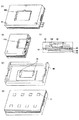
図18(A)において、パッケージ110は、底部111と、位置決めマーク112と、素子固定部113と、接着部材114と、端子パッド115と、取り付け部116とを有する。パッケージ110は、図17に示した素子44をパッケージングするための収容部材であり、パッケージ110の上面側に素子44が固定取り付けされる。パッケージ110は、材料は、用途に応じて種々の材料が用いられてよいが、例えば、セラミックスが用いられてもよい。
In FIG. 18A, a
底部111は、素子44と所定間隔を保ち、ミラー11が揺動する深さ方向のスペースを確保するために、素子固定部113よりも窪んだ凹形状に形成される部分である。よって、素子44は、底部111に接触しない状態でパッケージ110に保持される。なお、底部111は、図18に示すように、平面で構成されていてもよいし、耐衝撃用下側ストッパを設ける場合には、更に中心を深く掘って溝を形成するか凸状として突き出して構成してもよい。
The
位置決めマーク112は、素子44を取り付けてパッケージングする際、ミラー11の位置が中心に来るように位置決めを行うための基準となる目印である。つまり、ミラー11の中心が位置決めマーク12の中心の十字の部分と一致するように素子44が取り付けられる。
The
素子固定部113は、素子44を載置して固定する部分であり、底部111よりも隆起した水平面となっている。素子固定部113上に素子44の固定部材37が載置され、接着剤等で接着又は接合されて固定される。
The
素子固定部113は、接着部材114と、端子パッド115とを備える。接着部材114は、素子固定面、つまり接着面に設けられる部材であり、例えば、実施形態1乃至3に係る構造体のボス51、54、57と同様に、突起した形状のボスが用いられてもよいし、突起というよりも周囲から少し盛り上がって隆起した程度の隆起部材であってもよい。また、接着部材114は、接着の位置合わせに用いられるような突起、窪み、溝等であってもよく、接着面に設けられ、接着のため、又は接着に関連して用いられる種々の部材であってよい。図18(A)においては、各素子固定部113の中央部分に、2つのボス状の接着部材114がそれぞれ設けられている。これにより、実施形態1乃至3と同様に、超音波ボンディングを適切に行うことができる。なお、接着部材114の数や位置は、用途に応じて種々変更できるが、超音波ボンディングの際に用いるため、素子44の電極パッド31が載置される位置に設けるようにする。結果的に、接着部材114は、端子パッド115と隣接する位置に設けられることになる。
The
端子パッド115は、素子44の電極パッド31と電気的に接続するための端子である。これにより、外部との電気的接続が可能となる。
The
取り付け部116は、素子44を収容保持したパッケージ110を、筐体等の所定の取り付け位置に取り付けるための接合部である。例えば、筐体の板状又は壁状の部分に取り付ける場合には、取り付け部116を筐体の所定の取り付け位置に接合することにより、筐体と素子44とが、取り付け部116の高さ分の間隔を保った状態で取り付けることができる。これにより、ミラー11が揺動する高さ方向のスペースを確保でき、素子44を適切に固定支持することができる。
The
また、取り付け部116は、パッケージ110の短手方向において、端子パッド115の両外側に設けられ、端子パッド115の配置及び電気的接続を妨げないような構成となっている。これにより、素子44の電極パッド31と端子パッド115は、中央部分で電気的接続を行うことができ、適切な電気的接続を行う構成を確保しつつ、筐体等への取り付けを行うために取り付け部116を設けることができる。
In addition, the
取り付け部116は、左右方向の片側に2つずつ設けられ、全体で4つ設けられている。パッケージ110を、筐体の所定箇所に取り付ける場合、取り付け部116は最低3つあれば足りるが、上述のように、端子バッド115を短手方向の中央部に設ける場合には、端子パッド115の両側に取り付け部116を設け、電気的配線と筐体への固定取り付けの双方の機能を実現している。
Two
また、取り付け部116は、両側の短手方向に延在するレールのような形状で、全体で2つのみとして設けることも可能であるが、この場合には、端子パッド115を周縁部に設けることができなくなる。よって、本実施形態においては、端子パッド115の両側に2つずつ取り付け部116を設け、全体として4つ取り付け部116を設ける構成としている。
In addition, the
このように、パッケージ110は、素子固定部113を中間段として、素子固定部113よりも低い底部111及び素子固定部113よりも高い取り付け部116を備えることにより、ミラー11の上下にミラー11が揺動できるスペースを確保することができ、素子44が適切に動作できる状態で素子44をパッケージングし、筐体へ取り付けることが可能となる。
In this manner, the
図18(B)は、パッケージ110の裏面117を示している。パッケージ110の裏面117には、外部接続端子118が複数設けられており、外部との接続が可能な構成となっている。外部接続端子118は、上面側の端子パッド115と電気的に接続され、素子44と電気的に接続できるように構成されている。
FIG. 18B shows the
図19は、実施形態4に係る構造体のパッケージ110の各面を示した図である。図19(A)は、パッケージ110の上面図である。図18(A)において説明したように、パッケージ110の上面には、中央領域に底部111、それよりも外側の左右に素子固定部113、更に素子固定部113よりも外側の四隅に取り付け部116が設けられている。また、取り付け部116は、パッケージ110の短手方向の中央部に設けられている端子パッド115を回避して、端子パッド115を両外側から挟むように設けられ、端子パッド115の電気的接続を妨げない構成となっている。取り付け部116と端子パッド115は、パッケージ110の短手方向において一直線上に設けられているので、両者が干渉しないように、端子パッド115の両側に取り付け部116が配置された構成とされている。接着部材114は、端子パッド115に隣接して設けられ、素子44の超音波ボンディングを容易に行うことができるように構成されている。
FIG. 19 is a diagram illustrating each surface of the
図19(B)は、パッケージ110の側面図である。図19(B)に示すように、取り付け部116は、素子固定部113より高い構成となっている。
FIG. 19B is a side view of the
図19(C)は、パッケージ110の正面図である。図19(C)に示されるように、パッケージ110は、最も低い底部111と、中間の素子固定部113と、取り付け部116とからなる3段の平坦面を有する構成となっている。
FIG. 19C is a front view of the
図19(D)は、パッケージ110の底面図である。パッケージ110の底面117には、複数の端子118が設けられていることが分かる。
FIG. 19D is a bottom view of the
図20は、本発明の実施形態4に係る構造体を示した図である。図20において、素子44がパッケージ110にパッケージングされた状態が示されている。図20に示すように、素子固定部113上に両端が載置されるように素子44が設けられ、素子44の固定部材37の部分のみが、素子固定部113に接触して接合(接着)されている。これにより、素子44は、固定部材37で固定されるものの、ミラー11、水平駆動梁14を含む水平駆動部16、及び垂直駆動梁26を含む垂直駆動部26はフリーな状態となり、制約無く機械的駆動を行うことができる。また、素子44は、両側を4つの取り付け部116で囲まれ、外部から保護された状態で保持されるとともに、取り付け部116の上面を接合することにより、任意の箇所に取り付け可能な構成となっている。
FIG. 20 is a view showing a structure according to Embodiment 4 of the present invention. In FIG. 20, a state in which the
図21は、本発明の実施形態4に係る構造体の一例を示した図である。図21(A)は、実施形態4に係る構造体の上面図であり、図21(B)は、実施形態4に係る構造体の正面図である。 FIG. 21 is a view showing an example of a structure according to Embodiment 4 of the present invention. FIG. 21A is a top view of the structure according to the fourth embodiment, and FIG. 21B is a front view of the structure according to the fourth embodiment.
図21(A)において、実施形態4に係る構造体は、素子44の両側を取り付け部116及び端子パッド115が囲んでいる。端子パッド115と素子44の電極パッド31は隣接し、図示しないワイヤにより両者が電気的に接続されている。電極パッド44と端子パッド115が隣接しているため、短いワイヤで両者を接続することができる。また、電極パッド31及び端子パッド115の双方を覆うように、ワイヤ保護樹脂120が形成されている。なお、図21(A)において、ワイヤ保護樹脂120は透過的に示されている。ワイヤ保護樹脂120を設けることにより、外部のゴミや埃等から電極パッド44、ワイヤ及び端子パッド115を保護することができる。
In FIG. 21A, in the structure according to the fourth embodiment, the
図21(B)において、素子44とパッケージ110との高さの関係が示されている。素子44は、素子固定部113に支持されている。端子パッド115と電極パッド31は、ワイヤ保護樹脂120に覆われていることが分かる。
FIG. 21B shows the height relationship between the
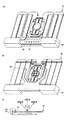
図22は、実施形態4に係る構造体を取り付け板に取り付けた状態の一例を示した図である。図22(A)は、実施形態4に係る構造体を取り付け板に取り付けた状態の内側の斜視図であり、図22(B)は、実施形態4に係る構造体を取り付け板に取り付けた状態の外側の斜視図である。 FIG. 22 is a diagram illustrating an example of a state in which the structure according to Embodiment 4 is attached to the attachment plate. FIG. 22A is a perspective view of the inside of the state in which the structure according to Embodiment 4 is attached to the attachment plate, and FIG. 22B is the state in which the structure according to Embodiment 4 is attached to the attachment plate. FIG.
図22(A)において、取り付け板140に、パッケージ110が取り付けられた状態が示されている。図22(A)に示すように、パッケージ110の取り付け部116の上面が取り付け板140に接触するように接着され、パッケージ110が取り付け板に取り付けされる。なお、パッケージ110の裏面には、更にフレキシブルプリント回路130が設けられ、パッケージ110の裏面の外部接続端子118に対応した端子131が設けられている。
FIG. 22A shows a state where the
図22(B)において、取り付け板140に開口141が設けられ、ミラー11で反射する光が、開口141を通って照射できるように構成されている。このように、パッケージ110が取り付けられる取り付け板140には、光を通すための開口141が設けられて構成される。
In FIG. 22B, the mounting
図23は、実施形態4に係る構造体を取り付け板に取り付けた状態の分解斜視図である。図23(A)は、実施形態4に係る構造体を取り付け板に取り付けた状態の内側からの分解斜視図であり、図23(B)は、実施形態4に係る構造体を取り付け板に取り付けた状態の外側からの分解斜視図である。 FIG. 23 is an exploded perspective view of a state in which the structure according to Embodiment 4 is attached to a mounting plate. FIG. 23A is an exploded perspective view from the inside of a state in which the structure according to the fourth embodiment is attached to the mounting plate, and FIG. 23B is a diagram in which the structure according to the fourth embodiment is attached to the mounting plate. It is a disassembled perspective view from the outer side of a state.
図23(A)において、取り付け板140に対して、素子44、パッケージ110、フレキシブルプリント回路130の順で取り付けられていることが示されている。フレキシブルプリント回路130の端子131は、パッケージ110の外部接続端子118に対応した箇所に設けられていることが分かる。
FIG. 23A shows that the
図23(B)は、図23(A)と反対側の状態を示した図である。取り付け板140の開口141内に素子44のミラー11が配置されるように、素子44、パッケージ110及びフレキシブル印刷回路が順次積層されて設けられていることが分かる。
FIG. 23B is a diagram showing a state on the opposite side to FIG. It can be seen that the
図24は、実施形態4に係る構造体を筐体に取り付けた一例を示した図である。図24(A)は、実施形態4に係る構造体を筐体145の取り付け板140に取り付けた箇所の拡大図である。図24(A)に示すように、筐体145の内部に仕切り板のように取り付け板140が設けられている。そして、筐体145の先端には、光を透過するカバー142が設けられている。実施形態4に係る構造体は、ミラー11からの反射光がカバー142を通過するように、取り付け板140に取り付けられている。筐体145は、例えば、プロジェクタの筐体であってもよい。
FIG. 24 is a diagram illustrating an example in which the structure according to the fourth embodiment is attached to a housing. FIG. 24A is an enlarged view of a place where the structure according to the fourth embodiment is attached to the
図24(B)は、実施形態4に係る構造体を筐体に取り付けた一例の全体斜視図である。図24(B)に示すように、筐体145内の取り付け板140は、カバー142に接近した位置に設けられ、その取り付け板140に構造体を取り付けることにより、カバー142を通過して光を走査させることができることが分かる。
FIG. 24B is an overall perspective view of an example in which the structure according to Embodiment 4 is attached to a housing. As shown in FIG. 24B, the mounting
図24(C)は、実施形態4に係る構造体を筐体に取り付けた一例の裏面斜視図である。図24(C)に示されるように、取り付け板140の開口141と、筐体145のカバー142とが同一直線状に位置するように設けられ、開口141の中心にミラー11が来るように構造体が取り付けられる。
FIG. 24C is a rear perspective view of an example in which the structure according to Embodiment 4 is attached to the housing. As shown in FIG. 24C, the
このように、実施形態4に係る構造体によれば、カバーを有しないパッケージ110に素子44を固定支持させ、開口141及びカバー142を有する筐体145にパッケージ110を取り付けることにより、コンパクトな構造のまま構造体を筐体145に内蔵することができ、省スペース化の要請に応えることが可能となる。
As described above, according to the structure according to the fourth embodiment, the
〔実施形態5〕
図25は、本発明の実施形態5に係る構造体のパッケージの一例を示した図である。図25(A)は、実施形態5に係る構造体のパッケージの一例の上面斜視図であり、図25(B)は、実施形態5に係る構造体のパッケージの一例の下面斜視図である。
[Embodiment 5]
FIG. 25 is a view showing an example of a package of a structure according to Embodiment 5 of the present invention. FIG. 25A is a top perspective view of an example of a package of a structure body according to the fifth embodiment, and FIG. 25B is a bottom perspective view of an example of a package of a structure body according to the fifth embodiment.
図25(A)において、実施形態5に係るパッケージ150は、底部151と、位置決めマーク152と、素子固定部153と、接着部材154と、端子パッド155と、取り付け部156、157とを有する。実施形態5に係るパッケージ150において、底部151、位置決めマーク152、素子固定部153、接着部材154及び端子パッド155の構成は、実施形態4に係るパッケージ110の底部111、位置決めマーク112、素子固定部113、接着部材114及び端子パッド115の構成と同様である。よって、これらの構成要素については、その説明を省略する。
In FIG. 25A, a
実施形態5に係る構造体のパッケージ150は、取り付け部156、157が、合計4つではなく合計3つで構成されている点で、実施形態4に係る構造体のパッケージ150と異なっている。左側に2つ設けられた取り付け部156は、両方とも隅に配置されているのに対し、右側に1つだけ設けられた取り付け部157は、隅ではなく、パッケージ150の短手方向の中心位置に配置されている点で異なっている。これは、3点で取り付け筐体への取り付けを行う場合、頂点である取り付け部157の左右(図25(A)においては手前と奥)の力の均衡を保つため、なるべく二等辺三角形に近くなるように取り付け部156、157を配置した方がパッケージ150を安定させて取り付けることができるからである。
The
その結果、端子パッド155は、取り付け部157の両側に分散して配置する構成となる。よって、接着部材154も、端子パッド155に隣接して設けるので、取り付け部157の両側に分散して配置された構成となる。このように、パッケージ150の取り付け部156、157は、最低限3点支持できれば固定できるので、取り付け部156、157を3点とする構成としてもよい。なお、この場合、図25(A)に示すように、取り付け部157の接合面(上面)は、取り付け部156の接合面(上面)よりも面積が大きくなるように構成されることが好ましい。
As a result, the
なお、この場合、素子の電極パッド31も、右側の電極パッド31については、素子固定部153上に載置した場合に、パッケージ150の端子パッド155と隣接するように短手方向両側に分散して設けられることになる。素子は図示しないが、図17に示した素子44において、右側の端子パッド155の配置を両側に変形すれば、対応する位置関係となる。
In this case, the
図25(B)は、実施形態5に係る構造体のパッケージ150の裏面斜視図であるが、裏面については、実施形態4に係る構造体のパッケージ110と同様の構成を有する。つまり、裏面158に、外部接続端子159が複数設けられた構成となっている。
FIG. 25B is a rear perspective view of the
図26は、実施形態5に係る構造体のパッケージの各面の構成を示した図である。図26(A)は、実施形態5に係る構造体のパッケージの上面図である。図25において説明したように、実施形態5に係る構造体のパッケージ150は、取り付け部156は2つとも両隅に存在するが、取り付け部157はパッケージ150の短手方向の中央に配置されている。また、取り付け部157を挟むように両側に端子パッド155が配置されている。取り付け部156と端子パッド155,取り付け部157と端子パッド155がパッケージ150の短手方向において一直線上に配置されている点は、実施形態4に係るパッケージ110と同様である。また、端子パッド155に隣接して接着部材154が設けられている。そして、取り付け部157は、取り付け部156よりも長く構成され、接合面積が少しでも大きくなるように構成されており、左右のバランスを保つように構成されている。
FIG. 26 is a diagram illustrating the configuration of each surface of the package of the structure according to the fifth embodiment. FIG. 26A is a top view of the package of the structure according to the fifth embodiment. As described in FIG. 25, in the
図26(B)は、実施形態5に係る構造体のパッケージの左側の側面図である。図26(B)に示されるように、2つの取り付け部156の隙間に、取り付け部157が配置された構成となる。
FIG. 26B is a left side view of the package of the structure according to the fifth embodiment. As shown in FIG. 26 (B), the
図26(C)は、実施形態5に係る構造体のパッケージの正面図である。図26(C)に示されるように、取り付け部156は正面の手前の側面に存在するが、取り付け部157は奥に配置されている。
FIG. 26C is a front view of the package of the structure according to the fifth embodiment. As shown in FIG. 26C, the
図26(D)は、実施形態5に係る構造体のパッケージの底面図である。図26(D)に示されるように、裏面158に複数の端子159が設けられているが、この点は実施形態4に係る構造体のパッケージ110と同様である。
FIG. 26D is a bottom view of the package of the structure according to the fifth embodiment. As shown in FIG. 26D, a plurality of
以上、本発明の好ましい実施形態について詳説したが、本発明は、上述した実施形態に制限されることはなく、本発明の範囲を逸脱することなく、上述した実施形態に種々の変形及び置換を加えることができる。 The preferred embodiments of the present invention have been described in detail above, but the present invention is not limited to the above-described embodiments, and various modifications and substitutions can be made to the above-described embodiments without departing from the scope of the present invention. Can be added.
例えば、実施形態1乃至3、実施形態4及び5においては、構造体を光走査装置として構成した例を挙げて説明したが、本発明は、アクチュエータ又はセンサ本体を半導体等の材料で構成し、これをパッケージングのために熱膨張係数の異なる材料からなる固定支持部材に接着し、更に基板上に固定して電気的接続のために超音波ボンディングを行う構成を有する構造体全般に適用することができる。 For example, in the first to third embodiments and the fourth and fifth embodiments, an example in which the structure is configured as an optical scanning device has been described. However, in the present invention, the actuator or the sensor main body is configured with a material such as a semiconductor, This is applied to a general structure having a structure in which ultrasonic bonding is performed for electrical connection by bonding to a fixed support member made of a material having a different thermal expansion coefficient for packaging, and further fixing on a substrate. Can do.
本発明は、機械的動作を伴うアクチュエータ又はセンサ等の構造体に利用することができる。 The present invention can be used for a structure such as an actuator or a sensor that accompanies a mechanical operation.
10、16 水平駆動部
11 ミラー
12、17 捻れ梁
13、18 スリット
14 水平駆動梁
15、23 駆動源
20、24 垂直駆動部
21、25 可動枠
22、26 垂直駆動梁
30、33 固定枠
31、35 電極パッド
32、36 電極パッド形成領域
34 固定片
37 固定部材
40、41、42、43、44 素子
50、53、56 固定支持部材
51、54、57 ボス
52、55、58 耐衝撃用下側ストッパ
60、61、62、65 接着剤
70、73、76 基板
71、74、77、115、155 端子パッド
72、75、78 電極
80、81、82 ワイヤ
90、93、96 カバー
91、94、98 位置決めボス
92、95、99 耐衝撃用上側ストッパ
97 凹形状
100 透明板
110、150 パッケージ
111、151 底部
112、152 位置決めマーク
113、153 素子固定部
114、154 接着部材
116、156、157 取り付け部
117、158 裏面
118、159 外部接続端子
120 ワイヤ保護樹脂
130 フレキシブルプリント回路
131 端子
140 取り付け板
141 開口
142 カバー
145 筐体
DESCRIPTION OF
Claims (20)
前記第2の部品は、前記第1の部品との接着面の前記所定領域と重なる領域にボスを有することを特徴とする構造体。 A first component having an electrode pad in a predetermined region of the surface is bonded and fixed on the second component with an adhesive, and the second component is fixed on a substrate having a terminal pad, and the electrode pad and the A structure in which terminal pads are ultrasonically bonded,
The second part has a boss in a region overlapping with the predetermined region on an adhesive surface with the first part.
前記接着剤は、紫外線の照射により硬化されたことを特徴とする請求項1乃至5のいずれか一項に記載の構造体。 The second part is transparent;
The structure according to any one of claims 1 to 5, wherein the adhesive is cured by irradiation with ultraviolet rays.
前記第2の部品は樹脂成形部品であることを特徴とする請求項1乃至6のいずれか一項に記載の構造体。 The first component is composed of a semiconductor;
The structure according to claim 1, wherein the second part is a resin molded part.
前記第2の部品は、該アクチュエータ又はセンサの耐衝撃用のストッパを有することを特徴とする請求項1乃至7のいずれか一項に記載の構造体。 The first component is an actuator or sensor that performs a mechanical operation,
The structure according to any one of claims 1 to 7, wherein the second component includes a stopper for shock resistance of the actuator or sensor.
該カバーは、前記アクチュエータ又はセンサの耐衝撃用のストッパを有することを特徴とする請求項8に記載の構造体。 A cover for covering the first component, the second component and the substrate from above;
The structure according to claim 8, wherein the cover includes a stopper for shock resistance of the actuator or sensor.
該固定枠が前記第2の部品の前記接着面に接着固定されることを特徴とする請求項8又は9に記載の構造体。 The first component has a fixed frame surrounding the actuator or sensor drive unit,
The structure according to claim 8 or 9, wherein the fixing frame is bonded and fixed to the bonding surface of the second component.
該固定片が前記第2の部品の前記接着面に接着固定されることを特徴とする請求項8又は9に記載の構造体。 The first component has a fixed piece that supports the actuator or sensor drive unit on only one side,
The structure according to claim 8 or 9, wherein the fixing piece is bonded and fixed to the bonding surface of the second component.
該固定部材が前記第2の部品の前記接着面に接着固定されることを特徴とする請求項8又は9に記載の構造体。 The first component has a fixing member that supports the actuator or the sensor drive unit so as to sandwich the drive unit from both sides,
The structure according to claim 8 or 9, wherein the fixing member is bonded and fixed to the bonding surface of the second component.
前記第2の部品は、前記第1の部品との接着面の前記所定領域と重なる領域に接着部材を有するとともに、前記第1の部品よりも突出し、上面が平坦な接合面を形成する取り付け部を有することを特徴とする構造体。 A structure in which a first part having an electrode pad in a predetermined region on the surface is bonded and fixed to the second part having a terminal pad with an adhesive, and the electrode pad and the terminal pad are ultrasonically bonded. There,
The second component has an adhesive member in a region overlapping the predetermined region of the adhesive surface with the first component, and protrudes from the first component, and forms an attachment surface having a flat upper surface The structure characterized by having.
前記取り付け部は、前記端子パッドを前記短手方向において両側から挟むように配置されたことを特徴とする請求項15に記載の構造体。 The terminal pad is arranged at the center in the short direction of the second component,
The structure according to claim 15, wherein the attachment portion is disposed so as to sandwich the terminal pad from both sides in the short direction.
前記第2の部品は、セラミックスで構成されたことを特徴とする請求項14乃至17に記載の構造体。 The first component is composed of a semiconductor;
The structure according to claim 14, wherein the second part is made of ceramics.
前記第2の部品は、前記第1の部品の前記固定部材が接着される固定部を有するとともに、該固定部よりも窪んでおり、前記駆動部と接触しない底部を有することを特徴とする請求項14乃至18に記載の構造体。 The first component is an actuator or sensor that performs a mechanical operation, and includes a fixing member that supports the actuator or the sensor so as to sandwich the drive unit from both sides.
The second part has a fixing part to which the fixing member of the first part is bonded, and has a bottom part that is recessed from the fixing part and does not contact the driving part. Item 19. The structure according to items 14 to 18.
Priority Applications (3)
| Application Number | Priority Date | Filing Date | Title |
|---|---|---|---|
| JP2011218414A JP2012145910A (en) | 2010-12-24 | 2011-09-30 | Structure |
| US13/332,554 US20120160557A1 (en) | 2010-12-24 | 2011-12-21 | Structure for minimizing deterioration of thermal and mechanical properties of electrical components due to elevated temperatures |
| CN2011104410923A CN102556940A (en) | 2010-12-24 | 2011-12-26 | Structure |
Applications Claiming Priority (3)
| Application Number | Priority Date | Filing Date | Title |
|---|---|---|---|
| JP2010287645 | 2010-12-24 | ||
| JP2010287645 | 2010-12-24 | ||
| JP2011218414A JP2012145910A (en) | 2010-12-24 | 2011-09-30 | Structure |
Publications (1)
| Publication Number | Publication Date |
|---|---|
| JP2012145910A true JP2012145910A (en) | 2012-08-02 |
Family
ID=46315310
Family Applications (1)
| Application Number | Title | Priority Date | Filing Date |
|---|---|---|---|
| JP2011218414A Ceased JP2012145910A (en) | 2010-12-24 | 2011-09-30 | Structure |
Country Status (3)
| Country | Link |
|---|---|
| US (1) | US20120160557A1 (en) |
| JP (1) | JP2012145910A (en) |
| CN (1) | CN102556940A (en) |
Cited By (4)
| Publication number | Priority date | Publication date | Assignee | Title |
|---|---|---|---|---|
| EP2599741A1 (en) | 2011-11-29 | 2013-06-05 | Ricoh Company Ltd. | Sheet discharging device, sheet processing apparatus, image forming system, and sheet discharging method |
| JP2015028596A (en) * | 2013-06-25 | 2015-02-12 | 株式会社リコー | Electromechanical system |
| JP2015102671A (en) * | 2013-11-25 | 2015-06-04 | スタンレー電気株式会社 | Optical deflector |
| WO2023053342A1 (en) * | 2021-09-30 | 2023-04-06 | パイオニア株式会社 | Optical scanning device and sensor device |
Families Citing this family (15)
| Publication number | Priority date | Publication date | Assignee | Title |
|---|---|---|---|---|
| JP5857602B2 (en) * | 2011-10-03 | 2016-02-10 | ミツミ電機株式会社 | Optical scanning device |
| US9300196B2 (en) | 2011-11-16 | 2016-03-29 | Lg Innotek Co., Ltd. | Voice coil motor |
| JP6119175B2 (en) * | 2012-10-17 | 2017-04-26 | ミツミ電機株式会社 | Printed wiring board |
| JP6459392B2 (en) | 2014-10-28 | 2019-01-30 | ミツミ電機株式会社 | Optical scanning device |
| JP6880385B2 (en) * | 2016-09-28 | 2021-06-02 | ミツミ電機株式会社 | Optical scanning device |
| JP6908825B2 (en) * | 2017-02-14 | 2021-07-28 | ミツミ電機株式会社 | Optical scanning device and optical scanning method |
| WO2019009395A1 (en) | 2017-07-06 | 2019-01-10 | 浜松ホトニクス株式会社 | Optical device |
| EP3650912A4 (en) | 2017-07-06 | 2021-03-24 | Hamamatsu Photonics K.K. | Optical device |
| JP7112876B2 (en) | 2017-07-06 | 2022-08-04 | 浜松ホトニクス株式会社 | optical device |
| EP3650919B1 (en) | 2017-07-06 | 2023-11-29 | Hamamatsu Photonics K.K. | Optical device |
| EP3712673B1 (en) | 2017-11-15 | 2023-11-08 | Hamamatsu Photonics K.K. | Optical device production method |
| US11016289B2 (en) * | 2018-08-31 | 2021-05-25 | Microsoft Technology Licensing, Llc | Micromirror actuator assembly |
| DE102018215528A1 (en) * | 2018-09-12 | 2020-03-12 | Robert Bosch Gmbh | Micromechanical component and manufacturing method for a micromechanical component |
| US11555999B2 (en) * | 2019-04-12 | 2023-01-17 | Microsoft Technology Licensing, Llc | Wire bonded common electrical connection in a piezoelectric micro-electro-mechanical system scanning mirror assembly |
| JP7451930B2 (en) * | 2019-10-11 | 2024-03-19 | 株式会社リコー | Optical deflectors, deflection devices, distance measuring devices, image projection devices, and vehicles |
Citations (8)
| Publication number | Priority date | Publication date | Assignee | Title |
|---|---|---|---|---|
| US8023A (en) * | 1851-04-08 | Fastening down table-leaves | ||
| JPH07333528A (en) * | 1994-06-07 | 1995-12-22 | Nippon Telegr & Teleph Corp <Ntt> | Light beam deflection device |
| JP2003188210A (en) * | 2001-12-18 | 2003-07-04 | Mitsubishi Electric Corp | Semiconductor device |
| JP2003523085A (en) * | 2000-02-02 | 2003-07-29 | コーニング インコーポレイテッド | Passive alignment using inclined wall pedestal |
| JP2005055670A (en) * | 2003-08-04 | 2005-03-03 | Seiko Epson Corp | Mems device, method of manufacturing the same, and mems module |
| JP2008026649A (en) * | 2006-07-21 | 2008-02-07 | Citizen Miyota Co Ltd | Planar type actuator and optical attenuator using the same |
| JP2009271456A (en) * | 2008-05-12 | 2009-11-19 | Canon Inc | Optical scanner |
| JP2010085735A (en) * | 2008-09-30 | 2010-04-15 | Panasonic Electric Works Co Ltd | Movable structure body, light scanning mirror using the same, and method of manufacturing the movable structure body |
Family Cites Families (3)
| Publication number | Priority date | Publication date | Assignee | Title |
|---|---|---|---|---|
| JP3575384B2 (en) * | 2000-03-27 | 2004-10-13 | 関西日本電気株式会社 | Method for manufacturing semiconductor device |
| JP2004335916A (en) * | 2003-05-12 | 2004-11-25 | Toshiba Corp | Method for manufacturing semiconductor device |
| DE102008012825B4 (en) * | 2007-04-02 | 2011-08-25 | Fraunhofer-Gesellschaft zur Förderung der angewandten Forschung e.V., 80686 | Micromechanical device with tilted electrodes |
-
2011
- 2011-09-30 JP JP2011218414A patent/JP2012145910A/en not_active Ceased
- 2011-12-21 US US13/332,554 patent/US20120160557A1/en not_active Abandoned
- 2011-12-26 CN CN2011104410923A patent/CN102556940A/en active Pending
Patent Citations (8)
| Publication number | Priority date | Publication date | Assignee | Title |
|---|---|---|---|---|
| US8023A (en) * | 1851-04-08 | Fastening down table-leaves | ||
| JPH07333528A (en) * | 1994-06-07 | 1995-12-22 | Nippon Telegr & Teleph Corp <Ntt> | Light beam deflection device |
| JP2003523085A (en) * | 2000-02-02 | 2003-07-29 | コーニング インコーポレイテッド | Passive alignment using inclined wall pedestal |
| JP2003188210A (en) * | 2001-12-18 | 2003-07-04 | Mitsubishi Electric Corp | Semiconductor device |
| JP2005055670A (en) * | 2003-08-04 | 2005-03-03 | Seiko Epson Corp | Mems device, method of manufacturing the same, and mems module |
| JP2008026649A (en) * | 2006-07-21 | 2008-02-07 | Citizen Miyota Co Ltd | Planar type actuator and optical attenuator using the same |
| JP2009271456A (en) * | 2008-05-12 | 2009-11-19 | Canon Inc | Optical scanner |
| JP2010085735A (en) * | 2008-09-30 | 2010-04-15 | Panasonic Electric Works Co Ltd | Movable structure body, light scanning mirror using the same, and method of manufacturing the movable structure body |
Cited By (4)
| Publication number | Priority date | Publication date | Assignee | Title |
|---|---|---|---|---|
| EP2599741A1 (en) | 2011-11-29 | 2013-06-05 | Ricoh Company Ltd. | Sheet discharging device, sheet processing apparatus, image forming system, and sheet discharging method |
| JP2015028596A (en) * | 2013-06-25 | 2015-02-12 | 株式会社リコー | Electromechanical system |
| JP2015102671A (en) * | 2013-11-25 | 2015-06-04 | スタンレー電気株式会社 | Optical deflector |
| WO2023053342A1 (en) * | 2021-09-30 | 2023-04-06 | パイオニア株式会社 | Optical scanning device and sensor device |
Also Published As
| Publication number | Publication date |
|---|---|
| CN102556940A (en) | 2012-07-11 |
| US20120160557A1 (en) | 2012-06-28 |
Similar Documents
| Publication | Publication Date | Title |
|---|---|---|
| JP2012145910A (en) | Structure | |
| JP4442339B2 (en) | Angular velocity detector | |
| KR20130028997A (en) | Transducer module | |
| JP5927434B2 (en) | Inertial force sensor | |
| US6850349B2 (en) | Vibrator and manufacturing method thereof | |
| US20230249960A1 (en) | Micro-electro-mechanical device with a shock-protected tiltable structure | |
| US20220299752A1 (en) | Optical module and method for manufacturing optical module | |
| JPWO2011018973A1 (en) | MEMS sensor package | |
| US10018832B2 (en) | MEMS optical scanner | |
| JP5353610B2 (en) | Piezoelectric vibration device | |
| JP5257418B2 (en) | Connection structure for vibration isolation target members | |
| CN215006226U (en) | MEMS mirror device and micro projector apparatus | |
| JP2009154263A (en) | Mems module | |
| WO2018131404A1 (en) | Sensor device and electronic apparatus | |
| JP2013201638A (en) | Vibration device | |
| JP7313831B2 (en) | optical module | |
| JP2024015803A (en) | optical module | |
| WO2015136830A1 (en) | Optical device and manufacturing method therefor | |
| JP2024015798A (en) | optical module | |
| JP2008145150A (en) | Angular velocity sensor and electronic equipment | |
| JP2024001983A (en) | optical module | |
| JP2022176065A (en) | Piezoelectric unit and actuator device | |
| CN111232912A (en) | Actuator for a micromechanical component, micromechanical component and method for producing a micromechanical component | |
| JP2024001982A (en) | optical module | |
| JP2014239333A (en) | Ultrasonic generator |
Legal Events
| Date | Code | Title | Description |
|---|---|---|---|
| A621 | Written request for application examination |
Free format text: JAPANESE INTERMEDIATE CODE: A621 Effective date: 20131129 |
|
| A977 | Report on retrieval |
Free format text: JAPANESE INTERMEDIATE CODE: A971007 Effective date: 20140521 |
|
| A131 | Notification of reasons for refusal |
Free format text: JAPANESE INTERMEDIATE CODE: A131 Effective date: 20140527 |
|
| A521 | Request for written amendment filed |
Free format text: JAPANESE INTERMEDIATE CODE: A523 Effective date: 20140728 |
|
| A131 | Notification of reasons for refusal |
Free format text: JAPANESE INTERMEDIATE CODE: A131 Effective date: 20140819 |
|
| A521 | Request for written amendment filed |
Free format text: JAPANESE INTERMEDIATE CODE: A523 Effective date: 20141016 |
|
| A01 | Written decision to grant a patent or to grant a registration (utility model) |
Free format text: JAPANESE INTERMEDIATE CODE: A01 Effective date: 20141104 |
|
| A045 | Written measure of dismissal of application [lapsed due to lack of payment] |
Free format text: JAPANESE INTERMEDIATE CODE: A045 Effective date: 20150324 |