JP2012093689A - Optical component and manufacturing method thereof - Google Patents
Optical component and manufacturing method thereof Download PDFInfo
- Publication number
- JP2012093689A JP2012093689A JP2010288319A JP2010288319A JP2012093689A JP 2012093689 A JP2012093689 A JP 2012093689A JP 2010288319 A JP2010288319 A JP 2010288319A JP 2010288319 A JP2010288319 A JP 2010288319A JP 2012093689 A JP2012093689 A JP 2012093689A
- Authority
- JP
- Japan
- Prior art keywords
- refractive index
- optical component
- layer
- plastic substrate
- multilayer film
- Prior art date
- Legal status (The legal status is an assumption and is not a legal conclusion. Google has not performed a legal analysis and makes no representation as to the accuracy of the status listed.)
- Pending
Links
Images


Classifications
-
- G—PHYSICS
- G02—OPTICS
- G02B—OPTICAL ELEMENTS, SYSTEMS OR APPARATUS
- G02B1/00—Optical elements characterised by the material of which they are made; Optical coatings for optical elements
- G02B1/10—Optical coatings produced by application to, or surface treatment of, optical elements
- G02B1/11—Anti-reflection coatings
-
- G02B1/105—
-
- B—PERFORMING OPERATIONS; TRANSPORTING
- B05—SPRAYING OR ATOMISING IN GENERAL; APPLYING FLUENT MATERIALS TO SURFACES, IN GENERAL
- B05D—PROCESSES FOR APPLYING FLUENT MATERIALS TO SURFACES, IN GENERAL
- B05D5/00—Processes for applying liquids or other fluent materials to surfaces to obtain special surface effects, finishes or structures
- B05D5/06—Processes for applying liquids or other fluent materials to surfaces to obtain special surface effects, finishes or structures to obtain multicolour or other optical effects
-
- C—CHEMISTRY; METALLURGY
- C23—COATING METALLIC MATERIAL; COATING MATERIAL WITH METALLIC MATERIAL; CHEMICAL SURFACE TREATMENT; DIFFUSION TREATMENT OF METALLIC MATERIAL; COATING BY VACUUM EVAPORATION, BY SPUTTERING, BY ION IMPLANTATION OR BY CHEMICAL VAPOUR DEPOSITION, IN GENERAL; INHIBITING CORROSION OF METALLIC MATERIAL OR INCRUSTATION IN GENERAL
- C23C—COATING METALLIC MATERIAL; COATING MATERIAL WITH METALLIC MATERIAL; SURFACE TREATMENT OF METALLIC MATERIAL BY DIFFUSION INTO THE SURFACE, BY CHEMICAL CONVERSION OR SUBSTITUTION; COATING BY VACUUM EVAPORATION, BY SPUTTERING, BY ION IMPLANTATION OR BY CHEMICAL VAPOUR DEPOSITION, IN GENERAL
- C23C14/00—Coating by vacuum evaporation, by sputtering or by ion implantation of the coating forming material
- C23C14/22—Coating by vacuum evaporation, by sputtering or by ion implantation of the coating forming material characterised by the process of coating
- C23C14/221—Ion beam deposition
-
- C—CHEMISTRY; METALLURGY
- C23—COATING METALLIC MATERIAL; COATING MATERIAL WITH METALLIC MATERIAL; CHEMICAL SURFACE TREATMENT; DIFFUSION TREATMENT OF METALLIC MATERIAL; COATING BY VACUUM EVAPORATION, BY SPUTTERING, BY ION IMPLANTATION OR BY CHEMICAL VAPOUR DEPOSITION, IN GENERAL; INHIBITING CORROSION OF METALLIC MATERIAL OR INCRUSTATION IN GENERAL
- C23C—COATING METALLIC MATERIAL; COATING MATERIAL WITH METALLIC MATERIAL; SURFACE TREATMENT OF METALLIC MATERIAL BY DIFFUSION INTO THE SURFACE, BY CHEMICAL CONVERSION OR SUBSTITUTION; COATING BY VACUUM EVAPORATION, BY SPUTTERING, BY ION IMPLANTATION OR BY CHEMICAL VAPOUR DEPOSITION, IN GENERAL
- C23C14/00—Coating by vacuum evaporation, by sputtering or by ion implantation of the coating forming material
- C23C14/22—Coating by vacuum evaporation, by sputtering or by ion implantation of the coating forming material characterised by the process of coating
- C23C14/24—Vacuum evaporation
-
- G—PHYSICS
- G02—OPTICS
- G02B—OPTICAL ELEMENTS, SYSTEMS OR APPARATUS
- G02B1/00—Optical elements characterised by the material of which they are made; Optical coatings for optical elements
- G02B1/10—Optical coatings produced by application to, or surface treatment of, optical elements
- G02B1/11—Anti-reflection coatings
- G02B1/113—Anti-reflection coatings using inorganic layer materials only
-
- G—PHYSICS
- G02—OPTICS
- G02B—OPTICAL ELEMENTS, SYSTEMS OR APPARATUS
- G02B1/00—Optical elements characterised by the material of which they are made; Optical coatings for optical elements
- G02B1/10—Optical coatings produced by application to, or surface treatment of, optical elements
- G02B1/14—Protective coatings, e.g. hard coatings
-
- G—PHYSICS
- G02—OPTICS
- G02B—OPTICAL ELEMENTS, SYSTEMS OR APPARATUS
- G02B1/00—Optical elements characterised by the material of which they are made; Optical coatings for optical elements
- G02B1/10—Optical coatings produced by application to, or surface treatment of, optical elements
- G02B1/18—Coatings for keeping optical surfaces clean, e.g. hydrophobic or photo-catalytic films
-
- G—PHYSICS
- G02—OPTICS
- G02B—OPTICAL ELEMENTS, SYSTEMS OR APPARATUS
- G02B5/00—Optical elements other than lenses
- G02B5/20—Filters
- G02B5/22—Absorbing filters
-
- G—PHYSICS
- G02—OPTICS
- G02C—SPECTACLES; SUNGLASSES OR GOGGLES INSOFAR AS THEY HAVE THE SAME FEATURES AS SPECTACLES; CONTACT LENSES
- G02C7/00—Optical parts
-
- G—PHYSICS
- G02—OPTICS
- G02C—SPECTACLES; SUNGLASSES OR GOGGLES INSOFAR AS THEY HAVE THE SAME FEATURES AS SPECTACLES; CONTACT LENSES
- G02C7/00—Optical parts
- G02C7/02—Lenses; Lens systems ; Methods of designing lenses
-
- G—PHYSICS
- G02—OPTICS
- G02C—SPECTACLES; SUNGLASSES OR GOGGLES INSOFAR AS THEY HAVE THE SAME FEATURES AS SPECTACLES; CONTACT LENSES
- G02C7/00—Optical parts
- G02C7/10—Filters, e.g. for facilitating adaptation of the eyes to the dark; Sunglasses
- G02C7/104—Filters, e.g. for facilitating adaptation of the eyes to the dark; Sunglasses having spectral characteristics for purposes other than sun-protection
-
- G—PHYSICS
- G02—OPTICS
- G02C—SPECTACLES; SUNGLASSES OR GOGGLES INSOFAR AS THEY HAVE THE SAME FEATURES AS SPECTACLES; CONTACT LENSES
- G02C7/00—Optical parts
- G02C7/10—Filters, e.g. for facilitating adaptation of the eyes to the dark; Sunglasses
- G02C7/105—Filters, e.g. for facilitating adaptation of the eyes to the dark; Sunglasses having inhomogeneously distributed colouring
Abstract
Description
本発明は、光学部品およびその製造方法に関する。 The present invention relates to an optical component and a manufacturing method thereof.
近年、眼鏡レンズでは、軽量で耐衝撃性に優れ、かつ染色しやすいとの利点からプラスチックレンズが多用されている。眼鏡レンズに使用されるプラスチックレンズには、表面反射を防止する目的で、その両面に反射防止膜が通常施されている。眼鏡レンズ用反射防止膜は、一般的に400nm〜700nmの可視領域全域にわたって、低い反射特性(広帯域低反射特性)特性を有する。 In recent years, plastic lenses are frequently used for spectacle lenses because of their advantages of being lightweight, excellent in impact resistance and easy to dye. In order to prevent surface reflection, a plastic lens used for a spectacle lens is usually provided with an antireflection film on both sides. The antireflection film for spectacle lenses generally has low reflection characteristics (broadband low reflection characteristics) over the entire visible region of 400 nm to 700 nm.
眼鏡レンズ等の光学部品において、例えば特許文献1〜3に開示されているようなプラスチックの基材と、その基材上に配置される反射防止膜とを備えた光学部品が知られている。 As an optical component such as a spectacle lens, for example, an optical component including a plastic base material disclosed in Patent Documents 1 to 3 and an antireflection film disposed on the base material is known.
しかし、最近の研究より、必ずしも可視領域全域にわたって低い反射特性を有することが視認性及び目の健康に対して望ましいことではないことがわかってきた。可視光線の青色領域(380〜500nm)をカットすることにより、眩しさが低減され視認性、コントラストが向上する。
また、目の健康に対して、可視光線の青色領域(380〜500nm)はエネルギーが強いため、網膜などの損傷の原因になると言われている。青色光による損傷を「ブルーライトハザード」といい、特に435〜440nm近辺が最も危険であり、この領域の光をカットすることが望ましいと言われている。
However, recent studies have shown that having low reflective properties over the entire visible region is not desirable for visibility and eye health. By cutting the blue region (380 to 500 nm) of visible light, glare is reduced and visibility and contrast are improved.
Further, it is said that the blue region of visible light (380 to 500 nm) has a strong energy for eye health and thus causes damage to the retina and the like. Damage caused by blue light is referred to as “blue light hazard”, particularly around 435 to 440 nm, and it is said that it is desirable to cut light in this region.
昨今、ディスプレイの主流となっている液晶画面や、LED照明では、450nm付近の光が多く出ているため、このような青色領域の光線の制御が注目されている。可視光線の青色領域(380〜500nm)をカットする手段としては、サングラスなどの染色レンズが知られている。しかし、染色レンズでは全可視領域をカットするため、光量低下により視認性が悪くなってしまう。 In recent years, liquid crystal screens and LED lighting, which are the mainstream of displays, emit a large amount of light in the vicinity of 450 nm. As means for cutting the blue region (380 to 500 nm) of visible light, dyeing lenses such as sunglasses are known. However, since the entire visible region is cut in the dyed lens, the visibility is deteriorated due to a decrease in the amount of light.
本発明は、上記事情に鑑みてなされたものであり、防眩効果を有し、疲労感の低減、眼病予防にも効果的で、かつ、視認性が良好な光学部品及びその製造方法を提供することを目的とする。 The present invention has been made in view of the above circumstances, and provides an optical component having an antiglare effect, effective in reducing fatigue, preventing eye diseases, and having good visibility, and a method for manufacturing the same. The purpose is to do.
本発明の光学部品は、プラスチック基材と、前記プラスチック基材の凸面及び凹面からなる両面の少なくとも凸面上に配設された多層膜とを備えた光学部品であって、前記多層膜は、400〜500nmの波長範囲における平均反射率が2〜10%であることを特徴とする。 The optical component of the present invention is an optical component comprising a plastic substrate and a multilayer film disposed on at least the convex surface of both sides of the convex surface and the concave surface of the plastic substrate. The average reflectance in the wavelength range of ˜500 nm is 2 to 10%.
また、本発明の光学部品の製造方法は、プラスチック基材と、前記プラスチック基材の凸面及び凹面からなる両面の少なくとも凸面上に配設された多層膜とを備えた光学部品の製造方法であって、前記プラスチック基材を加熱する工程と、前記加熱によって前記プラスチック基材を所定温度に調整した後、前記プラスチック基材上に前記多層膜を形成する工程を備え、前記多層膜を形成する工程は、高屈折率材料と低屈折率材料とを交互に複数積層し多層構造の高屈折率層を形成する処理と、前記高屈折率層上に、この高屈折率層より低い屈折率の低屈折率材料からなる低屈折率層を形成する処理と、を有するとともに、前記多層膜の400〜500nmの波長範囲における平均反射率を2〜10%にすることを特徴とする。 The optical component manufacturing method of the present invention is a method for manufacturing an optical component comprising a plastic substrate and a multilayer film disposed on at least the convex surface of both surfaces of the plastic substrate. Heating the plastic substrate, and adjusting the plastic substrate to a predetermined temperature by the heating, and then forming the multilayer film on the plastic substrate, and forming the multilayer film Is a process of forming a multilayered high refractive index layer by alternately laminating a plurality of high refractive index materials and low refractive index materials, and a low refractive index lower than that of the high refractive index layer on the high refractive index layer. And a process of forming a low refractive index layer made of a refractive index material, and the average reflectance in the wavelength range of 400 to 500 nm of the multilayer film is set to 2 to 10%.
本発明の光学部品によれば、良好な視認性を維持したまま充分な防眩効果が得られる。
また、本発明の光学部品の製造方法によれば、眩しさが低減され、見え易く、疲労、眼病予防にも効果的な光学特性を有した光学部品を提供することが可能となる。
According to the optical component of the present invention, a sufficient antiglare effect can be obtained while maintaining good visibility.
In addition, according to the method for manufacturing an optical component of the present invention, it is possible to provide an optical component that has reduced optical dazzling, is easily visible, and has optical characteristics that are effective in preventing fatigue and eye diseases.
以下、本発明を実施形態によって詳しく説明する。
なお、この形態は、発明の趣旨をより良く理解させるために具体的に説明するものであり、特に指定のない限り、本発明を限定するものではない。
Hereinafter, the present invention will be described in detail by embodiments.
This embodiment is specifically described for better understanding of the gist of the invention, and does not limit the present invention unless otherwise specified.
(1) 第一の実施形態
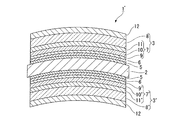
図1は、本発明の光学部品の第一の実施形態を模式的に示す側断面図であり、図1において符号1は眼鏡レンズ用の光学部品である。
この光学部品1は、プラスチック基材2と、プラスチック基材2の凸面上に配設された無機多層膜3とを備えて構成されている。プラスチック基材2の凸面と無機多層膜3との間には、本実施形態では機能性薄膜4が配設されている。この機能性薄膜4は、本実施形態ではプライマー層5とハードコート層6とからなっている。
(1) First Embodiment FIG. 1 is a side sectional view schematically showing a first embodiment of the optical component of the present invention. In FIG. 1, reference numeral 1 denotes an optical component for a spectacle lens.
The optical component 1 includes a
なお、以下の説明においては、プラスチック基材2の表面(凸面)に配設されている各膜3、4について主に説明するが、実際には、プラスチック基材2の裏面(凹面)にも、表面(凸面)に形成される各膜3、4と同等の膜が形成されている。
In the following description, the
プラスチック基材2は、例えば透明なプラスチックであるアクリル系樹脂、チオウレタン系樹脂、メタクリル系樹脂、アリル系樹脂、エピスルフィド系樹脂、ポリカーボネート系樹脂、ポリウレタン系樹脂、ポリエステル系樹脂、ポリスチレン系樹脂、エピスルフィド樹脂、ポリエ−テルサルホン樹脂ポリ4−メチルペンテン−1樹脂、ジエチレングリコールビスアリルカーボネート樹脂(CR−39)、ポリ塩化ビニル樹脂、ハロゲン含有共重合体、及びイオウ含有共重合体等によって形成されたものである。また、本実施形態では、プラスチック基材2の屈折率(nd)としては、例えば1.50、1.60、1.67、及び1.74のうちから選択されたものが用いられる。なお、プラスチック基材2の屈折率を1.6以上にする場合、プラスチック基材2としては、アリルカーボネート系樹脂、アクリレート系樹脂、メタクリレート系樹脂、及びチオウレタン系樹脂等を使用することが好ましい。
また、プラスチック基材2は透光性を有していれば透明でなくてもよく、着色されていてもよい。着色されたプラスチック基材2の透過率は、5〜85%であることが好ましい。
The
Moreover, the
機能性薄膜4は、前記したようにプラスチック基材2と無機多層膜3との間に配置されたもので、プラスチック基材2に接して配設されたプライマー層5と、このプライマー層5に接し、かつ無機多層膜3に接して配設されたハードコート層6とからなっている。
プライマー層5は、プラスチック基材2とハードコート層6との密着性を良好にするためのもので、密着層として機能するようになっている。また、光学部品1に対する衝撃を吸収するためのものでもあり、衝撃吸収層としても機能するようになっている。
The functional thin film 4 is disposed between the
The
このプライマー層5は、ポリウレタン系樹脂を主成分とするもので、本実施形態では、ポリウレタン系樹脂に例えば無機材料の微粒子を含有させたものである。なお、プライマー層5は、アクリル系樹脂、メタクリル系樹脂、及び有機珪素系樹脂の少なくとも一種を含んでいてもよい。プライマー層5の厚み(実際の厚み)については、0.5μm以上1.0μm以下程度とするのが好ましい。
The
このようなプライマー層5は、プライマー層5の形成材料液にプラスチック基材2を浸漬し、その後引き上げて乾燥することにより、プラスチック基材2上に所定の厚さで形成することができる。プライマー層5の形成材料液としては、例えば水又はアルコール系の溶媒に、前記したプライマー層5となる樹脂と無機酸化物微粒子ゾルとを分散又は溶解し、混合した液を用いることができる。
Such a
ハードコート層6は、プラスチック基材2を保護し、プラスチック基材2の損傷を抑制する機能を有するもので、耐擦傷性膜として機能するようになっている。
ハードコート層6は、例えばオルガノシロキサン系ハードコート層からなっている。オルガノシロキサン系ハードコート層は、オルガノシロキサン系樹脂に無機酸化物の微粒子を分散させたものである。無機酸化物としては、例えばルチル型の酸化チタンや、ケイ素、錫、ジルコニウム、及びアンチモンの酸化物が好適に用いられる。また、ハードコート層6として、例えば特公平4−55615号公報に開示されているような、コロイド状シリカ含有の有機ケイ素系樹脂であってもよい。ハードコート層6の厚み(実際の厚み)については、2μm以上4μm以下程度とするのが好ましい。
The
The
ハードコート層6は、ハードコート層6の形成材料液に、プライマー層5を形成したプラスチック基材2を浸漬し、その後引き上げて乾燥することにより、プラスチック基材2上のプライマー層5上に所定の厚さで形成することができる。ハードコート層6の形成材料液としては、例えば水又はアルコール系の溶媒に、前記したハードコート層6となる樹脂と無機酸化物微粒子ゾルとを分散又は溶解し、混合した液を用いることができる。
The
これらプライマー層5及びハードコート層6を含む機能性薄膜4については、その屈折率と、プラスチック基材2の屈折率とがほぼ同じであれば、機能性薄膜4とプラスチック基材2との界面での反射で生じる干渉縞の発生及び透過率の低下を抑制することができる。したがって、プラスチック基材2の屈折率に応じて、機能性薄膜4の屈折率を調整するのが望ましい。機能性薄膜4(プライマー層5、ハードコート層6)の屈折率の調整については、機能性薄膜4の主成分となる樹脂の種類(物性)を選択すること、あるいは、その主成分となる樹脂に添加する微粒子の種類(物性)を選択すること等によって行うことができる。
As for the functional thin film 4 including the
なお、本実施形態においては、機能性薄膜4がプライマー層5及びハードコート層6を含んで形成されているが、例えばプライマー層5とハードコート層6とのうち、いずれか一方、あるいは両方が省略されていてもよい。また、機能性薄膜4の構成膜として、例えばITO(Indium Tin Oxide)などからなる誘電体膜や金属膜を、前記プライマー層5及びハードコート層6に加えて配設してもよい。
また、本実施形態において、無機多層膜を構成する高屈折率無機材料と低屈折率無機材料との間に、厚さ20nm以下の誘電体膜又は金属膜を配設してもよい。なお、誘電体膜又は金属膜の厚さは、10nm以下であってもよい。
In the present embodiment, the functional thin film 4 is formed including the
In the present embodiment, a dielectric film or a metal film having a thickness of 20 nm or less may be disposed between the high refractive index inorganic material and the low refractive index inorganic material constituting the inorganic multilayer film. Note that the thickness of the dielectric film or the metal film may be 10 nm or less.
無機多層膜3は、前記プラスチック基材2に、高屈折率無機材料と低屈折率無機材料とが交互に複数積層されてなる多層構造の高屈折率層7を有し、該高屈折率層7上に、この高屈折率層7より低い屈折率の低屈折率無機材料からなる低屈折率層8を有した複層構成のもので、入射した光の反射を防止する反射防止膜としての機能を有したものである。この無機多層膜3は、本実施形態では400〜500nmの波長範囲における平均反射率が2〜10%であるように設計されている。
かかる平均反射率の範囲にあれば、眼鏡レンズとして使用した場合、充分な防眩効果が得られ、かつ良好な視認性を維持することができる。該波長域における平均反射率を10%以上にした場合、かかる眼鏡をかけた者は、眼鏡レンズの特に凹面からの入射光による反射にわずらわしさを感じるようになる。前記平均反射率は3〜10%であることが好ましい。
また、本実施形態においては、多層膜として無機多層膜を用いているが、本発明の効果を損なわない限り、有機多層膜を用いてもよい。
The
When the average reflectance is within the range, when used as a spectacle lens, a sufficient antiglare effect can be obtained and good visibility can be maintained. When the average reflectance in the wavelength region is set to 10% or more, a person wearing such spectacles feels troublesome in reflection by incident light from the concave surface of the spectacle lens. The average reflectance is preferably 3 to 10%.
In this embodiment, an inorganic multilayer film is used as the multilayer film, but an organic multilayer film may be used as long as the effects of the present invention are not impaired.
更に、無機多層膜3は、580〜780nmの波長域において反射率を1.5%以下であるように設計されることが好ましい。このような設計により、防眩効果及び視認性に一層の効果を有する眼鏡レンズを得ることができる。
Furthermore, the
高屈折率層7は、本実施形態では、前記プラスチック基材2側に設けられた高屈折率無機材料よりなる第1層9と、該第1層9上に設けられた低屈折率無機材料よりなる第2層10と、該第2層10上に設けられた高屈折率無機材料よりなる第3層11と、からなっている。
In the present embodiment, the high
第1層9は、ハードコート層6に接して設けられたもので、屈折率が2.0の二酸化ジルコニウム(ZrO2)からなっている。なお、第1層9を構成する高屈折率無機材料としては、ZrO2以外にも、例えば二酸化チタン(TiO2)や二酸化タンタル(Ta2O5)を用いることもできる。さらには、ジルコニウム、チタン、タンタルの複数種からなる合金の酸化物によって形成することもできる。また、これら以外にも、例えば酸化アルミニウム(Al2O3)、二酸化イットリウム(Y2O3)、二酸化ハフニウム(HfO2)、Nb2O5(二酸化ニオブ)を用いることもできる。
The
ここで、このように第1層9を高屈折率無機材料(ZrO2)で形成することにより、第1層9とハードコート層6との間の密着性を得ることができる。すなわち、高屈折率無機材料からなる層(ZrO2)とハードコート層6との密着性(密着力)のほうが、低屈折率無機材料からなる層(SiO2)とハードコート層6との密着性(密着力)よりも大きいためである。また、機能性薄膜4(プライマー層5、ハードコート層6)が省略された場合においても、高屈折率層(ZrO2)とプラスチック基材2との密着性(密着力)のほうが、低屈折率層(SiO2)とプラスチック基材2との密着性(密着力)よりも大きいため、密着性についてより有利になる。
Here, the adhesion between the
第2層10は、第1層9に接して設けられたもので、屈折率が1.47の二酸化珪素(SiO2)からなっている。なお、第2層10を構成する低屈折率無機材料としては、SiO2以外にも、例えば屈折率が1.36のMgF2を用いることができる。
The
第3層11は、第2層10に接して設けられたもので、第1層9と同様に二酸化ジルコニウム(ZrO2)からなっている。なお、この第3層11についても、第1層9と同様に、ZrO2以外の高屈折率無機材料によって形成することもできる。
また、高屈折率層7については、前記したように第1層9、第2層10、第3層11の三層構造で形成することなく、上述した反射率についての条件を満たせば、二層、あるいは四層以上で構成することもできる。
The
Further, the high
低屈折率層8は、前記第3層11に接して設けられたもので、前記第2層10と同様に二酸化珪素(SiO2)からなっている。
The low
また、本実施形態では、無機多層膜3の上、すなわち前記プラスチック基材2から最も遠い無機多層膜3の最外層(低屈折率層8)の上に、フッ素置換アルキル基含有有機ケイ素化合物を含む撥水撥油膜12が設けられている。
この撥水撥油膜12は、フッ素置換アルキル基含有有機ケイ素化合物を主成分とするもので、撥液性(撥水性、撥油性)を有するものである。すなわち、この撥水撥油膜12は、光学部品の表面エネルギーを低下させ、水やけ防止、汚れ防止の機能を発揮するとともに、光学部品表面のすべり性能を向上させ、その結果として、耐擦傷性を向上させることができる。
フッ素置換アルキル基含有有機ケイ素化合物としては、下記一般式(1):
In the present embodiment, the fluorine-substituted alkyl group-containing organosilicon compound is formed on the
The water /
As the fluorine-substituted alkyl group-containing organosilicon compound, the following general formula (1):

(式(1)中、Rfは炭素数1〜16の直鎖状又は分岐状パーフルオロアルキル基を表し、Yはヨウ素又は水素を表し、Y’は水素または炭素数1〜5の低級アルキル基を表し、Y”はフッ素又はトリフルオロメチル基を表し、R1は加水分解可能な基を表し、R2は水素又は不活性な一価の有機基を表し、a、b、c、dはそれぞれ0〜200の整数を表し、eは0又は1を表し、sおよびtはそれぞれ0〜2の整数を表し、wは1〜10の整数を表す。)
及び下記一般式(2)〜(5):
(In Formula (1), Rf represents a linear or branched perfluoroalkyl group having 1 to 16 carbon atoms, Y represents iodine or hydrogen, and Y ′ represents hydrogen or a lower alkyl group having 1 to 5 carbon atoms. Y ″ represents a fluorine or trifluoromethyl group, R 1 represents a hydrolyzable group, R 2 represents hydrogen or an inert monovalent organic group, a, b, c, d are Each represents an integer of 0 to 200, e represents 0 or 1, s and t each represents an integer of 0 to 2, and w represents an integer of 1 to 10.)
And the following general formulas (2) to (5):
(式(2)〜(5)中、Xは酸素又は二価の有機基を表し、X’は加水分解可能な基を表し、X”は二価の有機シリコーン基を表し、R3は炭素数1〜22の直鎖状又は分岐上アルキレン基を表し、qは1〜3の整数を表し、m、n、oはそれぞれ0〜200の整数を表し、pは1又は2を表し、rは2〜20の整数を表し、kは0〜2の整数を表し、zはkが0又は1である場合に0〜10の整数を表す。)
及び下記一般式(6):
(In the formulas (2) to (5), X represents oxygen or a divalent organic group, X ′ represents a hydrolyzable group, X ″ represents a divalent organic silicone group, and R 3 represents carbon. A linear or branched alkylene group of 1 to 22; q represents an integer of 1 to 3; m, n, and o each represents an integer of 0 to 200; p represents 1 or 2; Represents an integer of 2 to 20, k represents an integer of 0 to 2, and z represents an integer of 0 to 10 when k is 0 or 1.)
And the following general formula (6):
の中から選択される。
Selected from.
ここで、撥水撥油膜12に優れた耐久性を付与するには、一般式(1)〜(5)の中から選択されるフッ素置換アルキル基含有有機ケイ素化合物と、一般式(6)から選択されるフッ素置換アルキル基含有有機ケイ素化合物とを組み合わせて用いるのが好ましい。
一般式(1)〜(5)で示されるフッ素置換アルキル基含有有機ケイ素化合物としては、ダイキン工業株式会社製オプツール−DSX、オプツール−AES4などを用いることができる。また、一般式(6)示されるフッ素置換アルキル基含有有機ケイ素化合物としては、信越化学工業株式会社製KY−130、KY−164などを用いることができる。
Here, in order to impart excellent durability to the water /
As the fluorine-substituted alkyl group-containing organosilicon compound represented by the general formulas (1) to (5), OPTOOL-DSX, OPTOOL-AES4, etc. manufactured by Daikin Industries, Ltd. can be used. As the fluorine-substituted alkyl group-containing organosilicon compound represented by the general formula (6), KY-130, KY-164 manufactured by Shin-Etsu Chemical Co., Ltd. can be used.
(2) 第二の実施形態
図2は、本発明の光学部品の第二の実施形態を模式的に示す側断面図であり、図1において符号1’は眼鏡レンズ用の光学部品である。図2において、図1に示した光学部品1と同じ構成要素には、同一の符号を付して説明を省略する。
この光学部品1’は、第一の実施形態の光学部品1の構造に加えて、プラスチック基材2の凹面上に配設された無機多層膜3’を備えて構成されている。プラスチック基材2の凹面と無機多層膜3’との間には、本実施形態では機能性薄膜4が配設されている。この機能性薄膜4は、本実施形態ではプライマー層5とハードコート層6とからなっている。
(2) Second Embodiment FIG. 2 is a side sectional view schematically showing a second embodiment of the optical component of the present invention. In FIG. 1, reference numeral 1 ′ denotes an optical component for a spectacle lens. In FIG. 2, the same components as those of the optical component 1 shown in FIG.
This optical component 1 ′ includes an
無機多層膜3’は、前記プラスチック基材2に、高屈折率無機材料と低屈折率無機材料とが交互に複数積層されてなる多層構造の高屈折率層7’を有し、該高屈折率層7’上に、この高屈折率層7’より低い屈折率の低屈折率無機材料からなる低屈折率層8’を有した複層構成のものである。
The
高屈折率層7’は、本実施形態では、第一の実施形態と同様に、前記プラスチック基材2側に設けられた高屈折率無機材料よりなる第1層9’と、該第1層9’上に設けられた低屈折率無機材料よりなる第2層10’と、該第2層10’上に設けられた高屈折率無機材料よりなる第3層11’と、からなっている。
本実施形態における第1層9’、 第2層10’、 第3層11’に用いられる無機材料としては、第一の実施形態における第1層9、 第2層10、第3層11に用いられる無機材料と同様のものが挙げられる。
高屈折率層7’については、第一の実施形態における高屈折率層7と同様に、三層構造で形成することなく、二層、あるいは四層以上で構成することもできる。
In the present embodiment, the high
Inorganic materials used for the
The high
本実施形態において、無機多層膜3’は、第一の実施形態の無機多層膜3と同様に、400〜500nmの波長範囲における平均反射率が2〜10%であるように設計されてもよい。更に、無機多層膜3’は、580〜780nmの波長域において反射率を1.5%以下であるように設計されることが好ましい。プラスチック基材2の両面上に、かかる反射率の条件を満たす無機多層膜が配設されることにより、防眩効果及び視認性に一層の効果を有する眼鏡レンズを得ることができる。
In the present embodiment, the
また、本実施形態において、無機多層膜3’は、従来の反射防止膜と同様であってもよい。即ち、無機多層膜3’は、380〜780nmの波長範囲における平均反射率が1.5%以下の反射防止膜であってもよい。
In the present embodiment, the
さらに、本実施形態において、プラスチック基材2の凸面上に配設された無機多層膜3の400〜500nmの波長範囲における平均反射率は、プラスチック基材2の凹面上に配設された無機多層膜3’の400〜500nmの波長範囲における平均反射率よりも大きくしてもよい。プラスチック基材2の凸面上に配設された無機多層膜3は、400〜500nmの波長範囲における平均反射率が5〜10%であり、プラスチック基材2の凹面上に配設された無機多層膜3’は、400〜500nmの波長範囲における平均反射率が2〜4%であるように設計されることが好ましい。かかる反射率の条件を満たす無機多層膜が配設されることにより、防眩効果に一層の効果を有する眼鏡レンズを得ることができる。なお、プラスチック基材2の凹面上に配設された無機多層膜3’は、400〜500nmの波長範囲における平均反射率が3〜4%であってもよい。
Furthermore, in this embodiment, the average reflectance in the wavelength range of 400 to 500 nm of the
なお、本実施形態においては、機能性薄膜4がプライマー層5及びハードコート層6を含んで形成されているが、第一の実施形態と同様に、例えばプライマー層5とハードコート層6とのうち、いずれか一方、あるいは両方が省略されていてもよい。また、機能性薄膜4の構成膜として、例えばITO(Indium Tin Oxide)などからなる誘電体膜や金属膜を、前記プライマー層5及びハードコート層6に加えて配設してもよい。
また、本実施形態において、無機多層膜を構成する高屈折率無機材料と低屈折率無機材料との間に、厚さ20nm以下の誘電体膜又は金属膜を配設してもよい。なお、誘電体膜又は金属膜の厚さは、10nm以下であってもよい。
また、本実施形態においては、多層膜として無機多層膜を用いているが、本発明の効果を損なわない限り、有機多層膜を用いてもよい。
In the present embodiment, the functional thin film 4 is formed including the
In the present embodiment, a dielectric film or a metal film having a thickness of 20 nm or less may be disposed between the high refractive index inorganic material and the low refractive index inorganic material constituting the inorganic multilayer film. Note that the thickness of the dielectric film or the metal film may be 10 nm or less.
In this embodiment, an inorganic multilayer film is used as the multilayer film, but an organic multilayer film may be used as long as the effects of the present invention are not impaired.
次に、前記光学部品1の製造方法に基づき、本発明の光学部品の製造方法の一実施形態について説明する。
本実施形態の製造方法は、プラスチック基材2に対して従来と同様の方法で機能性薄膜4(プライマー層5、ハードコート層6)を形成する工程と、プラスチック基材2を加熱する工程と、加熱によってプラスチック基材2を所定温度(例えば70℃)に調整した後、このプラスチック基材2上に無機多層膜3を形成する工程と、無機多層膜3上に撥水撥油膜12を形成する工程と、を備えてなる。
Next, based on the manufacturing method of the said optical component 1, one Embodiment of the manufacturing method of the optical component of this invention is described.
The manufacturing method of the present embodiment includes a step of forming the functional thin film 4 (
無機多層膜3を形成する工程は、高屈折率無機材料と低屈折率無機材料とを交互に複数積層して多層構造の高屈折率層7を形成する処理と、この高屈折率層7上に、低屈折率無機材料からなる低屈折率層8を形成する処理と、を有している。これら各層の形成には、真空蒸着法が好適に用いられる。
The step of forming the
図3は、無機多層膜3の各層を形成するための蒸着装置30の一例を示す図である。図2に示すように蒸着装置30は、第1チャンバ31と第2チャンバ32と第3チャンバ33とを備えて構成されている。これら第1、第2、第3チャンバ31、32、33は、それぞれの内部がほぼ真空に減圧され、その状態に保持されるようになっている。また、蒸着装置30は、図示しない温調手段により、第1、第2、第3チャンバ31、32、33のそれぞれの内部温度が調整可能になっている。
FIG. 3 is a diagram illustrating an example of a
蒸着装置30は、第1、第2、第3チャンバ31、32、33のそれぞれの内部空間に、保持部材34を備えている。保持部材34は、その上面(保持面)が曲面状になっており、かつ、回転可能に構成されており、この上面上に複数のプラスチック基材2を保持するようになっている。
The
例えば、第1蒸着源35Aにビームを照射することにより、ZrO2の蒸気を第1蒸着源35Aから放出させ、保持部材34に保持されているプラスチック基材2上に供給し蒸着させる。これにより、無機多層膜3の高屈折率層7における第1層9と第3層11を形成することができる。同様に、第2蒸着源35Bにビームを照射することにより、SiO2の蒸気を第2蒸着源35Bから放出させ、保持部材34に保持されているプラスチック基材2上に供給し蒸着させる。これにより、無機多層膜3の高屈折率層7における第2層10と、低屈折率層8を形成することができる。
For example, by irradiating the first
すなわち、第1蒸着源35Aに対するビームの照射と第2蒸着源35Bに対するビームの照射とを交互に行うことにより、保持部材34に保持されているプラスチック基材2上に、高屈折率無機材料からなる層と低屈折率無機材料からなる層とを交互に形成し積層することができる。ただし、本発明では、無機多層膜3を400〜500nmの波長範囲における平均反射率が2〜10%であるように設計する。更に、無機多層膜3は、580〜780nmの波長域において反射率を1.5%以下であるように設計されることが好ましい。
なお、第1蒸着源35Aとして酸化ジルコニウム(ZrO)からなる蒸着源を用い、第2チャンバ32の内部空間に酸素を導入しながら第1蒸着源35Aにビームを照射し、二酸化ジルコニウム(ZrO2)からなる高屈折率無機材料層を形成するようにしてもよい。
That is, by alternately performing the beam irradiation on the first
Note that a vapor deposition source made of zirconium oxide (ZrO) is used as the first
このようにして無機多層膜3を形成したら、これの上に撥水撥油膜12を形成する。
撥水撥油膜12の形成方法としては、ディッピング法、スピンコート法、スプレー法などの湿式法、あるいは真空蒸着法などの乾式法がある。
湿式法の中では、ディッピング法が一般的であり、よく用いられる。この方法は、フッ素置換アルキル基含有有機ケイ素化合物を有機溶剤に溶解した液中に、無機多層膜3まで形成し光学部品を浸漬し、一定条件で引き上げ、乾燥させて成膜する方法である。有機溶剤としては、パーフルオロヘキサン、パーフルオロ−4−メトキシブタン、パーフルオロ−4−エトキシブタン、メタキシレンヘキサフルオライドなどが使用される。
When the
As a method for forming the water /
Among the wet methods, the dipping method is common and is often used. In this method, the
有機溶剤による希釈濃度は、0.01〜0.5重量%が好ましく、0.03〜0.1重量%がより好ましい。濃度が低すぎると十分な膜厚の撥水撥油層12が得られず、また、濃度が高すぎると塗布むらが発生しやすく、材料コストも高くなってしまう。
乾式法の中では、真空蒸着法がよく用いられる。この方法は、フッ素置換アルキル基含有有機ケイ素化合物を真空槽内で加熱して蒸発させ、撥水撥油膜12を形成する方法である。
The dilution concentration with an organic solvent is preferably 0.01 to 0.5% by weight, and more preferably 0.03 to 0.1% by weight. If the concentration is too low, the water /
Of the dry methods, vacuum deposition is often used. This method is a method of forming the water- and oil-
このようにして形成された光学部品1にあっては、無機多層膜3を400〜500nmの波長範囲における平均反射率が2〜10%であるように設計したので、前述したように反射特性及び視認性について、共に良好な性能を確保することができる。
また、光学部品の製造方法にあっては、このようなバランスのとれた優れた光学部品を確実に提供することができる。
In the optical component 1 formed as described above, the
Moreover, in the manufacturing method of an optical component, such a well-balanced and excellent optical component can be reliably provided.
以下、実施例により本発明をより具体的に説明するが、本発明は以下の実施例に限定されるものではない。 EXAMPLES Hereinafter, although an Example demonstrates this invention more concretely, this invention is not limited to a following example.
≪実験1≫
ウレタン系合成樹脂基板上に、屈折率1.67のシリコン系ハードコート、及び屈折率1.67のプライマーコートを加熱硬化にて施し、以下に示すように真空蒸着法により成膜した。
≪Experiment 1≫
A silicon hard coat having a refractive index of 1.67 and a primer coat having a refractive index of 1.67 were applied by heat curing on a urethane synthetic resin substrate, and a film was formed by vacuum deposition as described below.
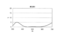
<実施例1>
凸面:レンズを真空槽内に設けられた回転するドームにセットし、真空槽内の温度を70度に加熱し、圧力が1.0×10⁻³Paになるまで排気し、加速電圧500V、加速電流100mAの条件でArイオンビームクリーニングを60秒間施した後、プラスチック基材側から順次、第1層ZrO2(屈折率2.00)を光学的膜厚0.035λ、第2層SiO2(屈折率1.47)を光学的膜厚0.565λ、第3層ZrO2(屈折率2.00)を光学的膜厚0.075λ、第4層SiO2(屈折率1.47)を光学的膜厚0.04λ、第5層ZrO2(屈折率2.00)を光学的膜厚0.32λ、第6層SiO2(屈折率1.47)を光学的膜厚0.26λで積層した。尚、λは設計の中心波長で500nmとした。
凹面:凸面と同様の装置、加工雰囲気、前処理後、プラスチック基材側から順次、第1層SiO2(屈折率1.47)を光学的膜厚0.10λ、第2層ZrO2(屈折率2.00)を光学的膜厚0.16λ、第3層SiO2(屈折率1.47)を光学的膜厚0.06λ、第4層ZrO2(屈折率2.00)を光学的膜厚0.25λ、第5層SiO2(屈折率1.47)を光学的膜厚0.28λで積層した。尚、λは設計の中心波長で500nmとした。
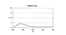
実施例1における分光特性を図1に示す。
<Example 1>
Convex surface: A lens is set on a rotating dome provided in a vacuum chamber, the temperature in the vacuum chamber is heated to 70 degrees, the pressure is exhausted until the pressure reaches 1.0 × 10 −3 Pa, an acceleration voltage of 500 V, After performing Ar ion beam cleaning for 60 seconds under the condition of an acceleration current of 100 mA, the first layer ZrO 2 (refractive index of 2.00) is sequentially formed from the plastic substrate side with an optical film thickness of 0.035λ and the second layer SiO 2. (Refractive index 1.47) with an optical film thickness of 0.565λ, third layer ZrO 2 (refractive index 2.00) with an optical film thickness 0.075λ, and fourth layer SiO 2 (refractive index 1.47). The optical film thickness is 0.04λ, the fifth layer ZrO 2 (refractive index 2.00) is the optical film thickness 0.32λ, and the sixth layer SiO 2 (refractive index 1.47) is the optical film thickness 0.26λ. Laminated. Note that λ is 500 nm as the design center wavelength.
Concave surface: device, processing atmosphere, pre-treatment similar to convex surface, first layer SiO 2 (refractive index 1.47) optical thickness 0.10λ, second layer ZrO 2 (refractive in order from plastic substrate side) The optical film thickness is 0.16λ, the third layer SiO 2 (refractive index 1.47) is the optical film thickness 0.06λ, and the fourth layer ZrO 2 (refractive index 2.00) is optical. A film thickness of 0.25λ and a fifth layer SiO 2 (refractive index of 1.47) were laminated with an optical film thickness of 0.28λ. Note that λ is 500 nm as the design center wavelength.
The spectral characteristics in Example 1 are shown in FIG.
<実施例2>
凸面:レンズを真空槽内に設けられた回転するドームにセットし、真空槽内の温度を70度に加熱し、圧力が1.0×10⁻³Paになるまで排気し、加速電圧500V、加速電流100mAの条件でArイオンビームクリーニングを60秒間施した後、プラスチック基材側から順次、第1層ZrO2(屈折率2.00)を光学的膜厚0.07λ、第2層SiO2(屈折率1.47)を光学的膜厚0.59λ、第3層ZrO2(屈折率2.00)を光学的膜厚0.06λ、第4層SiO2(屈折率1.47)を光学的膜厚0.04λ、第5層ZrO2(屈折率2.00)を光学的膜厚0.3λ、第6層SiO2(屈折率1.47)を光学的膜厚0.265λで積層した。尚、λは設計の中心波長で500nmとした。
凹面:凸面と同様の装置、加工雰囲気、前処理後、プラスチック基材側から順次、第1層SiO2(屈折率1.47)を光学的膜厚0.10λ、第2層ZrO2(屈折率2.00)を光学的膜厚0.16λ、第3層SiO2(屈折率1.47)を光学的膜厚0.06λ、第4層ZrO2(屈折率2.00)を光学的膜厚0.25λ、第5層SiO2(屈折率1.47)を光学的膜厚0.28λで積層した。尚、λは設計の中心波長で500nmとした。
実施例2における分光特性を図2に示す。
<Example 2>
Convex surface: A lens is set on a rotating dome provided in a vacuum chamber, the temperature in the vacuum chamber is heated to 70 degrees, the pressure is exhausted until the pressure reaches 1.0 × 10 −3 Pa, an acceleration voltage of 500 V, After Ar ion beam cleaning was performed for 60 seconds under the condition of an acceleration current of 100 mA, the first layer ZrO 2 (refractive index 2.00) was sequentially formed with an optical film thickness of 0.07λ and the second layer SiO 2 from the plastic substrate side. (Refractive index 1.47) with an optical thickness of 0.59λ, third layer ZrO 2 (refractive index 2.00) with an optical thickness of 0.06λ, and fourth layer SiO 2 (refractive index 1.47). The optical film thickness is 0.04λ, the fifth layer ZrO 2 (refractive index 2.00) is the optical film thickness 0.3λ, and the sixth layer SiO 2 (refractive index 1.47) is the optical film thickness 0.265λ. Laminated. Note that λ is 500 nm as the design center wavelength.
Concave surface: device, processing atmosphere, pre-treatment similar to convex surface, first layer SiO 2 (refractive index 1.47) optical thickness 0.10λ, second layer ZrO 2 (refractive in order from plastic substrate side) The optical film thickness is 0.16λ, the third layer SiO 2 (refractive index 1.47) is the optical film thickness 0.06λ, and the fourth layer ZrO 2 (refractive index 2.00) is optical. A film thickness of 0.25λ and a fifth layer SiO 2 (refractive index of 1.47) were laminated with an optical film thickness of 0.28λ. Note that λ is 500 nm as the design center wavelength.
The spectral characteristics in Example 2 are shown in FIG.
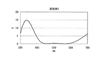
<実施例3>
凸面:レンズを真空槽内に設けられた回転するドームにセットし、真空槽内の温度を70度に加熱し、圧力が1.0×10⁻³Paになるまで排気し、加速電圧500V、加速電流100mAの条件でArイオンビームクリーニングを60秒間施した後、プラスチック基材側から順次、第1層ZrO2(屈折率2.00)を光学的膜厚0.095λ、第2層SiO2(屈折率1.47)を光学的膜厚0.595λ、第3層ZrO2(屈折率2.00)を光学的膜厚0.05λ、第4層SiO2(屈折率1.47)を光学的膜厚0.03λ、第5層ZrO2(屈折率2.00)を光学的膜厚0.305λ、第6層SiO2(屈折率1.47)を光学的膜厚0.275λで積層した。尚、λは設計の中心波長で500nmとした。
凹面:凸面と同様の装置、加工雰囲気、前処理後、プラスチック基材側から順次、第1層SiO2(屈折率1.47)を光学的膜厚0.10λ、第2層ZrO2(屈折率2.00)を光学的膜厚0.16λ、第3層SiO2(屈折率1.47)を光学的膜厚0.06λ、第4層ZrO2(屈折率2.00)を光学的膜厚0.25λ、第5層SiO2(屈折率1.47)を光学的膜厚0.28λで積層した。尚、λは設計の中心波長で500nmとした。
実施例3における分光特性を図3に示す。
<Example 3>
Convex surface: A lens is set on a rotating dome provided in a vacuum chamber, the temperature in the vacuum chamber is heated to 70 degrees, the pressure is exhausted until the pressure reaches 1.0 × 10 −3 Pa, an acceleration voltage of 500 V, After performing Ar ion beam cleaning for 60 seconds under the condition of an acceleration current of 100 mA, the first layer ZrO 2 (refractive index of 2.00) is sequentially formed from the plastic substrate side with an optical film thickness of 0.095λ and the second layer SiO 2. (Refractive index 1.47) with an optical thickness of 0.595λ, third layer ZrO 2 (refractive index 2.00) with an optical thickness of 0.05λ, and fourth layer SiO 2 (refractive index 1.47). The optical film thickness is 0.03λ, the fifth layer ZrO 2 (refractive index 2.00) is the optical film thickness 0.305λ, and the sixth layer SiO 2 (refractive index 1.47) is the optical film thickness 0.275λ. Laminated. Note that λ is 500 nm as the design center wavelength.
Concave surface: device, processing atmosphere, pre-treatment similar to convex surface, first layer SiO 2 (refractive index 1.47) optical thickness 0.10λ, second layer ZrO 2 (refractive in order from plastic substrate side) The optical film thickness is 0.16λ, the third layer SiO 2 (refractive index 1.47) is the optical film thickness 0.06λ, and the fourth layer ZrO 2 (refractive index 2.00) is optical. A film thickness of 0.25λ and a fifth layer SiO 2 (refractive index of 1.47) were laminated with an optical film thickness of 0.28λ. Note that λ is 500 nm as the design center wavelength.
The spectral characteristics in Example 3 are shown in FIG.
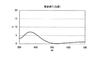
<比較例1>
凸面、凹面:レンズを真空槽内に設けられた回転するドームにセットし、真空槽内の温度を70度に加熱し、圧力が1.0×10⁻³Paになるまで排気し、加速電圧500V、加速電流100mAの条件でArイオンビームクリーニングを60秒間施した後、プラスチック基材側から順次、第1層SiO2(屈折率1.47)を光学的膜厚0.10λ、第2層ZrO2(屈折率2.00)を光学的膜厚0.16λ、第3層SiO2(屈折率1.47)を光学的膜厚0.06λ、第4層ZrO2(屈折率2.00)を光学的膜厚0.25λ、第5層SiO2(屈折率1.47)を光学的膜厚0.28λで積層した。尚、λは設計の中心波長で500nmとした。
比較例1における分光特性を図4に示す。
<Comparative Example 1>
Convex surface, concave surface: The lens is set in a rotating dome provided in the vacuum chamber, the temperature in the vacuum chamber is heated to 70 degrees, and the pressure is exhausted until the pressure becomes 1.0 × 10 −3 Pa, and the acceleration voltage After performing Ar ion beam cleaning for 60 seconds under conditions of 500 V and an acceleration current of 100 mA, the first layer SiO 2 (refractive index 1.47) is sequentially formed from the plastic substrate side with an optical film thickness of 0.10λ and the second layer. ZrO 2 (refractive index 2.00) has an optical film thickness of 0.16λ, the third layer SiO 2 (refractive index 1.47) has an optical film thickness of 0.06λ, and the fourth layer ZrO 2 (refractive index 2.00). ) Was laminated with an optical film thickness of 0.25λ, and a fifth layer SiO 2 (refractive index 1.47) was laminated with an optical film thickness of 0.28λ. Note that λ is 500 nm as the design center wavelength.
The spectral characteristics in Comparative Example 1 are shown in FIG.
実施例1〜3、比較例1における各成膜層の詳細を表1に示す。 Table 1 shows details of the respective film formation layers in Examples 1 to 3 and Comparative Example 1.
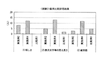
このようにして得られた光学物品の装用評価を行った。
(装用評価)
実施例に沿って作製した光学部品を装備した眼鏡を装用し、パソコンによるデスクワーク時に装用し、比較例に沿って作製した光学部品を装備した眼鏡との評価を行った。評価時の条件及び、判定項目は以下の通りである。
モニタ人数 :10名
ディスプレイ:17インチ液晶ディスプレイ
作業時間 :1時間/日
装用期間 :1週間
判定項目 :1.眩しさ 2.表示文字等の見え易さ 3.疲労感
実施例1〜3、比較例1の内、各評価項目に最も適していたものを○と評価した。結果を表2に示す。
Wear evaluation of the optical article thus obtained was performed.
(Wear evaluation)
The spectacles equipped with the optical parts produced according to the examples were worn and worn at the time of desk work by a personal computer, and the spectacles equipped with the optical parts produced according to the comparative examples were evaluated. Conditions at the time of evaluation and judgment items are as follows.
Number of monitors: 10 Display: 17-inch liquid crystal display Working time: 1 hour / day Wearing period: 1 week Judgment items: 1. 1.
このような装用比較評価を行った結果、400〜500nmの波長範囲で平均反射率を2〜10%とする特性が前記判定項目において効果があることが確認された。下記のように400〜500nmの波長範囲で平均反射率が約6%の実施例2が、各評価項目において最も適しているとされた。
実施例1〜3、比較例1の内、実施例2が、各評価項目に最も適していたと評価した人数
1.眩しさ :4/10名
2.表示の見え易さ :5/10名
3.疲労感 :6/10名
As a result of performing such wearing comparison evaluation, it was confirmed that the characteristic that the average reflectance is 2 to 10% in the wavelength range of 400 to 500 nm is effective in the determination item. As described below, Example 2 having an average reflectance of about 6% in the wavelength range of 400 to 500 nm was considered to be most suitable for each evaluation item.
Number of persons who evaluated that Example 2 was the most suitable for each evaluation item among Examples 1-3 and Comparative Example 1. Dazzle: 4/10 people Visibility of display: 5/10 people Fatigue: 6/10 people
≪実験2≫
合成樹脂基板上に、屈折率1.67のシリコン系ハードコートを加熱硬化にて施し、以下に示すように真空蒸着法により成膜した。
≪
On the synthetic resin substrate, a silicon hard coat having a refractive index of 1.67 was applied by heat curing, and a film was formed by vacuum deposition as shown below.
<実施例2>
≪実験1≫の実施例2と同様の成膜条件にて成膜を行った。
<Example 2>
Film formation was performed under the same film formation conditions as in Example 2 of << Experiment 1 >>.
<実施例4>
凸面:レンズを真空槽内に設けられた回転するドームにセットし、真空槽内の温度を70度に加熱し、圧力が1.0×10⁻³Paになるまで排気し、加速電圧500V、加速電流100mAの条件でArイオンビームクリーニングを60秒間施した後、プラスチック基材側から順次、第1層ZrO2(屈折率2.00)を光学的膜厚0.155λ、第2層SiO2(屈折率1.47)を光学的膜厚0.045λ、第3層ZrO2(屈折率2.00)を光学的膜厚0.5λ、第4層SiO2(屈折率1.47)を光学的膜厚0.335λで積層した。積層した。尚、λは設計の中心波長で500nmとした。
凹面:凸面と同様の装置、加工雰囲気、前処理後、プラスチック基材側から順次、第1層SiO2(屈折率1.47)を光学的膜厚0.10λ、第2層ZrO2(屈折率2.00)を光学的膜厚0.16λ、第3層SiO2(屈折率1.47)を光学的膜厚0.06λ、第4層ZrO2(屈折率2.00)を光学的膜厚0.25λ、第5層SiO2(屈折率1.47)を光学的膜厚0.28λで積層した。尚、λは設計の中心波長で500nmとした。
実施例4における分光特性を図5に示す。
<Example 4>
Convex surface: A lens is set on a rotating dome provided in a vacuum chamber, the temperature in the vacuum chamber is heated to 70 degrees, the pressure is exhausted until the pressure reaches 1.0 × 10 −3 Pa, an acceleration voltage of 500 V, After Ar ion beam cleaning was performed for 60 seconds under the condition of an acceleration current of 100 mA, the first layer ZrO 2 (refractive index 2.00) was sequentially formed from the plastic substrate side with an optical film thickness of 0.155λ and the second layer SiO 2. (Refractive index 1.47) with an optical thickness of 0.045λ, third layer ZrO 2 (refractive index 2.00) with an optical thickness of 0.5λ, and fourth layer SiO 2 (refractive index 1.47). Lamination was performed with an optical film thickness of 0.335λ. Laminated. Note that λ is 500 nm as the design center wavelength.
Concave surface: device, processing atmosphere, pre-treatment similar to convex surface, first layer SiO 2 (refractive index 1.47) optical thickness 0.10λ, second layer ZrO 2 (refractive in order from plastic substrate side) The optical film thickness is 0.16λ, the third layer SiO 2 (refractive index 1.47) is the optical film thickness 0.06λ, and the fourth layer ZrO 2 (refractive index 2.00) is optical. A film thickness of 0.25λ and a fifth layer SiO 2 (refractive index of 1.47) were laminated with an optical film thickness of 0.28λ. Note that λ is 500 nm as the design center wavelength.
The spectral characteristics in Example 4 are shown in FIG.
<比較例1>
≪実験1≫の比較例1と同様の成膜条件にて成膜を行った。
<Comparative Example 1>
Film formation was performed under the same film formation conditions as in Comparative Example 1 of << Experiment 1 >>.
実施例2、4、比較例1における各成膜層の詳細を表3に示す。 Table 3 shows details of the respective film formation layers in Examples 2 and 4 and Comparative Example 1.
このようにして得られた光学物品の装用評価を行った。
(装用評価)
実施例に沿って作製した光学部品を装備した眼鏡を装用し、パソコンによるデスクワーク時に装用し、比較例に沿って作製した光学部品を装備した眼鏡との評価を行った。評価時の条件及び、判定項目は以下の通りである。
モニタ人数 :20名
ディスプレイ:17インチ液晶ディスプレイ
作業時間 :1時間/日
装用期間 :1週間
判定項目 :1.眩しさ 2.表示文字等の見え易さ 3.疲労感
実施例2、4、比較例1の内、各評価項目に最も適していたものを○と評価した。○と評価したモニタ人数の合計を表4及び図6に示す。
Wear evaluation of the optical article thus obtained was performed.
(Wear evaluation)
The spectacles equipped with the optical parts produced according to the examples were worn and worn at the time of desk work by a personal computer, and the spectacles equipped with the optical parts produced according to the comparative examples were evaluated. Conditions at the time of evaluation and judgment items are as follows.
Number of monitors: 20 Display: 17-inch liquid crystal display Working time: 1 hour / day Wearing period: 1 week Judgment items: 1. 1.
このような装用比較評価を行った結果、400〜500nmの波長域において平均反射率を2〜10%とし、さらに580〜780nmの波長域において反射率を1.5%以下とすることにより、各判定においてより効果があることが確認された。 As a result of performing such wearing comparison evaluation, by setting the average reflectance to 2 to 10% in the wavelength range of 400 to 500 nm, and further setting the reflectance to 1.5% or less in the wavelength range of 580 to 780 nm, It was confirmed that the determination was more effective.
≪実験3≫
ウレタン系合成樹脂基板上に、屈折率1.67のシリコン系ハードコート、及び屈折率1.67のプライマーコートを加熱硬化にて施し、以下に示すように真空蒸着法により成膜した。
≪
A silicon hard coat having a refractive index of 1.67 and a primer coat having a refractive index of 1.67 were applied by heat curing on a urethane synthetic resin substrate, and a film was formed by vacuum deposition as described below.
<実施例5>
凸面、凹面:レンズを真空槽内に設けられた回転するドームにセットし、真空槽内の温度を70度に加熱し、圧力が1.0×10⁻³Paになるまで排気し、加速電圧500V、加速電流100mAの条件でArイオンビームクリーニングを60秒間施した後、プラスチック基材側から順次、第1層ZrO2(屈折率2.00)を光学的膜厚0.10λ、第2層SiO2(屈折率1.47)を光学的膜厚0.10λ、第3層ZrO2(屈折率2.00)を光学的膜厚0.205λ、第4層SiO2(屈折率1.47)を光学的膜厚0.06λ、第5層ZrO2(屈折率2.00)を光学的膜厚0.16λ、第6層SiO2(屈折率1.47)を光学的膜厚0.335λで積層した。尚、λは設計の中心波長で500nmとした。
実施例5における分光特性を図10に示す。
<Example 5>
Convex surface, concave surface: The lens is set in a rotating dome provided in the vacuum chamber, the temperature in the vacuum chamber is heated to 70 degrees, and the pressure is exhausted until the pressure reaches 1.0 × 10 −3 Pa, and the acceleration voltage After performing Ar ion beam cleaning for 60 seconds under the conditions of 500 V and acceleration current of 100 mA, the first layer ZrO 2 (refractive index of 2.00) is sequentially formed from the plastic substrate side with an optical film thickness of 0.10λ and the second layer. SiO 2 (refractive index 1.47) has an optical film thickness of 0.10λ, the third layer ZrO 2 (refractive index 2.00) has an optical film thickness of 0.205λ, and the fourth layer SiO 2 (refractive index 1.47). ) Optical film thickness 0.06λ, the fifth layer ZrO 2 (refractive index 2.00) is optical film thickness 0.16λ, and the sixth layer SiO 2 (refractive index 1.47) is
The spectral characteristics in Example 5 are shown in FIG.
<実施例6>
凸面:レンズを真空槽内に設けられた回転するドームにセットし、真空槽内の温度を70度に加熱し、圧力が1.0×10⁻³Paになるまで排気し、加速電圧500V、加速電流100mAの条件でArイオンビームクリーニングを60秒間施した後、プラスチック基材側から順次、第1層ZrO2(屈折率2.00)を光学的膜厚0.125λ、第2層SiO2(屈折率1.47)を光学的膜厚0.095λ、第3層ZrO2(屈折率2.00)を光学的膜厚0.21λ、第4層SiO2(屈折率1.47)を光学的膜厚0.07λ、第5層ZrO2(屈折率2.00)を光学的膜厚0.14λ、第6層SiO2(屈折率1.47)を光学的膜厚0.35λで積層した。尚、λは設計の中心波長で500nmとした。
凹面:凸面と同様の装置、加工雰囲気、前処理後、プラスチック基材側から順次、第1層ZrO2(屈折率2.00)を光学的膜厚0.105λ、第2層SiO2(屈折率1.47)を光学的膜厚0.095λ、第3層ZrO2(屈折率2.00)を光学的膜厚0.23λ、第4層SiO2(屈折率1.47)を光学的膜厚0.07λ、第5層ZrO2(屈折率2.00)を光学的膜厚0.14λ、第6層SiO2(屈折率1.47)を光学的膜厚0.33λで積層した。尚、λは設計の中心波長で500nmとした。
実施例6における凸面の分光特性を図11に示し、凹面の分光特性を図12に示す。
<Example 6>
Convex surface: A lens is set on a rotating dome provided in a vacuum chamber, the temperature in the vacuum chamber is heated to 70 degrees, the pressure is exhausted until the pressure reaches 1.0 × 10 −3 Pa, an acceleration voltage of 500 V, After performing Ar ion beam cleaning for 60 seconds under the condition of an acceleration current of 100 mA, the first layer ZrO 2 (refractive index of 2.00) is sequentially formed from the plastic substrate side with an optical film thickness of 0.125λ and the second layer SiO 2. (Refractive index 1.47) with an optical thickness of 0.095λ, third layer ZrO 2 (refractive index 2.00) with an optical thickness of 0.21λ, and fourth layer SiO 2 (refractive index 1.47). The optical film thickness is 0.07λ, the fifth layer ZrO 2 (refractive index 2.00) is the optical film thickness 0.14λ, and the sixth layer SiO 2 (refractive index 1.47) is the optical film thickness 0.35λ. Laminated. Note that λ is 500 nm as the design center wavelength.
Concave surface: Equipment similar to the convex surface, processing atmosphere, after pretreatment, and sequentially from the plastic substrate side, the first layer ZrO 2 (refractive index 2.00) has an optical film thickness of 0.105λ and the second layer SiO 2 (refractive The refractive index 1.47) is the optical film thickness 0.095λ, the third layer ZrO 2 (refractive index 2.00) is the optical film thickness 0.23λ, and the fourth layer SiO 2 (refractive index 1.47) is optical. The film thickness was 0.07λ, the fifth layer ZrO 2 (refractive index 2.00) was laminated with an optical film thickness 0.14λ, and the sixth layer SiO 2 (refractive index 1.47) was laminated with an optical film thickness 0.33λ. . Note that λ is 500 nm as the design center wavelength.
FIG. 11 shows the spectral characteristics of the convex surface in Example 6, and FIG. 12 shows the spectral characteristics of the concave surface.
<実施例7>
凸面:レンズを真空槽内に設けられた回転するドームにセットし、真空槽内の温度を70度に加熱し、圧力が1.0×10⁻³Paになるまで排気し、加速電圧500V、加速電流100mAの条件でArイオンビームクリーニングを60秒間施した後、プラスチック基材側から順次、第1層ZrO2(屈折率2.00)を光学的膜厚0.135λ、第2層SiO2(屈折率1.47)を光学的膜厚0.085λ、第3層ZrO2(屈折率2.00)を光学的膜厚0.20λ、第4層SiO2(屈折率1.47)を光学的膜厚0.055λ、第5層ZrO2(屈折率2.00)を光学的膜厚0.19λ、第6層SiO2(屈折率1.47)を光学的膜厚0.35λで積層した。尚、λは設計の中心波長で500nmとした。
凹面:凸面と同様の装置、加工雰囲気、前処理後、プラスチック基材側から順次、第1層ZrO2(屈折率2.00)を光学的膜厚0.11λ、第2層SiO2(屈折率1.47)を光学的膜厚0.09λ、第3層ZrO2(屈折率2.00)を光学的膜厚0.22λ、第4層SiO2(屈折率1.47)を光学的膜厚0.06λ、第5層ZrO2(屈折率2.00)を光学的膜厚0.20λ、第6層SiO2(屈折率1.47)を光学的膜厚0.33λで積層した。尚、λは設計の中心波長で500nmとした。
実施例7における凸面の分光特性を図13に示し、凹面の分光特性を図14に示す。
<Example 7>
Convex surface: A lens is set on a rotating dome provided in a vacuum chamber, the temperature in the vacuum chamber is heated to 70 degrees, the pressure is exhausted until the pressure reaches 1.0 × 10 −3 Pa, an acceleration voltage of 500 V, After performing Ar ion beam cleaning for 60 seconds under the condition of an acceleration current of 100 mA, the first layer ZrO 2 (refractive index of 2.00) is sequentially formed from the plastic substrate side with an optical film thickness of 0.135λ and the second layer SiO 2. (Refractive index 1.47) with an optical thickness of 0.085λ, third layer ZrO 2 (refractive index 2.00) with an optical thickness of 0.20λ, and fourth layer SiO 2 (refractive index 1.47). The optical film thickness is 0.055λ, the fifth layer ZrO 2 (refractive index 2.00) is the optical film thickness 0.19λ, and the sixth layer SiO 2 (refractive index 1.47) is the optical film thickness 0.35λ. Laminated. Note that λ is 500 nm as the design center wavelength.
Concave surface: device, processing atmosphere, pre-treatment similar to convex surface, first layer ZrO 2 (refractive index 2.00) with optical film thickness of 0.11λ and second layer SiO 2 (refractive in order from the plastic substrate side) The optical thickness is 0.09λ, the third layer ZrO 2 (refractive index 2.00) is optical thickness 0.22λ, and the fourth layer SiO 2 (refractive index 1.47) is optical. The film thickness was 0.06λ, the fifth layer ZrO 2 (refractive index 2.00) was laminated with an optical film thickness of 0.20λ, and the sixth layer SiO 2 (refractive index 1.47) was laminated with an optical film thickness of 0.33λ. . Note that λ is 500 nm as the design center wavelength.
FIG. 13 shows the spectral characteristics of the convex surface in Example 7, and FIG. 14 shows the spectral characteristics of the concave surface.
実施例5〜7における各成膜層の詳細を表5に示す。 Table 5 shows details of each film formation layer in Examples 5 to 7.
このようにして得られた光学物品の装用評価を行った。
(装用評価)
実施例に沿って作製した光学部品を装備した眼鏡を、パソコンによるデスクワーク時に装用し評価を行った。評価時の条件及び、判定項目は以下の通りである。
モニタ人数 :20名
ディスプレイ:17インチ液晶ディスプレイ
作業時間 :1時間/日
装用期間 :2週間
判定項目 :1.眩しさ 2.表示文字等の見え易さ 3.疲労感
実施例5〜7の内、各評価項目に最も適していたものを○と評価した。○と評価したモニタ人数の合計を表6及び図15に示す。
Wear evaluation of the optical article thus obtained was performed.
(Wear evaluation)
The spectacles equipped with the optical components produced according to the examples were worn at the time of desk work with a personal computer and evaluated. Conditions at the time of evaluation and judgment items are as follows.
Number of monitors: 20 Display: 17-inch liquid crystal display Working time: 1 hour / day Wearing period: 2 weeks Judgment items: 1. 1.
このような装用比較評価を行った結果、400〜500nmの波長域において凸面の平均反射率を5〜10%、凹面の平均反射率を2〜4%とし、580〜780nmの波長域において反射率を1.5%以下とすることにより、特に眩しさ低減において効果があることが確認された。 As a result of such comparative wearing evaluation, the average reflectance of the convex surface is 5 to 10% in the wavelength region of 400 to 500 nm, the average reflectance of the concave surface is 2 to 4%, and the reflectance is in the wavelength region of 580 to 780 nm. It was confirmed that by setting the ratio to 1.5% or less, it is particularly effective in reducing glare.
以上の結果から、本発明によれば、防眩効果を有し、装用による疲労感も無く、かつ、視認性が良好な光学部品及びその製造方法を提供できることが明らかである。 From the above results, it is apparent that the present invention can provide an optical component having an antiglare effect, no fatigue due to wearing, and good visibility, and a method for producing the same.
1、1’…光学部品、2…プラスチック基材、3、3’…無機多層膜、4…機能性薄膜、5…プライマー層(機能性薄膜)、6…ハードコート層(機能性薄膜)、7、7’…高屈折率層、8、8’…低屈折率層、9、9’…第1層、10、10’…第2層、11、11’…第3層、12…撥水撥油膜
DESCRIPTION OF SYMBOLS 1, 1 '... Optical component, 2 ...
Claims (18)
前記多層膜は、400〜500nmの波長範囲における平均反射率が2〜10%であることを特徴とする光学部品。 An optical component comprising a plastic substrate and a multilayer film disposed on at least the convex surface of both surfaces consisting of a convex surface and a concave surface of the plastic substrate,
The multilayer film has an average reflectance of 2 to 10% in a wavelength range of 400 to 500 nm.
及び下記一般式(2)〜(5):
及び下記一般式(6):
の中から選択される1種類以上のフッ素置換アルキル基含有有機ケイ素化合物である請求項7に記載の光学部品。 The fluorine-substituted alkyl group-containing organosilicon compound has the following general formula (1):
And the following general formulas (2) to (5):
And the following general formula (6):
The optical component according to claim 7, which is one or more fluorine-substituted alkyl group-containing organosilicon compounds selected from the group consisting of:
前記プラスチック基材を加熱する工程と、前記加熱によって前記プラスチック基材を所定温度に調整した後、前記プラスチック基材上に前記多層膜を形成する工程を備え、
前記多層膜を形成する工程は、高屈折率材料と低屈折率材料とを交互に複数積層し多層構造の高屈折率層を形成する処理と、前記高屈折率層上に、この高屈折率層より低い屈折率の低屈折率材料からなる低屈折率層を形成する処理と、を有するとともに、
前記多層膜の400〜500nmの波長範囲における平均反射率を2〜10%にすることを特徴とする請求項1〜13のいずれかの一項に記載の光学部品の製造方法。 A method for producing an optical component comprising: a plastic substrate; and a multilayer film disposed on at least the convex surface of both surfaces including the convex surface and the concave surface of the plastic substrate,
The step of heating the plastic substrate, and the step of forming the multilayer film on the plastic substrate after adjusting the plastic substrate to a predetermined temperature by the heating,
The step of forming the multilayer film includes a process of alternately stacking a plurality of high refractive index materials and low refractive index materials to form a high refractive index layer having a multilayer structure, and the high refractive index layer on the high refractive index layer. Forming a low refractive index layer made of a low refractive index material having a lower refractive index than the layer, and
The method of manufacturing an optical component according to any one of claims 1 to 13, wherein an average reflectance of the multilayer film in a wavelength range of 400 to 500 nm is set to 2 to 10%.
Priority Applications (7)
| Application Number | Priority Date | Filing Date | Title |
|---|---|---|---|
| JP2010288319A JP2012093689A (en) | 2010-09-29 | 2010-12-24 | Optical component and manufacturing method thereof |
| CN201180053968.5A CN103282823B (en) | 2010-09-29 | 2011-09-13 | Optical component and method for producing same |
| EP11828778.8A EP2624044B1 (en) | 2010-09-29 | 2011-09-13 | Optical component and method for producing same |
| KR1020137009773A KR101477940B1 (en) | 2010-09-29 | 2011-09-13 | Optical component and method for producing same |
| CA2812742A CA2812742C (en) | 2010-09-29 | 2011-09-13 | Optical component and method of manufacturing the same |
| PCT/JP2011/070856 WO2012043218A1 (en) | 2010-09-29 | 2011-09-13 | Optical component and method for producing same |
| US13/851,679 US10371867B2 (en) | 2010-09-29 | 2013-03-27 | Optical component and method of manufacturing the same |
Applications Claiming Priority (3)
| Application Number | Priority Date | Filing Date | Title |
|---|---|---|---|
| JP2010218711 | 2010-09-29 | ||
| JP2010218711 | 2010-09-29 | ||
| JP2010288319A JP2012093689A (en) | 2010-09-29 | 2010-12-24 | Optical component and manufacturing method thereof |
Related Child Applications (2)
| Application Number | Title | Priority Date | Filing Date |
|---|---|---|---|
| JP2012200993A Division JP5173076B2 (en) | 2010-09-29 | 2012-09-12 | Optical component and manufacturing method thereof |
| JP2013026090A Division JP5625077B2 (en) | 2010-09-29 | 2013-02-13 | Eyeglass lens and manufacturing method thereof |
Publications (2)
| Publication Number | Publication Date |
|---|---|
| JP2012093689A true JP2012093689A (en) | 2012-05-17 |
| JP2012093689A5 JP2012093689A5 (en) | 2012-11-01 |
Family
ID=45892689
Family Applications (1)
| Application Number | Title | Priority Date | Filing Date |
|---|---|---|---|
| JP2010288319A Pending JP2012093689A (en) | 2010-09-29 | 2010-12-24 | Optical component and manufacturing method thereof |
Country Status (7)
| Country | Link |
|---|---|
| US (1) | US10371867B2 (en) |
| EP (1) | EP2624044B1 (en) |
| JP (1) | JP2012093689A (en) |
| KR (1) | KR101477940B1 (en) |
| CN (1) | CN103282823B (en) |
| CA (1) | CA2812742C (en) |
| WO (1) | WO2012043218A1 (en) |
Cited By (21)
| Publication number | Priority date | Publication date | Assignee | Title |
|---|---|---|---|---|
| JP2014038247A (en) * | 2012-08-17 | 2014-02-27 | Nikon-Essilor Co Ltd | Ophthalmic lens |
| JP2014052394A (en) * | 2012-09-04 | 2014-03-20 | Cheil Industries Inc | Resin film and production method of resin film |
| WO2014050930A1 (en) * | 2012-09-28 | 2014-04-03 | 株式会社ニコン・エシロール | Optical component and method for producing same |
| WO2014069250A1 (en) * | 2012-11-05 | 2014-05-08 | 株式会社ニコン・エシロール | Optical component, method for producing optical component, and method for quantitatively determining ghost light |
| JP2014089353A (en) * | 2012-10-30 | 2014-05-15 | Jin Co Ltd | Transmitted beam observation apparatus |
| JP2014199327A (en) * | 2013-03-29 | 2014-10-23 | Hoya株式会社 | Spectacle lens |
| WO2015030246A1 (en) | 2013-08-30 | 2015-03-05 | Hoya株式会社 | Spectacle lens |
| WO2015030245A1 (en) | 2013-08-30 | 2015-03-05 | Hoya株式会社 | Spectacle lens and method for producing same |
| WO2015046540A1 (en) | 2013-09-30 | 2015-04-02 | ホヤ レンズ タイランド リミテッド | Transparent plastic substrate and plastic lens |
| WO2015122278A1 (en) * | 2014-02-13 | 2015-08-20 | 東海光学株式会社 | Optical product, glasses lens and glasses |
| JP2015203856A (en) * | 2014-04-16 | 2015-11-16 | 東海光学株式会社 | Optical product and spectacle lens |
| JP2016042178A (en) * | 2014-08-15 | 2016-03-31 | ワンレンソリューション オプティカル テクノロジー エスディーエヌ ビーエイチディーOnelensolution optical technology Sdn Bhd | Optical lens manufacturing method and optical lens |
| CN105759333A (en) * | 2014-12-30 | 2016-07-13 | 埃西勒国际通用光学公司 | Ophthalmic Anti-somnolence Lens, Device And Method |
| JP2016173612A (en) * | 2016-07-07 | 2016-09-29 | Hoya株式会社 | Spectacle lens |
| JPWO2015137282A1 (en) * | 2014-03-14 | 2017-04-06 | ホヤ レンズ タイランド リミテッドHOYA Lens Thailand Ltd | Mirror coat lens |
| JP2018503129A (en) * | 2015-01-07 | 2018-02-01 | ローデンシュトック ゲーエムベーハー | Layer system and optical element comprising the layer system |
| WO2019009127A1 (en) * | 2017-07-03 | 2019-01-10 | 東海光学株式会社 | Optical plastic product, and plastic spectacle lenses and spectacles |
| US10690944B2 (en) | 2014-12-01 | 2020-06-23 | Hoya Lens Thailand Ltd. | Spectacle lens that reflects blue light, and spectacles equipped with the spectacle lens |
| JP2020533618A (en) * | 2017-09-11 | 2020-11-19 | クアンタム イノベーションズ,インク. | High-energy visible light absorber materials and coating methods for ophthalmic substrates |
| KR20210104705A (en) | 2018-12-17 | 2021-08-25 | 가부시끼가이샤 도꾸야마 | Compositions for optical materials and optical materials |
| US11402666B2 (en) | 2014-10-17 | 2022-08-02 | Hoya Lens Thailand Ltd. | Spectacle lens and spectacles |
Families Citing this family (38)
| Publication number | Priority date | Publication date | Assignee | Title |
|---|---|---|---|---|
| AU2013261571B2 (en) * | 2012-05-16 | 2016-12-22 | Essilor International | Ophthalmic lens |
| JP5811228B2 (en) | 2013-06-24 | 2015-11-11 | 大日本印刷株式会社 | Image processing apparatus, display apparatus, image processing method, and image processing program |
| JP6253009B2 (en) | 2013-08-28 | 2017-12-27 | 東海光学株式会社 | Optical products and eyeglass lenses |
| US9946047B2 (en) * | 2014-03-04 | 2018-04-17 | Largan Precision Co., Ltd. | Annual optical spacer, image lens system, and mobile terminal |
| JP5685337B1 (en) * | 2014-05-02 | 2015-03-18 | 山田医療照明株式会社 | LIGHTING DEVICE AND LIGHTING DEVICE MANUFACTURING METHOD |
| US9057887B1 (en) * | 2014-05-06 | 2015-06-16 | Blue Light Eye Protection, Inc. | Materials and methods for mitigating the harmful effects of blue light |
| CN105445820A (en) * | 2014-08-21 | 2016-03-30 | 宸鸿科技(厦门)有限公司 | Optical film assembly |
| JPWO2016047523A1 (en) * | 2014-09-26 | 2017-07-13 | 旭硝子株式会社 | Optical element and imaging apparatus |
| US10459248B2 (en) | 2014-12-30 | 2019-10-29 | Essilor International | UV curable coating compositions for improved abrasion resistance |
| CN115712161A (en) | 2015-03-09 | 2023-02-24 | 视觉缓解公司 | Antistatic and antireflective coatings |
| CN107533154B (en) * | 2015-03-18 | 2022-07-01 | 视觉缓解公司 | Anti-cracking coating and method |
| KR102018287B1 (en) * | 2015-09-11 | 2019-09-05 | 주식회사 엘지화학 | Anti-reflective filmand display device |
| MX2018003759A (en) | 2015-09-29 | 2018-07-06 | Vision Ease Lp | Uv and high energy visible absorbing ophthalmic lenses. |
| EP3151041B1 (en) * | 2015-10-02 | 2019-02-20 | Tokai Optical Co., Ltd. | An optical film and spectacle lens |
| KR102478479B1 (en) * | 2015-10-05 | 2022-12-19 | 토카이 옵티칼 주식회사 | Optical product and eyeglass lens |
| MX2018004437A (en) | 2015-10-13 | 2018-05-28 | Vision Ease Lp | Optical filter with selective transmittance and reflectance. |
| CN106680905A (en) * | 2015-11-05 | 2017-05-17 | 大金工业株式会社 | Article with surface treatment layer |
| KR102487824B1 (en) | 2015-12-16 | 2023-01-12 | 미래나노텍(주) | Complex protective film |
| EP3505997A4 (en) * | 2016-08-22 | 2020-04-01 | Hoya Lens Thailand Ltd. | Spectacle lens and spectacles |
| CN108300303A (en) * | 2016-09-28 | 2018-07-20 | 卢火青 | The hydrophobic dust-proof nano coating composition and its preparation method and application of high-transmission rate |
| JP6368445B1 (en) * | 2017-03-27 | 2018-08-01 | 株式会社きもと | Laminated light shielding film, and light shielding ring, lens unit and camera module for optical equipment using the same |
| JP6473281B1 (en) | 2017-09-29 | 2019-02-20 | ホヤ レンズ タイランド リミテッドHOYA Lens Thailand Ltd | Eyeglass lenses and eyeglasses |
| CN109891304B (en) * | 2017-09-29 | 2021-12-07 | 豪雅镜片泰国有限公司 | Spectacle lens and spectacles |
| JP7265983B2 (en) | 2017-11-24 | 2023-04-27 | ホヤ レンズ タイランド リミテッド | spectacle lenses and spectacles |
| US11585962B2 (en) * | 2018-10-19 | 2023-02-21 | Racing Optics, Inc. | Transparent covering having anti-reflective coatings |
| US11583389B2 (en) | 2019-04-05 | 2023-02-21 | Amo Groningen B.V. | Systems and methods for correcting photic phenomenon from an intraocular lens and using refractive index writing |
| US11529230B2 (en) | 2019-04-05 | 2022-12-20 | Amo Groningen B.V. | Systems and methods for correcting power of an intraocular lens using refractive index writing |
| US11564839B2 (en) | 2019-04-05 | 2023-01-31 | Amo Groningen B.V. | Systems and methods for vergence matching of an intraocular lens with refractive index writing |
| US11944574B2 (en) | 2019-04-05 | 2024-04-02 | Amo Groningen B.V. | Systems and methods for multiple layer intraocular lens and using refractive index writing |
| US11678975B2 (en) | 2019-04-05 | 2023-06-20 | Amo Groningen B.V. | Systems and methods for treating ocular disease with an intraocular lens and refractive index writing |
| US11583388B2 (en) | 2019-04-05 | 2023-02-21 | Amo Groningen B.V. | Systems and methods for spectacle independence using refractive index writing with an intraocular lens |
| US11548356B2 (en) | 2020-03-10 | 2023-01-10 | Racing Optics, Inc. | Protective barrier for safety glazing |
| KR20220008695A (en) | 2020-07-30 | 2022-01-21 | 주식회사 케미그라스 | Lens to block ultraviolet rays perfectly |
| KR102588528B1 (en) | 2021-02-17 | 2023-10-11 | 서창민 | Infrared blocking composition for spectacle lenses, and spectacle lenses manufactured therefrom |
| US11490667B1 (en) | 2021-06-08 | 2022-11-08 | Racing Optics, Inc. | Low haze UV blocking removable lens stack |
| US11709296B2 (en) | 2021-07-27 | 2023-07-25 | Racing Optics, Inc. | Low reflectance removable lens stack |
| US11933943B2 (en) | 2022-06-06 | 2024-03-19 | Laminated Film Llc | Stack of sterile peelable lenses with low creep |
| US11808952B1 (en) | 2022-09-26 | 2023-11-07 | Racing Optics, Inc. | Low static optical removable lens stack |
Citations (12)
| Publication number | Priority date | Publication date | Assignee | Title |
|---|---|---|---|---|
| JPH03102301A (en) * | 1989-09-18 | 1991-04-26 | Kuraray Co Ltd | Method for evaluating characteristic of antireflection film and method for designing this film |
| JPH03116101A (en) | 1989-09-29 | 1991-05-17 | Kuraray Co Ltd | Antireflection film of optical articles made of synthetic resin |
| JP2001290112A (en) * | 2000-04-07 | 2001-10-19 | Hoya Corp | Mirror coated lens made of plastic |
| JP2002296405A (en) * | 2001-03-29 | 2002-10-09 | Sumitomo Chem Co Ltd | Antireflection base material with few reflection interference color and its color shading |
| JP2002296406A (en) * | 2001-03-29 | 2002-10-09 | Sumitomo Chem Co Ltd | Antireflection base material with few reflection interference color |
| JP2003105218A (en) * | 2001-09-28 | 2003-04-09 | Mitsui Chemicals Inc | Azaporphyrin-based dye and use thereof |
| JP2003215302A (en) * | 2002-01-21 | 2003-07-30 | Nikon-Essilor Co Ltd | Colored plastic lens and method for producing the same |
| WO2007077641A1 (en) * | 2005-12-28 | 2007-07-12 | Tokai Optical Co., Ltd. | Spectacle lens and spectacles |
| WO2008053712A1 (en) * | 2006-10-31 | 2008-05-08 | Nikon-Essilor Co., Ltd. | Eyeglass lens and method for production thereof |
| JP2009251008A (en) * | 2008-04-01 | 2009-10-29 | Seiko Epson Corp | Optical product and method for producing the same |
| WO2010016242A1 (en) * | 2008-08-04 | 2010-02-11 | 株式会社ニコン・エシロール | Optical component and optical component manufacturing method |
| JP2010511205A (en) * | 2006-11-28 | 2010-04-08 | ハイ・パフォーマンス・オプティクス・インコーポレーテッド | High-performance selective optical wavelength filtering provides improved contrast sensitivity |
Family Cites Families (28)
| Publication number | Priority date | Publication date | Assignee | Title |
|---|---|---|---|---|
| EP0112418B1 (en) | 1982-12-22 | 1987-03-11 | International Business Machines Corporation | Improved anti-reflection coating for visual display screens |
| JPS6310640A (en) | 1986-06-30 | 1988-01-18 | Hoya Corp | Coating composition for plastic lens |
| US4921760A (en) | 1986-09-26 | 1990-05-01 | Minolta Camera Kabushiki Kaisha | Anti-reflection coating of optical part made of synthetic resin |
| JPS6381402A (en) | 1986-09-26 | 1988-04-12 | Minolta Camera Co Ltd | Reflection reducing coating of plastic optical parts |
| JP2503732B2 (en) | 1990-06-21 | 1996-06-05 | トヨタ自動車株式会社 | Burner combustion control method |
| US6250758B1 (en) | 1997-05-16 | 2001-06-26 | Hoya Corporation | Plastic optical devices having antireflection film and mechanism for equalizing thickness of antireflection film |
| JP3975242B2 (en) | 1997-05-16 | 2007-09-12 | Hoya株式会社 | Plastic optical component with antireflection film |
| US8403478B2 (en) * | 2001-11-02 | 2013-03-26 | High Performance Optics, Inc. | Ophthalmic lens to preserve macular integrity |
| CN2478138Y (en) * | 2001-04-27 | 2002-02-20 | 厦门立扬光学科技有限公司 | Anti-electric antibiotic health lens |
| JP2003121604A (en) | 2001-10-12 | 2003-04-23 | Konica Corp | Optical lens part |
| JP4014840B2 (en) | 2001-10-12 | 2007-11-28 | 株式会社日立製作所 | Coma aberration correcting element and optical system for optical head using the same |
| JP2005011417A (en) | 2003-06-18 | 2005-01-13 | Samsung Yokohama Research Institute Co Ltd | Optical pickup device and optical information recording/reproducing device equipped with the same |
| JP2005215038A (en) * | 2004-01-27 | 2005-08-11 | Seiko Epson Corp | Spectacle lens |
| JP2006126233A (en) * | 2004-10-26 | 2006-05-18 | Seiko Epson Corp | Spectacle lens with antireflection film |
| JP2006251760A (en) | 2005-02-08 | 2006-09-21 | Seiko Epson Corp | Optical component and method for manufacturing the same |
| JP5211289B2 (en) | 2005-11-01 | 2013-06-12 | 東海光学株式会社 | Visible plastic lens |
| CN100495123C (en) * | 2005-12-30 | 2009-06-03 | 上海三联(集团)有限公司茂昌眼镜公司 | Ultrahard antifouling resin eyeglass and method for making same |
| JP2007183411A (en) * | 2006-01-06 | 2007-07-19 | Pentax Corp | Optical member having wavelength selectivity |
| US20070216861A1 (en) | 2006-03-20 | 2007-09-20 | Andrew Ishak | Ophthalmic system combining ophthalmic components with blue light wavelength blocking and color-balancing functionalities |
| US7520608B2 (en) * | 2006-03-20 | 2009-04-21 | High Performance Optics, Inc. | Color balanced ophthalmic system with selective light inhibition |
| CN101595421A (en) * | 2006-11-28 | 2009-12-02 | 高性能光学公司 | The high performance selective light wavelength filtering of improved contrast sensitivity is provided |
| JP2008152069A (en) | 2006-12-19 | 2008-07-03 | Nippon Electric Glass Co Ltd | Antireflection film |
| US8318245B2 (en) * | 2007-02-23 | 2012-11-27 | Essilor International (Compagnie Generale D'optique) | Method for producing an optical article coated with an antireflection or a reflective coating having improved adhesion and abrasion resistance properties |
| JP5066967B2 (en) | 2007-03-23 | 2012-11-07 | セイコーエプソン株式会社 | Method for manufacturing optical article |
| JP5044356B2 (en) | 2007-10-12 | 2012-10-10 | 日東光学株式会社 | Zoom lens system |
| JP2010026183A (en) * | 2008-07-17 | 2010-02-04 | Hoya Corp | Plastic lens and manufacturing method thereof |
| JP2010148860A (en) | 2008-11-28 | 2010-07-08 | Panasonic Corp | Intraoral measuring instrument |
| CN101441330B (en) * | 2008-12-09 | 2010-12-08 | 温州医学院眼视光研究院 | Light-induction anti-soil anti-fogging self-cleaning resin glasses lens and preparing method thereof |
-
2010
- 2010-12-24 JP JP2010288319A patent/JP2012093689A/en active Pending
-
2011
- 2011-09-13 CA CA2812742A patent/CA2812742C/en active Active
- 2011-09-13 CN CN201180053968.5A patent/CN103282823B/en active Active
- 2011-09-13 WO PCT/JP2011/070856 patent/WO2012043218A1/en active Application Filing
- 2011-09-13 EP EP11828778.8A patent/EP2624044B1/en active Active
- 2011-09-13 KR KR1020137009773A patent/KR101477940B1/en active IP Right Grant
-
2013
- 2013-03-27 US US13/851,679 patent/US10371867B2/en active Active
Patent Citations (12)
| Publication number | Priority date | Publication date | Assignee | Title |
|---|---|---|---|---|
| JPH03102301A (en) * | 1989-09-18 | 1991-04-26 | Kuraray Co Ltd | Method for evaluating characteristic of antireflection film and method for designing this film |
| JPH03116101A (en) | 1989-09-29 | 1991-05-17 | Kuraray Co Ltd | Antireflection film of optical articles made of synthetic resin |
| JP2001290112A (en) * | 2000-04-07 | 2001-10-19 | Hoya Corp | Mirror coated lens made of plastic |
| JP2002296405A (en) * | 2001-03-29 | 2002-10-09 | Sumitomo Chem Co Ltd | Antireflection base material with few reflection interference color and its color shading |
| JP2002296406A (en) * | 2001-03-29 | 2002-10-09 | Sumitomo Chem Co Ltd | Antireflection base material with few reflection interference color |
| JP2003105218A (en) * | 2001-09-28 | 2003-04-09 | Mitsui Chemicals Inc | Azaporphyrin-based dye and use thereof |
| JP2003215302A (en) * | 2002-01-21 | 2003-07-30 | Nikon-Essilor Co Ltd | Colored plastic lens and method for producing the same |
| WO2007077641A1 (en) * | 2005-12-28 | 2007-07-12 | Tokai Optical Co., Ltd. | Spectacle lens and spectacles |
| WO2008053712A1 (en) * | 2006-10-31 | 2008-05-08 | Nikon-Essilor Co., Ltd. | Eyeglass lens and method for production thereof |
| JP2010511205A (en) * | 2006-11-28 | 2010-04-08 | ハイ・パフォーマンス・オプティクス・インコーポレーテッド | High-performance selective optical wavelength filtering provides improved contrast sensitivity |
| JP2009251008A (en) * | 2008-04-01 | 2009-10-29 | Seiko Epson Corp | Optical product and method for producing the same |
| WO2010016242A1 (en) * | 2008-08-04 | 2010-02-11 | 株式会社ニコン・エシロール | Optical component and optical component manufacturing method |
Cited By (53)
| Publication number | Priority date | Publication date | Assignee | Title |
|---|---|---|---|---|
| JP2014038247A (en) * | 2012-08-17 | 2014-02-27 | Nikon-Essilor Co Ltd | Ophthalmic lens |
| JP2014052394A (en) * | 2012-09-04 | 2014-03-20 | Cheil Industries Inc | Resin film and production method of resin film |
| EP2902817B1 (en) * | 2012-09-28 | 2020-11-18 | Nikon-Essilor Co., Ltd. | Optical component and method for producing same |
| KR101918886B1 (en) * | 2012-09-28 | 2018-11-14 | 가부시키가이샤 니콘. 에시로루 | Optical component and method for producing same |
| KR101781703B1 (en) * | 2012-09-28 | 2017-09-26 | 가부시키가이샤 니콘. 에시로루 | Optical component and method for producing same |
| JP2016197253A (en) * | 2012-09-28 | 2016-11-24 | 株式会社ニコン・エシロール | Spectacle lens and manufacturing method therefor |
| CN104903756A (en) * | 2012-09-28 | 2015-09-09 | 株式会社尼康依视路 | Optical component and method for producing same |
| EP2902817A1 (en) | 2012-09-28 | 2015-08-05 | Nikon-Essilor Co., Ltd. | Optical component and method for producing same |
| WO2014050930A1 (en) * | 2012-09-28 | 2014-04-03 | 株式会社ニコン・エシロール | Optical component and method for producing same |
| JPWO2014050930A1 (en) * | 2012-09-28 | 2016-08-22 | 株式会社ニコン・エシロール | Eyeglass lens and manufacturing method thereof |
| JP2014089353A (en) * | 2012-10-30 | 2014-05-15 | Jin Co Ltd | Transmitted beam observation apparatus |
| WO2014069250A1 (en) * | 2012-11-05 | 2014-05-08 | 株式会社ニコン・エシロール | Optical component, method for producing optical component, and method for quantitatively determining ghost light |
| JPWO2014069250A1 (en) * | 2012-11-05 | 2016-09-08 | 株式会社ニコン・エシロール | Eyeglass lens and method for manufacturing eyeglass lens |
| CN104838305A (en) * | 2012-11-05 | 2015-08-12 | 株式会社尼康依视路 | Optical component, method for producing optical component, and method for quantitatively determining ghost light |
| JP2014199327A (en) * | 2013-03-29 | 2014-10-23 | Hoya株式会社 | Spectacle lens |
| JP2015049339A (en) * | 2013-08-30 | 2015-03-16 | Hoya株式会社 | Spectacle lens |
| JP2015049338A (en) * | 2013-08-30 | 2015-03-16 | Hoya株式会社 | Spectacle lens and manufacturing method thereof |
| WO2015030246A1 (en) | 2013-08-30 | 2015-03-05 | Hoya株式会社 | Spectacle lens |
| WO2015030245A1 (en) | 2013-08-30 | 2015-03-05 | Hoya株式会社 | Spectacle lens and method for producing same |
| CN105683819A (en) * | 2013-08-30 | 2016-06-15 | Hoya株式会社 | Spectacle lens |
| KR20160068747A (en) | 2013-08-30 | 2016-06-15 | 호야 가부시키가이샤 | Spectacle lens and method for producing same |
| AU2014312743B2 (en) * | 2013-08-30 | 2017-07-20 | Hoya Corporation | Spectacle lens and method for producing same |
| AU2014312744B2 (en) * | 2013-08-30 | 2017-06-22 | Hoya Corporation | Spectacle lens |
| WO2015046540A1 (en) | 2013-09-30 | 2015-04-02 | ホヤ レンズ タイランド リミテッド | Transparent plastic substrate and plastic lens |
| KR20210049958A (en) | 2013-09-30 | 2021-05-06 | 호야 렌즈 타일랜드 리미티드 | Transparent plastic substrate and plastic lens |
| EP3483219A1 (en) | 2013-09-30 | 2019-05-15 | Hoya Lens Thailand Ltd. | Transparent plastic substrate and plastic lens |
| KR20200108920A (en) | 2013-09-30 | 2020-09-21 | 호야 렌즈 타일랜드 리미티드 | Transparent plastic substrate and plastic lens |
| US11001699B2 (en) | 2013-09-30 | 2021-05-11 | Hoya Lens Thailand Ltd. | Transparent plastic substrate and plastic lens |
| KR20210006503A (en) | 2013-09-30 | 2021-01-18 | 호야 렌즈 타일랜드 리미티드 | Transparent plastic substrate and plastic lens |
| KR20160065845A (en) | 2013-09-30 | 2016-06-09 | 호야 렌즈 타일랜드 리미티드 | Transparent plastic substrate and plastic lens |
| KR20200108919A (en) | 2013-09-30 | 2020-09-21 | 호야 렌즈 타일랜드 리미티드 | Transparent plastic substrate and plastic lens |
| US10745539B2 (en) | 2013-09-30 | 2020-08-18 | Hoya Lens Thailand Ltd. | Transparent plastic substrate and plastic lens |
| US10947365B2 (en) | 2013-09-30 | 2021-03-16 | Hoya Lens Thailand Ltd. | Transparent plastic substrate and plastic lens |
| EP3483220A1 (en) | 2013-09-30 | 2019-05-15 | Hoya Lens Thailand Ltd. | Transparent plastic substrate and plastic lens |
| WO2015122278A1 (en) * | 2014-02-13 | 2015-08-20 | 東海光学株式会社 | Optical product, glasses lens and glasses |
| JP2015152735A (en) * | 2014-02-13 | 2015-08-24 | 東海光学株式会社 | Optical product and spectacle lens, and spectacle |
| US10107941B2 (en) | 2014-02-13 | 2018-10-23 | Tokai Optical Co., Ltd. | Optical product, and spectacle lens and spectacles |
| JPWO2015137282A1 (en) * | 2014-03-14 | 2017-04-06 | ホヤ レンズ タイランド リミテッドHOYA Lens Thailand Ltd | Mirror coat lens |
| JP2015203856A (en) * | 2014-04-16 | 2015-11-16 | 東海光学株式会社 | Optical product and spectacle lens |
| JP2016042178A (en) * | 2014-08-15 | 2016-03-31 | ワンレンソリューション オプティカル テクノロジー エスディーエヌ ビーエイチディーOnelensolution optical technology Sdn Bhd | Optical lens manufacturing method and optical lens |
| US11402666B2 (en) | 2014-10-17 | 2022-08-02 | Hoya Lens Thailand Ltd. | Spectacle lens and spectacles |
| US10690944B2 (en) | 2014-12-01 | 2020-06-23 | Hoya Lens Thailand Ltd. | Spectacle lens that reflects blue light, and spectacles equipped with the spectacle lens |
| CN105759333A (en) * | 2014-12-30 | 2016-07-13 | 埃西勒国际通用光学公司 | Ophthalmic Anti-somnolence Lens, Device And Method |
| JP2018503129A (en) * | 2015-01-07 | 2018-02-01 | ローデンシュトック ゲーエムベーハー | Layer system and optical element comprising the layer system |
| JP2019207424A (en) * | 2015-01-07 | 2019-12-05 | ローデンシュトック ゲーエムベーハー | Layer system and optical element comprising layer system |
| US10459124B2 (en) | 2015-01-07 | 2019-10-29 | Rodenstock Gmbh | Layer system and optical element comprising a layer system |
| JP7021156B2 (en) | 2015-01-07 | 2022-02-16 | ローデンシュトック ゲーエムベーハー | Optical elements with layered systems and layered systems |
| JP2016173612A (en) * | 2016-07-07 | 2016-09-29 | Hoya株式会社 | Spectacle lens |
| JP2019015764A (en) * | 2017-07-03 | 2019-01-31 | 東海光学株式会社 | Plastic optical product, plastic spectacle lens and spectacles |
| WO2019009127A1 (en) * | 2017-07-03 | 2019-01-10 | 東海光学株式会社 | Optical plastic product, and plastic spectacle lenses and spectacles |
| US11709292B2 (en) | 2017-07-03 | 2023-07-25 | Tokai Optical Co., Ltd. | Optical plastic product, and plastic spectacle lens and spectacles |
| JP2020533618A (en) * | 2017-09-11 | 2020-11-19 | クアンタム イノベーションズ,インク. | High-energy visible light absorber materials and coating methods for ophthalmic substrates |
| KR20210104705A (en) | 2018-12-17 | 2021-08-25 | 가부시끼가이샤 도꾸야마 | Compositions for optical materials and optical materials |
Also Published As
| Publication number | Publication date |
|---|---|
| EP2624044A1 (en) | 2013-08-07 |
| KR20130085415A (en) | 2013-07-29 |
| CA2812742A1 (en) | 2012-04-05 |
| US10371867B2 (en) | 2019-08-06 |
| EP2624044A4 (en) | 2016-03-30 |
| CN103282823A (en) | 2013-09-04 |
| US20130222913A1 (en) | 2013-08-29 |
| CN103282823B (en) | 2014-12-31 |
| WO2012043218A1 (en) | 2012-04-05 |
| KR101477940B1 (en) | 2014-12-30 |
| EP2624044B1 (en) | 2020-04-22 |
| CA2812742C (en) | 2017-02-28 |
Similar Documents
| Publication | Publication Date | Title |
|---|---|---|
| JP5625077B2 (en) | Eyeglass lens and manufacturing method thereof | |
| WO2012043218A1 (en) | Optical component and method for producing same | |
| JP5795675B2 (en) | Optical component for spectacle lens and method for manufacturing optical component for spectacle lens | |
| JP5966011B2 (en) | Eyeglass lens and manufacturing method thereof | |
| JP6073355B2 (en) | Eyeglass lens and method for manufacturing eyeglass lens | |
| JP5248516B2 (en) | Optical component and method of manufacturing optical component | |
| JP6581653B2 (en) | Eyeglass lenses | |
| WO2014208412A1 (en) | Optical component | |
| WO2010016242A1 (en) | Optical component and optical component manufacturing method |
Legal Events
| Date | Code | Title | Description |
|---|---|---|---|
| A521 | Request for written amendment filed |
Free format text: JAPANESE INTERMEDIATE CODE: A523 Effective date: 20120912 |
|
| A621 | Written request for application examination |
Free format text: JAPANESE INTERMEDIATE CODE: A621 Effective date: 20120912 |
|
| A871 | Explanation of circumstances concerning accelerated examination |
Free format text: JAPANESE INTERMEDIATE CODE: A871 Effective date: 20120912 |
|
| A975 | Report on accelerated examination |
Free format text: JAPANESE INTERMEDIATE CODE: A971005 Effective date: 20121002 |
|
| A131 | Notification of reasons for refusal |
Free format text: JAPANESE INTERMEDIATE CODE: A131 Effective date: 20121009 |
|
| A521 | Request for written amendment filed |
Free format text: JAPANESE INTERMEDIATE CODE: A523 Effective date: 20121107 |
|
| A02 | Decision of refusal |
Free format text: JAPANESE INTERMEDIATE CODE: A02 Effective date: 20121127 |
|
| A521 | Request for written amendment filed |
Free format text: JAPANESE INTERMEDIATE CODE: A523 Effective date: 20130213 |
|
| A911 | Transfer to examiner for re-examination before appeal (zenchi) |
Free format text: JAPANESE INTERMEDIATE CODE: A911 Effective date: 20130221 |
|
| A912 | Re-examination (zenchi) completed and case transferred to appeal board |
Free format text: JAPANESE INTERMEDIATE CODE: A912 Effective date: 20130419 |
|
| A521 | Request for written amendment filed |
Free format text: JAPANESE INTERMEDIATE CODE: A821 Effective date: 20130702 |