JP2012054205A - Light emitting device - Google Patents

Light emitting device Download PDF

Info

Publication number
JP2012054205A
JP2012054205A JP2010197880A JP2010197880A JP2012054205A JP 2012054205 A JP2012054205 A JP 2012054205A JP 2010197880 A JP2010197880 A JP 2010197880A JP 2010197880 A JP2010197880 A JP 2010197880A JP 2012054205 A JP2012054205 A JP 2012054205A
Authority
JP
Japan
Prior art keywords
light
circuit board
pressing member
housing
emitting device
Prior art date
Legal status (The legal status is an assumption and is not a legal conclusion. Google has not performed a legal analysis and makes no representation as to the accuracy of the status listed.)
Granted
Application number
JP2010197880A
Other languages
Japanese (ja)
Other versions
JP5685866B2 (en
Inventor
Shinya Kondo
慎也 近藤
Masato Ono
正人 小野
Hiroshi Miyairi
洋 宮入
Current Assignee (The listed assignees may be inaccurate. Google has not performed a legal analysis and makes no representation or warranty as to the accuracy of the list.)
Nichia Corp
Original Assignee
Nichia Corp
Priority date (The priority date is an assumption and is not a legal conclusion. Google has not performed a legal analysis and makes no representation as to the accuracy of the date listed.)
Filing date
Publication date
Application filed by Nichia Corp filed Critical Nichia Corp
Priority to JP2010197880A priority Critical patent/JP5685866B2/en
Publication of JP2012054205A publication Critical patent/JP2012054205A/en
Application granted granted Critical
Publication of JP5685866B2 publication Critical patent/JP5685866B2/en
Expired - Fee Related legal-status Critical Current
Anticipated expiration legal-status Critical

Links

Images

Landscapes

  • Fastening Of Light Sources Or Lamp Holders (AREA)
  • Arrangement Of Elements, Cooling, Sealing, Or The Like Of Lighting Devices (AREA)
  • Led Device Packages (AREA)

Abstract

【課題】光源が実装される回路基板と放熱部材の密着性を高め、光源の放熱性に優れる発光装置を提供する。
【解決手段】本発明の発光装置(100)は、前方に開口し、下壁内面(31)と上壁内面(32)を有する筐体(30)と、前記下壁内面(31)上に設けられ、上面に光源(10)が実装された回路基板(20)と、前記上壁内面(32)と前記回路基板(20)の上面に挟持される押さえ付け部材(40)と、を備えることを特徴とする。
【選択図】図1
Provided is a light emitting device that enhances the adhesion between a circuit board on which a light source is mounted and a heat dissipation member, and is excellent in heat dissipation of the light source.
A light emitting device (100) according to the present invention has a housing (30) that opens forward and has a lower wall inner surface (31) and an upper wall inner surface (32), and the lower wall inner surface (31). A circuit board (20) provided with a light source (10) mounted on the upper surface, and a pressing member (40) clamped between the upper wall inner surface (32) and the upper surface of the circuit board (20). It is characterized by that.
[Selection] Figure 1

Description

本発明は、発光装置に関し、より詳細には光源の放熱性を高める発光装置の構造に関するものである。   The present invention relates to a light emitting device, and more particularly to a structure of a light emitting device that enhances heat dissipation of a light source.

近年、光源として発光ダイオード(Light Emitting Diode:LED)やレーザダイオード(LASER Diode:LD)等の半導体発光素子を搭載した発光装置が、各種の照明や表示装置に利用されている。特に、これら半導体発光素子は、消費電力が低く長寿命であるため、蛍光灯や白熱電球に代替可能な照明用光源として注目を集めている。   2. Description of the Related Art In recent years, light-emitting devices equipped with semiconductor light-emitting elements such as light-emitting diodes (LEDs) and laser diodes (LASER Diodes: LDs) as light sources have been used for various lighting and display devices. In particular, these semiconductor light-emitting elements have attracted attention as illumination light sources that can replace fluorescent lamps and incandescent bulbs because of their low power consumption and long life.

例えば特許文献1には、透光性部材からなるレンズとハウジングにより形成された気密空間内に、少なくともレンズと対向する面を反射面とするリフレクタと、該反射面の一部に光を照射するLEDと、を有するLEDフットライトが記載されており、このLEDフットライトにおいて、LEDが実装される基板は、リフレクタから延びた基板ガイドに沿って挟持されている。   For example, in Patent Document 1, light is applied to a part of the reflecting surface, a reflector having a reflecting surface at least on a surface facing the lens, in an airtight space formed by a lens made of a translucent member and a housing. An LED footlight having an LED is described. In the LED footlight, a substrate on which the LED is mounted is sandwiched along a substrate guide extending from a reflector.

また例えば特許文献2には、複数のLED素子が実装され、少なくとも一方の側面が連続的に傾斜した形状を有する実装基板と、該実装基板を収容する筐体と、を備え、該筐体は、該実装基板の一方の側面に対応する内側側面が該一方の側面の傾斜角度と同一角度で傾斜した形状を有するLED照明装置が記載されている。   Further, for example, Patent Document 2 includes a mounting substrate having a shape in which a plurality of LED elements are mounted and at least one side surface is continuously inclined, and a housing that houses the mounting substrate. The LED lighting device has a shape in which an inner side surface corresponding to one side surface of the mounting substrate is inclined at the same angle as the inclination angle of the one side surface.

特開2006−331988号公報JP 2006-331988 A 特開2010−135126号公報JP 2010-135126 A 特開2009−158354号公報JP 2009-158354 A 特開2010−170847号公報JP 2010-170847 A

しかしながら、上記特許文献1に記載されているような、リフレクタから延びた基板ガイドにLED実装基板を挟持する構造では、LED実装基板とハウジング等の放熱部材との接触面積が小さいため、LEDの放熱性が低いという問題がある。また、上記特許文献2に記載されたLED照明装置においては、実装基板側面と筐体内側側面を接触させても、ネジ止め等により実装基板に反りやうねりを生じると、実装基板裏面が筐体から浮いてしまい、LEDの放熱性が低下する虞がある。   However, in the structure in which the LED mounting substrate is sandwiched between the substrate guides extending from the reflector as described in Patent Document 1, the contact area between the LED mounting substrate and the heat radiating member such as the housing is small. There is a problem that the nature is low. Moreover, in the LED lighting device described in Patent Document 2, even if the mounting substrate side surface and the housing inner side surface are brought into contact with each other, if the mounting substrate is warped or swelled by screwing or the like, the mounting substrate back surface is There is a possibility that the heat dissipation of the LED is lowered.

そこで、本発明はかかる事情に鑑みてなされたものであり、光源が実装される回路基板と放熱部材の密着性を高め、光源の放熱性に優れる発光装置を提供することを目的とする。   Therefore, the present invention has been made in view of such circumstances, and an object of the present invention is to provide a light emitting device that improves the adhesion between a circuit board on which a light source is mounted and a heat radiating member, and is excellent in the heat radiating property of the light source.

上記課題を解決するために、本発明に係る発光装置は、前方に開口し、下壁内面と上壁内面を有する筐体と、前記下壁内面上に設けられ、上面に光源が実装された回路基板と、前記上壁内面と前記回路基板の上面に挟持される押さえ付け部材と、を備えることを特徴とする。   In order to solve the above problems, a light-emitting device according to the present invention has a housing that opens forward, has a lower wall inner surface and an upper wall inner surface, is provided on the lower wall inner surface, and a light source is mounted on the upper surface. A circuit board, and a pressing member held between the inner surface of the upper wall and the upper surface of the circuit board are provided.

本発明によれば、簡易な構成で且つ簡便に、光源が実装される回路基板と放熱部材の密着性を高め、光源の放熱性に優れる発光装置を提供することができる。   According to the present invention, it is possible to provide a light-emitting device that has a simple configuration and easily improves the adhesion between a circuit board on which a light source is mounted and a heat dissipation member, and is excellent in heat dissipation of the light source.

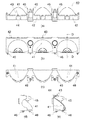
本発明の一実施の形態に係る発光装置の外観を示す概略斜視図(a)と、それを分解して各構成を示す概略斜視図(b)である。It is the schematic perspective view (a) which shows the external appearance of the light-emitting device which concerns on one embodiment of this invention, and the schematic perspective view (b) which decomposes | disassembles it and shows each structure. 本発明の一実施の形態に係る発光装置の内部の構成を示す概略正面図(a)と、そのA−A断面を拡大して示す概略断面図(b)である。It is the schematic front view (a) which shows the structure inside the light-emitting device which concerns on one embodiment of this invention, and the schematic sectional drawing (b) which expands and shows the AA cross section. 本発明の一実施の形態に係る発光装置の筐体を示す概略正面図(a)と、その一部Bを拡大して示す概略正面図(b)、及びC−C断面を拡大して示す概略断面図(c)である。BRIEF DESCRIPTION OF THE DRAWINGS The schematic front view (a) which shows the housing | casing of the light-emitting device which concerns on one embodiment of this invention, the schematic front view (b) which expands and shows a part B, and expands and shows CC cross section. It is a schematic sectional drawing (c). 本発明の一実施の形態に係る発光装置の押さえ付け部材を示す概略上面図(a)と、概略正面図(b)と、概略下面図(c)と、概略側面図(d)と、図3(b)のD−D断面を示す概略断面図(e)である。FIG. 1 is a schematic top view (a), a schematic front view (b), a schematic bottom view (c), a schematic side view (d), and a diagram showing a pressing member of a light emitting device according to an embodiment of the present invention. It is a schematic sectional drawing (e) which shows DD cross section of 3 (b).

以下、発明の実施の形態について適宜図面を参照して説明する。ただし、以下に説明する発光装置は、本発明の技術思想を具体化するためのものであって、本発明を以下のものに限定しない。特に、以下に記載されている構成要素の寸法、材質、形状、その相対的配置等は特定的な記載がない限りは、本発明の範囲をそれのみに限定する趣旨ではなく、単なる説明例にすぎない。なお、各図面が示す部材の大きさや位置関係等は、説明を明確にするため誇張していることがある。   Hereinafter, embodiments of the invention will be described with reference to the drawings as appropriate. However, the light emitting device described below is for embodying the technical idea of the present invention, and the present invention is not limited to the following. In particular, the dimensions, materials, shapes, relative arrangements, and the like of the constituent elements described below are not intended to limit the scope of the present invention only to specific examples unless otherwise specified. Only. In addition, the size, positional relationship, and the like of members illustrated in each drawing may be exaggerated for clarity of explanation.

<実施の形態1>
図1(a)は、実施の形態1に係る発光装置の外観を示す概略斜視図であって、図1(b)は、それを分解して各構成を示す概略斜視図である。図2(a)は、実施の形態1に係る発光装置の内部の構成を示す概略正面図であって、図2(b)は、そのA−A断面を拡大して示す概略断面図である。図1,2に示すように、実施の形態1の発光装置100は、主として、光源10と、この光源が上面に実装される回路基板20と、この回路基板上に設置される押さえ付け部材40と、これらを前方から挿入し内部に収容可能な筐体30と、この筐体を前方から密閉可能なカバー部材50と、により構成されている。なお以下、発光装置100の各方向は、この筐体30の前方から後方に向かう方向を「奥行き」方向、上下方向を「高さ」方向、この2つの方向に垂直な左右方向を「幅」方向として記述することがある。
<Embodiment 1>
FIG. 1A is a schematic perspective view showing an external appearance of the light emitting device according to Embodiment 1, and FIG. 1B is a schematic perspective view showing each component by disassembling it. 2A is a schematic front view showing an internal configuration of the light-emitting device according to Embodiment 1, and FIG. 2B is a schematic cross-sectional view showing an enlarged AA cross section. . As shown in FIGS. 1 and 2, the light-emitting device 100 according to the first embodiment mainly includes a light source 10, a circuit board 20 on which the light source is mounted, and a pressing member 40 installed on the circuit board. And a housing 30 that can be inserted from the front and accommodated therein, and a cover member 50 that can seal the housing from the front. Hereinafter, the directions of the light emitting device 100 are the “depth” direction as the direction from the front to the rear of the housing 30, the “height” direction as the up and down direction, and the “width” as the right and left direction perpendicular to these two directions. Sometimes described as a direction.

より詳細には、筐体30は、前方に開口し、上壁、下壁、左側壁、右側壁、背壁を有する、箱状の容器である。回路基板20は、筐体30と同様に幅方向に長尺で、筐体の下壁内面31上に1枚設けられており、幅方向に複数の光源10が一列に実装されている。押さえ付け部材40は、光源10からの光を前方に反射させる光反射体であって、回路基板20の上面と筐体の上壁内面32に挟持されている。カバー部材50は、筐体30に固定され、この筐体の前方の開口を密閉し、押さえ付け部材40を筐体内部に保持させている。   More specifically, the housing 30 is a box-shaped container that opens forward and has an upper wall, a lower wall, a left side wall, a right side wall, and a back wall. The circuit board 20 is long in the width direction like the case 30 and is provided on the inner surface 31 of the lower wall of the case, and a plurality of light sources 10 are mounted in a row in the width direction. The pressing member 40 is a light reflector that reflects light from the light source 10 forward, and is sandwiched between the upper surface of the circuit board 20 and the upper wall inner surface 32 of the housing. The cover member 50 is fixed to the housing 30, seals the opening in front of the housing, and holds the pressing member 40 inside the housing.

このような構成の発光装置100であれば、図2(b)に示すように、回路基板20上に押さえ付け部材40を組み付けて、その組付体を筐体30の後方に押し込むことにより、押さえ付け部材40がその弾性により撓んで上下方向の押圧力を生じ、回路基板20を筐体の下壁内面31に押さえ付けることができる。したがって、押さえ付け部材40の筐体30への挿入方向(取り付け方向)と回路基板20の押圧方向が交差する構造でありながら、少ない部品点数及び工数で回路基板20を効率良く押圧することができる。これにより、簡易な構成で且つ簡便に、回路基板20の下面(裏面)の広範な領域を筐体の下壁内面31に密着させやすく、光源10の放熱性を高めることができる。   If it is the light-emitting device 100 of such a structure, as shown in FIG.2 (b), by assembling the pressing member 40 on the circuit board 20, and pushing the assembly to the back of the housing | casing 30, The pressing member 40 is bent by its elasticity to generate a vertical pressing force, and the circuit board 20 can be pressed to the inner surface 31 of the lower wall of the casing. Therefore, the circuit board 20 can be efficiently pressed with a small number of parts and man-hours, while the insertion direction (attachment direction) of the pressing member 40 to the housing 30 and the pressing direction of the circuit board 20 intersect. . Thereby, it is easy to make the wide area | region of the lower surface (back surface) of the circuit board 20 contact | adhere to the lower wall inner surface 31 of a housing | casing easily with simple structure, and can improve the heat dissipation of the light source 10. FIG.

以下、実施の形態1の発光装置100の構造について詳述する。図3(a)は、実施の形態1に係る発光装置の筐体を示す概略正面図であって、図3(b)は、図3(a)の一部Bを拡大して示す概略正面図であり、図3(c)は、図3(a)のC−C断面を拡大して示す概略断面図である。図4は、実施の形態1に係る発光装置の押さえ付け部材を示す概略図であり、図3(a)は概略上面図、図3(b)は概略正面図、図3(c)は概略下面図、図3(d)は概略側面図、図3(e)は図3(b)のD−D断面を示す概略断面図である。   Hereinafter, the structure of the light emitting device 100 of Embodiment 1 will be described in detail. FIG. 3A is a schematic front view showing a housing of the light emitting device according to Embodiment 1, and FIG. 3B is a schematic front view showing a part B of FIG. FIG. 3C is a schematic cross-sectional view showing an enlarged CC cross section of FIG. 4 is a schematic view showing a pressing member of the light emitting device according to Embodiment 1, FIG. 3 (a) is a schematic top view, FIG. 3 (b) is a schematic front view, and FIG. 3 (c) is a schematic diagram. FIG. 3 (d) is a schematic side view, and FIG. 3 (e) is a schematic cross-sectional view showing a DD cross section of FIG. 3 (b).

図2,3に示すように、筐体30の下壁内面31及び上壁内面32は、筐体の後方にいくにつれて互いに近付いている。このような構成により、押さえ付け部材40が筐体30の後方に押し込まれていくほど上下方向の押圧力が大きくなり、回路基板20を下壁内面31に簡便に押さえ付けやすく、好ましい。このとき、筐体の下壁内面31及び上壁内面32は、両方が傾斜していてもよいし、いずれか一方が傾斜していてもよい。押さえ付け部材40に生じる押圧力により、回路基板20を下壁内面31に対して略垂直に効率良く押圧するためには、下壁内面31と上壁内面32のなす角度θ3(=θ1+θ2)は、0°より大きく20°以下であることが好ましい。なお、θ1,θ2は各々、下壁内面31,上壁内面32の基準面(水平面)からの筐体外側に開く方向の傾斜角度である。筐体30は、本例のように下壁、背壁、上壁を有するものが好ましいが、背壁を略有さずに下壁と上壁が略接しているものでもよい。 As shown in FIGS. 2 and 3, the lower wall inner surface 31 and the upper wall inner surface 32 of the housing 30 are closer to each other toward the rear of the housing. Such a configuration is preferable because the pressing force in the vertical direction increases as the pressing member 40 is pushed rearward of the housing 30, and the circuit board 20 is easily pressed against the inner surface 31 of the lower wall. At this time, both the lower wall inner surface 31 and the upper wall inner surface 32 of the housing may be inclined, or one of them may be inclined. In order to efficiently press the circuit board 20 substantially perpendicularly to the lower wall inner surface 31 by the pressing force generated in the pressing member 40, an angle θ 3 (= θ 1) between the lower wall inner surface 31 and the upper wall inner surface 32 is formed. + Θ 2 ) is preferably greater than 0 ° and 20 ° or less. In addition, θ 1 and θ 2 are inclination angles in a direction of opening outward from the reference surface (horizontal plane) of the lower wall inner surface 31 and the upper wall inner surface 32, respectively. The housing 30 preferably has a lower wall, a back wall, and an upper wall as in this example, but may have a structure in which the lower wall and the upper wall are substantially in contact with each other without substantially having a back wall.

図2,4に示すように、押さえ付け部材40の上面は、筐体の上壁内面32に当接する凸部43を有している。この凸部43は、押さえ付け部材40の上面に設けられる代わりに、筐体の上壁内面32に設けられてもよい。このように、筐体の上壁内面32と押さえ付け部材40の上面のいずれか一方が、その他方に当接する凸部を有することが好ましい。このような凸部が設けられることにより、押さえ付け部材40の回路基板20に対する押圧力の起点(力点)の場所、大きさ、数を選択することができ、回路基板面内の押圧力の分布を制御しやすい。   As shown in FIGS. 2 and 4, the upper surface of the pressing member 40 has a convex portion 43 that comes into contact with the upper wall inner surface 32 of the housing. This convex portion 43 may be provided on the inner surface 32 of the upper wall of the housing instead of being provided on the upper surface of the pressing member 40. Thus, it is preferable that either one of the upper wall inner surface 32 of the housing or the upper surface of the pressing member 40 has a convex portion that abuts on the other side. By providing such a convex portion, the location, size, and number of pressing force starting points (force points) of the pressing member 40 against the circuit board 20 can be selected, and the distribution of the pressing force within the circuit board surface is selected. Easy to control.

複数の光源10が回路基板20上に間隔dで配列される場合、その光源10の配列方向における、凸部43と筐体の上壁内面32(以下、凸部が筐体の上壁内面32に設けられる場合の凸部と押さえ付け部材40の上面の関係にも適用される)との接触幅wは、間隔dより小さいことが好ましい。特に、凸部43と筐体の上壁内面32の接触部は、点状であることが好ましい。これにより、押さえ付け部材40の回路基板20に対する押圧力の起点を局所的に設け、該凸部43から押圧力を略均等に拡散させ、回路基板20面内の押圧力の分布をより制御しやすくすることができる。なお、ここでいう「点状」とは、完全な点接触のみを意味するのではなく、微小な接触面積を有する場合も含む意味で用いる。このような構成は、凸部43の表面が曲面、例えば半球状や球面の一部又はそれが扁形された曲面で構成されることにより達成できる。このほか、凸部43は筐体の上壁内面32と線又は面で接触してもよく、略円柱面や、略平坦な上面を有する形状(断面視台形状など)でもよい。このような場合には、凸部43と筐体の上壁内面32の接触幅wは、間隔dに対して、例えば5%以上10%以下とすることが好ましい。凸部43の高さ(突出量)は、特に限定されないが、例えば1mm以上4mm以下程度である。また、凸部43が複数設けられる場合には、各凸部から略均等な押圧力を生じやすくするため、各凸部の高さが略等しいことが好ましい。   When the plurality of light sources 10 are arranged on the circuit board 20 with the interval d, the convex portion 43 and the upper wall inner surface 32 of the casing in the arrangement direction of the light sources 10 (hereinafter, the convex portion is the upper wall inner surface 32 of the casing). The contact width w between the convex portion and the upper surface of the pressing member 40 is preferably smaller than the distance d. In particular, the contact portion between the convex portion 43 and the upper wall inner surface 32 of the housing is preferably point-like. Thereby, the starting point of the pressing force of the pressing member 40 on the circuit board 20 is locally provided, the pressing force is diffused substantially uniformly from the convex portion 43, and the distribution of the pressing force in the surface of the circuit board 20 is further controlled. It can be made easier. The term “spot-like” as used herein does not mean only a complete point contact, but also includes a case having a minute contact area. Such a configuration can be achieved by forming the surface of the convex portion 43 with a curved surface, for example, a hemispherical shape, a part of a spherical surface, or a curved surface with a flat shape. In addition, the convex portion 43 may contact the upper wall inner surface 32 of the housing by a line or a surface, and may have a substantially cylindrical surface or a shape having a substantially flat upper surface (such as a trapezoidal shape in cross section). In such a case, the contact width w between the convex portion 43 and the upper wall inner surface 32 of the housing is preferably set to, for example, 5% or more and 10% or less with respect to the distance d. Although the height (projection amount) of the convex part 43 is not specifically limited, For example, it is about 1 mm or more and 4 mm or less. Further, when a plurality of convex portions 43 are provided, it is preferable that the heights of the respective convex portions are substantially equal in order to easily generate a substantially uniform pressing force from each convex portion.

凸部43の幅方向の位置は、光源10の略真上であることが好ましい。これにより、光源10を中心としてその周囲の回路基板20を下壁内面31に略均等に押し付けることができる。また、複数の光源10が回路基板20上に配列される場合、凸部43は、隣り合う2つの光源10間、特にその略中央に設けられてもよい。これにより、1つの凸部43によって、その凸部を挟む光源10近傍の回路基板面に対する押圧力を効率良く制御することができる。凸部43の奥行き方向の位置は、押さえ付け部材40の重心の奥行き方向の位置と略同じであることが好ましい。これにより、押さえ付け部材40の傾きを抑制し、押圧力を効率良く底面側に伝達することができる。また、凸部43から回路基板20の光源10の近傍に押圧力を効率良く伝達するために、光源と光源の間隔dは100mm以下であることが好ましく、装置上面視における光源10と凸部43との距離は50mm以下であることが好ましい。さらに、光源10近傍の回路基板面を効果的に押さえ付けるために、押さえ付け部材40の底面と光源10との最短距離は、10mm以下とすることが好ましい。   The position of the convex portion 43 in the width direction is preferably substantially directly above the light source 10. Thereby, the circuit board 20 around the light source 10 can be pressed almost uniformly against the inner surface 31 of the lower wall. Moreover, when the several light source 10 is arranged on the circuit board 20, the convex part 43 may be provided between the two adjacent light sources 10, especially the approximate center. Thereby, the pressing force against the circuit board surface in the vicinity of the light source 10 sandwiching the convex portion can be efficiently controlled by the single convex portion 43. The position of the convex portion 43 in the depth direction is preferably substantially the same as the position of the center of gravity of the pressing member 40 in the depth direction. Thereby, the inclination of the pressing member 40 can be suppressed and the pressing force can be efficiently transmitted to the bottom surface side. Further, in order to efficiently transmit the pressing force from the convex portion 43 to the vicinity of the light source 10 of the circuit board 20, the distance d between the light source and the light source is preferably 100 mm or less, and the light source 10 and the convex portion 43 in the top view of the apparatus. Is preferably 50 mm or less. Furthermore, in order to effectively press the circuit board surface near the light source 10, the shortest distance between the bottom surface of the pressing member 40 and the light source 10 is preferably 10 mm or less.

図2,4に示すように、押さえ付け部材40は、光源10の後方から該光源の上方及び左右側方を覆うように湾曲して設けられた光反射部41を有している。回路基板20は、熱源である光源10の近傍において特に発熱しやすいが、このように押さえ付け部材40が光源10を囲む光反射部41を有することにより、光反射部41の底面が光源10を取り囲むように回路基板面に接し、回路基板20の光源10の近傍を下壁内面31に強く押さえ付けて光源10の放熱性を高めやすい。また、光反射部41が奥行き方向に張り出して形成されることで、押さえ付け部材40の傾きを抑制することができる。複数の光源10が回路基板20上に配列される場合、光反射部41は各光源10に対応して設けられることが好ましい。   As shown in FIGS. 2 and 4, the pressing member 40 has a light reflecting portion 41 that is curved from behind the light source 10 so as to cover the upper side and the left and right sides of the light source. The circuit board 20 is likely to generate heat particularly in the vicinity of the light source 10 that is a heat source. However, since the pressing member 40 includes the light reflecting portion 41 surrounding the light source 10 in this manner, the bottom surface of the light reflecting portion 41 causes the light source 10 to be used. The circuit board surface is touched so as to be surrounded, and the vicinity of the light source 10 of the circuit board 20 is strongly pressed against the inner surface 31 of the lower wall, so that the heat dissipation of the light source 10 can be easily improved. In addition, since the light reflecting portion 41 is formed so as to protrude in the depth direction, the inclination of the pressing member 40 can be suppressed. When a plurality of light sources 10 are arranged on the circuit board 20, it is preferable that the light reflecting portion 41 is provided corresponding to each light source 10.

図2,4に示すように、押さえ付け部材40は、光反射部41の上位に、略平坦な上面を有する板状部42を有しており、凸部43は、この板状部42に設けられている。これにより、凸部43に生じる押圧力を板状部42に伝達させて広範に拡散させることができる。また、板状部42の一部には2つの切り欠きが設けられ、この切り欠きに挟まれる部位は弾性部44となっており、特に本例では、この弾性部44に凸部43が設けられている。このような弾性部44が形成されることにより、押さえ付け部材40の筐体20内への押し込みにより発生する押圧力を調整しやすく、また弾性部44の反作用により、上壁内面32を押し上げる力が生じ、押さえ付け部材40を筐体30内に強固に固定することができる。押さえ付け部材40が光反射部41を複数有する場合、板状部42は、複数の光反射部41の上位に跨って1つ設けられてもよいし、各光反射部41に対応して複数設けられてもよい。なお、この凸部43、弾性部44や切り欠きは、必須の要素ではなく省略することもできる。例えば、凸部が筐体の上壁内面32に設けられ、該凸部に当接する平坦な上面の弾性部44が押さえ付け部材40に設けられた構造でもよい。ここで、「弾性」とは、例えば樹脂材料であれば、曲げ弾性率(ISO規格178、JIS規格K7171)が2000MPa以上4000MPa以下程度であることが好ましく、さらにシャルピー衝撃強さ(ノッチ付き)(ISO規格179、JIS規格K7111)が10kJ/m2以上であることが好ましい。 As shown in FIGS. 2 and 4, the pressing member 40 has a plate-like portion 42 having a substantially flat upper surface above the light reflecting portion 41, and the convex portion 43 is formed on the plate-like portion 42. Is provided. Thereby, the pressing force generated in the convex portion 43 can be transmitted to the plate-like portion 42 and diffused widely. In addition, two cutouts are provided in a part of the plate-like portion 42, and a portion sandwiched between the cutouts is an elastic portion 44. In particular, in this example, a convex portion 43 is provided on the elastic portion 44. It has been. By forming such an elastic portion 44, it is easy to adjust the pressing force generated by pushing the pressing member 40 into the housing 20, and the force that pushes up the inner surface 32 of the upper wall by the reaction of the elastic portion 44. As a result, the pressing member 40 can be firmly fixed in the housing 30. When the pressing member 40 has a plurality of light reflecting portions 41, one plate-like portion 42 may be provided over the upper portions of the plurality of light reflecting portions 41, or a plurality of plate-like portions 42 corresponding to each light reflecting portion 41. It may be provided. The convex portion 43, the elastic portion 44, and the notch are not essential elements and can be omitted. For example, a structure in which the convex portion is provided on the inner surface 32 of the upper wall of the housing and the elastic portion 44 having a flat upper surface contacting the convex portion is provided in the pressing member 40 may be used. Here, “elasticity” is, for example, a resin material, preferably having a flexural modulus (ISO standard 178, JIS standard K7171) of about 2000 MPa to 4000 MPa, and further, Charpy impact strength (notched) ( The ISO standard 179 and the JIS standard K7111) are preferably 10 kJ / m 2 or more.

図2,4に示すように、押さえ付け部材40は、板状部41に連続して上下方向に立設された板状体の支柱部45を有している。この支柱部45は、「リブ」のように、板状部42を支えて補強する機能を有し、押さえ付け部材40の傾きを抑制して押圧力を底面側に効率良く伝達しやすくする。また、支柱部45は、その上面が凸部43の高さより低く且つ筐体の上壁内面32と同様に傾斜して、後方に延出しており、押さえ付け部材40を筐体30の後方に押し込む際のガイドとしての機能を有する。さらに、支柱部45は、押さえ付け部材40の位置(押し込み深さ)を規制するストッパーとしての機能を有し、押し込み過ぎによる凸部43や弾性部44の破損を防止することができる。また、押さえ付け部材40全体の押し込み深さを略均等にする、つまり装置上面視において押さえ付け部材40を筐体30の前面に対して略平行に設置でき、回路基板20全体を筐体の下壁内面31に略均等に押さえ付けられ、また押さえ付け部材40が光反射体である場合には光軸の傾きを抑制できる。支柱部45は、押さえ付け部材40全体の均衡を図り、押さえ付け部材40に略対称的に複数設けられることが好ましく、また光反射部41に並設されることが好ましい。例えば、支柱部45は、光反射部41が1つの場合はその両側に、光反射部41が複数の場合は少なくとも光反射部41間に設けられることが好ましく、本例のように光反射部41間に2つ設けられてもよい。   As shown in FIGS. 2 and 4, the pressing member 40 includes a plate-like column support 45 that is erected in the vertical direction continuously to the plate-like portion 41. This support portion 45 has a function of supporting and reinforcing the plate-like portion 42 like a “rib”, and suppresses the inclination of the pressing member 40 and facilitates efficient transmission of the pressing force to the bottom surface side. Further, the support column 45 has an upper surface lower than the height of the convex portion 43 and is inclined in the same manner as the upper wall inner surface 32 of the housing, and extends rearward. It functions as a guide when pushing in. Furthermore, the support | pillar part 45 has a function as a stopper which controls the position (pressing depth) of the pressing member 40, and can prevent the damage of the convex part 43 and the elastic part 44 by excessive pressing. Further, the pressing depth of the entire pressing member 40 can be made substantially equal, that is, the pressing member 40 can be installed substantially parallel to the front surface of the casing 30 when the apparatus is viewed from above, and the entire circuit board 20 can be placed under the casing. When the pressing member 40 is a light reflector, the inclination of the optical axis can be suppressed. In order to balance the entire pressing member 40, it is preferable that a plurality of support columns 45 be provided approximately symmetrically on the pressing member 40, and it is preferable that the supporting column 45 be provided in parallel with the light reflecting portion 41. For example, it is preferable that the support columns 45 are provided on both sides of the light reflecting portion 41 when there is one light reflecting portion 41, and at least between the light reflecting portions 41 when there are a plurality of light reflecting portions 41. Two may be provided between 41.

図2,3に示すように、筐体の下壁内面31は、凹凸面を有し、光源10は、この凹凸面の凸領域311上に配置されている。凹領域312上においては、回路基板20及び押さえ付け部材40の下壁内面31による支えがなくなるため、凸領域311上にある光反射部41の底面に押圧力が集中しやすくなり、回路基板20の光源10の周囲を効率良く下壁内面31に押さえ付けやすい。また、光源10が肉厚の大きい凸領域311上に配置されることで、光源10の放熱性を高めやすい。特に、図2,3,4に示すように、押さえ付け部材40の上面は、筐体の上壁内面32に当接する凸部43を有し、該凸部43は筐体の下壁内面31の凸領域311上に配置されている。このように、筐体の上壁内面32と押さえ付け部材40の上面のいずれか一方が、その他方に当接し且つ凹凸面の凸領域311上に配置された凸部を有することが好ましい。筐体の下壁内面の凸領域311上に凸部が配置されることで、押圧力を凸領域311上の回路基板20に効率良く伝達させ、回路基板20を凸領域311に押さえ付けやすい。   As shown in FIGS. 2 and 3, the lower wall inner surface 31 of the housing has an uneven surface, and the light source 10 is disposed on the convex region 311 of the uneven surface. On the concave region 312, since the support by the circuit board 20 and the lower wall inner surface 31 of the pressing member 40 is lost, the pressing force is easily concentrated on the bottom surface of the light reflecting portion 41 on the convex region 311. It is easy to efficiently press the periphery of the light source 10 against the inner surface 31 of the lower wall. Moreover, it is easy to improve the heat dissipation of the light source 10 by arrange | positioning the light source 10 on the convex area | region 311 with large thickness. In particular, as shown in FIGS. 2, 3, and 4, the upper surface of the pressing member 40 has a convex portion 43 that abuts the upper wall inner surface 32 of the casing, and the convex portion 43 is the lower wall inner surface 31 of the casing. It is arranged on the convex region 311. Thus, it is preferable that either one of the upper wall inner surface 32 of the housing or the upper surface of the pressing member 40 has a convex portion that is in contact with the other side and is disposed on the convex region 311 of the concave and convex surface. By arranging the convex portion on the convex region 311 on the inner surface of the lower wall of the housing, the pressing force can be efficiently transmitted to the circuit board 20 on the convex region 311, and the circuit board 20 can be easily pressed against the convex region 311.

図2,4に示すように、押さえ付け部材40は、底面の一部に回路基板20に係止する鉤部46を有することが好ましい。押さえ付け部材40は、この鉤部46が回路基板20に設けられた穴に係止されて仮留めされる。このような鉤部46により、押さえ付け部材40を光源10に対して精度良く設置し、回路基板20の各光源10の近傍を精度良く押さえ付けることができ、また押さえ付け部材40が光反射体である場合には優れた光学特性が得られる。特に、押さえ付け部材40は、筐体の下壁内面31の凹領域312上に配置される鉤部46を有することが好ましい。凹領域312上に鉤部46を有することで、押さえ付け部材40の浮きを抑制して、効率良く凸領域311に回路基板20を押さえ付けることができる。   As shown in FIGS. 2 and 4, it is preferable that the pressing member 40 has a flange portion 46 that is engaged with the circuit board 20 at a part of the bottom surface. The pressing member 40 is temporarily fastened by locking the flange 46 in a hole provided in the circuit board 20. With such a flange portion 46, the pressing member 40 can be installed with high accuracy with respect to the light source 10, and the vicinity of each light source 10 of the circuit board 20 can be pressed with high accuracy, and the pressing member 40 can be a light reflector. In this case, excellent optical characteristics can be obtained. In particular, it is preferable that the pressing member 40 has a flange portion 46 disposed on the concave region 312 of the lower wall inner surface 31 of the housing. By having the flange portion 46 on the concave region 312, it is possible to suppress the lifting of the pressing member 40 and to efficiently press the circuit board 20 to the convex region 311.

以下、本発明の発光装置の各構成要素について詳述する。   Hereafter, each component of the light-emitting device of this invention is explained in full detail.

(光源)
光源10は、LED素子やLD素子等の半導体発光素子、有機EL素子などの発光素子をそのまま使用してもよいし、このような発光素子が樹脂やセラミックのパッケージ基体又はリードフレームに固定され樹脂やガラスで被覆された表面実装型(SMD)又は砲弾型(ランプタイプ)の発光装置でもよい。また、そのパッケージ基体や被覆部材は、波長変換部材(蛍光体)や光拡散部材を含有してもよい。さらに、発光色の異なる複数の発光素子を組み合わせてもよい。光源10は、Ag,Au,Sn等の導電性の接合部材により回路基板20の配線と電気的に接続される。このほか、光源10は、放電ランプや白熱電球でもよい。
(light source)
As the light source 10, a light emitting element such as a semiconductor light emitting element such as an LED element or an LD element, or an organic EL element may be used as it is, or such a light emitting element is fixed to a resin or ceramic package substrate or lead frame. Alternatively, a light emitting device of surface mount type (SMD) or bullet type (lamp type) covered with glass may be used. Further, the package base and the covering member may contain a wavelength conversion member (phosphor) or a light diffusion member. Further, a plurality of light emitting elements having different emission colors may be combined. The light source 10 is electrically connected to the wiring of the circuit board 20 by a conductive bonding member such as Ag, Au, or Sn. In addition, the light source 10 may be a discharge lamp or an incandescent bulb.

(回路基板)
回路基板20は、抵抗器やコンデンサ等の電子部品とその部品間を接続する配線を有するものであればよく、その回路は電気機器の機能に応じて適宜設計される。回路基板20は、機械的強度及び熱伝導性が高く、熱変形の少ない材料で形成されることが好ましく、具体的にはアルミニウム合金、セラミック、ガラスエポキシ、ガラス等の基板が好適に利用できる。回路基板20の厚さは、例えば0.6mm以上2mm以下程度である。回路基板20は、矩形状のほか種々の形状のものを利用でき、1枚でもよいし複数枚並置されてもよい。また、回路基板20は、その下面(裏面)に、放熱性に優れるグリスや両面テープが設けられてもよく、銅やアルミニウム合金等の金属板が接合されてもよい。
(Circuit board)
The circuit board 20 only needs to have electronic components such as resistors and capacitors and wiring for connecting the components, and the circuit is appropriately designed according to the function of the electrical device. The circuit board 20 is preferably formed of a material having high mechanical strength and thermal conductivity and less thermal deformation. Specifically, a board made of aluminum alloy, ceramic, glass epoxy, glass, or the like can be suitably used. The thickness of the circuit board 20 is, for example, about 0.6 mm to 2 mm. The circuit board 20 may have a rectangular shape or various shapes, and may be one or may be juxtaposed. Moreover, the circuit board 20 may be provided with grease or double-sided tape with excellent heat dissipation on the lower surface (back surface), or a metal plate such as copper or aluminum alloy may be joined.

(筐体)
筐体30は、前方に開口し、下壁内面31及び上壁内面32を有するものであれば、種々の形状のものを利用でき、例えば発光装置の外装を構成する箱状の容器が挙げられる。筐体30は、光源10や回路基板20から発生する熱を伝導させて外部に放出する放熱部材として機能するため、熱伝導性に優れた材料により構成されることが好ましい。例えば金属板、より詳細にはアルミニウム合金やステンレス鋼、鉄、銅等の金属材料を板金加工したものや、アルミニウム合金を押し出し加工又は鋳造成型したものに塗装やアルマイト処理を施したもの等が挙げられる。樹脂製でもよい。また筐体30は、放熱性を高めるため、外面に多数の突起(フィン)が設けられてもよい。
(Casing)
As long as the housing 30 has a lower wall inner surface 31 and an upper wall inner surface 32, the housing 30 can be used in various shapes, for example, a box-shaped container constituting the exterior of the light emitting device. . Since the housing 30 functions as a heat radiating member that conducts heat generated from the light source 10 and the circuit board 20 and releases the heat to the outside, the housing 30 is preferably made of a material having excellent heat conductivity. For example, a metal plate, more specifically, a metal material such as an aluminum alloy, stainless steel, iron, copper, or the like, or an aluminum alloy extruded or cast-molded and coated or anodized. It is done. It may be made of resin. The housing 30 may be provided with a large number of protrusions (fins) on the outer surface in order to improve heat dissipation.

(押さえ付け部材)
押さえ付け部材40は、種々の材料により形成できる。例えばポリカーボネート、ABS、アクリル、PA、PBT等の樹脂材料は、比較的成形加工しやすく、また光源10や回路基板20の配線等に対する絶縁性の観点でも好ましい。また必須ではないが、押さえ付け部材40は、それ自体が弾性を有することが好ましく、その観点でも上記のような樹脂材料が好ましい。このほか、例えばバネ用の炭素鋼・銅合金・ステンレス等の金属材料により形成することもできる。なお、押さえ付け部材40を光反射体とする場合には、ポリカーボネート、ABS、アクリル等の樹脂成型体に光反射性の高いアルミニウムや銀等の金属膜を蒸着、鍍金したもの、若しくはアルミニウム板材等をプレス加工したもの、により形成することができる。さらに、光反射面にはブラスト加工などの粗面化処理を施し、光拡散効果を持たせてもよい。
(Pressing member)
The pressing member 40 can be formed of various materials. For example, resin materials such as polycarbonate, ABS, acrylic, PA, and PBT are relatively easy to mold and are also preferable from the viewpoint of insulation against the light source 10 and the wiring of the circuit board 20. Although not essential, the pressing member 40 itself preferably has elasticity, and the resin material as described above is also preferable from this viewpoint. In addition, for example, it can be formed of a metal material such as carbon steel, copper alloy, and stainless steel for springs. In the case where the pressing member 40 is a light reflector, a resin molded body such as polycarbonate, ABS, acrylic, etc. is deposited and plated with a highly light-reflective metal film such as aluminum or silver, or an aluminum plate. Can be formed by pressing. Further, the light reflecting surface may be subjected to a roughening process such as blasting to have a light diffusion effect.

(カバー部材)
カバー部材50は、光源10からの光を装置外部に出射する窓部が透光性であれば、種々の材料により形成できる。例えば、軽量で強度の強い樹脂やガラスで形成でき、特に加工性及び耐熱性を考慮すると、ポリカーボネートやアクリル等の樹脂材料が好ましい。また、窓部を上記透光性の材料で構成し、その他の部位を光反射性又は遮光性の材料、例えばアルミニウム合金、ステンレス鋼等の金属材料や、光拡散部材を含む上記樹脂材料等で構成してもよい。ここで、上記透光性の材料は、光源10からの光を効率良く透過することが好ましいが、熱伝導性に優れるフィラーを含んでもよい。これにより、回路基板20で発生する熱が筐体30を介してカバー部材50に伝導されやすくすることができる。このフィラーは、アルミナ、シリカ、酸化チタン等を使用でき、光拡散部材として機能させることもできる。このほか、カバー部材50自体にブラスト加工などの粗面化処理を施してもよいし、カバー部材50の外側や内側に拡散シートを貼り付けてもよい。また、カバー部材50の窓部は、平板状のほか略半円又は円弧状に湾曲していてもよいし、表面にシボ加工、レンズアレイ形状、プリズムカット等が施されて凹凸面としてもよい。
(Cover member)
The cover member 50 can be formed of various materials as long as the window that emits the light from the light source 10 to the outside of the apparatus is translucent. For example, a resin material such as polycarbonate and acrylic can be used in consideration of workability and heat resistance. Further, the window portion is made of the light-transmitting material, and other portions are made of a light-reflective or light-shielding material, for example, a metal material such as an aluminum alloy or stainless steel, or the resin material containing a light diffusion member. It may be configured. Here, the light-transmitting material preferably transmits light from the light source 10 efficiently, but may include a filler having excellent thermal conductivity. Thereby, the heat generated in the circuit board 20 can be easily conducted to the cover member 50 through the housing 30. As the filler, alumina, silica, titanium oxide or the like can be used, and the filler can also function as a light diffusion member. In addition, the cover member 50 itself may be subjected to a roughening process such as blasting, or a diffusion sheet may be attached to the outside or the inside of the cover member 50. Further, the window portion of the cover member 50 may be curved in a substantially semicircular or arcuate shape in addition to a flat plate shape, or may be roughened by applying a texture processing, a lens array shape, a prism cut, or the like on the surface. .

<実施例1>
以下、本発明に係る実施例について詳述する。なお、本発明は以下に示す実施例のみに限定されないことは言うまでもない。
<Example 1>
Examples according to the present invention will be described in detail below. Needless to say, the present invention is not limited to the following examples.

実施例1の発光装置は、実施の形態1に係る発光装置100の一例であって、例えば看板照明として利用されるものである。筐体30は、塗装処理されたアルミニウム合金(ADC12)の鋳造品で、幅約346mm×高さ約58mm×奥行き約42mm、平均肉厚が約2mmの前方が開口した箱状の容器である。筐体30の下壁には幅約13mmの奥行き方向に延びる溝(凹領域312となる)が複数設けられて、下壁内面31は凹凸面となっており、その凸領域311の幅は約40mm、肉厚は約4.5mmになっている。凸領域311の上面や上壁内面32は略平坦面である。また、この筐体30は、背壁から前方に向かって、上壁が約8°外側に傾斜し、下壁及び左右側壁が約2°外側に傾斜している。筐体30は、その背壁の内面から延出する、略中心にM3のねじ穴付きの長さ約41.8mmの柱状突起33を2つ有している。さらに、筐体30の前方の開口の外周部には、カバー部材50の一部と嵌合する断面視凹形状のカバー嵌め込み部34が設けられている。   The light-emitting device of Example 1 is an example of the light-emitting device 100 according to Embodiment 1, and is used as, for example, signboard illumination. The casing 30 is a cast product of a coated aluminum alloy (ADC12), and is a box-like container having an opening at the front having a width of about 346 mm, a height of about 58 mm, a depth of about 42 mm, and an average thickness of about 2 mm. The lower wall of the housing 30 is provided with a plurality of grooves (depressed regions 312) extending in the depth direction having a width of approximately 13 mm. The inner surface 31 of the lower wall is an uneven surface, and the width of the projecting region 311 is approximately The thickness is 40 mm and the thickness is about 4.5 mm. The upper surface of the convex region 311 and the inner surface 32 of the upper wall are substantially flat surfaces. In addition, the housing 30 has an upper wall inclined outward by about 8 ° and a lower wall and left and right side walls inclined outward by about 2 ° from the back wall toward the front. The housing 30 has two columnar protrusions 33 having a length of about 41.8 mm with a threaded hole of M3 extending from the inner surface of the back wall thereof. Furthermore, a cover fitting portion 34 having a concave shape in cross section that fits with a part of the cover member 50 is provided on the outer peripheral portion of the opening in front of the housing 30.

筐体の下壁内面31上には回路基板20が1枚設置されている。この回路基板20は、幅約320mm×奥行き約28mm、厚さ約1.6mmのアルミ基板である。回路基板20の上面の配線には、6個の光源10が約53mm間隔で幅方向に配列され実装されており、各光源10は下壁内面の凸領域311の略中央に配置されている。この光源10は、窒化物半導体のLED素子が、樹脂パッケージ基体の凹部内に固定され、YAGの蛍光体を含有する樹脂で被覆された、白色発光可能な表面実装型LEDである。回路基板20の上面には、配線に接続されたコネクタが設けられており、該コネクタに筐体30の背壁を通して給電ケーブルが接続され、外部電源により光源10を点灯可能になっている。   One circuit board 20 is installed on the inner surface 31 of the lower wall of the housing. The circuit board 20 is an aluminum board having a width of about 320 mm, a depth of about 28 mm, and a thickness of about 1.6 mm. On the wiring on the upper surface of the circuit board 20, six light sources 10 are arranged and mounted in the width direction at intervals of about 53 mm, and each light source 10 is disposed at the approximate center of the convex region 311 on the inner surface of the lower wall. The light source 10 is a surface-mounted LED capable of emitting white light, in which a nitride semiconductor LED element is fixed in a recess of a resin package base and covered with a resin containing a YAG phosphor. A connector connected to the wiring is provided on the upper surface of the circuit board 20. A power supply cable is connected to the connector through the back wall of the housing 30, and the light source 10 can be turned on by an external power source.

押さえ付け部材40は、光反射体として、回路基板20の上面に幅方向に2つ設置されている。押さえ付け部材40は、幅約160mm、高さ約34mm、肉厚約2mmの黒色のポリカーボネート樹脂の成型体であり、光源10と同様の間隔で設けられた3つの光反射部41を有している。この光反射部41は、後方から前方に向かって並べられた4つの小片鏡からなり、光源10の上方及び左右側方を覆って、幅約45mm、高さ約29mmの口径、奥行き約25mmの四半球状に設けられている。光反射部41の内面つまり各小片鏡の光反射面にはアルミニウム合金の膜が蒸着されている。また、押さえ付け部材40は、各光反射部41の上位に設けられた奥行き約10mmの板状部42を有している。この板状部42の各光反射部41の中央部直上には、幅約2mm、奥行き約8mmの切り欠きが中心間距離約9mmで1組ずつ設けられており、該切り欠きに挟まれる部位は、直径約3mm、高さ約1.5mmの曲面の凸部43が設けられた弾性部44となっている。また各光反射部41の間には、上面が筐体の上壁内面32と同様に傾斜しながら後方に延出する板状の支柱部45が2つ設けられている。押さえ付け部材40は、下面に設けられた高さ約1mmの鉤部46が凹領域312上に位置する回路基板20の穴に係止されて仮留めされ、その光反射部41が回路基板20の端部より約2mm前方で開口している。なお、押さえ付け部材40の前面における筐体の柱状突起33と一致する箇所には、直径約10mmの貫通穴が設けられている。この回路基板20と押さえ付け部材40が筐体30内に挿入されると、押さえ付け部材40の弾性部44の凸部43が筐体30の上壁内面32に当接して撓み、回路基板20と押さえ付け部材40が筐体30の下壁内面31と上壁内面32に挟持されて固定される。   Two pressing members 40 are installed as light reflectors on the upper surface of the circuit board 20 in the width direction. The pressing member 40 is a molded product of black polycarbonate resin having a width of about 160 mm, a height of about 34 mm, and a thickness of about 2 mm, and has three light reflecting portions 41 provided at the same intervals as the light source 10. Yes. The light reflecting portion 41 is composed of four small mirrors arranged from the rear to the front, covers the upper and left and right sides of the light source 10, and has a diameter of about 45 mm, a height of about 29 mm, and a depth of about 25 mm. It is provided in a semi-spherical shape. An aluminum alloy film is deposited on the inner surface of the light reflecting portion 41, that is, the light reflecting surface of each small mirror. The pressing member 40 has a plate-like portion 42 with a depth of about 10 mm provided above each light reflecting portion 41. A pair of notches each having a width of about 2 mm and a depth of about 8 mm are provided with a center-to-center distance of about 9 mm just above the center of each light reflecting portion 41 of the plate-like portion 42, and the portion sandwiched between the notches Is an elastic portion 44 provided with a curved convex portion 43 having a diameter of about 3 mm and a height of about 1.5 mm. Between each light reflecting portion 41, two plate-like column portions 45 are provided that extend rearward while the upper surface is inclined like the upper wall inner surface 32 of the housing. The pressing member 40 has a flange portion 46 of about 1 mm in height provided on the lower surface, and is temporarily fixed by being locked in a hole of the circuit board 20 positioned on the concave region 312, and the light reflecting portion 41 is the circuit board 20. An opening is made approximately 2 mm forward from the end of each. A through hole having a diameter of about 10 mm is provided at a location that coincides with the columnar protrusion 33 of the housing on the front surface of the pressing member 40. When the circuit board 20 and the pressing member 40 are inserted into the housing 30, the convex portion 43 of the elastic portion 44 of the pressing member 40 comes into contact with the inner surface 32 of the upper wall of the housing 30 and bends. The pressing member 40 is sandwiched and fixed between the lower wall inner surface 31 and the upper wall inner surface 32 of the housing 30.

カバー部材50は、透光性のアクリル樹脂製で、幅約340mm×高さ約52mm、厚さ約2.0mmの板状部と、その外周部に断面L字状の鍔部(奥行き約6mm、鍔突出量約1mm)と、を有している。また、カバー部材50の前面には、筐体の柱状突起33と一致する箇所に直径約3.5mmの貫通穴が設けられている。そして、カバー部材50は、その鍔部が筐体のカバー嵌め込み部34内に幅約5.2mm、厚さ約1.5mmの矩形枠体状(全幅約340mm×約53mm)のゴムパッキンを介して嵌め込まれ、押さえ付け部材40と該カバー部材の貫通穴を通してねじで筐体の柱状突起33に固定される。なお、筐体30の上壁の外面には、この発光装置を外部に取り付けるため、筐体30と同じ材質で形成された、角度調整機構付きの取り付け部35が設けられている。   The cover member 50 is made of a translucent acrylic resin, and has a plate-like portion having a width of about 340 mm × a height of about 52 mm and a thickness of about 2.0 mm, and a flange portion having a L-shaped cross section (depth of about 6 mm) on the outer periphery thereof. , And a protrusion amount of about 1 mm). In addition, a through hole having a diameter of about 3.5 mm is provided on the front surface of the cover member 50 at a location that coincides with the columnar protrusion 33 of the housing. The cover member 50 has a flange portion inserted into a cover fitting portion 34 of the casing through a rubber packing having a width of about 5.2 mm and a thickness of about 1.5 mm (total width: about 340 mm × about 53 mm). And is fixed to the columnar protrusion 33 of the housing with a screw through the pressing member 40 and the through hole of the cover member. An outer surface of the upper wall of the housing 30 is provided with an attachment portion 35 with an angle adjusting mechanism formed of the same material as the housing 30 in order to attach the light emitting device to the outside.

このような実施例1の発光装置によれば、回路基板20と押さえ付け部材40を筐体30内に押し込むだけの簡易な作業により、押さえ付け部材40を精度良く強固に固定しながら、回路基板20を筐体の下壁内面31に密着させることができ、優れた光学特性を有し信頼性の高い発光装置を実現することができる。   According to the light emitting device of Example 1 as described above, the circuit board 20 and the pressing member 40 are fixed with high precision and strength by a simple operation of simply pressing the circuit board 20 and the pressing member 40 into the housing 30. 20 can be brought into close contact with the lower wall inner surface 31 of the housing, and a highly reliable light emitting device having excellent optical characteristics can be realized.

本発明の発光装置は、一般照明や内照式看板、外照式看板等の種々の照明用光源、LEDディスプレイ、液晶表示装置などのバックライト光源、信号機、照明式スイッチ、各種センサ及び各種インジケータ等に好適に利用することができる。   The light emitting device of the present invention includes various illumination light sources such as general illumination, internally illuminated signboards, and externally illuminated signboards, backlight light sources such as LED displays and liquid crystal display devices, traffic lights, illumination switches, various sensors, and various indicators. Etc. can be suitably used.

10…光源
20…回路基板
30…筐体(31…下壁内面(311…凸領域,312…凹領域)、32…上壁内面、33…柱状突起、34…カバー嵌め込み部、35…取り付け部)
40…押さえ付け部材(41…光反射部、42…板状部、43…凸部、44…弾性部、45…支柱部、46…鉤部)
50…カバー部材
100…発光装置
DESCRIPTION OF SYMBOLS 10 ... Light source 20 ... Circuit board 30 ... Housing | casing (31 ... Lower wall inner surface (311 ... Convex area, 312 ... Concave area), 32 ... Upper wall inner surface, 33 ... Columnar protrusion, 34 ... Cover fitting part, 35 ... Attachment part )
40 ... Pressing member (41 ... light reflecting part, 42 ... plate-like part, 43 ... convex part, 44 ... elastic part, 45 ... post part, 46 ... saddle part)
50 ... Cover member 100 ... Light emitting device

Claims (7)

前方に開口し、下壁内面と上壁内面を有する筐体と、
前記下壁内面上に設けられ、上面に光源が実装された回路基板と、
前記上壁内面と前記回路基板の上面に挟持される押さえ付け部材と、を備える発光装置。
A housing that opens forward and has a lower wall inner surface and an upper wall inner surface;
A circuit board provided on the inner surface of the lower wall and having a light source mounted on the upper surface;
A light emitting device comprising: an inner surface of the upper wall; and a pressing member held between the upper surface of the circuit board.
前記上壁内面及び前記下壁内面は、前記筐体の後方にいくにつれて互いに近付く請求項1に記載の発光装置。   2. The light emitting device according to claim 1, wherein the inner surface of the upper wall and the inner surface of the lower wall approach each other toward the rear of the housing. 前記上壁内面と前記押さえ付け部材の上面のいずれか一方が、その他方に当接する凸部を有する請求項1又は2に記載の発光装置。   3. The light emitting device according to claim 1, wherein either one of the inner surface of the upper wall and the upper surface of the pressing member has a convex portion that contacts the other side. 前記押さえ付け部材は、前記光源を囲む光反射部を有する請求項1乃至3のいずれか1項に記載の発光装置。   The light-emitting device according to claim 1, wherein the pressing member includes a light reflecting portion that surrounds the light source. 前記押さえ付け部材は、前記光反射部の上位に設けられた略平坦な上面を有する板状部と、該板状部に連続して上下方向に立設された板状体の支柱部と、を有する請求項4に記載の発光装置。   The pressing member includes a plate-like portion having a substantially flat upper surface provided above the light reflecting portion, and a plate-like column support portion erected in the vertical direction continuously to the plate-like portion, The light-emitting device according to claim 4. 前記下壁内面は、凹凸面を有し、
前記光源は、前記凹凸面の凸領域上に配置されている請求項4又は5に記載の発光装置。
The inner surface of the lower wall has an uneven surface,
The light emitting device according to claim 4, wherein the light source is disposed on a convex region of the uneven surface.
前記押さえ付け部材は、前記凹凸面の凹領域上に配置された、前記回路基板に係止する鉤部を有する請求項6に記載の発光装置。   The light-emitting device according to claim 6, wherein the pressing member includes a flange portion that is disposed on the concave region of the uneven surface and is engaged with the circuit board.
JP2010197880A 2010-09-03 2010-09-03 Light emitting device Expired - Fee Related JP5685866B2 (en)

Priority Applications (1)

Application Number Priority Date Filing Date Title
JP2010197880A JP5685866B2 (en) 2010-09-03 2010-09-03 Light emitting device

Applications Claiming Priority (1)

Application Number Priority Date Filing Date Title
JP2010197880A JP5685866B2 (en) 2010-09-03 2010-09-03 Light emitting device

Publications (2)

Publication Number Publication Date
JP2012054205A true JP2012054205A (en) 2012-03-15
JP5685866B2 JP5685866B2 (en) 2015-03-18

Family

ID=45907294

Family Applications (1)

Application Number Title Priority Date Filing Date
JP2010197880A Expired - Fee Related JP5685866B2 (en) 2010-09-03 2010-09-03 Light emitting device

Country Status (1)

Country Link
JP (1) JP5685866B2 (en)

Citations (3)

* Cited by examiner, † Cited by third party
Publication number Priority date Publication date Assignee Title
JP2009032625A (en) * 2007-07-30 2009-02-12 Momo Alliance Co Ltd Lighting device
JP3150841U (en) * 2009-03-13 2009-06-04 熱速得控股股▲ふん▼有限公司 Combination structure of LED lighting device
JP2010118277A (en) * 2008-11-13 2010-05-27 Toshiba Lighting & Technology Corp Led lighting fixture

Patent Citations (3)

* Cited by examiner, † Cited by third party
Publication number Priority date Publication date Assignee Title
JP2009032625A (en) * 2007-07-30 2009-02-12 Momo Alliance Co Ltd Lighting device
JP2010118277A (en) * 2008-11-13 2010-05-27 Toshiba Lighting & Technology Corp Led lighting fixture
JP3150841U (en) * 2009-03-13 2009-06-04 熱速得控股股▲ふん▼有限公司 Combination structure of LED lighting device

Also Published As

Publication number Publication date
JP5685866B2 (en) 2015-03-18

Similar Documents

Publication Publication Date Title
CN103486460B (en) Illuminator
JP5078604B2 (en) INSTALLATION BODY AND LIGHTING DEVICE EQUIPPED WITH THE SAME
CN102484195B (en) Light emitting device and light unit using the light emitting device
USRE47444E1 (en) Light emitting device package and backlight unit comprising the same
US20070194336A1 (en) Light emitting device package and method of manufacturing the same
JP5434629B2 (en) Light emitting device
JP2006310138A (en) LIGHT EMITTING UNIT, LIGHTING DEVICE, AND DISPLAY DEVICE
JP4715895B2 (en) Lighting equipment
JP2011044306A (en) Fluorescent lamp type illumination device
JP2009152142A (en) Light emitting element unit and surface light emitting unit provided with the same
JP4406854B2 (en) Light emitting element lamp and lighting apparatus
JP2010153044A (en) Light source unit and luminaire
KR20120070683A (en) Light emitting diode package, light source module having the same and backlight assembly having the same
US8581278B2 (en) Light-emitting diode packaging structure
KR102102011B1 (en) Led element mounting substrate, led light source and led display
JP2010129923A (en) Light-emitting member, light-emitting device, illumination device, backlight device and method for manufacturing light-emitting member
JP5768966B2 (en) Lamp apparatus and lighting apparatus
KR101734539B1 (en) Light emitting device, method for fabricating the light emitting device, lighting unit comprising the light emitting device, and lighting device
KR200450564Y1 (en) LED lighting module
JP6447188B2 (en) Lighting unit
JP5685866B2 (en) Light emitting device
JP2006013237A (en) Light emitting device
US20220113130A1 (en) Laser Projection Unit, Depth Camera and Electronic Device
JP5703634B2 (en) Electrical equipment
JP5503716B2 (en) Light bulb type lighting device

Legal Events

Date Code Title Description
A621 Written request for application examination

Free format text: JAPANESE INTERMEDIATE CODE: A621

Effective date: 20130830

A977 Report on retrieval

Free format text: JAPANESE INTERMEDIATE CODE: A971007

Effective date: 20140318

A131 Notification of reasons for refusal

Free format text: JAPANESE INTERMEDIATE CODE: A131

Effective date: 20140603

A521 Request for written amendment filed

Free format text: JAPANESE INTERMEDIATE CODE: A523

Effective date: 20140804

TRDD Decision of grant or rejection written
A01 Written decision to grant a patent or to grant a registration (utility model)

Free format text: JAPANESE INTERMEDIATE CODE: A01

Effective date: 20141224

A61 First payment of annual fees (during grant procedure)

Free format text: JAPANESE INTERMEDIATE CODE: A61

Effective date: 20150106

R150 Certificate of patent or registration of utility model

Ref document number: 5685866

Country of ref document: JP

Free format text: JAPANESE INTERMEDIATE CODE: R150

R250 Receipt of annual fees

Free format text: JAPANESE INTERMEDIATE CODE: R250

R250 Receipt of annual fees

Free format text: JAPANESE INTERMEDIATE CODE: R250

R250 Receipt of annual fees

Free format text: JAPANESE INTERMEDIATE CODE: R250

R250 Receipt of annual fees

Free format text: JAPANESE INTERMEDIATE CODE: R250

R250 Receipt of annual fees

Free format text: JAPANESE INTERMEDIATE CODE: R250

R250 Receipt of annual fees

Free format text: JAPANESE INTERMEDIATE CODE: R250

R250 Receipt of annual fees

Free format text: JAPANESE INTERMEDIATE CODE: R250

LAPS Cancellation because of no payment of annual fees