JP2012043983A - Multilayer film forming method and film forming apparatus using the same - Google Patents
Multilayer film forming method and film forming apparatus using the same Download PDFInfo
- Publication number
- JP2012043983A JP2012043983A JP2010183974A JP2010183974A JP2012043983A JP 2012043983 A JP2012043983 A JP 2012043983A JP 2010183974 A JP2010183974 A JP 2010183974A JP 2010183974 A JP2010183974 A JP 2010183974A JP 2012043983 A JP2012043983 A JP 2012043983A
- Authority
- JP
- Japan
- Prior art keywords
- film forming
- substrate
- layer
- film
- gas
- Prior art date
- Legal status (The legal status is an assumption and is not a legal conclusion. Google has not performed a legal analysis and makes no representation as to the accuracy of the status listed.)
- Withdrawn
Links
- 238000000034 method Methods 0.000 title claims abstract description 86
- 239000000758 substrate Substances 0.000 claims abstract description 156
- 238000006243 chemical reaction Methods 0.000 claims abstract description 39
- 239000000203 mixture Substances 0.000 claims abstract description 29
- 239000002994 raw material Substances 0.000 claims abstract description 4
- 239000010408 film Substances 0.000 claims description 448
- 239000007789 gas Substances 0.000 claims description 182
- 230000015572 biosynthetic process Effects 0.000 claims description 151
- 239000004065 semiconductor Substances 0.000 claims description 30
- 239000010409 thin film Substances 0.000 claims description 30
- 238000011084 recovery Methods 0.000 claims description 16
- 230000002441 reversible effect Effects 0.000 claims description 14
- 238000004804 winding Methods 0.000 claims description 12
- 239000000654 additive Substances 0.000 claims description 11
- 230000000996 additive effect Effects 0.000 claims description 11
- 238000004519 manufacturing process Methods 0.000 abstract description 10
- 239000006185 dispersion Substances 0.000 abstract 1
- CURLTUGMZLYLDI-UHFFFAOYSA-N Carbon dioxide Chemical compound O=C=O CURLTUGMZLYLDI-UHFFFAOYSA-N 0.000 description 34
- 230000008569 process Effects 0.000 description 29
- 239000001257 hydrogen Substances 0.000 description 27
- 229910052739 hydrogen Inorganic materials 0.000 description 27
- 150000002431 hydrogen Chemical class 0.000 description 24
- 238000010790 dilution Methods 0.000 description 22
- 239000012895 dilution Substances 0.000 description 22
- 238000000151 deposition Methods 0.000 description 21
- 230000008021 deposition Effects 0.000 description 20
- 239000001569 carbon dioxide Substances 0.000 description 17
- 229910002092 carbon dioxide Inorganic materials 0.000 description 17
- 229910052751 metal Inorganic materials 0.000 description 15
- 239000002184 metal Substances 0.000 description 15
- 229910021417 amorphous silicon Inorganic materials 0.000 description 14
- 229910021424 microcrystalline silicon Inorganic materials 0.000 description 8
- 238000005268 plasma chemical vapour deposition Methods 0.000 description 8
- BLRPTPMANUNPDV-UHFFFAOYSA-N Silane Chemical compound [SiH4] BLRPTPMANUNPDV-UHFFFAOYSA-N 0.000 description 5
- 229910000077 silane Inorganic materials 0.000 description 5
- 238000009751 slip forming Methods 0.000 description 5
- XYFCBTPGUUZFHI-UHFFFAOYSA-N Phosphine Chemical compound P XYFCBTPGUUZFHI-UHFFFAOYSA-N 0.000 description 4
- 238000009792 diffusion process Methods 0.000 description 4
- UFHFLCQGNIYNRP-UHFFFAOYSA-N Hydrogen Chemical compound [H][H] UFHFLCQGNIYNRP-UHFFFAOYSA-N 0.000 description 3
- VYPSYNLAJGMNEJ-UHFFFAOYSA-N Silicium dioxide Chemical compound O=[Si]=O VYPSYNLAJGMNEJ-UHFFFAOYSA-N 0.000 description 3
- 230000008901 benefit Effects 0.000 description 3
- 238000005137 deposition process Methods 0.000 description 3
- ZOCHARZZJNPSEU-UHFFFAOYSA-N diboron Chemical compound B#B ZOCHARZZJNPSEU-UHFFFAOYSA-N 0.000 description 3
- 239000003085 diluting agent Substances 0.000 description 3
- 238000009826 distribution Methods 0.000 description 3
- 239000011521 glass Substances 0.000 description 3
- 239000000463 material Substances 0.000 description 3
- 238000005192 partition Methods 0.000 description 3
- 239000012071 phase Substances 0.000 description 3
- 239000004696 Poly ether ether ketone Substances 0.000 description 2
- 239000004952 Polyamide Substances 0.000 description 2
- 239000004697 Polyetherimide Substances 0.000 description 2
- 229910052782 aluminium Inorganic materials 0.000 description 2
- XAGFODPZIPBFFR-UHFFFAOYSA-N aluminium Chemical compound [Al] XAGFODPZIPBFFR-UHFFFAOYSA-N 0.000 description 2
- 230000000052 comparative effect Effects 0.000 description 2
- 239000002019 doping agent Substances 0.000 description 2
- 238000004050 hot filament vapor deposition Methods 0.000 description 2
- 230000006872 improvement Effects 0.000 description 2
- 239000012528 membrane Substances 0.000 description 2
- JHJNPOSPVGRIAN-SFHVURJKSA-N n-[3-[(1s)-1-[[6-(3,4-dimethoxyphenyl)pyrazin-2-yl]amino]ethyl]phenyl]-5-methylpyridine-3-carboxamide Chemical compound C1=C(OC)C(OC)=CC=C1C1=CN=CC(N[C@@H](C)C=2C=C(NC(=O)C=3C=C(C)C=NC=3)C=CC=2)=N1 JHJNPOSPVGRIAN-SFHVURJKSA-N 0.000 description 2
- 238000005240 physical vapour deposition Methods 0.000 description 2
- 239000002985 plastic film Substances 0.000 description 2
- 229920006255 plastic film Polymers 0.000 description 2
- 229920002647 polyamide Polymers 0.000 description 2
- 229920002530 polyetherether ketone Polymers 0.000 description 2
- 229920001601 polyetherimide Polymers 0.000 description 2
- 229920000139 polyethylene terephthalate Polymers 0.000 description 2
- 239000005020 polyethylene terephthalate Substances 0.000 description 2
- 229920001721 polyimide Polymers 0.000 description 2
- 238000010248 power generation Methods 0.000 description 2
- 230000006641 stabilisation Effects 0.000 description 2
- 238000011105 stabilization Methods 0.000 description 2
- 230000000087 stabilizing effect Effects 0.000 description 2
- ZOXJGFHDIHLPTG-UHFFFAOYSA-N Boron Chemical compound [B] ZOXJGFHDIHLPTG-UHFFFAOYSA-N 0.000 description 1
- OAICVXFJPJFONN-UHFFFAOYSA-N Phosphorus Chemical compound [P] OAICVXFJPJFONN-UHFFFAOYSA-N 0.000 description 1
- 229920012266 Poly(ether sulfone) PES Polymers 0.000 description 1
- BQCADISMDOOEFD-UHFFFAOYSA-N Silver Chemical compound [Ag] BQCADISMDOOEFD-UHFFFAOYSA-N 0.000 description 1
- 229920001646 UPILEX Polymers 0.000 description 1
- 229910052796 boron Inorganic materials 0.000 description 1
- 230000008859 change Effects 0.000 description 1
- 239000000470 constituent Substances 0.000 description 1
- 229910021419 crystalline silicon Inorganic materials 0.000 description 1
- 230000003247 decreasing effect Effects 0.000 description 1
- 230000000694 effects Effects 0.000 description 1
- 239000012535 impurity Substances 0.000 description 1
- 238000003475 lamination Methods 0.000 description 1
- 230000007246 mechanism Effects 0.000 description 1
- 238000012986 modification Methods 0.000 description 1
- 230000004048 modification Effects 0.000 description 1
- 229910052698 phosphorus Inorganic materials 0.000 description 1
- 239000011574 phosphorus Substances 0.000 description 1
- 229910000073 phosphorus hydride Inorganic materials 0.000 description 1
- 229920002312 polyamide-imide Polymers 0.000 description 1
- -1 polyethylene terephthalate Polymers 0.000 description 1
- 239000002243 precursor Substances 0.000 description 1
- 230000009467 reduction Effects 0.000 description 1
- 238000005096 rolling process Methods 0.000 description 1
- HBMJWWWQQXIZIP-UHFFFAOYSA-N silicon carbide Chemical compound [Si+]#[C-] HBMJWWWQQXIZIP-UHFFFAOYSA-N 0.000 description 1
- HQVNEWCFYHHQES-UHFFFAOYSA-N silicon nitride Chemical compound N12[Si]34N5[Si]62N3[Si]51N64 HQVNEWCFYHHQES-UHFFFAOYSA-N 0.000 description 1
- 239000002210 silicon-based material Substances 0.000 description 1
- 229910052709 silver Inorganic materials 0.000 description 1
- 239000004332 silver Substances 0.000 description 1
- 238000004544 sputter deposition Methods 0.000 description 1
- 229910001220 stainless steel Inorganic materials 0.000 description 1
- 239000010935 stainless steel Substances 0.000 description 1
- 230000002195 synergetic effect Effects 0.000 description 1
- 238000011144 upstream manufacturing Methods 0.000 description 1
- 239000012808 vapor phase Substances 0.000 description 1
- 230000037303 wrinkles Effects 0.000 description 1
Images


Classifications
-
- H—ELECTRICITY
- H01—ELECTRIC ELEMENTS
- H01L—SEMICONDUCTOR DEVICES NOT COVERED BY CLASS H10
- H01L31/00—Semiconductor devices sensitive to infrared radiation, light, electromagnetic radiation of shorter wavelength or corpuscular radiation and specially adapted either for the conversion of the energy of such radiation into electrical energy or for the control of electrical energy by such radiation; Processes or apparatus specially adapted for the manufacture or treatment thereof or of parts thereof; Details thereof
- H01L31/04—Semiconductor devices sensitive to infrared radiation, light, electromagnetic radiation of shorter wavelength or corpuscular radiation and specially adapted either for the conversion of the energy of such radiation into electrical energy or for the control of electrical energy by such radiation; Processes or apparatus specially adapted for the manufacture or treatment thereof or of parts thereof; Details thereof adapted as photovoltaic [PV] conversion devices
- H01L31/06—Semiconductor devices sensitive to infrared radiation, light, electromagnetic radiation of shorter wavelength or corpuscular radiation and specially adapted either for the conversion of the energy of such radiation into electrical energy or for the control of electrical energy by such radiation; Processes or apparatus specially adapted for the manufacture or treatment thereof or of parts thereof; Details thereof adapted as photovoltaic [PV] conversion devices characterised by at least one potential-jump barrier or surface barrier
- H01L31/075—Semiconductor devices sensitive to infrared radiation, light, electromagnetic radiation of shorter wavelength or corpuscular radiation and specially adapted either for the conversion of the energy of such radiation into electrical energy or for the control of electrical energy by such radiation; Processes or apparatus specially adapted for the manufacture or treatment thereof or of parts thereof; Details thereof adapted as photovoltaic [PV] conversion devices characterised by at least one potential-jump barrier or surface barrier the potential barriers being only of the PIN type
-
- C—CHEMISTRY; METALLURGY
- C23—COATING METALLIC MATERIAL; COATING MATERIAL WITH METALLIC MATERIAL; CHEMICAL SURFACE TREATMENT; DIFFUSION TREATMENT OF METALLIC MATERIAL; COATING BY VACUUM EVAPORATION, BY SPUTTERING, BY ION IMPLANTATION OR BY CHEMICAL VAPOUR DEPOSITION, IN GENERAL; INHIBITING CORROSION OF METALLIC MATERIAL OR INCRUSTATION IN GENERAL
- C23C—COATING METALLIC MATERIAL; COATING MATERIAL WITH METALLIC MATERIAL; SURFACE TREATMENT OF METALLIC MATERIAL BY DIFFUSION INTO THE SURFACE, BY CHEMICAL CONVERSION OR SUBSTITUTION; COATING BY VACUUM EVAPORATION, BY SPUTTERING, BY ION IMPLANTATION OR BY CHEMICAL VAPOUR DEPOSITION, IN GENERAL
- C23C16/00—Chemical coating by decomposition of gaseous compounds, without leaving reaction products of surface material in the coating, i.e. chemical vapour deposition [CVD] processes
- C23C16/44—Chemical coating by decomposition of gaseous compounds, without leaving reaction products of surface material in the coating, i.e. chemical vapour deposition [CVD] processes characterised by the method of coating
- C23C16/52—Controlling or regulating the coating process
-
- C—CHEMISTRY; METALLURGY
- C23—COATING METALLIC MATERIAL; COATING MATERIAL WITH METALLIC MATERIAL; CHEMICAL SURFACE TREATMENT; DIFFUSION TREATMENT OF METALLIC MATERIAL; COATING BY VACUUM EVAPORATION, BY SPUTTERING, BY ION IMPLANTATION OR BY CHEMICAL VAPOUR DEPOSITION, IN GENERAL; INHIBITING CORROSION OF METALLIC MATERIAL OR INCRUSTATION IN GENERAL
- C23C—COATING METALLIC MATERIAL; COATING MATERIAL WITH METALLIC MATERIAL; SURFACE TREATMENT OF METALLIC MATERIAL BY DIFFUSION INTO THE SURFACE, BY CHEMICAL CONVERSION OR SUBSTITUTION; COATING BY VACUUM EVAPORATION, BY SPUTTERING, BY ION IMPLANTATION OR BY CHEMICAL VAPOUR DEPOSITION, IN GENERAL
- C23C16/00—Chemical coating by decomposition of gaseous compounds, without leaving reaction products of surface material in the coating, i.e. chemical vapour deposition [CVD] processes
- C23C16/44—Chemical coating by decomposition of gaseous compounds, without leaving reaction products of surface material in the coating, i.e. chemical vapour deposition [CVD] processes characterised by the method of coating
- C23C16/54—Apparatus specially adapted for continuous coating
- C23C16/545—Apparatus specially adapted for continuous coating for coating elongated substrates
-
- H—ELECTRICITY
- H01—ELECTRIC ELEMENTS
- H01L—SEMICONDUCTOR DEVICES NOT COVERED BY CLASS H10
- H01L31/00—Semiconductor devices sensitive to infrared radiation, light, electromagnetic radiation of shorter wavelength or corpuscular radiation and specially adapted either for the conversion of the energy of such radiation into electrical energy or for the control of electrical energy by such radiation; Processes or apparatus specially adapted for the manufacture or treatment thereof or of parts thereof; Details thereof
- H01L31/0248—Semiconductor devices sensitive to infrared radiation, light, electromagnetic radiation of shorter wavelength or corpuscular radiation and specially adapted either for the conversion of the energy of such radiation into electrical energy or for the control of electrical energy by such radiation; Processes or apparatus specially adapted for the manufacture or treatment thereof or of parts thereof; Details thereof characterised by their semiconductor bodies
- H01L31/036—Semiconductor devices sensitive to infrared radiation, light, electromagnetic radiation of shorter wavelength or corpuscular radiation and specially adapted either for the conversion of the energy of such radiation into electrical energy or for the control of electrical energy by such radiation; Processes or apparatus specially adapted for the manufacture or treatment thereof or of parts thereof; Details thereof characterised by their semiconductor bodies characterised by their crystalline structure or particular orientation of the crystalline planes
- H01L31/0376—Semiconductor devices sensitive to infrared radiation, light, electromagnetic radiation of shorter wavelength or corpuscular radiation and specially adapted either for the conversion of the energy of such radiation into electrical energy or for the control of electrical energy by such radiation; Processes or apparatus specially adapted for the manufacture or treatment thereof or of parts thereof; Details thereof characterised by their semiconductor bodies characterised by their crystalline structure or particular orientation of the crystalline planes including amorphous semiconductors
- H01L31/03762—Semiconductor devices sensitive to infrared radiation, light, electromagnetic radiation of shorter wavelength or corpuscular radiation and specially adapted either for the conversion of the energy of such radiation into electrical energy or for the control of electrical energy by such radiation; Processes or apparatus specially adapted for the manufacture or treatment thereof or of parts thereof; Details thereof characterised by their semiconductor bodies characterised by their crystalline structure or particular orientation of the crystalline planes including amorphous semiconductors including only elements of Group IV of the Periodic System
-
- H—ELECTRICITY
- H01—ELECTRIC ELEMENTS
- H01L—SEMICONDUCTOR DEVICES NOT COVERED BY CLASS H10
- H01L31/00—Semiconductor devices sensitive to infrared radiation, light, electromagnetic radiation of shorter wavelength or corpuscular radiation and specially adapted either for the conversion of the energy of such radiation into electrical energy or for the control of electrical energy by such radiation; Processes or apparatus specially adapted for the manufacture or treatment thereof or of parts thereof; Details thereof
- H01L31/18—Processes or apparatus specially adapted for the manufacture or treatment of these devices or of parts thereof
- H01L31/20—Processes or apparatus specially adapted for the manufacture or treatment of these devices or of parts thereof such devices or parts thereof comprising amorphous semiconductor materials
- H01L31/206—Particular processes or apparatus for continuous treatment of the devices, e.g. roll-to roll processes, multi-chamber deposition
-
- H—ELECTRICITY
- H01—ELECTRIC ELEMENTS
- H01L—SEMICONDUCTOR DEVICES NOT COVERED BY CLASS H10
- H01L21/00—Processes or apparatus adapted for the manufacture or treatment of semiconductor or solid state devices or of parts thereof
- H01L21/02—Manufacture or treatment of semiconductor devices or of parts thereof
- H01L21/02104—Forming layers
- H01L21/02365—Forming inorganic semiconducting materials on a substrate
- H01L21/02518—Deposited layers
- H01L21/02521—Materials
- H01L21/02524—Group 14 semiconducting materials
- H01L21/02532—Silicon, silicon germanium, germanium
-
- H—ELECTRICITY
- H01—ELECTRIC ELEMENTS
- H01L—SEMICONDUCTOR DEVICES NOT COVERED BY CLASS H10
- H01L21/00—Processes or apparatus adapted for the manufacture or treatment of semiconductor or solid state devices or of parts thereof
- H01L21/02—Manufacture or treatment of semiconductor devices or of parts thereof
- H01L21/02104—Forming layers
- H01L21/02365—Forming inorganic semiconducting materials on a substrate
- H01L21/02518—Deposited layers
- H01L21/0257—Doping during depositing
- H01L21/02573—Conductivity type
- H01L21/02576—N-type
-
- H—ELECTRICITY
- H01—ELECTRIC ELEMENTS
- H01L—SEMICONDUCTOR DEVICES NOT COVERED BY CLASS H10
- H01L21/00—Processes or apparatus adapted for the manufacture or treatment of semiconductor or solid state devices or of parts thereof
- H01L21/02—Manufacture or treatment of semiconductor devices or of parts thereof
- H01L21/02104—Forming layers
- H01L21/02365—Forming inorganic semiconducting materials on a substrate
- H01L21/02518—Deposited layers
- H01L21/0257—Doping during depositing
- H01L21/02573—Conductivity type
- H01L21/02579—P-type
-
- H—ELECTRICITY
- H01—ELECTRIC ELEMENTS
- H01L—SEMICONDUCTOR DEVICES NOT COVERED BY CLASS H10
- H01L21/00—Processes or apparatus adapted for the manufacture or treatment of semiconductor or solid state devices or of parts thereof
- H01L21/02—Manufacture or treatment of semiconductor devices or of parts thereof
- H01L21/02104—Forming layers
- H01L21/02365—Forming inorganic semiconducting materials on a substrate
- H01L21/02612—Formation types
- H01L21/02617—Deposition types
- H01L21/0262—Reduction or decomposition of gaseous compounds, e.g. CVD
-
- Y—GENERAL TAGGING OF NEW TECHNOLOGICAL DEVELOPMENTS; GENERAL TAGGING OF CROSS-SECTIONAL TECHNOLOGIES SPANNING OVER SEVERAL SECTIONS OF THE IPC; TECHNICAL SUBJECTS COVERED BY FORMER USPC CROSS-REFERENCE ART COLLECTIONS [XRACs] AND DIGESTS
- Y02—TECHNOLOGIES OR APPLICATIONS FOR MITIGATION OR ADAPTATION AGAINST CLIMATE CHANGE
- Y02E—REDUCTION OF GREENHOUSE GAS [GHG] EMISSIONS, RELATED TO ENERGY GENERATION, TRANSMISSION OR DISTRIBUTION
- Y02E10/00—Energy generation through renewable energy sources
- Y02E10/50—Photovoltaic [PV] energy
- Y02E10/548—Amorphous silicon PV cells
-
- Y—GENERAL TAGGING OF NEW TECHNOLOGICAL DEVELOPMENTS; GENERAL TAGGING OF CROSS-SECTIONAL TECHNOLOGIES SPANNING OVER SEVERAL SECTIONS OF THE IPC; TECHNICAL SUBJECTS COVERED BY FORMER USPC CROSS-REFERENCE ART COLLECTIONS [XRACs] AND DIGESTS
- Y02—TECHNOLOGIES OR APPLICATIONS FOR MITIGATION OR ADAPTATION AGAINST CLIMATE CHANGE
- Y02P—CLIMATE CHANGE MITIGATION TECHNOLOGIES IN THE PRODUCTION OR PROCESSING OF GOODS
- Y02P70/00—Climate change mitigation technologies in the production process for final industrial or consumer products
- Y02P70/50—Manufacturing or production processes characterised by the final manufactured product
Abstract
Description
本発明は多層膜形成方法に関し、さらに詳しくは、薄膜光電変換素子など、膜厚の異なる多くの層を含む多層膜形成方法およびそれに用いる成膜装置に関するものである。 The present invention relates to a multilayer film forming method, and more particularly to a multilayer film forming method including many layers having different film thicknesses such as a thin film photoelectric conversion element and a film forming apparatus used therefor.
薄膜光電変換素子の製造方法としては、基板上に非結晶シリコンを主材料とした光電変換層を含む多層膜を形成する方法が公知である。基板にはガラス基板などの枚葉基板が使用されることが多いが、プラスチックフィルムあるいは金属薄板からなる長尺帯状の可撓性基板が使用される場合もある。 As a method for manufacturing a thin film photoelectric conversion element, a method of forming a multilayer film including a photoelectric conversion layer mainly made of amorphous silicon on a substrate is known. In many cases, a single-wafer substrate such as a glass substrate is used as the substrate, but a long belt-like flexible substrate made of a plastic film or a metal thin plate may be used.
成膜装置の構成としては、共通室に設置されたロボットアームで基板(枚葉基板)を把持し、その周囲に配設された成膜室に搬入して成膜する構成のもの、複数の成膜室または成膜領域が基板(枚葉基板または長尺基板)の搬送経路に沿って配設され、基板を搬送しつつ成膜する構成のもの(インライン方式)がある。後者のインライン方式は、前者の方式と比べてプロセスの自由度は低下するが、搬送に必要な時間が短縮される点で優れている。 The film forming apparatus has a configuration in which a substrate (single substrate) is gripped by a robot arm installed in a common chamber, and is carried into a film forming chamber disposed around the substrate to form a film. There is a configuration in which a film formation chamber or a film formation region is disposed along a transfer path of a substrate (single substrate or long substrate) and a film is formed while the substrate is transferred (in-line method). The latter in-line method has a lower degree of process freedom than the former method, but is superior in that the time required for conveyance is shortened.
インライン方式の成膜装置には、基板を所定ピッチで間欠的に搬送しその停止期間中に成膜を行うステップ成膜方式と、基板を所定速度で連続的に搬送しながら成膜する連続成膜方式のものがある。 The in-line type film forming apparatus has a step film forming method in which the substrate is intermittently transported at a predetermined pitch and the film is formed during the stop period, and a continuous film forming in which the substrate is continuously transported at a predetermined speed. There is a membrane type.
ステップ成膜方式の成膜装置では、例えば特許文献1に示されるように成膜室を開閉式とするか、成膜室間にゲートバルブなどを設置することで、成膜領域間におけるガスの混合を抑制し、また、各成膜領域における成膜時間を別々に制御できるので、膜質や膜厚の異なる複数の層を含む多層膜形成に適している。特許文献2には成膜室間にガスゲートを設置することが開示されている。しかし、これらシール構造を設置するのにコストを要するうえ、形成すべき層の数に応じて成膜室を設ける必要があり、装置が大型化する問題がある。
In a step-type film formation apparatus, for example, as shown in
一方、連続成膜方式の成膜装置では、搬送時間と成膜時間を別にとる必要がないため、膜質および膜厚が一様な層を成膜する場合には、高い生産性が得られる。しかし、膜質や膜厚の異なる複数の層を含む多層膜形成では、原料ガスを入れ替えて各層毎に成膜する必要があるうえ、不純物の拡散を抑制するために、特許文献3、4に記載されるように、ガス入れ替え時に成膜工程とは別に残留ガスの除去工程を実施する必要がある。 On the other hand, in the continuous film formation type film formation apparatus, since it is not necessary to separate the transfer time and the film formation time, high productivity can be obtained when forming a layer having a uniform film quality and film thickness. However, in the formation of a multilayer film including a plurality of layers having different film qualities and film thicknesses, it is necessary to form a film for each layer by replacing the source gas, and in order to suppress diffusion of impurities, Patent Documents 3 and 4 describe. As described above, it is necessary to perform a residual gas removing step separately from the film forming step when the gas is replaced.
しかも、形成すべき層の厚さは成膜時間に依存し、成膜時間は搬送速度により決定されるので、各層の厚さ(成膜時間)に合わせて搬送速度を変更する必要がある。薄い層は相対的に速い搬送速度で成膜し、厚い層は相対的に遅い搬送速度で成膜する必要がある。そうした場合、特に、薄膜太陽電池のように膜質や膜厚の異なる複数の層を含む多層膜形成においては、搬送速度の可変レンジを広く取る必要があり、装置コストが高くなる。搬送速度を可変にするために、モータの回転速度を可変にする種々の速度制御方式が存在するが、多くの場合、速度制御の精度はモータの回転速度に依存している。そのため、搬送速度の可変レンジが広くなると、その分、搬送速度制御の精度が低下し、膜厚のバラツキが大きくなり、製品の特性が低下することも懸念される。 In addition, the thickness of the layer to be formed depends on the film formation time, and the film formation time is determined by the conveyance speed. Therefore, it is necessary to change the conveyance speed in accordance with the thickness (film formation time) of each layer. A thin layer needs to be formed at a relatively high transfer speed, and a thick layer needs to be formed at a relatively low transfer speed. In such a case, in particular, in the formation of a multilayer film including a plurality of layers having different film qualities and film thicknesses as in a thin film solar cell, it is necessary to take a wide variable range of the conveyance speed, resulting in an increase in apparatus cost. In order to make the conveyance speed variable, there are various speed control methods for making the rotation speed of the motor variable. In many cases, the accuracy of the speed control depends on the rotation speed of the motor. For this reason, when the variable range of the conveyance speed is widened, there is a concern that the accuracy of the conveyance speed is lowered, the film thickness variation is increased, and the product characteristics are deteriorated.
本発明は、従来技術の上記のような問題点に鑑みてなされたものであり、その目的は、膜厚の異なる多くの層を含む多層膜における膜厚のばらつきを抑制し、製品品質を安定化させると共に、装置および製造に係るコストを低減できる多層膜形成方法およびそれに用いる成膜装置を提供することにある。 The present invention has been made in view of the above-described problems of the prior art, and its purpose is to suppress variations in film thickness in a multilayer film including many layers having different film thicknesses, thereby stabilizing product quality. It is another object of the present invention to provide a multilayer film forming method and a film forming apparatus used therefor, which can reduce the cost of the apparatus and manufacturing.
上記課題を解決するために、本発明者が鋭意検討したところ、次のような知見を得て本発明に想到した。膜質や膜厚の異なる多数の層を含む多層膜は、その機能を決定する基本的な層と、それらの間に必要に応じて追加される付加的な層(界面層など)で構成される場合が多く、通常、基本的な層に比べて付加的な層は薄く、隣接した層間で原料ガスの組成が近い場合が多い。多層膜形成における前述の課題は、このような膜質や膜厚の多様性に起因したものであるが、(a)上記付加的な層では、ごく微量であれば、隣接層間でガスの相互拡散を生じても多層膜の本質的機能は損なわれない、(b)このような微量の相互拡散による本質的機能への影響は、成膜条件の平準化による製品品質の向上によって充分に凌駕され得る。 In order to solve the above-mentioned problems, the present inventors diligently studied. As a result, the following knowledge was obtained and the present invention was conceived. A multilayer film including a number of layers with different film quality and film thickness is composed of a basic layer that determines its function and an additional layer (such as an interface layer) added between them as necessary. In many cases, the additional layer is usually thinner than the basic layer, and the composition of the source gas is often close between adjacent layers. The above-mentioned problems in multilayer film formation are caused by such a variety of film quality and film thickness. (A) In the above additional layer, if there is a very small amount, mutual diffusion of gas between adjacent layers (B) The influence on the essential function due to such a small amount of interdiffusion is sufficiently surpassed by the improvement of product quality by leveling the film forming conditions. obtain.
すなわち、本発明は、基板の少なくとも一方の面に、原料ガスの組成が異なる3以上の層を気相化学反応により形成する多層膜形成方法において、
前記基板の搬送経路に沿って少なくとも第1および第2の成膜部を有し、前記搬送経路の各端に前記基板の供給/回収部を有する成膜装置を準備するステップと、
前記基板を前記搬送経路に沿って第1の速度で連続的に搬送しつつ、搬送経路上の異なる成膜部により、異なる膜を順次積層する過程で、前記第1および第2の各成膜部に、相互に組成が近い第1および第2の原料ガスを同時に供給して、相互に組成が近い第1および第2層を含む複数の層を積層形成する第1の搬送・成膜ステップと、
前記第1の搬送・成膜ステップの前または後で、前記基板を前記搬送経路に沿って第2の速度で連続的に搬送しつつ前記第1および第2の各成膜部に、前記第1および第2の原料ガスと組成が異なりかつ相互に実質的に組成が同一である第3の原料ガスを供給して、前記第1および第2層と組成が異なる第3層を形成する第2の搬送・成膜ステップと、
を含む、多層膜形成方法を採用したことにある。
That is, the present invention provides a multilayer film forming method in which three or more layers having different source gas compositions are formed on at least one surface of a substrate by a gas phase chemical reaction.
Preparing a film forming apparatus having at least first and second film forming units along the substrate transfer path and having the substrate supply / recovery unit at each end of the transfer path;
In the process of sequentially stacking different films by different film forming units on the transport path while transporting the substrate continuously at the first speed along the transport path, the first and second film formation processes. A first transport / film formation step in which a plurality of layers including first and second layers having a composition close to each other are simultaneously supplied to the first and second source gases having compositions close to each other. When,
Before or after the first transfer / deposition step, the first and second film forming units move the substrate continuously along the transfer path at a second speed to the first and second film forming units. A third source gas having a composition different from that of the first and second source gases and having substantially the same composition is supplied to form a third layer having a composition different from that of the first and second layers. 2 transfer / film formation steps;
In other words, a multilayer film forming method including:
本発明に係る多層膜形成方法では、上記のように、第1の搬送・成膜ステップで、相互に原料ガスの組成が近い層(第1および第2層を含む複数の層)を同時に積層形成することで、第1層と第2層を含む複数の層を基板上に順次積層形成される一方、それらと原料ガスの組成が異なる第3層を、別の第2の搬送・成膜ステップで形成することにより、それぞれの搬送・成膜ステップ毎の成膜時間および搬送速度が平準化され、第1層、第2層そして第3層の各層すべてを個別に成膜する場合に比べて、第1の速度(第1の搬送・成膜ステップの搬送速度)と第2の速度(第2の搬送・成膜ステップの搬送速度)の差、すなわち、搬送速度の可変レンジを小さくでき、装置コストを低減できる。また、搬送速度の可変レンジが小さくなることで、搬送速度制御の精度が向上され、膜厚や膜質などの製品品質を安定化させることができる。さらに、基板を間欠的にステップ送りし各停止期間中に各層を順次成膜する場合のように成膜装置の規模が過大にならずに済み、また、各層を個別に成膜する場合に比べて、搬送・成膜ステップの数を削減でき、搬送・成膜ステップ間でのガス入れ替え工程の頻度や、搬送経路端部の基板の供給/回収部の動作頻度が低減され、製造工程が簡素化される利点もある。 In the multilayer film forming method according to the present invention, as described above, the layers (a plurality of layers including the first and second layers) having the composition of the source gas close to each other are stacked at the same time in the first transfer / film formation step. By forming, a plurality of layers including the first layer and the second layer are sequentially stacked on the substrate, while a third layer having a different composition of the source gas is formed in another second transport / film formation. By forming in steps, the film formation time and transfer speed for each transfer / deposition step are leveled, compared to the case where each of the first, second and third layers is individually formed. Thus, the difference between the first speed (transport speed of the first transport / film formation step) and the second speed (transport speed of the second transport / film formation step), that is, the variable range of the transport speed can be reduced. , Device cost can be reduced. Further, since the variable range of the conveyance speed is reduced, the accuracy of the conveyance speed control is improved, and product quality such as film thickness and film quality can be stabilized. Furthermore, the scale of the film forming apparatus does not have to be excessive as in the case where the substrate is intermittently stepped and each layer is sequentially formed during each stop period, and compared with the case where each layer is individually formed. The number of transfer / deposition steps can be reduced, and the frequency of gas exchange processes between transfer / deposition steps and the operation frequency of the substrate supply / recovery unit at the end of the transfer path are reduced, simplifying the manufacturing process. There is also an advantage that is realized.
上記のような観点から、本発明に係る多層膜形成方法は、前記第3の層の膜厚が、前記第1および第2の層を含む前記複数の層を合わせた膜厚よりも大きい場合に有利である。気相化学反応を行う第1および第2の各成膜部に設置される電極対は、汎用性および製造コストを考慮すれば、同規格で構成されることが有利であり、そのような装置構成において、膜厚の大きい第3の層の成膜が、第1および第2の各成膜部を使用して実施されることで、成膜の処理効率を向上できる(電極面積が2倍になれば搬送速度は2倍にでき成膜時間は2分の1にできる)。 From the above viewpoint, in the multilayer film forming method according to the present invention, the film thickness of the third layer is larger than the film thickness of the plurality of layers including the first and second layers. Is advantageous. The electrode pairs installed in the first and second film forming units that perform the gas phase chemical reaction are advantageously configured according to the same standard in consideration of versatility and manufacturing cost. In the configuration, film formation of the third layer having a large film thickness is performed using each of the first and second film forming units, so that the processing efficiency of the film formation can be improved (the electrode area is doubled). In this case, the transfer speed can be doubled and the film formation time can be halved.)
また、同様の観点から、本発明に係る多層膜形成方法では、前記第3の層の膜厚が、前記第1および第2の層を含む前記複数の層を合わせた膜厚よりも2倍以上大きい場合に、前記第3層を形成する第2の搬送・成膜ステップが複数回に分けて実施されることが有利である。膜厚差が大きくても搬送速度の可変レンジを拡げずに済み、安定した品質の成膜工程を実施できる。この場合、第2の搬送・成膜ステップが複数回になる分、搬送・成膜ステップの数は増えるが、これらのステップ間ではガス入れ替え工程は不要であり、製造工程が煩雑になることもない。 From the same viewpoint, in the multilayer film forming method according to the present invention, the film thickness of the third layer is twice the film thickness of the plurality of layers including the first and second layers. In the case where it is larger, it is advantageous that the second transfer / film formation step for forming the third layer is performed in a plurality of times. Even if the film thickness difference is large, it is not necessary to widen the variable range of the conveyance speed, and a stable quality film forming process can be performed. In this case, the number of transfer / film formation steps is increased by the number of times of the second transfer / film formation step, but there is no need for a gas exchange step between these steps, and the manufacturing process may be complicated. Absent.
本発明に係る多層膜形成方法において、前記第1および第2の原料ガスは相互に共通の添加成分を異なる添加量にて含み、前記第3の原料ガスは前記添加成分を含まない場合が想定される。あるいは、前記第1および第2の原料ガスはそれぞれの主ガスの濃度が異なりかつ前記第3層から離れた一方のみが添加成分を含み、前記第3の原料ガスは前記添加成分を含まない場合が想定される。 In the multilayer film forming method according to the present invention, it is assumed that the first and second source gases contain common additive components in different addition amounts, and the third source gas does not contain the additive components. Is done. Alternatively, when the first and second source gases have different main gas concentrations and only one of them separated from the third layer contains an additive component, and the third source gas does not contain the additive component Is assumed.
本発明に係る多層膜形成方法は、前記多層膜が、pin接合構造を有する薄膜光電変換素子であり、前記第1および第2層が、p型半導体層およびp/i界面層であるか、または、n型半導体層およびn/i界面層であり、前記第3層がi型半導体層である場合に特に好適に実施可能である。 In the multilayer film forming method according to the present invention, the multilayer film is a thin film photoelectric conversion element having a pin junction structure, and the first and second layers are a p-type semiconductor layer and a p / i interface layer, Or it is an n-type semiconductor layer and an n / i interface layer, and when the said 3rd layer is an i-type semiconductor layer, it can implement especially suitably.
pin接合構造を有する薄膜光電変換素子では、発電層となるi型半導体層の膜厚が、他のp型半導体層、n型半導体層の膜厚よりも大きく、p型半導体層、n型半導体層とそれらに隣接したp/i界面層、n/i界面層を合わせた膜厚よりも大きい。また、p/i界面層、n/i界面層は、それぞれに隣接するp型半導体層、n型半導体層と原料ガスの組成が近い。したがって、p型半導体層とp/i界面層、n型半導体層とn/i界面層を、それぞれ、1回の搬送・成膜ステップで同時に積層形成し、膜厚の大きいi型半導体層を別の搬送・成膜ステップで第1および第2の成膜部の両方を用いて形成することにより、膜厚が小さいp型半導体層、p/i界面層、n型半導体層、および、n/i界面層の成膜時における搬送速度(第1の速度)が半減し、かつ、膜厚の大きいi型半導体層の成膜時における搬送速度(第2の速度)が倍増する相乗的な効果により、i型半導体層とそれ以外の各層との膜厚の差が8倍以上あっても、搬送速度の可変レンジ(第1の速度と第2の速度の差)をごく狭い範囲に減縮することができる。 In a thin film photoelectric conversion element having a pin junction structure, the film thickness of an i-type semiconductor layer serving as a power generation layer is larger than the film thickness of other p-type semiconductor layers and n-type semiconductor layers. It is larger than the total thickness of the layer, the p / i interface layer adjacent to them, and the n / i interface layer. In addition, the p / i interface layer and the n / i interface layer have the composition of the source gas close to that of the p-type semiconductor layer and the n-type semiconductor layer adjacent to each other. Therefore, the p-type semiconductor layer and the p / i interface layer, and the n-type semiconductor layer and the n / i interface layer are laminated at the same time in one transport / film formation step, respectively. A p-type semiconductor layer, a p / i interface layer, an n-type semiconductor layer having a small film thickness, and n are formed by using both the first and second film forming units in separate transport and film forming steps. / I The synergistic effect of halving the transport speed (first speed) during film formation of the interface layer and doubling the transport speed (second speed) during film formation of the i-type semiconductor layer having a large film thickness Due to the effect, even if the difference in film thickness between the i-type semiconductor layer and each other layer is more than 8 times, the variable range of transport speed (difference between the first speed and the second speed) is reduced to a very narrow range. can do.
また、本発明に係る多層膜形成方法は、前記多層膜が、pin接合構造を有する薄膜光電変換素子であり、前記第1および第2層が、p型半導体層およびp/i界面層であるか、または、n型半導体層およびn/i界面層であり、前記添加成分が、前記各型に対応したドーピングガスであり、前記第3層がi型半導体層である場合に好適に実施できる。 In the multilayer film forming method according to the present invention, the multilayer film is a thin film photoelectric conversion element having a pin junction structure, and the first and second layers are a p-type semiconductor layer and a p / i interface layer. Or an n-type semiconductor layer and an n / i interface layer, the additive component is a doping gas corresponding to each type, and the third layer is an i-type semiconductor layer. .
p型半導体層とそれに隣接するp/i界面層との間、n型半導体層とそれに隣接するn/i界面層との間では、p,n各型に対応したドーピングガスの設定濃度にごく僅かではあるが許容範囲があり、このような許容範囲内での設定濃度の変動よりも、成膜条件の平準化による制御精度の向上とそれに伴う膜分布の均一性による利点が大きい。 Between the p-type semiconductor layer and the p / i interface layer adjacent to the p-type semiconductor layer, and between the n-type semiconductor layer and the n / i interface layer adjacent to the n-type semiconductor layer, the set concentrations of doping gases corresponding to the p and n types are extremely high. Although there is a slight allowable range, the advantage of the improvement in control accuracy by leveling the film forming conditions and the resulting uniformity of the film distribution is greater than the fluctuation of the set concentration within the allowable range.
本発明に係る多層膜形成方法は、前記第1および第2の搬送・成膜ステップを含む複数の搬送・成膜ステップを、前記搬送経路の各端の供給/回収部の間で、前記基板を往復搬送しながら実施することを含む場合に特に好適である。上述したように、本発明に係る多層膜形成方法は、各搬送・成膜ステップ毎の成膜時間および搬送速度が平準化され、搬送速度の可変レンジが狭いので、基板を往復搬送しながら成膜するのに最適である。 In the multilayer film forming method according to the present invention, a plurality of transfer / film formation steps including the first and second transfer / film formation steps are performed between the supply / recovery units at each end of the transfer path. It is particularly suitable when it is carried out while reciprocating. As described above, in the multilayer film forming method according to the present invention, the film formation time and the transfer speed for each transfer / deposition step are leveled, and the variable range of the transfer speed is narrow. Ideal for filming.
本発明に係る多層膜形成方法において、前記成膜装置を準備するステップは、前記第1および第2の成膜部として、前記基板が通過可能なスリットを介して相互に連通されかつそれぞれの内部に少なくとも1つの成膜用電極対が配設された第1および第2の成膜室を有する成膜装置を準備することを含むことが好適である。この構成により、各成膜部を搬送経路に沿って隣接配置しつつも各成膜部間のガスの拡散が抑制され、かつ、コンダクタンスが低減されるので、良好な成膜工程を実施できる。 In the multilayer film forming method according to the present invention, the step of preparing the film forming apparatus includes the first and second film forming units, which are communicated with each other via a slit through which the substrate can pass, It is preferable to prepare a film forming apparatus having first and second film forming chambers in which at least one film forming electrode pair is disposed. With this configuration, the gas diffusion between the film forming units is suppressed and the conductance is reduced while the film forming units are arranged adjacent to each other along the transport path, so that a good film forming process can be performed.
さらに、前記成膜装置を準備するステップは、前記第1および第2の成膜室の少なくとも一方の内部に少なくとも2つの成膜用電極対が配設された成膜装置を準備することを含むことが好適である。この構成では、第1層および第2層が、第1および第2の成膜室に割り当てられる場合の他に、成膜室内の各電極対を、第1層または第2層に隣接した組成が近い層、例えば、第2の各型界面層や第2の各型半導体層に割り当てることで、さらに多くの層を同時に形成でき、また、第1層と第2層とに割り当てられる電極対の配分を変更することにより、第1層と第2層の膜厚が異なる場合にも対応できる。 Further, the step of preparing the film forming apparatus includes preparing a film forming apparatus in which at least two film forming electrode pairs are disposed in at least one of the first and second film forming chambers. Is preferred. In this configuration, in addition to the case where the first layer and the second layer are assigned to the first and second film forming chambers, each electrode pair in the film forming chamber has a composition adjacent to the first layer or the second layer. More layers can be formed at the same time by assigning to layers close to each other, for example, the second type interface layers and the second type semiconductor layers, and electrode pairs assigned to the first layer and the second layer By changing the distribution, the case where the film thicknesses of the first layer and the second layer are different can be handled.
上記のような利点は、前記成膜装置を準備するステップが、前記第1および第2の成膜部として、共通真空室の内部に配設された少なくとも2つの成膜用電極対を有する成膜装置を準備することを含む場合にも得られる。但し、同時成膜できる原料ガスの組み合わせ条件は、スリットを介して連通された複数の成膜室を含む場合に比べて厳しくなる。
すなわち、2つ以上の別の膜を形成する成膜部が隣接する場合であっても、本発明による構成のように、類似するガスを用いる成膜が隣接するような構成としているので、境界がなくても成膜は可能であるが、隣接するスリットを介して連通した成膜部の方が、各層での膜質は良くなる。
The above-described advantage is that the step of preparing the film forming apparatus includes at least two film forming electrode pairs disposed in a common vacuum chamber as the first and second film forming units. It can also be obtained if it involves preparing a membrane device. However, the combination conditions of the source gases that can be simultaneously formed are stricter than the case of including a plurality of film forming chambers communicated with each other through the slits.
That is, even when the film forming portions for forming two or more different films are adjacent to each other, the structure using the similar gas is adjacent as in the structure according to the present invention. Film formation is possible even if the film is not present, but the film quality in each layer is better in the film formation part communicating through the adjacent slits.
本発明に係る多層膜形成方法において、前記基板が帯状基板であり、前記成膜装置を準備するステップは、前記供給/回収部として、前記基板の巻出し/巻取り部を有する成膜装置を準備することを含み、前記各搬送・成膜ステップは、一方の巻出し/巻取り部で前記基板をロールから巻出し、前記各成膜部で成膜された基板を他方の巻出し/巻取り部でロールに巻取ることを含むことが特に好適である。 In the multilayer film forming method according to the present invention, the substrate is a belt-shaped substrate, and the step of preparing the film forming apparatus includes a film forming apparatus having an unwinding / winding unit for the substrate as the supply / recovery unit. Each of the transport and film forming steps includes unwinding the substrate from a roll at one unwinding / winding unit and unwinding / winding the substrate formed at each film forming unit to the other It is particularly preferred to include winding on a roll at the take-up section.
しかし、本発明に係る多層膜形成方法は、前記基板が枚葉基板であり、前記成膜装置を準備するステップは、前記供給/回収部として、前記基板の集積装置を有する成膜装置を準備することを含み、前記各搬送・成膜ステップは、一方の集積装置にストックされた前記基板を送出し、前記各成膜部で成膜された基板を他方の集積装置に集積することを含む態様としても実施可能である。 However, in the multilayer film forming method according to the present invention, the substrate is a single-wafer substrate, and the step of preparing the film forming apparatus includes preparing a film forming apparatus having an integrated device for the substrate as the supply / recovery unit. Each transfer / film formation step includes sending the substrate stocked in one of the stacking devices and stacking the substrate formed in each of the film deposition units on the other stacking device. It can also be implemented as an embodiment.
本発明は、上述した多層膜形成方法を実施するための成膜装置にも向けられている。すなわち、本発明に係る成膜装置は、
前記基板を正逆双方向に所定の搬送速度で連続的に搬送可能な搬送装置と、
前記基板の搬送経路の第1および第2端に配設され、前記基板を供給しかつ回収可能な第1および第2の供給/回収部と、
前記基板の搬送経路に沿って配設され、前記基板が通過可能なスリットを介して相互に連通された第1および第2の成膜部と、
前記第1および第2の成膜部に原料ガスを個別に供給するためのガス供給手段と、前記第1および第2の成膜部を個別に排気するための真空排気手段と、
を備え、
前記ガス供給手段は、前記第1および第2の成膜部に、相互に組成が近い第1および第2の原料ガスを同時に供給する第1のガス供給モードと、前記第1および第2の成膜部に、前記第1および第2の原料ガスと組成が異なりかつ相互に実質的に組成が同一である第3の原料ガスを供給する第2のガス供給モードと、を切り換える手段を含む。
The present invention is also directed to a film forming apparatus for carrying out the above-described multilayer film forming method. That is, the film forming apparatus according to the present invention is
A transport apparatus capable of continuously transporting the substrate in the forward and reverse directions at a predetermined transport speed;
First and second supply / recovery units disposed at the first and second ends of the substrate transport path and capable of supplying and recovering the substrate;
First and second film forming units disposed along a transport path of the substrate and communicated with each other via a slit through which the substrate can pass;
A gas supply means for individually supplying a source gas to the first and second film forming sections; and a vacuum exhaust means for individually exhausting the first and second film forming sections;
With
The gas supply means includes a first gas supply mode in which first and second source gases having compositions close to each other are simultaneously supplied to the first and second film forming units; The film forming unit includes means for switching between a second gas supply mode for supplying a third source gas having a composition different from that of the first and second source gases and substantially the same as each other. .
本発明に係る成膜装置の好適な態様は、前記ガス供給手段は、前記第1および第2の成膜部に原料ガスを供給する第1および第2のガス供給配管と、前記第1および第2のガス供給配管にそれぞれ接続された第1および第2の分岐配管群と、前記第1および第2の分岐配管群に対してガス種ごとに並列接続された多数のガス供給源と、前記第1および第2の分岐配管群の各分岐管に配設された流量制御手段と、前記切換手段として、前記各分岐管を個別に開閉可能なガス供給弁と、を含む。 In a preferred aspect of the film forming apparatus according to the present invention, the gas supply means includes first and second gas supply pipes for supplying a source gas to the first and second film forming sections, and the first and second gas supply pipes. A first and second branch pipe group connected to a second gas supply pipe, respectively, and a number of gas supply sources connected in parallel for each gas type to the first and second branch pipe groups; A flow control means disposed in each branch pipe of the first and second branch pipe groups; and a gas supply valve capable of individually opening and closing each branch pipe as the switching means.
上記構成により、前記第1および第2の原料ガスに共通のガス種、さらには、それと前記第3の原料ガスに共通であるかまたは濃度のみが異なるガス種(例えば主ガス)には、共通のガス供給源を用いることができ、それに、他のガス種(例えば添加成分)に対応したガス供給源を追加することで、ガス供給源の数を必要最小限にでき、かつ、容易に変更可能である。 Due to the above configuration, the gas species common to the first and second source gases, and also common to the gas species common to the third source gas and the third source gas or different only in concentration (for example, main gas) The number of gas supply sources can be minimized and easily changed by adding gas supply sources corresponding to other gas types (for example, additive components). Is possible.
本発明に係る成膜装置において、前記基板が長尺帯状の可撓性基板であり、前記第1および第2の供給/回収部は、前記基板をロールから巻出しかつロールに巻取るための第1および第2のコア駆動装置を含み、前記搬送装置は、前記第1の成膜部と前記第1のコア駆動装置との間に配設された第1のフィードロールと、前記第2の成膜部と前記第2のコア駆動装置との間に配設された第2のフィードロールと、前記第1のフィードロールを駆動する第1のモータと、前記第2のフィードロールを駆動する第2のモータと、を含み、前記各モータは、正逆双方向に回転可能かつ回転速度を可変であることが好適である。 In the film forming apparatus according to the present invention, the substrate is a long belt-like flexible substrate, and the first and second supply / recovery units are for unwinding the substrate from a roll and winding the substrate on a roll. Including a first core driving device and a second core driving device, wherein the transport device includes a first feed roll disposed between the first film forming unit and the first core driving device; A second feed roll disposed between the film forming unit and the second core driving device, a first motor for driving the first feed roll, and driving the second feed roll Each of the motors is preferably rotatable in both forward and reverse directions and variable in rotational speed.
上記構成により、本発明に係る多層膜形成方法を、ロールツウロール方式による往復成膜プロセスとして実施可能となり、かつ、従来のステップ成膜方式に比較して少ない数の成膜部で多層膜の成膜装置を構成でき、装置の規模を縮小できる。 With the above configuration, the multilayer film forming method according to the present invention can be implemented as a reciprocal film forming process by a roll-to-roll method, and the multilayer film can be formed with a smaller number of film forming units than the conventional step film forming method. A film forming apparatus can be configured, and the scale of the apparatus can be reduced.
本発明に係る成膜装置において、前記搬送装置は、前記基板を縦姿勢で横方向に搬送しながら成膜できるように、前記第1および第2のコア駆動装置、前記第1および第2のフィードロールのそれぞれの回転軸が鉛直上下方向に配向されていることが好適である。 In the film forming apparatus according to the present invention, the transfer device can perform the film formation while transferring the substrate in the horizontal direction in a vertical posture, and the first and second core driving devices, the first and second It is preferable that the rotation axes of the feed rolls are oriented in the vertical vertical direction.
本発明に係る成膜装置は、従来のステップ成膜方式に比較して少ない数の成膜部で成膜装置を構成でき、装置の規模を縮小できることは既に述べた通りであるが、成膜部の数が少ないことで、成膜区間の両側のフィードロール(またはガイドロール)間の搬送スパンが短縮され、それにより、基板を縦姿勢で横方向に搬送する装置構成であっても、自重による基板の垂下や張力皺の発生が抑制され、基板表面が汚染され難い特徴と相俟って、良好な成膜を実施するうえで有利である。 As described above, the film forming apparatus according to the present invention can configure the film forming apparatus with a smaller number of film forming units than the conventional step film forming method, and the scale of the apparatus can be reduced. Because the number of parts is small, the transport span between the feed rolls (or guide rolls) on both sides of the film formation section is shortened. In combination with the feature that the drooping of the substrate and the generation of tension wrinkles due to the above are suppressed and the surface of the substrate is hardly contaminated, it is advantageous in implementing good film formation.
以上述べたように、本発明に係る多層膜形成方法およびそれに用いる成膜装置は、薄膜光電変換素子など、膜厚の異なる多くの層を含む多層膜の形成プロセスを平準化でき、搬送速度の可変レンジが狭まることで、装置への負担が軽減されると共に、搬送速度制御の精度に起因した膜厚のばらつきが抑制され、製品品質を安定化させる上でも有利である。しかも、装置の大型化を抑え比較的簡素な装置構成にて低コストを実現できると共に、装置の汎用性を維持でき、様々な多層膜の形成に適用可能である。 As described above, the multilayer film forming method and the film forming apparatus used therefor according to the present invention can level the process of forming a multilayer film including many layers having different film thicknesses such as thin film photoelectric conversion elements, By narrowing the variable range, the burden on the apparatus is reduced, and variations in film thickness due to the accuracy of the conveyance speed control are suppressed, which is advantageous in stabilizing product quality. In addition, it is possible to reduce the size of the apparatus and achieve a low cost with a relatively simple apparatus configuration, maintain the versatility of the apparatus, and can be applied to the formation of various multilayer films.
以下、本発明の実施形態について、図面を参照しながら詳細に説明する。なお、以下の説明において、各実施形態に共通または対応する構成には、共通または対応する符号を付すことで説明を省略する場合がある。 Hereinafter, embodiments of the present invention will be described in detail with reference to the drawings. In the following description, configurations common to or corresponding to the embodiments may be denoted by common or corresponding reference numerals, and description thereof may be omitted.
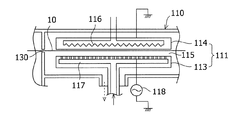
(第1実施形態)
図1は、本発明に係る多層膜形成方法を実施する第1実施形態の成膜装置100を示している。成膜装置100は、長手方向の各端に配設された第1および第2の一対の搬送室(供給/回収部)101,102と、それらの間に列設された第1および第2の2つの成膜室110,120とを備え、基板10を、搬送室101,102の一方から他方に向け各成膜室110,120を通過させてインラインで搬送しながら、各成膜室110,120内にそれぞれ並設された平行平板型の電極対111,112および電極対121,122において前記基板10の表面に気相化学反応により薄膜の層を積層形成するように構成されている。
(First embodiment)
FIG. 1 shows a
第1実施形態における基板10は、プラスチックフィルムなどの帯状の可撓性基板からなる。搬送室101,102には、一方のコア103(104)の周囲にロール状に巻かれた可撓性基板10を巻出し、他方のコア104(103)に巻取るためのコア駆動装置(103,104)、および、それらの間で可撓性基板10を所定の搬送速度かつ搬送張力にて搬送すべく同期して駆動回転されるフィードロール105,106が配設され、さらに、図示を省略するが、基板10の張力を検知するためのテンションロールや、搬送経路上において可撓性基板10を案内するガイドロールなどが設けられている。これら以外に、基板10の幅方向位置を制御する端部位置制御ロールや、可撓性基板10の幅方向端部を把持するグリップローラが付設されていても良い。
The board |
成膜装置100は、両側の搬送室(供給/回収部)101,102間で基板10を双方向に搬送し、往復成膜工程を実施可能となるように、それぞれのコア103,104およびフィードロール105,106はリバーシブルモータによって駆動される。その際、搬送方向に対して下流側に位置したフィードロール(106)のモータをマスターとして速度制御を行い、搬送方向に対して上流側に位置したフィードロール(105)のモータをスレーブとして基板10の搬送張力が一定に維持されるようにトルク制御を行うとともに、各コア103,104のモータを巻出し/巻取り張力が一定に維持されるようにそれぞれトルク制御を行うことで、基板10を所定の搬送速度かつ搬送張力にて連続的に搬送可能である。各フィードロール105,106のモータの可変速運転における速度制御およびトルク制御は、インバータ制御により実施可能である。但し、速度の可変レンジが小さい場合には、閉ループの電圧制御にて実施することもできる。また、DCブラシレスモータを用いることもできる。
The
なお、以下の説明では、便宜的に第1搬送室101から第2搬送室102に向かう方向を正方向とする。また、図示例では、各成膜室110,120および各電極対111,112,121,122は長手方向に同数、同形状で対称に配置されているが、電極対の設置数や電極面積などが長手方向に非対称に配置されていても良い。但し、様々な成膜工程に対する自由度や適用性という点では、図示例のような対称配置が有利である。また、成膜装置100は、基板10を縦姿勢にて横方向に搬送しながら成膜できるように、前記各コア103,104、フィードロール105,106、テンションロール等の回転軸はいずれも鉛直方向に配向されているが、搬送姿勢や搬送方向はこれに限定されるものではない。例えば、平姿勢で横方向や上下方向に搬送するように装置を構成することもできる。
In the following description, for the sake of convenience, the direction from the
可撓性基板10としては、例えば、高耐熱性のポリイミドフィルム(PI)が好適であるが、ポリエーテルイミド(PEI)、ポリエーテルニトリル(PEN)、ポリエーテルサルフォン(PES)、ポリアミド(PA)、ポリアミドイミド(PAI)、ポリエーテルエーテルケトン(PEEK)、ポリエチレンテレフタレート(PET)等の他のプラスチックフィルムを用いることもでき、さらには、アルミニウムやステンレスなどの金属箔を用いることもできる。
For example, a highly heat-resistant polyimide film (PI) is suitable as the
可撓性基板10の厚さは、特に限定されるものではないが、薄い方が材料費を削減できる点で有利である。しかし、基板が薄すぎると、材料によっては加工費が高くなり、また、応力による変形が大きくなり、搬送が困難になる場合があるので、材料に合わせて適正な厚さに選定される必要がある。後述の実施例では、可撓性基板10として、幅500mm、厚さ50μmのポリイミドフィルムを用いたが、可撓性基板10の幅は、装置コストおよび製造コストの点では、膜の均一性が得られる限り広い方が望ましい。
The thickness of the
各成膜室110,120および各搬送室101,102は、相互に気密に結合され、全体として共通室(共通真空室)を構成する一方、それぞれが隔壁によって仕切られ、各室間のコンダクタンスが低減されている。それぞれの隔壁を貫通して基板10を通過可能にするスリット130が設けられ、該スリット130によって各室は相互に連通されているが、各室が個別に排気され、かつ、各室の真空度が略同一に維持されることで、各室相互間におけるガスの流通が抑制されている。スリット130は、例えば、幅500mmの基板10に対して直交する方向に5mmの幅で形成されるが、基板10の搬送精度が高ければより狭くすることができる。但し、各成膜室の圧力が異なると、ガスの相互拡散抑制のためにコストが高いガスゲートなどを用いる必要があるため、圧力は同じものとする。
The
各成膜室110,120内に配設された電極対111,112および電極対121,122は、それぞれが容量結合型のプラズマCVD装置を構成するものであり、基板10の搬送経路を挟んでその両側に平行に配置されたカソード(高周波電極)113,123とアノード(接地電極)114,124とで構成されている。カソード113,123は、共通室の外部に配置された高周波電源118に接続されている。後述の実施例では、各電極対111,112,121,122は、基板幅500mmに対し、搬送方向に300mm、基板幅方向に500mmの平行平板電極で構成される。
The electrode pairs 111 and 112 and the electrode pairs 121 and 122 disposed in the
図3は、プラズマCVD装置を構成する電極対111の好適な実施形態を示している。図3において、カソード113は、表面に多数のガス噴出孔を有する多孔板からなるシャワー電極構造をなしており、背後に画成されたガスチャンバー117内に、共通室の外部からガスを供給することで、カソード113のガス噴出孔を通じて、電極対間の放電成膜領域115にガスを導入可能である。また、アノード114にはヒーターが内蔵されており、アノード114に沿って走行する基板10および放電成膜領域115を加熱可能である。
FIG. 3 shows a preferred embodiment of the
上記のように構成されたカソード113とアノード114との間に高周波電圧を印加することにより、放電成膜領域115にプラズマが形成され、プラズマ中の成膜の前駆体であるラジカルは拡散して、基板10の表面に堆積し、薄膜を形成可能である。このようなシャワー電極構造の電極対111では、ガスの均一な分布が得られるとともに、電極対間の放電成膜領域115に生じるガス流れによって、他の成膜領域で導入されたガスが当該放電成膜領域115に入りにくい。したがって、同一の成膜室110内に設置された他の電極対112において、当該電極対111と組成の近いガスであれば同時に供給し、連続的に成膜可能であり、さらに、成膜時のガス圧力を上昇させることで、成膜室110,120間の隔壁(スリット130)を省略できる場合もある。
By applying a high frequency voltage between the
図6は、第1実施形態の成膜装置100のガス供給系140および真空排気系170を示している。各成膜室110,120内に配設された電極対111,112,121,122の放電成膜領域115,115,125,125へのガス供給系140は、成膜に使用する原料ガスを貯蔵するガスボンベなどからなる多数のガス供給源141,142,143・・・と、第1および第2の流量制御部150,160で構成されている。
FIG. 6 shows the
流量制御部150,160は、ガス供給源141,142,143・・・に対応したマスフローコントローラ155,156,165,166とその前後のガス供給弁153,154,157,158,163,164,167,168とを組み合わせた構成であり、開閉弁151,152,161,162を介して各電極対111,112,121,122のガスチャンバー(117)に接続されている。真空排気系170は、開閉弁171および圧力制御弁172を介して各成膜室110,120に接続された真空ポンプ173で構成され、電極対111,112,121,122毎に配設されている。
The flow
上記構成により、各電極対111,112,121,122に導入すべきガス種に対応したガス供給源141,142,143の配管上のガス供給弁153,154,157,158,163,164,167,168のみを選択的に開くことで、各電極対111,112,121,122に所望の原料ガスを所定の混合比にて流量制御しつつ導入可能である。
With the above configuration, the
次に、図4は、上述した第1実施形態の成膜装置100を用いて本発明方法によって形成可能な多層膜の例としてサブストレート型の薄膜光電変換素子1(薄膜太陽電池)の積層構造を示している。薄膜光電変換素子1は、基板10の上に、金属電極層17、n層16、n/i界面層15、i層14、p/i界面層13、p層12、透明電極層11を順次積層したものであり、1つのpin接合構造1aを含むシングルセルとしての例を示している。
Next, FIG. 4 shows a laminated structure of a substrate type thin film photoelectric conversion element 1 (thin film solar cell) as an example of a multilayer film that can be formed by the method of the present invention using the
上記のような薄膜光電変換素子1においては、p/i界面層13やn/i界面層15の組成は、真性半導体層であるi層14に比べて、各界面層に隣接したドープ層であるp層12やn層16の組成に近い。アモルファスシリコン(a−Si)半導体膜の場合、p型ドーパントとしてはホウ素(B)が、n型ドーパントとしてはリン(P)が、それぞれ添加され、それらを含むジボラン(B2H6)やホスフィン(PH3)などのドーピングガスガスが、主ガスであるシラン(SiH4)や希釈ガスである水素に添加されるが、それらの界面層においても、それぞれのドーピングガスを異なる低濃度で混合したガスが用いられる。そのため、多少のガスの相互拡散があっても(中間領域は形成されるものの)、機能面での影響は小さい。
In the thin film
しかも、これら界面層(13,15)やドープ層(12,16)は、いずれも膜厚がi層(14)の数%と極端に薄く、成膜における堆積速度を考慮しても、それぞれの成膜時間は、i層(14)のそれに比べて短い。そこで、成膜装置100の2つの成膜室110,120に異なる組成のガスを同時に供給して、各界面層(13,15)と、それらに隣接したドープ層(12,16)とを各1回の搬送・成膜工程で同時に連続して成膜することで、これらの成膜工程での搬送速度を、個別に成膜する場合の1/2にでき、i層(14)の搬送・成膜工程での搬送速度との差、すなわち、搬送速度の可変レンジを小さく抑えることができる。
Moreover, the interface layers (13, 15) and the doped layers (12, 16) are extremely thin with a thickness of several percent of the i layer (14). The film formation time of is shorter than that of the i layer (14). Therefore, gases having different compositions are simultaneously supplied to the two
例えば、表1は、図4に示したサブストレート型の薄膜光電変換素子1のpin接合構造1aを構成する各層の膜厚(nm)、堆積速度(nm/sec)、成膜時間(sec)、および搬送速度(mm/sec)を示しており、成膜時間は、i層の800(sec)に対して他の層は120(sec)であり、i層の15%に過ぎない。
For example, Table 1 shows the film thickness (nm), deposition rate (nm / sec), and film formation time (sec) of each layer constituting the

もし仮に、これらの各層(12,13,15,16)を個別に成膜すると、表1の比較例に示されるように、各搬送・成膜工程における搬送速度は10(mm/sec)に設定され、i層(14)の搬送・成膜工程における搬送速度1.5(mm/sec)の6.7倍になる。つまり、各層(12,13,15,16)の搬送・成膜工程における搬送速度を定格とすれば、その1/6以下の搬送速度で成膜工程を実施しなければならない。この場合、搬送速度のばらつきがフルスケールに対して5%であれば、i層(14)の成膜時における膜厚のばらつきは20%程度にもなる。 If each of these layers (12, 13, 15, 16) is individually formed, the transfer speed in each transfer / deposition process is 10 (mm / sec) as shown in the comparative example of Table 1. It is set to 6.7 times the transfer speed 1.5 (mm / sec) in the transfer / film formation process of the i layer (14). That is, if the transfer speed in the transfer / film formation process of each layer (12, 13, 15, 16) is rated, the film formation process must be performed at a transfer speed of 1/6 or less. In this case, if the variation in the conveyance speed is 5% with respect to the full scale, the variation in the film thickness at the time of forming the i layer (14) is about 20%.
これに対して、表1の実施例1に示されるように、各界面層(13,15)と、それらに隣接したドープ層(12,16)とを、各1回の搬送・成膜工程で同時に成膜する場合には、これらの搬送・成膜工程における搬送速度は5(mm/sec)であり、i層(14)の搬送・成膜工程における搬送速度1.5(mm/sec)の3.3倍になり、搬送速度の可変レンジは、個別に成膜する場合の1/2になる。この場合、搬送速度のばらつきが上記同様にフルスケールに対して5%であっても、膜厚のばらつきは4%程度で済む。 On the other hand, as shown in Example 1 of Table 1, each interface layer (13, 15) and the dope layers (12, 16) adjacent thereto are each transported and formed once. In this case, the transfer speed in these transfer / deposition processes is 5 (mm / sec), and the transfer speed in the transfer / deposition process of the i layer (14) is 1.5 (mm / sec). ), And the variable range of the conveyance speed is ½ of that for individual film formation. In this case, even if the variation in the conveyance speed is 5% with respect to the full scale as described above, the variation in the film thickness is only about 4%.
さらに、後述する実施例2または4に示されるように、膜厚の大きいi層(14)の搬送・成膜工程を、2〜3回の搬送・成膜工程に分けて実施すれば、i層(14)の各搬送・成膜工程における搬送速度を3〜4.5(mm/sec)に設定でき、これらの場合、搬送速度の可変レンジは1.67〜1.11倍まで減縮される。また、後述する実用的な薄膜光電変換素子では、p層が条件を変えて2層に分けて成膜されるので、このような場合には膜厚のばらつきを一層低減できると言える。 Further, as shown in Example 2 or 4 to be described later, if the transfer / film formation process of the i-layer (14) having a large film thickness is divided into 2-3 transfer / film formation processes, i The conveyance speed in each conveyance / film formation process of the layer (14) can be set to 3 to 4.5 (mm / sec). In these cases, the variable range of the conveyance speed is reduced to 1.67 to 1.11 times. The In a practical thin film photoelectric conversion element to be described later, the p layer is formed by dividing into two layers under different conditions. In this case, it can be said that the variation in film thickness can be further reduced.
次に、図1に示した第1実施形態の成膜装置100により、図4に示したサブストレート型の薄膜光電変換素子1のpin接合構造1a(光電変換層)を積層形成する具体的な搬送・成膜工程について述べる。なお、この場合、基板10には、先行する成膜工程で、既に、銀(Ag)やアルミニウム(Al)などからなる金属電極層17が形成されており、光電変換層はその上に積層形成される。上述した実施例1のように、各界面層(13,15)と、それらに隣接したドープ層(12,16)とを同一搬送・成膜ステップで連続的に成膜する場合には、pin接合構造1aの成膜に関して、以下のような3つの搬送・成膜ステップを含む。
Next, the
(第1の搬送・成膜ステップ)
先ず、金属電極層17を形成済みの基板10を、第1搬送室101内のロール10aから巻出し、第2搬送室102に向けて正方向に搬送速度5(mm/sec)で搬送しながら、第1成膜室110の各放電成膜領域115に、例えば、主ガスとしてシラン(SiH4)および二酸化炭素(CO2)、希釈ガスとして水素(H2)を用い、n型ドーピングガスとしてホスフィン(PH3)を添加した混合ガスを供給すると同時に、第2成膜室120の各放電成膜領域125に、ドーピングガスを添加せず、二酸化炭素量を減らしかつ低濃度に希釈した主ガスを供給し、第1成膜室110で、プラズマCVD法によりアモルファスシリコンオキサイド(a−SiO)系のn層16を形成し、第2成膜室120では、直前に成膜されたn層16の上にn/i界面層15を積層形成する。このような搬送・成膜ステップの終盤すなわち基板10の終端部では、基板10を走行させたまま、または、基板10を停止した状態で、ドーピングガスを添加せずに、基板10の非成膜領域に対して所定時間の成膜工程を実施し、各成膜室構成部材の少なくとも一部を覆うことで、次プロセスにおけるドーピングガスの部材からの放出を抑制する。
(First transfer / film formation step)
First, the
(第2の搬送・成膜ステップ)
次に、金属電極層17の上にn層16とn/i界面層15が積層形成され、第2搬送室102内にロール10bとして巻き取られた基板10を、該ロール10bから巻出し、第1搬送室101に向けて逆方向に搬送速度1.5(mm/sec)で搬送しながら、第1および第2成膜室110,120の各放電成膜領域115,125に、水素希釈したシラン(SiH4)を供給し、プラズマCVD法により、アモルファスシリコン(a−Si)のi層14を成膜する。
(Second transfer / film formation step)
Next, the
(第3の搬送・成膜ステップ)
次に、金属電極層17の上にn層16、n/i界面層15、i層14が積層形成され、第1搬送室101内にロール10aとして巻き取られた基板10を、該ロール10aから巻出し、第2搬送室102に向けて正方向に搬送速度5(mm/sec)で搬送しながら、第1成膜室110の各放電成膜領域115に、例えば、主ガスとしてシラン(SiH4)および二酸化炭素(CO2)、希釈ガスとして水素(H2)を用い、低濃度に希釈し、かつ、p型ドーピングガスとしてジボラン(B2H6)を少量添加した混合ガスを供給すると同時に、第2成膜室120の各放電成膜領域125に、主ガスとしてシラン(SiH4)および二酸化炭素(CO2)、希釈ガスとして水素(H2)を用い、p型ドーピングガスとしてジボラン(B2H6)を添加し、かつ、前記よりも主ガスの濃度およびドーピングガスの添加量を上昇させた混合ガスを供給し、第1成膜室110で、プラズマCVD法によりアモルファスシリコンオキサイド(a−SiO)系のp/i界面層13を形成し、第2成膜室120では、直前に成膜されたp/i界面層13の上にp層12を積層形成し、第2搬送室102内のロール1bに巻き取る。
(Third transfer / film formation step)
Next, the
上記第3の搬送・成膜ステップにおいて、第2成膜室120内の各電極対121,122に対応したそれぞれの放電成膜領域125において、p型ドーピングガス(B2H6)の添加量を段階的に上昇させたり、二酸化炭素(CO2)の濃度を段階的に減少させたりすることもでき、それらの場合、上記第3の搬送・成膜ステップでは、3種類の層がそれぞれに対応した所定の膜厚で連続的に積層形成されることになる。また、前述したように、i層14の成膜を2回に分けて実施する場合は、上記第2の搬送・成膜ステップを、正逆双方向に搬送速度3(mm/sec)で往復搬送しながら2回実施すれば良い。
In the third transfer / film formation step, the amount of p-type doping gas (B 2 H 6 ) added in each discharge
上述した第1〜第3の搬送・成膜ステップにおけるガス供給を図6に示した第1実施形態の成膜装置100のガス供給系140で実施する場合、図6には、3系統のガス供給源141〜143のみが図示されているが、同様のガス供給源を、例えば、シラン(SiH4)、二酸化炭素(CO2)、水素(H2)ホスフィン(PH3)、および、ジボラン(B2H6)の6系統準備する。
When the gas supply in the first to third transfer / film formation steps described above is performed by the
そして、第1〜第3のそれぞれの搬送・成膜ステップにおいて、第1および第2成膜室110,120のそれぞれで使用するガス種に対応したガス供給弁153,154,157,158,163,164、167,168を選択的に開き、対応するマスフローコントローラ155,156,165,166で流量制御を実施することで、原料ガスの種類、濃度および混合比を切換可能である。なお、各ガス供給源に、所定の希釈度に希釈された原料ガスを準備することもできる。
In each of the first to third transfer / film formation steps,
上記第1実施形態では、サブストレート型の薄膜光電変換素子1のpin接合構造1aを積層形成する搬送・成膜工程について述べたが、基板10の上に金属電極層17を形成する先行工程(一次成膜工程)や、pin接合構造1aの上に、透明電極層11を成膜するのに、成膜装置100を使用することもできる。但し、一次成膜工程の後に、金属電極層17を多数の単位セルに分割するレーザスクライビング工程などが入るので、基板10(ロール)は一旦搬送室101または102から搬出される。また、サブストレート型の薄膜光電変換素子1では、基板10の背面(図4における下面)に直列接続用の金属電極層が形成される場合があり、その成膜工程に上記同様に成膜装置100を使用することもできる。
In the first embodiment, the transfer / film formation process for forming the
また、上記実施形態では、n層およびn/i界面層、p/i界面層およびp層をそれぞれ同一搬送・成膜ステップで連続的に成膜する場合について述べたが、n層およびn/i界面層、または、p/i界面層およびp層のいずれかのみに実施しても良い。また、pin接合構造を構成するシリコン系材料としては、アモルファスシリコン(a−Si)やアモルファスシリコンオサイド(a−SiO)の他に、アモルファスシリコンカーバイド(a−SiC)、アモルファスシリコンナイトライド(a−SiN)など、周知のシリコン系材料を用いることができ、また、微結晶シリコン(μc−Si)薄膜やアモルファス相を含む微結晶シリコン薄膜等であっても良い。 In the above embodiment, the case where the n layer, the n / i interface layer, the p / i interface layer, and the p layer are continuously formed in the same transport / deposition step has been described. The process may be performed only on the i interface layer, or only one of the p / i interface layer and the p layer. In addition to amorphous silicon (a-Si) and amorphous silicon oxide (a-SiO), amorphous silicon carbide (a-SiC), amorphous silicon nitride (a Well-known silicon-based materials such as -SiN) can be used, and a microcrystalline silicon ([mu] c-Si) thin film, a microcrystalline silicon thin film containing an amorphous phase, or the like may be used.
さらに、上記実施形態では、1つのpin接合構造1aを含むシングルセルとしての例を示したが、2つのpin接合構造を積層した2層タンデムや、3つのpin接合構造を積層したトリプルセルなどの多接合構造であっても良い。それらの場合、上記第1〜第3の搬送・成膜ステップが、必要に応じて原料ガスの組成や成膜条件を変更して反復されるので、多接合構造であるほど、本発明に係る多層膜形成方法による製造工程の簡素化、装置負担の軽減、製品品質を安定化などのメリットが大きくなると言える。
Furthermore, in the above embodiment, an example of a single cell including one
(第2実施形態)
図2は、本発明に係る多層膜形成方法を実施する第2実施形態の成膜装置200を示している。成膜装置200は、ガラス基板などの枚葉基板20をインラインで搬送しながら、上述した第1実施形態と同様の往復搬送・成膜ステップを実施するために、長手方向の各端に配設された第1および第2の一対の搬送室(供給/回収部)201,202と、それらの間に列設された第1および第2の2つの成膜室210,220とを備えている。
(Second Embodiment)
FIG. 2 shows a
この成膜装置200は、各成膜室210,220内に並設された平行平板型の電極対211,212および電極対221,222の構成は第1実施形態と同様であるが、各成膜室210,220には、枚葉基板20を搬送経路に沿って所定ピッチでインライン搬送するために、基板20の幅方向端部を把持して送出するローラコンベアまたはベルトコンベアなどからなる不図示の搬送装置が設けられている。
In this
さらに、各搬送室201,202は、多数の枚葉基板20を重ね合わせた状態にストック(20a,20b)し、かつ、ストックされた基板20を一枚ずつ送り出して搬送装置(搬送経路)に供給可能な集積装置として構成されている。なお、各搬送室201,202(集積装置)および搬送装置は、各枚葉基板20を一枚ずつホルダ(キャリア)に保持した状態でストックし、かつ、搬送・成膜できるように構成されても良い。
Further, each
また、直線的な搬送経路の途中に、基板20の搬送方向を変更する機構を備えていても良い。さらには、搬送経路の終端(搬送室202)を始端(搬送室201)に循環させ、1つの搬送・成膜ステップを終了した基板20が、次の搬送・成膜ステップを同じ搬送方向にて実施するために、搬送室201に集積されるように構成することもできる。
Further, a mechanism for changing the transport direction of the
また、図示例では、各成膜室210,220および各電極対211,212,221,222は長手方向に同数、同形状で対称に配置されているが、第1実施形態の場合同様、電極対の設置数や電極面積などが長手方向に非対称に配置されていても良い。さらに、成膜装置200は、基板20を縦姿勢にて横方向に搬送しながら成膜する構成の他に、平姿勢で横方向や上下方向に搬送しながら成膜する構成としても良い。
In the illustrated example, the
上記のように構成された成膜装置200においても、第1実施形態の成膜装置100と同様の搬送・成膜ステップを実施可能であることは、図面からも明らかであるので、ここでは詳細な説明を省略する。また、第2実施形態の成膜装置200は、図4に示したサブストレート型の薄膜光電変換素子1以外に、ガラスなどの透明な枚葉基板を用いたスーパーストレート型の薄膜光電変換素子の搬送・成膜工程に好適に使用可能である。
Since it is also apparent from the drawings that the
図5は、第2実施形態の成膜装置200を用いて本発明方法により形成可能なスーパーストレート型の薄膜光電変換素子2(薄膜太陽電池)の積層構造を示している。図5において、薄膜光電変換素子2は、透明な基板20の上に、透明電極層21、p層22、p/i界面層23、i層24、n/i界面層25、n層26、金属電極層27を順次積層したものであり、1つのpin接合構造2aを含むシングルセルとしての例を示している。
FIG. 5 shows a laminated structure of a super straight type thin film photoelectric conversion element 2 (thin film solar cell) that can be formed by the method of the present invention using the
このスーパーストレート型の薄膜光電変換素子2は、基板20に対するpin接合構造2a向きがサブストレート型と上下逆であるため、成膜順は逆になるが、各界面層(23,25)と、それらに隣接したドープ層(22,26)とを同一搬送・成膜ステップで連続的に成膜し、i層24を別の搬送・成膜ステップで成膜する点は、第1実施形態と同様である。
In this super straight type thin film
すなわち、第1の搬送・成膜ステップで、透明電極層21が形成された基板20を第1搬送室201から第2搬送室202に向けて正方向に搬送しながら、透明電極層21の上にp層22およびp/i界面層23を連続的に積層形成し、次いで、第2の搬送・成膜ステップでは、基板20を逆方向に搬送しながら、p/i界面層23の上にi層24を形成し、さらに、第3の搬送・成膜ステップでは、基板20を再度正方向に搬送しながら、i層24の上にn/i界面層25およびn層26を連続的に積層形成することになる。
That is, in the first transport / film formation step, the
次に、本発明に係る各実施例について述べる。以下の実施形態は基本的に前記第1実施形態に基づいてpin接合構造の搬送・成膜ステップを実施したものであるが、上述したような変更を加えることで前記第2実施形態の実施例ともなりうることは容易に理解されよう。 Next, each embodiment according to the present invention will be described. The following embodiment is basically a transfer and film forming step of a pin junction structure based on the first embodiment. However, by adding the above-described changes, the embodiment of the second embodiment is implemented. It will be easily understood that it can be accompanied.
(実施例2)
表2に示す実施例2では、2つの成膜室110,120を合わせた搬送区間(成膜領域)の長さが2mの成膜装置100を用い、以下のような2往復の搬送・成膜ステップ1〜4を実施し、金属電極層および透明電極層が積層形成された基板上にpin接合構造(光電変換層)の多層膜を形成した。
(Example 2)
In Example 2 shown in Table 2, a
(2.1)搬送・成膜ステップ1
基板10を搬送速度8.4mm/secで正方向に搬送しつつ、第1成膜室110にて、主ガスSiH4:5ml/min、水素希釈度(H2/SiH4)10倍、ドーピングガス添加量(PH3/SiH4)1%、二酸化炭素添加量(CO2/SiH4)1倍としてa−SiO系のn層を成膜し、第2成膜室120にて、主ガスSiH4:5ml/min、水素希釈度(H2/SiH4)25倍、ドーピングガス無添加、二酸化炭素添加量(CO2/SiH4)0.3倍としてn/i層を成膜した。
(2.2)搬送・成膜ステップ2
基板10を搬送速度5.0mm/secで逆方向に搬送しつつ、第1および第2成膜室110,120にて、主ガスSiH4:20ml/min、水素希釈度(H2/SiH4)10倍としてa−Siのi層の1/2を成膜した。
(2.3)搬送・成膜ステップ3
基板10をステップ2と同じ搬送速度5.0mm/secで正方向に搬送しつつステップ2と同じガス条件でa−Siのi層の残余の1/2を成膜した。
(2.4)搬送・成膜ステップ4
基板10を搬送速度8.4mm/secで逆方向に搬送しつつ、第2成膜室120にて、主ガスSiH4:5ml/min、水素希釈度(H2/SiH4)25倍、ドーピングガス添加量(B2H6/SiH4)100ppm、二酸化炭素添加量(CO2/SiH4)0.4倍としてp/i層を成膜し、第1成膜室110の第2電極対112にて、主ガスSiH4:5ml/min、水素希釈度(H2/SiH4)20倍、ドーピングガス添加量(B2H6/SiH4)1%、二酸化炭素添加量(CO2/SiH4)1倍としてa−SiO系のp1層を、第1成膜室110の第1電極対111にて、主ガスSiH4:5ml/min、水素希釈度(H2/SiH4)20倍、ドーピングガス添加量(B2H6/SiH4)2%、二酸化炭素添加量(CO2/SiH4)1倍としてa−SiO系のp2層を成膜した。
(2.1) Transport /
While transporting the
(2.2) Transport /
While the
(2.3) Transport / film formation step 3
The remaining half of the i-layer of a-Si was deposited under the same gas conditions as in
(2.4) Transport / film formation step 4
While the
上記実施例2では、n層とn/i層を搬送・成膜ステップ1で同時に成膜し、最も膜厚の大きいi層を搬送・成膜ステップ2,3に分けて成膜する一方、p/i層と、その1/2の膜厚を有するp1層およびp2層を、搬送・成膜ステップ4で同時に成膜している。この実施例2では、搬送・成膜ステップ2,3の搬送速度(2.5mm/sec)を、i層を1ステップで成膜する場合の搬送速度(1.25mm/sec)の2倍に設定でき、他の搬送・成膜ステップ1,4との搬送速度の差が小さくなっている。また、搬送・成膜ステップ4では、成膜装置100の成膜領域を、第2成膜室120に対応した1/2領域と、第1成膜室110の各電極対111,112に対応した2つの1/4領域の、3つの領域に分け、3層を同時に成膜している。
In Example 2 above, the n layer and the n / i layer are simultaneously formed in the transfer /
(実施例3)
表3に示す実施例3では、実施例2と同様に2つの成膜室110,120を合わせた搬送区間(成膜領域)の長さが2mの成膜装置100を用い、以下のような1.5往復の搬送・成膜ステップ1〜3を実施し、金属電極層および透明電極層が積層形成された基板上にpin接合構造(光電変換層)の多層膜を形成した。
(Example 3)
In Example 3 shown in Table 3, as in Example 2, the
(3.1)搬送・成膜ステップ1
基板10を搬送速度16.6mm/secで正方向に搬送しつつ、第1および第2成膜室110,120にて、主ガスSiH4:10ml/min、水素希釈度(H2/SiH4)25倍、ドーピングガス添加量(PH3/SiH4)4%、二酸化炭素添加量(CO2/SiH4)0.25倍としてa−SiO系のn層を成膜した。
(3.2)搬送・成膜ステップ2
基板10を搬送速度5.2mm/secで逆方向に搬送しつつ、第1および第2成膜室110,120にて、主ガスSiH4:25ml/min、水素希釈度(H2/SiH4)15倍としてi層を成膜した。なお、実施例3では、n/i層が省略された代わりに、i層にごく微量(2ppm)のドーピングガスが添加された。
(3.3)搬送・成膜ステップ3
基板10を搬送速度13.3mm/sec正方向に搬送しつつ、第1成膜室110にて、主ガスSiH4:10ml/min、水素希釈度(H2/SiH4)25倍、ドーピングガス添加量(B2H6/SiH4)200ppm、二酸化炭素添加量(CO2/SiH4)0.35倍としてp/i層を成膜し、第2成膜室120の第1電極対121にて、主ガスSiH4:10ml/min、水素希釈度(H2/SiH4)20倍、ドーピングガス添加量(B2H6/SiH4)1%、二酸化炭素添加量(CO2/SiH4)2倍としてp1層を、第2成膜室120の第2電極対122にて、主ガスSiH4:10ml/min、水素希釈度(H2/SiH4)20倍、ドーピングガス添加量(B2H6/SiH4)2%、二酸化炭素添加量(CO2/SiH4)0.9倍としてp2層を成膜した。
(3.1) Transport /
While transporting the
(3.2) Transport /
While the
(3.3) Transport / film formation step 3
While transporting the
上記実施例3では、i層の膜厚が先行する実施例に比べて小さいことから、i層は1回の搬送・成膜ステップで成膜するものとしてステップ数を3回に留め、処理工程の簡素化を図っている。 In the third embodiment, since the thickness of the i layer is smaller than that of the preceding embodiment, the i layer is formed in one transfer / deposition step, and the number of steps is limited to three. Simplification.
(実施例4)
表4に示す実施例4では、搬送方向の長さが均等でない3つの成膜室を備え、第1成膜室に2つ、第2成膜室に3つの電極対がそれぞれ並設され、第3成膜室には3つのハーフサイズの電極対が並設され、第1〜第3成膜室を合わせた搬送区間(成膜領域)の長さが3mである成膜装置を用い、以下のような3往復の搬送・成膜ステップ1〜6を実施し、金属電極層および透明電極層が積層形成された基板上にpin接合構造(光電変換層)の多層膜を形成した。
Example 4
In Example 4 shown in Table 4, the length in the transport direction is provided with three film formation chambers, two electrode pairs in the first film formation chamber and three electrode pairs in the second film formation chamber, In the third film forming chamber, three half-size electrode pairs are arranged side by side, and a film forming apparatus in which the length of the transfer section (film forming region) including the first to third film forming chambers is 3 m is used. The following three reciprocating conveyance / film formation steps 1 to 6 were performed, and a multilayer film having a pin junction structure (photoelectric conversion layer) was formed on the substrate on which the metal electrode layer and the transparent electrode layer were laminated.
(4.1)搬送・成膜ステップ1
基板を搬送速度15.8mm/secで正方向に搬送しつつ、第1成膜室にて、主ガスSiH4:20ml/min、水素希釈度(H2/SiH4)5倍、ドーピングガス添加量(PH3/SiH4)4%、二酸化炭素添加量(CO2/SiH4)1倍としてa−SiO系のn層を成膜し、第2および第3成膜室にて、主ガスSiH4:20ml/min(各室10ml/min)、水素希釈度(H2/SiH4)25倍、ドーピングガスおよび二酸化炭素を添加しないでn/i層を成膜した。
(4.2)搬送・成膜ステップ2
基板を搬送速度25.0mm/secで逆方向に搬送しつつ、第3成膜室の第2第3電極対にて、主ガスSiH4:10ml/min、水素希釈度(H2/SiH4)200倍としてμc−Siのi1層を成膜し、第3成膜室の第1電極対と第2および第1成膜室にて、主ガスSiH4:20ml/min、水素希釈度(H2/SiH4)100倍としてμc−Siのi層の10%を成膜した。
(4.3)搬送・成膜ステップ3
基板を搬送速度10.0mm/secで正方向に搬送しつつ、第1〜第3成膜室にて、主ガスSiH4:20ml/min、水素希釈度(H2/SiH4)100倍としてμc−Siのi層の30%を成膜した。
(4.4)搬送・成膜ステップ4
基板を搬送速度10.0mm/secで逆方向に搬送しつつ、第1〜第3成膜室にて、前記同様に主ガスSiH4:20ml/min、水素希釈度(H2/SiH4)100倍としてμc−Siのi層の30%を成膜した。
(4.5)搬送・成膜ステップ5
基板を搬送速度10.0mm/secで正方向に搬送しつつ、第1〜第3成膜室にて、前記同様に主ガスSiH4:20ml/min、水素希釈度(H2/SiH4)100倍としてμc−Siのi層の残余の30%を成膜した。
(4.6)搬送・成膜ステップ6
基板を搬送速度18.8mm/secで逆方向に搬送しつつ、第3成膜室の第3電極対にて、主ガスSiH4:5ml/min、水素希釈度(H2/SiH4)25倍、ドーピングガス添加量(B2H6/SiH4)100ppmとしてp/i層を、第3成膜室の第2および第1電極対にて、主ガスSiH4:5ml/min、水素希釈度(H2/SiH4)20倍、ドーピングガス添加量(B2H6/SiH4)1%としてa−Siのp1層を成膜し、第2および1成膜室にて、主ガスSiH4:5ml/min、水素希釈度(H2/SiH4)250倍、ドーピングガス添加量(B2H6/SiH4)2%としてμc−Siのp2層を成膜した。
(4.1) Transport /
While transporting the substrate in the forward direction at a transport speed of 15.8 mm / sec, main gas SiH 4 : 20 ml / min, hydrogen dilution (H 2 / SiH 4 ) 5 times, doping gas added in the first film formation chamber An a-SiO-based n-layer was formed with an amount (PH 3 / SiH 4 ) of 4% and a carbon dioxide addition amount (CO 2 / SiH 4 ) of 1 and the main gas was formed in the second and third film formation chambers. SiH 4 : 20 ml / min (each
(4.2) Transport /
While transporting the substrate in the reverse direction at a transport speed of 25.0 mm / sec, the main gas SiH 4 : 10 ml / min, hydrogen dilution (H 2 / SiH 4) at the second third electrode pair in the third film formation chamber. ) An i1 layer of μc-Si is formed 200 times, and the main gas SiH 4 : 20 ml / min, hydrogen dilution (in the first electrode pair and the second and first film forming chambers in the third film forming chamber) H 2 / SiH 4 ) 100 times, 10% of the μc-Si i layer was formed.
(4.3) Transport / film formation step 3
While the substrate is transported in the forward direction at a transport speed of 10.0 mm / sec, the
(4.4) Transport / film formation step 4
While transferring the substrate in the reverse direction at a transfer speed of 10.0 mm / sec, in the first to third film forming chambers, the main gas SiH 4 : 20 ml / min and the hydrogen dilution (H 2 / SiH 4 ) in the same manner as described above. As a result, 30% of the i-layer of μc-Si was deposited.
(4.5) Transport / film formation step 5
While transferring the substrate in the forward direction at a transfer speed of 10.0 mm / sec, in the first to third film forming chambers, the main gas SiH 4 : 20 ml / min and the hydrogen dilution (H 2 / SiH 4 ) as described above. The remaining 30% of the i-layer of μc-Si was deposited at 100 times.
(4.6) Transport / film formation step 6
While transporting the substrate in the reverse direction at a transport speed of 18.8 mm / sec, the main gas SiH 4 : 5 ml / min, hydrogen dilution (H 2 / SiH 4 ) 25 at the third electrode pair in the third deposition chamber. The doping gas addition amount (B 2 H 6 / SiH 4 ) is 100 ppm, and the p / i layer is diluted with the main gas SiH 4 : 5 ml / min at the second and first electrode pairs in the third film formation chamber, diluted with hydrogen. A-Si p1 layer was deposited at a rate of 20 times (H 2 / SiH 4 ) and a doping gas addition amount (B 2 H 6 / SiH 4 ) of 1%, and the main gas was formed in the second and first deposition chambers. A μc-Si p2 layer was formed with SiH 4 : 5 ml / min, hydrogen dilution (H 2 / SiH 4 ) 250 times, doping gas addition amount (B 2 H 6 / SiH 4 ) 2%.
上記実施例4では、n層とn/i層を搬送・成膜ステップ1で同時に成膜し、最も膜厚の大きいi層の10%と、そのn/i層側に介在する相対的に低濃度のi1層とを搬送・成膜ステップ2で同時に成膜し、さらに、i層の残余の90%を搬送・成膜ステップ3〜5に分けて成膜した後、p/i層、p1層およびp2層を、搬送・成膜ステップ6で同時に成膜している。
In Example 4 above, the n layer and the n / i layer are simultaneously formed in the transfer /
上記各実施例1〜4の多層膜形成プロセスで得られたpin接合構造の光電変換層の上に透明電極層を形成した光電変換セルは、比較例のように各層を個別に成膜した光電変換層の上に透明電極層を形成した同構造の光電変換セルと比較しても、発電効率等の性能面で差は見られず、その一方で、格段に簡素化された搬送・成膜ステップで効率良く製造可能であるとともに、搬送速度の可変レンジが小さく抑えられたことで、膜厚のばらつきが抑制され、製品品質の安定化が期待できる。 The photoelectric conversion cell in which the transparent electrode layer is formed on the photoelectric conversion layer having the pin junction structure obtained by the multilayer film formation process of each of the above Examples 1 to 4 is formed by individually forming each layer as in the comparative example. Compared to a photoelectric conversion cell with the same structure in which a transparent electrode layer is formed on the conversion layer, there is no difference in performance such as power generation efficiency, but on the other hand, the transport and film formation is greatly simplified. It can be manufactured efficiently in steps, and the variable range of the conveyance speed is kept small, so that variations in film thickness are suppressed, and stabilization of product quality can be expected.
以上、本発明のいくつかの実施形態について述べたが、本発明は上記に限定されるものではなく、上記以外にも本発明の技術的思想に基づいてさらに各種の変形および変更が可能である。 Although several embodiments of the present invention have been described above, the present invention is not limited to the above, and various modifications and changes can be made based on the technical idea of the present invention other than the above. .
例えば、上記各実施形態では、成膜装置100,200に、容量結合型のプラズマCVDを用いる場合を示したが、表面波プラズマCVD(SWP−CVD)や、触媒CVD(Cat−CVD)、あるいは、電子サイクロトロン共鳴プラズマCVD(ECR−CVD)を利用したものであっても良い。但し、ガスを原料としないスパッタなどの物理蒸着(PVD)は、複数の層を連続的に成膜することに困難はなく、本発明の範囲外である。
For example, in each of the above embodiments, the case where capacitively coupled plasma CVD is used for the
本発明に係る多層膜形成方法は、薄膜光電変換素子の製造工程に限定されるものではなく、膜厚の異なる多くの層を含む他の多層膜の製造工程にも利用可能である。 The multilayer film forming method according to the present invention is not limited to the manufacturing process of the thin film photoelectric conversion element, but can be used for the manufacturing process of other multilayer films including many layers having different film thicknesses.
1,2 薄膜光電変換素子
1a,2a pin接合構造
10,20 基板
11,21 透明電極層
12,22 p層
13,23 p/i界面層
14,24 i層
15,25 n/i界面層
16,26 n層
17,27 金属電極層
100,200 成膜装置
101,102,201,202 搬送室
103,104 コア(コア駆動装置)
105,106 フィードロール
110,120,210,220 成膜室
111,112,121,122,211,212,221,222 電極対
113,123,213,223 カソード(高周波電極)
114,124,214,224 アノード(接地電極)
115,125,215,225 放電成膜領域
140 ガス供給系
141,142,143 ガス供給源
150,160 流量制御部
151,152,161,162 開閉弁
153,154,157,158,163,164,167,168 ガス供給弁
155,156,165,166 マスフローコントローラ
170 真空排気系
171 開閉弁
172 圧力制御弁
173 真空ポンプ
DESCRIPTION OF
105, 106 Feed rolls 110, 120, 210, 220
114, 124, 214, 224 Anode (ground electrode)
115, 125, 215, 225 Discharge
Claims (17)
前記基板の搬送経路に沿って少なくとも第1および第2の成膜部を有し、前記搬送経路の各端に前記基板の供給/回収部を有する成膜装置を準備するステップと、
前記基板を前記搬送経路に沿って第1の速度で連続的に搬送しつつ、前記第1および第2の各成膜部に、相互に組成が近い第1および第2の原料ガスを同時に供給して、相互に組成が近い第1および第2層を含む複数の層を積層形成する第1の搬送・成膜ステップと、
前記第1の搬送・成膜ステップの前または後で、前記基板を前記搬送経路に沿って第2の速度で連続的に搬送しつつ、前記第1および第2の各成膜部に、前記第1および第2の原料ガスと組成が異なりかつ相互に実質的に組成が同一である第3の原料ガスを供給して、前記第1および第2層と組成が異なる第3層を形成する第2の搬送・成膜ステップと、
を含む、多層膜形成方法。 A multilayer film forming method in which three or more layers having different composition of source gas are formed on at least one surface of a substrate by a gas phase chemical reaction,
Preparing a film forming apparatus having at least first and second film forming units along the substrate transfer path and having the substrate supply / recovery unit at each end of the transfer path;
While the substrate is continuously transported along the transport path at a first speed, first and second source gases having compositions close to each other are simultaneously supplied to the first and second film forming units. A first transporting and film-forming step in which a plurality of layers including a first layer and a second layer having a composition close to each other are stacked;
Before or after the first transport / film formation step, the substrate is transported continuously at a second speed along the transport path, while the first and second film forming units A third source gas having a composition different from that of the first and second source gases and substantially the same as each other is supplied to form a third layer having a composition different from that of the first and second layers. A second transfer / film formation step;
A multilayer film forming method comprising:
前記基板を正逆双方向に所定の搬送速度で連続的に搬送可能な搬送装置と、
前記基板の搬送経路の第1および第2端に配設され、前記基板を供給しかつ回収可能な第1および第2の供給/回収部と、
前記基板の搬送経路に沿って配設され、前記基板が通過可能なスリットを介して相互に連通された第1および第2の成膜部と、
前記第1および第2の成膜部に原料ガスを個別に供給するためのガス供給手段と、
前記第1および第2の成膜部を個別に排気するための真空排気手段と、
を備え、
前記ガス供給手段は、前記第1および第2の成膜部に、相互に組成が近い第1および第2の原料ガスを同時に供給する第1のガス供給モードと、前記第1および第2の成膜部に、前記第1および第2の原料ガスと組成が異なりかつ相互に実質的に組成が同一である第3の原料ガスを供給する第2のガス供給モードと、を切り換える手段を含む、成膜装置。 A film forming apparatus for carrying out a multilayer film forming method for forming three or more layers having different raw material gas compositions on at least one surface of a substrate by a gas phase chemical reaction,
A transport apparatus capable of continuously transporting the substrate in the forward and reverse directions at a predetermined transport speed;
First and second supply / recovery units disposed at the first and second ends of the substrate transport path and capable of supplying and recovering the substrate;
First and second film forming units disposed along a transport path of the substrate and communicated with each other via a slit through which the substrate can pass;
Gas supply means for individually supplying source gases to the first and second film forming units;
Vacuum evacuation means for individually evacuating the first and second film forming units;
With
The gas supply means includes a first gas supply mode in which first and second source gases having compositions close to each other are simultaneously supplied to the first and second film forming units; The film forming unit includes means for switching between a second gas supply mode for supplying a third source gas having a composition different from that of the first and second source gases and substantially the same as each other. , Film formation equipment.
前記第1および第2の供給/回収部は、前記基板をロールから巻出しかつロールに巻取るための第1および第2のコア駆動装置を含み、
前記搬送装置は、前記第1の成膜部と前記第1のコア駆動装置との間に配設された第1のフィードロールと、前記第2の成膜部と前記第2のコア駆動装置との間に配設された第2のフィードロールと、前記第1のフィードロールを駆動する第1のモータと、前記第2のフィードロールを駆動する第2のモータと、を含み、
前記各モータは、正逆双方向に回転可能かつ回転速度を可変である、請求項15に記載の成膜装置。 The substrate is a flexible substrate having a long strip shape,
The first and second supply / recovery units include first and second core driving devices for unwinding the substrate from the roll and winding it on the roll,
The transfer device includes a first feed roll disposed between the first film forming unit and the first core driving device, the second film forming unit, and the second core driving device. A second feed roll disposed between the first feed roll, a first motor that drives the first feed roll, and a second motor that drives the second feed roll,
The film forming apparatus according to claim 15, wherein each of the motors is rotatable in both forward and reverse directions and has a variable rotation speed.
Priority Applications (4)
| Application Number | Priority Date | Filing Date | Title |
|---|---|---|---|
| JP2010183974A JP2012043983A (en) | 2010-08-19 | 2010-08-19 | Multilayer film forming method and film forming apparatus using the same |
| DE102011110410A DE102011110410A1 (en) | 2010-08-19 | 2011-08-12 | Multilayer film formation method and film deposition apparatus used with the method |
| US13/212,571 US20120045864A1 (en) | 2010-08-19 | 2011-08-18 | Multilayer film formation method and film deposition apparatus used with the method |
| CN2011102802821A CN102376550A (en) | 2010-08-19 | 2011-08-19 | Multilayer film formation method and film deposition apparatus used with the method |
Applications Claiming Priority (1)
| Application Number | Priority Date | Filing Date | Title |
|---|---|---|---|
| JP2010183974A JP2012043983A (en) | 2010-08-19 | 2010-08-19 | Multilayer film forming method and film forming apparatus using the same |
Publications (1)
| Publication Number | Publication Date |
|---|---|
| JP2012043983A true JP2012043983A (en) | 2012-03-01 |
Family
ID=45594385
Family Applications (1)
| Application Number | Title | Priority Date | Filing Date |
|---|---|---|---|
| JP2010183974A Withdrawn JP2012043983A (en) | 2010-08-19 | 2010-08-19 | Multilayer film forming method and film forming apparatus using the same |
Country Status (4)
| Country | Link |
|---|---|
| US (1) | US20120045864A1 (en) |
| JP (1) | JP2012043983A (en) |
| CN (1) | CN102376550A (en) |
| DE (1) | DE102011110410A1 (en) |
Cited By (3)
| Publication number | Priority date | Publication date | Assignee | Title |
|---|---|---|---|---|
| JP2014003275A (en) * | 2012-06-14 | 2014-01-09 | Nexpower Technology Corp | Thin-film solar cell and method of manufacturing the same |
| JP2018532231A (en) * | 2015-10-02 | 2018-11-01 | アプライド マテリアルズ インコーポレイテッドApplied Materials,Incorporated | Method and apparatus for manufacturing a flexible layer stack and flexible layer stack |
| JP2019019384A (en) * | 2017-07-19 | 2019-02-07 | トヨタ自動車株式会社 | Processing apparatus |
Families Citing this family (7)
| Publication number | Priority date | Publication date | Assignee | Title |
|---|---|---|---|---|
| JP6047308B2 (en) * | 2012-05-28 | 2016-12-21 | 日精エー・エス・ビー機械株式会社 | Resin container coating equipment |
| CN102877026B (en) * | 2012-09-27 | 2014-12-24 | 中国科学院长春光学精密机械与物理研究所 | Vacuum depositing device for multilayer film devices |
| AU2014228822A1 (en) | 2013-03-15 | 2015-10-01 | Memorial Sloan-Kettering Cancer Center | HSP90-targeted cardiac imaging and therapy |
| WO2020025102A1 (en) * | 2018-07-30 | 2020-02-06 | Applied Materials, Inc. | Method of coating a flexible substrate with a stack of layers, layer stack, and deposition apparatus for coating a flexible substrate with a stack of layers |
| NL2021997B1 (en) * | 2018-11-14 | 2020-05-20 | Johannes Hendrikus Lagarde Kevin | System and method for depositing a first and second layer on a substrate. |
| CN111261634A (en) * | 2020-02-10 | 2020-06-09 | 无锡拍字节科技有限公司 | Manufacturing equipment and method of memory device |
| CN111739971B (en) * | 2020-08-03 | 2021-02-19 | 苏州迈正科技有限公司 | Film coating equipment, method and system, solar cell, assembly and power generation system |
Citations (4)
| Publication number | Priority date | Publication date | Assignee | Title |
|---|---|---|---|---|
| JPH06132237A (en) * | 1992-10-21 | 1994-05-13 | Canon Inc | Equipment for continuous production of functional deposit film |
| JP2002009313A (en) * | 2000-06-20 | 2002-01-11 | Fuji Electric Co Ltd | Thin-film solar battery |
| JP2003007146A (en) * | 2001-06-22 | 2003-01-10 | Fujikura Ltd | Oxide super conductor and method of manufacturing the same |
| JP2009094399A (en) * | 2007-10-11 | 2009-04-30 | Fuji Electric Systems Co Ltd | Manufacturing apparatus of thin film solar cell |
Family Cites Families (11)
| Publication number | Priority date | Publication date | Assignee | Title |
|---|---|---|---|---|
| JPH03255903A (en) | 1990-03-06 | 1991-11-14 | Yokogawa Electric Corp | Interference signal processing method of absolute length measuring instrument |
| JP2824808B2 (en) * | 1990-11-16 | 1998-11-18 | キヤノン株式会社 | Apparatus for continuously forming large-area functional deposited films by microwave plasma CVD |
| JP3073327B2 (en) * | 1992-06-30 | 2000-08-07 | キヤノン株式会社 | Deposition film formation method |
| JP3169337B2 (en) * | 1995-05-30 | 2001-05-21 | キヤノン株式会社 | Photovoltaic element and method for manufacturing the same |
| JPH1022518A (en) | 1996-07-02 | 1998-01-23 | Sharp Corp | Chemical vapor detection equipment |
| JP3475752B2 (en) | 1997-11-06 | 2003-12-08 | 富士電機ホールディングス株式会社 | Thin film manufacturing equipment |
| JPH11219947A (en) * | 1998-01-29 | 1999-08-10 | Chul-Ju Hwang | Formation of thin film in semiconductor element |
| JP2000183380A (en) | 1998-12-16 | 2000-06-30 | Toppan Printing Co Ltd | Method and apparatus for film-formation of solar cell |
| TW526545B (en) * | 2002-02-05 | 2003-04-01 | Winbond Electronics Corp | Method for using pressure to determine the end point of gas cleaning and method of determination thereof |
| JP4844086B2 (en) * | 2005-10-28 | 2011-12-21 | 三菱電機株式会社 | Semiconductor manufacturing method and satellite |
| TWI348730B (en) * | 2007-07-17 | 2011-09-11 | Ind Tech Res Inst | Method of fabricating polysilicon film |
-
2010
- 2010-08-19 JP JP2010183974A patent/JP2012043983A/en not_active Withdrawn
-
2011
- 2011-08-12 DE DE102011110410A patent/DE102011110410A1/en not_active Withdrawn
- 2011-08-18 US US13/212,571 patent/US20120045864A1/en not_active Abandoned
- 2011-08-19 CN CN2011102802821A patent/CN102376550A/en active Pending
Patent Citations (4)
| Publication number | Priority date | Publication date | Assignee | Title |
|---|---|---|---|---|
| JPH06132237A (en) * | 1992-10-21 | 1994-05-13 | Canon Inc | Equipment for continuous production of functional deposit film |
| JP2002009313A (en) * | 2000-06-20 | 2002-01-11 | Fuji Electric Co Ltd | Thin-film solar battery |
| JP2003007146A (en) * | 2001-06-22 | 2003-01-10 | Fujikura Ltd | Oxide super conductor and method of manufacturing the same |
| JP2009094399A (en) * | 2007-10-11 | 2009-04-30 | Fuji Electric Systems Co Ltd | Manufacturing apparatus of thin film solar cell |
Cited By (4)
| Publication number | Priority date | Publication date | Assignee | Title |
|---|---|---|---|---|
| JP2014003275A (en) * | 2012-06-14 | 2014-01-09 | Nexpower Technology Corp | Thin-film solar cell and method of manufacturing the same |
| JP2018532231A (en) * | 2015-10-02 | 2018-11-01 | アプライド マテリアルズ インコーポレイテッドApplied Materials,Incorporated | Method and apparatus for manufacturing a flexible layer stack and flexible layer stack |
| JP7023222B2 (en) | 2015-10-02 | 2022-02-21 | アプライド マテリアルズ インコーポレイテッド | Methods and equipment for manufacturing flexible layer stacks, as well as flexible layer stacks. |
| JP2019019384A (en) * | 2017-07-19 | 2019-02-07 | トヨタ自動車株式会社 | Processing apparatus |
Also Published As
| Publication number | Publication date |
|---|---|
| CN102376550A (en) | 2012-03-14 |
| US20120045864A1 (en) | 2012-02-23 |
| DE102011110410A1 (en) | 2012-03-29 |
Similar Documents
| Publication | Publication Date | Title |
|---|---|---|
| JP2012043983A (en) | Multilayer film forming method and film forming apparatus using the same | |
| JP4316767B2 (en) | Substrate processing equipment | |
| JP5182610B2 (en) | Thin film solar cell manufacturing equipment | |
| JP5101029B2 (en) | Photoelectric conversion element manufacturing apparatus and photoelectric conversion element manufacturing method | |
| TW200837214A (en) | Deposition system and method | |
| US20110041765A1 (en) | Film deposition device | |
| JPH11214729A (en) | Manufacture of photoelectric conversion device and photoelectric conversion device manufacturing device | |
| JP2009179838A (en) | Thin film production apparatus | |
| EP2256782B1 (en) | Plasma deposition source and method for depositing thin films | |
| JP2001110729A (en) | Apparratus for continuously manufacturing method of semiconductor element | |
| US7588957B2 (en) | CVD process gas flow, pumping and/or boosting | |
| JP5122805B2 (en) | Deposition equipment | |
| US20110262641A1 (en) | Inline chemical vapor deposition system | |
| JP2007266094A (en) | Plasma cvd device and method for forming semiconductor thin-film by same | |
| JP2013505564A (en) | Modular substrate processing system and module substrate processing method | |
| JP5029041B2 (en) | Plasma CVD apparatus and thin film manufacturing method | |
| US11680319B2 (en) | Atomic layer deposition device and atomic layer deposition method | |
| JP2014523479A (en) | In-line chemical vapor deposition method and system | |
| JP4273382B2 (en) | Plasma processing apparatus and thin film forming method | |
| JP4949695B2 (en) | Photoelectric conversion device manufacturing apparatus and photoelectric conversion device manufacturing method | |
| JP4576190B2 (en) | Plasma processing equipment | |
| JP5023914B2 (en) | Thin film manufacturing apparatus and thin film manufacturing method | |
| JP5262338B2 (en) | Plasma CVD equipment | |
| JP2006124784A (en) | Vacuum system and method for exhausting vacuum chamber | |
| JP5169068B2 (en) | Thin film solar cell manufacturing equipment |
Legal Events
| Date | Code | Title | Description |
|---|---|---|---|
| A621 | Written request for application examination |
Free format text: JAPANESE INTERMEDIATE CODE: A621 Effective date: 20130614 |
|
| A977 | Report on retrieval |
Free format text: JAPANESE INTERMEDIATE CODE: A971007 Effective date: 20131218 |
|
| A977 | Report on retrieval |
Free format text: JAPANESE INTERMEDIATE CODE: A971007 Effective date: 20140107 |
|
| A131 | Notification of reasons for refusal |
Free format text: JAPANESE INTERMEDIATE CODE: A131 Effective date: 20140110 |
|
| A761 | Written withdrawal of application |
Free format text: JAPANESE INTERMEDIATE CODE: A761 Effective date: 20140310 |