JP2012027479A - Light-emitting device and electronic apparatus - Google Patents
Light-emitting device and electronic apparatus Download PDFInfo
- Publication number
- JP2012027479A JP2012027479A JP2011187031A JP2011187031A JP2012027479A JP 2012027479 A JP2012027479 A JP 2012027479A JP 2011187031 A JP2011187031 A JP 2011187031A JP 2011187031 A JP2011187031 A JP 2011187031A JP 2012027479 A JP2012027479 A JP 2012027479A
- Authority
- JP
- Japan
- Prior art keywords
- period
- film
- tft
- driving
- signal line
- Prior art date
- Legal status (The legal status is an assumption and is not a legal conclusion. Google has not performed a legal analysis and makes no representation as to the accuracy of the status listed.)
- Withdrawn
Links
- 239000003990 capacitor Substances 0.000 claims abstract description 74
- 239000004065 semiconductor Substances 0.000 claims description 21
- 238000000034 method Methods 0.000 abstract description 132
- 238000005401 electroluminescence Methods 0.000 description 208
- 239000010408 film Substances 0.000 description 160
- 239000010410 layer Substances 0.000 description 118
- 238000003860 storage Methods 0.000 description 66
- 239000000463 material Substances 0.000 description 42
- 239000012535 impurity Substances 0.000 description 36
- 239000000758 substrate Substances 0.000 description 22
- 238000005530 etching Methods 0.000 description 18
- 239000011229 interlayer Substances 0.000 description 16
- XUIMIQQOPSSXEZ-UHFFFAOYSA-N Silicon Chemical compound [Si] XUIMIQQOPSSXEZ-UHFFFAOYSA-N 0.000 description 15
- 238000002347 injection Methods 0.000 description 15
- 239000007924 injection Substances 0.000 description 15
- 238000004519 manufacturing process Methods 0.000 description 15
- 239000011159 matrix material Substances 0.000 description 15
- 229910052710 silicon Inorganic materials 0.000 description 15
- 239000010703 silicon Substances 0.000 description 15
- 239000000945 filler Substances 0.000 description 12
- 239000003566 sealing material Substances 0.000 description 12
- 230000008569 process Effects 0.000 description 10
- 229920005989 resin Polymers 0.000 description 10
- 239000011347 resin Substances 0.000 description 10
- 230000015572 biosynthetic process Effects 0.000 description 9
- 238000010586 diagram Methods 0.000 description 8
- PQXKHYXIUOZZFA-UHFFFAOYSA-M lithium fluoride Chemical class [Li+].[F-] PQXKHYXIUOZZFA-UHFFFAOYSA-M 0.000 description 8
- 238000002161 passivation Methods 0.000 description 8
- 229910052782 aluminium Inorganic materials 0.000 description 7
- 230000006866 deterioration Effects 0.000 description 7
- XAGFODPZIPBFFR-UHFFFAOYSA-N aluminium Chemical compound [Al] XAGFODPZIPBFFR-UHFFFAOYSA-N 0.000 description 6
- 239000012298 atmosphere Substances 0.000 description 6
- 239000000460 chlorine Substances 0.000 description 6
- 239000007789 gas Substances 0.000 description 6
- 229920000642 polymer Polymers 0.000 description 6
- 125000006850 spacer group Chemical group 0.000 description 6
- OAICVXFJPJFONN-UHFFFAOYSA-N Phosphorus Chemical compound [P] OAICVXFJPJFONN-UHFFFAOYSA-N 0.000 description 5
- XLOMVQKBTHCTTD-UHFFFAOYSA-N Zinc monoxide Chemical compound [Zn]=O XLOMVQKBTHCTTD-UHFFFAOYSA-N 0.000 description 5
- 150000001875 compounds Chemical class 0.000 description 5
- 230000000694 effects Effects 0.000 description 5
- 229910003437 indium oxide Inorganic materials 0.000 description 5
- PJXISJQVUVHSOJ-UHFFFAOYSA-N indium(iii) oxide Chemical compound [O-2].[O-2].[O-2].[In+3].[In+3] PJXISJQVUVHSOJ-UHFFFAOYSA-N 0.000 description 5
- 150000002500 ions Chemical class 0.000 description 5
- 229910021420 polycrystalline silicon Inorganic materials 0.000 description 5
- 230000001681 protective effect Effects 0.000 description 5
- 238000004544 sputter deposition Methods 0.000 description 5
- 229910052715 tantalum Inorganic materials 0.000 description 5
- 229910052581 Si3N4 Inorganic materials 0.000 description 4
- VYPSYNLAJGMNEJ-UHFFFAOYSA-N Silicium dioxide Chemical compound O=[Si]=O VYPSYNLAJGMNEJ-UHFFFAOYSA-N 0.000 description 4
- NIXOWILDQLNWCW-UHFFFAOYSA-N acrylic acid group Chemical group C(C=C)(=O)O NIXOWILDQLNWCW-UHFFFAOYSA-N 0.000 description 4
- 238000000137 annealing Methods 0.000 description 4
- QVGXLLKOCUKJST-UHFFFAOYSA-N atomic oxygen Chemical compound [O] QVGXLLKOCUKJST-UHFFFAOYSA-N 0.000 description 4
- 239000000969 carrier Substances 0.000 description 4
- 238000006243 chemical reaction Methods 0.000 description 4
- 238000002425 crystallisation Methods 0.000 description 4
- 230000007423 decrease Effects 0.000 description 4
- 239000011521 glass Substances 0.000 description 4
- PCHJSUWPFVWCPO-UHFFFAOYSA-N gold Chemical group [Au] PCHJSUWPFVWCPO-UHFFFAOYSA-N 0.000 description 4
- 229910052737 gold Inorganic materials 0.000 description 4
- 239000010931 gold Substances 0.000 description 4
- 239000001301 oxygen Substances 0.000 description 4
- 229910052760 oxygen Inorganic materials 0.000 description 4
- 229910052698 phosphorus Inorganic materials 0.000 description 4
- 239000011574 phosphorus Substances 0.000 description 4
- HQVNEWCFYHHQES-UHFFFAOYSA-N silicon nitride Chemical compound N12[Si]34N5[Si]62N3[Si]51N64 HQVNEWCFYHHQES-UHFFFAOYSA-N 0.000 description 4
- 229910052814 silicon oxide Inorganic materials 0.000 description 4
- MZLGASXMSKOWSE-UHFFFAOYSA-N tantalum nitride Chemical compound [Ta]#N MZLGASXMSKOWSE-UHFFFAOYSA-N 0.000 description 4
- UFHFLCQGNIYNRP-UHFFFAOYSA-N Hydrogen Chemical compound [H][H] UFHFLCQGNIYNRP-UHFFFAOYSA-N 0.000 description 3
- 230000001133 acceleration Effects 0.000 description 3
- QVQLCTNNEUAWMS-UHFFFAOYSA-N barium oxide Chemical compound [Ba]=O QVQLCTNNEUAWMS-UHFFFAOYSA-N 0.000 description 3
- 230000005540 biological transmission Effects 0.000 description 3
- DQXBYHZEEUGOBF-UHFFFAOYSA-N but-3-enoic acid;ethene Chemical compound C=C.OC(=O)CC=C DQXBYHZEEUGOBF-UHFFFAOYSA-N 0.000 description 3
- 230000008025 crystallization Effects 0.000 description 3
- 239000005038 ethylene vinyl acetate Substances 0.000 description 3
- 230000005525 hole transport Effects 0.000 description 3
- 239000001257 hydrogen Substances 0.000 description 3
- 229910052739 hydrogen Inorganic materials 0.000 description 3
- 238000009616 inductively coupled plasma Methods 0.000 description 3
- 239000004973 liquid crystal related substance Substances 0.000 description 3
- 230000010355 oscillation Effects 0.000 description 3
- 238000000059 patterning Methods 0.000 description 3
- 238000005268 plasma chemical vapour deposition Methods 0.000 description 3
- 229920001200 poly(ethylene-vinyl acetate) Polymers 0.000 description 3
- 229920002037 poly(vinyl butyral) polymer Polymers 0.000 description 3
- 239000002861 polymer material Substances 0.000 description 3
- -1 polyparaphenylene vinylene Polymers 0.000 description 3
- 229920002620 polyvinyl fluoride Polymers 0.000 description 3
- 238000007789 sealing Methods 0.000 description 3
- 239000002356 single layer Substances 0.000 description 3
- 238000009751 slip forming Methods 0.000 description 3
- 229910052721 tungsten Inorganic materials 0.000 description 3
- 238000007740 vapor deposition Methods 0.000 description 3
- 229910000838 Al alloy Inorganic materials 0.000 description 2
- 229920002799 BoPET Polymers 0.000 description 2
- KRHYYFGTRYWZRS-UHFFFAOYSA-M Fluoride anion Chemical compound [F-] KRHYYFGTRYWZRS-UHFFFAOYSA-M 0.000 description 2
- 239000005041 Mylar™ Substances 0.000 description 2
- 229910000577 Silicon-germanium Inorganic materials 0.000 description 2
- BOTDANWDWHJENH-UHFFFAOYSA-N Tetraethyl orthosilicate Chemical compound CCO[Si](OCC)(OCC)OCC BOTDANWDWHJENH-UHFFFAOYSA-N 0.000 description 2
- 239000000956 alloy Substances 0.000 description 2
- UMIVXZPTRXBADB-UHFFFAOYSA-N benzocyclobutene Chemical compound C1=CC=C2CCC2=C1 UMIVXZPTRXBADB-UHFFFAOYSA-N 0.000 description 2
- 230000000903 blocking effect Effects 0.000 description 2
- 239000010949 copper Substances 0.000 description 2
- ZYGHJZDHTFUPRJ-UHFFFAOYSA-N coumarin Chemical compound C1=CC=C2OC(=O)C=CC2=C1 ZYGHJZDHTFUPRJ-UHFFFAOYSA-N 0.000 description 2
- 239000013078 crystal Substances 0.000 description 2
- 230000003247 decreasing effect Effects 0.000 description 2
- 238000007872 degassing Methods 0.000 description 2
- 230000005281 excited state Effects 0.000 description 2
- 239000011152 fibreglass Substances 0.000 description 2
- 229910052731 fluorine Inorganic materials 0.000 description 2
- 230000005283 ground state Effects 0.000 description 2
- 238000010438 heat treatment Methods 0.000 description 2
- 238000005984 hydrogenation reaction Methods 0.000 description 2
- 229910010272 inorganic material Inorganic materials 0.000 description 2
- 239000011147 inorganic material Substances 0.000 description 2
- 238000005499 laser crystallization Methods 0.000 description 2
- 238000004020 luminiscence type Methods 0.000 description 2
- 229910052751 metal Inorganic materials 0.000 description 2
- 239000002184 metal Substances 0.000 description 2
- 230000003287 optical effect Effects 0.000 description 2
- 150000002894 organic compounds Chemical class 0.000 description 2
- 230000003647 oxidation Effects 0.000 description 2
- 238000007254 oxidation reaction Methods 0.000 description 2
- 229920003227 poly(N-vinyl carbazole) Polymers 0.000 description 2
- 229920000553 poly(phenylenevinylene) Polymers 0.000 description 2
- 229920000915 polyvinyl chloride Polymers 0.000 description 2
- 239000004800 polyvinyl chloride Substances 0.000 description 2
- 150000003254 radicals Chemical class 0.000 description 2
- 239000010409 thin film Substances 0.000 description 2
- XOLBLPGZBRYERU-UHFFFAOYSA-N tin dioxide Chemical compound O=[Sn]=O XOLBLPGZBRYERU-UHFFFAOYSA-N 0.000 description 2
- 229910001887 tin oxide Inorganic materials 0.000 description 2
- 238000001771 vacuum deposition Methods 0.000 description 2
- 238000001039 wet etching Methods 0.000 description 2
- 239000011787 zinc oxide Substances 0.000 description 2
- POILWHVDKZOXJZ-ARJAWSKDSA-M (z)-4-oxopent-2-en-2-olate Chemical compound C\C([O-])=C\C(C)=O POILWHVDKZOXJZ-ARJAWSKDSA-M 0.000 description 1
- 229910001316 Ag alloy Inorganic materials 0.000 description 1
- ZAMOUSCENKQFHK-UHFFFAOYSA-N Chlorine atom Chemical compound [Cl] ZAMOUSCENKQFHK-UHFFFAOYSA-N 0.000 description 1
- 229910000881 Cu alloy Inorganic materials 0.000 description 1
- PXGOKWXKJXAPGV-UHFFFAOYSA-N Fluorine Chemical compound FF PXGOKWXKJXAPGV-UHFFFAOYSA-N 0.000 description 1
- 101100411598 Mus musculus Rab9a gene Proteins 0.000 description 1
- 239000004952 Polyamide Substances 0.000 description 1
- 239000004642 Polyimide Substances 0.000 description 1
- ZLMJMSJWJFRBEC-UHFFFAOYSA-N Potassium Chemical compound [K] ZLMJMSJWJFRBEC-UHFFFAOYSA-N 0.000 description 1
- 229910004529 TaF 5 Inorganic materials 0.000 description 1
- JAWMENYCRQKKJY-UHFFFAOYSA-N [3-(2,4,6,7-tetrahydrotriazolo[4,5-c]pyridin-5-ylmethyl)-1-oxa-2,8-diazaspiro[4.5]dec-2-en-8-yl]-[2-[[3-(trifluoromethoxy)phenyl]methylamino]pyrimidin-5-yl]methanone Chemical compound N1N=NC=2CN(CCC=21)CC1=NOC2(C1)CCN(CC2)C(=O)C=1C=NC(=NC=1)NCC1=CC(=CC=C1)OC(F)(F)F JAWMENYCRQKKJY-UHFFFAOYSA-N 0.000 description 1
- LEVVHYCKPQWKOP-UHFFFAOYSA-N [Si].[Ge] Chemical compound [Si].[Ge] LEVVHYCKPQWKOP-UHFFFAOYSA-N 0.000 description 1
- 238000010521 absorption reaction Methods 0.000 description 1
- 230000003213 activating effect Effects 0.000 description 1
- 230000004913 activation Effects 0.000 description 1
- 239000000853 adhesive Substances 0.000 description 1
- 230000001070 adhesive effect Effects 0.000 description 1
- 229910045601 alloy Inorganic materials 0.000 description 1
- 239000005407 aluminoborosilicate glass Substances 0.000 description 1
- 239000003963 antioxidant agent Substances 0.000 description 1
- 230000003078 antioxidant effect Effects 0.000 description 1
- 229910052785 arsenic Inorganic materials 0.000 description 1
- RQNWIZPPADIBDY-UHFFFAOYSA-N arsenic atom Chemical compound [As] RQNWIZPPADIBDY-UHFFFAOYSA-N 0.000 description 1
- 229910052788 barium Inorganic materials 0.000 description 1
- DSAJWYNOEDNPEQ-UHFFFAOYSA-N barium atom Chemical compound [Ba] DSAJWYNOEDNPEQ-UHFFFAOYSA-N 0.000 description 1
- 230000008901 benefit Effects 0.000 description 1
- 239000005388 borosilicate glass Substances 0.000 description 1
- 229910002091 carbon monoxide Inorganic materials 0.000 description 1
- 239000003054 catalyst Substances 0.000 description 1
- 239000010406 cathode material Substances 0.000 description 1
- 230000008859 change Effects 0.000 description 1
- 239000007795 chemical reaction product Substances 0.000 description 1
- 229910052801 chlorine Inorganic materials 0.000 description 1
- 150000001805 chlorine compounds Chemical class 0.000 description 1
- 238000004891 communication Methods 0.000 description 1
- 239000004020 conductor Substances 0.000 description 1
- 208000012696 congenital leptin deficiency Diseases 0.000 description 1
- 229920000547 conjugated polymer Polymers 0.000 description 1
- 229910052802 copper Inorganic materials 0.000 description 1
- 229960000956 coumarin Drugs 0.000 description 1
- 235000001671 coumarin Nutrition 0.000 description 1
- 238000005520 cutting process Methods 0.000 description 1
- 239000002274 desiccant Substances 0.000 description 1
- ZOCHARZZJNPSEU-UHFFFAOYSA-N diboron Chemical compound B#B ZOCHARZZJNPSEU-UHFFFAOYSA-N 0.000 description 1
- 238000007599 discharging Methods 0.000 description 1
- 238000001312 dry etching Methods 0.000 description 1
- 230000005684 electric field Effects 0.000 description 1
- 238000005516 engineering process Methods 0.000 description 1
- 239000003822 epoxy resin Substances 0.000 description 1
- 125000005678 ethenylene group Chemical group [H]C([*:1])=C([H])[*:2] 0.000 description 1
- 239000011737 fluorine Substances 0.000 description 1
- 150000002222 fluorine compounds Chemical class 0.000 description 1
- 239000011888 foil Substances 0.000 description 1
- 239000008187 granular material Substances 0.000 description 1
- 230000006872 improvement Effects 0.000 description 1
- 239000011810 insulating material Substances 0.000 description 1
- 239000012212 insulator Substances 0.000 description 1
- 238000005468 ion implantation Methods 0.000 description 1
- 239000005001 laminate film Substances 0.000 description 1
- 238000005224 laser annealing Methods 0.000 description 1
- 229910052750 molybdenum Inorganic materials 0.000 description 1
- 239000012299 nitrogen atmosphere Substances 0.000 description 1
- 239000011368 organic material Substances 0.000 description 1
- 238000004806 packaging method and process Methods 0.000 description 1
- 238000000206 photolithography Methods 0.000 description 1
- 229920002647 polyamide Polymers 0.000 description 1
- 229920000647 polyepoxide Polymers 0.000 description 1
- 229920006267 polyester film Polymers 0.000 description 1
- 229920002098 polyfluorene Polymers 0.000 description 1
- 229920001721 polyimide Polymers 0.000 description 1
- 229920005591 polysilicon Polymers 0.000 description 1
- 229910052700 potassium Inorganic materials 0.000 description 1
- 239000011591 potassium Substances 0.000 description 1
- 238000007639 printing Methods 0.000 description 1
- 239000000047 product Substances 0.000 description 1
- 238000004151 rapid thermal annealing Methods 0.000 description 1
- 230000002040 relaxant effect Effects 0.000 description 1
- 230000004044 response Effects 0.000 description 1
- HBMJWWWQQXIZIP-UHFFFAOYSA-N silicon carbide Chemical compound [Si+]#[C-] HBMJWWWQQXIZIP-UHFFFAOYSA-N 0.000 description 1
- 229910010271 silicon carbide Inorganic materials 0.000 description 1
- 239000000243 solution Substances 0.000 description 1
- 238000004528 spin coating Methods 0.000 description 1
- 239000010935 stainless steel Substances 0.000 description 1
- 229910001220 stainless steel Inorganic materials 0.000 description 1
- 238000002230 thermal chemical vapour deposition Methods 0.000 description 1
- 229910052719 titanium Inorganic materials 0.000 description 1
- NXHILIPIEUBEPD-UHFFFAOYSA-H tungsten hexafluoride Chemical compound F[W](F)(F)(F)(F)F NXHILIPIEUBEPD-UHFFFAOYSA-H 0.000 description 1
- XLYOFNOQVPJJNP-UHFFFAOYSA-N water Substances O XLYOFNOQVPJJNP-UHFFFAOYSA-N 0.000 description 1
Images


Classifications
-
- G—PHYSICS
- G09—EDUCATION; CRYPTOGRAPHY; DISPLAY; ADVERTISING; SEALS
- G09G—ARRANGEMENTS OR CIRCUITS FOR CONTROL OF INDICATING DEVICES USING STATIC MEANS TO PRESENT VARIABLE INFORMATION
- G09G3/00—Control arrangements or circuits, of interest only in connection with visual indicators other than cathode-ray tubes
- G09G3/20—Control arrangements or circuits, of interest only in connection with visual indicators other than cathode-ray tubes for presentation of an assembly of a number of characters, e.g. a page, by composing the assembly by combination of individual elements arranged in a matrix no fixed position being assigned to or needed to be assigned to the individual characters or partial characters
- G09G3/22—Control arrangements or circuits, of interest only in connection with visual indicators other than cathode-ray tubes for presentation of an assembly of a number of characters, e.g. a page, by composing the assembly by combination of individual elements arranged in a matrix no fixed position being assigned to or needed to be assigned to the individual characters or partial characters using controlled light sources
- G09G3/30—Control arrangements or circuits, of interest only in connection with visual indicators other than cathode-ray tubes for presentation of an assembly of a number of characters, e.g. a page, by composing the assembly by combination of individual elements arranged in a matrix no fixed position being assigned to or needed to be assigned to the individual characters or partial characters using controlled light sources using electroluminescent panels
- G09G3/32—Control arrangements or circuits, of interest only in connection with visual indicators other than cathode-ray tubes for presentation of an assembly of a number of characters, e.g. a page, by composing the assembly by combination of individual elements arranged in a matrix no fixed position being assigned to or needed to be assigned to the individual characters or partial characters using controlled light sources using electroluminescent panels semiconductive, e.g. using light-emitting diodes [LED]
- G09G3/3208—Control arrangements or circuits, of interest only in connection with visual indicators other than cathode-ray tubes for presentation of an assembly of a number of characters, e.g. a page, by composing the assembly by combination of individual elements arranged in a matrix no fixed position being assigned to or needed to be assigned to the individual characters or partial characters using controlled light sources using electroluminescent panels semiconductive, e.g. using light-emitting diodes [LED] organic, e.g. using organic light-emitting diodes [OLED]
- G09G3/3225—Control arrangements or circuits, of interest only in connection with visual indicators other than cathode-ray tubes for presentation of an assembly of a number of characters, e.g. a page, by composing the assembly by combination of individual elements arranged in a matrix no fixed position being assigned to or needed to be assigned to the individual characters or partial characters using controlled light sources using electroluminescent panels semiconductive, e.g. using light-emitting diodes [LED] organic, e.g. using organic light-emitting diodes [OLED] using an active matrix
- G09G3/3258—Control arrangements or circuits, of interest only in connection with visual indicators other than cathode-ray tubes for presentation of an assembly of a number of characters, e.g. a page, by composing the assembly by combination of individual elements arranged in a matrix no fixed position being assigned to or needed to be assigned to the individual characters or partial characters using controlled light sources using electroluminescent panels semiconductive, e.g. using light-emitting diodes [LED] organic, e.g. using organic light-emitting diodes [OLED] using an active matrix with pixel circuitry controlling the voltage across the light-emitting element
-
- G—PHYSICS
- G09—EDUCATION; CRYPTOGRAPHY; DISPLAY; ADVERTISING; SEALS
- G09G—ARRANGEMENTS OR CIRCUITS FOR CONTROL OF INDICATING DEVICES USING STATIC MEANS TO PRESENT VARIABLE INFORMATION
- G09G3/00—Control arrangements or circuits, of interest only in connection with visual indicators other than cathode-ray tubes
- G09G3/20—Control arrangements or circuits, of interest only in connection with visual indicators other than cathode-ray tubes for presentation of an assembly of a number of characters, e.g. a page, by composing the assembly by combination of individual elements arranged in a matrix no fixed position being assigned to or needed to be assigned to the individual characters or partial characters
- G09G3/2007—Display of intermediate tones
- G09G3/2018—Display of intermediate tones by time modulation using two or more time intervals
- G09G3/2022—Display of intermediate tones by time modulation using two or more time intervals using sub-frames
-
- G—PHYSICS
- G09—EDUCATION; CRYPTOGRAPHY; DISPLAY; ADVERTISING; SEALS
- G09G—ARRANGEMENTS OR CIRCUITS FOR CONTROL OF INDICATING DEVICES USING STATIC MEANS TO PRESENT VARIABLE INFORMATION
- G09G3/00—Control arrangements or circuits, of interest only in connection with visual indicators other than cathode-ray tubes
- G09G3/20—Control arrangements or circuits, of interest only in connection with visual indicators other than cathode-ray tubes for presentation of an assembly of a number of characters, e.g. a page, by composing the assembly by combination of individual elements arranged in a matrix no fixed position being assigned to or needed to be assigned to the individual characters or partial characters
- G09G3/22—Control arrangements or circuits, of interest only in connection with visual indicators other than cathode-ray tubes for presentation of an assembly of a number of characters, e.g. a page, by composing the assembly by combination of individual elements arranged in a matrix no fixed position being assigned to or needed to be assigned to the individual characters or partial characters using controlled light sources
- G09G3/30—Control arrangements or circuits, of interest only in connection with visual indicators other than cathode-ray tubes for presentation of an assembly of a number of characters, e.g. a page, by composing the assembly by combination of individual elements arranged in a matrix no fixed position being assigned to or needed to be assigned to the individual characters or partial characters using controlled light sources using electroluminescent panels
- G09G3/32—Control arrangements or circuits, of interest only in connection with visual indicators other than cathode-ray tubes for presentation of an assembly of a number of characters, e.g. a page, by composing the assembly by combination of individual elements arranged in a matrix no fixed position being assigned to or needed to be assigned to the individual characters or partial characters using controlled light sources using electroluminescent panels semiconductive, e.g. using light-emitting diodes [LED]
- G09G3/3208—Control arrangements or circuits, of interest only in connection with visual indicators other than cathode-ray tubes for presentation of an assembly of a number of characters, e.g. a page, by composing the assembly by combination of individual elements arranged in a matrix no fixed position being assigned to or needed to be assigned to the individual characters or partial characters using controlled light sources using electroluminescent panels semiconductive, e.g. using light-emitting diodes [LED] organic, e.g. using organic light-emitting diodes [OLED]
- G09G3/3266—Details of drivers for scan electrodes
-
- H—ELECTRICITY
- H10—SEMICONDUCTOR DEVICES; ELECTRIC SOLID-STATE DEVICES NOT OTHERWISE PROVIDED FOR
- H10K—ORGANIC ELECTRIC SOLID-STATE DEVICES
- H10K59/00—Integrated devices, or assemblies of multiple devices, comprising at least one organic light-emitting element covered by group H10K50/00
- H10K59/10—OLED displays
- H10K59/12—Active-matrix OLED [AMOLED] displays
- H10K59/121—Active-matrix OLED [AMOLED] displays characterised by the geometry or disposition of pixel elements
- H10K59/1213—Active-matrix OLED [AMOLED] displays characterised by the geometry or disposition of pixel elements the pixel elements being TFTs
-
- H—ELECTRICITY
- H10—SEMICONDUCTOR DEVICES; ELECTRIC SOLID-STATE DEVICES NOT OTHERWISE PROVIDED FOR
- H10K—ORGANIC ELECTRIC SOLID-STATE DEVICES
- H10K59/00—Integrated devices, or assemblies of multiple devices, comprising at least one organic light-emitting element covered by group H10K50/00
- H10K59/10—OLED displays
- H10K59/12—Active-matrix OLED [AMOLED] displays
- H10K59/121—Active-matrix OLED [AMOLED] displays characterised by the geometry or disposition of pixel elements
- H10K59/1216—Active-matrix OLED [AMOLED] displays characterised by the geometry or disposition of pixel elements the pixel elements being capacitors
-
- H—ELECTRICITY
- H10—SEMICONDUCTOR DEVICES; ELECTRIC SOLID-STATE DEVICES NOT OTHERWISE PROVIDED FOR
- H10K—ORGANIC ELECTRIC SOLID-STATE DEVICES
- H10K59/00—Integrated devices, or assemblies of multiple devices, comprising at least one organic light-emitting element covered by group H10K50/00
- H10K59/10—OLED displays
- H10K59/12—Active-matrix OLED [AMOLED] displays
- H10K59/131—Interconnections, e.g. wiring lines or terminals
-
- G—PHYSICS
- G09—EDUCATION; CRYPTOGRAPHY; DISPLAY; ADVERTISING; SEALS
- G09G—ARRANGEMENTS OR CIRCUITS FOR CONTROL OF INDICATING DEVICES USING STATIC MEANS TO PRESENT VARIABLE INFORMATION
- G09G2300/00—Aspects of the constitution of display devices
- G09G2300/04—Structural and physical details of display devices
- G09G2300/0421—Structural details of the set of electrodes
- G09G2300/0426—Layout of electrodes and connections
-
- G—PHYSICS
- G09—EDUCATION; CRYPTOGRAPHY; DISPLAY; ADVERTISING; SEALS
- G09G—ARRANGEMENTS OR CIRCUITS FOR CONTROL OF INDICATING DEVICES USING STATIC MEANS TO PRESENT VARIABLE INFORMATION
- G09G2300/00—Aspects of the constitution of display devices
- G09G2300/08—Active matrix structure, i.e. with use of active elements, inclusive of non-linear two terminal elements, in the pixels together with light emitting or modulating elements
- G09G2300/0809—Several active elements per pixel in active matrix panels
- G09G2300/0842—Several active elements per pixel in active matrix panels forming a memory circuit, e.g. a dynamic memory with one capacitor
- G09G2300/0861—Several active elements per pixel in active matrix panels forming a memory circuit, e.g. a dynamic memory with one capacitor with additional control of the display period without amending the charge stored in a pixel memory, e.g. by means of additional select electrodes
-
- G—PHYSICS
- G09—EDUCATION; CRYPTOGRAPHY; DISPLAY; ADVERTISING; SEALS
- G09G—ARRANGEMENTS OR CIRCUITS FOR CONTROL OF INDICATING DEVICES USING STATIC MEANS TO PRESENT VARIABLE INFORMATION
- G09G2300/00—Aspects of the constitution of display devices
- G09G2300/08—Active matrix structure, i.e. with use of active elements, inclusive of non-linear two terminal elements, in the pixels together with light emitting or modulating elements
- G09G2300/0876—Supplementary capacities in pixels having special driving circuits and electrodes instead of being connected to common electrode or ground; Use of additional capacitively coupled compensation electrodes
-
- G—PHYSICS
- G09—EDUCATION; CRYPTOGRAPHY; DISPLAY; ADVERTISING; SEALS
- G09G—ARRANGEMENTS OR CIRCUITS FOR CONTROL OF INDICATING DEVICES USING STATIC MEANS TO PRESENT VARIABLE INFORMATION
- G09G2310/00—Command of the display device
- G09G2310/02—Addressing, scanning or driving the display screen or processing steps related thereto
- G09G2310/0262—The addressing of the pixel, in a display other than an active matrix LCD, involving the control of two or more scan electrodes or two or more data electrodes, e.g. pixel voltage dependent on signals of two data electrodes
-
- G—PHYSICS
- G09—EDUCATION; CRYPTOGRAPHY; DISPLAY; ADVERTISING; SEALS
- G09G—ARRANGEMENTS OR CIRCUITS FOR CONTROL OF INDICATING DEVICES USING STATIC MEANS TO PRESENT VARIABLE INFORMATION
- G09G2310/00—Command of the display device
- G09G2310/06—Details of flat display driving waveforms
- G09G2310/061—Details of flat display driving waveforms for resetting or blanking
-
- G—PHYSICS
- G09—EDUCATION; CRYPTOGRAPHY; DISPLAY; ADVERTISING; SEALS
- G09G—ARRANGEMENTS OR CIRCUITS FOR CONTROL OF INDICATING DEVICES USING STATIC MEANS TO PRESENT VARIABLE INFORMATION
- G09G2310/00—Command of the display device
- G09G2310/08—Details of timing specific for flat panels, other than clock recovery
-
- G—PHYSICS
- G09—EDUCATION; CRYPTOGRAPHY; DISPLAY; ADVERTISING; SEALS
- G09G—ARRANGEMENTS OR CIRCUITS FOR CONTROL OF INDICATING DEVICES USING STATIC MEANS TO PRESENT VARIABLE INFORMATION
- G09G3/00—Control arrangements or circuits, of interest only in connection with visual indicators other than cathode-ray tubes
- G09G3/20—Control arrangements or circuits, of interest only in connection with visual indicators other than cathode-ray tubes for presentation of an assembly of a number of characters, e.g. a page, by composing the assembly by combination of individual elements arranged in a matrix no fixed position being assigned to or needed to be assigned to the individual characters or partial characters
- G09G3/2007—Display of intermediate tones
- G09G3/2018—Display of intermediate tones by time modulation using two or more time intervals
-
- H—ELECTRICITY
- H10—SEMICONDUCTOR DEVICES; ELECTRIC SOLID-STATE DEVICES NOT OTHERWISE PROVIDED FOR
- H10K—ORGANIC ELECTRIC SOLID-STATE DEVICES
- H10K50/00—Organic light-emitting devices
- H10K50/80—Constructional details
- H10K50/84—Passivation; Containers; Encapsulations
- H10K50/842—Containers
- H10K50/8428—Vertical spacers, e.g. arranged between the sealing arrangement and the OLED
-
- H—ELECTRICITY
- H10—SEMICONDUCTOR DEVICES; ELECTRIC SOLID-STATE DEVICES NOT OTHERWISE PROVIDED FOR
- H10K—ORGANIC ELECTRIC SOLID-STATE DEVICES
- H10K59/00—Integrated devices, or assemblies of multiple devices, comprising at least one organic light-emitting element covered by group H10K50/00
- H10K59/10—OLED displays
- H10K59/12—Active-matrix OLED [AMOLED] displays
- H10K59/1201—Manufacture or treatment
-
- H—ELECTRICITY
- H10—SEMICONDUCTOR DEVICES; ELECTRIC SOLID-STATE DEVICES NOT OTHERWISE PROVIDED FOR
- H10K—ORGANIC ELECTRIC SOLID-STATE DEVICES
- H10K59/00—Integrated devices, or assemblies of multiple devices, comprising at least one organic light-emitting element covered by group H10K50/00
- H10K59/80—Constructional details
- H10K59/87—Passivation; Containers; Encapsulations
- H10K59/871—Self-supporting sealing arrangements
- H10K59/8723—Vertical spacers, e.g. arranged between the sealing arrangement and the OLED
Abstract
Description
本発明は、電子装置の構成に関する。本発明は、特に、絶縁体上に作成される薄膜トランジスタ(TFT)を有するアクティブマトリクス型電子装置の駆動方法およびそれを用いる電子装置に関する。 The present invention relates to a configuration of an electronic device. The present invention particularly relates to a method for driving an active matrix electronic device having a thin film transistor (TFT) formed on an insulator and an electronic device using the method.
近年、LCD(液晶ディスプレイ)に替わるフラットパネルディスプレイとして、エレクトロルミネッセンス(EL)素子を画素部に用いたELディスプレイが注目を集めており、活発な研究が行われている。 In recent years, an EL display using an electroluminescence (EL) element in a pixel portion has attracted attention as a flat panel display replacing an LCD (liquid crystal display), and active research has been conducted.
LCDには、駆動方式として大きく分けて2つのタイプがあった。1つは、STN−LCDなどに用いられているパッシブマトリクス型であり、もう1つは、TFT−LCDなどに用いられているアクティブマトリクス型であった。ELディスプレイにおいても、同様に、大きく分けて2種類の駆動方式がある。1つはパッシブマトリクス型、もう1つがアクティブマトリクス型である。 There are two main types of LCDs as drive systems. One was a passive matrix type used in STN-LCDs and the other was an active matrix type used in TFT-LCDs. Similarly, there are two types of driving methods for EL displays. One is a passive matrix type, and the other is an active matrix type.
パッシブマトリクス型の場合は、EL素子の上部と下部とに、電極となる配線が配置されている。そして、その配線に電圧を順に加えて、EL素子に電流を流すことによって点灯させている。一方、アクティブマトリクス型の場合は、各画素にTFTを有し、各画素内で信号を保持出来るようになっている。 In the case of the passive matrix type, wirings serving as electrodes are arranged on the upper and lower portions of the EL element. A voltage is sequentially applied to the wiring, and the EL element is turned on by passing a current. On the other hand, in the case of the active matrix type, each pixel has a TFT so that a signal can be held in each pixel.
ELディスプレイに用いられているアクティブマトリクス型電子装置の構成例を図14に示す。図14(A)は全体回路構成図であり、基板1450の中央に画素部1453を有している。画素部の左右には、ゲート信号線を制御するためのゲート信号線側駆動回路1452が配置されている。ゲート信号線駆動回路1452は、片側配置でも良いが、回路動作の効率や信頼性を考慮すると、両側配置とするのが望ましい。画素部1453の上側には、ソース信号線を制御するためのソース信号線側駆動回路1451が配置されている。1画素分の拡大図を図14(B)に示す。1401は、画素に信号を書き込む時のスイッチング素子として機能するTFT(以下、スイッチング用TFTという)である。1402はEL素子1403に供給する電流を制御するための素子(電流制御素子)として機能するTFT(以下、エレクトロルミネッセンス駆動用TFTといい、EL駆動用TFTと表記する)である。TFTの動作としてソース接地が良いこと、EL素子1403の製造上の制約などから、EL駆動用TFTにはPチャネル型を用い、EL素子1403の陽極と電流供給線1407との間にEL駆動用TFT1402を配置する方式が一般的であり、多く採用されている。1404は、ソース信号線1406から入力される信号(電圧)を保持するための保持容量である。図14(B)での保持容量1404の一方の端子は、電流供給線1407に接続されているが、専用の配線を用いることもある。スイッチング用TFT1401のゲート端子は、ゲート信号線1405に、ソース端子は、ソース信号線1406に接続されている。また、EL駆動用TFT1402のドレイン端子はEL素子1403の陽極もしくは陰極に、ソース端子は電流供給線1407に接続されている。
FIG. 14 shows a structural example of an active matrix electronic device used for an EL display. FIG. 14A is an overall circuit configuration diagram, and has a
EL素子は、エレクトロルミネッセンス(Electro Luminescence:電場を加えることで発生するルミネッセンス)が得られる有機化合物を含む層(以下、EL層と記す)と、陽極と、陰極とを有する。有機化合物におけるルミネッセンスには、一重項励起状態から基底状態に戻る際の発光(蛍光)と三重項励起状態から基底状態に戻る際の発光(リン光)とがあるが、本発明はどちらの発光を用いた発光装置にも適用可能である。 The EL element includes a layer containing an organic compound (hereinafter referred to as an EL layer) from which electroluminescence (luminescence generated by applying an electric field) is obtained, an anode, and a cathode. Luminescence in an organic compound includes light emission (fluorescence) when returning from the singlet excited state to the ground state and light emission (phosphorescence) when returning from the triplet excited state to the ground state. It is also applicable to a light emitting device using
なお、本明細書では、陽極と陰極の間に設けられた全ての層をEL層と定義する。EL層には具体的に、発光層、正孔注入層、電子注入層、正孔輸送層、電子輸送層等が含まれる。基本的にEL素子は、陽極/発光層/陰極が順に積層された構造を有しており、この構造に加えて、陽極/正孔注入層/発光層/陰極や、陽極/正孔注入層/発光層/電子輸送層/陰極等の順に積層した構造を有していることもある。 In this specification, all layers provided between the anode and the cathode are defined as EL layers. Specifically, the EL layer includes a light emitting layer, a hole injection layer, an electron injection layer, a hole transport layer, an electron transport layer, and the like. Basically, the EL element has a structure in which an anode / light emitting layer / cathode is laminated in order, and in addition to this structure, an anode / hole injection layer / light emitting layer / cathode and an anode / hole injection layer. In some cases, the light emitting layer / the electron transporting layer / the cathode are laminated in this order.
また、本明細書中では、陽極、EL層及び陰極で形成される素子をEL素子と呼ぶ。 In this specification, an element formed of an anode, an EL layer, and a cathode is referred to as an EL element.
次に、同図14を参照して、アクティブマトリクス型電子装置の回路の動作について説明する。まず、ゲート信号線1405が選択されると、スイッチング用TFT1401のゲート電極に電圧が印加され、スイッチング用TFT1401が導通状態になる。すると、ソース信号線1406の信号(電圧)が保持容量1404に蓄積される。保持容量1404の電圧は、EL駆動用TFT1402のゲート・ソース間電圧VGSとなるため、保持容量1404の電圧に応じた電流がEL駆動用TFT1402とEL素子1403に流れる。その結果、EL素子1403が点灯する。
Next, the operation of the circuit of the active matrix electronic device will be described with reference to FIG. First, when the
EL素子1403の輝度、つまりEL素子1403を流れる電流量は、EL駆動用TFT1402のVGSによって制御出来る。VGSは、保持容量1404の電圧であり、それはソース信号線1406に入力される信号(電圧)である。つまり、ソース信号線1406に入力される信号(電圧)を制御することによって、EL素子1403の輝度を制御する。最後に、ゲート信号線1405を非選択状態にして、スイッチング用TFT1401のゲートを閉じ、スイッチング用TFT1401を非導通状態にする。その時、保持容量1404に蓄積された電荷は保持される。よって、EL駆動用TFT1402のVGSは、そのまま保持され、VGSに応じた電流が、EL駆動用TFT1402を経由してEL素子1403に流れ続ける。
The luminance of the
以上の内容に関しては、SID99 Digest : P372 :“Current Status and future of Light-Emitting Polymer Display Driven by Poly-Si TFT”、ASIA DISPLAY98 : P217 :“High Resolution Light Emitting Polymer Display Driven by Low Temperature Polysilicon Thin Film Transistor with Integrated Driver”、Euro Display99 Late News : P27 :“3.8 Green OLED with Low Temperature Poly-Si TFT”などに報告されている。 For SID99 Digest: P372: “Current Status and future of Light-Emitting Polymer Display Driven by Poly-Si TFT”, ASIA DISPLAY98: P217: “High Resolution Light Emitting Polymer Display Driven by Low Temperature Polysilicon Thin Film Transistor with Integrated Driver ”, Euro Display99 Late News: P27:“ 3.8 Green OLED with Low Temperature Poly-Si TFT ”.
ところで、ELディスプレイの階調表現の方法には、アナログ階調方式とデジタル階調方式とがある。前者のアナログ階調方式の場合、EL駆動用TFT1402のゲート・ソース間電圧VGSを変化させて,EL素子1403に流れる電流を制御し、アナログ的に輝度を変化させる方法である。対して、後者のデジタル階調方式では、EL駆動用TFTのゲート・ソース間電圧VGSは、EL素子に全く電流が流れない範囲(点灯開始電圧以下)か、あるいは最大電流が流れる範囲(輝度飽和電圧以上)の2段階でのみ動作する。すなわちEL素子は、点灯状態と消灯状態のみをとる。
By the way, there are an analog gradation method and a digital gradation method as gradation display methods for EL displays. In the case of the former analog gray scale method, the gate-source voltage V GS of the
ELディスプレイにおいては、TFTのしきい値等の特性のばらつきが表示に影響しにくいデジタル階調方式が主に用いられる。しかし、デジタル階調方式の場合、そのままでは2階調表示しか出来ないため、別の方式と組み合わせて、多階調化を図る技術が複数提案されている。 In an EL display, a digital gray scale method in which variation in characteristics such as a threshold value of TFT hardly affects display is mainly used. However, in the case of the digital gradation method, only two gradations can be displayed as it is, and therefore, a plurality of techniques for increasing the number of gradations in combination with another method have been proposed.
そのうちの1つは、面積階調方式とデジタル階調方式を組み合わせる方式である。面積階調方式とは、点灯している部分の面積を制御して、階調を出す方式である。つまり、1つの画素を複数のサブ画素に分割し、点灯しているサブ画素の数や面積を制御して、階調を表現している。この方式の欠点としては、サブ画素の数を多くすることが出来ないため、高解像度化や、多階調化が難しいことである。面積階調方式については、Euro Display 99 Late News : P71 :“TFT-LEPD with Image Uniformity by Area Ratio Gray Scale”、IEDM 99 : P107 :“Technology for Active Matrix Light Emitting Polymer Displays”、などに報告がされている。 One of them is a method combining the area gradation method and the digital gradation method. The area gradation method is a method for producing gradation by controlling the area of a lighted portion. That is, one pixel is divided into a plurality of sub-pixels, and the number and area of sub-pixels that are lit are controlled to express gradation. The disadvantage of this method is that it is difficult to increase the resolution and increase the number of gradations because the number of subpixels cannot be increased. The area gradation method is reported in Euro Display 99 Late News: P71: “TFT-LEPD with Image Uniformity by Area Ratio Gray Scale”, IEDM 99: P107: “Technology for Active Matrix Light Emitting Polymer Displays”, etc. ing.
もう1つの多階調化を図る方式として、時間階調方式とデジタル階調方式を組み合わせる方式がある。時間階調方式とは、点灯している時間の差を利用して、階調を出す方式である。つまり、1フレーム期間を、複数のサブフレーム期間に分割し、点灯しているサブフレーム期間の数や長さを制御して、階調を表現している。 As another method for increasing the number of gradations, there is a method combining a time gradation method and a digital gradation method. The time gradation method is a method for producing a gradation using a difference in lighting time. That is, one frame period is divided into a plurality of subframe periods, and the number of subframe periods that are lit and the length thereof are controlled to express gradation.
デジタル階調方式と面積階調方式と時間階調方式を組み合わせた場合については、IDW'99 : P171 :“Low-Temperature Poly-Si TFT Driven Light-Emitting-Polymer Displays and Digital Gray Scale for Uniformity”に報告されている。 For the combination of digital gradation method, area gradation method, and time gradation method, please refer to IDW'99: P171: “Low-Temperature Poly-Si TFT Driven Light-Emitting-Polymer Displays and Digital Gray Scale for Uniformity”. It has been reported.
図15は、デジタル階調と時間階調とをくみあわせた駆動方法におけるタイミングチャートである。図15(A)はアドレス(書き込み)期間とサステイン(点灯)期間とが、サブフレーム期間内で完全に分離しているのに対し、図15(B)では分離していない。 FIG. 15 is a timing chart in a driving method in which digital gradation and time gradation are combined. In FIG. 15A, the address (writing) period and the sustain (lighting) period are completely separated in the subframe period, whereas in FIG. 15B, they are not separated.
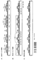
通常,時間階調を利用した駆動方法では,各ビット毎にアドレス(書き込み)期間とサステイン(点灯)期間とを設ける必要がある。アドレス(書き込み)期間とサステイン(点灯)期間とが完全に分離した駆動方法(各サブフレーム期間において、1画面分のアドレス(書き込み)期間が完全に終了してからサステイン(点灯)期間に入る方法)では,1フレーム期間内でアドレス(書き込み)期間の占める割合が大きくなり,またアドレス(書き込み)期間内でも、ある行のゲート信号線が選択されている期間は、図15(A)に示すように、他の行は書き込みも点灯も行われない状態にある期間1501が生ずるため、デューティー比(1フレーム期間内におけるサステイン(点灯)期間の長さの割合)が大きく低下する。アドレス(書き込み)期間を短くするには動作クロックを上げる以外になく、回路の動作マージン等を考えると、多階調化には限界がある。対して、アドレス(書き込み)期間とサステイン(点灯)期間とを分離しない駆動方法では、たとえばk行目のゲート信号線選択期間の終了後、直ちにk行目のEL素子はサステイン(点灯)期間に入るため、他の行のゲート信号線選択期間の間にも、いずれかの画素は点灯していることになる。よって、よりデューティー比を高くするのには有利な駆動方法といえる。
Usually, in a driving method using time gray scale, it is necessary to provide an address (writing) period and a sustain (lighting) period for each bit. Driving method in which the address (writing) period and the sustain (lighting) period are completely separated (in each subframe period, after the address (writing) period for one screen is completely completed, the sustain (lighting) period is entered. In FIG. 15A, the proportion of the address (write) period in one frame period increases, and the period in which a gate signal line in a row is selected also in the address (write) period is shown in FIG. As described above, since the
しかし、アドレス(書き込み)期間とサステイン(点灯)期間とが分離していない場合、以下のような問題が生ずる。1つのアドレス(書き込み)期間の長さは、1行目のゲート信号線選択期間の開始から、最終行のゲート信号線選択期間の終了までである。ある時点では、異なる2つのゲート信号線の選択は行うことが出来ないため、アドレス(書き込み)期間とサステイン(点灯)期間とが分離していない駆動方法においては、サステイン(点灯)期間は、少なくともアドレス(書き込み)期間と同じ(正確には、『ゲート信号線1行目にて信号の書き込みが終了してから最終行での信号の書き込みが終了するまで』の長さ)かそれ以上の長さを必要とする。よって、多階調化を図る際には、サステイン(点灯)期間の最小単位が限られてしまう。図15(B)において、最小ビット分のサブフレーム期間SF4でのアドレス(書き込み)期間Ta4が終了するまでの期間と、次のフレーム期間での最初のアドレス(書き込み)期間が開始してからの期間が重複しないだけの、1502で示される部分の長さが、この最小単位となり、これよりも短いサステイン(点灯)期間を有する場合は、正常に表示を行うことが出来ない。よって、デジタル階調方式と時間階調方式を組み合わせた場合、サステイン(点灯)期間は2のべき乗の比をもって長さが決まることから、1フレーム期間の長さを考えると、多階調化が困難になる。 However, when the address (writing) period and the sustain (lighting) period are not separated, the following problems occur. The length of one address (write) period is from the start of the gate signal line selection period of the first row to the end of the gate signal line selection period of the last row. Since two different gate signal lines cannot be selected at a certain point in time, in the driving method in which the address (writing) period and the sustain (lighting) period are not separated, the sustain (lighting) period is at least Same as the address (write) period (exactly, the length from the end of signal writing on the first row of the gate signal line until the end of signal writing on the last row) or longer Need Therefore, when increasing the number of gradations, the minimum unit of the sustain (lighting) period is limited. In FIG. 15B, the period until the address (write) period Ta 4 in the subframe period SF 4 for the minimum bit and the first address (write) period in the next frame period start. The length of the portion indicated by 1502 that does not overlap the period from is the minimum unit, and if it has a sustain (lighting) period shorter than this, display cannot be performed normally. Therefore, when the digital gray scale method and the time gray scale method are combined, the length of the sustain (lighting) period is determined by a power-of-two ratio. Therefore, considering the length of one frame period, multi-gradation is possible. It becomes difficult.
本発明は、主にデジタル階調と時間階調とを組み合わせた駆動方法において、高いデューティー比を確保し、かつアドレス(書き込み)期間よりも短いサステイン(点灯)期間を有する場合にも正常に画像(映像)の表示を可能とする新規の駆動方法を提供することを課題とする。 According to the present invention, in a driving method in which mainly digital gradation and time gradation are combined, a high duty ratio is ensured and even when a sustain (lighting) period shorter than an address (writing) period is provided, an image is normally displayed. It is an object of the present invention to provide a novel driving method capable of displaying (video).
上述した課題を解決するために、本発明においては以下の手段を講じた。 In order to solve the above-described problems, the following measures are taken in the present invention.
本発明の電子装置の駆動方法は、アドレス(書き込み)期間よりも短いサステイン(点灯)期間を有するサブフレーム期間において、サステイン(点灯)期間の終了後、次のサブフレーム期間のアドレス(書き込み)期間が開始されるまでの期間、強制的にEL素子の非表示期間を設けてアドレス(書き込み)期間の重複を回避することにより、サステイン(点灯)期間の長さを、アドレス(書き込み)期間の長さとは無関係に設定することを可能とする。これにより、多階調化によって下位ビットのサステイン(点灯)期間が短くなった場合にも、アドレス(書き込み)期間の重複を回避し、正常な画像(映像)に表示が可能となる。 According to the electronic device driving method of the present invention, in the subframe period having a sustain (lighting) period shorter than the address (writing) period, the address (writing) period of the next subframe period after the end of the sustain (lighting) period. Forcibly, the non-display period of the EL element is provided for avoiding duplication of the address (writing) period so that the length of the sustain (lighting) period is reduced to the length of the address (writing) period. It can be set regardless of the setting. As a result, even when the sustain (lighting) period of the lower bits is shortened due to the multi-gradation, duplication of the address (writing) period can be avoided and a normal image (video) can be displayed.
以下に、本発明の電子装置の構成について記載する。 The configuration of the electronic device of the present invention will be described below.
請求項1に記載の本発明の電子装置の駆動方法は、
1フレーム期間はn個のサブフレーム期間SF1、SF2、・・・、SFnを有し、
前記n個のサブフレーム期間はそれぞれアドレス(書き込み)期間Ta1、Ta2、・・・、Tanと、サステイン(点灯)期間Ts1、Ts2、・・・Tsnとを有する電子装置の駆動方法において、
前記n個のサブフレーム期間のうち少なくとも1個のサブフレーム期間において、前記アドレス(書き込み)期間と前記サステイン(点灯)期間が重複している期間を有し、
サブフレーム期間SFm(1≦m≦n)でのアドレス(書き込み)期間Tamと、サブフレーム期間SFm+1でのアドレス(書き込み)期間Tam+1とが重複する場合に、前記サブフレーム期間SFmでのサステイン(点灯)期間SFmの終了後、前記アドレス(書き込み)期間Tam+1の開始までの期間にクリア期間Tcmを有することを特徴としている。
According to a first aspect of the present invention, there is provided a driving method for an electronic device according to the present invention.
One frame period has n subframe periods SF 1 , SF 2 ,..., SF n ,
The n subframe periods each address (writing) period Ta 1, Ta 2, ···, and Ta n, a sustain (lighting) periods Ts 1, Ts 2, the electronic device having a · · · Ts n In the driving method,
At least one subframe period among the n subframe periods includes a period in which the address (writing) period and the sustain (lighting) period overlap each other,
If the address (writing) period Ta m in the sub-frame period SF m (1 ≦ m ≦ n ), an address (writing) period Ta m + 1 in the sub-frame period SF m + 1 overlap, the sub after the completion of the sustain (lighting) period SF m of the frame period SF m, it is characterized by having a clear period Tc m in the period leading up to the start of the address (writing) period Ta m + 1.
請求項2に記載の本発明の電子装置の駆動方法は、
1フレーム期間はn個のサブフレーム期間SF1、SF2、・・・、SFnを有し、
前記n個のサブフレーム期間はそれぞれアドレス(書き込み)期間Ta1、Ta2、・・・、Tanと、サステイン(点灯)期間Ts1、Ts2、・・・Tsnとを有する電子装置の駆動方法において、
前記n個のサブフレーム期間のうち少なくとも1個のサブフレーム期間において、前記アドレス(書き込み)期間と前記サステイン(点灯)期間が重複している期間を有し、
j(0<j)フレーム目のサブフレーム期間SFnでのアドレス(書き込み)期間Tanと、j+1フレーム目のサブフレーム期間SF1でのアドレス(書き込み)期間Ta1とが重複する場合に、jフレーム目のサブフレーム期間SFnでのサステイン(点灯)期間SFnの終了後、前記j+1フレーム目のサブフレーム期間SF1でのアドレス(書き込み)期間Ta1の開始までの期間にクリア期間Tcnを有することを特徴としている。
According to a second aspect of the present invention, there is provided a driving method for an electronic device according to the present invention.
One frame period has n subframe periods SF 1 , SF 2 ,..., SF n ,
The n subframe periods each address (writing) period Ta 1, Ta 2, ···, and Ta n, a sustain (lighting) periods Ts 1, Ts 2, the electronic device having a · · · Ts n In the driving method,
At least one subframe period among the n subframe periods includes a period in which the address (writing) period and the sustain (lighting) period overlap each other,
when j and address (writing) period Ta n in the subframe period SF n of (0 <j) th frame, and the address (writing) period Ta 1 in the j + 1 th frame of the sub-frame periods SF 1 overlap, after the completion of the sustain (lighting) period SF n in j-th frame of the sub-frame period SF n, the j + 1 period to the clear period to the start address (writing) period Ta 1 in the frame of the subframe periods SF 1 Tc It is characterized by having n .
請求項3に記載の本発明の電子装置の駆動方法は、
1フレーム期間はn個のサブフレーム期間SF1、SF2、・・・、SFnを有し、
前記n個のサブフレーム期間はそれぞれアドレス(書き込み)期間Ta1、Ta2、・・・、Tanと、サステイン(点灯)期間Ts1、Ts2、・・・Tsnとを有する電子装置の駆動方法において、
あるサブフレーム期間SFk(1≦k≦n)において、アドレス(書き込み)期間の長さをtak、サステイン(点灯)期間の長さをtsk、1ゲート信号線選択期間の長さをtg(tak、tsk、tg>0)として、tak>tskが成立するとき、
SFkの有するクリア期間の長さをtck(tck>0)とすると、
常に、tck≧tak−(tsk+tg)が成立することを特徴としている。
According to a third aspect of the present invention, there is provided a driving method for an electronic device according to the present invention.
One frame period has n subframe periods SF 1 , SF 2 ,..., SF n ,
The n subframe periods each address (writing) period Ta 1, Ta 2, ···, and Ta n, a sustain (lighting) periods Ts 1, Ts 2, the electronic device having a · · · Ts n In the driving method,
In a certain subframe period SF k (1 ≦ k ≦ n), the length of the address (writing) period is ta k , the length of the sustain (lighting) period is ts k , and the length of the one gate signal line selection period is t g (ta k , ts k , t g > 0) and when ta k > ts k holds,
If the length of the clear period of SF k is tc k (tc k > 0),
A feature is that tc k ≧ ta k − (ts k + t g ) always holds.
請求項4に記載の本発明の電子装置の駆動方法は、
請求項1乃至請求項3のいずれか1項に記載の電子装置の駆動方法において、
前記クリア期間において入力されるクリア信号は、保持容量線駆動回路からの信号の入力によって、保持容量線の電位を上げる、もしくは保持容量線の電位を下げることによって与えられることを特徴としている。
According to a fourth aspect of the present invention, there is provided a driving method for an electronic device according to the present invention.
The method for driving an electronic device according to any one of
The clear signal input in the clear period is given by raising the potential of the storage capacitor line or lowering the potential of the storage capacitor line by inputting a signal from the storage capacitor line driving circuit.
請求項5に記載の本発明の電子装置の駆動方法は、
請求項4に記載の電子装置の駆動方法において、
前記クリア期間中は、画像信号に関わらずEL素子が消灯することを特徴としている。
According to a fifth aspect of the present invention, there is provided a driving method for an electronic device according to the present invention.
The method for driving an electronic device according to claim 4,
During the clear period, the EL element is turned off regardless of the image signal.
請求項6に記載の本発明の電子装置は、
ソース信号線側駆動回路と、ゲート信号線側駆動回路と、保持容量線駆動回路と、画素部とを有し、
前記画素部は、複数のソース信号線と、複数のゲート信号線と、複数の電流供給線と、複数の保持容量線と、複数の画素とを有し、
前記複数の画素はそれぞれ、スイッチング用トランジスタと、EL駆動用トランジスタと、リセット用トランジスタと、保持容量と、EL素子とを有し、
前記スイッチング用トランジスタのゲート電極は、ゲート信号線と電気的に接続され、
前記スイッチング用トランジスタのソース領域とドレイン領域は、一方はソース信号線と電気的に接続され、残る一方は前記EL駆動用トランジスタのゲート電極と電気的に接続され、
前記リセット用トランジスタのゲート電極は、保持容量線と電気的に接続され、
前記リセット用トランジスタのソース領域とドレイン領域は、一方は前記ゲート信号線と電気的に接続され、残る一方は前記EL駆動用トランジスタのゲート電極と電気的に接続され、
前記保持容量は、一方の電極は前記電流供給線と電気的に接続され、残る一方の電極は前記EL駆動用トランジスタのゲート電極と電気的に接続され、
前記EL駆動用トランジスタのソース領域とドレイン領域は、一方は電流供給線と電気的に接続され、残る一方は、前記EL素子の一方の電極と電気的に接続されていることを特徴としている。
An electronic device according to a sixth aspect of the present invention includes:
A source signal line side drive circuit, a gate signal line side drive circuit, a storage capacitor line drive circuit, and a pixel portion;
The pixel portion includes a plurality of source signal lines, a plurality of gate signal lines, a plurality of current supply lines, a plurality of storage capacitor lines, and a plurality of pixels.
Each of the plurality of pixels includes a switching transistor, an EL drive transistor, a reset transistor, a storage capacitor, and an EL element.
A gate electrode of the switching transistor is electrically connected to a gate signal line;
One of a source region and a drain region of the switching transistor is electrically connected to a source signal line, and the other is electrically connected to a gate electrode of the EL driving transistor,
A gate electrode of the reset transistor is electrically connected to a storage capacitor line;
One of the source region and the drain region of the reset transistor is electrically connected to the gate signal line, and the other is electrically connected to the gate electrode of the EL driving transistor,
The storage capacitor has one electrode electrically connected to the current supply line, and the other electrode electrically connected to the gate electrode of the EL driving transistor,
One of a source region and a drain region of the EL driving transistor is electrically connected to a current supply line, and the other is electrically connected to one electrode of the EL element.
請求項7に記載の本発明の電子装置は、
請求項6に記載の電子装置において、
前記保持容量線は、前記保持容量線駆動回路と電気的に接続され、前記保持容量線駆動回路から、振幅を持った信号が入力されることを特徴としている。
An electronic device according to a seventh aspect of the present invention includes:
The electronic device according to claim 6.
The storage capacitor line is electrically connected to the storage capacitor line driving circuit, and a signal having an amplitude is input from the storage capacitor line driving circuit.
請求項8に記載の本発明の電子装置は、
1フレーム期間はn個のサブフレーム期間SF1、SF2、・・・、SFnを有し、
前記n個のサブフレーム期間はそれぞれアドレス(書き込み)期間Ta1、Ta2、・・・、Tanと、サステイン(点灯)期間Ts1、Ts2、・・・Tsnとを有し、
前記n個のサブフレーム期間のうち少なくとも1個のサブフレーム期間において、前記アドレス(書き込み)期間と前記サステイン(点灯)期間が重複している期間を有し、
サブフレーム期間SFm(1≦m≦n)でのアドレス(書き込み)期間Tamと、サブフレーム期間SFm+1でのアドレス(書き込み)期間Tam+1とが重複する場合に、前記サブフレーム期間SFmでのサステイン(点灯)期間SFmの終了後、前記アドレス(書き込み)期間Tam+1の開始までの期間にクリア期間Tcmを有する駆動方法によって動作することを特徴としている。
The electronic device of the present invention according to claim 8 is a
One frame period has n subframe periods SF 1 , SF 2 ,..., SF n ,
The n subframe periods each address (writing) period Ta 1, Ta 2, a ..., and Ta n, a sustain (lighting) periods Ts 1, Ts 2, and ... Ts n,
At least one subframe period among the n subframe periods includes a period in which the address (writing) period and the sustain (lighting) period overlap each other,
If the address (writing) period Ta m in the sub-frame period SF m (1 ≦ m ≦ n ), an address (writing) period Ta m + 1 in the sub-frame period SF m + 1 overlap, the sub after the completion of the sustain (lighting) period SF m of the frame period SF m, it is characterized by operating by a driving method having a clear period Tc m in the period leading up to the start of the address (writing) period Ta m + 1.
請求項9に記載の本発明の電子装置は、
1フレーム期間はn個のサブフレーム期間SF1、SF2、・・・、SFnを有し、
前記n個のサブフレーム期間はそれぞれアドレス(書き込み)期間Ta1、Ta2、・・・、Tanと、サステイン(点灯)期間Ts1、Ts2、・・・Tsnとを有し、
前記n個のサブフレーム期間のうち少なくとも1個のサブフレーム期間において、前記アドレス(書き込み)期間と前記サステイン(点灯)期間が重複している期間を有し、
j(0<j)フレーム目のサブフレーム期間SFnでのアドレス(書き込み)期間Tanと、j+1フレーム目のサブフレーム期間SF1でのアドレス(書き込み)期間Ta1とが重複する場合に、jフレーム目のサブフレーム期間SFnでのサステイン(点灯)期間SFnの終了後、前記j+1フレーム目のサブフレーム期間SF1でのアドレス(書き込み)期間Ta1の開始までの期間にクリア期間Tcnを有する駆動方法によって動作することを特徴している。
An electronic device according to a ninth aspect of the present invention provides:
One frame period has n subframe periods SF 1 , SF 2 ,..., SF n ,
The n subframe periods each address (writing) period Ta 1, Ta 2, a ..., and Ta n, a sustain (lighting) periods Ts 1, Ts 2, and ... Ts n,
At least one subframe period among the n subframe periods includes a period in which the address (writing) period and the sustain (lighting) period overlap each other,
when j and address (writing) period Ta n in the subframe period SF n of (0 <j) th frame, and the address (writing) period Ta 1 in the j + 1 th frame of the sub-frame periods SF 1 overlap, after completion of the sustain (lighting) period SF n in j-th frame of the sub-frame period SF n, the j + 1 period to the clear period to the start address (writing) period Ta 1 in the frame of the subframe periods SF 1 Tc It is characterized by operating by a driving method having n .
請求項10に記載の本発明の電子装置は、
1フレーム期間はn個のサブフレーム期間SF1、SF2、・・・、SFnを有し、
前記n個のサブフレーム期間はそれぞれアドレス(書き込み)期間Ta1、Ta2、・・・、Tanと、サステイン(点灯)期間Ts1、Ts2、・・・Tsnとを有し、
あるサブフレーム期間SFk(1≦k≦n)において、アドレス(書き込み)期間の長さをtak、サステイン(点灯)期間の長さをtsk、1ゲート信号線選択期間の長さをtg(tak、tsk、tg>0)として、tak>tskが成立するとき、
SFkの有するクリア期間の長さをtck(tck>0)とすると、
常に、tck≧tak−(tsk+tg)が成立することを特徴としている。
An electronic device according to a tenth aspect of the present invention includes:
One frame period has n subframe periods SF 1 , SF 2 ,..., SF n ,
The n subframe periods each address (writing) period Ta 1, Ta 2, a ..., and Ta n, a sustain (lighting) periods Ts 1, Ts 2, and ... Ts n,
In a certain subframe period SF k (1 ≦ k ≦ n), the length of the address (writing) period is ta k , the length of the sustain (lighting) period is ts k , and the length of the one gate signal line selection period is t g (ta k , ts k , t g > 0) and when ta k > ts k holds,
If the length of the clear period of SF k is tc k (tc k > 0),
A feature is that tc k ≧ ta k − (ts k + t g ) always holds.
請求項11に記載の本発明の電子装置は、
請求項8乃至請求項10のいずれか1項に記載の電子装置において、
前記クリア期間において入力されるクリア信号は、保持容量線駆動回路からの信号の入力によって、保持容量線の電位を上げる、もしくは保持容量線の電位を下げることによって与えられることを特徴としている。
The electronic device of the present invention according to claim 11 is provided.
The electronic device according to any one of claims 8 to 10,
The clear signal input in the clear period is given by raising the potential of the storage capacitor line or lowering the potential of the storage capacitor line by inputting a signal from the storage capacitor line driving circuit.
請求項12に記載の本発明の電子装置は、
請求項11に記載の電子装置において、
前記クリア期間中は、画像信号に関わらずEL素子が消灯することを特徴としている。
An electronic device according to a twelfth aspect of the present invention includes:
The electronic device according to claim 11.
During the clear period, the EL element is turned off regardless of the image signal.
本発明の効果について述べる。まず、本発明では、ある行の画素に信号を入力している期間にも、別の行の画素を非表示状態にすることが出来る。それにより、各々の行の画素において、アドレス(書き込み)期間よりも短いサステイン(点灯)期間でも自由に設定することが出来るため、多階調化が可能となる。 The effect of the present invention will be described. First, in the present invention, pixels in another row can be in a non-display state even during a period in which a signal is input to the pixels in one row. As a result, the pixels in each row can be freely set even in the sustain (lighting) period shorter than the address (writing) period, so that multi-gradation is possible.
また、本発明の駆動方法においては、EL素子を非表示にする操作は、保持容量線の電位を変化させることにより行われるので、陰極配線には、常に一定の電位が与えられる。従来のようにパルス状の信号ではないため、陰極線の電圧波形のなまりによって生じる様々な問題点を回避することが出来る。 Further, in the driving method of the present invention, the operation of hiding the EL element is performed by changing the potential of the storage capacitor line, so that a constant potential is always applied to the cathode wiring. Since it is not a pulse signal as in the prior art, various problems caused by the rounding of the voltage waveform of the cathode line can be avoided.
また、画素部の構成は、トランジスタや容量、配線などを新たに追加する必要がない。そのため、開口率を下げることなく、画質の向上が見込める。 In addition, it is not necessary to add a transistor, a capacitor, a wiring, or the like to the structure of the pixel portion. Therefore, improvement in image quality can be expected without reducing the aperture ratio.
本発明の構成について説明する。 The configuration of the present invention will be described.
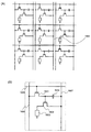
通常の画素部の構成は、図16に示すように、保持容量1604の一方の端子は、電流供給線1607に接続されており、この電流供給線は通常、一定電位に保たれている。あるいは、図17に示すように、保持容量線1711を配置して、保持容量1704の一方の端子はこの保持容量線に接続される方法もある。この場合、保持容量線1711の電位は一定に保たれている。
As shown in FIG. 16, in the normal pixel portion, one terminal of the
本発明においては、回路構成は図17に示すものを用いるので、特別な構造は必要ない。ただし、その保持容量線1711の電位は一定ではなく、回路を用いて信号を入力できるようにしている点に特徴がある。
In the present invention, since the circuit configuration shown in FIG. 17 is used, no special structure is required. However, the potential of the
アドレス(書き込み)期間およびサステイン(点灯)期間においては、この保持容量線1711の電位は一定電位に保っておく。そして、EL駆動用TFT1703のゲート電圧に関わらず、強制的に非表示期間を設ける場合には、保持容量線1711の電位を上げる。(EL駆動用TFT1702がPチャネル型の場合。Nチャネル型を用いている場合には逆の動作をする。)これを、以後はクリア信号と表記し、クリア信号が入力されている期間をクリア期間と表記する。この動作により、保持容量1704と電気的に接続されているEL駆動用TFT1702のゲート・ソース間電圧VGSも同時に引き上げられ、強制的にOFF状態となるため、この期間は、書き込まれている信号に関わらず、EL素子1703への電流の供給は停止し、クリア期間とすることが出来る。
In the address (writing) period and the sustain (lighting) period, the potential of the
なお、アドレス(書き込み)期間およびサステイン(点灯)期間において、保持容量線1711を一定電位に保つ際には、ある程度低い電位にしておくのが望ましい。これは、保持容量線を1711を一定電位に保つ期間をA期間とすると、クリア信号を入力する際には、保持容量線の電位をA期間の状態からさらに上げるため、A期間における電位が高い場合は、それよりもさらに電位を高くする必要があるためである。(EL駆動用TFT1702がPチャネル型の場合。Nチャネル型を用いている場合には逆の動作をするので、A期間では電位を高めに保つのが望ましい。)
Note that, in order to keep the
本発明の駆動方法では、保持容量線1711にクリア信号を入力することで、強制的にクリア期間を設けることが可能であるため、アドレス(書き込み)期間よりも短いサステイン(点灯)期間を設けたい場合にも、このクリア期間の長さを変えることで容易に実現出来る。よって前述の、デューティー比を高く出来る効果と相まって、多階調化に大いに有効といえる。
In the driving method of the present invention, it is possible to forcibly provide a clear period by inputting a clear signal to the
信号線から入力される信号に関係なく、EL素子1703を強制的に点灯しないようにするには、EL素子1703の陽極1709と陰極1710の間の電位差を0にする方法、EL駆動用TFT1702とEL素子1703との間に電流遮断用TFTを追加し、この電流遮断用TFTを非導通状態とすることでEL素子1703への電流供給を遮断する方法などが挙げられるが、これらの方法によると、入力する信号の波形になまり(パルスの立ち上がり時あるいは立下り時に信号遅延や鈍化が生ずる現象)が生じた場合に、各期間のタイミングにズレが生ずるため、期間が短くなるにつれて影響が大きくなる点や、追加するTFT等によって、画素の開口率が低下するといった短所もある。これに対して本発明の駆動方法では、保持容量線の電位を変えて、保持容量の電荷を開放することにより、EL素子が点灯しないようにしている。よって、この非表示区間に伴う、画像(映像)信号に関係した信号線の電位の操作は行う必要がないため、前述の信号波形のなまりが影響することはなく、TFT等を追加する必要もないので、開口率を低下させることもない。
In order not to forcibly turn on the
次に、各部の電位パターンについて説明する。図18を参照する。また、回路は引き続き図17を参照する。 Next, the potential pattern of each part will be described. Please refer to FIG. The circuit continues to refer to FIG.
図18において、1801はソース信号線1706の電位、1802はEL駆動用TFT1703のゲート電極の電位、1803はゲート信号線1705の電位、1804は保持容量線1711の電位を示している。なお、図18はスイッチング用TFT1701の極性がNチャネル型、EL駆動用TFT1702の極性がPチャネル型の場合を示している。まず、保持容量線1711の電位1804は、ある一定電位に保っておく。この電位は、後で引き上げる操作があるため、低めに保つのが望ましい。その後、ソース信号線1706、ゲート信号線1705には信号が入力され、各画素への書き込みが行われる。
In FIG. 18, 1801 indicates the potential of the
ここで、図18(A)は、EL駆動用TFT1702のゲート電極にLO信号が入力された場合、図18(B)は、EL駆動用TFT1702のゲート電極にHi信号が入力された場合を示している。図18(A)では、ゲート信号線1705の選択に伴い、EL駆動用TFT1702のゲート電極にLO信号が入力されて電位が下がり、導通状態となり、EL素子1703の点灯が開始する。対して、図18(B)では、ゲート信号線1705の選択に伴い、EL駆動用TFT1702のゲート電極にHi信号が入力され、非導通状態をとるので、EL素子1703は点灯しない。続いて、ゲート信号線1705の選択期間が終了し、ゲート信号線1705の電位が下がった後も、保持容量1704によってEL駆動用TFT1702のゲート電極に印加される電位が保たれ、図18(A)の場合はEL素子1703が点灯し続け、図18(B)の場合は消灯状態が続く。
Here, FIG. 18A shows a case where a LO signal is input to the gate electrode of the
次に、本発明におけるクリア期間前後での各部の動作について説明する。図18中、X−X'の点線で示されるタイミングで、保持容量線1711の電位1804を引き上げる。ここでは、保持容量線1711の電位1804の振幅は、ソース信号線1706の振幅よりも大きく取るのが望ましい。このとき、ゲート信号線1705の選択期間は終了し、スイッチング用TFT1701は既に非導通状態となっており、保持容量1704の両端子間の電圧はそのまま保存されるため、一方の端子に接続されている保持容量線1711の電位1804が上がると、もう一方の端子における電位、すなわちEL駆動用TFT1702のゲート電圧1802が上がることになる。よって、図18(A)において、X−X'の点線で示されるタイミングで、EL駆動用TFT1702のゲート電極の電位1802が上がる。これにより、EL駆動用TFT1702は非導通状態となり、EL素子1703への電流供給が停止し、消灯状態となる。図18(B)においても同様に、保持容量線1711の電位1804を上げるに伴い、EL駆動用TFT1702のゲート電極の電位1802も上がるが、この場合は非表示状態のまま、変化は無い。
Next, the operation of each part before and after the clear period in the present invention will be described. In FIG. 18, the potential 1804 of the
このような操作により、別の行の画素部で、ゲート信号線1705が選択され、ソース信号線1706から信号の書き込みが行われている期間であっても、EL素子1703を強制的に非表示状態とすることが出来る。したがって、このクリア期間の長さを変えることで、サステイン(点灯)期間を自由に設定することが出来る。
By such an operation, the
ところで、図18においては、スイッチング用TFT1701がNチャネル型の場合について説明したが、Pチャネル型を用いた場合にも問題なく正常に本発明の駆動方法での動作が可能である。以下に、図19を参照して説明する。また、回路は引き続き図17を参照する。
In FIG. 18, the switching
まず、保持容量線1711の電位1904は、ある一定に保っておく。前述の場合と同様の理由により、低めに保つのが望ましい。その後、ソース信号線1706、ゲート信号線1705には信号が入力され、各画素への書き込みが行われる。
First, the potential 1904 of the
ここで、図19(A)は、EL駆動用TFT1702のゲート電極にLO信号が入力された場合、図19(B)は、EL駆動用TFT1702のゲート電極にHi信号が入力された場合を示している。図19(A)では、ゲート信号線1705の選択に伴い、EL駆動用TFT1702のゲート電極にLO信号が入力されて電位が下がり、導通状態となり、EL素子1703の点灯が開始する。対して、図19(B)では、ゲート信号線1705の選択に伴い、EL駆動用TFT1702のゲート電極にHi信号が入力され、非導通状態をとるので、EL素子1703は点灯しない。続いて、ゲート信号線1705の選択期間が終了し、ゲート信号線1705の電位が下がった後も、保持容量によってEL駆動用TFT1702のゲート電極に印加される電位が保たれ、図19(A)の場合はEL素子1703が点灯し続け、図19(B)の場合は消灯状態が続く。
Here, FIG. 19A shows a case where the LO signal is input to the gate electrode of the
次に、本発明におけるクリア期間前後での各部の動作について説明する。図19中、Y−Y'の点線で示されるタイミングで、保持容量線1711の電位1904を引き上げる。このとき、図19(A)においては、ゲート信号線1705の選択期間が終了し、スイッチング用TFT1701は既に非導通状態となっているため、保持容量1704の両端子間の電圧はそのまま保存され、一方の端子に接続されている保持容量線1711の電位1904が上がると、同時にEL駆動用TFT1702のゲート電圧1902が上がることになる。よって、図19(A)において、Y−Y'の点線で示されるタイミングで、EL駆動用TFT1702のゲート電極の電位1902が上がる。これにより、EL駆動用TFT1702は非導通状態となり、EL素子1703への電流供給が停止し、消灯状態となる。図19(B)においては、保持容量線1711の電位を上げるのと同時に、EL駆動用TFT1702のゲート電極の電位1902も上がる。このとき、スイッチング用TFT1701のソース側の電位も高くなることになる。スイッチング用TFT1701の極性はPチャネル型であるから、ソース側電位が上がったことにより、スイッチング用TFT1701が、一時導通状態となる。そのため、スイッチング用TFT1701のソース・ドレイン間の電位が等しくなる方向に動く。すなわち、EL駆動用TFT1702のゲート電極電位1902が下がる。このとき、ゲート信号線1705の電位1903は一定であるから、EL駆動用TFT1702のゲート電極電位1902が下がると、同時にスイッチング用TFT1701のソース側電位が下がることになり、スイッチング用TFT1701のゲート・ソース間電圧が減少する方向に動く。そして、スイッチング用TFT1701のしきい値電圧を下回ると、スイッチング用TFT1701は非導通状態に戻る。スイッチング用TFT1701がPチャネル型の場合には、各部は以上のような動作をするが、いずれの場合にも、保持容量線1711の電位を上げると、EL駆動用TFT1702は非導通状態をとる。
Next, the operation of each part before and after the clear period in the present invention will be described. In FIG. 19, the potential 1904 of the
以上より、スイッチング用TFT1701の極性は、Nチャネル型であってもPチャネル型であっても、正常に動作が可能である。
As described above, the switching
なお、本実施形態においては、時間階調方式とデジタル階調方式とを組み合わせた場合を例にとって、本発明の説明を行ってきたが、さらに面積階調方式を組み合わせた場合においても、同様の方法でEL素子を非表示にすることが可能である。 In the present embodiment, the present invention has been described by taking the case of combining the time gray scale method and the digital gray scale method as an example, but the same applies to the case of further combining the area gray scale method. The EL element can be hidden by the method.
以下に本発明の実施例について記述する。 Examples of the present invention will be described below.
図20(A)に、全体の回路構成の一例を示す。中央に画素部が配置されている。点線枠2000で囲まれた1画素分の回路図を図20(B)に示す。画素部の上側には、ソース信号線側駆動回路が配置されている。画素部の左側には、ゲート信号線側駆動回路が配置されている。画素部の右側には、保持容量線駆動回路が配置されている。
FIG. 20A shows an example of the entire circuit configuration. A pixel portion is arranged in the center. A circuit diagram for one pixel surrounded by a dotted
タイミングチャートを用いて、実際の駆動方法について説明する。ここでは、デジタル階調と時間階調とを組み合わせた方法で、nビットの階調表現を行う場合において、簡単のため、n=3として、23=8階調の表現について述べる。なお、回路図は引き続き図20を参照する。 An actual driving method will be described using a timing chart. Here, for the sake of simplicity, when n-bit gradation expression is performed by a method combining digital gradation and time gradation, the expression of 2 3 = 8 gradations will be described with n = 3. For the circuit diagram, refer to FIG. 20 continuously.
図1は、そのときの各行のゲート信号線と保持容量線の電位のタイミングチャートである。本実施例にて用いる回路においては、スイッチング用TFT2001にはNチャネル型を用いている。よって、ゲート信号線選択期間においては、ゲート信号線2005の電位は高くなり、スイッチング用TFT2001が導通状態となる。
FIG. 1 is a timing chart of potentials of gate signal lines and storage capacitor lines in each row at that time. In the circuit used in this embodiment, an N-channel type is used for the switching
順を追って説明する。まず、nビットの階調を表現するためには、1フレーム期間をn個のサブフレーム期間に分割する必要がある。本実施例においては、3ビットであるから、SF1〜SF3の3つのサブフレーム期間に分割している。各サブフレーム期間はそれぞれ、アドレス(書き込み)期間Ta1〜Ta3、サステイン(点灯)期間Ts1〜Ts3を有している。アドレス(書き込み)期間は、1画面分の書き込みを行うのに要する期間であるから、全て長さは等しい。また、サステイン(点灯)期間の長さは、2のべき乗で変わるようにする。すなわち、図1の場合は、Ts1:Ts2:Ts3=4:2:1となる。 I will explain in order. First, in order to express an n-bit gradation, it is necessary to divide one frame period into n subframe periods. In this embodiment, since it is 3 bits, it is divided into three subframe periods of SF 1 to SF 3 . Each subframe period has an address (writing) period Ta 1 to Ta 3 and a sustain (lighting) period Ts 1 to Ts 3 . Since the address (writing) period is a period required for writing for one screen, the lengths are all equal. Further, the length of the sustain (lighting) period is changed to a power of 2. That is, in the case of FIG. 1, Ts 1 : Ts 2 : Ts 3 = 4: 2: 1.
ただし、必ずしもサステイン(点灯)期間の長さを2のべき乗の比としなくとも、階調表示は可能である。 However, gradation display is possible even if the length of the sustain (lighting) period is not necessarily a power-of-two ratio.
本実施例のタイミングチャートは、アドレス(書き込み)期間とサステイン(点灯)期間が完全に分離しておらず、かつアドレス(書き込み)期間よりも短いサステイン(点灯)期間を有している。まず、SF1にて、1行づつゲート信号線2005が選択され、その間に画素に信号の書き込みが行われる。1行分の書き込みが終了する(ゲート信号線選択期間が終了する)と、その行はサステイン(点灯)期間Ts1に入る。
In the timing chart of this embodiment, the address (writing) period and the sustain (lighting) period are not completely separated, and the sustain (lighting) period is shorter than the address (writing) period. First, in SF 1 , the
SF1でのサステイン(点灯)期間Ts1の終了後、SF2に入り、同様にゲート信号線2005が1行づつ選択され、画素へ信号の書き込みが行われる。この間は、保持容量線2011の電位は一定に保たれている。
After the end of the sustain (lighting) period Ts 1 in SF 1 , the process enters SF 2 , and similarly, the
その後、SF3に入る。SF3においては、図1に示すように、アドレス(書き込み)期間Ta3よりも、サステイン(点灯)期間Ts3が短い。よって、これまでのサブフレーム期間と同様、アドレス(書き込み)期間の終了後にサステイン(点灯)期間に入り、サステイン(点灯)期間の終了後に、直ちに次のサブフレーム期間に入った場合、図2(A)に示すように、SF3のアドレス(書き込み)期間Ta3が終了する前に、次のフレーム期間でのSF1のアドレス(書き込み)期間Ta1が開始するため、異なるサブフレーム期間のアドレス(書き込み)期間が重複する部分が現れる。この期間は、同時に異なる2列のゲート信号線が選択されることを意味しており、そのようなタイミングでは、正常に画像(映像)の表示を行うことは出来ない。 Then enter SF 3 . In SF 3 , as shown in FIG. 1, the sustain (lighting) period Ts 3 is shorter than the address (writing) period Ta 3 . Therefore, as in the previous subframe period, when the sustain (lighting) period is entered after the end of the address (writing) period and the next subframe period is entered immediately after the end of the sustain (lighting) period, FIG. as shown in a), before the SF 3 address (writing) period Ta 3 is terminated, the address for the address SF 1 in the next frame period (writing) period Ta 1 is started, different subframe periods A portion where the (writing) period overlaps appears. This period means that two different rows of gate signal lines are selected at the same time. At such timing, an image (video) cannot be displayed normally.
そこで、図2(B)に示すように、Ts3の終了後からの一定期間(サステイン(点灯)期間が終了した後、次のアドレス(書き込み)期間が開始されるまでの期間)に、保持容量線2011の電位を上げることで、EL素子2003が点灯しない期間を強制的に設ける。この、EL素子2003のクリア期間を、クリア期間(Tcn n:サブフレームの番号)と表記する。図2(B)において、Ts3の終了後にTc3が設けられていることで、Ta3と次のTa1の重複が回避出来るため、画像(映像)を正常に表示することが出来る。
Therefore, as shown in FIG. 2B, the data is held for a certain period from the end of Ts 3 (the period from the end of the sustain (lighting) period to the start of the next address (writing) period). By raising the potential of the
なお、このクリア期間は、あるサブフレーム期間SFk(1≦k≦n)において、アドレス(書き込み)期間Takよりも短いサステイン(点灯)期間Tskを有するときは、アドレス(書き込み)期間の長さをtak、サステイン(点灯)期間の長さをtsk、1ゲート信号線選択期間の長さをtg(tak、tsk、tg>0)として、SFkの有するクリア期間の長さをtck(tck>0)とすると、常に、tck≧tak−(tsk+tg)が成立するだけの長さを最低限必要とする。 Incidentally, the clear period, at subframe period SF k (1 ≦ k ≦ n ), when a short sustain (lighting) periods Ts k than the address (writing) period Ta k is an address (writing) period The clear period of SF k , where the length is ta k , the sustain (lighting) period is ts k , and the length of one gate signal line selection period is t g (ta k , ts k , t g > 0). When the length and tc k (tc k> 0) , always, tc k ≧ ta k - ( ts k + t g) is the minimum required length of just established.
本実施例においては、実施例1よりも階調数が多く、かつアドレス(書き込み)期間よりも短いサステイン(点灯)期間を複数有する場合の例について述べる。回路は実施例1と同様であるので、引き続き図20を参照する。 In the present embodiment, an example will be described in which there are a plurality of sustain (lighting) periods having a larger number of gradations than the first embodiment and shorter than the address (writing) period. Since the circuit is the same as that of the first embodiment, reference is continuously made to FIG.
本実施例では、5ビット(25=32)階調の表現について述べる。3ビット階調表現の場合と同様、アドレス(書き込み)期間Ta1〜Ta5は、全て同じ長さであり、サステイン(点灯)期間Ts1〜Ts5は、Ts1:Ts2:Ts3:Ts4:Ts5=16:8:4:2:1としている。うち、Ts3、Ts4、Ts5の長さは、アドレス(書き込み)期間よりも短い。 In the present embodiment, description will be given of 5 -bit (2 5 = 32) gradation expression. As in the case of 3-bit gradation expression, the address (writing) periods Ta 1 to Ta 5 are all the same length, and the sustain (lighting) periods Ts 1 to Ts 5 are Ts 1 : Ts 2 : Ts 3 : Ts 4 : Ts 5 = 16: 8: 4: 2: 1. Of these, the lengths of Ts 3 , Ts 4 , and Ts 5 are shorter than the address (write) period.
信号の書き込みが終了した後、直ちにEL素子2003の点灯が開始される駆動方法では、サステイン(点灯)期間が終了した後に、次のアドレス(書き込み)期間に入ると、図3(A)に示すように、異なるサブフレーム期間のアドレス(書き込み)期間が重複する部分が現れる。図中、aで示される範囲においては、Ta3とTa4の2つが重複し、bで示される範囲においては、Ta4とTa5の2つが重複し、cで示される範囲においては、Ta4とTa5と、次のサブフレーム期間におけるTa1(Ta1'と表記)の3つが重複し、dで示される範囲においては、Ta5とTa1'の2つが重複する。このように、階調数が増加するほど、最小単位のサステイン(点灯)期間が短くなるため、3つ以上のアドレス(書き込み)期間が重複する場合も生ずる。よって、実施例1と同様に、サステイン(点灯)期間が終了した後、次のアドレス(書き込み)期間が開始されるまでの間に、図3(B)に示すようにそれぞれクリア期間Tc3、Tc4、Tc5を設ける。これにより、アドレス(書き込み)期間の重複を回避し、正常な画像(映像)の表示が出来る。
In the driving method in which the lighting of the
本実施例においては、同一基板上に、画素部および画素部の周辺に設ける駆動回路のTFT(Nチャネル型TFTおよびPチャネル型TFT)を同時に作製する方法について詳細に説明する。 In this embodiment, a method for simultaneously manufacturing a pixel portion and TFTs (N-channel TFT and P-channel TFT) of a driver circuit provided around the pixel portion on the same substrate will be described in detail.
まず、図4(A)に示すように、コーニング社の#7059ガラスや#1737ガラスなどに代表されるバリウムホウケイ酸ガラス、またはアルミノホウケイ酸ガラスなどのガラスから成る基板5001上に酸化シリコン膜、窒化シリコン膜または酸化窒化シリコン膜などの絶縁膜から成る下地膜5002を形成する。例えば、プラズマCVD法でSiH4、NH3、N2Oから作製される酸化窒化シリコン膜5002aを10〜200[nm](好ましくは50〜100[nm])形成し、同様にSiH4、N2Oから作製される酸化窒化水素化シリコン膜5002bを50〜200[nm](好ましくは100〜150[nm])の厚さに積層形成する。本実施例では下地膜5002を2層構造として示したが、前記絶縁膜の単層膜または2層以上積層させた構造として形成しても良い。
First, as shown in FIG. 4A, a silicon oxide film is formed on a
島状半導体層5003〜5006は、非晶質構造を有する半導体膜をレーザー結晶化法や公知の熱結晶化法を用いて作製した結晶質半導体膜で形成する。この島状半導体層5003〜5006の厚さは25〜80[nm](好ましくは30〜60[nm])の厚さで形成する。結晶質半導体膜の材料に限定はないが、好ましくはシリコンまたはシリコンゲルマニウム(SiGe)合金などで形成すると良い。
The island-shaped
レーザー結晶化法で結晶質半導体膜を作製するには、パルス発振型または連続発光型のエキシマレーザーやYAGレーザー、YVO4レーザーを用いる。これらのレーザーを用いる場合には、レーザー発振器から放射されたレーザー光を光学系で線状に集光し半導体膜に照射する方法を用いると良い。結晶化の条件は実施者が適宣選択するものであるが、エキシマレーザーを用いる場合はパルス発振周波数30[Hz]とし、レーザーエネルギー密度を100〜400[mJ/cm2](代表的には200〜300[mJ/cm2])とする。また、YAGレーザーを用いる場合にはその第2高調波を用いパルス発振周波数1〜10[kHz]とし、レーザーエネルギー密度を300〜600[mJ/cm2](代表的には350〜500[mJ/cm2])とすると良い。そして幅100〜1000[μm]、例えば400[μm]で線状に集光したレーザー光を基板全面に渡って照射し、この時の線状レーザー光の重ね合わせ率(オーバーラップ率)を80〜98[%]として行う。 In order to manufacture a crystalline semiconductor film by a laser crystallization method, a pulse oscillation type or continuous emission type excimer laser, YAG laser, or YVO 4 laser is used. When these lasers are used, it is preferable to use a method in which laser light emitted from a laser oscillator is linearly collected by an optical system and irradiated onto a semiconductor film. The conditions for crystallization are appropriately selected by the practitioner. When an excimer laser is used, the pulse oscillation frequency is 30 [Hz] and the laser energy density is 100 to 400 [mJ / cm 2 ] (typically 200 to 300 [mJ / cm 2 ]). When a YAG laser is used, the second harmonic is used and the pulse oscillation frequency is 1 to 10 [kHz], and the laser energy density is 300 to 600 [mJ / cm 2 ] (typically 350 to 500 [mJ]. / cm 2 ]). Then, a laser beam condensed in a linear shape with a width of 100 to 1000 [μm], for example, 400 [μm] is irradiated over the entire surface of the substrate, and the superposition ratio (overlap ratio) of the linear laser light at this time is 80 Perform as ~ 98 [%].
次いで、島状半導体層5003〜5006を覆うゲート絶縁膜5007を形成する。ゲート絶縁膜5007はプラズマCVD法またはスパッタ法を用い、厚さを40〜150[nm]としてシリコンを含む絶縁膜で形成する。本実施例では、120[nm]の厚さで酸化窒化シリコン膜で形成する。勿論、ゲート絶縁膜はこのような酸化窒化シリコン膜に限定されるものでなく、他のシリコンを含む絶縁膜を単層または積層構造として用いても良い。例えば、酸化シリコン膜を用いる場合には、プラズマCVD法でTEOS(Tetraethyl Orthosilicate)とO2とを混合し、反応圧力40[Pa]、基板温度300〜400[℃]とし、高周波(13.56[MHz])電力密度0.5〜0.8[W/cm2]で放電させて形成することができる。このようにして作製される酸化シリコン膜は、その後400〜500[℃]の熱アニールによりゲート絶縁膜として良好な特性を得ることができる。
Next, a
そして、ゲート絶縁膜5007上にゲート電極を形成するための第1の導電膜5008と第2の導電膜5009とを形成する。本実施例では、第1の導電膜5008をTaで50〜100[nm]の厚さに形成し、第2の導電膜5009をWで100〜300[nm]の厚さに形成する。
Then, a first
Ta膜はスパッタ法で、TaのターゲットをArでスパッタすることにより形成する。この場合、Arに適量のXeやKrを加えると、Ta膜の内部応力を緩和して膜の剥離を防止することができる。また、α相のTa膜の抵抗率は20[μΩcm]程度でありゲート電極に使用することができるが、β相のTa膜の抵抗率は180[μΩcm]程度でありゲート電極とするには不向きである。α相のTa膜を形成するために、Taのα相に近い結晶構造をもつ窒化タンタルを10〜50[nm]程度の厚さでTaの下地に形成しておくとα相のTa膜を容易に得ることができる。 The Ta film is formed by sputtering, and a Ta target is sputtered with Ar. In this case, when an appropriate amount of Xe or Kr is added to Ar, the internal stress of the Ta film can be relieved and peeling of the film can be prevented. The resistivity of the α-phase Ta film is about 20 [μΩcm] and can be used for the gate electrode, but the resistivity of the β-phase Ta film is about 180 [μΩcm] and is used as the gate electrode. It is unsuitable. In order to form an α-phase Ta film, tantalum nitride having a crystal structure close to Ta's α-phase is formed on a Ta base with a thickness of about 10 to 50 nm. Can be easily obtained.
W膜を形成する場合には、Wをターゲットとしたスパッタ法で形成する。その他に6フッ化タングステン(WF6)を用いる熱CVD法で形成することもできる。いずれにしてもゲート電極として使用するためには低抵抗化を図る必要があり、W膜の抵抗率は20[μΩcm]以下にすることが望ましい。W膜は結晶粒を大きくすることで低抵抗率化を図ることができるが、W中に酸素などの不純物元素が多い場合には結晶化が阻害され高抵抗化する。このことより、スパッタ法による場合、純度99.9999[%]のWターゲットを用い、さらに成膜時に気相中からの不純物の混入がないように十分配慮してW膜を形成することにより、抵抗率9〜20[μΩcm]を実現することができる。 When forming a W film, it is formed by sputtering using W as a target. In addition, it can be formed by a thermal CVD method using tungsten hexafluoride (WF 6 ). In any case, in order to use as a gate electrode, it is necessary to reduce the resistance, and it is desirable that the resistivity of the W film be 20 [μΩcm] or less. The resistivity of the W film can be reduced by increasing the crystal grains. However, when there are many impurity elements such as oxygen in W, crystallization is hindered and the resistance is increased. From this, in the case of the sputtering method, by using a W target having a purity of 99.9999 [%] and further forming a W film with sufficient consideration so that impurities are not mixed in from the gas phase during film formation, A resistivity of 9 to 20 [μΩcm] can be realized.
なお、本実施例では、第1の導電膜5008をTa、第2の導電膜5009をWとしたが、特に限定されず、いずれもTa、W、Ti、Mo、Al、Cuから選ばれた元素、または前記元素を主成分とする合金材料もしくは化合物材料で形成してもよい。また、リン等の不純物元素をドーピングした多結晶シリコン膜に代表される半導体膜を用いてもよい。本実施例以外の他の組み合わせの一例は、第1の導電膜を窒化タンタル(TaN)で形成し、第2の導電膜をWとする組み合わせ、第1の導電膜を窒化タンタル(TaN)で形成し、第2の導電膜をAlとする組み合わせ、第1の導電膜を窒化タンタル(TaN)で形成し、第2の導電膜をCuとする組み合わせで形成することが好ましい。
Note that in this example, the first
次に、レジストによるマスク5010を形成し、電極及び配線を形成するための第1のエッチング処理を行う。本実施例ではICP(Inductively Coupled Plasma:誘導結合型プラズマ)エッチング法を用い、エッチング用ガスにCF4とCl2を混合し、1[Pa]の圧力でコイル型の電極に500[W]のRF(13.56[MHz])電力を投入してプラズマを生成して行う。基板側(試料ステージ)にも100[W]のRF(13.56[MHz])電力を投入し、実質的に負の自己バイアス電圧を印加する。CF4とCl2を混合した場合にはW膜及びTa膜とも同程度にエッチングされる。
Next, a resist
上記エッチング条件では、レジストによるマスクの形状を適したものとすることにより、基板側に印加するバイアス電圧の効果により第1の導電層及び第2の導電層の端部がテーパー形状となる。テーパー部の角度は15〜45°となる。ゲート絶縁膜上に残渣を残すことなくエッチングするためには、10〜20[%]程度の割合でエッチング時間を増加させると良い。W膜に対する酸化窒化シリコン膜の選択比は2〜4(代表的には3)であるので、オーバーエッチング処理により、酸化窒化シリコン膜が露出した面は20〜50[nm]程度エッチングされることになる。こうして、第1のエッチング処理により第1の導電層と第2の導電層から成る第1の形状の導電層5011〜5016(第1の導電層5011a〜5016aと第2の導電層5011b〜5016b)を形成する。このとき、ゲート絶縁膜5007においては、第1の形状の導電層5011〜5016で覆われない領域は20〜50[nm]程度エッチングされ薄くなった領域が形成される(図4(A))。
Under the above etching conditions, by making the shape of the resist mask suitable, the end portions of the first conductive layer and the second conductive layer are tapered due to the effect of the bias voltage applied to the substrate side. The angle of the tapered portion is 15 to 45 °. In order to perform etching without leaving a residue on the gate insulating film, it is preferable to increase the etching time at a rate of about 10 to 20%. Since the selection ratio of the silicon oxynitride film to the W film is 2 to 4 (typically 3), the surface where the silicon oxynitride film is exposed is etched by about 20 to 50 [nm] by the overetching process. become. Thus, the first shape
そして、第1のドーピング処理を行いN型を付与する不純物元素を添加する(図4(B))。ドーピングの方法はイオンドープ法もしくはイオン注入法で行えば良い。イオンドープ法の条件はドーズ量を1×10¹³〜5×10¹⁴[atoms/cm2]とし、加速電圧を60〜100[keV]として行う。N型を付与する不純物元素として15族に属する元素、典型的にはリン(P)または砒素(As)を用いるが、ここではリン(P)を用いる。この場合、導電層5011〜5015がN型を付与する不純物元素に対するマスクとなり、自己整合的に第1の不純物領域5017〜5025が形成される。第1の不純物領域5017〜5025には1×1020〜1×1021[atoms/cm3]の濃度範囲でN型を付与する不純物元素を添加する。
Then, an impurity element imparting n-type conductivity is added by performing a first doping process (FIG. 4B). As a doping method, an ion doping method or an ion implantation method may be used. The conditions of the ion doping method are a dose amount of 1 × 10 13 to 5 × 10 14 [atoms / cm 2 ] and an acceleration voltage of 60 to 100 [keV]. As an impurity element imparting N-type, an element belonging to Group 15, typically phosphorus (P) or arsenic (As) is used. Here, phosphorus (P) is used. In this case, the
次に、図4(C)に示すように第2のエッチング処理を行う。同様にICPエッチング法を用い、エッチングガスにCF4とCl2とO2を混合して、1[Pa]の圧力でコイル型の電極に500[W]のRF(13.56[MHz])電力を供給し、プラズマを生成して行う。基板側(試料ステージ)には50[W]のRF(13.56[MHz])電力を投入し、第1のエッチング処理に比べ低い自己バイアス電圧を印加する。このような条件によりW膜を異方性エッチングし、かつ、それより遅いエッチング速度で第1の導電層であるTaを異方性エッチングして第2の形状の導電層5026〜5031(第1の導電層5026a〜5031aと第2の導電層5026b〜5031b)を形成する。このとき、ゲート絶縁膜5007においては、第2の形状の導電層5026〜5031で覆われない領域はさらに20〜50[nm]程度エッチングされ薄くなった領域が形成される。
Next, a second etching process is performed as shown in FIG. Similarly, using an ICP etching method, CF 4 , Cl 2, and O 2 are mixed in an etching gas, and 500 [W] RF (13.56 [MHz]) is applied to a coil-type electrode at a pressure of 1 [Pa]. This is done by supplying power and generating plasma. 50 [W] RF (13.56 [MHz]) power is applied to the substrate side (sample stage), and a lower self-bias voltage is applied than in the first etching process. Under such conditions, the W film is anisotropically etched, and Ta, which is the first conductive layer, is anisotropically etched at a slower etching rate to form the second shape
W膜やTa膜のCF4とCl2の混合ガスによるエッチング反応は、生成されるラジカルまたはイオン種と反応生成物の蒸気圧から推測することができる。WとTaのフッ化物と塩化物の蒸気圧を比較すると、Wのフッ化物であるWF6が極端に高く、その他のWCl5、TaF5、TaCl5は同程度である。従って、CF4とCl2の混合ガスではW膜及びTa膜共にエッチングされる。しかし、この混合ガスに適量のO2を添加するとCF4とO2が反応してCOとFになり、FラジカルまたはFイオンが多量に発生する。その結果、フッ化物の蒸気圧が高いW膜のエッチング速度が増大する。一方、TaはFが増大しても相対的にエッチング速度の増加は少ない。また、TaはWに比較して酸化されやすいので、O2を添加することでTaの表面が酸化される。Taの酸化物はフッ素や塩素と反応しないためさらにTa膜のエッチング速度は低下する。従って、W膜とTa膜とのエッチング速度に差を作ることが可能となりW膜のエッチング速度をTa膜よりも大きくすることが可能となる。 The etching reaction of the W film or Ta film with the mixed gas of CF 4 and Cl 2 can be estimated from the generated radical or ion species and the vapor pressure of the reaction product. When the vapor pressures of W and Ta fluorides and chlorides are compared, WF 6 which is a fluoride of W is extremely high, and other WCl 5 , TaF 5 and TaCl 5 are similar. Therefore, both the W film and the Ta film are etched with a mixed gas of CF 4 and Cl 2 . However, when an appropriate amount of O 2 is added to this mixed gas, CF 4 and O 2 react to form CO and F, and a large amount of F radicals or F ions are generated. As a result, the etching rate of the W film having a high fluoride vapor pressure is increased. On the other hand, the increase in etching rate of Ta is relatively small even when F increases. Further, since Ta is more easily oxidized than W, the surface of Ta is oxidized by adding O 2 . Since the Ta oxide does not react with fluorine or chlorine, the etching rate of the Ta film further decreases. Therefore, it is possible to make a difference in the etching rate between the W film and the Ta film, and the etching rate of the W film can be made larger than that of the Ta film.
そして、図5(A)に示すように第2のドーピング処理を行う。この場合、第1のドーピング処理よりもドーズ量を下げて高い加速電圧の条件としてN型を付与する不純物元素をドーピングする。例えば、加速電圧を70〜120[keV]とし、1×10¹³[atoms/cm2]のドーズ量で行い、図4(B)で島状半導体層に形成された第1の不純物領域の内側に新たな不純物領域を形成する。ドーピングは、第2の形状の導電層5026〜5030を不純物元素に対するマスクとして用い、第2の導電層5026a〜5030aの下側の領域にも不純物元素が添加されるようにドーピングする。こうして、第2の導電層5026a〜5030aと重なる第3の不純物領域5032〜5041と、第1の不純物領域と第3の不純物領域との間の第2の不純物領域5042〜5051とを形成する。N型を付与する不純物元素は、第2の不純物領域で1×1017〜1×1019[atoms/cm3]の濃度となるようにし、第3の不純物領域で1×1016〜1×1018[atoms/cm3]の濃度となるようにする。
Then, a second doping process is performed as shown in FIG. In this case, the impurity amount imparting N-type is doped as a condition of a high acceleration voltage by lowering the dose than the first doping treatment. For example, the acceleration voltage is set to 70 to 120 [keV] and the dose is 1 × 10 13 [atoms / cm 2 ], and the inside of the first impurity region formed in the island-shaped semiconductor layer in FIG. Then, a new impurity region is formed. Doping is performed using the second shape
そして、図5(B)に示すように、Pチャネル型TFTを形成する島状半導体層5004、5006に第1の導電型とは逆の導電型の第4の不純物領域5052〜5063を形成する。第2の導電層5027b、5030bを不純物元素に対するマスクとして用い、自己整合的に不純物領域を形成する。このとき、Nチャネル型TFTを形成する島状半導体層5003、5005はレジストマスク5200で全面を被覆しておく。不純物領域5052〜5063にはそれぞれ異なる濃度でリンが添加されているが、ジボラン(B2H6)を用いたイオンドープ法で形成し、そのいずれの領域においても不純物濃度を2×10²⁰〜2×10²¹[atoms/cm3]となるようにする。
Then, as shown in FIG. 5B,
以上までの工程でそれぞれの島状半導体層に不純物領域が形成される。島状半導体層と重なる第2の導電層5026〜5030がゲート電極として機能する。また、5031は島状のソース信号線として機能する。
Through the above steps, impurity regions are formed in each island-like semiconductor layer. Second
こうして導電型の制御を目的として図5(C)に示すように、それぞれの島状半導体層に添加された不純物元素を活性化する工程を行う。この工程はファーネスアニール炉を用いる熱アニール法で行う。その他に、レーザーアニール法、またはラピッドサーマルアニール法(RTA法)を適用することができる。熱アニール法では酸素濃度が1[ppm]以下、好ましくは0.1[ppm]以下の窒素雰囲気中で400〜700[℃]、代表的には500〜600[℃]で行うものであり、本実施例では500[℃]で4時間の熱処理を行う。ただし、5026〜5031に用いた配線材料が熱に弱い場合には、配線等を保護するため層間絶縁膜(シリコンを主成分とする)を形成した後で活性化を行うことが好ましい。 Thus, for the purpose of controlling the conductivity type, as shown in FIG. 5C, a step of activating the impurity element added to each island-like semiconductor layer is performed. This step is performed by a thermal annealing method using a furnace annealing furnace. In addition, a laser annealing method or a rapid thermal annealing method (RTA method) can be applied. In the thermal annealing method, oxygen concentration is 1 [ppm] or less, preferably 0.1 [ppm] or less in a nitrogen atmosphere at 400 to 700 [° C.], typically 500 to 600 [° C.], In this embodiment, heat treatment is performed at 500 [° C.] for 4 hours. However, when the wiring material used for 5026 to 5031 is weak against heat, activation is preferably performed after an interlayer insulating film (mainly composed of silicon) is formed in order to protect the wiring and the like.
さらに、3〜100[%]の水素を含む雰囲気中で、300〜450[℃]で1〜12時間の熱処理を行い、島状半導体層を水素化する工程を行う。この工程は熱的に励起された水素により半導体層のダングリングボンドを終端する工程である。水素化の他の手段として、プラズマ水素化(プラズマにより励起された水素を用いる)を行っても良い。 Further, a heat treatment is performed at 300 to 450 [° C.] for 1 to 12 hours in an atmosphere containing 3 to 100 [%] hydrogen to perform a step of hydrogenating the island-shaped semiconductor layer. This step is a step of terminating dangling bonds in the semiconductor layer with thermally excited hydrogen. As another means of hydrogenation, plasma hydrogenation (using hydrogen excited by plasma) may be performed.
次いで、図6(A)に示すように、第1の層間絶縁膜5064を酸化窒化シリコン膜から100〜200[nm]の厚さで形成する。その上に有機絶縁物材料から成る第2の層間絶縁膜5065を形成した後、第1の層間絶縁膜5064、第2の層間絶縁膜5065、およびゲート絶縁膜5007に対してコンタクトホールを形成し、各配線(接続配線、信号線を含む)5066〜5071、5073をパターニング形成した後、接続配線5071に接する画素電極5072をパターニング形成する。
Next, as shown in FIG. 6A, a first
第2の層間絶縁膜5065としては、有機樹脂を材料とする膜を用い、その有機樹脂としてはポリイミド、ポリアミド、アクリル、BCB(ベンゾシクロブテン)等を使用することが出来る。特に、第2の層間絶縁膜5065は平坦化の意味合いが強いので、平坦性に優れたアクリルが好ましい。本実施例ではTFTによって形成される段差を十分に平坦化しうる膜厚でアクリル膜を形成する。好ましくは1〜5[μm](さらに好ましくは2〜4[μm])とすれば良い。
As the second
コンタクトホールの形成は、ドライエッチングまたはウエットエッチングを用い、N型の不純物領域5017〜5021および5023〜5025またはP型の不純物領域5052〜5063に達するコンタクトホール、配線5031に達するコンタクトホール、電流供給線に達するコンタクトホール(図示せず)、およびゲート電極に達するコンタクトホール(図示せず)をそれぞれ形成する。
The contact hole is formed by dry etching or wet etching. The contact hole reaches the N-
また、配線(接続配線、信号線を含む)5066〜5071、5073として、Ti膜を100[nm]、Tiを含むアルミニウム膜を300[nm]、Ti膜150[nm]をスパッタ法で連続形成した3層構造の積層膜を所望の形状にパターニングしたものを用いる。勿論、他の導電膜を用いても良い。 Further, as wirings (including connection wirings and signal lines) 5066 to 5071 and 5073, a Ti film is 100 nm, an aluminum film containing Ti is 300 nm, and a Ti film 150 nm is continuously formed by sputtering. A film obtained by patterning the laminated film having the three-layer structure into a desired shape is used. Of course, other conductive films may be used.
また、本実施例では、画素電極5072としてITO膜を110[nm]の厚さに形成し、パターニングを行った。画素電極5072を接続配線5071と接して重なるように配置することでコンタクトを取っている。また、酸化インジウムに2〜20[%]の酸化亜鉛(ZnO)を混合した透明導電膜を用いても良い。この画素電極5072がEL素子の陽極となる(図6(A))。
In this embodiment, an ITO film having a thickness of 110 [nm] is formed as the
次に、図6(B)に示すように、珪素を含む絶縁膜(本実施例では酸化珪素膜)を500[nm]の厚さに形成し、画素電極5072に対応する位置に開口部を形成して第3の層間絶縁膜5074を形成する。開口部を形成する際、ウエットエッチング法を用いることで容易にテーパー形状の側壁とすることが出来る。開口部の側壁が十分になだらかでないと段差に起因するEL層の劣化が顕著な問題となってしまう。
Next, as shown in FIG. 6B, an insulating film containing silicon (silicon oxide film in this embodiment) is formed to a thickness of 500 [nm], and an opening is formed at a position corresponding to the
次に、EL層5075および陰極(MgAg電極)5076を、真空蒸着法を用いて大気解放しないで連続形成する。なお、EL層5075の膜厚は80〜200[nm](典型的には100〜120[nm])、陰極5076の厚さは180〜300[nm](典型的には200〜250[nm])とすれば良い。
Next, the
この工程では、赤色に対応する画素、緑色に対応する画素および青色に対応する画素に対して順次、EL層および陰極を形成する。但し、EL層は溶液に対する耐性に乏しいためフォトリソグラフィ技術を用いずに各色個別に形成しなくてはならない。そこでメタルマスクを用いて所望の画素以外を隠し、必要箇所だけ選択的にEL層および陰極を形成するのが好ましい。 In this step, an EL layer and a cathode are sequentially formed for a pixel corresponding to red, a pixel corresponding to green, and a pixel corresponding to blue. However, since the EL layer has poor resistance to the solution, it has to be formed individually for each color without using a photolithography technique. Therefore, it is preferable to hide other than the desired pixels using a metal mask, and selectively form the EL layer and the cathode only at necessary portions.
即ち、まず赤色に対応する画素以外を全て隠すマスクをセットし、そのマスクを用いて赤色発光のEL層および陰極を選択的に形成する。次いで、緑色に対応する画素以外を全て隠すマスクをセットし、そのマスクを用いて緑色発光のEL層および陰極を選択的に形成する。次いで、同様に青色に対応する画素以外を全て隠すマスクをセットし、そのマスクを用いて青色発光のEL層および陰極を選択的に形成する。なお、ここでは全て異なるマスクを用いるように記載しているが、同じマスクを使いまわしても構わない。また、全画素にEL層および陰極を形成するまで真空を破らずに処理することが好ましい。 That is, first, a mask that hides all pixels other than those corresponding to red is set, and the EL layer and the cathode emitting red light are selectively formed using the mask. Next, a mask for hiding all but the pixels corresponding to green is set, and a green light emitting EL layer and a cathode are selectively formed using the mask. Next, similarly, a mask for hiding all but the pixels corresponding to blue is set, and an EL layer and a cathode emitting blue light are selectively formed using the mask. Note that although all the different masks are described here, the same mask may be used. Further, it is preferable to perform processing without breaking the vacuum until the EL layer and the cathode are formed on all the pixels.
ここではRGBに対応した3種類のEL素子を形成する方式を用いたが、白色発光のEL素子とカラーフィルタを組み合わせた方式、青色または青緑発光のEL素子と蛍光体(蛍光性の色変換層:CCM)とを組み合わせた方式、陰極(対向電極)に透明電極を利用してRGBに対応したEL素子を重ねる方式などを用いても良い。 Here, a method of forming three types of EL elements corresponding to RGB is used, but a method of combining a white light emitting EL element and a color filter, a blue or blue green light emitting EL element, and a phosphor (fluorescent color conversion). Layer: CCM), a method of superimposing EL elements corresponding to RGB by using a transparent electrode as a cathode (counter electrode), or the like may be used.
なお、EL層5075としては公知の材料を用いることが出来る。公知の材料としては、駆動電圧を考慮すると有機材料を用いるのが好ましい。例えば正孔注入層、正孔輸送層、発光層および電子注入層でなる4層構造をEL層とすれば良い。また、本実施例ではEL素子の陰極としてMgAg電極を用いた例を示すが、公知の他の材料であっても良い。
Note that a known material can be used for the
次いで、EL層および陰極を覆って保護電極5077を形成する。この保護電極5077としてはアルミニウムを主成分とする導電膜を用いれば良い。保護電極5077はEL層および陰極を形成した時とは異なるマスクを用いて真空蒸着法で形成すれば良い。また、EL層および陰極を形成した後で大気解放しないで連続的に形成することが好ましい。
Next, a
最後に、窒化珪素膜でなるパッシベーション膜5078を300[nm]の厚さに形成する。実際には保護電極5088がEL層を水分等から保護する役割を果たすが、さらにパッシベーション膜5078を形成しておくことで、EL素子の信頼性をさらに高めることが出来る。
Finally, a
こうして図6(B)に示すような構造のアクティブマトリクス型電子装置が完成する。なお、本実施例におけるアクティブマトリクス型電子装置の作成工程においては、回路の構成および工程の関係上、ゲート電極を形成している材料であるTa、Wによってソース信号線を形成し、ソース、ドレイン電極を形成している配線材料であるAlによってゲート信号線を形成しているが、異なる材料を用いても良い。 Thus, an active matrix electronic device having a structure as shown in FIG. 6B is completed. Note that in the manufacturing process of the active matrix electronic device in this embodiment, the source signal line is formed by Ta and W, which are materials forming the gate electrode, due to the circuit configuration and process, and the source and drain Although the gate signal line is formed of Al which is a wiring material for forming the electrode, a different material may be used.
ところで、本実施例のアクティブマトリクス基板は、画素部だけでなく駆動回路部にも最適な構造のTFTを配置することにより、非常に高い信頼性を示し、動作特性も向上しうる。また結晶化工程においてNi等の金属触媒を添加し、結晶性を高めることも可能である。それによって、ソース信号線駆動回路の駆動周波数を10[MHz]以上にすることが可能である。 By the way, the active matrix substrate of this embodiment can provide extremely high reliability and improve the operating characteristics by arranging TFTs having an optimal structure not only in the pixel portion but also in the drive circuit portion. In addition, it is possible to increase the crystallinity by adding a metal catalyst such as Ni in the crystallization step. Thereby, the driving frequency of the source signal line driving circuit can be increased to 10 [MHz] or more.
まず、極力動作速度を落とさないようにホットキャリア注入を低減させる構造を有するTFTを、駆動回路部を形成するCMOS回路のNチャネル型TFTとして用いる。なお、ここでいう駆動回路としては、シフトレジスタ、バッファ、レベルシフタ、線順次駆動におけるラッチ、点順次駆動におけるトランスミッションゲートなどが含まれる。 First, a TFT having a structure that reduces hot carrier injection so as not to decrease the operating speed as much as possible is used as an N-channel TFT of a CMOS circuit that forms a drive circuit portion. Note that the driving circuit here includes a shift register, a buffer, a level shifter, a latch in line sequential driving, a transmission gate in dot sequential driving, and the like.
本実施例の場合、Nチャネル型TFTの活性層は、ソース領域、ドレイン領域、GOLD領域、LDD領域およびチャネル形成領域を含み、GOLD領域はゲート絶縁膜を介してゲート電極と重なっている。 In this embodiment, the active layer of the N-channel TFT includes a source region, a drain region, a GOLD region, an LDD region, and a channel formation region, and the GOLD region overlaps with the gate electrode through the gate insulating film.
また、CMOS回路のPチャネル型TFTは、ホットキャリア注入による劣化が殆ど気にならないので、特にLDD領域を設けなくても良い。勿論、Nチャネル型TFTと同様にLDD領域を設け、ホットキャリア対策を講じることも可能である。 In addition, since the P-channel TFT of the CMOS circuit is hardly concerned about deterioration due to hot carrier injection, it is not particularly necessary to provide an LDD region. Of course, it is also possible to provide an LDD region as in the case of the N-channel TFT and take measures against hot carriers.
その他、駆動回路において、チャネル形成領域を双方向に電流が流れるようなCMOS回路、即ち、ソース領域とドレイン領域の役割が入れ替わるようなCMOS回路が用いられる場合、CMOS回路を形成するNチャネル型TFTは、チャネル形成領域の両サイドにチャネル形成領域を挟む形でLDD領域を形成することが好ましい。このような例としては、点順次駆動に用いられるトランスミッションゲートなどが挙げられる。また駆動回路において、オフ電流値を極力低く抑える必要のあるCMOS回路が用いられる場合、CMOS回路を形成するNチャネル型TFTは、LDD領域の一部がゲート絶縁膜を介してゲート電極と重なる構成を有していることが好ましい。このような例としては、やはり、点順次駆動に用いられるトランスミッションゲートなどが挙げられる。 In addition, when the driving circuit uses a CMOS circuit in which a current flows bidirectionally in the channel formation region, that is, a CMOS circuit in which the roles of the source region and the drain region are switched, an N-channel TFT that forms the CMOS circuit In this case, it is preferable that the LDD region is formed on both sides of the channel formation region with the channel formation region sandwiched therebetween. An example of this is a transmission gate used for dot sequential driving. Further, in the case where a CMOS circuit that needs to keep the off-current value as low as possible is used in the driver circuit, the N-channel TFT forming the CMOS circuit has a configuration in which a part of the LDD region overlaps with the gate electrode through the gate insulating film. It is preferable to have. As such an example, there is a transmission gate used for dot sequential driving.
なお、実際には図6(B)の状態まで完成したら、さらに外気に曝されないように、気密性が高く、脱ガスの少ない保護フィルム(ラミネートフィルム、紫外線硬化樹脂フィルム等)や透光性のシーリング材でパッケージング(封入)することが好ましい。その際、シーリング材の内部を不活性雰囲気にしたり、内部に吸湿性材料(例えば酸化バリウム)を配置したりするとEL素子の信頼性が向上する。 In addition, when the state shown in FIG. 6B is actually completed, a protective film (laminate film, ultraviolet curable resin film, etc.) or a light-transmitting material having high hermeticity and low degassing so as not to be exposed to the outside air. It is preferable to package (enclose) with a sealing material. At that time, if the inside of the sealing material is made an inert atmosphere or a hygroscopic material (for example, barium oxide) is arranged inside, the reliability of the EL element is improved.
また、パッケージング等の処理により気密性を高めたら、基板上に形成された素子又は回路から引き回された端子と外部信号端子とを接続するためのコネクタ(フレキシブルプリントサーキット:FPC)を取り付けて製品として完成する。このような出荷出来る状態にまでした状態を本明細書中では電子装置という。 In addition, when the airtightness is improved by processing such as packaging, a connector (flexible printed circuit: FPC) for connecting the terminal drawn from the element or circuit formed on the substrate and the external signal terminal is attached. Completed as a product. In this specification, such a state that can be shipped is referred to as an electronic device.
また、本実施例で示す工程に従えば、アクティブマトリクス基板の作製に必要なフォトマスクの数を5枚(島状半導体層パターン、第1配線パターン(ゲート配線、島状のソース配線、容量配線)、nチャネル領域のマスクパターン、コンタクトホールパターン、第2配線パターン(画素電極、接続電極含む))とすることができる。その結果、工程を短縮し、製造コストの低減及び歩留まりの向上に寄与することができる。 Further, according to the steps shown in this embodiment, the number of photomasks necessary for the production of the active matrix substrate is five (island-like semiconductor layer pattern, first wiring pattern (gate wiring, island-like source wiring, capacitor wiring) ), An n channel region mask pattern, a contact hole pattern, and a second wiring pattern (including pixel electrodes and connection electrodes). As a result, the process can be shortened, and the manufacturing cost can be reduced and the yield can be improved.
本実施例においては、本発明の電子装置を作製した例について説明する。 In this embodiment, an example in which the electronic device of the present invention is manufactured will be described.
図7(A)は本発明を用いた電子装置の上面図であり、図7(A)をX−X'面で切断した断面図を図7(B)に示す。図7(A)において、4001は基板、4002は画素部、4003はソース信号線側駆動回路、4004はゲート信号線側駆動回路であり、それぞれの駆動回路は配線4005、4006、4007を経てFPC4008に至り、外部機器へと接続される。
7A is a top view of an electronic device using the present invention, and FIG. 7B shows a cross-sectional view of FIG. 7A taken along the line XX ′. In FIG. 7A,
このとき、画素部においては、好ましくは駆動回路および画素部を囲むようにしてカバー材4009、密封材4010、シーリング材(ハウジング材ともいう)4011(図7(B)に図示)が設けられている。
At this time, a
また、図7(B)は本実施例の電子装置の断面構造であり、基板4001、下地膜4012の上に駆動回路用TFT(但し、ここではNチャネル型TFTとPチャネル型TFTを組み合わせたCMOS回路を図示している)4013および画素部用TFT4014(但し、ここではEL素子への電流を制御するEL駆動用TFTだけ図示している)が形成されている。これらのTFTは公知の構造(トップゲート構造あるいはボトムゲート構造)を用いれば良い。
FIG. 7B shows a cross-sectional structure of the electronic device of this embodiment. A driving circuit TFT (here, an N-channel TFT and a P-channel TFT are combined on a
公知の作製方法を用いて駆動回路用TFT4013、画素部用TFT4014が完成したら、樹脂材料でなる層間絶縁膜(平坦化膜)4015の上に画素部用TFT4014のドレインと電気的に接続する透明導電膜でなる画素電極4016を形成する。透明導電膜としては、酸化インジウムと酸化スズとの化合物(ITOと呼ばれる)または酸化インジウムと酸化亜鉛との化合物を用いることができる。そして、画素電極4016を形成したら、絶縁膜4017を形成し、画素電極4016上に開口部を形成する。
When the driving
次に、EL層4018を形成する。EL層4018は公知のEL材料(正孔注入層、正孔輸送層、発光層、電子輸送層または電子注入層)を自由に組み合わせて積層構造または単層構造とすれば良い。どのような構造とするかは公知の技術を用いれば良い。また、EL材料には低分子系材料と高分子系(ポリマー系)材料がある。低分子系材料を用いる場合は蒸着法を用いるが、高分子系材料を用いる場合には、スピンコート法、印刷法またはインクジェット法等の簡易な方法を用いることが可能である。
Next, an
本実施例では、シャドウマスクを用いて蒸着法によりEL層を形成する。シャドウマスクを用いて画素毎に波長の異なる発光が可能な発光層(赤色発光層、緑色発光層および青色発光層)を形成することで、カラー表示が可能となる。その他にも、色変換層(CCM)とカラーフィルタを組み合わせた方式、白色発光層とカラーフィルタを組み合わせた方式があるがいずれの方法を用いても良い。勿論、単色発光の電子装置とすることもできる。 In this embodiment, the EL layer is formed by vapor deposition using a shadow mask. Color display is possible by forming a light emitting layer (a red light emitting layer, a green light emitting layer, and a blue light emitting layer) capable of emitting light having different wavelengths for each pixel using a shadow mask. In addition, there are a method in which a color conversion layer (CCM) and a color filter are combined, and a method in which a white light emitting layer and a color filter are combined, but either method may be used. Needless to say, a monochromatic light emitting electronic device can be provided.
EL層4018を形成したら、その上に陰極4019を形成する。陰極4019とEL層4018の界面に存在する水分や酸素は極力排除しておくことが望ましい。従って、真空中でEL層4018と陰極4019を連続成膜するか、EL層4018を不活性雰囲気で形成し、大気解放しないで陰極4019を形成するといった工夫が必要である。本実施例ではマルチチャンバー方式(クラスターツール方式)の成膜装置を用いることで上述のような成膜を可能とする。
After the
なお、本実施例では陰極4019として、LiF(フッ化リチウム)膜とAl(アルミニウム)膜の積層構造を用いる。具体的にはEL層4018上に蒸着法で1[nm]厚のLiF(フッ化リチウム)膜を形成し、その上に300[nm]厚のアルミニウム膜を形成する。勿論、公知の陰極材料であるMgAg電極を用いても良い。そして陰極4019は4020で示される領域において配線4007に接続される。配線4007は陰極4019に所定の電圧を与えるための電源線であり、導電性ペースト材料4021を介してFPC4008に接続される。
In this embodiment, as the
4020に示された領域において陰極4019と配線4007とを電気的に接続するために、層間絶縁膜4015および絶縁膜4017にコンタクトホールを形成する必要がある。これらは層間絶縁膜4015のエッチング時(画素電極用コンタクトホールの形成時)や絶縁膜4017のエッチング時(EL層形成前の開口部の形成時)に形成しておけば良い。また、絶縁膜4017をエッチングする際に、層間絶縁膜4015まで一括でエッチングしても良い。この場合、層間絶縁膜4015と絶縁膜4017が同じ樹脂材料であれば、コンタクトホールの形状を良好なものとすることができる。
In order to electrically connect the
このようにして形成されたEL素子の表面を覆って、パッシベーション膜4022、充填材4023、カバー材4009が形成される。
A
さらに、EL素子部を囲むようにして、カバー材4009と基板4001の内側にシーリング材4011が設けられ、さらにシーリング材4011の外側には密封材(第2のシーリング材)4010が形成される。
Further, a sealing
このとき、この充填材4023は、カバー材4009を接着するための接着剤としても機能する。充填材4023としては、PVC(ポリビニルクロライド)、エポキシ樹脂、シリコン樹脂、PVB(ポリビニルブチラル)またはEVA(エチレンビニルアセテート)を用いることができる。この充填材4023の内部に乾燥剤を設けておくと、吸湿効果を保持できるので好ましい。また充填材4023の内部に、酸素を捕捉する効果を有する酸化防止剤等を配置することで、EL層の劣化を抑えても良い。
At this time, the
また、充填材4023の中にスペーサーを含有させてもよい。このとき、スペーサーをBaOなどからなる粒状物質とし、スペーサー自体に吸湿性をもたせてもよい。
Further, a spacer may be contained in the
スペーサーを設けた場合、パッシベーション膜4022はスペーサー圧を緩和することができる。また、パッシベーション膜とは別に、スペーサー圧を緩和する樹脂膜などを設けてもよい。
In the case where a spacer is provided, the
また、カバー材4009としては、ガラス板、アルミニウム板、ステンレス板、FRP(Fiberglass-Reinforced Plastics)板、PVF(ポリビニルフルオライド)フィルム、マイラーフィルム、ポリエステルフィルムまたはアクリルフィルムを用いることができる。なお、充填材4023としてPVBやEVAを用いる場合、数十[μm]のアルミニウムホイルをPVFフィルムやマイラーフィルムで挟んだ構造のシートを用いることが好ましい。
Further, as the
但し、EL素子からの発光方向(光の放射方向)によっては、カバー材4009が透光性を有する必要がある。
Note that the
また、配線4007はシーリング材4011および密封材4010と基板4001との隙間を通ってFPC4008に電気的に接続される。なお、ここでは配線4007について説明したが、他の配線4005、4006も同様にしてシーリング材4011および密封材4010の下を通ってFPC4008に電気的に接続される。
The
なお本実施例では、充填材4023を設けてからカバー材4009を接着し、充填材4023の側面(露呈面)を覆うようにシーリング材4011を取り付けているが、カバー材4009およびシーリング材4011を取り付けてから、充填材4023を設けても良い。この場合、基板4001、カバー材4009およびシーリング材4011で形成されている空隙に通じる充填材の注入口を設ける。そして前記空隙を真空状態(10-2[Torr]以下)にし、充填材の入っている水槽に注入口を浸してから、空隙の外の気圧を空隙の中の気圧よりも高くして、充填材を空隙の中に充填する。
In this embodiment, the
ここで本発明の電子装置における画素部のさらに詳細な断面構造を図8に示す。 Here, a more detailed cross-sectional structure of the pixel portion in the electronic device of the present invention is shown in FIG.
図8において、基板4501上に設けられたスイッチング用TFT4502は本実施例ではNチャネル型TFTを用いる。本実施例ではダブルゲート構造としているが、構造および作製プロセスに大きな違いはないので説明は省略する。但し、ダブルゲート構造とすることで実質的に2つのTFTが直列された構造となり、オフ電流値を低減することができるという利点がある。なお、本実施例ではダブルゲート構造としているが、シングルゲート構造でも構わないし、トリプルゲート構造やそれ以上のゲート本数を持つマルチゲート構造でも構わない。また、Pチャネル型TFTを用いて形成しても構わない。
In FIG. 8, an N-channel TFT is used as a switching TFT 4502 provided over a
また、EL駆動用TFT4503はNチャネル型TFTを用いる。スイッチング用TFT4502のドレイン配線4504は配線(図示せず)によってEL駆動用TFT4503のゲート電極4506に電気的に接続されている。
Further, an N-channel TFT is used as the
ところで、電子装置の駆動電圧が高い(10[V]以上)場合には、駆動回路を構成するTFTが、特にNチャネル型においてホットキャリア等による劣化の危険性が高いため、実施例3の図6(B)に示すように、Nチャネル型TFTのドレイン側、あるいはソース側とドレイン側との両方に、ゲート絶縁膜を介してゲート電極に重なる位置にLDD領域(GOLD領域)を設ける構造が極めて有効となる。対して、駆動電圧が低い(10[V]以下)場合には、ホットキャリアによる劣化の心配はほとんど無いため、本実施例の図8にて示すように、特にGOLD領域を設ける必要はない。ただし、画素部におけるスイッチング用TFT4502には、OFF電流を低く抑えるために、Nチャネル型TFTのドレイン側、あるいはソース側とドレイン側との両方に、ゲート絶縁膜を介してゲート電極に重ならない位置にLDD領域を設ける構造が極めて有効となる。このとき、EL駆動用TFT4503に関しては、特にLDD領域を設ける必要性は無いが、スイッチング用TFT4502にLDD領域を形成する際に、EL駆動用TFT4503の部分をレジストで覆うためには専用のマスクが必要となる。よって、本実施例においては、マスク枚数の増加を避けるため、EL駆動用TFT4503を、スイッチング用TFT4502と同じ構造(LDD領域を有する構造)で形成した。
By the way, when the driving voltage of the electronic device is high (10 [V] or more), the TFT constituting the driving circuit has a high risk of deterioration due to hot carriers or the like particularly in the N channel type. As shown in FIG. 6B, there is a structure in which an LDD region (GOLD region) is provided on the drain side of the N-channel TFT or on both the source side and the drain side at a position overlapping the gate electrode through the gate insulating film. It becomes extremely effective. On the other hand, when the drive voltage is low (10 [V] or less), there is almost no fear of deterioration due to hot carriers, so that it is not particularly necessary to provide a GOLD region as shown in FIG. However, the switching TFT 4502 in the pixel portion does not overlap with the gate electrode via the gate insulating film on the drain side or both the source side and the drain side of the N-channel TFT in order to keep the OFF current low. A structure in which an LDD region is provided on the substrate is extremely effective. At this time, there is no need to provide an LDD region in particular for the
ここで、本実施例にて示す構造を有するTFTの作成工程について述べる。説明には図9を参照する。 Here, a manufacturing process of a TFT having the structure shown in this embodiment will be described. Refer to FIG. 9 for the description.
実施例3にしたがって、図4(B)の状態まで終了したものを図9(A)に示す。ここまでの工程で、第1の不純物領域4701〜4705が形成される。続いて、Ta膜からなる第1の導電膜、W膜からなる第2の導電膜を、図9(B)に示すようにエッチングし、図9(A)で島状半導体層に形成された第1の不純物領域の内側に、第1の不純物領域よりも低濃度である第2の不純物領域4706〜4711を形成する。ここで形成された第2の不純物領域4706〜4711は前述のLDD領域となる。
FIG. 9 (A) shows the state that has been completed up to the state of FIG. 4 (B) according to the third embodiment. Through the steps so far,
以後は、再び実施例3にしたがって、図5(B)以降で示される工程を経て、アクティブマトリクス基板を完成させれば良い。 Thereafter, the active matrix substrate may be completed through the steps shown in FIG.
また、本実施例ではEL駆動用TFT4503をシングルゲート構造で図示しているが、複数のTFTを直列に接続したマルチゲート構造としても良い。さらに、複数のTFTを並列につなげて実質的にチャネル形成領域を複数に分割し、熱の放射を高い効率で行えるようにした構造としても良い。このような構造は熱による劣化対策として有効である。
In this embodiment, the
また、EL駆動用TFT4503のゲート電極4506を含む配線(図示せず)は、EL駆動用TFT4503のドレイン配線4512と絶縁膜を介して一部で重なり、その領域では保持容量が形成される。この保持容量はEL駆動用TFT4503のゲート電極4506にかかる電圧を保持する機能を有する。
A wiring (not shown) including the
スイッチング用TFT4502およびEL駆動用TFT4503の上には第1の層間絶縁膜4514が設けられ、その上に樹脂絶縁膜でなる第2の層間絶縁膜4515が形成される。
A first
4517は反射性の高い導電膜でなる画素電極(EL素子の陰極)であり、EL駆動用TFT4503のドレイン領域に一部が覆い被さるように形成され、電気的に接続される。画素電極4517としてはアルミニウム合金膜、銅合金膜または銀合金膜など低抵抗な導電膜またはそれらの積層膜を用いることが好ましい。勿論、他の導電膜との積層構造としても良い。
次に有機樹脂膜4516を画素電極4517上に形成し、画素電極4517に面する部分をパターニングした後、EL層4519が形成される。なおここでは図示していないが、R(赤)、G(緑)、B(青)の各色に対応した発光層を作り分けても良い。発光層とする有機EL材料としてはπ共役ポリマー系材料を用いる。代表的なポリマー系材料としては、ポリパラフェニレンビニレン(PPV)系、ポリビニルカルバゾール(PVK)系、ポリフルオレン系などが挙げられる。
Next, after an
なお、PPV系有機EL材料としては様々な型のものがあるが、例えば「H.Shenk, H.Becker, O.Gelsen, E.Kluge, W.Kreuder and H.Spreitzer :“Polymers for Light Emitting Diodes”,Euro Display,Proceedings,1999,p.33-37」や特開平10−92576号公報に記載されたような材料を用いれば良い。 There are various types of PPV organic EL materials, for example, “H. Shenk, H. Becker, O. Gelsen, E. Kluge, W. Kreuder and H. Spreitzer:“ Polymers for Light Emitting Diodes ”. "Euro Display, Proceedings, 1999, p.33-37" or JP-A-10-92576 may be used.
具体的な発光層としては、赤色に発光する発光層にはシアノポリフェニレンビニレン、緑色に発光する発光層にはポリフェニレンビニレン、青色に発光する発光層にはポリフェニレンビニレン若しくはポリアルキルフェニレンを用いれば良い。膜厚は30〜150[nm](好ましくは40〜100[nm])とすれば良い。 As a specific light emitting layer, cyanopolyphenylene vinylene may be used for a light emitting layer that emits red light, polyphenylene vinylene may be used for a light emitting layer that emits green light, and polyphenylene vinylene or polyalkylphenylene may be used for a light emitting layer that emits blue light. The film thickness may be 30 to 150 [nm] (preferably 40 to 100 [nm]).
但し、以上の例は発光層として用いることのできる有機EL材料の一例であって、これに限定する必要はまったくない。発光層、電荷輸送層または電荷注入層を自由に組み合わせてEL層(発光およびそのためのキャリアの移動を行わせるための層)を形成すれば良い。 However, the above example is an example of an organic EL material that can be used as a light emitting layer, and is not necessarily limited to this. An EL layer (a layer for emitting light and moving carriers therefor) may be formed by freely combining a light emitting layer, a charge transport layer, or a charge injection layer.
例えば、本実施例ではポリマー系材料を発光層として用いる例を示したが、低分子系有機EL材料を用いても良い。また、電荷輸送層や電荷注入層として炭化珪素等の無機材料を用いることも可能である。これらの有機EL材料や無機材料は公知の材料を用いることができる。 For example, in this embodiment, an example in which a polymer material is used as the light emitting layer is shown, but a low molecular weight organic EL material may be used. It is also possible to use an inorganic material such as silicon carbide for the charge transport layer or the charge injection layer. As these organic EL materials and inorganic materials, known materials can be used.
陽極4523まで形成された時点でEL素子4510が完成する。なお、ここでいうEL素子4510とは、画素電極(陰極)4517と、発光層4519と、正孔注入層4522および陽極4523で形成された保持容量とを指す。
When the
ところで、本実施例では、陽極4523の上にさらにパッシベーション膜4524を設けている。パッシベーション膜4524としては窒化珪素膜または窒化酸化珪素膜が好ましい。この目的は、外部とEL素子とを遮断することであり、有機EL材料の酸化による劣化を防ぐ意味と、有機EL材料からの脱ガスを抑える意味との両方を併せ持つ。これにより電子装置の信頼性が高められる。
In this embodiment, a
以上のように本実施例において説明してきた電子装置は図8のような構造の画素からなる画素部を有し、オフ電流値の十分に低いスイッチング用TFTと、ホットキャリア注入に強いEL駆動用TFTとを有する。従って、高い信頼性を有し、且つ、良好な画像表示が可能な電子装置が得られる。 As described above, the electronic device described in this embodiment includes a pixel portion including a pixel having a structure as shown in FIG. 8, a switching TFT having a sufficiently low off-current value, and an EL driving strong against hot carrier injection. TFT. Therefore, an electronic device having high reliability and capable of displaying a good image can be obtained.
本実施例において説明した構造を有するEL素子の場合、発光層4519で発生した光は、矢印で示されるようにTFTが形成された基板の逆方向に向かって放射される。
In the case of an EL element having the structure described in this embodiment, light generated in the light-emitting
本実施例においては、実施例5の図8に示した画素部において、EL素子4510の構造を反転させた構造について説明する。説明には図10を用いる。なお、図8の構造と異なる点はEL素子の部分とTFT部分だけであるので、その他の説明は省略することとする。
In this embodiment, a structure in which the structure of the EL element 4510 is inverted in the pixel portion shown in FIG. 8 of
図10において、スイッチング用TFT4502は実施例5にて記述した方法で形成されたNチャネル型TFTを用いる。EL駆動用TFT4503は公知の方法で形成されたPチャネル型TFTを用いる。ここで、スイッチング用TFTとEL駆動用TFTとは、その極性の同じ物を用いることが望ましい。
In FIG. 10, an N-channel TFT formed by the method described in
本実施例では、画素電極(陽極)4525として透明導電膜を用いる。具体的には酸化インジウムと酸化亜鉛との化合物でなる導電膜を用いる。勿論、酸化インジウムと酸化スズとの化合物でなる導電膜を用いても良い。 In this embodiment, a transparent conductive film is used as the pixel electrode (anode) 4525. Specifically, a conductive film made of a compound of indium oxide and zinc oxide is used. Of course, a conductive film made of a compound of indium oxide and tin oxide may be used.
そして、樹脂膜でなる第3の層間絶縁膜4526が形成された後、発光層4528が形成される。その上にはカリウムアセチルアセトネート(acacKと表記される)でなる電子注入層4529、アルミニウム合金でなる陰極4530が形成される。
After the third
その後、実施例5と同様に、有機EL材料の酸化を防止するためのパッシベーション膜4532が形成され、こうしてEL素子4531が形成される。
Thereafter, as in Example 5, a
本実施例において説明した構造を有するEL素子の場合、発光層4528で発生した光は、矢印で示されるようにTFTが形成された基板の方に向かって放射される。
In the case of an EL element having the structure described in this embodiment, light generated in the light-emitting
本発明の駆動方法を実施するには、図17に示したように、画素部に保持容量線1711を配置する必要がある。このような構造では、図16に示したような、保持容量1604の一方の端子を電流供給線1607に接続した構造の画素部と比べて、配線数が増加するため、開口率の面で不利となる。よって本実施例においては、電流供給線をゲート信号線で共用することにより、画素部の配線数を減らした構造の画素を用いて、本発明の駆動方法を実施する例について述べる。なお、本実施例にて示す、電流供給線とゲート信号線との共用構造を有する画素に関しては、特願2000−087683に記載されているものを用いる。
In order to implement the driving method of the present invention, it is necessary to dispose a
図11を参照する。図11は、電流供給線とゲート信号線との共用構造を有する画素を用いて、本発明の駆動方法を実施するための回路構成例である。基板1150の中央部に画素部1154が配置されている。画素部1154の上側には、ソース信号線側駆動回路1151が配置されている。画素部1154の左側には、ゲート信号線側駆動回路1151152が配置されている。画素部の右側には、保持容量線駆動回路1153が配置されている。図11(B)は、この1画素分の回路図である。1101はスイッチング用TFT、1102はEL駆動用TFT、1103はEL素子、1104は保持容量、1105はゲート信号線、1106はゲート信号線1105の1行前のゲート信号線、1107はソース信号線、1108は保持容量線である。
Please refer to FIG. FIG. 11 is a circuit configuration example for carrying out the driving method of the present invention using a pixel having a shared structure of a current supply line and a gate signal line. A
構造上の特徴は、EL駆動用TFT1102のソース領域とドレイン領域のうちの一方が、1行前のゲート信号線1106に接続されている点である。図110(B)において、ゲート信号線1106がk−1行目、ゲート信号線1105がk行目に走査されるとすると、まずk−1行目のゲート信号線1106の走査があり、それが終了したのち、直ちにk行目のゲート信号線1105の走査が行われるが、k行目のゲート信号線1105の走査中は、k−1行目のゲート信号線1106は既に走査は終了し、一定電位となっている。この点に着目し、k行目のゲート信号線1105によって制御されるEL素子1103への電流の供給を、k−1行目のゲート信号線1106を利用して行うというものである。
A structural feature is that one of the source region and the drain region of the
ところで、EL駆動用TFT1102は、Nチャネル型、Pチャネル型のいずれの極性のものを用いても良い。ただし前述のように、ソース接地のよいこと、EL素子の構造上の制約などの点を考慮すると、Pチャネル型を用いることが望ましい。本実施例では、EL駆動用TFT1102はPチャネル型を用いるものとして説明する。
By the way, the
また、理由は後述するが、スイッチング用TFT1101は、この場合EL駆動用TFT1102と同じ極性のTFTを用いる必要がある。
Although the reason will be described later, the switching
以下に、実際の駆動に関する説明を行う。図12、図13にタイミングチャートを示す。例は3ビット階調の表示であり、サステイン(点灯)期間Ts3は、アドレス(書き込み)期間よりも短い。実施例1の回路と、本実施例の回路では、画素部の構造に相違があるが、アドレス(書き込み)期間の重複を回避するため、保持容量線1108の電位を上げることでクリア期間(クリア期間)を設けるというように、実施例1にて説明した通りの駆動が可能である。k−1行目のゲート信号線1106は、選択期間終了後に一定電位となり、次の選択期間が来るまでの期間、k行目のゲート信号線1105によって制御されるEL素子1103に電流の供給を行う。
Hereinafter, actual driving will be described. 12 and 13 show timing charts. An example is a 3-bit gradation display, and the sustain (lighting) period Ts 3 is shorter than the address (writing) period. There is a difference in the structure of the pixel portion between the circuit of
ここで、先のTFTの極性に関して述べる。前に、スイッチング用TFT1101とEL駆動用TFT1102の極性は同じくする必要があると述べた。つまり本実施例の場合では、EL駆動用TFT1102はPチャネル型を用いているから、スイッチング用TFT1101もPチャネル型とする必要があるということである。仮にスイッチング用TFT1101がここでNチャネル型であったとすると、このスイッチング用TFT1101を導通させるには、スイッチング用TFT1101のゲート電極にHi信号が入力されなければならない。つまり、ゲート信号線1105、1106は、選択状態のときHi電位、非選択状態のときLO電位となる。EL駆動用TFT1102はPチャネル型であるから、EL素子1103に電流を供給するには、EL素子の陽極1110よりも、EL駆動用TFT1102のソース側、つまりゲート信号線1106の電位が高くなっていなければならない。よって、前述のように、スイッチング用TFT1101がNチャネル型の場合、それを駆動するようなゲート信号線の電位の取り方では、非選択期間においてLO電位を取るため、EL素子1103に電流の供給を行うことが出来なくなる。よってEL駆動用TFT1102がPチャネル型の場合は、スイッチング用TFT1101もPチャネル型とする必要がある。
Here, the polarity of the previous TFT will be described. Previously, it was stated that the polarity of the switching
なお、本実施例の回路構成において、k行目のゲート信号線1105によって制御される画素のEL素子1103への電流の供給は、k−1行目のゲート信号線1106に接続することで行っているが、非選択状態にあるゲート信号線であれば、どのゲート信号線を用いても同様の駆動は可能である。ゲート信号線の信号波形のなまりが生ずる場合等を考えると、隣接しているゲート信号線ではなく、1列以上の間を空けたゲート信号線によって電流供給を行うのが望ましいが、接続用の配線が増加することで開口率の低下を招くため、これらは回路構成、TFT素子の特性等により、最良の方法を選択すれば良い。
Note that in the circuit configuration of this embodiment, current is supplied to the
本発明において、保持容量線の電位を制御する保持容量線駆動回路は、実施例1の例では独立した回路を配置する構成をとっているが、図21(A)に示すように、1つの回路として構成しても良い。ところで、ゲート信号線側駆動回路は、画素部の両側に配置するのが駆動する上では望ましい。よって、図21(B)に示すように、ゲート信号線側駆動回路と保持容量線駆動回路とを1つの回路として構成し、両側配置としても良い。
In the present invention, the storage capacitor line driving circuit that controls the potential of the storage capacitor line has a configuration in which an independent circuit is arranged in the example of
本発明において、三重項励起子からの燐光を発光に利用できるEL材料を用いることで、外部発光量子効率を飛躍的に向上させることができる。これにより、EL素子の低消費電力化、長寿命化、および軽量化が可能になる。 In the present invention, by using an EL material that can use phosphorescence from triplet excitons for light emission, the external light emission quantum efficiency can be dramatically improved. This makes it possible to reduce the power consumption, extend the life, and reduce the weight of the EL element.
ここで、三重項励起子を利用し、外部発光量子効率を向上させた報告を示す。
(T.Tsutsui, C.Adachi, S.Saito, Photochemical Processes in Organized Molecular Systems, ed.K.Honda,(Elsevier Sci.Pub., Tokyo,1991)p.437.)
上記の論文により報告されたEL材料(クマリン色素)の分子式を以下に示す。
Here, a report of using triplet excitons to improve the external emission quantum efficiency is shown.
(T. Tsutsui, C. Adachi, S. Saito, Photochemical Processes in Organized Molecular Systems, ed. K. Honda, (Elsevier Sci. Pub., Tokyo, 1991) p.437.)
The molecular formula of the EL material (coumarin dye) reported by the above paper is shown below.

(M.A.Baldo, D.F.O'Brien, Y.You, A.Shoustikov, S.Sibley, M.E.Thompson, S.R.Forrest, Nature 395(1998)p.151.)
上記の論文により報告されたEL材料(Pt錯体)の分子式を以下に示す。
(MABaldo, DFO'Brien, Y.You, A.Shoustikov, S.Sibley, METhompson, SRForrest, Nature 395 (1998) p.151.)
The molecular formula of the EL material (Pt complex) reported by the above paper is shown below.
(M.A.Baldo, S.Lamansky, P.E.Burrrows, M.E.Thompson, S.R.Forrest, Appl.Phys.Lett.,75(1999)p.4.)
(T.Tsutsui, M.-J.Yang, M.Yahiro, K.Nakamura, T.Watanabe, T.tsuji, Y.Fukuda, T.Wakimoto, S.Mayaguchi, Jpn.Appl.Phys., 38(12B)(1999)L1502.)
上記の論文により報告されたEL材料(Ir錯体)の分子式を以下に示す。
(MABaldo, S. Lamansky, PEBurrrows, METhompson, SRForrest, Appl. Phys. Lett., 75 (1999) p. 4.)
(T.Tsutsui, M.-J.Yang, M.Yahiro, K.Nakamura, T.Watanabe, T.tsuji, Y.Fukuda, T.Wakimoto, S.Mayaguchi, Jpn.Appl.Phys., 38 (12B (1999) L1502.)
The molecular formula of the EL material (Ir complex) reported by the above paper is shown below.
以上のように三重項励起子からの燐光発光を利用できれば原理的には一重項励起子からの蛍光発光を用いる場合より3〜4倍の高い外部発光量子効率の実現が可能となる。なお、本実施例の構成は、実施例1〜実施例8のいずれの構成とも自由に組みあせて実施することが可能である。 As described above, if phosphorescence emission from triplet excitons can be used, in principle, it is possible to realize an external emission quantum efficiency that is 3 to 4 times higher than that in the case of using fluorescence emission from singlet excitons. In addition, the structure of a present Example can be implemented freely combining with any structure of Example 1-8.
本発明の電子装置の駆動方法を応用したELディスプレイは、自発光型であるため液晶ディスプレイに比べて明るい場所での視認性に優れ、しかも視野角が広い。従って、様々な電子機器の表示部として用いることが出来る。例えば、TV放送等を大画面で鑑賞するには対角30インチ以上(典型的には40インチ以上)のELディスプレイの表示部において本発明の電子装置の駆動方法を用いると良い。 An EL display to which the driving method of the electronic device of the present invention is applied is a self-luminous type, so that it has excellent visibility in a bright place and has a wide viewing angle as compared with a liquid crystal display. Therefore, it can be used as a display portion of various electronic devices. For example, in order to appreciate TV broadcasting on a large screen, the driving method of the electronic device of the present invention is preferably used in the display portion of an EL display having a diagonal size of 30 inches or more (typically 40 inches or more).
なお、ELディスプレイには、パソコン用表示装置、TV放送受信用表示装置、広告表示用表示装置等の全ての情報表示用表示装置が含まれる。また、その他にも様々な電子機器の表示部に本発明の電子装置の駆動方法を用いることが出来る。 The EL display includes all information display devices such as a personal computer display device, a TV broadcast reception display device, and an advertisement display device. In addition, the driving method of the electronic device of the present invention can be used for display portions of various electronic devices.
その様な本発明の電子機器としては、ビデオカメラ、デジタルカメラ、ゴーグル型表示装置(ヘッドマウントディスプレイ)、ナビゲーションシステム、音響再生装置(カーオーディオ、オーディオコンポ等)、ノート型パーソナルコンピュータ、ゲーム機器、携帯情報端末(モバイルコンピュータ、携帯電話、携帯型ゲーム機または電子書籍等)、記録媒体を備えた画像再生装置(具体的にはデジタルビデオディスク(DVD)等の記録媒体を再生し、その画像を表示しうるディスプレイを備えた装置)などが挙げられる。特に、斜め方向から見ることの多い携帯情報端末は視野角の広さが重要視されるため、ELディスプレイを用いることが望ましい。それら電子機器の具体例を図22および図23に示す。 Such an electronic device of the present invention includes a video camera, a digital camera, a goggle type display device (head mounted display), a navigation system, a sound reproduction device (car audio, audio component, etc.), a notebook type personal computer, a game device, A portable information terminal (mobile computer, mobile phone, portable game machine, electronic book, or the like), an image playback device equipped with a recording medium (specifically, a playback medium such as a digital video disc (DVD)) A device having a display capable of displaying). In particular, a portable information terminal that is often viewed from an oblique direction emphasizes the wide viewing angle, and thus it is desirable to use an EL display. Specific examples of these electronic devices are shown in FIGS.
図22(A)はELディスプレイであり、筐体3301、支持台3302、表示部3303等を含む。本発明の電子装置および駆動方法は表示部3303にて用いることが出来る。ELディスプレイは自発光型であるためバックライトが必要なく、液晶ディスプレイよりも薄い表示部とすることが出来る。
FIG. 22A illustrates an EL display which includes a
図22(B)はビデオカメラであり、本体3311、表示部3312、音声入力部3313、操作スイッチ3314、バッテリー3315、受像部3316等を含む。本発明の電子装置および駆動方法は表示部3312にて用いることが出来る。
FIG. 22B illustrates a video camera, which includes a main body 3311, a display portion 3312, an
図22(C)はヘッドマウントELディスプレイの一部(右片側)であり、本体3321、信号ケーブル3322、頭部固定バンド3323、表示部3324、光学系3325、表示装置3326等を含む。本発明の電子装置および駆動方法は表示装置3326にて用いることが出来る。
FIG. 22C illustrates a part (right side) of a head mounted EL display, which includes a main body 3321, a
図22(D)は記録媒体を備えた画像再生装置(具体的にはDVD再生装置)であり、本体3331、記録媒体(DVD等)3332、操作スイッチ3333、表示部(a)3334、表示部(b)3335等を含む。表示部(a)3334は主として画像情報を表示し、表示部(b)3335は主として文字情報を表示するが、本発明の電子装置および駆動方法はこれら表示部(a)3334、表示部(b)3335にて用いることが出来る。なお、記録媒体を備えた画像再生装置には家庭用ゲーム機器なども含まれる。
FIG. 22D shows an image reproducing device (specifically, a DVD reproducing device) provided with a recording medium, which includes a main body 3331, a recording medium (DVD or the like) 3332, an
図22(E)はゴーグル型表示装置(ヘッドマウントディスプレイ)であり、本体3341、表示部3342、アーム部3343を含む。本発明の電子装置および駆動方法は表示部3342にて用いることが出来る。
FIG. 22E illustrates a goggle type display device (head mounted display), which includes a main body 3341, a
図22(F)はパーソナルコンピュータであり、本体3351、筐体3352、表示部3353、キーボード3354等を含む。本発明の電子装置および駆動方法は表示部3353にて用いることが出来る。
FIG. 22F illustrates a personal computer, which includes a main body 3351, a housing 3352, a display portion 3353, a
なお、将来的にEL材料の発光輝度が高くなれば、出力した画像情報を含む光をレンズ等で拡大投影してフロント型あるいはリア型のプロジェクターに用いることも可能となる。 If the emission brightness of the EL material is increased in the future, the light including the output image information can be enlarged and projected by a lens or the like and used for a front type or rear type projector.
また、上記電子機器はインターネットやCATV(ケーブルテレビ)などの電子通信回線を通じて配信された情報を表示することが多くなり、特に動画情報を表示する機会が増してきている。EL材料の応答速度は非常に高いため、ELディスプレイは動画表示に好ましい。 In addition, the electronic devices often display information distributed through electronic communication lines such as the Internet and CATV (cable television), and in particular, opportunities to display moving image information are increasing. Since the response speed of the EL material is very high, the EL display is preferable for displaying moving images.
また、ELディスプレイは発光している部分が電力を消費するため、省消費電力化のためには発光部分が極力少なくなるように情報を表示することが望ましい。従って、携帯情報端末、特に携帯電話や音響再生装置のような文字情報を主とする表示部にELディスプレイを用いる場合には、非発光部分を背景として文字情報を発光部分で形成するように駆動することが望ましい。 In addition, since the EL display portion consumes power, it is desirable to display information so that the light emission portion is reduced as much as possible in order to save power consumption. Therefore, when an EL display is used for a display unit mainly including character information, such as a portable information terminal, particularly a mobile phone or an audio reproduction device, it is driven so that character information is formed by the light emitting part with the non-light emitting part as the background. It is desirable to do.
図23(A)は携帯電話であり、本体3401、音声出力部3402、音声入力部3403、表示部3404、操作スイッチ3405、アンテナ3406を含む。本発明の電子装置および駆動方法は表示部3404にて用いることが出来る。なお、表示部3404は黒色の背景に白色の文字を表示することで携帯電話の消費電力を抑えることが出来る。
FIG. 23A illustrates a mobile phone, which includes a
図23(B)は音響再生装置、具体的にはカーオーディオであり、本体3411、表示部3412、操作スイッチ3413、3414を含む。本発明の電子装置および駆動方法は表示部3412にて用いることが出来る。また、本実施例では車載用オーディオを示すが、携帯型や家庭用の音響再生装置に用いても良い。なお、表示部3414は黒色の背景に白色の文字を表示することで消費電力を抑えられる。これは携帯型の音響再生装置において特に有効である。
FIG. 23B illustrates a sound reproducing device, specifically a car audio, which includes a
以上の様に、本発明の適用範囲は極めて広く、あらゆる分野の電子機器に用いることが可能である。また、本実施例の電子機器は実施例1〜実施例9に示したいずれの構成を適用しても良い。 As described above, the applicable range of the present invention is so wide that it can be used for electronic devices in various fields. Moreover, any configuration shown in the first to ninth embodiments may be applied to the electronic apparatus of the present embodiment.
Claims (1)
前記第一のスイッチング素子の第一の電極は、前記第一の配線と電気的に接続され、前記第一のスイッチング素子の第二の電極は、前記トランジスタのゲートと電気的に接続され、
前記トランジスタの第一の電極は、前記第二の配線と電気的に接続され、前記トランジスタの第二の電極は、前記画素電極と電気的に接続され、
前記容量の第一の電極は、前記トランジスタのゲートと電気的に接続され、前記容量の第二の電極は、前記第三の配線と電気的に接続され、
前記第三の配線は、前記第二のスイッチング素子を介して前記第四の配線と電気的に接続されることを特徴とする半導体装置。 Having first to fourth wirings, first and second switching elements, transistors, capacitors, and pixel electrodes;
A first electrode of the first switching element is electrically connected to the first wiring; a second electrode of the first switching element is electrically connected to a gate of the transistor;
A first electrode of the transistor is electrically connected to the second wiring; a second electrode of the transistor is electrically connected to the pixel electrode;
A first electrode of the capacitor is electrically connected to a gate of the transistor; a second electrode of the capacitor is electrically connected to the third wiring;
The semiconductor device, wherein the third wiring is electrically connected to the fourth wiring through the second switching element.
Priority Applications (1)
| Application Number | Priority Date | Filing Date | Title |
|---|---|---|---|
| JP2011187031A JP2012027479A (en) | 2000-04-19 | 2011-08-30 | Light-emitting device and electronic apparatus |
Applications Claiming Priority (3)
| Application Number | Priority Date | Filing Date | Title |
|---|---|---|---|
| JP2000118619 | 2000-04-19 | ||
| JP2000118619 | 2000-04-19 | ||
| JP2011187031A JP2012027479A (en) | 2000-04-19 | 2011-08-30 | Light-emitting device and electronic apparatus |
Related Parent Applications (1)
| Application Number | Title | Priority Date | Filing Date |
|---|---|---|---|
| JP2001119608A Division JP2002006808A (en) | 2000-04-19 | 2001-04-18 | Electronic device and its driving method |
Related Child Applications (1)
| Application Number | Title | Priority Date | Filing Date |
|---|---|---|---|
| JP2012176855A Division JP2013012483A (en) | 2000-04-19 | 2012-08-09 | Light-emitting device and electronic appliance |
Publications (1)
| Publication Number | Publication Date |
|---|---|
| JP2012027479A true JP2012027479A (en) | 2012-02-09 |
Family
ID=18629719
Family Applications (5)
| Application Number | Title | Priority Date | Filing Date |
|---|---|---|---|
| JP2011187031A Withdrawn JP2012027479A (en) | 2000-04-19 | 2011-08-30 | Light-emitting device and electronic apparatus |
| JP2012176855A Withdrawn JP2013012483A (en) | 2000-04-19 | 2012-08-09 | Light-emitting device and electronic appliance |
| JP2013184605A Expired - Lifetime JP5700868B2 (en) | 2000-04-19 | 2013-09-06 | Light emitting device |
| JP2014215911A Withdrawn JP2015057658A (en) | 2000-04-19 | 2014-10-23 | Light-emitting device |
| JP2017005122A Expired - Lifetime JP6474433B2 (en) | 2000-04-19 | 2017-01-16 | Display device |
Family Applications After (4)
| Application Number | Title | Priority Date | Filing Date |
|---|---|---|---|
| JP2012176855A Withdrawn JP2013012483A (en) | 2000-04-19 | 2012-08-09 | Light-emitting device and electronic appliance |
| JP2013184605A Expired - Lifetime JP5700868B2 (en) | 2000-04-19 | 2013-09-06 | Light emitting device |
| JP2014215911A Withdrawn JP2015057658A (en) | 2000-04-19 | 2014-10-23 | Light-emitting device |
| JP2017005122A Expired - Lifetime JP6474433B2 (en) | 2000-04-19 | 2017-01-16 | Display device |
Country Status (2)
| Country | Link |
|---|---|
| US (4) | US6847341B2 (en) |
| JP (5) | JP2012027479A (en) |
Families Citing this family (53)
| Publication number | Priority date | Publication date | Assignee | Title |
|---|---|---|---|---|
| TW591584B (en) | 1999-10-21 | 2004-06-11 | Semiconductor Energy Lab | Active matrix type display device |
| TW587239B (en) | 1999-11-30 | 2004-05-11 | Semiconductor Energy Lab | Electric device |
| US7129918B2 (en) * | 2000-03-10 | 2006-10-31 | Semiconductor Energy Laboratory Co., Ltd. | Electronic device and method of driving electronic device |
| US6847341B2 (en) | 2000-04-19 | 2005-01-25 | Semiconductor Energy Laboratory Co., Ltd. | Electronic device and method of driving the same |
| US6611108B2 (en) * | 2000-04-26 | 2003-08-26 | Semiconductor Energy Laboratory Co., Ltd. | Electronic device and driving method thereof |
| TW531901B (en) * | 2000-04-27 | 2003-05-11 | Semiconductor Energy Lab | Light emitting device |
| US6690034B2 (en) * | 2000-07-31 | 2004-02-10 | Semiconductor Energy Laboratory Co., Ltd. | Light emitting device |
| US7315295B2 (en) * | 2000-09-29 | 2008-01-01 | Seiko Epson Corporation | Driving method for electro-optical device, electro-optical device, and electronic apparatus |
| US7030847B2 (en) * | 2000-11-07 | 2006-04-18 | Semiconductor Energy Laboratory Co., Ltd. | Light emitting device and electronic device |
| WO2002047062A1 (en) * | 2000-12-08 | 2002-06-13 | Matsushita Electric Industrial Co., Ltd. | El display device |
| JP2002304136A (en) * | 2001-01-17 | 2002-10-18 | Seiko Epson Corp | Electronic equipment provided with organic electroluminescence display |
| KR100783707B1 (en) * | 2001-10-18 | 2007-12-07 | 삼성전자주식회사 | An organic electroluminescence panel, a display with the same, and an appatatus and a method for driving thereof |
| CN101673508B (en) * | 2002-01-18 | 2013-01-09 | 株式会社半导体能源研究所 | Light-emitting device |
| SG143063A1 (en) | 2002-01-24 | 2008-06-27 | Semiconductor Energy Lab | Light emitting device and method of manufacturing the same |
| US7042162B2 (en) * | 2002-02-28 | 2006-05-09 | Semiconductor Energy Laboratory Co., Ltd. | Light emitting device |
| US7023141B2 (en) * | 2002-03-01 | 2006-04-04 | Semiconductor Energy Laboratory Co., Ltd. | Light emitting device and drive method thereof |
| EP1343206B1 (en) | 2002-03-07 | 2016-10-26 | Semiconductor Energy Laboratory Co., Ltd. | Light emitting apparatus, electronic apparatus, illuminating device and method of fabricating the light emitting apparatus |
| CN1666242A (en) * | 2002-04-26 | 2005-09-07 | 东芝松下显示技术有限公司 | Drive circuit for el display panel |
| CN100397458C (en) * | 2002-10-21 | 2008-06-25 | 株式会社半导体能源研究所 | Display device and driving method thereof |
| CN102709478B (en) * | 2003-03-26 | 2016-08-17 | 株式会社半导体能源研究所 | Light-emitting device |
| US7683860B2 (en) * | 2003-12-02 | 2010-03-23 | Semiconductor Energy Laboratory Co., Ltd. | Display device, driving method thereof, and element substrate |
| US20050205880A1 (en) * | 2004-03-19 | 2005-09-22 | Aya Anzai | Display device and electronic appliance |
| US7374983B2 (en) | 2004-04-08 | 2008-05-20 | Semiconductor Energy Laboratory Co., Ltd. | Semiconductor device and manufacturing method thereof |
| WO2005114630A1 (en) * | 2004-05-21 | 2005-12-01 | Semiconductor Energy Laboratory Co., Ltd. | Display device and electronic device |
| JP2005351920A (en) * | 2004-06-08 | 2005-12-22 | Semiconductor Energy Lab Co Ltd | Control circuit for display device and display device and electronic equipment containing the same and driving method for the same |
| KR100748308B1 (en) * | 2004-09-15 | 2007-08-09 | 삼성에스디아이 주식회사 | Pixel and light emitting display having the same and driving method thereof |
| WO2006035953A1 (en) * | 2004-09-27 | 2006-04-06 | Semiconductor Energy Laboratory Co., Ltd. | Display device and electronic device using the same |
| KR100658297B1 (en) * | 2004-10-13 | 2006-12-14 | 삼성에스디아이 주식회사 | Pixel and light emitting display having the same and driving method thereof |
| TWI382455B (en) * | 2004-11-04 | 2013-01-11 | Semiconductor Energy Lab | Semiconductor device and method for manufacturing the same |
| KR100592646B1 (en) * | 2004-11-08 | 2006-06-26 | 삼성에스디아이 주식회사 | Light Emitting Display and Driving Method Thereof |
| US7705821B2 (en) * | 2005-01-31 | 2010-04-27 | Semiconductor Energy Laboratory Co., Ltd. | Driving method using divided frame period |
| US20060197088A1 (en) * | 2005-03-07 | 2006-09-07 | Semiconductor Energy Laboratory Co., Ltd. | Semiconductor device and manufacturing method of the same |
| US20060279561A1 (en) * | 2005-04-19 | 2006-12-14 | Semiconductor Energy Laboratory Co., Ltd. | Display device |
| US8847861B2 (en) * | 2005-05-20 | 2014-09-30 | Semiconductor Energy Laboratory Co., Ltd. | Active matrix display device, method for driving the same, and electronic device |
| EP1777691A3 (en) * | 2005-10-21 | 2010-08-11 | Semiconductor Energy Laboratory Co., Ltd. | Display device and method of driving the same |
| US7847793B2 (en) | 2005-12-08 | 2010-12-07 | Semiconductor Energy Laboratory Co., Ltd. | Control circuit of display device, and display device and electronic appliance incorporating the same |
| JP2007286150A (en) * | 2006-04-13 | 2007-11-01 | Idemitsu Kosan Co Ltd | Electrooptical device, and tft substrate for controlling electric current and method of manufacturing the same |
| TWI345110B (en) * | 2006-09-05 | 2011-07-11 | Ind Tech Res Inst | Color backlight device and liquid crystal display thereof |
| US20080136766A1 (en) * | 2006-12-07 | 2008-06-12 | George Lyons | Apparatus and Method for Displaying Image Data |
| JP5352081B2 (en) | 2006-12-20 | 2013-11-27 | 株式会社半導体エネルギー研究所 | Method for manufacturing semiconductor device |
| US20090100063A1 (en) * | 2007-10-10 | 2009-04-16 | Henrik Bengtsson | System and method for obtaining location information using a networked portable electronic device |
| JP2009116206A (en) * | 2007-11-09 | 2009-05-28 | Sony Corp | El display panel and electronic device |
| JP2009237558A (en) | 2008-03-05 | 2009-10-15 | Semiconductor Energy Lab Co Ltd | Driving method for semiconductor device |
| CN102804254B (en) * | 2009-06-17 | 2016-04-20 | 夏普株式会社 | Display driver circuit, display device and display drive method |
| US9379169B2 (en) * | 2012-09-14 | 2016-06-28 | Universal Display Corporation | Very high resolution AMOLED display |
| WO2014174889A1 (en) * | 2013-04-25 | 2014-10-30 | シャープ株式会社 | Display device and method for driving same |
| JP2015187672A (en) * | 2014-03-27 | 2015-10-29 | ソニー株式会社 | Display device, driving method of display device and electronic apparatus |
| TWI588810B (en) * | 2015-11-27 | 2017-06-21 | 友達光電股份有限公司 | Display driving method and mobile apparatus thereof |
| KR102630001B1 (en) * | 2016-10-31 | 2024-01-25 | 엘지디스플레이 주식회사 | Organic light emitting display, head mounted display including the same, and method for manufacturing the same |
| JP2021081553A (en) * | 2019-11-18 | 2021-05-27 | 株式会社ジャパンディスプレイ | Display device |
| KR20210119611A (en) * | 2020-03-24 | 2021-10-06 | 삼성디스플레이 주식회사 | Display device |
| JP2022041743A (en) * | 2020-09-01 | 2022-03-11 | 株式会社ジャパンディスプレイ | Light emitting device and method for driving light emitting device |
| EP4037159A1 (en) | 2021-02-02 | 2022-08-03 | Black & Decker, Inc. | Circuit board assembly for compact brushless motor |
Citations (9)
| Publication number | Priority date | Publication date | Assignee | Title |
|---|---|---|---|---|
| JPH08227276A (en) * | 1995-02-21 | 1996-09-03 | Pioneer Electron Corp | Organic electroluminescence display panel and its production |
| JPH09114411A (en) * | 1995-10-23 | 1997-05-02 | Chubu Electric Power Co Inc | Light emission display device |
| JPH10319908A (en) * | 1997-04-14 | 1998-12-04 | Sarnoff Corp | Display pixel structure for active matrix organic light emitting diode (amoled), and data load/light emitting circuit therefor |
| JPH10319872A (en) * | 1997-01-17 | 1998-12-04 | Xerox Corp | Active matrix organic light emitting diode display device |
| JPH113048A (en) * | 1997-06-10 | 1999-01-06 | Canon Inc | Electroluminescent element and device and their production |
| JPH118075A (en) * | 1997-06-16 | 1999-01-12 | Casio Comput Co Ltd | Electroluminescent element |
| JPH1124606A (en) * | 1997-07-02 | 1999-01-29 | Seiko Epson Corp | Display device |
| JP2001109399A (en) * | 1999-10-04 | 2001-04-20 | Sanyo Electric Co Ltd | Color display device |
| JP2002006808A (en) * | 2000-04-19 | 2002-01-11 | Semiconductor Energy Lab Co Ltd | Electronic device and its driving method |
Family Cites Families (73)
| Publication number | Priority date | Publication date | Assignee | Title |
|---|---|---|---|---|
| US4206450A (en) * | 1974-12-26 | 1980-06-03 | Bowmar Instrument Corporation | Fire and intrusion security system |
| US4070663A (en) * | 1975-07-07 | 1978-01-24 | Sharp Kabushiki Kaisha | Control system for driving a capacitive display unit such as an EL display panel |
| US4206460A (en) | 1977-03-10 | 1980-06-03 | Sharp Kabushiki Kaisha | EL Display drive controlled by an electron beam |
| FR2398358A1 (en) * | 1977-07-20 | 1979-02-16 | Sharp Kk | THIN LAYER ELECTROLUMINESCENT DISPLAY PANEL |
| US4356429A (en) * | 1980-07-17 | 1982-10-26 | Eastman Kodak Company | Organic electroluminescent cell |
| US4539507A (en) | 1983-03-25 | 1985-09-03 | Eastman Kodak Company | Organic electroluminescent devices having improved power conversion efficiencies |
| JPS60111068U (en) | 1983-12-28 | 1985-07-27 | アルプス電気株式会社 | flexible printed circuit board |
| JPS6129821A (en) | 1984-07-20 | 1986-02-10 | Ricoh Co Ltd | Liquid crystal display element |
| JPH081496B2 (en) | 1984-08-22 | 1996-01-10 | シャープ株式会社 | Flat display panel electrode terminal lead-out structure |
| JPH0793195B2 (en) | 1986-05-28 | 1995-10-09 | 沖電気工業株式会社 | EL display panel |
| US4720432A (en) | 1987-02-11 | 1988-01-19 | Eastman Kodak Company | Electroluminescent device with organic luminescent medium |
| US4885211A (en) | 1987-02-11 | 1989-12-05 | Eastman Kodak Company | Electroluminescent device with improved cathode |
| US4769292A (en) | 1987-03-02 | 1988-09-06 | Eastman Kodak Company | Electroluminescent device with modified thin film luminescent zone |
| GB8909011D0 (en) | 1989-04-20 | 1989-06-07 | Friend Richard H | Electroluminescent devices |
| JPH07105271B2 (en) | 1989-05-08 | 1995-11-13 | シャープ株式会社 | Method of sealing protective liquid for thin film EL panel |
| US4950950A (en) | 1989-05-18 | 1990-08-21 | Eastman Kodak Company | Electroluminescent device with silazane-containing luminescent zone |
| JPH0334289A (en) | 1989-06-29 | 1991-02-14 | Nec Corp | Membranous el display panel |
| US5059861A (en) | 1990-07-26 | 1991-10-22 | Eastman Kodak Company | Organic electroluminescent device with stabilizing cathode capping layer |
| US5073446A (en) | 1990-07-26 | 1991-12-17 | Eastman Kodak Company | Organic electroluminescent device with stabilizing fused metal particle cathode |
| US5047687A (en) | 1990-07-26 | 1991-09-10 | Eastman Kodak Company | Organic electroluminescent device with stabilized cathode |
| US5235253A (en) * | 1990-11-27 | 1993-08-10 | Fuji Xerox Co., Ltd. | Thin-film electroluminescent device drive circuit |
| US5206450A (en) * | 1991-05-13 | 1993-04-27 | General Dynamics Corporation Air Defense Systems Division | Multi-missile canister gas management system |
| JP3158667B2 (en) | 1991-08-01 | 2001-04-23 | セイコーエプソン株式会社 | Method of manufacturing liquid crystal display element and method of reproducing liquid crystal display element |
| US5151629A (en) | 1991-08-01 | 1992-09-29 | Eastman Kodak Company | Blue emitting internal junction organic electroluminescent device (I) |
| US5294870A (en) | 1991-12-30 | 1994-03-15 | Eastman Kodak Company | Organic electroluminescent multicolor image display device |
| US5294869A (en) | 1991-12-30 | 1994-03-15 | Eastman Kodak Company | Organic electroluminescent multicolor image display device |
| US5684499A (en) * | 1993-11-29 | 1997-11-04 | Nec Corporation | Method of driving plasma display panel having improved operational margin |
| JP3254335B2 (en) | 1994-09-08 | 2002-02-04 | 出光興産株式会社 | Method for sealing organic EL element and organic EL element |
| DE69524429T2 (en) | 1994-09-08 | 2002-05-23 | Idemitsu Kosan Co | METHOD FOR SEALING AN ORGANIC ELECTROLUMINESCENT ELEMENT AND ORGANIC ELECTROLUMINESCENT ELEMENT |
| JP3555995B2 (en) * | 1994-10-31 | 2004-08-18 | 富士通株式会社 | Plasma display device |
| US5550066A (en) * | 1994-12-14 | 1996-08-27 | Eastman Kodak Company | Method of fabricating a TFT-EL pixel |
| DE69535970D1 (en) | 1994-12-14 | 2009-08-06 | Eastman Kodak Co | Electroluminescent device with an organic electroluminescent layer |
| JPH10134962A (en) | 1996-10-30 | 1998-05-22 | Sharp Corp | Electroluminescent display device |
| JP3281848B2 (en) | 1996-11-29 | 2002-05-13 | 三洋電機株式会社 | Display device |
| JPH10172757A (en) | 1996-12-13 | 1998-06-26 | Idemitsu Kosan Co Ltd | Organic el light emitting device |
| KR100226548B1 (en) | 1996-12-24 | 1999-10-15 | 김영환 | Wet treating apparatus of semiconductor wafer |
| JP4114216B2 (en) | 1997-05-29 | 2008-07-09 | カシオ計算機株式会社 | Display device and driving method thereof |
| TW441136B (en) * | 1997-01-28 | 2001-06-16 | Casio Computer Co Ltd | An electroluminescent display device and a driving method thereof |
| US6462722B1 (en) * | 1997-02-17 | 2002-10-08 | Seiko Epson Corporation | Current-driven light-emitting display apparatus and method of producing the same |
| KR100509240B1 (en) * | 1997-02-17 | 2005-08-22 | 세이코 엡슨 가부시키가이샤 | Display device |
| US6175345B1 (en) | 1997-06-02 | 2001-01-16 | Canon Kabushiki Kaisha | Electroluminescence device, electroluminescence apparatus, and production methods thereof |
| JPH1154268A (en) | 1997-08-08 | 1999-02-26 | Sanyo Electric Co Ltd | Organic electroluminescent display device |
| JP3838393B2 (en) | 1997-09-02 | 2006-10-25 | 株式会社半導体エネルギー研究所 | Display device with built-in image sensor |
| JPH11101985A (en) | 1997-09-26 | 1999-04-13 | Toshiba Corp | Liquid crystal display device |
| JPH11111450A (en) | 1997-10-06 | 1999-04-23 | Fuji Electric Co Ltd | Thin film electroluminescent element |
| JP2942230B2 (en) * | 1998-01-12 | 1999-08-30 | キヤノン株式会社 | Image forming apparatus and light emitting device |
| US6541918B1 (en) | 1998-03-12 | 2003-04-01 | Seiko Epson Corporation | Active-matrix emitting apparatus and fabrication method therefor |
| JP3932660B2 (en) * | 1998-03-30 | 2007-06-20 | 株式会社デンソー | Manufacturing method of EL display device |
| JPH11329717A (en) | 1998-05-15 | 1999-11-30 | Sharp Corp | Color el panel |
| JP2000040585A (en) | 1998-07-21 | 2000-02-08 | Tdk Corp | Organic el element module |
| KR100528894B1 (en) * | 1998-07-30 | 2006-01-27 | 삼성에스디아이 주식회사 | Organic electroluminescene display and method thereof |
| US6462433B1 (en) * | 1998-08-13 | 2002-10-08 | Toshiba Tec Kabushiki Kaisha | Capacitive load driving unit and method and apparatus for inspecting the same |
| JP2000068050A (en) * | 1998-08-24 | 2000-03-03 | Casio Comput Co Ltd | Electroluminescent element and its manufacture |
| JP2000214800A (en) * | 1999-01-20 | 2000-08-04 | Sanyo Electric Co Ltd | Electroluminescence display device |
| JP3686769B2 (en) | 1999-01-29 | 2005-08-24 | 日本電気株式会社 | Organic EL element driving apparatus and driving method |
| JP4071382B2 (en) | 1999-02-03 | 2008-04-02 | パイオニア株式会社 | Driving method of plasma display panel |
| JP3353731B2 (en) | 1999-02-16 | 2002-12-03 | 日本電気株式会社 | Organic electroluminescence element driving device |
| KR100284340B1 (en) * | 1999-02-27 | 2001-03-02 | 김순택 | Method for driving plasma display panel |
| US6407506B1 (en) * | 1999-04-02 | 2002-06-18 | Hitachi, Ltd. | Display apparatus, display method and control-drive circuit for display apparatus |
| JPH11337968A (en) | 1999-04-21 | 1999-12-10 | Seiko Epson Corp | Liquid crystal display device |
| JP3259774B2 (en) | 1999-06-09 | 2002-02-25 | 日本電気株式会社 | Image display method and apparatus |
| JP4092857B2 (en) | 1999-06-17 | 2008-05-28 | ソニー株式会社 | Image display device |
| JP2001042822A (en) | 1999-08-03 | 2001-02-16 | Pioneer Electronic Corp | Active matrix type display device |
| TW525122B (en) * | 1999-11-29 | 2003-03-21 | Semiconductor Energy Lab | Electronic device |
| TW587239B (en) * | 1999-11-30 | 2004-05-11 | Semiconductor Energy Lab | Electric device |
| TW493152B (en) * | 1999-12-24 | 2002-07-01 | Semiconductor Energy Lab | Electronic device |
| US6847341B2 (en) * | 2000-04-19 | 2005-01-25 | Semiconductor Energy Laboratory Co., Ltd. | Electronic device and method of driving the same |
| US6611108B2 (en) * | 2000-04-26 | 2003-08-26 | Semiconductor Energy Laboratory Co., Ltd. | Electronic device and driving method thereof |
| TW531901B (en) * | 2000-04-27 | 2003-05-11 | Semiconductor Energy Lab | Light emitting device |
| TW503565B (en) * | 2000-06-22 | 2002-09-21 | Semiconductor Energy Lab | Display device |
| US7030847B2 (en) * | 2000-11-07 | 2006-04-18 | Semiconductor Energy Laboratory Co., Ltd. | Light emitting device and electronic device |
| US7061451B2 (en) * | 2001-02-21 | 2006-06-13 | Semiconductor Energy Laboratory Co., Ltd, | Light emitting device and electronic device |
| JP5542296B2 (en) * | 2007-05-17 | 2014-07-09 | 株式会社半導体エネルギー研究所 | Liquid crystal display device, display module, and electronic device |
-
2001
- 2001-04-17 US US09/836,719 patent/US6847341B2/en not_active Expired - Fee Related
-
2005
- 2005-01-20 US US11/039,371 patent/US7567227B2/en not_active Expired - Fee Related
-
2009
- 2009-07-24 US US12/509,228 patent/US9443461B2/en active Active
-
2011
- 2011-08-30 JP JP2011187031A patent/JP2012027479A/en not_active Withdrawn
-
2012
- 2012-08-09 JP JP2012176855A patent/JP2013012483A/en not_active Withdrawn
-
2013
- 2013-09-06 JP JP2013184605A patent/JP5700868B2/en not_active Expired - Lifetime
-
2014
- 2014-10-23 JP JP2014215911A patent/JP2015057658A/en not_active Withdrawn
-
2016
- 2016-09-09 US US15/260,999 patent/US20160379568A1/en not_active Abandoned
-
2017
- 2017-01-16 JP JP2017005122A patent/JP6474433B2/en not_active Expired - Lifetime
Patent Citations (9)
| Publication number | Priority date | Publication date | Assignee | Title |
|---|---|---|---|---|
| JPH08227276A (en) * | 1995-02-21 | 1996-09-03 | Pioneer Electron Corp | Organic electroluminescence display panel and its production |
| JPH09114411A (en) * | 1995-10-23 | 1997-05-02 | Chubu Electric Power Co Inc | Light emission display device |
| JPH10319872A (en) * | 1997-01-17 | 1998-12-04 | Xerox Corp | Active matrix organic light emitting diode display device |
| JPH10319908A (en) * | 1997-04-14 | 1998-12-04 | Sarnoff Corp | Display pixel structure for active matrix organic light emitting diode (amoled), and data load/light emitting circuit therefor |
| JPH113048A (en) * | 1997-06-10 | 1999-01-06 | Canon Inc | Electroluminescent element and device and their production |
| JPH118075A (en) * | 1997-06-16 | 1999-01-12 | Casio Comput Co Ltd | Electroluminescent element |
| JPH1124606A (en) * | 1997-07-02 | 1999-01-29 | Seiko Epson Corp | Display device |
| JP2001109399A (en) * | 1999-10-04 | 2001-04-20 | Sanyo Electric Co Ltd | Color display device |
| JP2002006808A (en) * | 2000-04-19 | 2002-01-11 | Semiconductor Energy Lab Co Ltd | Electronic device and its driving method |
Also Published As
| Publication number | Publication date |
|---|---|
| JP6474433B2 (en) | 2019-02-27 |
| JP2017117795A (en) | 2017-06-29 |
| JP5700868B2 (en) | 2015-04-15 |
| JP2015057658A (en) | 2015-03-26 |
| US7567227B2 (en) | 2009-07-28 |
| JP2013012483A (en) | 2013-01-17 |
| US9443461B2 (en) | 2016-09-13 |
| US6847341B2 (en) | 2005-01-25 |
| US20050200576A1 (en) | 2005-09-15 |
| JP2014041357A (en) | 2014-03-06 |
| US20010035849A1 (en) | 2001-11-01 |
| US20090284522A1 (en) | 2009-11-19 |
| US20160379568A1 (en) | 2016-12-29 |
Similar Documents
| Publication | Publication Date | Title |
|---|---|---|
| JP6474433B2 (en) | Display device | |
| JP6487985B2 (en) | Display device | |
| JP6603680B2 (en) | Light emitting device | |
| JP5315403B2 (en) | Electronic device and electronic equipment | |
| JP4954380B2 (en) | Light emitting device, semiconductor device | |
| JP4963145B2 (en) | Electronic device and electronic equipment | |
| JP5127099B2 (en) | Electronic device, display device | |
| JP2002006808A (en) | Electronic device and its driving method | |
| JP4798865B2 (en) | Semiconductor device |
Legal Events
| Date | Code | Title | Description |
|---|---|---|---|
| A131 | Notification of reasons for refusal |
Free format text: JAPANESE INTERMEDIATE CODE: A131 Effective date: 20120612 |
|
| A521 | Request for written amendment filed |
Free format text: JAPANESE INTERMEDIATE CODE: A523 Effective date: 20120810 |
|
| A131 | Notification of reasons for refusal |
Free format text: JAPANESE INTERMEDIATE CODE: A131 Effective date: 20120904 |
|
| A521 | Request for written amendment filed |
Free format text: JAPANESE INTERMEDIATE CODE: A523 Effective date: 20121019 |
|
| A131 | Notification of reasons for refusal |
Free format text: JAPANESE INTERMEDIATE CODE: A131 Effective date: 20121113 |
|
| A521 | Request for written amendment filed |
Free format text: JAPANESE INTERMEDIATE CODE: A523 Effective date: 20121203 |
|
| A02 | Decision of refusal |
Free format text: JAPANESE INTERMEDIATE CODE: A02 Effective date: 20130108 |
|
| A761 | Written withdrawal of application |
Free format text: JAPANESE INTERMEDIATE CODE: A761 Effective date: 20130328 |